Embed Size (px)
Citation preview
IFX Day 2010Campeon – June 24, 2010
Dr. Reinhard PlossMember of the Management Board
Executive Vice President, Head of Operations
Page 2Copyright © Infineon Technologies 2010. All rights reserved. 2010-06-24
Table of Contents
Manufacturing Strategy
Competitive Advantage of In-house Frontend Manufacturing
Competitive Advantage of In-house Backend Manufacturing
Development of Outsourcing
Flexible Fab Management and Outlook
Page 3Copyright © Infineon Technologies 2010. All rights reserved. 2010-06-24
Small
signal
Discretes
Power
Discretes
IGBT
Modules
Power ICs Mixed-
signal ICs
embedded
Flash
Standard
CMOS
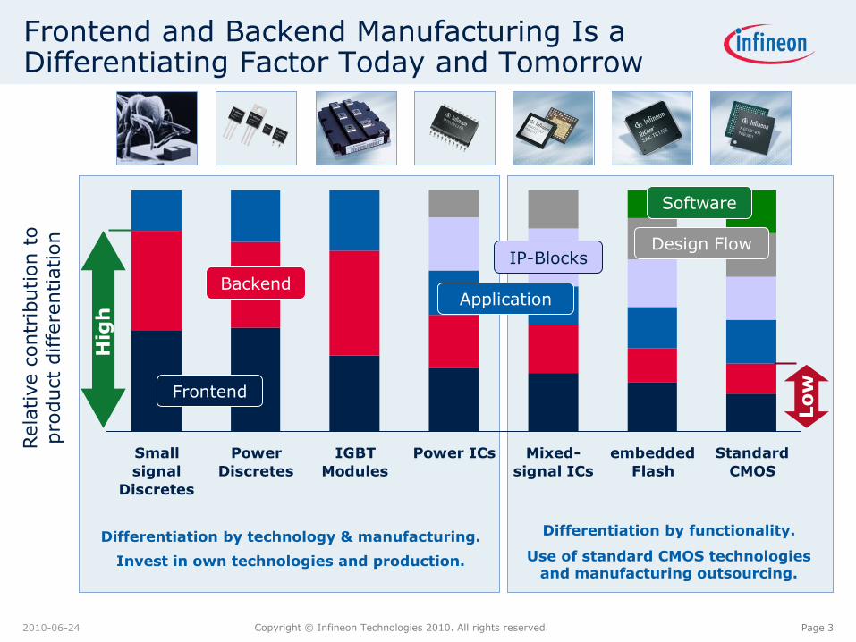
Frontend and Backend Manufacturing Is a Differentiating Factor Today and Tomorrow
Rela
tive c
ontr
ibution t
o
pro
duct
diffe
rentiation
Differentiation by functionality.
Use of standard CMOS technologiesand manufacturing outsourcing.
Differentiation by technology & manufacturing.
Invest in own technologies and production.
Hig
h
Lo
w
Backend
Frontend
Application
IP-BlocksDesign Flow
Software
Page 4Copyright © Infineon Technologies 2010. All rights reserved. 2010-06-24
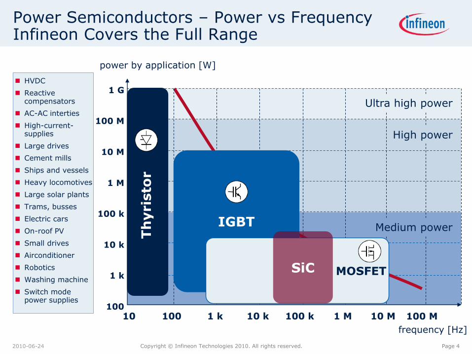
Power Semiconductors – Power vs Frequency Infineon Covers the Full Range
HVDC
Reactive compensators
AC-AC interties
High-current-supplies
Large drives
Cement mills
Ships and vessels
Heavy locomotives
Large solar plants
Trams, busses
Electric cars
On-roof PV
Small drives
Airconditioner
Robotics
Washing machine
Switch mode power supplies
100
1 k
10 k
10010 10 k1 k 100 k 1 M 10 M 100 M
power by application [W]
100 k
1 M
10 M
100 M
1 G
Ultra high power
High power
Medium powerIGBT
MOSFET
Th
yris
tor
SiC
frequency [Hz]

Page 5Copyright © Infineon Technologies 2010. All rights reserved. 2010-06-24
The Bridge Between Logic and Power: SPT9 (130nm) Puts Infineon into a Leading Positon
level of integration
100.1 100
switching current [A]
1
MOSFET
SoC,SiP
µC
control logic,state machine
statusprotection
single transistor
Smart
SPT1.0µm - 0.13µm
CMOS
HITFETPROFETTEMPFET
CoolMOSOptiMOS
SPT = Smart Power Technology
Page 6Copyright © Infineon Technologies 2010. All rights reserved. 2010-06-24
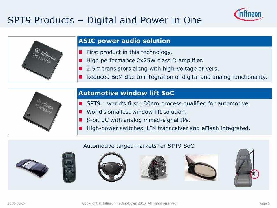
SPT9 Products – Digital and Power in One
Automotive window lift SoC
SPT9 world’s first 130nm process qualified for automotive.
World’s smallest window lift solution.
8-bit µC with analog mixed-signal IPs.
High-power switches, LIN transceiver and eFlash integrated.
ASIC power audio solution
First product in this technology.
High performance 2x25W class D amplifier.
2.5m transistors along with high-voltage drivers.
Reduced BoM due to integration of digital and analog functionality.
Automotive target markets for SPT9 SoC

Page 7Copyright © Infineon Technologies 2010. All rights reserved. 2010-06-24
Infineon's In-house Manufacturing Is Focusing on Embedded Flash, Sensor and Power
Regensburg
Kulim
Dresden
Villach
Employees: 1,090Capacity: 42k WSPMTechnology: >350nmComplexity: 16 mask layersProducts: Power
Employees: 990Capacity: 51k WSPMTechnology: >200nmComplexity: 13 mask layersProducts: Power, CMOS
Employees: 1,790Capacity: 40k WSPMTechnology: >90nmComplexity: 30 mask layersProducts: CMOS
Employees: 1,590Capacity: 110k WSPMTechnology: >200nmComplexity: 11 mask layersProducts: Power
ATV 20%
Lantiq 5%
WLS 10%
CCS 60%
IMM 5%ATV 65%Lantiq 5%
IMM 25%
WLS 5%
ATV 20%
IMM 70%
ATV 55%
IMM 45%
WSPM = Wafer Starts Per Month (200mm equivalent)
CCS 10%
Page 8Copyright © Infineon Technologies 2010. All rights reserved. 2010-06-24
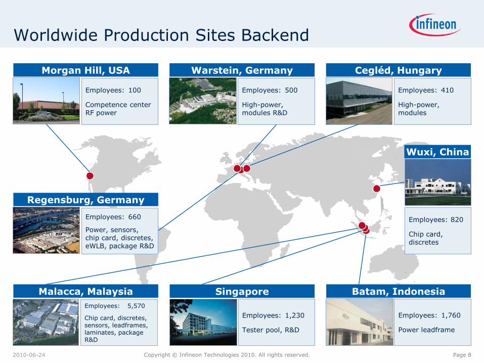
Worldwide Production Sites Backend
Regensburg, Germany
Employees: 660
Power, sensors, chip card, discretes, eWLB, package R&D
Morgan Hill, USA
Employees: 100
Competence center RF power
Warstein, Germany
Employees: 500
High-power, modules R&D
Cegléd, Hungary
Employees: 410
High-power, modules
Wuxi, China
Employees: 820
Chip card, discretes
Malacca, Malaysia
Employees: 5,570
Chip card, discretes, sensors, leadframes, laminates, package R&D
Batam, Indonesia
Employees: 1,760
Power leadframe
Singapore
Employees: 1,230
Tester pool, R&D
Page 9Copyright © Infineon Technologies 2010. All rights reserved. 2010-06-24
Table of Contents
Manufacturing Strategy
Competitive Advantage of In-house Frontend Manufacturing
Competitive Advantage of In-house Backend Manufacturing
Development of Outsourcing
Flexible Fab Management and Outlook
Page 10Copyright © Infineon Technologies 2010. All rights reserved. 2010-06-24
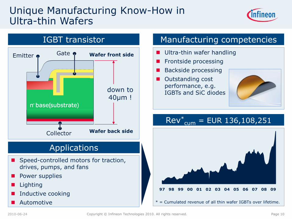
Unique Manufacturing Know-How inUltra-thin Wafers
down to40µm !
Wafer back side
Wafer front side
Applications
Speed-controlled motors for traction, drives, pumps, and fans
Power supplies
Lighting
Inductive cooking
Automotive
Manufacturing competencies
Ultra-thin wafer handling
Frontside processing
Backside processing
Outstanding costperformance, e.g.IGBTs and SiC diodes
IGBT transistor
Collector
Emitter Gate
n-base(substraten-base(substrate)
Rev*cum = EUR 136,108,251
* = Cumulated revenue of all thin wafer IGBTs over lifetime.
97 98 99 00 01 02 03 04 05 06 07 08 09
Page 11Copyright © Infineon Technologies 2010. All rights reserved. 2010-06-24
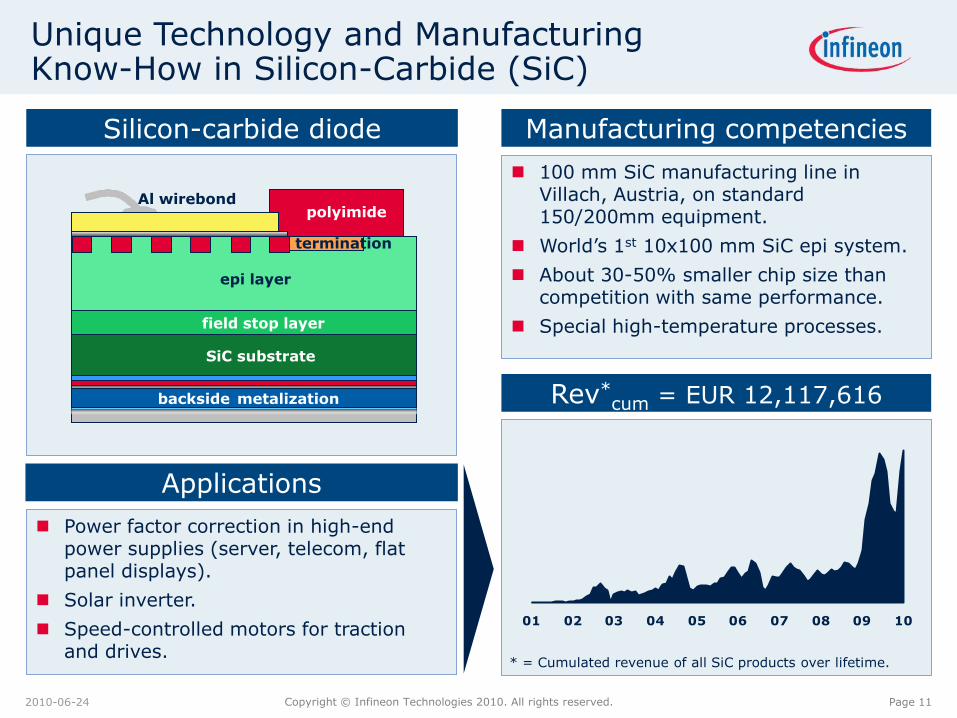
Unique Technology and Manufacturing Know-How in Silicon-Carbide (SiC)
Power factor correction in high-end power supplies (server, telecom, flat panel displays).
Solar inverter.
Speed-controlled motors for traction and drives.
100 mm SiC manufacturing line in Villach, Austria, on standard 150/200mm equipment.
World’s 1st 10x100 mm SiC epi system.
About 30-50% smaller chip size than competition with same performance.
Special high-temperature processes.
Applications
Manufacturing competenciesSilicon-carbide diode
Al wirebond
epi layer
SiC substrate
backsidemetalization
field stop layer
polyimide
termination
epi layer
SiC substrate
backside metalization
field stop layer
polyimide
termination
Rev*cum = EUR 12,117,616
* = Cumulated revenue of all SiC products over lifetime.
01 02 03 04 05 06 07 08 09 10

Page 12Copyright © Infineon Technologies 2010. All rights reserved. 2010-06-24
Outstanding Electrical Performance With CoolMOS™ Super-Junction Power MOSFETs
Power supplies for servers, PCs, notebooks, games consoles, adapters.
Graphics boards
Lighting
Solar inverter
Automotive
In the late 1990s, a super-junction transistor was invented, dubbed CoolMOS™.
Manufacturing improvements led to a cost reduction by a factor of 4.
Reduction of RDS(on) by a factor of 6.
Applications
Manufacturing competenciesSuper-junction transistor
Rev*cum = EUR 1,382,570,554
* = Cum. revenue of all CoolMOS™ products over lifetime.
97 98 99 00 01 02 03 04 05 06 07 08 09
Planar Super-junction
D
GS
D
GS
p p
Page 13Copyright © Infineon Technologies 2010. All rights reserved. 2010-06-24
Table of Contents
Manufacturing Strategy
Competitive Advantage of In-house Frontend Manufacturing
Competitive Advantage of In-house Backend Manufacturing
Development of Outsourcing
Flexible Fab Management and Outlook
Page 14Copyright © Infineon Technologies 2010. All rights reserved. 2010-06-24
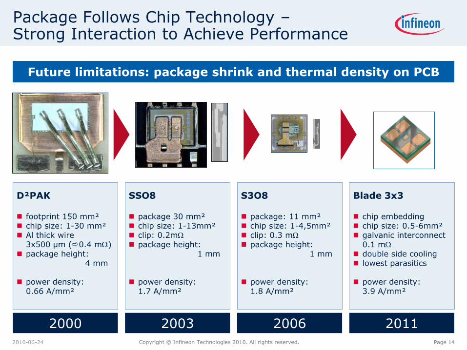
Package Follows Chip Technology –Strong Interaction to Achieve Performance
Future limitations: package shrink and thermal density on PCB
D²PAK
footprint 150 mm² chip size: 1-30 mm² Al thick wire
3x500 µm (0.4 m) package height:
4 mm
power density:0.66 A/mm²
SSO8
package 30 mm² chip size: 1-13mm² clip: 0.2m
package height:1 mm
power density:1.7 A/mm²
S3O8
package: 11 mm² chip size: 1-4,5mm² clip: 0.3 m
package height:1 mm
power density:1.8 A/mm²
Blade 3x3
chip embedding chip size: 0.5-6mm² galvanic interconnect
0.1 m
double side cooling lowest parasitics
power density: 3.9 A/mm²
2000 2003 2006 2011

Page 15Copyright © Infineon Technologies 2010. All rights reserved. 2010-06-24
Infineon Improved Power Density of Power Modules by More Than 180% Since 1995
State-of-the-art power modules and chips enable higher power density
IGBT2
34mm module
1200 V
45 kW
0.46 kW/cm2
Tj=125 C
IGBT3
EconoPACK™2
1200 V
37.2 kW
0.89 kW/cm2
Tj=125 C
IGBT4
EasyPACK2B
1200 V
31.3 kW
1.16 kW/cm2
Tj=150 C
IGBT4.XT
PrimePACK™2
1200 V
600 kW
1.31 kW/cm2
Tj=175 C
1995 2001 2007 2011
Page 16Copyright © Infineon Technologies 2010. All rights reserved. 2010-06-24
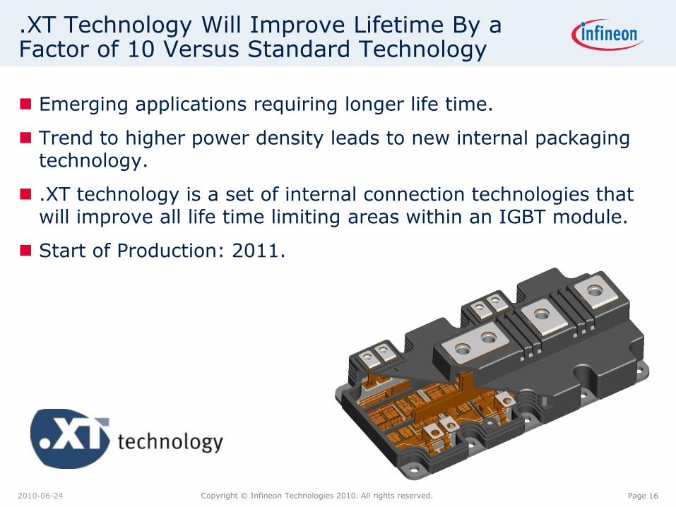
.XT Technology Will Improve Lifetime By a Factor of 10 Versus Standard Technology
Emerging applications requiring longer life time.
Trend to higher power density leads to new internal packaging technology.
.XT technology is a set of internal connection technologies that will improve all life time limiting areas within an IGBT module.
Start of Production: 2011.

Page 17Copyright © Infineon Technologies 2010. All rights reserved. 2010-06-24
What Is .XT Technology?
Si chip
DCB
Si chip
DCB
Si chip
DCB
base plate
Chip-to-substrate joint
Front side interconnect
Substrate-to-base plate joint
Soft soldering with SnAg paste
Diffusion soldering
Al wedge bonding Cu wedge bonding
Soft soldering with SnAg pre-form
High reliability system soldering
Standard technology
Page 18Copyright © Infineon Technologies 2010. All rights reserved. 2010-06-24
Table of Contents
Manufacturing Strategy
Competitive Advantage of In-house Frontend Manufacturing
Competitive Advantage of In-house Backend Manufacturing
Development of Outsourcing
Flexible Fab Management and Outlook

Page 19Copyright © Infineon Technologies 2010. All rights reserved. 2010-06-24
Differentiating Technologies In-house;Standard CMOS Technologies Outsourced
≥ 500nm 350 – 220nm 180nm 130 - 90nm 65nm ≤ 40nm
DresdeneFlash, special technologies (e.g. SPT 9)
KulimPower technologies
VillachPower technologies
RegensburgPower technologies
AltisFoundry partners
IBM
UMC
TSMC ( incl. eFlash)
GlobalFoundries
Bipolar JVHigh-power technologies
ASMC
In-house manufacturing
Innovation fabs
Best cost location
Competence center
RegensburgPower technologies
Bipolar JVHigh-power technologies
VillachPower technologies
RegensburgPower technologies
Bipolar JVHigh-power technologies
Power CMOS
Page 20Copyright © Infineon Technologies 2010. All rights reserved. 2010-06-24
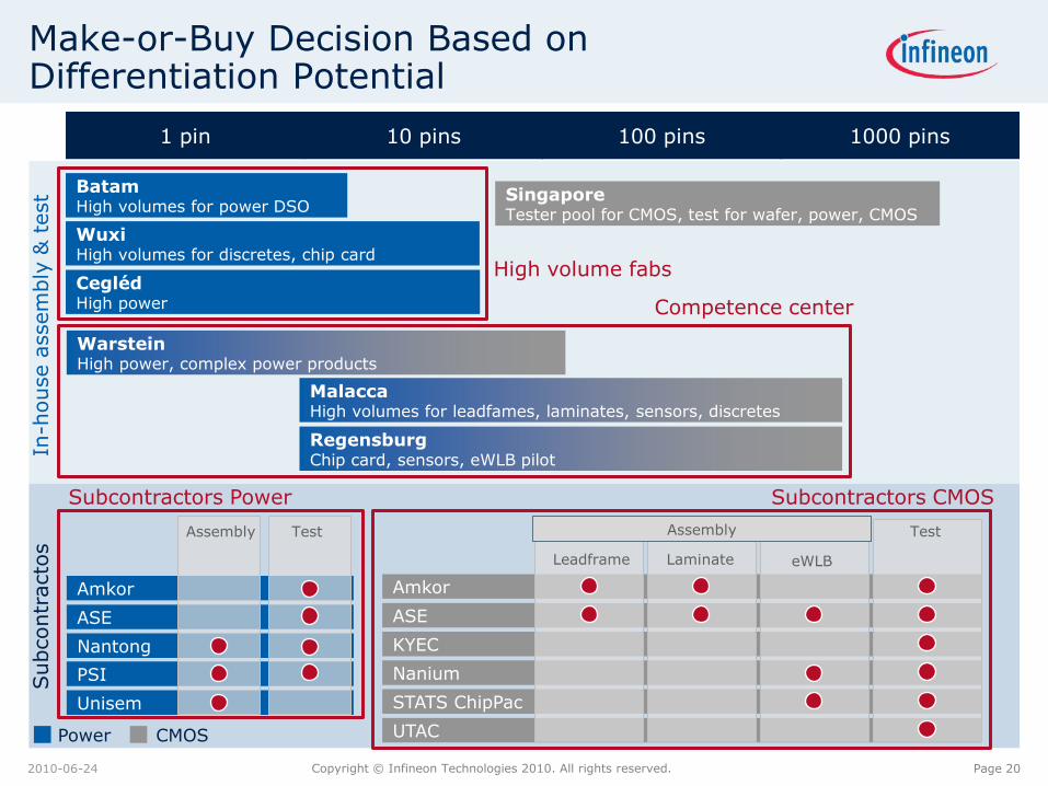
Make-or-Buy Decision Based on Differentiation Potential
1 pin 10 pins 100 pins 1000 pins
In-h
ouse a
ssem
bly
& t
est
Subcontr
acto
s
Subcontractors Power
CeglédHigh power
WarsteinHigh power, complex power products
BatamHigh volumes for power DSO
WuxiHigh volumes for discretes, chip card
High volume fabs
Competence center
SingaporeTester pool for CMOS, test for wafer, power, CMOS
MalaccaHigh volumes for leadfames, laminates, sensors, discretes
RegensburgChip card, sensors, eWLB pilot
Subcontractors CMOS
Amkor
ASE
KYEC
Nanium
STATS ChipPac
UTAC
Leadframe Laminate eWLB
Test
Amkor
ASE
PSI
Unisem
Nantong
Assembly Test Assembly
Power CMOS
Page 21Copyright © Infineon Technologies 2010. All rights reserved. 2010-06-24
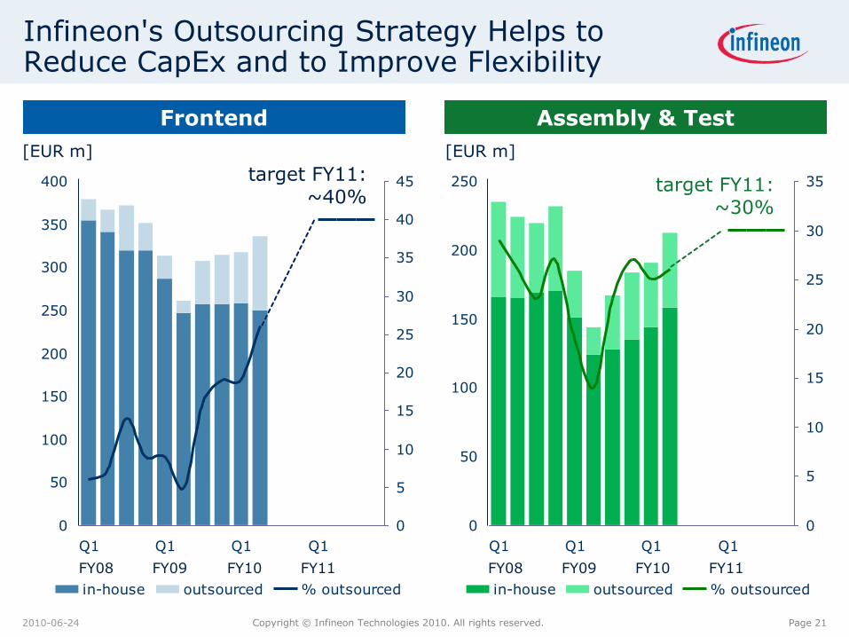
Frontend Assembly & Test
Infineon's Outsourcing Strategy Helps to Reduce CapEx and to Improve Flexibility
0
50
100
150
200
250
300
350
400
Q1 Q1 Q1 Q1
0
5
10
15
20
25
30
35
40
45
in-house outsourced % outsourced
[EUR m]
0
50
100
150
200
250
Q1 Q1 Q1 Q1
0
5
10
15
20
25
30
35
in-house outsourced % outsourced
[EUR m]
target FY11:~40%
target FY11:~30%
FY08 FY09 FY10 FY11 FY08 FY09 FY10 FY11
Page 22Copyright © Infineon Technologies 2010. All rights reserved. 2010-06-24
Table of Contents
Manufacturing Strategy
Competitive Advantage of In-house Frontend Manufacturing
Competitive Advantage of In-house Backend Manufacturing
Development of Outsourcing
Flexible Fab Management and Outlook
Page 23Copyright © Infineon Technologies 2010. All rights reserved. 2010-06-24
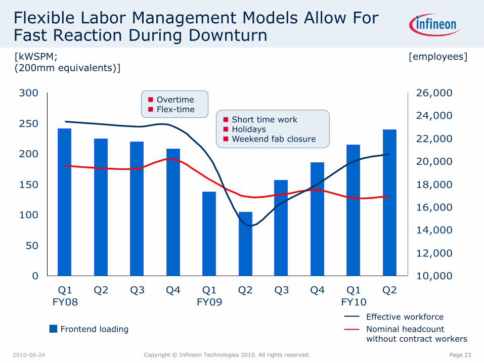
Flexible Labor Management Models Allow For Fast Reaction During Downturn
0
50
100
150
200
250
300
Q1
FY08
Q2 Q3 Q4 Q1
FY09
Q2 Q3 Q4 Q1
FY10
Q2
10,000
12,000
14,000
16,000
18,000
20,000
22,000
24,000
26,000
[kWSPM;(200mm equivalents)]
[employees]
Frontend loading Nominal headcountwithout contract workers
Effective workforce
Overtime Flex-time
Short time work Holidays Weekend fab closure
Page 24Copyright © Infineon Technologies 2010. All rights reserved. 2010-06-24
FY2008 FY2009 Q1 FY10 Q2 FY10 FY2010e Target
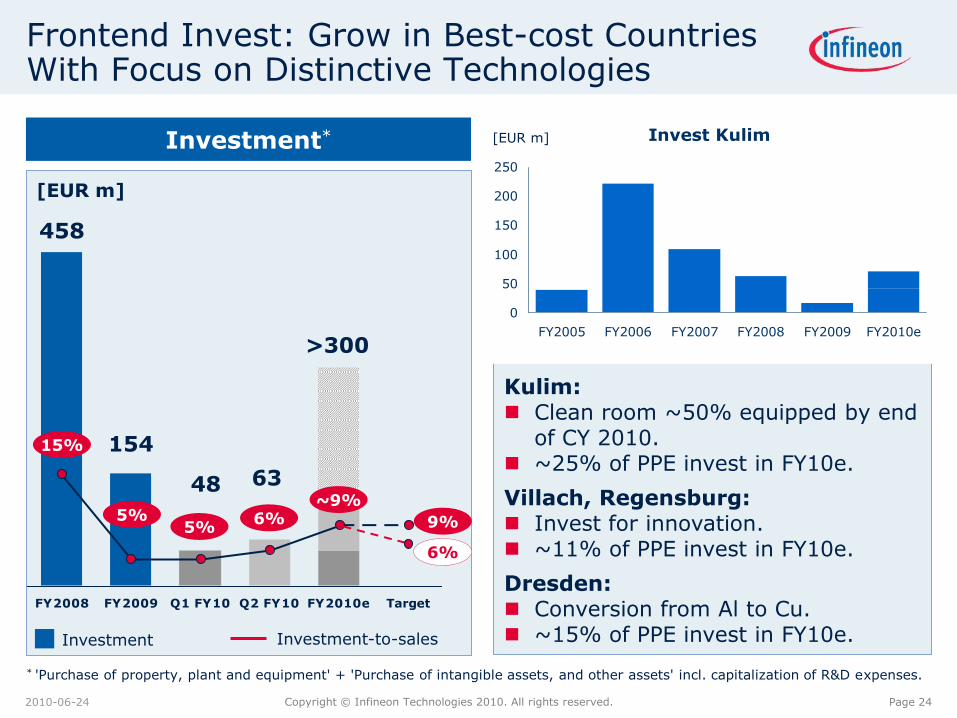
Frontend Invest: Grow in Best-cost CountriesWith Focus on Distinctive Technologies
* 'Purchase of property, plant and equipment' + 'Purchase of intangible assets, and other assets' incl. capitalization of R&D expenses.
Investment*
[EUR m]
154
48 63
>300
5%5%
6%~9%
9%
6%
Investment Investment-to-sales
15%
458
Kulim: Clean room ~50% equipped by end
of CY 2010. ~25% of PPE invest in FY10e.
Villach, Regensburg: Invest for innovation. ~11% of PPE invest in FY10e.
Dresden: Conversion from Al to Cu. ~15% of PPE invest in FY10e.
Invest Kulim
0
50
100
150
200
250
FY2005 FY2006 FY2007 FY2008 FY2009 FY2010e
[EUR m]


Page 26Copyright © Infineon Technologies 2010. All rights reserved. 2010-06-24
Disclaimer
This presentation was prepared as of June 24, 2010 and is current only as of that date.
This presentation includes forward-looking statements about the future of Infineon’s business and the industry in which we operate. These include statements relating to general economic conditions, future developments in the world semiconductor market, our ability to manage our costs and to achieve our growth targets, the resolution of Qimonda’s insolvency proceedings and the liabilities we may face as a result of Qimonda’s insolvency, the potential disposition or closure of our ALTIS joint venture, the benefits of research and development alliances and activities, our planned levels of future investment, the introduction of new technology at our facilities, our continuing ability to offer commercially viable products, and our expected or projected future results.
These forward-looking statements are subject to a number of uncertainties, such as broader economic developments, including the sustainability of recent improvements in the market environment; trends in demand and prices for semiconductors generally and for our products in particular, as well as for the end-products, such as automobiles and consumer electronics, that incorporate our products; the success of our development efforts, both alone and with partners; the success of our efforts to introduce new production processes at our facilities; the actions of competitors; the availability of funds; the outcome of antitrust investigations and litigation matters; and the resolution of Qimonda’s insolvency proceedings; as well as the other factors mentioned in this presentation and those described in the “Risk Factors” section of our most recent annual report on Form 20-F on file with the U.S. Securities and Exchange Commission. As a result, Infineon’s actual results could differ materially from those contained in or suggested by these forward-looking statements. You are cautioned not to place undue reliance on these forward-looking statements.
Infineon does not undertake any obligation to publicly update or revise any forward-looking statements in light of developments which differ from those anticipated.