Embed Size (px)
Citation preview

IEEE TRANSACTIONS ON VERY LARGE SCALE INTEGRATION (VLSI) SYSTEMS, VOL. 18, NO. 4, APRIL 2010 517
Computation Error Analysis in Digital SignalProcessing Systems With Overscaled Supply Voltage
Yang Liu, Student Member, IEEE, Tong Zhang, Senior Member, IEEE, and Keshab K. Parhi, Fellow, IEEE
Abstract—It has been recently demonstrated that digitalsignal processing systems may possibly leverage unconventionalvoltage overscaling (VOS) to reduce energy consumption whilemaintaining satisfactory signal processing performance. Dueto the computation-intensive nature of most signal processingalgorithms, the energy saving potential largely depends on thebehavior of computer arithmetic units in response to overscaledsupply voltage. This paper shows that different hardware imple-mentations of the same computer arithmetic function may respondto VOS very differently and result in different energy saving poten-tials. Therefore, the selection of appropriate computer arithmeticarchitecture is an important issue in voltage-overscaled signal pro-cessing system design. This paper presents an analytical method toestimate the statistics of computer arithmetic computation errorsdue to supply voltage overscaling. Compared with computation-in-tensive circuit simulations, this analytical approach can be severalorders of magnitude faster and can achieve a reasonable accuracy.This approach can be used to choose the appropriate computerarithmetic architecture in voltage-overscaled signal processingsystems. Finally, we carry out case studies on a coordinate rotationdigital computer processor and a finite-impulse-response filter tofurther demonstrate the importance of choosing proper computerarithmetic implementations.
Index Terms—Computation error analysis, computer arith-metic, digital signal processing, voltage overscaling (VOS).
I. INTRODUCTION
V OLTAGE SCALING is an effective technique to reducethe energy consumption in CMOS integrated circuits [1],
[2]. In conventional practice, voltage scaling is lower boundedby , under which the critical path delay equals the targetclock period. Voltage overscaling (VOS), i.e., overscaling thesupply voltage below , can result in transient circuittiming errors, which is generally not allowed in current designpractice. It is well known that there is a large degree of discrep-ancy between the average-case and the worst-case circuit delayin practice, particularly in many computer arithmetic functions.This suggests that, even under an overscaled supply voltage,computer arithmetic functions may have a relatively low prob-ability to produce errors in each clock cycle. Intuitively, thisfeature may be exploited to enable the use of VOS to reducethe energy consumption of computational datapath, as demon-strated in recent works [3]–[6]. In this context, the key issue is
Manuscript received June 17, 2008; revised October 19, 2008 and January 04,2009. First published June 16, 2009; current version published March 24, 2010.
Y. Liu and T. Zhang are with the Department of Electrical, Computer, andSystems Engineering, Rensselaer Polytechnic Institute, Troy, NY 12180 USA(e-mail: [email protected]; [email protected]).
K. K. Parhi is with the Department of Electrical and Computer Engineering,University of Minnesota, Minneapolis, MN 55455 USA (e-mail: [email protected]).
Digital Object Identifier 10.1109/TVLSI.2009.2012863
how to maintain the satisfactory functionality in the presenceof the transient errors incurred by VOS while ensuring that theoverall system energy consumption is reduced. The techniquesproposed in [3] and [4] tackle this issue by using a detect/spec-ulate-then-recover mechanism, i.e., first, the occurrence of tran-sient errors is either speculated [3] based on run-time data char-acteristics or detected [4] using special circuitry, and then, cer-tain system-level operations are executed to recover the errors.This type of approach is suitable to applications such as gen-eral-purpose computing that may tolerate the latency overheaddue to error recovery operations. However, they may not be ap-plicable to most digital signal processing functions that typicallyperform real-time continuous data processing, which makes itdifficult to support such a detect/speculate-then-recover flow.
Particularly targeting digital signal processing systems, thedesign methodology proposed in [5] and [6] intends to compen-sate the signal processing performance degradation incurred bytransient errors instead of trying to recover all the errors. It canbe justified by the fact that, as pointed out in [5] and [6], mostsignal processing functions mainly address certain quantitativehigh-level performance criteria [e.g., signal-to noise ratio(SNR)] and that circuit transient errors may not necessarilymake the signal processing performance unacceptable. Tech-niques for compensating the signal processing performancedegradation incurred by VOS have been developed for linearfilters [5], [7], [8] and fast Fourier transform [9]. Furthermore,it is not uncommon that signal processing systems are designedto meet a stringent system performance criterion in order tohandle the worst-case run-time scenario, which may be far morestringent for average cases. Intuitively, this provides a potentialto directly apply VOS for energy reduction without using anyperformance compensation schemes in some circumstances.
In most signal processing systems, various computer arith-metic functions, particularly addition and multiplication, aremajor building blocks and typically constitute the critical paths.Therefore, the signal processing performance degradationincurred by VOS heavily depends on the output transient errorcharacteristics of those computer arithmetic functions in re-sponse to overscaled supply voltage. All the prior works [5]–[9]on voltage-overscaled signal processing system design assumedthe use of carry-ripple adder architecture in the realizations ofadders and multipliers. Intuitively, different computer arith-metic architectures (e.g., carry-ripple adder, carry-select adder,and carry-lookahead adder) may respond to overscaled supplyvoltage differently, leading to different output transient errorcharacteristics, even though they have the same critical pathdelay. This will further result in different signal processingperformance degradation and, hence, different energy savingpotentials in voltage-overscaled signal processing systems.
1063-8210/$26.00 © 2010 IEEE
518 IEEE TRANSACTIONS ON VERY LARGE SCALE INTEGRATION (VLSI) SYSTEMS, VOL. 18, NO. 4, APRIL 2010
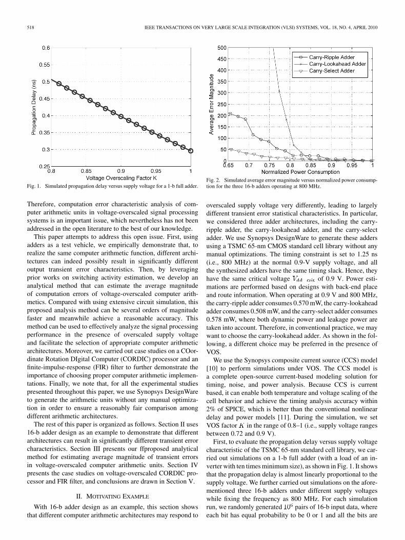
Fig. 1. Simulated propagation delay versus supply voltage for a 1-b full adder.
Therefore, computation error characteristic analysis of com-puter arithmetic units in voltage-overscaled signal processingsystems is an important issue, which nevertheless has not beenaddressed in the open literature to the best of our knowledge.
This paper attempts to address this open issue. First, usingadders as a test vehicle, we empirically demonstrate that, torealize the same computer arithmetic function, different archi-tectures can indeed possibly result in significantly differentoutput transient error characteristics. Then, by leveragingprior works on switching activity estimation, we develop ananalytical method that can estimate the average magnitudeof computation errors of voltage-overscaled computer arith-metics. Compared with using extensive circuit simulation, thisproposed analysis method can be several orders of magnitudefaster and meanwhile achieve a reasonable accuracy. Thismethod can be used to effectively analyze the signal processingperformance in the presence of overscaled supply voltageand facilitate the selection of appropriate computer arithmeticarchitectures. Moreover, we carried out case studies on a COor-dinate Rotation DIgital Computer (CORDIC) processor and anfinite-impulse-response (FIR) filter to further demonstrate theimportance of choosing proper computer arithmetic implemen-tations. Finally, we note that, for all the experimental studiespresented throughout this paper, we use Synopsys DesignWareto generate the arithmetic units without any manual optimiza-tion in order to ensure a reasonably fair comparison amongdifferent arithmetic architectures.
The rest of this paper is organized as follows. Section II uses16-b adder design as an example to demonstrate that differentarchitectures can result in significantly different transient errorcharacteristics. Section III presents our ffproposed analyticalmethod for estimating average magnitude of transient errorsin voltage-overscaled computer arithmetic units. Section IVpresents the case studies on voltage-overscaled CORDIC pro-cessor and FIR filter, and conclusions are drawn in Section V.
II. MOTIVATING EXAMPLE
With 16-b adder design as an example, this section showsthat different computer arithmetic architectures may respond to
Fig. 2. Simulated average error magnitude versus normalized power consump-tion for the three 16-b adders operating at 800 MHz.
overscaled supply voltage very differently, leading to largelydifferent transient error statistical characteristics. In particular,we considered three adder architectures, including the carry-ripple adder, the carry-lookahead adder, and the carry-selectadder. We use Synopsys DesignWare to generate these addersusing a TSMC 65-nm CMOS standard cell library without anymanual optimizations. The timing constraint is set to 1.25 ns(i.e., 800 MHz) at the normal 0.9-V supply voltage, and allthe synthesized adders have the same timing slack. Hence, theyhave the same critical voltage of 0.9 V. Power esti-mations are performed based on designs with back-end placeand route information. When operating at 0.9 V and 800 MHz,the carry-ripple adder consumes 0.570 mW, the carry-lookaheadadder consumes 0.508 mW, and the carry-select adder consumes0.578 mW, where both dynamic power and leakage power aretaken into account. Therefore, in conventional practice, we maywant to choose the carry-lookahead adder. As shown in the fol-lowing, a different choice may be preferred in the presence ofVOS.
We use the Synopsys composite current source (CCS) model[10] to perform simulations under VOS. The CCS model isa complete open-source current-based modeling solution fortiming, noise, and power analysis. Because CCS is currentbased, it can enable both temperature and voltage scaling of thecell behavior and achieve the timing analysis accuracy within2% of SPICE, which is better than the conventional nonlineardelay and power models [11]. During the simulation, we setVOS factor in the range of 0.8–1 (i.e., supply voltage rangesbetween 0.72 and 0.9 V).
First, to evaluate the propagation delay versus supply voltagecharacteristic of the TSMC 65-nm standard cell library, we car-ried out simulations on a 1-b full adder (with a load of an in-verter with ten times minimum size), as shown in Fig. 1. It showsthat the propagation delay is almost linearly proportional to thesupply voltage. We further carried out simulations on the afore-mentioned three 16-b adders under different supply voltageswhile fixing the frequency as 800 MHz. For each simulationrun, we randomly generated pairs of 16-b input data, whereeach bit has equal probability to be 0 or 1 and all the bits are

LIU et al.: COMPUTATION ERROR ANALYSIS IN SYSTEMS WITH OVERSCALED SUPPLY VOLTAGE 519
Fig. 3. Simulated bit error rate versus normalized power consumption for thethree 16-b adders operating at 800 MHz.
randomly generated independent from each other. Fig. 2 showsthe simulated average error magnitude versus normalized powerconsumption, where the average error magnitude is the mean ofthe computation error magnitude over all the simulated samplesand the power consumptions are normalized against the highestpower consumption among all the adders under a normal supplyvoltage. Fig. 3 shows the simulated average bit error rate (i.e.,the number of bits that is wrongly computed) versus normalizedpower consumption. It shows that, under an overscaled supplyvoltage, the carry-ripple adder has the least bit error rate, whilethe carry-select adder has the least performance degradation ifwe take into account the significance of each output bit. Al-though all the adders have similar bit error rates (i.e., 0.06–0.14),they have very different average error magnitudes, as shown inFig. 2. Since the performance degradation of signal processingsystems under an overscaled voltage heavily depends on thecomputation error magnitude, the aforesaid results suggest thatwe should not use mere computation bit error rate as a metric toselect the appropriate arithmetic architecture and that we shouldbe able to directly estimate the average error magnitude charac-teristics for each candidate arithmetic architecture.
Fig. 4 further shows the relations between the error occur-rence probability for each bit and the supply voltage for thesethree adders. Bits 0, 15, and 16 correspond to the least signifi-cant bit (LSB), most significant bit (MSB), and adder carry out,respectively. It is clear that Fig. 4 can approximately explain thedifferent average error magnitude versus supply voltage charac-teristics among the three adders, as shown in Fig. 2. The dif-ferent error distribution characteristics, as shown in Fig. 4, maybe intuitively explained as follows.
1) In a carry-ripple adder, a more significant bit has longerworst-case delay and can hence be more subject to errors.On the other hand, the worst-case-delay paths of a moresignificant bit tend to be activated less frequently. Due tothese two somehow conflicting trends, the error occurrenceprobabilities of those more significant bits tend to be flat,as shown in Fig. 4(a).
Fig. 4. Error occurrence probability of each bit of the three different adders.(a) Error distributions of the carry-ripple adder. (b) Error distributions of thecarry-lookahead adder. (c) Error distributions of the carry-select adder.
2) A carry-lookahead adder consists of several segments thatform a carry-lookahead chain, and within each segment, acarry-ripple adder should be used. As a result, the MSBswithin each segment tend to have similar worst-case delaythat are the same or close to the overall carry-lookahead-adder critical path. Therefore, these MSBs within all thesegments are more subject to errors, as shown in Fig. 4(b).

520 IEEE TRANSACTIONS ON VERY LARGE SCALE INTEGRATION (VLSI) SYSTEMS, VOL. 18, NO. 4, APRIL 2010
3) A carry-select adder also consists of several segments.However, the two possible addition results of each segment(corresponding to the two scenarios in which the carryinput to this segment is 0 and 1) are precomputed and aresimply selected by the carry input. Therefore, the less sig-nificant bits within each segment may be more subject toerrors compared with the more significant bits in the samesegment. Since the adder is generated using DesignWare,the segment partition information is not readily available.From Fig. 4(c), we guess that the bits around bit positions8 and 12 are LSBs within two adjacent segments.
The aforementioned results suggest that, even though thecarry-lookahead adder has the minimum power consumptionunder a normal supply voltage, the carry-select adder may bepreferred in voltage-overscaled digital signal processing systemdesign since the average error magnitude may directly affectthe signal processing performance degradation.
III. ERROR ANALYSIS OF VOLTAGE-OVERSCALED COMPUTER
ARITHMETICS
Since different computer arithmetic implementations may re-spond to overscaled supply voltage very differently, it is highlydesirable to develop a method that can quantitatively reveal thetransient error characteristics of various computer arithmeticimplementations. Although brute-force circuit simulations canserve this purpose, it suffers from very high computational com-plexity, even for small circuits (e.g., a 16-b adder). This makes itimpossible to explore computer arithmetic design space over awide range of VOS by relying on circuit simulations and hencedemands analytical techniques that can efficiently estimate thetransient computation error characteristics while maintaining areasonable accuracy.
Motivated by the obvious correlation between the circuitswitching activity and transient computation error, this paperaims to develop computation error analysis techniques byleveraging prior works on circuit switching activity estimation.Generally speaking, the objective of switching activity esti-mation is to estimate the switching probabilities of each gatein circuits over time, given the switching probabilities of theinput. A variety of switching estimation techniques have beendeveloped with different accuracy versus efficiency tradeoffs,e.g., see [12]–[15].
A first glance may suggest that the estimated switching activ-ities of the computation output bits can be directly used to derivethe transient computation error characteristics in a very straight-forward manner, which unfortunately turns out to be wrong. Forexample, let us consider an 8-b unsigned carry-select adder, asshown in Fig. 5, where the critical path lies in the carry-selectsignal propagation. Suppose that the correct output should be10000000 at one time, but the output becomes 01110000 be-cause of a critical path violation due to VOS. Clearly, the outputerror magnitude is (i.e.,
). However, if we consider the switching of the outputbits independently, the magnitude of computation error becomes
since all the four MSBs switch to erro-neous values. This example shows that we cannot only rely onthe switching activity estimation of computation output bits to
Fig. 5. Structure of an 8-b carry-select adder.
derive the computation output error characteristics because ofthe correlation among the output-bit switching errors.
Therefore, we must explicitly preserve the correlationsamong the computation-output-bit switching errors. It is clearthat such correlations are due to the fact that each internalsignal (or the output of each logic gate) in computer arithmeticcircuits may contribute to more than one computation outputbit. For example, the carry-select signal in the previous ex-ample directly affects all the four most significant output bits.Therefore, the correlations among the computation-output-bitswitching errors can be revealed by explicitly observing thecontribution of each internal signal’s switching to the overallcomputation output error, which is referred to as the error sig-nificance of each internal signal. For any internal signal, letdenote the maximum computation error magnitude incurred bythe switching of this signal. Then, the error significance of thissignal depends on both its and switching activity. We call
as the error significance factor of this internal signal. In thefollowing, we first discuss how to derive the error significancefactor for each internal signal in computer arithmetic circuitsand then present how we may estimate the overall computationoutput error magnitude by combining the error significancefactors and switching activities.
A. Error Significance Factor Assignment
The error significance factor associated with each internalsignal in computer arithmetic circuits represents the maximumcomputation output error magnitude that is incurred if thepresent internal signal cannot propagate to the output bitsin time. For example, let us again consider the 8-b unsignedcarry-select adder, as shown in Fig. 5. As discussed previously,if a switch on the carry-select signal cannot propagate to thefour MSBs in time, the output error magnitude is .Hence, we have that the error significance factor of the carry-se-lect signal is eight. Motivated by this example, we have thefollowing simple rules to determine the error significance factorof each internal signal:
1) If an internal signal only contributes to one computationoutput bit, then its error significance factor is assignedas the weight of the corresponding output bit.
2) If an internal signal contributes to a group of computationoutput bits, then its error significance factor is assignedas the minimum one among the weights of the output-bitgroup.

LIU et al.: COMPUTATION ERROR ANALYSIS IN SYSTEMS WITH OVERSCALED SUPPLY VOLTAGE 521
Fig. 6. Pseudocode for the error significance factor assignment.
Fig. 7. Example of weight assignment.
In general, the th computation output bit has a weight of ,where corresponds to the LSB. Given the computer arith-metic circuit topology, we can use a simple trace-back procedureto automatically derive the error significance factor of each in-ternal signal, where the pseudocode is shown in Fig. 6. The in-puts of each gate are called parent signals of its output. Startingfrom the computation output bit with the highest weight (i.e.,the MSB), the weight of each output bit simply propagates back-ward through all the connected gates, and the later propagatedvalues overwrite the early ones. This is further shown in Fig. 7for a 3-b adder.
B. Computation Error Magnitude Estimation
Once the error significance factors of all the internal signals incomputer arithmetic circuits are determined, they will be com-bined with the internal signal switching activity information toestimate the average computation output error magnitude. De-note the probability that a signal is logic 1 at a particular timepoint as and the probability thatthe signal is logic 0 as . Each signal has fourpossible transitions (i.e., 0 0, 0 1, 1 1, and 1 0) betweentwo adjacent time points, and we denote the corresponding tran-sition probabilities as , , , and .The objective of switching activity estimation is to accuratelyestimate , , , and for all the gatesin the circuits at all the discrete time points. The granularity ofthe discrete-time-point sequence (i.e., the distance between twoadjacent time points) depends on the requirement of estimationaccuracy and the technology library being used. Readers are re-ferred to [12]–[15] for existing work on switching activity esti-mation. In this paper, we mainly use the approach addressed in[12] and [14] to calculate these transition probabilities.
Under an overscaled supply voltage, the critical path delay ofcomputer arithmetic circuits will be longer than the target clock
Fig. 8. Flowchart of computation output error estimation.
period (denoted as ). Hence, any switching inside the cir-cuits at time may potentially result in computation error,i.e., the average magnitude of the computation output errors in-curred by the switching of internal signal at can be esti-mated as
(1)
where is the error significance factor of internal signal .Assuming that all the switchings of the internal signals atwill independently and additively contribute to the computa-tion output error, we can estimate the average computation errormagnitude as
(2)
where the set contains all the internal signals in computerarithmetic circuits.
We further implemented a software package to realize theaforementioned computation output error estimation approach,where Fig. 8 shows the software flowchart. It extracts the cir-cuit topology from a synthesized gate-level netlist that is furthersorted by topological ordering [16] to facilitate the trace-backerror significance factor assignment procedure presented ear-lier. The timing information of the circuits is obtained from theback-annotated stand-delay-format files generated by the Syn-opsys CCS model under VOS.
For the purpose of evaluation, we apply this proposed ap-proach to the same three 16-b adders discussed in Section II(i.e., the carry-ripple adder, the carry-lookahead adder, and thecarry-select adder). Fig. 9 shows the analysis results and thecomparison with the results obtained from very time-consuminggate-level circuit simulations over 200 000 random input pairs.Furthermore, we also use Synopsys DesignWare to generatethree 16-input two’s-complement multipliers that use a carry-ripple adder, a carry-lookahead adder, or a carry-select adder asthe final-stage merge adder, respectively. They are denoted as

522 IEEE TRANSACTIONS ON VERY LARGE SCALE INTEGRATION (VLSI) SYSTEMS, VOL. 18, NO. 4, APRIL 2010
Fig. 9. Estimated and simulated average error magnitudes versus normalizedpower consumption for the three 16-b adders operating at 800 MHz.
CR-Multiplier, CL-Multiplier, and CS-Multiplier, respectively.All the three multipliers have the same timing slack and canrun at 500 MHz under the normal supply voltage of 0.9 V.Fig. 10 shows the analysis results for these three multipliersand the comparison with the results obtained from gate-levelcircuit simulations over 200 000 random input pairs. We notethat, in both Fig. 9 and Fig. 10, the absolute values of the es-timated and simulated results are somehow different, which isat least partially due to the estimation inaccuracy induced byignoring those deep correlations, as discussed earlier, but theyreveal the same comparative trends. Since our objective is todetermine which architecture should be selected, it is the com-parative trends, other than the absolute values, that is the mostimportant in this context. Fig. 11 shows the corresponding biterror rate for these three multipliers under an overscaled voltage.They clearly have different trends compared with the results onaverage error magnitude, as shown in Fig. 10.
In general, for -input -bit computation arithmetic circuits,the computational complexity of exhaustive gate-level simula-tions is on the order of , while the computational com-plexity of this analysis approach is the same as that of switchingactivity estimation techniques, which is usually on the orderof . This suggests orders of magnitude speedupby using the proposed analysis-based approach to estimate thecomputation error magnitude. For example, for the 16-b addersconsidered earlier, an exhaustive gate-level simulation may takeabout 16 h, while the proposed method only takes less than 1min.
IV. APPLICATIONS TO DIGITAL SIGNAL PROCESSING SYSTEM
DESIGN
This section presents case studies on voltage-overscaledCORDIC processor and FIR filter to further illustrate theimpact of various arithmetic unit architectures.
A. Case Study on CORDIC Processor
CORDIC processor is widely used in signal processing sys-tems to calculate hyperbolic, trigonometric, or logarithmic func-
Fig. 10. Estimated and simulated average error magnitudes versus normalizedpower consumption for the three 16-b multipliers operating at 500 MHz.
Fig. 11. Bit error rate versus normalized power consumption for the three 16-bmultipliers operating at 500 MHz.
tions without the implementation of multipliers [17]. This workconsiders using CORDIC processors to realize vector rotation[18], i.e., obtain the vector by rotating a vectorwith angle . CORDIC processors realize the vector rotation inan iterative manner, where the operations during each iterationare
where if ( 1 otherwise) and is the rotationangle in the binary representation. Fig. 12 shows the structureof an -stage pipelined CORDIC processor. In this case study,we set and employ 10-b two’s-complement fractionalnumber representation for the data.

LIU et al.: COMPUTATION ERROR ANALYSIS IN SYSTEMS WITH OVERSCALED SUPPLY VOLTAGE 523
Fig. 12. CORDIC structure.
Fig. 13. Estimated CORDIC processor performance under VOS based on theerror estimation of each adder.
We studied the impact of different adder architectures on theoperation of CORDIC processor under VOS. Using SynopsysDesignWare with the TSMC 65-nm CMOS standard cell library,we obtained four different flip-flop pipelined implementationsof the CORDIC processor where addition and subtraction
Fig. 14. Simulated CORDIC processor performance under VOS based on theMonte Carlo simulation of the entire CORDIC processor.
Fig. 15. FIR filter frequency response and run-time environment setup.
are realized by a carry-ripple adder, a carry-lookahead adder,a carry-select adder, and a Brent–Kung (BK) adder, respec-tively. We denote these four different CORDIC processors asCR-CORDIC, CL-CORDIC, CS-CORDIC, and BK-CORDIC,respectively. All these CORDIC processors have the samecritical path of 1.4 ns. The approach developed in Section III isused to evaluate the performance of CORDIC processors underoverscaled voltages. We assume that all the primary input bitsare statistically independent and have equal probability of being1 and 0. We first estimate the magnitude of computation errorsat each pipeline stage. Similar to conventional quantizationerror analysis [19], we treat these computation errors at eachstage as independent additive error sources, based on which weobtain the overall computation output average error magnitudethrough Monte Carlo simulations with 10 000 random samples.We assume that the performance of CORDIC processor ismeasured by
(3)
where is the signal power of error-free rotatedvector that is calculated by Matlab’s built-in trigono-metric function, is the variance of errors due to quantization

524 IEEE TRANSACTIONS ON VERY LARGE SCALE INTEGRATION (VLSI) SYSTEMS, VOL. 18, NO. 4, APRIL 2010
Fig. 16. Architecture of MAC �� � � � �� with sign–magnitude data input/output.
and limited number of iterations, and denotes the variance ofcomputation output errors due to overscaled voltage.
Fig. 13 shows the estimated SNR versus normalized powerconsumption under different overscaled voltages. Although thefour different CORDIC processors have the same critical path,they clearly respond to VOS very differently, and the estimationresults suggest that carry-lookahead and BK adders should beselected to achieve better power-performance tradeoff. More-over, as shown in Fig. 13, even if SNR performance is not al-lowed to be sacrificed, we may still use VOS to reduce thepower consumption by about 25% when either BK-CORDICor CL-CORDIC is used. To further testify this conclusion, weconducted much more time-consuming simulations on the entireCORDIC processor using these four different arithmetic units,and Fig. 14 shows the simulated SNR versus normalized powerconsumption, which agrees with the aforementioned conclusionthat BK-CORDIC or CL-CORDIC may be preferred. Althoughthe absolute values of estimations (as shown in Fig. 13) and sim-ulations (as shown in Fig. 14) are different, both estimations andsimulations reveal the same trends and comparisons among var-ious design options. Hence, the proposed estimation approachcan well serve the purpose of selecting appropriate computerarithmetic architecture.
B. Case Study on FIR Filter
The second case study is carried out on a 19-tap low-pass FIRfilter with passband, as shown in Fig. 15. ThisFIR filter intends to extract the desired signal within
from the interfering signals withinand additive white Gaussian noise (AWGN). Its filtering perfor-mance is measured in terms of SNR. For the finite word-lengthconfiguration, we use 17-b fixed-point representation for thefilter input/output, filter coefficients, and all the intermediatedata, where the point sits between the MSB and the secondMSB.
This FIR filter has a transposed structure, so it only containsone type of arithmetic unit, i.e., MAC at each filter tap. For thedesign of MAC, as pointed out in prior works [1], [5], usingsign–magnitude input data representation may reduce the dy-namic power consumption and, more importantly, reduce theerror occurrence on more significant bits of the MAC outputwhen VOS is being used. Therefore, we use the sign–magni-tude data representation for the input/output of the MACs, asshown in Fig. 16. Let and represent the mag-nitude and sign of the data, respectively. As shown in Fig. 16,
Fig. 17. Structure of the FIR filter.
the carry-save adder, followed by the merge adder, calculatesif equals ,
or otherwise, and the calcula-tion is realized by internally representingand with two’s-complement format. The output ofthe merge adder is intwo’s-complement representation. To obtain the magnitude of
, we further XOR its MSB with all the other bits and mean-while add its MSB to the LSB position. To remove the overheadincurred by such an extra addition in each MAC, we can delayit to the final FIR filter output and refer the MSB of as theresidual LSB output, as shown in Fig. 16. Accordingly, we havethe overall FIR filter structure, as shown in Fig. 17.
Again, the TSMC 65-nm standard cell library is used tosynthesize the FIR filter. We implemented four different MACsthat only differ at the merge adder, where a carry-ripple adder,a carry-lookahead adder, a carry-select adder, or a BK adderis used. We denote these four different MACs as CR-MAC,CL-MAC, CS-MAC, and BK-MAC, respectively. The fourMACs have the same critical path of 3.6 ns. We use the same(3) in the previous to calculate the SNR of the FIR filter, exceptthat now denotes the variance of AWGN. The power ofAWGN is 38 dB, corresponding to . Sincethe filtering performance is measured in terms of SNR, thevariance of the MAC output error is used in the calculation.Fig. 18 shows the estimated SNR versus normalized powerconsumption. It suggests that CL-MAC and BK-MAC canachieve modestly better power-performance tradeoff.
We further carried out extensive simulations on the entireFIR filter to evaluate the effects when different MACs are usedunder VOS. Fig. 19 shows the simulated SNR versus normalizedpower consumption, which agrees with the previous conclusionthat CL-MAC or CR-MAC may be preferred. Again, althoughthe absolute values of estimations and simulations are different,

LIU et al.: COMPUTATION ERROR ANALYSIS IN SYSTEMS WITH OVERSCALED SUPPLY VOLTAGE 525
Fig. 18. Estimated FIR performance under VOS based on the error estimationof each MAC.
Fig. 19. Simulated FIR performance under VOS based on the Monte Carlosimulation of the entire FIR filter.
they reveal the same trends and comparisons among various de-sign options.
V. CONCLUSION
This paper addressed the issue of computation error analysisof computer arithmetic units in voltage-overscaled signal pro-cessing systems. For the first time, we showed that differentarithmetic unit architectures may respond to VOS very differ-ently, which would result in different energy saving potentials.For the search of proper computer arithmetic architecture,we developed an analytical method that could efficiently es-timate the computation error statistics of computer arithmeticunits under an overscaled voltage. Moreover, for the purpose ofdemonstration, we presented case studies on voltage-overscaledCORDIC processor and FIR filter. In the future, we will take
efforts on extending our work to support more kinds of errorsand taking technology process variations into account.
REFERENCES
[1] A. P. Chandrakasan and R. W. Brodersen, “Minimizing power con-sumption in digital CMOS circuits,” Proc. IEEE, vol. 83, no. 4, pp.498–523, Apr. 1995.
[2] R. Gonzalez, B. M. Gordon, and M. A. Horowitz, “Supply andthreshold voltage scaling for low power CMOS,” IEEE J. Solid-StateCircuits, vol. 32, no. 8, pp. 1210–1216, Aug. 1997.
[3] T. Liu and S.-L. Lu, “Performance improvement with circuit-levelspeculation,” in Proc. 33rd Annu. IEEE/ACM Int. Symp. MICRO,Monterey, CA, Dec. 2000, pp. 348–355.
[4] S. Das, D. Roberts, S. Lee, S. Pant, D. Blaauw, T. Austin, K. Flautner,and T. Mudge, “A self-tuning DVS processor using delay-error detec-tion and correction,” IEEE J. Solid-State Circuits, vol. 41, no. 4, pp.792–804, Apr. 2006.
[5] R. Hegde and N. R. Shanbhag, “Soft digital signal processing,” IEEETrans. Very Large Scale Integr. (VLSI) Syst., vol. 9, no. 6, pp. 813–823,Dec. 2001.
[6] N. R. Shanbhag, “Reliable and energy-efficient digital signal pro-cessing,” in Proc. Des. Autom. Conf., Jun. 2002, pp. 830–835.
[7] L. Wang and N. R. Shanbhag, “Low-power filtering via adaptive error-cancellation,” IEEE Trans. Signal Process., vol. 51, no. 2, pp. 575–583,Feb. 2003.
[8] R. Hegde and N. R. Shanbhag, “A voltage overscaled low-power digitalfilter IC,” IEEE J. Solid-State Circuits, vol. 39, no. , pp. 388–391, Feb.2004.
[9] B. Shim, S. R. Sridhara, and N. R. Shanbhag, “Reliable low-power dig-ital signal processing via reduced precision redundancy,” IEEE Trans.Very Large Scale Integr. (VLSI) Syst., vol. 12, no. 5, pp. 497–510, May2004.
[10] SYNOPSYS Composite Current Source [Online]. Available:http://www.synopsys.com/
[11] G. Mekhtarian, Composite Current Source (CCS) Modeling Tech-nology Backgrounder Nov. 2005.
[12] K. P. Parker and E. J. McCluskey, “Probabilistic treatment of generalcombinational networks,” IEEE Trans. Comput., vol. C-24, no. 6, pp.668–670, Jun. 1975.
[13] J. Monteiro, S. Devadas, A. Ghosh, K. Keutzer, and J. White, “Estima-tion of average switching activity in combinational logic circuits usingsymbolic simulation,” IEEE Trans. Comput.-Aided Design Integr. Cir-cuits Syst., vol. 16, no. 1, pp. 121–127, Jan. 1997.
[14] J. C. Costa, J. C. Monteiro, and S. Devadas, “Switching activity esti-mation using limited depth reconvergent path analysis,” in Proc. Int.Symp.Low Power Electron. Des. , Aug. 1997, pp. 18–20.
[15] J. H. Satyanarayana and K. K. Parhi, “Power estimation of digitaldata paths using HEAT,” IEEE Des. Test Comput., vol. 17, no. 2, pp.101–110, Apr.–Jun. 2000.
[16] T. H. Cormen, C. E. Leiserson, R. L. Rivest, and C. Stein, Introductionto Algorithms. Cambridge, Ma: MIT Press, 2001.
[17] R. Andraka, “A survey of CORDIC algorithms for FPGA based com-puters,” in Proc. ACM/SIGDA 6th Int. Symp. FPGA, New York, Aug.1998, pp. 191–200, ACM Press.
[18] E. Deprettere, P. Dewilde, and R. Udo, “Pipelined CORDIC architec-ture for fast VLSI filtering and array processing,” in IEEE Int. Conf.Acoust., Speech, Signal Process., Mar. 1984, pp. 250–253.
[19] S. Y. Park and N. I. Cho, “Fixed-point error analysis of CORDIC pro-cessor based on the variance propagation formula,” IEEE Trans. Cir-cuits Syst. I, Reg. Papers, vol. 51, no. 3, pp. 573–584, Mar. 2004.
Yang Liu (S’05–M’09) received the B.S. and M.S.degrees in electrical engineering from Shanghai Jiao-tong University, Shanghai, China, in 2000 and 2003,respectively, and the Ph.D. degree in electrical en-gineering from the Rensselaer Polytechnic Institute,Troy, NY, in 2008.
Currently, he is an ASIC Design Engineer with Ju-niper Networks, Inc. His research interests includevery low-power VLSI architectures on variation-tol-erant signal processing circuits, 3-D integrated signalprocessing systems, and high-performance commu-
nication and signal processing circuits.

526 IEEE TRANSACTIONS ON VERY LARGE SCALE INTEGRATION (VLSI) SYSTEMS, VOL. 18, NO. 4, APRIL 2010
Tong Zhang (M’02–SM’08) received the B.S. andM.S. degrees in electrical engineering from theXian Jiaotong University, Xian, China, in 1995 and1998, respectively, and the Ph.D. degree in electricalengineering from the University of Minnesota,Minneapolis, in 2002.
Currently, he is an Associate Professor with theElectrical, Computer And Systems EngineeringDepartment, Rensselaer Polytechnic Institute, Troy,NY. His current research interests include algorithmand architecture codesign for communication and
data storage systems, variation-tolerant signal processing IC design, fault-tol-erant system design for digital memory, and interconnect system design forhybrid CMOS/nanodevice electronic systems.
Dr. Zhang currently serves as an Associate Editor for the IEEETRANSACTIONS ON CIRCUITS AND SYSTEMS—PART II: EXPRESS BRIEFS
and the IEEE TRANSACTIONS ON SIGNAL PROCESSING.
Keshab K. Parhi (S’85–M’88–SM’91–F’96) re-ceived the B.Tech., M.S.E.E., and Ph.D. degreesfrom the Indian Institute of Technology, Kharagpur,the University of Pennsylvania, Philadelphia, and theUniversity of California, Berkeley, in 1982, 1984,and 1988, respectively.
He has been with the University of Minnesota,Minneapolis, since 1988, where he is currently a Dis-tinguished McKnight University Professor with theDepartment of Electrical and Computer Engineering.He also holds the Edgar F. Johnson Professorship
and is the Director of Graduate Studies of the Electrical Engineering program.His research addresses VLSI architecture design and implementation ofphysical layer aspects of broadband communications systems, error controlcoders and cryptography architectures, high-speed transceivers, and ultrawideband systems. He is currently working on intelligent classification ofbiomedical signals and images, for applications such as seizure prediction,lung sound analysis, and diabetic retinopathy screening. He has published over450 papers, has authored the text book VLSI Digital Signal Processing Systems(Wiley, 1999) and coedited the reference book Digital Signal Processing forMultimedia Systems (Marcel Dekker, 1999).
Dr. Parhi was a recipient of numerous awards including the 2004 F.E. Termanaward by the American Society of Engineering Education, the 2003 IEEE KiyoTomiyasu Technical Field Award, the 2001 IEEE W.R.G. Baker Prize PaperAward, and a Golden Jubilee Award from the IEEE Circuits and Systems So-ciety in 1999. He has served on the editorial boards of the IEEE Transactionson Circuits and Systems, IEEE Transactions on Circuits and Systems II, VLSISystems, Signal Processing, Signal Processing Letters, and Signal ProcessingMagazine, and served as the Editor-in-Chief of the IEEE TRANSACTIONS ON
CIRCUITS AND SYSTEMS—PART I: REGULAR PAPERS (2004-2005 term), andcurrently serves on the Editorial Board of the Journal of VLSI Signal Processing.He has served as technical program cochair of the 1995 IEEE VLSI Signal Pro-cessing workshop and the 1996 ASAP Conference, and as the general chair ofthe 2002 IEEE Workshop on Signal Processing Systems. He was a distinguishedlecturer for the IEEE Circuits and Systems society during 1996–1998. He wasan elected member of the Board of Governors of the IEEE Circuits and Systemssociety from 2005 to 2007.