Embed Size (px)
Citation preview
IEEE TRANSACTIONS ON VERY LARGE SCALE INTEGRATION (VLSI) SYSTEMS, VOL. 16, NO. 11, NOVEMBER 2008 1535
A Robust 4-PAM Signaling Scheme for Inter-ChipLinks Using Coding in Space
Kamran Farzan, Member, IEEE, and David A. Johns, Fellow, IEEE
Abstract—Increasing demand for high-speed inter-chip inter-connects requires faster links that consume less power. Channelcoding can be used to lower the required signal-to-noise ratio fora specific bit error rate in a channel. There are numerous codesthat can be used to approach the theoretical Shannon limit, whichis the maximum information transfer rate of a communicationchannel for a particular noise level. However, the complexity ofthese codes prohibits their use in high-speed inter-chip applica-tions. A low-complexity signaling scheme is proposed here. Thismethod can achieve 3–5-dB coding gain over uncoded four-levelpulse amplitude modulation (PAM). The receiver for this signalingscheme along with a regular 4-PAM receiver was designed andimplemented in a 0.18- m standard CMOS technology. Experi-mental results show that the receiver is functional up to 2.5 Gb/s.This was verified with a bit error rate tester (BERT) and we wereable to achieve error free operation at 2.5-Gb/s channel transferrate. The entire receiver for this scheme consumes 22 mW at2.5 Gb/s and occupies an area of 0.2 mm�.
Index Terms—Channel coding, chip-to-chip communication,four-level pulse amplitude modulation (4-PAM), high-speed,multi-level signaling, power efficient, receiver, transmitter.
I. INTRODUCTION
A DVANCES in integrated chip (IC) fabrication technology,coupled with aggressive circuit design, have led to an ex-
ponential growth in speed and integration levels. However, toimprove overall system performance, the communication speedbetween systems and ICs must increase accordingly. Currently,communication bus links in various applications approach giga-bits per second data rates. These applications include high-speednetwork switching, local area network, memory buses, and mul-tiprocessor interconnection networks. It is also likely that manyhigh speed digital signals will be transmitted between analogand digital chips.
In the case where the noise can be modelled as Gaussian, onecan derive the required signal-to-noise ratio (SNR) for a givenbit error rate (BER). For example, assuming a BER of 10 ,which is a reasonable value for chip-to-chip interconnects, the
Manuscript received January 27, 2007; revised June 25, 2007 and November6, 2007. First published September 30, 2008; current version published October22, 2008. This work was supported in part by the Semiconductor Research Cor-poration (SRC), by the Microelectronic Network (Micronet), and by the NaturalSciences and Engineering Research Council (NSERC).
K. Farzan was with the Department of Electrical and Computer Engi-neering, University of Toronto, Toronto, ON M5S 3G4, Canada. He is nowwith Snowbush Microelectronics, Toronto, ON M5G 1Y8, Canada (e-mail:[email protected]).
D. A. Johns is with Snowbush Microelectronics, Toronto, ON M5G 1Y8,Canada and also with the Department of Electrical and Computer Engineering,University of Toronto, Toronto, ON M5S 1A4, Canada (e-mail: [email protected]).
Digital Object Identifier 10.1109/TVLSI.2008.2001138
required SNR can be shown to be 18.4 dB [1]. This means that ifthe signal amplitude is 100 mV, the standard deviation of the per-mitted noise in the system could be as high as 12 mV. To reducethe BER, in general, one needs to either increase the signal am-plitude or reduce the noise by using special circuit techniques,such as using higher current density and using larger devices [2].Both solutions require more power and/or area. Since off-chipdrivers can consume up to 70% power of a large pin-count dig-ital chip [3], reducing the power consumed by interconnect cir-cuitry is extremely important.
Recently, there have been several attempts to reduce thenumber of required signal paths in a chip-to-chip communi-cations with the use of incremental signaling or transmittingthree bits over four signal paths [4], [5]. Multilevel signalingcan also be used as an alternative to reduce the number ofrequired signal paths in a link. Furthermore, for a given datarate, multilevel signaling can be used to reduce the channelsymbol rate, inter-symbol interference (ISI), and crosstalk [1],[6]. The potential benefits of four-level pulse amplitude modu-lation (4-PAM) signaling for increasing data rates in physicalshort-bus systems have been shown in [7]–[9]. However, trans-mitted power is often increased to compensate for the impact ofmultilevel signaling on bit error rate (BER). Therefore, the useof coding schemes to reduce the required power is becomingmore appealing.
There is still a significant gap between the Shannon limit andthe data rates of the current state-of-the-art designs [10]. Intro-ducing some redundancy at the transmitter (channel coding) canbe used as an attempt to approach the Shannon limit and to finda low-power scheme [11], [12]. In general, finding good codesis not a difficult task and randomly generated codes with a largeblock size can form codes that are close to the Shannon limit.However, the real problem is the complexity of these codingschemes. Although encoding is always a rather simple task,the decoding complexity increases exponentially with the blocksize, which can quickly result in impractical codes [13]. There-fore, instead of making the code more and more complex, thesearch should focus on finding low-complexity codes with goodcoding gain. In chip-to-chip communication applications, wherehigh-speed implementation is the main concern, this becomeseven more important.
Several suitable coding schemes for inter-chip communica-tions were proposed in [14] by using a 6-PAM instead of 4-PAM.In this paper, we propose a novel coding scheme that providesignificant coding gain without the need to expand the modu-lation to 6-PAM. This would be important in the case of peakpower limited applications. Moreover it simplifies the imple-mentation of the transceiver, which is extremely important athigh data rates.
1063-8210/$25.00 © 2008 IEEE
Authorized licensed use limited to: The University of Toronto. Downloaded on February 20, 2009 at 11:15 from IEEE Xplore. Restrictions apply.

1536 IEEE TRANSACTIONS ON VERY LARGE SCALE INTEGRATION (VLSI) SYSTEMS, VOL. 16, NO. 11, NOVEMBER 2008
Fig. 1. Set partitioning for a four-point constellation.
Fig. 2. Possible coding scheme for inter-chip applications.
The proposed method is explained in Section II. Section IIIcompares simulation results of this method with those of a con-ventional 4-PAM scheme. Section IV introduces different archi-tectures for implementation of the proposed signaling scheme.A high-speed, low-complexity analog implementation of thismethod is explained in Section V. Finally, a 4-PAM receiver forthis signaling scheme along with a conventional 4-PAM receiveris designed and implemented in 0.18- m CMOS technology andSection VI presents the experimental results for this chip.
II. PROPOSED CODING SCHEME FOR
INTER-CHIP COMMUNICATION
Low-complexity coding schemes for high-speed inter-chipcommunications applications have been introduced in [12],which are based on the idea of coded-modulation [15]. Theproposed signaling scheme in this paper is based on a codingscheme that is proposed in [11, pp. 680]. Although the ideais general and can be applied to different constellations, here,only a method for a four-point constellation is explained.
Similar to coded-modulation, as shown in Fig. 1, a four-pointconstellation can be partitioned into two subsets. The minimumdistance of the points in each subset is twice of the one in theoriginal fpur-point constellation. Consider transmitting two bitsper symbol: one bit to select the subset A or B and the otherbit to select the points within each subset. Obviously, decodingthe bit that selects subset A and B is more important because theminimum distance of the points inside each subset is twice of theminimum distance of the original 4-PAM. Therefore, protectingthe important bit with a coding scheme is desirable. A simplemethod is to use a simple convolutional coding scheme suchas duobinary . Fig. 2 shows a block diagram of thetransceiver based on this idea. As shown in this figure, a Viterbidetector can be used to decode the signal in the receiver.
The trellis of this scheme is shown in Fig. 3(a) and a min-imum-distance error event is illustrated in Fig. 3(b). In thisevent, the correct path is shown by the dashed line. If theminimum distance error event in 3(b) was the only probableerror event, the total gain would have been about 3 dB. How-ever, no coding gain should be expected since two source bitsare represented with an alphabet of size four and there is no
Fig. 3. (a) Trellis for the scheme of Fig. 2. (b) Minimum-distance error event.(c) Set of minimum distance events. There are infinite number of minimum-distance events.
redundancy [11]. Although the minimum distance of the codesin the system is increased, there are actually infinite number ofminimum-distance error events [see Fig. 3(c)]. This explainswhy this method does not provide any gain.
An interesting way to achieve an appreciable coding gainis to force the two-state trellis to return to state zero at everyfourth symbols [11], as shown in Fig. 4. Note that in the fourthsymbol interval the coder does not have a choice of set A orB. Thus, only one bit instead of two can be transmitted in thefourth symbol interval. Now, there are at most three error eventswith the minimum distance starting at any given time, and nearlythe full 3-dB improvement can be realized at high SNRs [11,pp. 682].
As shown in Fig. 2, the state of the trellis at each time step de-pends only on the second input bit Bit2 and the first bit Bit1 canbe either zero or one in each branch. This means that there areactually two parallel branches between every two states of thetrellis. Fig. 5 shows the actual trellis for one time-step. Fig. 5(b)shows the branch metric corresponding to each branch. It canbe shown that these branch metrics can be simplified to those inFig. 5(c). In each branch metric, represents the received signal.The two branches between every two states can be merged bytaking the minimum of the two branch metrics. Therefore, thebranch metrics cab be calculated by
ifif
(1)
ifif
(2)
The proposed method needs one Viterbi decoder for eachline in the bus. This increases the complexity of the receiver.To alleviate this problem and to reduce the latency of the de-coder, the sequence can be transmitted in space over a bus ratherthan sequentially in time. The Viterbi algorithm can also be ap-plied in space. This idea proposes a new scheme for chip-to-chip communication. In this scheme, hereafter referred to as4LINE-PAM4 scheme, seven input bits are converted to eightbits by means of a convolutional encoder in space as shown inthe Fig. 6(a). Therefore, the rate of this coding scheme is .These eight bits can be transmitted over four lines in a bus usinga 4-PAM modulation. A Viterbi decoder can be used for de-coding the original seven bits from the received signal.
Authorized licensed use limited to: The University of Toronto. Downloaded on February 20, 2009 at 11:15 from IEEE Xplore. Restrictions apply.
FARZAN AND JOHNS: ROBUST 4-PAM SIGNALING SCHEME FOR INTER-CHIP LINKS USING CODING IN SPACE 1537
Fig. 4. Modified trellis to force the state to return to the zero state every fourth symbol.
Fig. 5. (a) Trellis for one time-step. (b) Branch metrics corresponding to each branch. (c) Simplified branch metrics. (d) General form of the trellis for onetime-step.
Fig. 6. (a) Block diagram of transmitter and the receiver using Viterbi decoderin space. (b) Digital implementation of the Viterbi detector.
III. SIMULATION RESULTS
The performance improvement of the proposed 4LINE-PAM4 scheme compared to the conventional 4-PAM methodhas been verified by simulations with two different channelmodels.
A. Simulation Results With an AWGN Channel Model
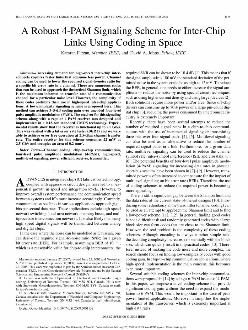
With an additive white Gaussian noise (AWGN) model forthe channel, the 4LINE-PAM4 scheme and the ordinary 4-PAMscheme were simulated in MATLAB. Simulation results showthat the performance of 4LINE-PAM4 scheme is roughly 2.6 dBbetter than the performance of the 4-PAM at symbol error rate(SER) of 10 (see Fig. 7). As shown in Fig. 6(b), the receivercan be also implemented digitally by using 3- or 4-bit analog-to-digital converters (ADCs). Fig. 7 also shows the performance ofthese digital implementations.
B. Simulation Results With a More Realistic Channel Model
AWGN model is a good model for a channel with perfecttermination and no ISI. However, the main sources of the noisein inter-chip applications in practical systems are usually ISI andresidual reflection due to the imperfect termination. Therefore,
Fig. 7. Performance comparison of different schemes.
a more realistic model for the channel [16] is used to verify theperformance of the proposed method in two practical situations.
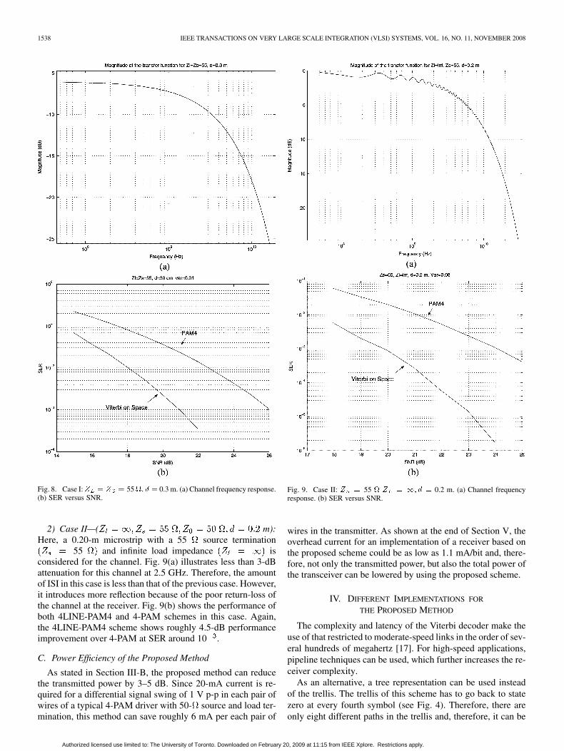
1) Case I—( m): Inthis case, source and load terminations are 10% more than thecharacteristic impedance 50 . A 0.3-m microstrip isconsidered as a medium for this channel. Fig. 8(a) shows themagnitude of the channel transfer function for this channel. Asshown in this figure, the attenuation of the channel is roughly4 dB at 2.5 GHz and, therefore, this channel introduces mod-erate amount of ISI. However, there would be a small residualreflection since the source and load impedances are close to 50(perfect termination). Fig. 8(b), which illustrates the SER vari-ation with SNR for 4LINE-PAM4 and 4-PAM schemes, showsroughly 5-dB gain for the 4LINE-PAM4 scheme.
Authorized licensed use limited to: The University of Toronto. Downloaded on February 20, 2009 at 11:15 from IEEE Xplore. Restrictions apply.
1538 IEEE TRANSACTIONS ON VERY LARGE SCALE INTEGRATION (VLSI) SYSTEMS, VOL. 16, NO. 11, NOVEMBER 2008
Fig. 8. Case I: � � � � 55�� � � 0.3 m. (a) Channel frequency response.(b) SER versus SNR.
2) Case II—( m):Here, a 0.20-m microstrip with a 55 source termination
55 and infinite load impedance isconsidered for the channel. Fig. 9(a) illustrates less than 3-dBattenuation for this channel at 2.5 GHz. Therefore, the amountof ISI in this case is less than that of the previous case. However,it introduces more reflection because of the poor return-loss ofthe channel at the receiver. Fig. 9(b) shows the performance ofboth 4LINE-PAM4 and 4-PAM schemes in this case. Again,the 4LINE-PAM4 scheme shows roughly 4.5-dB performanceimprovement over 4-PAM at SER around 10 .
C. Power Efficiency of the Proposed Method
As stated in Section III-B, the proposed method can reducethe transmitted power by 3–5 dB. Since 20-mA current is re-quired for a differential signal swing of 1 V p-p in each pair ofwires of a typical 4-PAM driver with 50- source and load ter-mination, this method can save roughly 6 mA per each pair of
Fig. 9. Case II: � � 55 � � � �� � � 0.2 m. (a) Channel frequencyresponse. (b) SER versus SNR.
wires in the transmitter. As shown at the end of Section V, theoverhead current for an implementation of a receiver based onthe proposed scheme could be as low as 1.1 mA/bit and, there-fore, not only the transmitted power, but also the total power ofthe transceiver can be lowered by using the proposed scheme.
IV. DIFFERENT IMPLEMENTATIONS FOR
THE PROPOSED METHOD
The complexity and latency of the Viterbi decoder make theuse of that restricted to moderate-speed links in the order of sev-eral hundreds of megahertz [17]. For high-speed applications,pipeline techniques can be used, which further increases the re-ceiver complexity.
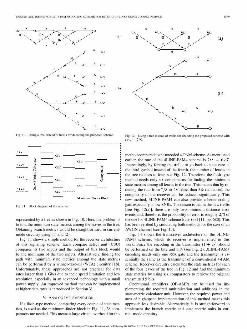
As an alternative, a tree representation can be used insteadof the trellis. The trellis of this scheme has to go back to statezero at every fourth symbol (see Fig. 4). Therefore, there areonly eight different paths in the trellis and, therefore, it can be
Authorized licensed use limited to: The University of Toronto. Downloaded on February 20, 2009 at 11:15 from IEEE Xplore. Restrictions apply.
FARZAN AND JOHNS: ROBUST 4-PAM SIGNALING SCHEME FOR INTER-CHIP LINKS USING CODING IN SPACE 1539
Fig. 10. Using a tree instead of trellis for decoding the proposed scheme.
Fig. 11. Block diagram of the receiver.
represented by a tree as shown in Fig. 10. Here, the problem isto find the minimum state metrics among the leaves in the tree.Obtaining branch metrics would be straightforward in current-mode circuitry using (1) and (2).
Fig. 11 shows a simple method for the receiver architectureof this signaling scheme. Each compare select unit (CSU)compares its two inputs and the output of this block wouldbe the minimum of the two inputs. Alternatively, finding thepath with minimum state metrics amongt the state metricscan be performed by a winner-take-all (WTA) circuitry [18].Unfortunately, these approaches are not practical for datarates larger than 1 Gb/s due to their speed limitation and lowresolution, especially in an advanced technology with a smallpower supply. An improved method that can be implementedat higher data rates is introduced in Section V.
V. ANALOG IMPLEMENTATION
If a flash-type method, comparing every couple of state met-rics, is used as the minimum-finder block in Fig. 11, 28 com-parators are needed. This means a large circuit overhead for this
Fig. 12. Using a tree instead of trellis for decoding the proposed scheme with���� � ���.
method compared to the uncoded 4-PAM scheme. As mentionedearlier, the rate of the 4LINE-PAM4 scheme is .Interestingly, by forcing the trellis to go back to state zero atthe third symbol instead of the fourth, the number of leaves inthe tree reduces to four, see Fig. 12. Therefore, the flash-typemethod needs only six comparators for finding the minimumstate metrics among all leaves in the tree. This means that by re-ducing the rate from to (less than 5% reduction), thecomplexity of the receiver can be reduced significantly. Thisnew method, 3LINE-PAM4 can also provide a better codinggain especially at low SNRs. The reason is that in the new trellis[see Fig. 12(a)], there are only two minimum distance errorevents and, therefore, the probability of error is roughly ofthe one for 4LINE-PAM4 scheme (rate ) [11, pp. 680]. Thishas been verified by simulating both methods for the case of anAWGN channel (see Fig. 13).
Fig. 14 shows the transceiver architecture of the 3LINE-PAM4 scheme, which its receiver is implemented in thiswork. Since the encoding in the transmitter shouldbe performed on the bit2 and bit4 (see Fig. 2), 3LINE-PAM4encoding needs only one XOR gate and the transmitter is es-sentially the same as the transmitter of a conventional 4-PAMscheme. Receiver circuitry calculates the state metrics for eachof the four leaves of the tree in Fig. 12 and find the minimumstate metrics by using six comparators to retrieve the originaltransmitted 5 bits.
Operational amplifiers (OP-AMP) can be used for im-plementing the required multiplication and additions in thestate-metric calculator unit. However, the required power andarea of high-speed implementation of this method makes thisapproach less desirable. Alternatively, it is straightforward toimplement the branch metric and state metric units in cur-rent-mode circuitry.
Authorized licensed use limited to: The University of Toronto. Downloaded on February 20, 2009 at 11:15 from IEEE Xplore. Restrictions apply.

1540 IEEE TRANSACTIONS ON VERY LARGE SCALE INTEGRATION (VLSI) SYSTEMS, VOL. 16, NO. 11, NOVEMBER 2008
Fig. 13. Performance comparison for 4-PAM, 3LINE-PAM4, and the 4LINE-PAM4 scheme.
Fig. 14. Block diagram of the transceiver.
Fig. 15. (a) Block diagram of the receiver. (b) Detail of the state-metric calcu-lator unit.
The detail of receiver architecture for this scheme is shown inFig. 15. The state-metric calculator unit computes the costs forall four paths in the trellis or equivalently for all four leaves inthe tree of Fig. 12. As shown in (1) and (2), calculating the twobranch metrics corresponding to each input line needs two com-parators. Therefore, there would be a total of six comparators inthe state-metric-calculator unit. The detail of this unit is shown
Fig. 16. Detail of the �� � � digital decoder.
in Fig. 15(b). As shown in this figure, the state metric calculatorunit consists of three parts. Each part calculate the branch met-rics, based on (1) and (2), by converting the input signal fromvoltage to current with a transconductance block and performthe branch metrics calculation in current mode using the resultsof the comparator outputs. Calculating the state metrics can bedone by just adding the branch metrics, which would be straight-forward in current mode circuitry. For example, as shown inFig. 15(b), the first state metrics can be generated by simplyadding A1, A2, and A3 (see also Fig. 12).
The outputs of state-metric calculator unit are compared withsix comparators to find the minimum state metrics among thefour leaves in the tree. The original 5 bits can be retrieved fromthe outputs of these comparators and the outputs of the compara-tors in the state-metric calculator unit. These 12 outputs are fedinto a 12 by 5 digital decoder that decodes the original bits in thereceiver. Fig. 16 shows the required circuitry for this decoder.As shown in this figure, the outputs of the first six comparators,which determine the minimum state metrics can be used to re-trieve the second and the fourth transmitted bits, the bits thatdetermine the path in the tree (see Fig. 14). I7 to I12 are the out-puts of the comparators in the state-metric calculator unit thatare used for retrieving the rest of the transmitted bits.
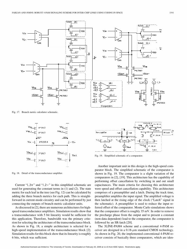
Fig. 17 illustrates the circuit implementation for the branch-metric-calculator unit, which is a direct implementation of (1)and (2) in current mode circuitry. For example, based on (1)
would be either zero or . The right portion of theFig. 17 shows the implementation for this. The output of thetwo transconductance are connected to each other to create the
term in (1) and cascode current mirrors provide the constantterm. The two comparators and the switches in the schematicimplement the conditions in (1) and (2). As shown in this figure,differential pairs are used instead of switches to increase thespeed of this implementation. Also, four transconductance am-plifiers, instead of one, are used for calculating each branchmetric to eliminate the need for current mirrors and, thus, theadditional delay in the signal path.
Authorized licensed use limited to: The University of Toronto. Downloaded on February 20, 2009 at 11:15 from IEEE Xplore. Restrictions apply.
FARZAN AND JOHNS: ROBUST 4-PAM SIGNALING SCHEME FOR INTER-CHIP LINKS USING CODING IN SPACE 1541
Fig. 17. Branch metric calculator schematic.
Fig. 18. Detail of the transconductance amplifier.
Current “ ” and “ ” in this simplified schematic areused for generating the constant terms in (1) and (2). The statemetric for each leaf in the tree (see Fig. 12) can be calculated byadding the three branch metrics for each path. This is straight-forward in current-mode circuitry and can be performed by justconnecting the outputs of branch-metric calculator units.
As discussed in [2], there are numerous architectures for high-speed transconductance amplifiers. Simulation results show thata transconductance with 5 bit linearity would be sufficient forthis application. Therefore, bandwidth was the primary crite-rion for selecting the architecture of the transconductance block.As shown in Fig. 18, a simple architecture is selected for ahigh-speed implementation of the transconductance block [2].Simulation results for this block show that its linearity is roughly6 bits, which was sufficient.
Fig. 19. Simplified schematic of a comparator.
Another important unit in this design is the high-speed com-parator block. The simplified schematic of the comparator isshown in Fig. 19. The comparator is a slight variation of thecomparators in [2], [19]. This architecture has the capability ofperforming offset cancellation by switching in and out smallcapacitances. The main criteria for choosing this architecturewere speed and offset cancellation capability. This architecturecomprises of a preamplifier and a latch. During the track time,preamplifier amplifies the input signal. The amplified voltage isthen latched at the rising edge of the clock (“Latch” signal inthe schematic). A preamplifier is used to reduce the input re-ferred offset of the comparator. Monte Carlo simulations showsthat the comparator offset is roughly 35 mV. In order to removethe precharge phase from the output and to present a constant(non-data dependent) load to the comparator, the comparator isfollowed by an SR-latch [20].
The 3LINE-PAM4 scheme and a conventional 4-PAM re-ceiver are designed in a 0.18- m standard CMOS technology.As shown in Fig. 20, the implemented conventional 4-PAM re-ceiver consists of basically three comparators, which are iden-
Authorized licensed use limited to: The University of Toronto. Downloaded on February 20, 2009 at 11:15 from IEEE Xplore. Restrictions apply.
1542 IEEE TRANSACTIONS ON VERY LARGE SCALE INTEGRATION (VLSI) SYSTEMS, VOL. 16, NO. 11, NOVEMBER 2008
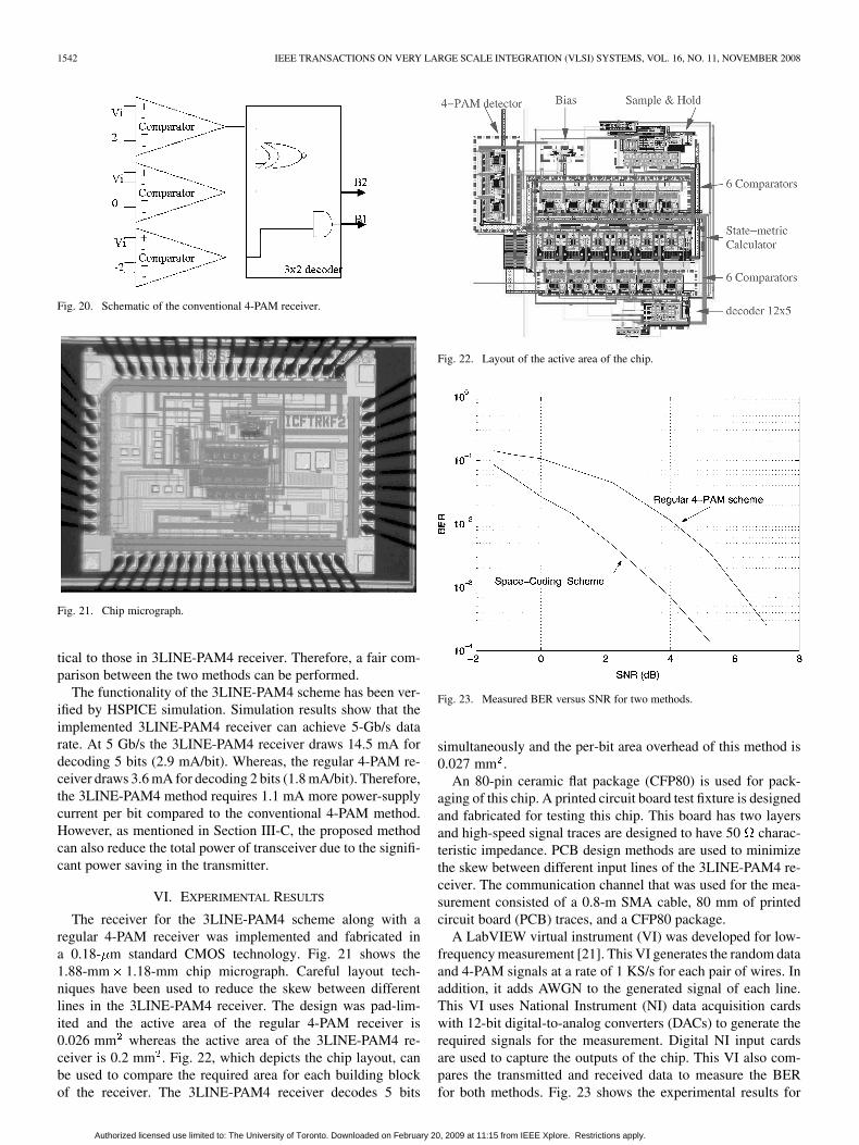
Fig. 20. Schematic of the conventional 4-PAM receiver.
Fig. 21. Chip micrograph.
tical to those in 3LINE-PAM4 receiver. Therefore, a fair com-parison between the two methods can be performed.
The functionality of the 3LINE-PAM4 scheme has been ver-ified by HSPICE simulation. Simulation results show that theimplemented 3LINE-PAM4 receiver can achieve 5-Gb/s datarate. At 5 Gb/s the 3LINE-PAM4 receiver draws 14.5 mA fordecoding 5 bits (2.9 mA/bit). Whereas, the regular 4-PAM re-ceiver draws 3.6 mA for decoding 2 bits (1.8 mA/bit). Therefore,the 3LINE-PAM4 method requires 1.1 mA more power-supplycurrent per bit compared to the conventional 4-PAM method.However, as mentioned in Section III-C, the proposed methodcan also reduce the total power of transceiver due to the signifi-cant power saving in the transmitter.
VI. EXPERIMENTAL RESULTS
The receiver for the 3LINE-PAM4 scheme along with aregular 4-PAM receiver was implemented and fabricated ina 0.18- m standard CMOS technology. Fig. 21 shows the1.88-mm 1.18-mm chip micrograph. Careful layout tech-niques have been used to reduce the skew between differentlines in the 3LINE-PAM4 receiver. The design was pad-lim-ited and the active area of the regular 4-PAM receiver is0.026 mm whereas the active area of the 3LINE-PAM4 re-ceiver is 0.2 mm . Fig. 22, which depicts the chip layout, canbe used to compare the required area for each building blockof the receiver. The 3LINE-PAM4 receiver decodes 5 bits
Fig. 22. Layout of the active area of the chip.
Fig. 23. Measured BER versus SNR for two methods.
simultaneously and the per-bit area overhead of this method is0.027 mm .
An 80-pin ceramic flat package (CFP80) is used for pack-aging of this chip. A printed circuit board test fixture is designedand fabricated for testing this chip. This board has two layersand high-speed signal traces are designed to have 50 charac-teristic impedance. PCB design methods are used to minimizethe skew between different input lines of the 3LINE-PAM4 re-ceiver. The communication channel that was used for the mea-surement consisted of a 0.8-m SMA cable, 80 mm of printedcircuit board (PCB) traces, and a CFP80 package.
A LabVIEW virtual instrument (VI) was developed for low-frequency measurement [21]. This VI generates the random dataand 4-PAM signals at a rate of 1 KS/s for each pair of wires. Inaddition, it adds AWGN to the generated signal of each line.This VI uses National Instrument (NI) data acquisition cardswith 12-bit digital-to-analog converters (DACs) to generate therequired signals for the measurement. Digital NI input cardsare used to capture the outputs of the chip. This VI also com-pares the transmitted and received data to measure the BERfor both methods. Fig. 23 shows the experimental results for
Authorized licensed use limited to: The University of Toronto. Downloaded on February 20, 2009 at 11:15 from IEEE Xplore. Restrictions apply.

FARZAN AND JOHNS: ROBUST 4-PAM SIGNALING SCHEME FOR INTER-CHIP LINKS USING CODING IN SPACE 1543
Fig. 24. Typical eye-diagram for the single-ended receiver input signal.
BER-versus-SNR measurements using this VI. As shown inFig. 23, the performance of the 3LINE-PAM4 scheme is roughly2.3 dB better than that of the regular 4-PAM receiver, which issimilar to the simulation results for an AWGN channel. This canbe expected since at low-speed an AWGN model is a good ap-proximation for the channel.
The functionality of 3LINE-PAM4 scheme at higher datarates (up to 2.5 Gb/s) was verified by a parallel bit error ratiotester (ParBERT). The receiver’s input signals were generatedby combining the output of two channels of ParBERT bya splitter/combiner. Fig. 24 shows a typical eye-diagram ofa single-ended receiver input (splitter/combiner output). Asshown in this figure, the single-ended signal level are: 450, 550,650, and 750 mV. Therefore, the differential signal levels are:
100 and 300 mV. The retrieved outputs of the chip werefed back to the ParBERT input to measure the BER.
Ideally, we need a high-speed arbitrary waveform generatorwith four channels in order to generate high-speed 4-PAM sig-nals superimposed by additive white Gaussian noise for BERversus SNR measurement of this chip. Unfortunately, due to thelack of the required equipment, the measurement of noise per-formance was not feasible at high data rates. However, experi-mental results at 900 Mb/s show that the 3LINE-PAM4 schemeneeds a smaller SNR for a given performance. For example, re-ducing the signal swing by 10% and 20% results in BERs of
and , respectively, for 4-PAM and BERs ofand for 3LINE-PAM4.
Experimental results show that the 3LINE-PAM4 receivercan function with zero error rate up to 2.5 Gb/s. It should bementioned that simulation results show that the 3LINE-PAM4
TABLE ICOMPARISON BETWEEN SIMULATION AND EXPERIMENTAL RESULTS
receiver could work error free up to 5 Gb/s and the 2.5-Gb/sspeed limitation is mainly due to the lack of proper equipmentand skew compensation. Finally, the 3LINE-PAM4 receiverdraws roughly 12 mA from a 1.8-V power supply at 2.5 Gb/s.This is in agreement with the simulated power at this speedwhich is 11.5 mA at 2.5 Gb/s. Simulation results show that thethe current consumption increases to only 14.5 mA at 5 Gb/s.Table I summarizes the simulation and measurement results.As shown in this table, there is a good agreement between thesimulation and measurement for low-frequency performanceimprovement of the proposed method.
VII. CONCLUSION
Multilevel signaling can be used to reduce the number ofsignal paths or to increase the data rate. Two coding schemes,4LINE-PAM4 and 3LINE-PAM4, that can reduce the trans-mitted power of multilevel signaling have been introduced.These coding schemes have roughly 3–5 dB coding gain overthe uncoded 4-PAM. Although more complex coding schemescan be used to achieve higher coding gain, the high-speed im-plementation is an important factor that should be consideredwhen developing coding schemes for high-speed interconnect.Moreover, analog implementations of the proposed methods
Authorized licensed use limited to: The University of Toronto. Downloaded on February 20, 2009 at 11:15 from IEEE Xplore. Restrictions apply.

1544 IEEE TRANSACTIONS ON VERY LARGE SCALE INTEGRATION (VLSI) SYSTEMS, VOL. 16, NO. 11, NOVEMBER 2008
have been presented. The proposed low-complexity analogimplementation of 3LINE-PAM4 makes its high-speed im-plementation feasible. This 3LINE-PAM4 scheme is designedand implemented in a 0.18- m standard CMOS technology.This coding scheme transmits 5 bits over 3 differential lines of4-PAM resulting in a code rate. Experimental results notonly verified the coding gain at low-speed, but also showedthat the chip is functional up to 2.5 Gb/s. The measured supplycurrent for the proposed method was 12.5 mA at 2.5 Gb/sand the active area of the implemented receiver based on thismethod was 0.2 mm .
REFERENCES
[1] W. J. Dally and J. W. Poulton, Digital Systems Engineering.. Cam-bridge, U.K.: Cambridge University Press, 2000.
[2] D. A. Johns and K. W. Martin, Analog Integrated Circuit Design..New York: Wiley, 1997.
[3] N. Tan and S. Eriksson, “Low-power chip-to-chip communication cir-cuits,” Electron. Lett., vol. 30, pp. 1732–1733, Oct. 1994.
[4] A. Carusone, K. Farzan, and D. Johns, “Differential signaling with areduced number of signal paths,” IEEE Trans. Circuits Syst. II, Exp.Briefs, vol. 48, no. 3, pp. 294–300, Mar. 2001.
[5] S.-W. Choi, H.-B. Lee, and H.-J. Park, “A three-data differential sig-naling over four conductors with pre-emphasis and equalization: ACMOS current mode implementation,” IEEE J. Solid-State Circuits,vol. 41, no. 3, pp. 633–641, Mar. 2006.
[6] D. J. Foley and M. P. Flynn, “A low-power 8-PAM serial transceiver,”IEEE J. Solid-State Circuits, vol. 37, no. 3, pp. 310–316, Mar. 2002.
[7] J. L. Zerbe et al., “1.6 Gb/s/pin 4-PAM signaling and circuits for amultidrop bus,” in Proc. IEEE VLSI Symp. Circuits, Jun. 2000, pp.128–131.
[8] R. Farjad-Rad, C.-K. K. Yang, M. A. Horowitz, and T. H. Lee, “A 0.4�m CMOS 10-Gb/s 4-PAM pre-emphasis serial link,” IEEE J. Solid-State Circuits, vol. 34, no. 5, pp. 580–585, May 1999.
[9] R. Farjad-Rad, C.-K. K. Yang, and M. A. Horowitz, “A 0.3 �m CMOS8-Gb/s 4-PAM serial link transceiver,” IEEE J. Solid-State Circuits, vol.35, no. 5, pp. 757–764, May 2000.
[10] M. V. Ierssel, T. Esmailian, A. Sheikholeslami, and S. Pasupathy, “Sig-naling capacity of FR4 PCB traces for chip-to-chip communication,” inProc. IEEE Int. Symp. Circuit Syst. (ISCAS), May 2003, pp. V85–V88.
[11] E. A. Lee and D. G. Messerschmit, Digital Communication.. Nor-well, MA: Kluwer, 1994.
[12] K. Farzan and D. A. Johns, “Power-efficient chip-to-chip signalingschemes,” in Proc. IEEE Int. Symp. Circuit Syst. (ISCAS), May 2002,pp. II-560–II-563.
[13] S. Benedetto, G. Montorsi, and D. Divsalar, “Concatenated convolu-tional codes with interleavers,” IEEE Commun. Mag., vol. 41, no. 8,pp. 102–108, Aug. 2003.
[14] K. Farzan and D. A. Johns, “Coding schemes for chip-to-chip intercon-nects,” IEEE Trans. Very Large Scale Integr. (VLSI) Syst., vol. 14, no.4, pp. 393–406, Apr. 2006.
[15] M. Hatamian, O. E. Agazzi, J. Creigh, H. Samueli, A. J. Castellano,D. Kruse, A. Madisetti, N. Yousefi, K. Bult, P. Pai, M. Wakayama, M.M. McConnell, and M. Colombatto, “Design consideration for gigabitethernet 1000Base-T twisted pair transceivers,” in Proc. IEEE CustomIntegr. Circuits Conf. (CICC), May 1998, pp. 335–342.
[16] K. Farzan and D. A. Johns, “A low-complexity power-efficient sig-naling scheme for chip-to-chip communication,” in Proc. IEEE Int.Symp. Circuit Syst. (ISCAS), May 2003, pp. V-77–V-80.
[17] M. H. Shakiba, D. A. Johns, and K. W. Martin, “Bicmos circuits foranalog viterbi decoders,” IEEE Trans. Circuits Syst. II, Exp. Briefs, vol.45, no. 12, pp. 1527–1537, Dec. 1998.
[18] S. Vlassis and S. Siskos, “High-speed and high-resolution WTA cir-cuit,” in Proc. IEEE Int. Symp. Circuit Syst. (ISCAS), May 1999, pp.224–227.
[19] M. E. Lee, W. J. Dally, and P. Chiang, “Low-power area-efficient high-speed I/O circuit techniques,” IEEE J. Solid-State Circuits, vol. 35, no.11, pp. 1591–1599, Nov. 2000.
[20] C.-K. Yang, V. Stojanovic, S. Modjtahedi, M. Horowitz, and W. Eller-sick, “A serial-link transceiver based on 8-GSample/s A/D and D/Aconverters in 0.25 �m digital CMOS,” IEEE J. Solid-State Circuits,vol. 36, no. 11, pp. 1684–1692, Nov. 2001.
[21] National Instrument, “Graphical development software,” 2006. [On-line]. Available: http://www.ni.com/labview
Kamran Farzan (S’01–M’05) was born in Isfahan,Iran, in 1971. He received the B.A.Sc. degree from Is-fahan University of Technology (IUT), Isfahan, Iran,in 1994, the M.A.Sc. degree from the University ofTehran, Tehran, Iran, in 1997, and the Ph.D. degreein the area of high-speed chip-to-chip communicationfrom University of Toronto, Toronto, ON, Canada, in2004.
He has been with Snowbush Microelectronicssince 2003, where he works in the area of analogdesign for high-speed transmitter/receiver and read
channel analog front end. From 1994 to 1995, he worked with the Electricaland Computer Engineering Research Center (ECERC), IUT. From 1997 to1999, he worked with ECERC as a Senior Researcher in the area of digitalsignal processing.
Dr. Farzan was the recipient of the Inventors Recognition Awards of Semicon-ductor Research Corporation (SRC) and the 2003 Analog Devices OutstandingStudent Designer Award.
David A. Johns (S’81–M’89–SM’94–F’01) receivedthe B.A.Sc., M.A.Sc., and Ph.D. degrees from theUniversity of Toronto, Toronto, ON, Canada, in 1980,1983, and 1989, respectively.
In 1988, he was hired at the University of Toronto,where he is currently a Full Professor. He has on-going research programs in the general area of analogintegrated circuits with particular emphasis on digitalcommunications. His research work has resulted inmore than 40 publications. His is coauthor of the text-book Analog Integrated Circuit Design (Wiley, 1997)
and has given numerous industrial short courses. Together with academic expe-rience, he also has spent a number of years in the semiconductor industry andis a cofounder of Snowbush Microelectronics.
Dr. Johns was a recipient of the 1999 IEEE Darlington Award. He served as aGuest Editor of the IEEE JOURNAL OF SOLID-STATE CIRCUITS and an AssociateEditor for the IEEE TRANSACTIONS ON CIRCUITS AND SYSTEMS—II: EXPRESS
BRIEFS from 1993 to 1995 and for IEEE TRANSACTIONS ON CIRCUITS AND
SYSTEMS—I: EXPRESS BRIEFS from 1995 to 1997 and was elected to Adcom forSSCS in 2002. His homepage is located at http://www.eecg.toronto.edu/~johns.
Authorized licensed use limited to: The University of Toronto. Downloaded on February 20, 2009 at 11:15 from IEEE Xplore. Restrictions apply.