Embed Size (px)
Citation preview

IEEE TRANSACTIONS ON VERY LARGE SCALE INTEGRATION (VLSI) SYSTEMS, VOL. 14, NO. 5, MAY 2006 501
HotSpot: A Compact Thermal Modeling Methodologyfor Early-Stage VLSI Design
Wei Huang, Student Member, IEEE, Shougata Ghosh, Siva Velusamy, Karthik Sankaranarayanan,Kevin Skadron, Senior Member, IEEE, and Mircea R. Stan, Senior Member, IEEE
Abstract—This paper presents HotSpot—a modeling method-ology for developing compact thermal models based on the pop-ular stacked-layer packaging scheme in modern very large-scaleintegration systems. In addition to modeling silicon and pack-aging layers, HotSpot includes a high-level on-chip interconnectself-heating power and thermal model such that the thermalimpacts on interconnects can also be considered during earlydesign stages. The HotSpot compact thermal modeling approachis especially well suited for preregister transfer level (RTL) andpresynthesis thermal analysis and is able to provide detailed staticand transient temperature information across the die and thepackage, as it is also computationally efficient.
Index Terms—Compact thermal model, early design stages, in-terconnect self-heating, temperature, VLSI.
I. INTRODUCTION
AN unfortunate side effect of miniaturization and the con-tinued scaling of CMOS technology is the ever-increasing
power densities. The resulting difficulties in managing temper-atures, especially local hot spots, have become one of the majorchallenges for designers at all design levels. High temperatureshave several significant impacts on VLSI systems. First, thecarrier mobility is degraded at higher temperature, resulting inslower devices. Second, leakage power is escalated due to theexponential increase of subthreshold current with temperature.Third, the interconnect resistivity increases with temperature,leading to worse power-grid IR drops and longer interconnectRC delays, hence causing performance loss and complicatingtiming and noise analysis. Finally, elevated temperatures canshorten interconnect and device life times and package relia-bility can be severely affected by local hot spots and highertemperature gradients. For all of these reasons, in order to fullyaccount for the thermal effects, it is important to model temper-ature for VLSI systems in an accurate but still efficient way. For
Manuscript received November 26, 2004; revised July 19, 2005, andNovember 13, 2006. This work was supported in part by the National ScienceFoundation under Grants CCR-0133634 and CCF-0429765, two grants fromIntel MRL, and by the University of Virginia through the FEST ExcellenceAward.
W. Huang and M. R. Stan are with the Charles L. Brown Department of Elec-trical and Computer Engineering, University of Virginia, Charlottesville, VA22904 USA (e-mail: [email protected]; [email protected]).
S. Ghosh was with the University of Virginia, Charlottesville, VA 22904USA. He is now with the Department of Electrical Engineering, Princeton Uni-versity, Princeton, NJ 08544 USA (e-mail: [email protected]).
S. Velusamy was with the University of Virginia, Charlottesville, VA 22904USA. He is now with Xilinx Inc., San Jose, CA 95124 USA.
K. Sankaranarayanan and K. Skadron are with the Department of ComputerScience, University of Virginia, Charlottesville, VA 22904 USA (e-mail:[email protected]; [email protected]).
Digital Object Identifier 10.1109/TVLSI.2006.876103
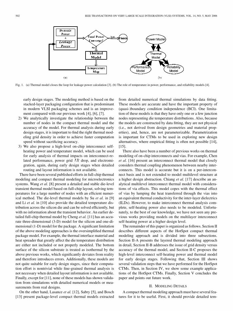
example, knowing the across-die temperature distribution at de-sign time permits thermally self-consistent leakage power calcu-lations in an iterative manner, as shown in Fig. 1(a) [1]–[3]. Sim-ilarly, an efficient thermal model can also help to close the loopfor temperature-aware performance and reliability analysis, assuggested in Fig. 1(b). In particular, it is crucial to take thermaleffects into account as early as possible in the design flow, be-cause optimal early and high-level thermally related design de-cisions can significantly improve design efficiency and reducedesign cost.
Obviously, it is impractical to accurately analyze thermaleffects and model temperature distribution of a system togetherwith the environment in their full details. Using numericalthermal analysis methods, such as the finite-element method(FEM), is a time-consuming process not suitable for de-sign-time and run-time thermal analysis. In order to gain moreinsights of the thermal effects during early IC design stages, thetradeoff solution is to build compact thermal models (CTMs)that give reasonably accurate temperature predictions with littlecomputational effort at desired levels of abstraction [5]. Earlydesign stages present unique challenges that we believe requirea by-construction compact modeling approach.
Based on the well-known duality between thermal and elec-trical phenomena,1 a CTM is a lumped thermal RC network,with heat dissipation modeled as current sources. The resultingthermal RC networks are typically relatively small, can besolved for temperature very efficiently and introduce littlecomputational overhead. Due to this computational efficiency,at pre-register transfer level (RTL) and presynthesis designstages, it is desirable to have compact thermal models forboth temperature-aware design and fast simulations of archi-tecture-level dynamic thermal management techniques. Here,temperature-aware design refers to a design methodology thatuses temperature as a guideline throughout the design flow. Theresulting design can thus be thermally optimized, as it takesinto account potential thermal limitations [4].
The major contributions of this work are the following.1) We propose a modeling methodology—HotSpot—for gen-
erating CTMs that can be used in early VLSI design stageswhere detailed layout is not available. With this method,reasonably accurate spatial and temporal temperature vari-ations of the silicon die as well as the package can bequickly obtained to help efficient design decisions during
1In this duality, the heat flow passing through a thermal resistance is analo-gous to electrical current, and the temperature difference is analogous to voltage.Thermal capacitance, which is based on the material’s specific heat and definingthe heat absorbing capability, is analogous to electrical capacitance which ac-cumulates electrical charge.
1063-8210/$20.00 © 2006 IEEE
502 IEEE TRANSACTIONS ON VERY LARGE SCALE INTEGRATION (VLSI) SYSTEMS, VOL. 14, NO. 5, MAY 2006
Fig. 1. (a) Thermal model closes the loop for leakage power calculation [3]. (b) The role of temperature in power, performance, and reliability models [4].
early design stages. The modeling method is based on thestacked-layer packaging configuration that is predominantin modern VLSI packaging schemes and is an improve-ment compared with our previous work [4], [6], [7].
2) We analytically investigate the relationship between thenumber of nodes in the compact thermal model and theaccuracy of the model. For thermal analysis during earlydesign stages, it is important to find the right thermal mod-eling grid density in order to achieve faster computationspeed without sacrificing accuracy.
3) We also propose a high-level on-chip interconnect self-heating power and temperature model, which can be usedfor early analysis of thermal impacts on interconnect-re-lated performance, power grid drop, and electromi-gration, again, during early design stages when detailedrouting and layout information is not available.
There have been several published efforts in full-chip thermalmodeling and compact thermal modeling for microelectronicssystems. Wang et al. [8] present a detailed and stable die-leveltransient thermal model based on full-chip layout, solving tem-peratures for a large number of nodes with an efficient numer-ical method. The die-level thermal models by Su et al. in [9]and Li et al. in [10] also provide the detailed temperature dis-tribution across the silicon die and can be solved efficiently, butwith no information about the transient behavior. An earlier de-tailed full-chip thermal model by Cheng et al. [11] has an accu-rate three-dimensional (3-D) model for the silicon and one-di-mensional (1-D) model for the package. A significant limitationof the above modeling approaches is the oversimplified thermalpackage model. For example, the thermal interface material andheat spreader that greatly affect the die temperature distributionare either not included or not properly modeled. The bottomsurface of the silicon substrate is treated as isothermal by theabove previous works, which significantly deviates from realityand therefore introduces errors. Additionally, these models arenot quite suitable for early design stages, since their computa-tion effort is nontrivial while fine-grained thermal analysis isnot necessary when detailed layout information is not available.Finally, except for [11], none of these models has shown valida-tion from simulations with detailed numerical models or mea-surements from real designs.
On the other hand, Lasance et al. [12], Sabry [5], and Bosch[13] present package-level compact thermal models extracted
from detailed numerical thermal simulations by data fitting.These models are accurate and have the important property of(quasi-)boundary condition independence (BCI). One limita-tion of these models is that they have only one or a few junctionnodes representing die temperature distributions. Also, becausethe models are constructed by data fitting, they are not physical(i.e., not derived from design geometries and material prop-erties), and, hence, are not parameterizable. Parametrizationis important for CTMs to be used in exploring new designalternatives, where empirical fitting is often not possible [14],[15].
There also have been a number of previous works on thermalmodeling of on-chip interconnects and vias. For example, Chenet al. [16] present an interconnect thermal model that closelyconsiders thermal coupling phenomenon between nearby inter-connects. This model is accurate but it is on a per-intercon-nect basis and is not extended to model multilevel structure ata higher design abstraction. Chiang et al. [17] describe an an-alytical multilevel interconnect thermal model with considera-tions of via effects. This model copes with the thermal effectof vias by lumping the heat transferred through the vias intoan equivalent thermal conductivity for the inter-layer dielectrics(ILDs). However, to make interconnect thermal analysis com-plete, self-heating power also needs to be modeled. Unfortu-nately, to the best of our knowledge, we have not seen any pre-vious works providing models on the multilayer interconnectself-heating power at a higher design level.
The remainder of this paper is organized as follows. Section IIdescribes different aspects of the HotSpot compact thermalmodeling approach and is divided into three subsections.Section II-A presents the layered thermal modeling approachin detail, Section II-B addresses the issue of grid density versusaccuracy of the thermal model, and Section II-C proposes thehigh-level interconnect self-heating power and thermal modelfor early design stages. Following that, Section III showsseveral validation steps that we have performed for the HotSpotCTMs. Then, in Section IV, we show some example applica-tions of the HotSpot CTMs. Finally, Section V concludes thepaper and points out future work.
II. MODELING DETAILS
A compact thermal modeling approach must have several fea-tures for it to be useful. First, it should provide detailed tem-

HUANG et al.: HOTSPOT: A COMPACT THERMAL MODELING METHODOLOGY 503
Fig. 2. Stacked layers in a typical ceramic ball grid array (CBGA) package [18]
perature distribution at the desired level of abstraction (e.g., asingle node representing the die temperature is unacceptable forthermal modeling at the IC level). In addition, both static andtransient thermal behavior should be modeled. Second, a CTMshould model just at the needed accuracy and hide the details oflower levels, so that the model itself is no more complex thannecessary. Third, the model structure should be kept as simpleas possible and should introduce little computational overhead.The HotSpot compact thermal modeling methodology proposedin this paper has all of the above desired features.
A. General Methodology
Most modern VLSI systems have a package consisting ofseveral stacked layers made of different materials, as shown inFig. 2. This is also the package scheme adopted for the HotSpotthermal models used in this paper. Typical layers include heatsink, heat spreader, thermal paste, silicon substrate, on-chip in-terconnect layers, C4 pads, ceramic packaging substrate, andsolder balls. The recently proposed stacked chip-scale pack-aging (SCP) [19] and 3-D IC designs [20] are also stacked-layerstructures and can be easily modeled as extensions of the genericstack structure in Fig. 2.
When deriving a compact thermal model in HotSpot, the dif-ferent layers, their positions and adjacency are first identified.Each layer is then divided into a number of blocks. For example,in Fig. 3(c), the silicon substrate layer is divided according toarchitecture-level units or into regular grid cells, depending onwhat the die-level design requires. Note that only three blocksare shown in Fig. 3(c) for simplicity. Other layers that greatlyaffect across-die temperature distribution (e.g., thermal inter-face material) can be modeled similarly to the silicon substrate.For the analysis of the needed size of regular grid cells, seeSection II-B.
For other layers that require less detailed thermal information(such as heat spreader and heat sink), we simply divide that layeras illustrated in Fig. 3(a). The center shaded part in a layer shownby Fig. 3(a) is the area covered by another adjacent layer such asthe one shown in Fig. 3(c). This center part can have the samenumber of nodes as its smaller neighbor layer or can collapsethose nodes into fewer nodes, depending on the accuracy and
Fig. 3. (a) Partitioning of large-area layers (top view). (b) One block with itslateral and vertical thermal resistances (side view). (c) A layer, for example, thesilicon die, can be divided into an arbitrary number of blocks if detailed thermalinformation is needed (top view).
computation speed requirements. The remaining peripheral partin Fig. 3(a) is then divided into four trapezoidal blocks, eachassigned to one node.
Every block or grid cell in each layer has one vertical thermalresistance connected to the next layer and several lateral re-sistances to its neighbors in the same layer. Fig. 3(b) shows aside view of one block with both the lateral and the verticalthermal resistances. The vertical thermal resistance is calculatedby , where is the thickness of that layer,is the thermal conductivity of the material of that layer, andis the cross-sectional area of the block. We see that each layer isnot further divided into multiple thinner layers in the vertical di-rection, i.e., our modeling method is not fully 3-D. This is a rea-sonable approximation for early design stages since each layeris relatively thin (a millimeter or less), further discretization inthe vertical direction would induce more computation while notimproving accuracy significantly.
Calculating lateral thermal resistance is not as straightfor-ward as the vertical resistance. This is because heat spreadingor constriction in the lateral directions must be accounted for.Basically, the lateral thermal resistance on one side of a block

504 IEEE TRANSACTIONS ON VERY LARGE SCALE INTEGRATION (VLSI) SYSTEMS, VOL. 14, NO. 5, MAY 2006
can be considered as the spreading/constriction thermal resis-tance of the neighboring part within a layer to that specific block.Lateral thermal resistances are normally much greater than theirvertical counterparts due to the fact that the lateral heat-transfercross-sectional areas are usually much less than vertical ones.We calculate the spreading/constriction resistance based on theformulas given in [21]. The resistance is a spreading one if thelateral area of the source is smaller than the bulk lateral area,and it is a constriction one otherwise.
For each node, there is also a thermal capacitance, connected to ground, where and are the spe-
cific heat and density of the material, respectively. The factoris a scaling factor accounting for lumped versus dis-
tributed thermal time constants.2
Finally, the heatsink-to-air convection thermal resistance canbe modeled as , where is the surfacearea and is the heat transfer coefficient that is boundary condi-tion dependent. For a first-order approximation, this is adequatefor thermal analysis during early design stages. Typical valuesof for typical heat sinks under different convection conditionsusually be found in the heat sink datasheets.
Details of the derivations and formulas of all the abovethermal resistances and capacitances can be found in [7] and[21]. An example of how a HotSpot compact thermal model isassembled can be found in [4].
From the above descriptions, it can be seen that our methodcan model relatively detailed static and transient temperaturevariations for the silicon die. In particular, different packagingcomponents can be modeled with more detailed temperaturedistribution information, which is not available in existingworks such as [8]–[10]. Additionally, because the thermalmodels are built as lumped thermal RC networks, the com-putational overhead for solving the temperatures is small.Therefore, the modeling method is suitable for developingcompact thermal models used during early design stages.
Compact thermal models developed from this method are alsoparameterizable and BCI. The models are parameterizable be-cause they are built only using the physical geometries and ma-terial properties. The models are also BCI because the entire in-ternal RC network is built independent of boundary conditions.More discussions on parametrization and BCI of the HotSpotmodels can be found in [14] and [15].
B. Thermal Modeling Accuracy Analysis
One important aspect of model development is to decide theproper number of nodes at which temperatures are modeled. Atone extreme, a single junction temperature for the chip wouldbe enough for board-level designs, but not enough for die-leveldesigns. Taking the die-level temperature modeling as an ex-ample, temperature can be modeled at the functional unit level[see Fig. 4(a)] or the die can be divided into regular grid cells toget more detailed temperature distribution as a function of thesize of each grid cell [see Fig. 4(b)]. Ideally, we would prefer
2There should be no surprise that the same factor also appears in the analysisof distributed RC electrical interconnect lines. This approximation is legitimatesince the lateral thermal resistances are usually much greater and make negli-gible contribution to the thermalRC time constants compared with the verticalthermal resistances.
Fig. 4. Modeling at the granularity of (a) functional blocks, (b) uniform gridcells, and (c) hybrid-sized grid cells [2].
Fig. 5. (a) A 1-D slab of material with left half dissipating power. (b) Temper-ature distribution along the length of the slab.
a hybrid grid scheme that combines both the per-function unitmodel and the uniform-size grid model as in Fig. 4(c) [2]. Bydoing this, we could still get detailed thermal information forparticular blocks under consideration while saving computa-tion effort by introducing fewer nodes inside other blocks. Itis clear that the desired accuracy determines the minimum gridcell size needed, i.e., the temperature difference across one gridcell should be less than a certain percentage of the maximumtemperature difference across the die. In what follows, we showan analytical method to derive the proper size of a grid cell.
Let us first start from a simple case. Assume that there is a slabof material with unit width and infinite length. The thickness ofthe slab is , and the bottom surface of the slab is isothermal.Half of the slab has a uniform power density of , while thepower density of the other semi-infinite half is , as shown inFig. 5(a). The resulting temperature distribution of the top sur-face of the slab is approximated in Fig. 5(b). The far end of theleft half with power density has a temperature of , andthe far end of the right half with no power dissipated has a tem-perature of , for simplicity. Due to symmetry, the temperatureat the boundary between the two halves is . The temper-ature at point can then be derived from the equivalent lumpedthermal circuit in Fig. 6(a). The lateral and vertical thermal re-sistances of an infinitesimal portion of the slab with length of
are
and (1)
where is the thermal conductivity of the slab material. Now,the equivalent thermal resistance for the semi-infinite half ofthe slab should be the same whether or not it includes the firstvertical thermal resistance , i.e.,
and also
(2)

HUANG et al.: HOTSPOT: A COMPACT THERMAL MODELING METHODOLOGY 505
Fig. 6. (a) Thermal resistance network for Fig. 5(a). (b) Thermal circuit at node x for calculating temperature T (x).
Solving the above two equations for leads to
(3)
When , we have and should have a finite value,which means we can neglect the term in the above twoequations of . Therefore, both equations become
i.e., (4)
Next, to find the temperature , we consider the circuit inFig. 6(b), in which heat flows into node . According toKirchoff’s Current Law, we have
(5)
Substituting with , and with , and then rear-ranging both sides of the equation, we obtain
(6)
Taking the integral for both sides from to andfrom to , respectively, and solving for , we obtain
(7)
The above equation shows that the temperature distribution forthe right half of the slab is approximately an exponential decaycurve with a “spatial” constant of , which is the thickness fromthe surface under consideration to the isothermal surface. Fur-thermore, we can write the temperature distribution of the lefthalf of the slab as a function of position according to symmet-rical nature of the slab structure
(8)
Fig. 7. Comparing FEM simulation result with (7) and (8) for the structure inFig. 5(a). Power density = 0:5 W/mm ; t � 20 mm. Bottom surface of thesilicon slab is approximately isothermal.
Fig. 7 confirms the accuracy of the above analysis by comparingwith FEM simulations using FloWorks.3
Next, we consider the scenario where heat is dissipated on afinite part of the slab, as shown in Fig. 8(a). The correspondingFEM-simulated temperature distributions within that part of theslab are shown in Fig. 8(b) for different block sizes .It is obvious in Fig. 8(b) that, if the size is sufficiently small, theheated part of slab does not actually reach its maximum tem-perature, as can be seen in Fig. 5(b). This is due to the abovementioned spatial constant, and it means that a block with smallsize acts as a temperature-spatial low-pass “filter” that preventsthe temperature from reaching the maximum possible value.In contrast, with the same power density, a bigger block withits size much larger than the “spatial” constant can have sig-nificantly higher temperature differences. The above analysisexplains the “abnormal“ observations that although, some tinystructures such as clock buffers in a microprocessor have veryhigh power densities, they do not necessarily cause hot spots,due to this “spatial temperature filtering“ effect.
For a particular grid size , from (8) and Fig. 8(b), the tem-perature difference within the grid is
(9)
3FloWorks is an FEM software analyzing computational fluid dynamics andheat transfer. Available at http://www.nika.biz/index2.htm

506 IEEE TRANSACTIONS ON VERY LARGE SCALE INTEGRATION (VLSI) SYSTEMS, VOL. 14, NO. 5, MAY 2006
Fig. 8. (a) Part of the slab of material dissipating power. The size of the part is w. (b) FEM simulation results—temperature distribution along the slab withdifferent sizes dissipating power (w < w ). Smaller size “filters” out the temperature difference. (Silicon thickness t = 20 mm.)
By setting
% (10)
where % is the tolerable percentage error, and now rep-resents the maximum possible temperature difference across thesilicon die.4 Solving (10), we get the lower bound for as
%(11)
Note that , which is the thickness from the surface under con-sideration to the isothermal surface, needs to be calculated first.An isothermal surface is an ideal concept that is not found inreal packages, but surfaces with negligible temperature differ-ences can be considered as isothermal.5 For instance, the thick-ness for the silicon surface of the package shown in Fig. 2 canbe found by adding up the thickness of silicon substrate, thermalinterface material, and heat spreader. An important detail is that,if we use the conductivity of silicon in the above equations, weneed to first convert the actual thicknesses of the thermal inter-face material and the heat spreader to “equivalent“ silicon thick-ness by multiplying their thickness by the ratio of their thermalconductivities to the one for silicon.
Fig. 9 plots the required grid size for different desired levelsof precision according to (11), with equivalent thicknesses
mm and mm. The horizontal axis is the ratio ofto , i.e., , in percentage. For example, consider that wehave a 20 mm 20 mm silicon die, and the maximum possibletemperature difference across the die is 30 , then, from Fig. 9,we can find that, if we desire all grid temperature error of lessthan 3% ( % ) for mm, a grid size of approx-imately 0.5 mm is sufficient. This corresponds to dividing the
4T is dependent on the power distribution across the die and cannot beknown a priori without performing thermal analysis. However, one can alwaysstart with a reasonable guessed value for T based on previous design expe-rience and then solve the thermal model and iterate the analysis in Section II-Bfor a few times to get the needed grid size.
5One example is the bottom surface of the heat spreader, since the heatspreader is usually made of materials with high thermal conductivity, such ascopper.
Fig. 9. Minimum necessary grid size for different desired levels of precision,with t = 4 mm and t = 2 mm, respectively. The X-axis is the ratio of �Tto T , i.e., p, in percentage. For example, for a system with t = 4 mm, if3% temperature precision is desired, from the solid line, one finds that a gridcell size of 0.5 mm would be enough.
die into 40 40 grid cells. Any finer grid size is unnecessary inthis case.6
One assumption that we have made so far is that the power isuniform within each grid cell. This assumption is legitimate ifthe thermal analysis is performed at early design stages, becausedetailed layout and power information are not available yet. Inlater design stages, the structures that are included in one gridcell may turn out to be heterogenous. In this case, we can alwaysfirst resort to finer grid cells inside which power distribution canbe considered as uniform, then perform the above accuracy anal-ysis and decide whether or not that finer grid size is necessary ornot. Due to the “spatial temperature filtering effect“ mentionedabove, often we should find that temperature difference withina finer grid cell is negligible and we need to come back to largergrid cells, unless the power density is extremely high.
6It is worth noting that the above granularity analysis is based on simplifi-cations of classical heat transfer equations, which underestimates temperaturewhen applied at size scales less than the phonon–phonon mean free path (about300 nm for silicon at room temperature) [22]. Thus, for granularity analysis atthe transistor level, the phonon Boltzmann transport equation (BTE) should beused instead.

HUANG et al.: HOTSPOT: A COMPACT THERMAL MODELING METHODOLOGY 507
Fig. 10. (a) An example of wire-length distribution at 45nm technology node, with three regions (local, semi-global, and global). (b) Metal-layer assignment bycalculating number of metal layers needed for each of the three regions. (c) Metal-layer assignment by filling every two metal layers with signal wires, startingfrom Metal 1 and Metal 2. The example in (c) is superior to that given in (b) by providing more detailed metal-layer assignment information.
C. Interconnect Self-Heating Power and Thermal Modeling
There are two major heat transfer paths inside an IC package[18]—a primary heat transfer path (e.g., silicon substrate, heatspreader, or heat sink) and a secondary heat transfer path (e.g.,silicon substrate, on-chip interconnect layers, C4 pads, ceramicpackaging substrate, solder balls, or printed circuit board). Onthe other hand, the secondary heat transfer path usually removesa nonnegligible amount of total generated heat (up to 30%).Neglecting the secondary heat transfer path can lead to inac-curate temperature predictions. In addition, as part of the sec-ondary heat transfer path, the on-chip interconnect layers are ofparticular interest, because interconnect temperature informa-tion allows designers to perform more accurate electromigra-tion, wire delay, and IR drop analysis. Until now, a high-level in-terconnect self-heating model has been unavailable for early de-sign stages. Most existing interconnect self-heating power andthermal models are either based on analysis of only a few wires[23] or need full-chip detailed layout information that is notavailable during early design stages [24].
There are two aspects to be considered in the interconnectmodel: 1) the average self-heating power of interconnects ineach metal layer and 2) the equivalent thermal resistance formetal wires and their surrounding inter-layer dielectric. Viasalso play an important role in heat transfer among differentmetal layers, and, therefore, need to be included as well.
1) Interconnect Self-heating Power Model: The self-heatingpower of a metal wire can be written as
(12)
where is the rms current flowing through the wire,is the electrical resistance, is the metal
resistivity (which is temperature-dependent), and andare the length and cross-sectional area of the individual wire,respectively. Because the model needs to predict wire temper-atures before physical layout is available, first it has to be ableto predict the average wire length and the self-heating current(rms current) for wires in each metal layer. It is also importantto notice that, because the routing schemes are significantlydifferent for the signal interconnects and the power distributionnetwork, the methods of predicting average wire length andself-heating current are also different for signal and powersupply wires, and, therefore, we treat them separately.
a) Average interconnect length in each metal layer forsignal interconnects: We predict the average signal intercon-nect length in each metal layer by adopting and extending thestatistical a priori wire-length distribution model presentedby Davis et al. in [25], which improves the wire-length dis-tribution model by Donath [26]. It is important to note thatan interconnect thermal model at high levels of abstractionstrongly depends on the a priori wire-length distribution modeland, hence, is limited by the accuracy and efficiency of thewire-length distribution model.
The model in [25] is based on the well-known Rent’s Rule:, where and are Rent’s Rule parameters, is the
number of gates in a circuit, and is the predicted number ofI/O terminals in the circuit. If the interested circuit block is ofa heterogeneous nature, i.e., there are different Rent’s Rule pa-rameters for different subcircuit blocks, then equivalent Rent’sRule parameters can be found using the heterogeneous Rent’sRule proposed by Zarkesh-Ha et al. [27].
Three wire-length regions are considered in [25]—local,semi-global, and global. The model predicts the number ofwires of any specific length, which is called the interconnectdensity function , where is the wire length in gate pitches.Fig. 10(a) shows an example wire-length distribution basedon ITRS data [28] for high-performance designs at the 45-nmtechnology node, where , , and are maximumlocal, semi-global, and global wire lengths, respectively.
Using the interconnect density function , one can calculatethe average length and number of wiring nets for each region.For example, for the semi-global region, we have
(13)
where is the correction factor that converts the point-to-pointinterconnect length to wiring net length (using a linear net model
, and is the average number of fan-outs perwiring net. More details can be found in [25].
However, there is no wire-length distribution information re-garding each metal layer when using this three-region divisionmethod in [25]. For the interconnect CTM, we need the wire-

508 IEEE TRANSACTIONS ON VERY LARGE SCALE INTEGRATION (VLSI) SYSTEMS, VOL. 14, NO. 5, MAY 2006
Fig. 11. Scheme to assign signal interconnects to metal layers.M is the numberof signal wires between two power rails and Sp is ratio of the space betweenevery two signal wires to average signal wire length of that metal layer.
length distribution predictions of every metal layer. Because ofthe predominant usage of Manhattan routing, in general, twometal layers are needed to route one wiring net—one layer forhorizontal routing, the other for vertical routing. In this paper,we estimate the pair of metal layers where each wiring net isrouted by filling every two metal layers with wiring nets, startingfrom the shortest wiring nets. We thus assume that the shortestwiring nets of the wire-length distribution in Fig. 10(a) are as-signed to Metals 1 and 2. Once the first two metal layers arefilled, we proceed to Metals 3 and 4, and so on and so forth,until all the wiring nets are assigned to their corresponding pairof metal layers. Although this is an oversimplification, we ex-pect it to be representative of an actual routing strategy. A usefulbyproduct of our approach is that we are also able to estimatethe total number of metal layers needed for a design. As illus-trated in Fig. 11, assuming the length of the shortest and longestpoint-to-point interconnects that can be assigned to a pair ofmetal layers are and in gate pitches, we can thenfind the average length and total number of wiring nets within apair of metal layers by
(14)
Furthermore, by assuming the routing structure of Fig. 11,where is the number of signal wires between two power railsand is ratio of the space between every two signal wires to
(both and are design parameters and are tunable bythe designer), we get the following relation:
(15)
where is the wire pitch of a metal layer, and is theavailable routing area for the pair of metal layers under consid-eration. Using this relationship, and starting at Metals 1 and 2with , we are able to solve for and for eachpair of metal layers. An example metal-layer assignment for theinterconnect distribution of Fig. 10(a) is shown in Fig. 10(c).
Another way to assign signal wiring nets to different layers isto calculate the number of metal layers needed for each of thethree regions, namely, local, semi-global, and global, as in [25].The resulting metal-layer assignment is shown in Fig. 10(b). Ascan be seen, the results in Fig. 10(c) and (b) are similar, butFig. 10(c) provides detailed metal-layer assignment estimationsfor every two metal layers without considering the three regions,while the information provided in Fig. 10(b) is coarser. There-fore, we prefer the approach used in Fig. 10(c). On the otherhand, if the total number of metal layers is fixed, the parameters
and can be adjusted accordingly to fit all of the signal in-terconnects into the metal layers.
b) Average interconnect length in each metal layer forpower and ground: So far, we have considered the averagesignal interconnect length in each metal layer. We also need tofind the average wire length for the power and ground networks,which are usually grid-like. This is relatively simple: we onlyneed to find the length of the power grid section in each metallayer. The assumption here is that the power grid for each metallayer is uniformly distributed, which is a reasonable assumptionfor early high-level design stages.
With this, we are done with estimating wire length. Next,we need to use this information to estimate interconnect self-heating power.
c) Average interconnect rms self-heating current in eachmetal layer for signal interconnects: For each switching event,half of the energy drawn from the power supply is dissipated inthe form of heat on the charging/discharging transistor and onthe output signal interconnect. The average current flow throughthe interconnect during a switching event can be solved from thefollowing equation:
(16)
where is the self-heating current per wire in each metallayer. is the on-resistance of the transistor, is the wireresistance, is the switching activity factor, is the load ca-pacitance, and is the delay of the switching event. For long in-terconnects, repeaters are inserted in order to achieve optimumdelay, and these need to be also taken into account. The crit-ical wire-length between repeaters , the delay for one sec-tion of buffered interconnect , the optimal number of re-peaters , and the optimal size of repeaters forinterconnects in each region can be found using the repeater in-sertion model proposed in [29]. The calculations of , ,
, and are different for wires with or without inserted re-peaters—the wire length is either the total wiring net length orthe length of a wire section between repeaters; the driving andload gates are either gates with average transistor size or re-peaters with size of . Finally, the delay of the switchingevent can be approximated as for interconnects with

HUANG et al.: HOTSPOT: A COMPACT THERMAL MODELING METHODOLOGY 509
repeaters or as clock cycle time/logic depth for interconnectswithout repeaters.
d) Average interconnect rms self-heating current in eachmetal layer for power and ground: To calculate average rmscurrents for power supply grid sections, we can use one of twomethods.
The first method is to build a grid-like resistive network modelfor VDD and GND, somewhat resembling the grid-like die-levelthermal model as in Fig. 4(b). Each resistor connecting twonodes in the same metal layer is now the electrical resistance ofone power supply grid section. Resistors connecting power gridnodes of different metal layers represent the vias. The topologyof the network is obtained by knowing the pitch between powerrails in each metal layer, average length, and number of powergrid sections between power grids. Next, by applying voltagesources to the top-layer C4 pad sites and adding current loads atMetal-1 endpoints, the resistive network is solved to find the av-erage self-heating current of the power grid in each metal layer.
The other method to calculate average rms self-heating cur-rent of power grid section in a metal layer is quite straight-forward—we can simply divide the total current delivered to ametal layer by the number of power grid sections. This methodis suitable for high-level design stages but is not as accurate asthe first method.
e) Total interconnect self-heating power in each metallayer: With all the above information of average interconnectlength and rms self-heating current in each layer (for bothsignal interconnects and power grid sections), we calculate theaverage self-heating power per interconnect in each metal layeras
(17)
where and are the cross-sectional area and the av-erage length of signal interconnects or power grid sections ineach metal layer, respectively.
Finally, we calculate the self-heating power for each metallayer. For example, we calculate the self-heating power of metallayer as
(18)
where and are the self-heating power ofeach individual signal interconnect and power supply wire formetal layer , respectively. and are the number ofsignal interconnects and power supply sections in Metal .
So far, we are done with the first aspect of interconnectthermal modeling—self-heating power calculation of metallayers. Next, we need to calculate the equivalent thermal resis-tance of wires and the surrounding dielectric, together with thethermal resistance of vias.
2) Equivalent Thermal Resistance of Wires/Dielectric andVias: In order to derive a model, we consider the case in Fig. 12,where two wires (Wire1 and Wire2) are adjacent to each other.On top of and beneath them are orthogonal wires in neighboringmetal layers. All wires are surrounded by ILDs. We want tofind the equivalent thermal resistance ( ) from Wire1 to
Fig. 12. Interconnect structures for calculating equivalent thermal resistanceof wires with surrounding dielectric.
above Wire1, where is the thickness of the ILD between twometal layers. The other half of belongs to the metal layer aboveWire1 and is considered when calculating equivalent thermal re-sistance for wires in that layer. Since we have assumed that all ofthe wires in the same metal layer are the same, Wire1 and Wire2are two identical wires dissipating the same power at the sametime. Consequently, Wire1 and Wire2 also have the same tem-perature. We approximate the isothermal surface by the outerdashed area in Fig. 12. This isothermal surface is used for thecalculation of and is away from the wires. Also, it doesnot overlap with similar isothermal surfaces for the perpendic-ular wires in neighboring layers. The effective heat-conductingangle which is used for the calculation of can be approxi-mated by , as shown in the figure.
There is also a lateral thermal resistance between Wire1 andWire2— . However, because Wire1 and Wire2 are identicaland have the same temperature, there is no heat transfer in thelateral direction and can be removed.
For the calculation of , we first calculate the thermal resis-tance of the dark slice of ILD shown in Fig. 12, which can bewritten in the form of the integral
(19)
where is the integral variable, is the thermal conductivityof ILD, is the angle of the slice, is the equiva-lent radius of the wire, and is the length of the wire.
If we define thermal conductance as the reciprocal ofthermal resistance , we have
(20)
and thus the total equivalent thermal resistance is
(21)
Inter-layer heat transfer also happens through vias. A simplisticapproximation of the number of vias for signal interconnect isto assume that each wiring net has two vias, one connected to

510 IEEE TRANSACTIONS ON VERY LARGE SCALE INTEGRATION (VLSI) SYSTEMS, VOL. 14, NO. 5, MAY 2006
Fig. 13. Estimating the number of vias for signal interconnects. A wiring netwith fan-out 3 is shown in this figure. The number of vias is (2�f :o:+ 2).
Fig. 14. Estimating the number of vias for power supply wires. An array ofvias are put in the intersection of power wires at two metal layers. W andW are the widths of the power wire and the via, respectively.
the upper metal layer, and another one connected to the lowermetal layer. A more accurate approximation is to assume thateach wiring net has vias, where f.o. is the averagefan out number of each gate. As illustrated in Fig. 13,vias are at the ends of the wiring net and connecting the wiringnet to lower metal layers and eventually to the device layer atthe silicon surface. The other vias are used to aid the routingof the wiring net between the pair of metal layers in which thewiring net resides. For the power supply grid, in order to in-crease the reliability and because the wires are typically widerthan minimum size, designers usually use multiple vias at theintersection of two power rails between different metal layers.As illustrated in Fig. 14, the number of vias at an intersectionof power rails can be estimated by ,where and are the widths of the power wire and thevia, respectively. The thermal resistance of each via is approx-imately calculated as , where is thermalconductivity of via-filling material, and and are the thick-ness and cross-sectional area of the via.
All thermal resistors of wires and vias between two metallayers can be considered parallel to each other. Thus, combiningall of the thermal resistors between two metal layers, we obtainthe total equivalent thermal resistance between two metal layers.
Now, we are almost done with the interconnect thermal mod-eling. One last step is to stack the thermal resistances for eachlayer to construct the whole thermal circuit for all interconnectlayers. Thermal capacitances can also be calculated for eachmetal layer and the ILD based on dimensions and material prop-erties using an equation similar to the one in Section II-A.
3) Interconnect Power and Thermal Model at Different Gran-ularities: Although the above interconnect thermal modelingapproach was presented at the entire die level, in principle, itis also applicable at other granularities. For example, Rent’sRule can also be applied at the functional unit level to esti-mate intra- and inter-functional-unit wire-length distribution formetal layers above each functional unit. The total self-heatingpower and the equivalent metal-layer thermal resistance can
then be calculated for each functional unit using similar methodsas described before. As part of our future work, the power andtemperature estimations for each metal layer at the functionalunit level or other abstraction levels will be investigated.
4) Accuracy Concerns About the Interconnect Power andThermal Model: From the above descriptions of the proposedinterconnect power and thermal model for early design stages,one might raise some concerns about accuracy. Here we addressthem one by one.
1) Usefulness of the interconnect model—Because in-terconnect layers usually have much higher absolutetemperatures and greater temperature differences thansilicon, reliability issues such as thermo-mechanical stressbetween metal layers, thermo-electromigration of longwires, are increasingly more important. If reasonablyaccurate early-stage wire-temperature estimations areavailable, they will be helpful for the designers to discoverand deal with such thermally related reliability hazardsearly in the design flow, hence greatly expediting thedesign convergence process. For example, the architectneeds a way to reason about the thermal and reliabilityproperties among different architectural choices at thepre-RTL architecture determination stage. These kinds ofchoices do not necessarily need high degrees of precision,it is enough only to know what combination of choicesmight be problematic.
2) Accuracy concern of Rent’s Rule—For a mature circuitdesign style of a specific functional unit along a micro-processor family, Rent’s Rule parameters derived from an-cestor designs can be used to predict future designs’ wire-length distributions with good accuracy, as indicated byRent’s Rule validation data presented in previous works onboth traditional and improved Rent’s Rules, such as [25],[27], [30], [31], [32]. Rent’s Rule is indeed inaccurate forany individual wires, but is quite accurate about aggregateaverage wire behavior for mature circuit design styles. Thisis also true about other applications of Rent’s Rule.
3) Concern about current loading accuracy—We think thatreasonably accurate average/rms current estimations fortypical signal wires are achievable as presented earlier inthis section. This is because power estimations at this level(dynamic power with switching factors and static power)are available from tools such as Wattch [33]. Averagecurrent loading in the power/gound network can also beroughly estimated by solving a coarse VDD/GND mesh(which is similar to the regular-grid-cell thermal resistivenetwork in HotSpot) without loss of much accuracy. It isalso obvious that this kind of approach is consistent withthe needs of pre-RTL architectural modeling.
D. Computation Speed of Hotspot Compact Thermal Models
The computation speed of HotSpot thermal models to obtainsteady-state and transient solutions for several different simu-lated time intervals at different granularities are in the order ofmilliseconds to minutes, depending upon the number of blocks/grids, number of material layers, and the simulated transient

HUANG et al.: HOTSPOT: A COMPACT THERMAL MODELING METHODOLOGY 511
TABLE ICOMPUTATION SPEED OF A HOTSPOT MODEL, RUNNING ON A
DUAL-PROCESSOR (AMD MP 1.5 GHZ) SYSTEM. (CONVERGING
METHOD FOR TRANSIENT SOLUTIONS IS DIFFERENT FROM
THAT FOR STEADY-STATE SOLUTIONS
time interval. Table I shows the CPU time used to simulate aHotSpot model with 40 40 grid cells.
The small overhead is due to the relatively small and man-ageable number of nodes in the lumped thermal RC circuit,together with the use of first-order difference equations toiteratively solve the RC network. The computational efficiencyof HotSpot models means there is little computation overheadfor existing design methodologies to incorporate the compactthermal models for temperature-aware design or dynamicthermal management simulations.
III. VALIDATION
The HotSpot modeling approach was first validated throughdetailed FEMs in FloWorks [34]. It was also validated by com-paring with real temperature measurements from a commercialthermal testing chip [4]. Validation of the interconnect thermalmodel also can be found in [4]. Here, we present another stepthat we have taken recently to further validate HotSpot models.
We designed an field-programmable gate array (FPGA)-based system that monitors the temperature at various locationson a Xilinx Virtex-2 Pro FPGA [35]. The system is composed ofa controller interfacing to an array of temperature sensors thatare implemented on the FPGA fabric. We use ring oscillators astemperature sensors by exploiting the fact that the frequency ofoscillation is approximately proportional to temperature [36].Calibrations are done for six different sensors placed near thecenter of each unit on the die. Power consumption for differentunits is extracted through various methods. Using the floorplanshown in Fig. 15, we compare the sensor readings with valuesobtained from the corresponding HotSpot model. The resultsare in Table II. We see that, on average, the temperaturespredicted by the HotSpot thermal model and those obtainedfrom the sensors differs by less than 0.2 C.
The low temperature rise (4.1 C maximum) and small tem-perature difference across the FPGA chip (0.7 C maximum)are due to the fact that typical operating powers for the PPC andMB blocks on the FPGA are not significant enough to heat upthe chip (because of this, the FPGA chip is not equipped witha heatsink). In order to achieve greater across-die temperaturedifferences, we have intentionally left two “zero-power” blankblocks (blank1 and blank2). Regardless of the relatively cooldie temperature, the errors between the HotSpot model and thethermal sensor measurements are within 10% of the measuredtemperatures, for example, for “MB” in Table II, the percentageerror is %. This confirms the validity ofthe HotSpot model, although the FPGA application itself does
Fig. 15. Floorplan with six functional blocks implemented in an FPGA forHotSpot primary heat transfer path model validation.
TABLE IICOMPARISONS OF TEMPERATURE READINGS FROM THE FPGA AND THE
HOTSPOT THERMAL MODEL. TEMPERATURES ARE WITH RESPECT TO
AMBIENT TEMPERATURE. ERRORS ARE WITHIN 0.2 C
not show much interesting “hot” temperatures and temperaturegradients.
IV. HOTSPOT APPLICATIONS
The HotSpot thermal models can be utilized to achieveaccurate preliminary design estimations and precise run-timethermal management techniques. As an example, die-level tem-perature estimations from HotSpot can be used as a guidelinefor temperature-aware design during the entire design flow[4]. Other example applications are: HotSpot compact thermalmodels have been used to close the loop of leakage powercalculation [3], explore different architecture-level run-timedynamic thermal management (DTM) techniques [34], [37],aid the analysis of state-of-the-art computer architectures [38],and perform temperature-aware electromigration (EM) analysisfor more accurate interconnect lifetime predictions [39].
Apart from the above published applications of HotSpot, herewe show the importance of modeling packaging components(e.g., thermal interface material (TIM), heat spreader and heatsink) in greater detail by comparing across-die temperature dif-ference for different TIM thicknesses. TIM is a thin layer ofmaterial that glues the silicon die to the heat spreader, made ofmaterial with a much lower thermal conductivity than siliconand metals. Therefore, this thin layer of TIM plays an impor-tant role in preventing effective heat spreading and resulting inhigher temperature gradient at the bottom of the die. Table IIIshows the across-die temperature difference from a HotSpotthermal model built for a POWER4-like microprocessor with

512 IEEE TRANSACTIONS ON VERY LARGE SCALE INTEGRATION (VLSI) SYSTEMS, VOL. 14, NO. 5, MAY 2006
TABLE IIIIMPACT OF TIM THICKNESS ON ACROSS-DIE TEMPERATURE DIFFERENCE
a thermal package similar to that in Fig. 2. Power dissipationfor each on-chip functional unit is estimated from IBM’s cycleaccurate Turandot performance simulator [40] and PowerTimerpower modeling tool [41]. Here, we can see that TIM thicknesssignificantly affects the temperature difference across the die.Therefore, it is inaccurate to simply model the bottom surfaceof the silicon as isothermal, as many of the previous researchershave done.
V. CONCLUSION AND FUTURE WORK
In this paper, HotSpot, a generic by-construction compactthermal modeling methodology for VLSI systems, has been pre-sented. HotSpot models have been shown to be efficient for earlydesign stages and run-time thermal analysis. We also analyzedthe needed grid density for a desired precision of temperatureestimations. As part of the modeling process, we have also pre-sented a high-level interconnect self-heating power and thermalmodel to estimate the temperatures of interconnect layers forearly design stages.
As topics of future work, the HotSpot modeling approach canbe further extended to model 3-D integrated circuits, multichipmodules, and active and liquid-cooling structures. Regardingpractical applications, we plan to incorporate HotSpot modelsinto real VLSI designs for thermally self-consistent leakagepower calculations, power grid IR drop analysis, and intercon-nect/device/package lifetime analysis to further demonstratethe benefits of using the HotSpot modeling approach.
ACKNOWLEDGMENT
The authors would like to thank the anonymous reviewers fortheir helpful suggestions.
REFERENCES
[1] K. Banerjee, S. C. Lin, A. Keshavarzi, and V. De, “A self-consistentjunction temperature estimation methodology for nanometer scale ICswith implications for performance and thermal management,” in Proc.Int. Electron Device Meeting (IEDM), 2003, pp. 36.7.1–36.7.4.
[2] L. He, W. Liao, and M. R. Stan, “System level leakage reduction con-sidering the interdependence of temperature and leakage,” in Proc. 41stDesign Automation Conf., Jun. 2004, pp. 12–17.
[3] W. Huang, E. Humenay, K. Skadron, and M. Stan, “The need for afull-chip and package thermal model for thermally optimized 1C de-signs,” in Proc. Int. Symp. Low Power Electron. Design, Aug. 2005,pp. 245–250.
[4] W. Huang, M. R. Stan, K. Skadron, K. Sankaranarayanan, S. Ghosh,and S. Velusamy, “Compact thermal modeling for temperature-awaredesign,” in Proc. 41st Design Automation Conf., Jun. 2004, pp.878–883.
[5] M.-N. Sabry, “Compact thermal models for electronic systems,” IEEETrans. Compon. Packaging Technol., vol. 26, no. 1, pp. 179–185, Mar.2003.
[6] M. R. Stan, K. Skadron, M. Barcella, W. Huang, K. Sankaranarayanan,and S. Velusamy, “Hotspot: A dynamic compact thermal model atthe processor-architecture level,” Microelectron. J., vol. 34, pp.1153–1165, 2003.
[7] K. Skadron, K. Sankaranarayanan, S. Velusamy, D. Tarjan, M. R. Stan,and W. Huang, “Temperature-aware microarchitecture: Modeling andimplementation,” ACM Trans. Architecture Code Optimization, vol. 1,no. 1, pp. 94–125, Mar. 2004.
[8] T.-Y Wang and C. C.-P. Chen, “3-D thermal-ADI: A linear-time chiplevel transient thermal simulator,” IEEE Trans. Comput.-Aided Des.Integr. Circuits Syst., vol. 21, no. 12, pp. 1434–1445, Dec. 2002.
[9] H. Su, F. Liu, A. Devgan, E. Acar, and S. Nassif, “Full chip estimationconsidering power, supply and temperature variations,” in Proc. Int.Symp. Low Power Electron. Design, Aug. 2003, pp. 78–83.
[10] P. Li, L. Pileggi, M. Asheghi, and R. Chandra, “Efficient full-chipthermal modeling and analysis,” in Proc. Int. Conf. Comput.-Aided De-sign, 2004, pp. 319–326.
[11] Y. Cheng, P. Raha, C. Teng, E. Rosenbaum, and S. Kang, “ILLIADS-T:An electrothermal timing simulator for temperature-sensitive relia-bility diagnosis of CMOS VLSI chips,” IEEE Trans. Comput.-AidedDes. Integr. Circuits Syst., vol. 17, no. 8, pp. 668–681, Aug. 1998.
[12] C. J. M. Lasance, “Two benchmarks to facilitate the study of com-pact thermal modeling phenomena,” IEEE Trans. Compon. Packag.Technol., vol. 24, no. 4, pp. 559–565, Dec. 2001.
[13] E. G. T. Bosch, “Thermal compact models: An alternative approach,”IEEE Trans. Compon. Packaging Technol., vol. 26, no. 1, pp. 173–178,Mar. 2003.
[14] W. Huang, M. R. Stan, and K. Skadron, “Physically-based compactthermal modeling—achieving parametrization and boundary conditionindependence,” in Proc. 10th Int. Workshop THERMal Investigationsof ICs Syst., Oct. 2004, pp. 287–292.
[15] ——, “Parameterized physical compact thermal modeling,” IEEETrans. Compon. Packaging Technol., vol. 28, no. 4, pp. 615–622, Dec.2005.
[16] D. Chen, E. Li, E. Rosenbaum, and S. Kang, “Interconnect thermalmodeling for accurate simulation of circuit timing and reliability,”IEEE Trans. Comput.-Aided Des. Integr. Circuits Syst., vol. 19, no. 2,pp. 197–205, Feb. 2000.
[17] T. Y. Chiang, K. Banerjee, and K. Saraswat, “Analytical thermal modelfor multilevel vlsi interconnects incorporating via effect,” IEEE Elec-tron Device Lett., vol. 23, no. 1, pp. 31–33, Jan. 2002.
[18] J. Parry, H. Rosten, and G. B. Kromann, “The development of compo-nent-level thermal compact models of a C4/CBGA interconnect tech-nology: The motorola PowerPC 603 and PowerPC 604 RISC micro-proceesors,” IEEE Trans. Compon., Packaging, Manuf. Technol. A, vol.21, no. 1, pp. 104–112, Mar. 1998.
[19] Intel’s stacked chip scale packaging, [Online]. Available: http://www.intel.com/research/silicon/mobilepackaging.htm
[20] K. Banerjee, S. J. Souri, P. Kapur, and K. C. Saraswat, “3-D ICs: Anovel chip design for improving deep-submicrometer interconnect per-formance and systems-on-chip integration,” Proc. IEEE, vol. 89, no. 5,pp. 602–633, May 2001.
[21] S. Lee, S. Song, V. Au, and K. Moran, “Constricting/spreading re-sistance model for electronics packaging,” in Proc. American-JapanThermal Eng. Conf., Mar. 1995, pp. 199–206.
[22] E. Pop, K. Banerjee, P. Sverdrup, R. Dutton, and K. Goodson, “Local-ized heating effects and scaling of sub-0.18 micron CMOS devices,” inProc. Int. Electron Devices Meeting, 2001, pp. 677–680.
[23] K. Banerjee and A. Mehrotra, “Global (interconnect) warming,” IEEECircuits Devices Mag., vol. 17, no. 5, pp. 16–32, Sept. 2001.
[24] T.-Y. Wang, J.-L. Tsai, and C. C.-P. Chen, “Thermal and power in-tegrity based power/ground networks optimization,” in Proc. DesignAutom. Testing of Europe (DATE), Feb. 2004, pp. 830–835.
[25] J. A. Davis, V. K. De, and J. D. Meindl, “A stochastic wire-length dis-tribution for gigascale integration (GSI)—part I: Derivation and valida-tion,” IEEE Trans. Electron Devices, vol. 45, no. 3, pp. 580–589, Mar.1998.
[26] W. E. Donath, “Wire-length distribution for placements of computerlogic,” IBM J. Res. Develop., vol. 2, no. 3, pp. 152–155, May 1981.
[27] P. Zarkesh-Ha, J. Davis, and J. Meindl, “Prediction of net-length distri-bution for global interconnects in a heterogeneous system-on-a-chip,”IEEE Trans. Very Large Scale Integr. (VLSI) Syst., vol. 8, no. 6, pp.649–659, Jun. 2000.
[28] The International Technology Roadmap for Semiconductors (ITRS), ,2003.
[29] R. H. J. M. Otten and R. K. Brayton, “Planning for performance,” inProc. Design Autom. Conf. (DAC), Jun. 1998, pp. 122–127.
[30] P. Christie and D. Stroobandt, “The interpretation and application ofrent’s rule,” IEEE Trans. Very Large Scale Integr. (VLSI) Syst., vol. 8,no. 6, pp. 639–648, Jun. 2000.

HUANG et al.: HOTSPOT: A COMPACT THERMAL MODELING METHODOLOGY 513
[31] J. Dambre, P. Verplaetse, D. Stroobandt, and J. V. Campenhout, “Acomparison of various terminal-gate relationships for interconnect pre-diction in vlsi circuits,” IEEE Trans. Very Large Scale Integr. (VLSI)Syst., vol. 11, no. 1, pp. 24–34, Jan. 2003.
[32] Y. Cao, C. Hu, X. Huang, A. B. Kahng, I. L. Markov, M. Oliver, D.Stroobandt, and D. Sylvester, “Improved a priori interconnect predic-tions and technology extrapolation in the GTX system,” IEEE Trans.Very Large Scale Integr. (VLSI) Syst., vol. 11, no. 1, pp. 3–14, Jan. 2003.
[33] D. Brooks, V. Tiwari, and M. Martonosi, “Wattch: A framework for ar-chitectural-level power analysis and optimizations,” in Proc. Int. Symp.Comput. Architecture, Jun. 2000, pp. 83–94.
[34] K. Skadron, M. R. Stan, W. Huang, S. Velusamy, K. Sankaranarayanan,and D. Tarjan, “Temperature-aware microarchitecture,” in Proc. Int.Symp. Comput. Architecture, Jun. 2003, pp. 2–13.
[35] Xilinx virtex-2 pro user guide, [Online]. Available: http//di reel.xilinx.com/bvdocs/publications/ds083.pdf.
[36] S. Lopez-Buedo and E. Boemo, “Making visible the thermal behaviorof embedded microprocessors on FPGAs. a progress report,” in Proc.FPGA, Feb. 2004, pp. 79–86.
[37] K. Skadron, M. R. Stan, W. Huang, S. Velusamy, K. Sankaranarayanan,and D. Tarjan, “Temperature-aware computer systems: Opportunitiesand challenges,” IEEE Micro, vol. 23, no. 6, pp. 52–61, 2003.
[38] Y. Li, D. Brooks, Z. Hu, and K. Skadron, “Performance, energy, andthermal considerations for SMT and CMP architectures,” in Proc. HighPerformance Comput. Architecture, Feb. 2005, pp. 71–82.
[39] Z. Lu, W. Huang, J. C. Lach, M. R. Stan, and K. Skadron, “Interconnectlifetime prediction under dynamic stress for reliability-aware design,”in Proc. Int. Conf. Comput.-Aided Design, Nov. 2004, pp. 327–334.
[40] M. Moudgill, J. D. Wellman, and J. H. Moreno, “Environment for Pow-erPC microarchitecture exploration,” IEEE Micro, vol. 19, no. 3, pp.15–25, 1999.
[41] D. Brooks, P. Bose, V. Srinivasan, M. Gschwind, P. G. Emma, and M.G. Rosenfield, “New methodology for early-stage microarchitecture-level power-performance analysis of microprocessors,” IBM J. Res.Devel., vol. 47, no. 5/6, pp. 653–670, 2003.
Wei Huang (S’01) received the B.S. degree inelectrical engineering from the University of Scienceand Technology of China, Hefei, China. He isnow working toward Ph.D. degree in electrical andcomputer engineering at the University of Virginia,Charlottesville.
His research interests include low-power circuitdesign, modeling and analysis of temperature andother parameter variations at the circuit and microar-chitecture levels, and the design of variation-awareVLSI circuits and systems. He was an intern with
the IBM T. J. Watson Research Center,in the VLSI Design Department duringthe summer of 2004.
Mr. Huang was the recipient of the Best Student Paper Award at ISCA 2003.
Shougata Ghosh received the B.S. degree in elec-trical and computer engineering from the Universityof Virginia, Charlottesville. He is currently workingtoward the Ph.D. degree in computer engineering atPrinceton University, Princeton, NJ.
His research interests are in low-power computingand thermal aspects of microprocessors. He is also in-terested in in-network cache coherence architecturesin CMPs.
Siva Velusamy received the B.S. degree from AnnaUniversity, Chennai, India, and the M.S. degree fromthe University of Virginia, Charlottesville, both incomputer science.
He is a Software Engineer with Xilinx, Inc., SanJose, CA. His research interests include embeddedsystems, computer architecture, and operating sys-tems.
Karthik Sankaranarayanan received the B.E. de-gree in computer science and engineering from AnnaUniversity, Chennai, India, in 2000, and the M.S. de-gree from the University of Virginia, Charlottesville,in 2003. He is currently working toward the Ph.D. de-gree at the University of Virginia.
He is a member of the LAVA Laboratory, Univer-sity of Virginia, and his area of interests include com-puter architecture in general and thermal and power-aware microarchitectures in particular.
Kevin Skadron (SM’05) received the B.S.E.E. andthe B.S. degree in economics from Rice University,Houston, TX, and the M.A. and Ph.D. degrees fromPrinceton University, Princeton, NJ.
He joined the Department of Computer Science,University of Virginia, Charlottesville, in 1999 andis now an Associate Professor. His research interestsfocus on the implications of technology trends andphysical constraints for computer architecture.
Dr. Skadron is a member of the Association forComputing Machinery. He was recipient of three
Best Paper Awards, National Science Foundation ITR and CAREER Awards,co-chaired MICRO 2004 and PACT 2002, has served on numerous programcommittees, and is founding Associate Editor-in-Chief of IEEE ComputerArchitecture Letters.
Mircea R. Stan (SM’98) received the Diploma inelectronics and communications from “Politehnica”University, Bucharest, Romania, and the M.S. andPh.D. degrees in electrical and computer engineeringfrom the University of Massachusetts at Amherst.
Since 1996, he has been with the Department ofElectrical and Computer Engineering, University ofVirginia, Charlottesville, where he is now an Asso-ciate Professor. He is teaching and doing researchin the areas of high-performance and low-powerVLSI, temperature-aware circuits and architecture,
embedded systems, and nanoelectronics. He has more than eight years ofindustrial experience, was a visiting scholar at the University of California,Berkeley, in 2004–2005, a Visiting Faculty Member with IBM in 2000, andwith Intel in 2002 and 1999.
Dr. Stan is a member of the Association for Computing Machinery, Usenix,Eta Kappa Nu, Phi Kappa Phi, and Sixma Xi. He was a Distinguished Lecturerfor the IEEE Circuits and Systems Society for 2004–2005. He was the recipientof the National Science Foundation CAREER Award in 1997 and was a coau-thor on Best Paper Awards at ISCA 2003 and SHAMAN 2002. He was a pro-gram chair for ISLPED 2005, the general chair for GLSVLSI 2003, has beenon technical committees for several conferences, has been a Guest Editor forthe IEEE COMPUTER Special Issue on Power-Aware Computing in December2003 and an Associate Editor for the IEEE TRANSACTIONS ON CIRCUITS AND
SYSTEMS since 2004 and for the IEEE TRANSACTIONS ON VERY LARGE-SCALE
INTEGRATION (VLSI) SYSTEMS in 2001–2003.