Embed Size (px)
Citation preview

Accurate Pre-RTL Temperature-Aware DesignUsing a Parameterized, Geometric
Thermal ModelWei Huang, Member, IEEE, Karthik Sankaranarayanan, Kevin Skadron, Senior Member, IEEE,
Robert J. Ribando, and Mircea R. Stan, Senior Member, IEEE
Abstract—Preventing silicon chips from negative, even disastrous thermal hazards has become increasingly challenging these days;
Considering thermal effects early in the design cycle is thus required. To achieve this, an accurate yet fast temperature model together
with an early-stage, thermally optimized, design flow are needed. In this paper, we present an improved block-based compact thermal
model (HotSpot 4.0) that automatically achieves good accuracy even under extreme conditions. The model has been extensively
validated with detailed finite-element thermal simulation tools. We also show that properly modeling package components and applying
the right boundary conditions are crucial to making full-chip thermal models like HotSpot accurately resemble what happens in the real
world. Ignoring or oversimplifying package components can lead to inaccurate temperature estimations and potential thermal hazards
that are costly to fix in later designs stages. Such a full-chip and package thermal model can then be incorporated into a thermally
optimized design flow, where it acts as an efficient communication medium among computer architects, circuit designers, and package
designers in early microprocessor design stages to achieve early and accurate design decisions and also faster design convergence.
For example, the temperature-leakage interaction can be readily analyzed within such a design flow to predict potential thermal
hazards such as thermal runaway. An example SoC design illustrates the importance of adopting such a thermally optimized design
flow in early design stages.
Index Terms—Compact thermal model, early design stages, leakage, parameterized model, temperature, thermally optimized design
flow.
Ç
1 INTRODUCTION
BECAUSE of the continued nonideal scaling of CMOStechnology [1], managing on-chip temperatures, espe-
cially local hot spots, has become a major challenge. To dealwith this thermal challenge, temperature-aware design inearly stages, such as microarchitecture design, is especiallyimportant because the architecture definition fixes whatsubsequent design stages such as circuit implementation,packaging, etc., must accommodate and has the greatestimpact on final design.
Temperature-aware design in early, pre-Register Trans-fer Level (RTL) design stages, in turn, requires a fast, yetaccurate, architectural thermal model to explore largeregions of the design space. Such a thermal model shouldbe “by-construction” and parameterized, i.e., the model is
constructed solely based on chip and package geometriesand material properties, hence allowing a designer toexplore potential design choices without the costly slowbuilding of a prototype [2].
The complicated 3D heat transfer within both the siliconchip and the package, together with the closely coupledrelationship between power (density) and temperaturerequires that such a thermal model be accurate even underextreme simulated conditions. While better accuracy ingeneral means less computational efficiency, an early-stage,by-construction, full-chip thermal model can still achievesatisfactory accuracy by carefully correcting deficiencies inthe model structure that lead to significant errors, withoutsacrificing the speed advantage from its compact nature.For example, in a microarchitecture floorplan, it is notuncommon to have functional blocks with relatively highaspect ratios. Modeling these high-aspect-ratio functionalblocks as single nodes is less accurate than dividing theminto a few more subblocks with aspect ratios close to unity,as we will see later in this paper. The flexibility in refining afunctional block also validates the fact that the intuitive,parameterized, and by-construction modeling paradigmworks well.
In addition to modeling the silicon chip, the early-stagecompact thermal model should also properly modeldifferent package components. Ignoring or oversimplifyingpackage components in a full-chip thermal model can leadto inaccurate temperature estimations and potential thermalhazards that are costly to fix in later design stages. For
IEEE TRANSACTIONS ON COMPUTERS, VOL. 57, NO. 8, AUGUST 2008 1
. W. Huang, K. Sankaranarayanan, and K. Skadron are with the Departmentof Computer Science, School of Engineering and Applied Science,University of Virginia, 151 Engineer’s Way, Box 400740, Charlottesville,VA 22904-4740.E-mail: [email protected], {ks4kk, skadron}@cs.virginia.edu.
. R.J. Ribando is with the Department of Mechanical and AerospaceEngineering, University of Virginia, 122 Engineer’s Way, PO Box 400746,Charlottesville, VA 22904-4746. E-mail: [email protected].
. M.R. Stan is with the Department of Electrical and Computer Engineering,University of Virginia, 351 McCormick Rd., PO Box 400743, Charlottes-ville, VA 22904-0743. E-mail: [email protected].
Manuscript received 26 Sept. 2007; revised 14 Feb. 2008 accepted 18 Mar.2008; published online 4 Apr. 2008.Recommended for acceptance by A. Gonzalez.For information on obtaining reprints of this article, please send e-mail to:[email protected], and reference IEEECS Log Number TC-2007-09-0485.Digital Object Identifier no. 10.1109/TC.2008.64.
0018-9340/08/$25.00 � 2008 IEEE Published by the IEEE Computer Society
example, the thermal interface material (TIM) is a thin layerbonding silicon chip and heat spreader. Due to its lowthermal conductivity, TIM prevents effective heat spreadingfrom silicon to the rest of the package and thus exacerbateslocalized heating within the die. Therefore, ignoring TIM orusing the wrong TIM thickness in the model causesunrealistic silicon temperature estimates. Another exampleis the thermal boundary condition at the heatsink-airinterface. Traditional thermal models usually assume anisothermal condition with a single thermal resistor connect-ing the heatsink surface to ambient air. In reality, aconvective boundary condition is more appropriate as theheatsink surface is usually far from isothermal. Using theproper boundary condition can greatly improve theaccuracy of the thermal model.
Consequently, an accurate full-chip and package com-pact thermal model can also act as a convenient medium forenhanced collaborations among circuit, architecture, andpackage designers. This implies a design flow leading toearly design evaluations from a thermal point of view. Ifpotential thermal hazards are discovered early in the designprocess, different design trade-offs can be carried out at thearchitecture level, the circuit level, and the package level inan efficient way. For example, it is well known thatsubthreshold leakage power is exponentially dependenton operating temperature. An accurate early-stage thermalmodel can efficiently close the temperature-leakage loopand warn of potential thermal disaster such as thermalrunaway very early in the design process.
In this paper, we address the above topics and make thefollowing contributions:
1. We identify sources of inaccuracies in a by-construc-tion early-stage architecture-level thermal modeland provide solutions to improve the accuracyunder extreme conditions such as blocks with highaspect ratios and high power densities. We use thepopular HotSpot thermal model [3] as the base case.All of the proposed solutions are implemented in thenew HotSpot Version 4.0 [4].
2. We demonstrate the importance of modeling pack-age components and using a proper thermalboundary condition, leading to a more useful full-chip and package thermal model that accuratelyresembles the temperature distribution in realprocessors and other IC designs.
3. We propose a thermally optimized design flowbased on HotSpot 4.0 for early design stages. Thedesign flow involves designers at all abstractionlevels, who collaborate efficiently with the help ofHotSpot and reach a thermally optimized designwith faster design convergence and less design cost.We also show a potential leakage-induced thermalrunaway example which demonstrates the impor-tance of the proposed design flow.
This paper is organized as follows: Section 2 brieflyintroduces HotSpot, which is the thermal model we use forexperiments and analysis throughout the paper. It alsoreviews other related work. Section 3 identifies theweakness of the generic by-construction modeling methodand provides solutions to improve its accuracy. Section 4
shows the results of the proposed improvements. Followingthat, Section 5 proposes the thermally optimized designflow that can catch potential thermal hazards such asleakage-induced thermal runaway during early designstages efficiently. Section 6 summarizes the work.
2 RELATED WORK
The HotSpot [3] thermal model is widely used by thecomputer architecture research community. To date, HotSpotseems to have been mostly used with existing architecturalsimulation infrastructures such as SimpleScalar1 and Wattch[5], but it is designed as a portable library that can be usedwith a wide range of modeling infrastructures. HotSpot has aby-construction parameterized structure and is availableonline.2
HotSpot was first introduced only as a block-basedmodel. Later on, a regular-grid-based HotSpot model [6]was also introduced. One major reason to develop the gridmodel was to achieve more accuracy by modeling lateralheat transfer paths in more detail than the block model. Theirregular block model of HotSpot is suitable for fast thermalsimulations with arbitrarily sized functional blocks. Incontrast, the HotSpot grid model achieves more detailedtemperature estimations at the cost of more computationaloverhead. The importance of having a grid-like thermalmodel was also discussed in [7].
There are numerous other existing chip level temperaturemodels besides HotSpot. Among them, the most accuratemodels are the detailed finite-element models such asANSYS,3 FloWorks,4 and FreeFEM3d,5 which unfortunatelyare very computationally intensive and time consuming.There are also other thermal models dividing silicon into finemeshes and solving with fast solvers such as [8], [9] and theHotSpot grid model [10]. These models also achieve excellentaccuracy while still incurring significant computationaloverhead compared to the parameterized compact thermalmodels such as the HotSpot block model [2], [3]. On the otherhand, the compact thermal models trade off absoluteaccuracy with simpler structure and speed by constructingthe model directly according to functional units of interestand physical properties of the chip. Therefore, they are wellsuited to the fast transient thermal simulations required incomputer architecture research. This “by-construction” nat-ure also makes the thermal model parameterized and allowsdesigners to explore hypothetical designs easily withoutbuilding prototypes.
Regarding transient thermal modeling, another previouswork [11] approaches the topic analytically at a finergranularity—the transistor level. Since the size of atransistor is much smaller than the die thickness, siliconcan be modeled as semi-infinite, which greatly simplifiesthe boundary conditions and makes an analytical transientheat transfer solution possible. With the semi-infinite siliconassumption, heat can be fully spread within silicon before
2 IEEE TRANSACTIONS ON COMPUTERS, VOL. 57, NO. 8, AUGUST 2008
1. http://simplescalar.com.2. http://lava.cs.virginia.edu/HotSpot/.3. http://www/ansys.com.4. http://www.solidworks.com/pages/products/cosmos/cosmosflo
works.html.5. http://www.freefem.org/ff3d/.

reaching the back surface of the silicon substrate, leading toa smaller thermal resistance and also a shorter thermal timeconstant. On the contrary, the HotSpot model aims atgranularities coarser than transistors and the block size orgrid size are usually comparable to or greater than the diethickness, rendering the boundary conditions assumed in[11] not valid. With a finite silicon thickness, the heatgenerated from a block cannot be fully spread beforereaching the back surface of the die, causing a largerthermal resistance and also a longer thermal time constant.This difference in silicon thermal time constant leads toslower transient temperature changes in HotSpot thatmodels larger blocks and grid cells than the model in [11],which models tiny transistors.
So far, models such as the HotSpot block model havebeen successfully helping computer architects in theirtemperature-aware research. However, there is still roomto improve their accuracy and usefulness further withoutintroducing significant computational overhead. Recently,some accuracy concerns were raised regarding the HotSpotblock model [12]. Noticeable and even significant errorswere found under certain evaluation scenarios. All of thesescenarios contain extreme configurations (e.g., functionalblocks with very high aspect ratios) or uncommon designs(e.g., extremely high power densities). In this paper, weextend the discussions in [4] to analyze the sources ofinaccuracies for the by-construction compact thermalmodeling approach and provide solutions to improve theaccuracy even under the aforementioned extreme condi-tions, which is an important improvement of our previouswork [3], [10], [13].
Another important factor that greatly impacts theaccuracy of chip-level thermal models is how accuratelythe thermal package components are modeled and howrealistic the boundary conditions are applied are. In recentyears, there have been a number of existing full-chipthermal models that provide detailed die temperaturedistributions, such as [14], [15], [16]. These models all havedetailed temperature distribution information across thesilicon die and can be solved efficiently. Unfortunately, alimitation of the above models is that the thermal package isoversimplified. For example, the TIM that greatly affects dietemperature distribution is not included in the models. Thebottom surfaces of the silicon substrate, the heat spreader,and the heatsink are all treated as isothermal, whichsignificantly deviates from the real-world convectivethermal boundary condition and introduces errors. On theother hand, properly modeling package components andtheir boundary conditions can significantly improve themodel’s accuracy and usefulness. Ignoring or oversimplify-ing the package components can lead to inaccuratetemperature estimations and, hence, incorrect designdecisions. In comparison, there are also several package-only compact thermal models [17], [18], [19]. These packagemodels consist of simple networks of thermal resistanceswhose values are extracted by data-fitting from the resultsof accurate but time-consuming detailed numerical packagethermal model simulations (e.g., using the finite elementmethod). Therefore, they are not fully parameterized andcannot be easily used to explore new package designs. In
addition, these package thermal models can provide onlyone or a few die-level temperatures, which is far fromenough for fine-grained die-level designs. In this paper, weextend the discussions in [20] to show the importance ofmodeling both chip and package components in a thermallyoptimized design flow.
With the improved accuracy and the inclusion of packagecomponents, a parameterized compact thermal model can bea convenient communication medium among architects,circuit designers, and package designers. In this paper, wealso outline a thermally optimized design flow for earlydesign stages. With the proposed design flow, potentialthermal hazards such as leakage-induced thermal runawayshould be discovered as early in the design process aspossible. With the help of a compact chip and package levelthermal model, across-die temperature distribution can beestimated at design time, which permits thermally self-consistent leakage power calculations in an iterative manner,as shown in [21], [22]. This is illustrated by an example ofpotential thermal runaway for an SoC design.
3 ACCURACY IMPROVEMENTS
This section identifies weaknesses that have come to light inan earlier HotSpot block model when used with extremesimulation parameters such as functional blocks with highaspect ratios, high power densities, etc. We show how toaddress these issues within the framework of the para-meterized, by-construction paradigm. Solutions includefurther dividing blocks with high aspect ratio into smallersubblocks, applying a proper heatsink boundary condition,modeling package components that can cause significanterror but have been neglected so far, and others. Experi-mental results regarding the improvements are shown inSection 4.
3.1 Aspect Ratio
First, when a functional block is approximated by only onenode in the model, the associated lumped thermal resistorsand capacitors cannot fully model the distributed nature ofheat transfer. In particular, for blocks with high aspect ratioswhere the lateral heat transfer in one direction dominatesthe other direction, the resulting error can be moresignificant. This simply requires higher spatial resolutionand the solution is to further divide these high-aspect-ratioblocks into subblocks with aspect ratios closer to unity. InFig. 1a, a functional block with high lateral aspect ratio isrepresented by only one node. The four lumped lateralthermal resistors connected to that node are also shown. InFig. 1b, this block is divided into several subblocks withclose-to-unity aspect ratios. With this modification, thelateral heat transfer within the block is modeled by a finernetwork with greater fidelity.
3.2 Heatsink Boundary Condition
Different boundary condition assumptions lead to differenttemperature estimations. For example, at the heatsink-ambient interface, an isotherm condition is usually assumedin traditional thermal model approaches, whereas a morerealistic boundary condition is a convective one, whichleads to a nonisotherm temperature distribution at the
HUANG ET AL.: ACCURATE PRE-RTL TEMPERATURE-AWARE DESIGN USING A PARAMETERIZED, GEOMETRIC THERMAL MODEL 3

heatsink surface. Therefore, this more realistic convectiveboundary condition should be adopted to further improveaccuracy.
Fig. 2a shows the model structure in traditional thermalmodels such as HotSpot 3.1, in which the center part of theupper surface of the heat spreader is approximated to beisothermal and has only one node (each black dot is a node).The heatsink-ambient interface also has only one node. Inthe real case, these surfaces are not fully isothermal.Accuracy can therefore be improved by removing theisothermal nodes and modeling the heatsink at the samelevel of details as the silicon die. Furthermore, theconvection interface between heatsink and ambient air canbe modeled with multiple convection surfaces (hence,multiple nodes) with a constant heat transfer coefficient,
Rconveci ¼1
hAi; ð1Þ
where Rconveci is the convection thermal resistance for theith subarea of the heatsink convection surface, h is theconstant heat transfer coefficient, and Ai is the subarea. Theresulting thermal model structure is shown in Fig. 2b. Theheat transfer coefficient h in (1) can be found by solving hfrom Rtot ¼ 1=ðhAtotÞ to make sure the equivalent totalconvection thermal resistance calculated using the totalheatsink surface area ðAtotÞ is the same as the lumpedisothermal sink-to-air thermal resistance ðRtotÞ, which isusually specified in a heatsink’s datasheet. Modeling theheatsink with more details introduces more computingoverhead to the model. However, as long as the floorplandoes not contain too many blocks, the overhead remainstolerable.
Similarly, a recent full-chip thermal model [23] also hasadded more nodes in the package components. Chaparroet al. [23] approximate the convective boundary conditionby mapping and splitting heat spreader and heat sink intoblocks according to the die floorplan, with each block in thepackage bigger than its silicon counterpart as a result of thebigger size of spreader and sink than the silicon die. This isa natural way to add more details in the packagecomponents and achieves reasonable accuracy. This pack-age components splitting scheme is slightly different fromHotSpot—HotSpot only divides the center parts of thespreader and the sink covered by the previous layer into thesame number of blocks as the previous layer and uses fourextra nodes for the remaining peripheral areas. The reason
behind this is the fact that finite-element simulations (e.g.,
ANSYS) show that, for copper spreader and heat sink, since
the heat spreading within copper is significantly better than
silicon, the temperatures outside the center parts of the
spreader and sink quickly drop to uniform values. There-
fore, we find that it is more accurate to split the package
into center nodes and peripheral nodes. For other types of
spreaders and heat sinks, such as those with different
thermal conductivities, phase-change spreaders, and micro-
channel spreaders and sinks, different schemes of modeling
the package components may need to be developed on a
case-to-case basis.
3.3 Including Thermal Interface Material
As mentioned in Section 2, ignoring or oversimplifying
package components can introduce significant errors to the
results of a thermal model. One package component, the
TIM, is of particular interest. TIM is special because it has
rather low thermal conductivity due to material limitation
and economic reasons. Comparing with the thermal
conductivity of silicon (about 100 W/m-K), typical TIM
thermal conductivity is less than 10 W/m-K nowadays [24].
In addition, TIM is the layer usually between the silicon die
and the heat spreader. Therefore, a low-conductivity TIM
prevents efficient heat spreading within the silicon and
exacerbates the on-chip local hot spot temperatures.
Although TIM with better thermal conductivity is being
developed, it will remain as a concern, at least for the near
future.
4 IEEE TRANSACTIONS ON COMPUTERS, VOL. 57, NO. 8, AUGUST 2008
Fig. 1. A block with high aspect ratio. (a) Only one node represents theblock for computational efficiency. (b) The block is divided intosubblocks with aspect ratio close to unity. The lateral heat transferpaths are modeled with more detail but also with more computationalcomplexity.
Fig. 2. (a) Simple thermal model with only one convection resistor fromheatsink to ambient air, with top surface of heat spreader and heatsinkboth assumed to be isothermal. (b) An improved model structure. Thecenter part of heatsink is modeled at the same level of detail as thesilicon. The isotherm nodes are replaced with multiple nodes connectedby different convection resistors.

3.4 Additional Improvements to Hotspot
Specific to HotSpot, the following additional sources ofaccuracy we identified and solutions are proposed here.
First, transient thermal responses can be inaccurate whenhigh power density is applied to a block. In general,absolute transient accuracy is harder to achieve than staticaccuracy in HotSpot without introducing significant extramodel complexity. This is due to the lumped structure ofHotSpot and the distributed nature of actual transientthermal response. In HotSpot, scaling factors to thermalcapacitors are used to match the thermal time constantsbetween lumped and distributed systems. However, thescaling factors cannot guarantee a perfect match over theentire transient temperature response. The only way toachieve the ultimate transient accuracy is to use a very fine3D mesh to model the system, which inevitably introducessignificant computational overhead and is probably notsuitable for architecture-level simulations. Here, we im-prove the transient accuracy of HotSpot by using a constant0.5 scaling factor for lumped thermal capacitors. As will beshown in Section 4.1.3, using a constant 0.5 capacitancescaling factor in the model achieves fairly good accuracywith respect to ANSYS for most of the time scales. Thereason behind the 0.5 scaling factor is that the time constantof a distributed resistor-capacitor circuit is half of that of aone-lumped resistor-capacitor stage [25].
Another source of inaccuracy in HotSpot comes from thefact that certain material properties, such as thermal con-ductivity and specific heat, are weakly temperature depen-dent. Approximating them with constant values thusintroduces small errors. Although it is fairly straightforwardto include this in HotSpot in the form of lookup tables, this isnot the focus of this paper and is a topic for future work.
To accurately take the temperature-leakage dependencyinto consideration during an early design stage, HotSpot 4.0is further extended to calculate the leakage power accordingto the updated temperature using the user’s own leakagemodel or HotLeakage [26] and checking for convergence orthermal runaway.
4 RESULTS OF ACCURACY IMPROVEMENTS
In this section, we present the experimental results of theeffect of the abovementioned solutions to the accuracyconcerns regarding a by-construction parameterized com-pact thermal model such as HotSpot. All of the improve-ments are implemented and verified in HotSpot Version 4.0.For better clarity, we isolate the results of the TIM’s impacton temperature estimates to Section 4.2, while showingresults of all the rest of the solutions combined in Section 4.1.
4.1 Chip and Boundary Condition Solutions
To evaluate the accuracy improvement, we use ANSYS asour primary reference finite-element model and FreeFEM3das a secondary source. ANSYS allows users better controlon the level of spatial discretization (mesh granularity) andthe shape of the finite element (e.g., tetrahedral versusquadrilateral elements) so that greater accuracy can beachieved with smaller elements. In our ANSYS experi-ments, we use multiple meshing levels (e.g., 1-5 layers for
silicon) and types of elements (e.g., tetrahedral versusquadrilateral elements with up to 20 nodes per element)and ensure that the results are consistent across them. Theresults of FreeFEM3d are either from repeating experimentsin [12] or extracted directly from that in [12].
4.1.1 Alpha EV6 Steady-State Results
The package geometry used is similar to that in Fig. 2. Forthis experiment, the silicon die has 16 mm � 16 mm �0.5 mm dimensions. The TIM layer has the same size as thedie and is 0.1 mm thick. We also use two different TIMmaterials; one has a better conductivity of 7.5 W/m-K (goodTIM) and the other has a worse thermal conductivity of1.33 W/m-K (worse TIM).
The heat transfer coefficient at the top surface is2,777.7 W=m2-K, which is equivalent to a single lumpedconvection thermal resistance of 0.1 K/W. The floorplan isone that is similar to that of EV6. We slightly modify thecoordinates of the functional blocks for alignment so that itis easier to build the model in ANSYS and FreeFEM3d. Weuse the same modified EV6 floorplan for HotSpot, ANSYS,and FreeFEM3d in this experiment. The floorplan is shownin Fig. 3.
Figs. 4a and 5a show the temperature estimations fromANSYS, FreeFEM3d (FF3d), HotSpot3.1,6 and HotSpot4.0for the good TIM and the worse TIM. To better illustrate theabsolute errors of HotSpot block model, in Figs. 4b and 5b,we use ANSYS temperatures as the references and plot theerrors of HotSpot4.0, HotSpot3.1, and FreeFEM3d (FF3d)with respect to the ANSYS for both TIM materials.
There are several observations from Figs. 4 and 5:
1. HotSpot 4.0 in general has lower error thanHotSpot 3.1. The improved accuracy is achievedby eliminating the isotherm nodes in package anddividing high-aspect-ratio blocks into subblockswith unit aspect ratios.
2. For the case of good TIM, HotSpot is even closer toANSYS than FreeFEM3d! Furthermore, even Hot-Spot 3.1 does provide reasonably accurate tempera-ture estimations. Since the package configurationwith good TIM represents a realistic package for
HUANG ET AL.: ACCURATE PRE-RTL TEMPERATURE-AWARE DESIGN USING A PARAMETERIZED, GEOMETRIC THERMAL MODEL 5
6. HotSpot 3.1 is an earlier version that has TIM but does not include theother proposed solutions.
Fig. 3. EV6 floorplan, adapted from that in [3].

modern high-performance microprocessors, we cansee that the original HotSpot 3.1 block model is alreadyquite accurate under typical thermal simulation scenarios.
3. For the case of worse TIM, HotSpot predicts hottertemperatures than both ANSYS and FreeFEM3d inmost cases, but the percentage errors for hot units,e.g., BPred and IntReg, are 3.05 percent and2.56 percent, respectively. Overall worst-case per-centage error with worse TIM is 11.96 percent forI-Cache, which is a relatively cool unit.
4. There are noticeable differences between ANSYSand FreeFEM3d (FF3d) as well, both being detailedfinite-element models.
4.1.2 Square Source Steady-State Results
A better experiment that helps to evaluate and explain the
steady-state errors is to test a range of heat source sizes with
the same power density. In this experiment, the silicon chip
has a size of 21 mm � 21 mm � 0.5 mm and the dimensions
of other package components are the same as Section 4.1.1.
The center heat source size varies from 1 mm to 19 mm. The
applied power density to the center block is set to a constant
value of 1.66 W=mm2. Fig. 6a shows a floorplan with a 1 mm
square heat source, together with its high aspect ratio
neighbor blocks. Fig. 6b shows the same floorplan in which
the high aspect ratio blocks are divided into square
subblocks.
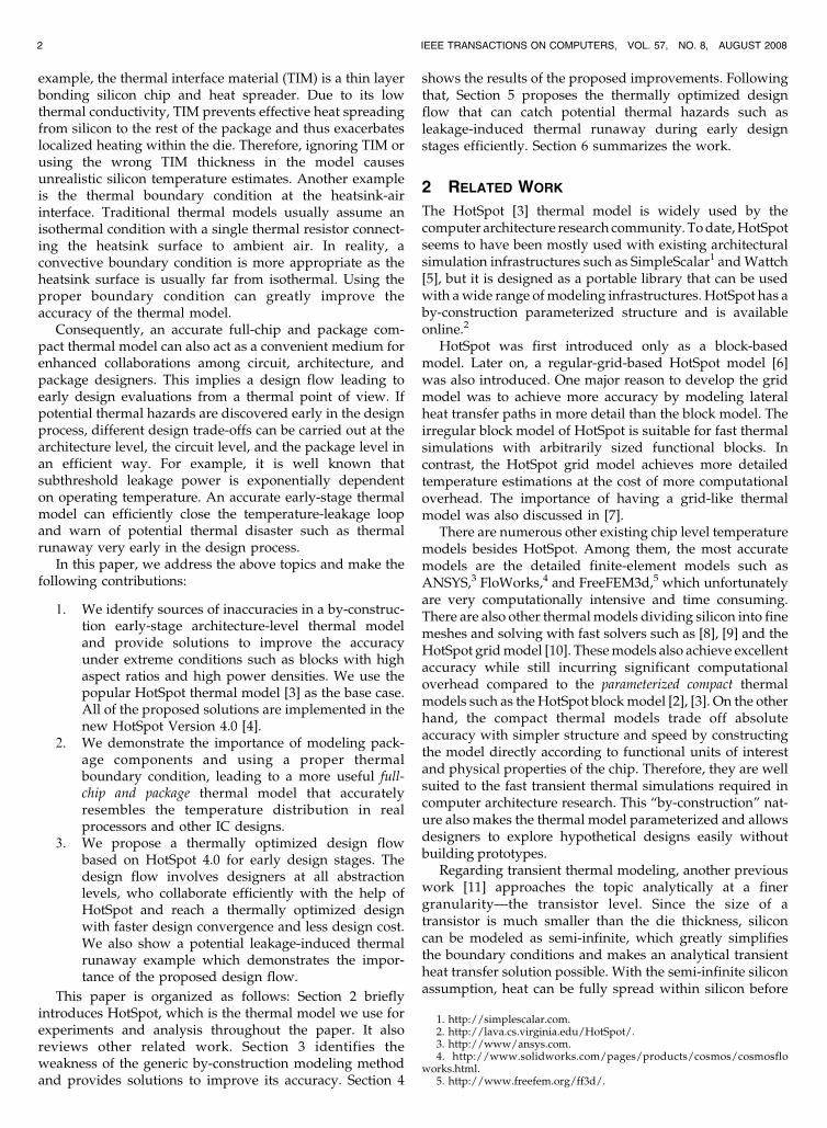
Figs. 7 and 8 show the comparisons among the HotSpot 3.1,HotSpot 4.0, ANSYS, and FreeFEM3d for different heatsource sizes. We also plot the HotSpot 3.1 results with unity-aspect-ratio (sub)blocks (HS3.1-AR) to isolate the effect ofeach individual aforementioned modifications (i.e., unityaspect ratio and nonisothermal boundary condition). As canbe seen, the HotSpot 4.0 block model is much more accuratethan the earlier HotSpot 3.1 block model.
For a smaller heat source size (1 mm to 5 mm), thesignificant error of HotSpot 3.1 is caused by the extremeaspect ratio (10:1) of the four long and narrow blocks thatare adjacent to the center small heat source block. InHotSpot 4.0, these long, narrow blocks are automatically
6 IEEE TRANSACTIONS ON COMPUTERS, VOL. 57, NO. 8, AUGUST 2008
Fig. 4. (a) EV6 block relative temperatures with good thermal interface
material. (b) EV6 block relative temperature errors with respect to
ANSYS, with good thermal interface materials ðkTIM ¼ 7:5W=ðm �KÞÞ.
Fig. 5. (a) EV6 block relative temperatures with worse thermal interface
materials. (b) EV6 block relative temperature errors with respect to
ANSYS with worse thermal interface materials ðkTIM ¼ 1:33W=ðm �KÞÞ.
Fig. 6. (a) Floorplan with a 1 mm center square heat source dissipating
1.66 W. Notice the neighboring high aspect ratio blocks. (b) The
neighboring high aspect ratio blocks are divided into square subblocks.
divided into 10 subblocks with aspect ratios of 1:1; thus theaccuracy is greatly improved (see the left part of the “HS3.1AR” curves for small heat source sizes).
For a larger heat source size (e.g., 19 mm, which has 600 Wof power), the significant error of HotSpot 3.1 is caused bythe fact that the upper surfaces of the heat spreader andthe heatsink are no longer close to being isothermal, soapproximating them with single nodes yields significanterrors. In HotSpot 4.0, the isothermal nodes are removed.Instead, we model the heatsink at the same level of detailas the silicon die and use a constant heat transfercoefficient ðh ¼ 2777:7 W=m2-KÞ for each subarea of theheatsink-ambient interface. This significantly improves theaccuracy for large-size heat sources (see the significantimprovement for larger heat source sizes from “HS3.1 AR”to “HS4.0”).
Here again, by eliminating the isothermal nodes inpackage and dividing high-aspect-ratio blocks into sub-blocks with unit aspect ratios, the HotSpot block modelgreatly improves its accuracy.
4.1.3 Pulse Response for Bpred Unit in EV6 Floorplan
To evaluate the transient accuracy improvement ofHotSpot 4.0, we performed an experiment with powerpulses of different time scales.
In Fig. 9, power pulses of 100 �s, 1 ms, and 10 ms aresequentially applied to the Branch Predictor (Bpred) blockin the EV6 floorplan with a uniform power density of2 W=mm2 to verify HotSpot 4.0’s accuracy at different time
scales. Notice that the time axis is in log scale. We compareHotSpot 4.0 and HotSpot 3.1 results with ANSYS. As can beseen, HotSpot 4.0 significantly improves transient accuracyfor all time scales under this high-aspect-ratio and high-power-density extreme case.
We can see that, in addition to eliminating the isothermalnodes in the package and dividing high-aspect-ratio blocksinto subblocks with unit aspect ratios, the HotSpot blockmodel’s transient accuracy is also improved by using aconstant scaling factor of 0.5 to approximate the thermaltime constant of the distributive nature of transienttemperature evolvement. The scaling factor comes fromthe analogous electrical distributed RC circuit whose timeconstant is half of the one-ladder RC circuit [25].
Based on the above steady-state and transient experi-ments and comparisons among the HotSpot block model,ANSYS, and FreeFEM3d, we can see that the improvedHotSpot 4.0 model is accurate as a by-construction compactthermal model for architecture-level and other early-stagedesign levels. The small inaccuracies come from the factthat the compact thermal model trades off accuracy toachieve greater model compactness.
4.2 TIM’s Impact on Chip Temperature
Earlier in the paper, we mentioned that package compo-nents can greatly affect the temperature distribution acrossthe silicon die. In this section, we show some examplethermal analysis regarding one particular packaging com-ponent—TIM that bonds the silicon die to the heat spreader.
With the flexibility of the improved parameterizedcompact thermal model, we can easily investigate the thermalimpacts of different TIM properties such as its thickness, voidsize, and attaching surface roughness in the early designstages and provide important insights for computer archi-tects, circuit designers, and package designers.
We first show how the thickness of TIM affects silicon dietemperature distribution. Fig. 10 plots the across-dietemperature difference from the compact thermal modelwith different TIM thickness.
As can be observed in Fig. 10, thicker TIM results in poorheat spreading that leads to large temperature differencesacross the die. We can see that thick TIM can lead to verylarge die temperature difference across the die ð> 50�CÞ.
HUANG ET AL.: ACCURATE PRE-RTL TEMPERATURE-AWARE DESIGN USING A PARAMETERIZED, GEOMETRIC THERMAL MODEL 7
Fig. 7. Center temperature for different heat source sizes, with good
thermal interface material ðkTIM ¼ 7:5W=ðm �KÞÞ, power density is
1:66 W=mm2.
Fig. 8. Center temperature for different heat source sizes, with worse
thermal interface material ðkTIM ¼ 1:33W=ðm �KÞÞ, power density is
1:66 W=mm2.
Fig. 9. Transient temperature response for different power pulse-
widths applied to the branch predictor of EV6. Power density is
2W=mm2 ðkTIM ¼ 7:5W=ðm �KÞÞ.

Even with nominal TIM thickness, which is 20 �m for thisdesign, the temperature difference across the die is still24�C. This means that the bottom surface of the die cannotbe modeled as an isothermal surface. If the TIM is thickenough, the resulting extremely large temperature differ-ences across the die may be disastrous to circuit perfor-mance and die/package reliability. Using a better heatsinkwill only lower the average silicon temperature but will nothelp to reduce the temperature difference. This analysissuggests that using the thinnest possible TIM is one of thekey issues for package designers to consider. On the otherhand, with the known TIM thickness that can be bestassembled in a package with state-of-the-art packagingtechnology, it is the task of circuit designers and computerarchitects to design proper circuits and architectures tomaintain the temperature difference across die within amanageable level.
As another example, Fig. 11 shows the relationshipbetween the size of TIM void and the hot spot temperature.During the packaging process, it is almost unavoidable toleave voids or air bubbles in the TIM. In the compactthermal model, the void in TIM can be easily modeled byintroducing higher vertical TIM thermal resistance to thegrid cell where the void resides. Different sizes of the TIMvoid can be modeled by different sizes of the grid cell. Forthe simulations in Fig. 11, we put the TIM void right underthe hottest grid cell, thus modeling the highest possible dietemperature in the presence of a void with different sizes.
As can be seen in Fig. 11, if the hot spot temperature of thedesign is 95�C, a void or air bubble in the TIM with a size of0.25 mm2 can make the hot spot temperature drasticallyhigher (290�C), which inevitably leads to a thermal run-away of the chip. Therefore, it is desirable to improve thepackaging techniques to make the size of the TIM void assmall as possible. Package designers usually have theexpertise to know typical TIM void sizes for differentpackaging processes. They can include this information inthe thermal model. By doing this, the thermal model is nowable to provide the possible worst-case temperature regard-ing TIM void defects. The consequent architecture andcircuit design decisions can thus avoid potential thermalhazards caused by the TIM void defects.
Another important TIM property that affects the dietemperature is the surface roughness, i.e., nonuniform TIM.In a real-life chip packaging process, the bottom surface ofthe die and the TIM’s attaching surface cannot be perfectlysmooth. As shown in Fig. 12, TIM is only attached to the dieat the bumps of the TIM surface. This causes ineffective heatconduction and, hence, higher die temperature compared tothe case where TIM and the die attach to each otherperfectly. In order to investigate the impact of TIMnonuniformity to the die temperature, we change thethermal model of the TIM layer according to that inFig. 12, where we simply model the nonuniformity of theTIM surface as tiny bumps with spacing 2L. The size of eachgrid cell is set to L. Therefore, heat can only be conductedthrough the grid cells representing the touching bumps.Grid cells representing the valleys are essentially tiny voidsthat do not touch the die and have extremely low thermalconductivity. The value of L thus can be used as anindicator of the nonuniformity of the TIM surface—thesurface is rougher when L is larger and vice versa. Fig. 13 isthe model results showing the relationship between L
(nonuniformity) and die temperatures, where L ¼ 0 means
8 IEEE TRANSACTIONS ON COMPUTERS, VOL. 57, NO. 8, AUGUST 2008
Fig. 10. The impact of TIM thickness on silicon die temperature
difference [20].
Fig. 11. The impact of the size of the void defect in TIM on the silicon die
hottest temperature. Temperatures are normalized to the ideal case
where there is no void defect in the TIM layer. TIM void sizes are with
the unit of mm2 [20].
Fig. 12. Close-up view of the TIM/die attaching surface. Surface
nonuniformity is indicated by L [20].
Fig. 13. Hottest die temperature and average die temperature versus the
nonuniformity of the TIM attaching surface. The larger L is, the rougher
the attaching surface is. L is defined in Fig. 12 [20].
the TIM surface is perfectly uniform. As observed, even atiny nonuniform TIM surface (e.g., L ¼ 5�m) can signifi-cantly raise both the hottest and the average die tempera-ture (by about 10 degrees). Package designers again usuallyhave the specifications of the surface nonuniformities fordifferent packaging processes. Without considering suchpackage processing specifications, it is inevitable that athermal model underestimates the die temperature andleads to designs that are not thermally optimized anddesigns with a higher probability of premature failures.
4.3 Trade-Offs of Using Hotspot 4.0
While HotSpot 4.0 has better accuracy under more extremeconditions, it also introduces more computational overheadthan HotSpot 3.1 due to the increased number of nodes inboth silicon and package components. The overhead isusually negligible when the number of blocks is relativelysmall. HotSpot 4.0 is extremely useful when there are veryhigh-power density blocks with high aspect ratio (e.g.,BPred and IntReg with low-conductivity TIM in Fig. 5) orthe total power of the chip is extremely high (e.g., the right-end points in Figs. 7 and 8 corresponding to the 19 mm �19 mm 600 W heat source). However, if the floorplan hastens and hundreds of blocks, HotSpot 3.1 may be a bettertrade-off between computation complexity and accuracy.
5 A THERMALLY OPTIMIZED DESIGN FLOW
As temperature management is more challenging as theresult of the nonideal CMOS scaling, considering thermalissues early in the design process becomes imperative. Eventhough the recent trend toward many-core chips can, tosome extent, alleviate localized heating due to a moreuniform power distribution compared to traditional single-and dual-core designs, accurately modeling local tempera-ture variation using HotSpot is still important due to thefact that the high-activity cores are usually surrounded bycool local caches; hence, local temperature distribution maystill be far from uniform. In addition, wafer thickness alsoscales down, resulting in less efficient within-silicon heatspreading and possibly more prominent localized heating,not to mention multicore chips with heterogeneous coresthat can vary significantly in terms of power consumptionand temperature among different cores.
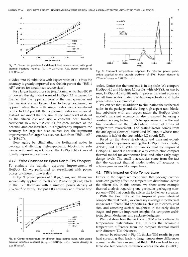
The HotSpot model is unique because it efficientlymodels both chip and package temperatures with satisfac-tory accuracy for any type of processor designs at any levelof detail. This is the key to more effective collaborationsamong computer architects, circuit designers, and packagedesigners. With the help of such an accurate full-chip andpackage compact thermal model, an early-stage thermallyoptimized design flow is proposed in this section toaccurately predict potential thermal hazards and to achieveeconomical designs with faster design convergence.
5.1 The Design Flow
Fig. 14 illustrates the proposed prelayout design flow. Asshown in Fig. 14, circuit designers first design basic blockssuch as macros and each macro has a simulated dynamicpower for a certain workload. It also has an estimatedlayout bounding box. Computer architects then assemble a
preliminary microarchitecture-level floorplan. At this point,
initial total power, including the rough estimation of
leakage power, can be used for a package designer to
propose a preliminary package design. All of the informa-
tion about power, floorplan, and package is used to
construct a compact thermal model that can perform
thermally self-consistent leakage power calculations, as
shown in the highlighted inner loop in Fig. 14. The resulting
temperature map can then be utilized to perform tempera-
ture-critical reliability analysis (e.g., interconnect electromi-
gration, gate-oxide breakdown, and package deformation)
and temperature-related performance analysis (e.g., inter-
connect and device delay and power grid IR drop).The results of all this analysis, together with the total
power, are then compared to the design goals. If the goals
are not satisfied, different trade-offs can be made—circuit
designers may need to invent novel circuits with lower
power dissipation, computer architects may have to think
more about new architectures and different floorplans to
better manage power and temperature, or package de-
signers may need to propose more advanced, usually more
expensive, packages. On the other hand, if the design goals
are fully satisfied, we still need to check whether the design
is too conservative and the design margin is too large for the
application. We can then improve the conservative design
by either introducing more aggressive circuit and/or
architecture solutions to enhance performance or using
simpler and cheaper packages to reduce the cost of the final
product. These decisions and trade-offs can then be
evaluated using the thermal analysis, again following the
HUANG ET AL.: ACCURATE PRE-RTL TEMPERATURE-AWARE DESIGN USING A PARAMETERIZED, GEOMETRIC THERMAL MODEL 9
Fig. 14. A design flow showing the compact thermal model acts as a
convenient medium for productive collaborations for designers at the
circuit, architecture, and package levels [20].
same flow until an optimal design point is reached. Then,one can proceed to the physical design stage.
With the above design flow, the potential thermalhazards can be discovered and dealt with early andefficiently; thus, the design is optimized from a thermalpoint of view.
5.2 An SoC Design Example
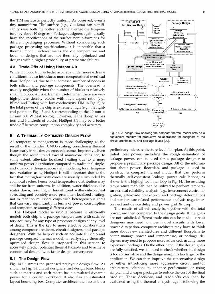
To illustrate the importance of adopting such a thermallyoptimized design flow early in the design process, we showthe thermal analysis together with the temperature-leakageloop for an SoC design. We use InCyte1, a novelcommercialized early design estimation tool,7 to reconstructan SoC design based on the published 180 nm design datain [27]. This SoC design does not have an integratedheatsink due to its low power consumption. It uses naturalconvection from a metal covering lid, which acts as the heatspreader, as the cooling method.
We use HotSpot 4.0 for the thermally self-consistentleakage analysis of this SoC design. Because a heatsink isnot present in the package, we apply the natural convectionboundary condition at the surface of the thin lid that isattached to the silicon substrate. Notice that, without theimprovement of directly modeling the convection boundarycondition in HotSpot 4.0, it is impossible to accuratelysimulate such a scenario because, under natural convection,the package surface is obviously not isothermal.
We pick logic and memory modules similar to those in[27] from InCyte’s incorporated IP libraries and come upwith an early SoC design whose total power is almostidentical to data reported in [27]. InCyte also outputs apreliminary floorplan for the design. Although the area ofeach block is also similar to the original design, the relativelocations of different blocks are noticeably different. This isacceptable since InCyte is a tool for early stage design. Inaddition, notice that InCyte estimates leakage power of eachblock at a constant temperature. Following that, we useHotSpot to estimate chip temperature distribution and picka proper package from InCyte’s package library for thisdesign based on data estimated from InCyte. If we assumethat the on-chip highest temperature constraint is 85�C andthe ambient temperature is 25�C, we find that the thermalpackage needs to have a lumped thermal resistance of18.2 K/W, which is common for standard SBGA packages,in order to keep the hot spot temperature below 85�C. Theestimated temperature map of this 180 nm design is shownin Fig. 15.
Because InCyte does not yet include the temperaturedependency of leakage, whereas subthreshold leakage isexponentially dependent on temperature, we double-checkto see whether the thermally self-consistent leakage powercauses thermal problems to this 180 nm SoC design. UsingHotSpot and the simplistic leakage model in [20] to iteratethe temperature-leakage loop, as shown in Fig. 14, afterconvergence, we find that the final total leakage is only anegligible 546 �W for this design with the picked package.Therefore, the above temperature estimation is quiteaccurate without considering the temperature-leakage loop.
However, if we redesign this SoC design in a 90 nmtechnology, there are two design possibilities: 1) We scaleboth the area and active power of each individual blocksand thus maintain the same function and complexity. Thismeans that the total power of the entire design is also scaledaccordingly; thus, the power density remains the same dueto area scaling. Therefore, we can use a cheaper thermalpackage for less overall power consumption and keep thechip below the 85�C thermal constraint. 2) Since ITRS [1]projects that the die size and power remain the same, if notincreasing, across different technology nodes, we canalternatively assume the total active power and chip arearemain the same as those in the 180 nm design. Assuming afloorplan similar to that in 180 nm technology, this isequivalent to adding more parallelism (such as moreprocessing cores and higher memory bandwidth) to thedie and designing the chip for higher throughput byburning more power. In this case, with the same18.2 K/W thermal package, after iterating the leakage-temperature loop, the hottest on-chip temperature exceedsthe thermal threshold and eventually causes thermal run-away. The reason is twofold: 1) At 90 nm, a greater fractionof total power consumption is caused by leakage [1], and2) the subthreshold leakage power’s dependency ontemperature is stronger at 90 nm than at 180 nm (see theleakage model coefficients shown in [28], [29]). The resultsare listed in Table 1.
The above SoC design example shows that it is crucial toincorporate thermal estimations (such as leakage-tempera-ture dependence) early in the design process in order tolocate potential thermal hazards that are too costly to fix inthe later design stages. At this early design stage, possiblesolutions to the SoC design at 90 nm can be 1) circuitdesigners can choose IPs that have high-Vt transistors anduse reverse body-bias or sleep transistors for noncriticalpaths to reduce leakage, 2) architects can consider usingdynamic voltage and frequency scaling (DVFS), migratingcomputation [3], [28], more parallelism, and temperature-aware floorplanning techniques [30], etc. to reduce hot spottemperatures, and, alternatively, 3) package designers needto consider the possibility of adding a heatsink or a fan.Trade-offs among portability, cost, performance, andtemperature have to be made in this case by following the
10 IEEE TRANSACTIONS ON COMPUTERS, VOL. 57, NO. 8, AUGUST 2008
7. http://www.chipestimate.com/.
Fig. 15. Estimated temperature map of an SoC design at 180 nm
technology, based on the data in [27] and InCyte. Temperatures are in �C.

design flow in Fig. 14. Unlike HotSpot 4.0, other existingthermal modeling approaches are either not accurateenough (e.g., neglecting package component details orusing the wrong boundary conditions) or too time-consum-ing (e.g., detailed FEM) and, hence, are not suitable for sucha design trade-off analysis early in the design process.
6 CONCLUSIONS
In this paper, we first present improvements to an efficientby-construction compact thermal model, like HotSpot, tomake it accurate even under scenarios such as high aspectratio blocks and high power density and to better modelrealistic convective boundary conditions for thermal pack-age components. The accuracy improvements of bothsteady-state and transient temperatures are confirmed bycomparing with finite-element models in ANSYS andFreeFEM3d. The importance of accurate considerationsand modeling of package components also determines theaccuracy of the die-level temperature estimations. Severalexamples are presented to illustrate the impact of TIM ondie temperature distribution. With the improvements of themodel structure and the proper inclusion of packagecomponents, thermal models such as HotSpot 4.0 canfurther act as a convenient communication medium formore efficient cooperations among computer architect,circuit designers, and package designers, thus achieving athermally optimized design early in the design stages. Theimportance of adopting such an early stage thermallyoptimized design flow is illustrated by the detection ofpotential thermal runaway in the early stage analysis for a90 nm SoC design.
ACKNOWLEDGMENTS
The authors would like to thank Pierre Michaud andDamien Fetis from IRISA/INRIA, France, for the interestingdiscussions and generous help on FreeFEM3d. They alsothank Jeff Ng, Nozar Nozarian, and Miles McGowan fromChipEstimate Inc. for their help with InCyte. This work isfunded by US National Science Foundation CRI Grant CNS-0551630 and has partial support from a MARCO IFC Grant.
REFERENCES
[1] The Int’l Technology Roadmap for Semiconductors (ITRS), 2003.[2] W. Huang, R. Stan, and K. Skadron, “Parameterized Physical
Compact Thermal Modeling,” IEEE Trans. Components and Packa-ging Technologies, vol. 28, no. 4, pp. 615-622, Dec. 2005.
[3] K. Skadron, K. Sankaranarayanan, S. Velusamy, D. Tarjan, M.R.Stan, and W. Huang, “Temperature-Aware Microarchitecture:Modeling and Implementation,” ACM Trans. Architecture and CodeOptimization, vol. 1, no. 1, pp. 94-125, Mar. 2004.
[4] W. Huang, K. Sankaranarayanan, R.J. Ribando, M.R. Stan, and K.Skadron, “An Improved HotSpot Block-Based Thermal Modelwith Granularity Considerations,” Proc. Workshop Duplicating,Deconstructing, and Debunking in conjunction with the Int’l Symp.Computer Architecture, June 2007.
[5] D. Brooks, V. Tiwari, and M. Martonosi, “Wattch: A Frameworkfor Architectural-Level Power Analysis and Optimizations,” Proc.Int’l Symp. Computer Architecture, pp. 83-94, June 2000.
[6] W. Huang, M.R. Stan, K. Skadron, K. Sankaranarayanan, and S.Ghosh, “Compact Thermal Modeling for Temperature-AwareDesign,” Proc. 41st Design Automation Conf., pp. 878-883, June 2004.
[7] P. Chaparro, J. Gonzalez, G. Magklis, Q. Cai, and A. Gonzalez,“Understanding the Thermal Implications of Multicore Architec-tures,” IEEE Trans. Parallel and Distributed Systems, vol. 18, no. 8,pp. 1055-1065, Aug. 2007.
[8] Y. Yang, Z.P. Gu, C. Zhu, R.P. Dick, and L. Shang, “ISAC:Integrated Space and Time Adaptive Chip-Package ThermalAnalysis,” IEEE Trans. Computer-Aided Design, vol. 26, no. 1,pp. 86-99, Jan. 2007.
[9] W. Wu, L. Jin, J. Yang, P. Liu, and S.X.-D. Tan, “Efficient PowerModeling and Software Thermal Sensing for Runtime Tempera-ture Monitoring,” ACM Trans. Design Automation of ElectronicSystems, vol. 12, no. 3, Aug. 2007.
[10] W. Huang, S. Ghosh, S. Velusamy, K. Sankaranarayanan, K.Skadron, and M.R. Stan, “HotSpot: A Compact Thermal ModelingMethodology for Early-Stage VLSI Design,” IEEE Trans. Very LargeScale Integration (VLSI) Systems, vol. 14, no. 5, pp. 501-513, May2006.
[11] N. Rinaldi, “On the Modeling of the Transient Thermal Behaviorof Semiconductor Devices,” IEEE Trans. Electronic Devices, vol. 48,no. 12, pp. 2796-2802, Dec. 2001.
[12] D. Fetis and P. Michaud, “An Evaluation of HotSpot-3.0 Block-Based Temperature Model,” Proc. Workshop Duplicating, Decon-structing, and Debunking in conjunction with Int’l Symp. ComputerArchitecture, June 2006.
[13] M.R. Stan, K. Skadron, M. Barcella, W. Huang, K. Sankaranar-ayanan, and S. Velusamy, “HotSpot: A Dynamic CompactThermal Model at the Processor-Architecture Level,” Microelec-tronics J., vol. 34, pp. 1153-1165, 2003.
[14] T.-Y. Wang and C.C.-P. Chen, “3-D Thermal-ADI: A Linear-TimeChip Level Transient Thermal Simulator,” IEEE Trans. Computer-Aided Design of Integrated Circuits and Systems, vol. 21, no. 12,pp. 1434-1445, Dec. 2002.
[15] H. Su, F. Liu, A. Devgan, E. Acar, and S. Nassif, “Full ChipEstimation Considering Power Supply and Temperature Varia-tions,” Proc. Int’l Symp. Low Power Elec. Design, pp. 78-83, Aug.2003.
[16] P. Li, L. Pileggi, M. Asheghi, and R. Chandra, “Efficient Full-ChipThermal Modeling and Analysis,” Proc. Int’l Conf. Computer-AidedDesign, 2004.
[17] C.J.M. Lasance, “Two Benchmarks to Facilitate the Study ofCompact Thermal Modeling Phenomena,” IEEE Trans. Componentsand Packaging Technologies, vol. 24, no. 4, pp. 559-565, Dec. 2001.
[18] M.-N. Sabry, “Compact Thermal Models for Electronic Systems,”IEEE Trans. Components and Packaging Technologies, vol. 26, no. 1,pp. 179-185, Mar. 2003.
[19] E.G.T. Bosch, “Thermal Compact Models: An AlternativeApproach,” IEEE Trans. Components and Packaging Technologies,vol. 26, no. 1, pp. 173-178, Mar. 2003.
[20] W. Huang, E. Humenay, K. Skadron, and M. Stan, “The Need for aFull-Chip and Package Thermal Model for Thermally OptimizedIC Designs,” Proc. Int’l Symp. Low Power Electronic Design, pp. 245-250, Aug. 2005.
HUANG ET AL.: ACCURATE PRE-RTL TEMPERATURE-AWARE DESIGN USING A PARAMETERIZED, GEOMETRIC THERMAL MODEL 11
TABLE 1As Technology Scales, Temperature Dependence of Subthreshold Leakage Power Becomes More Problematic
Without early-stage thermally optimized design flow (Fig. 14), thermal runaway can happen even for low-power SoC designs.

[21] K. Banerjee, S.C. Lin, A. Keshavarzi, and V. De, “A Self-ConsistentJunction Temperature Estimation Methodology for NanometerScale ICs with Implications for Performance and ThermalManagement,” Proc. Int’l Electron Devices Meeting, pp. 3671-3674,2003.
[22] L. He, W. Liao, and M.R. Stan, “System Level Leakage ReductionConsidering the Interdependence of Temperature and Leakage,”Proc. 41st Design Automation Conf., pp. 12-17, June 2004.
[23] P. Chaparro, J. Gonzalez, and A. Gonzalez, “Thermal-EffectiveClustered Microarchitecture,” Proc. First Workshop Temperature-Aware Computer Systems, June 2004.
[24] E.C. Samson, S.V. Machiroutu, J.-Y. Chang, I. Santos, J. Hermerd-ing, A. Dani, R. Prasher, and D.W. Song, “Interface MaterialSelection and a Thermal Management Technique in Second-Generation Platforms Built on Intel Centrino Mobile Technology,”Intel Technology J., vol. 9, no. 1, Feb. 2005.
[25] H.B. Bakoglu, Circuits, Interconnections, and Packaging for VLSI.Addison-Wesley, 1990.
[26] Y. Zhang, D. Parikh, K. Sankaranarayanan, K. Skadron, and M.Stan, “HotLeakage: A Temperature-Aware Model of Subthresholdand Gate Leakage for Architects,” Technical Report CS-2003-05,Computer Science Dept., Univ. of Virginia, 2003.
[27] H. Stolberg, S. Moch, L. Friebe, A. Dehnhardt, M. Kulaczewski, M.Berekovic, and P. Pirsch, “An SoC with Two Multimedia DSPsand a RISC Core for Video Compression Applications,” Digest ofPapers, IEEE Int’l Solid-State Circuits Conf., Feb. 2004.
[28] S. Heo, K. Barr, and K. Asanovic, “Reducing Power Densitythrough Activity Migration,” Proc. Int’l Symp. Low Power Electro-nics and Design, pp. 217-222, Aug. 2003.
[29] J. Srinivasan, S.V. Adve, P. Bose, and J.A. Rivers, “The Impact ofTechnology Scaling on Lifetime Reliability,” Proc. Int’l Conf.Dependable Systems and Networks, June 2004.
[30] K. Sankaranarayanan, S. Velusamy, M.R. Stan, and K. Skadron, “ACase for Thermal-Aware Floorplanning at the MicroarchitecturalLevel,” The J. Instruction-Level Parallelism, vol. 7, Oct. 2005.
Wei Huang received the BE degree in elec-trical engineering from the University ofScience and Technology of China and thePhD degree in electrical engineering from theUniversity of Virginia. He is currently with theComputer Science Department at the Univer-sity of Virginia as a postdoctoral researcher.His research interests include VLSI circuits andcomputer architecture with considerations onthermal, power, variability, and reliability is-
sues. He is a member of the IEEE.
Karthik Sankaranarayanan received the BEdegree in computer science and engineeringfrom Anna University, Chennai, India, in 2000and the MS degree from the University ofVirginia, Charlottesville, in 2003. He is currentlyworking toward the PhD degree at the Universityof Virginia. He is a member of the LAVALaboratory at the University of Virginia. Hisresearch interests include computer architecturein general and thermal and power-aware micro-
architectures in particular.
Kevin Skadron received the BS and BAdegrees in electrical and computer engineeringand economics from Rice University and thePhD degree in computer science from PrincetonUniversity. He is the cofounder and the associ-ate editor-in-chief of the IEEE Computer Archi-tecture Letters. He is an associate professor inthe Department of Computer Science at theUniversity of Virginia. His research interestsfocus on physical design challenges and pro-
gramming models for multicore/manycore architectures, includinggraphics architectures. He is a member of the Eta Kappa Nu andOmicron Delta Epsilon and he is a senior member of the ACM, the IEEE,the IEEE Computer Society, and the IEEE Circuits and SystemsSociety.
Robert J. Ribando received all of his degreesfrom Cornell University. He is an associateprofessor in the Department of Mechanical andAerospace Engineering at the University ofVirginia. Prior to coming to Virginia, he was onthe research staff of the Advanced ReactorsSafety Section at Oak Ridge National Labora-tory. His research and teaching interests includecomputational fluid dynamics and heat transferand the graphical display of quantitative informa-
tion. The applications have included nuclear reactor heat transfer,strongly rotating flows, biomedical flows, turbomachinery flows, etc.From 1992 to 1995, he held the Lucien Carr III Chair in EngineeringEducation, a temporary position intended to recognize and encouragethe use of technology in instruction. He is currently writing a textbookand CD applying modern computational methods and visualization to thestudy of heat transfer.
Mircea R. Stan received the diploma in electro-nics and communications from “Politehnica”University in Bucharest, Romania, in 1984 andthe MS and PhD degrees in electrical andcomputer engineering from the University ofMassachusetts, Amherst, in 1994 and 1996.Since 1996, he has been with the Department ofElectrical and Computer Engineering at theUniversity of Virginia, where he is currently anassociate professor. He is teaching and doing
research on high-performance low-power VLSI, temperature-awarecircuits and architecture, embedded systems, and nanoelectronics. Hehas more than eight years of industrial experience, has been a visitingfaculty member at the University of California, Berkeley, in 2004-2005,IBM in 2000, and Intel in 2002 and 1999. He received the NSF CAREERaward in 1997 and was a coauthor of the papers which received the bestpaper awards at GLSVLSI 2006, ISCA 2003, and SHAMAN 2002. He isthe chair of the VLSI Systems and Applications Technical Committee(VSA-TC) of IEEE CAS, general chair for ISLPED 2006 and forGLSVLSI 2004, technical program chair for NanoNets 2007 and ISLPED2005, and a member of the technical committees of numerousconferences. Since 2004, he has been an associate editor for the IEEETransactions on Circuits and Systems Systems I and, from 2001 to2003, an associate editor for the IEEE Transactions on VLSI Systems.He ws also a guest editor for the Computer special issue on power-aware computing in December 2003 and a distinguished lecturer for theIEEE Solid-State Circuits Society (SSCS) in 2007-2008 and the IEEECircuits and Systems (CAS) Society in 2004-2005. He is a seniormember of the IEEE and a member of the ACM, the IET (former IEE),and also of Eta Kappa Nu, Phi Kappa Phi, and Sigma Xi.
. For more information on this or any other computing topic,please visit our Digital Library at www.computer.org/publications/dlib.
12 IEEE TRANSACTIONS ON COMPUTERS, VOL. 57, NO. 8, AUGUST 2008
![ON THE PARAMETERIZED COMPLEXITY OF APPROXIMATE …matematicas.uis.edu.co/.../files/p-approx-counting.pdf · 1.1. Parameterized Complexity. Parameterized complexity theory [5], [3]](https://img.dokumen.tips/doc/110x75/5fa9b6c0f3b3624d395da859/on-the-parameterized-complexity-of-approximate-11-parameterized-complexity-parameterized.jpg)