Embed Size (px)
Citation preview

IEEE SENSORS JOURNAL, VOL. 5, NO. 4, AUGUST 2005 641
Electrostatically Actuated Resonant MicrocantileverBeam in CMOS Technology for the Detection
of Chemical WeaponsIoana Voiculescu, Mona E. Zaghloul, Fellow, IEEE, R. Andrew McGill, Eric J. Houser, and Gary K. Fedder
Abstract—The design, fabrication, and testing of a resonantcantilever beam in complementary metal–oxide semiconductor(CMOS) technology is presented in this paper. The resonantcantilever beam is a gas-sensing device capable of monitoringhazardous vapors and gases at trace concentrations. The new de-sign of the cantilever beam described here includes interdigitatedfingers for electrostatic actuation and a piezoresistive Wheatstonebridge design to read out the deflection signal. The reference resis-tors of the Wheatstone bridge are fabricated on auxiliary beamsthat are immediately adjacent to the actuated device. The wholedevice is fabricated using a 0.6- m, three-metal, double-polyCMOS process, combined with subsequent micromachining steps.A custom polymer layer is applied to the surface of the microcan-tilever beam to enhance its sorptivity to a chemical nerve agent.Exposing the sensor with the nerve agent simulant dimethyl-methylphosphonate (DMMP), provided a demonstrated detectionat a concentration of 20 ppb or 0.1 mg/m3. These initial promisingresults were attained with a relatively simple design, fabricatedin standard CMOS, which could offer an inexpensive option formass production of a miniature chemical detector, which containson chip electronics integrated to the cantilever beam.
Index Terms—Cantilever beam, complementary metal–oxidesemiconductor (CMOS) technology, electrostatic actuation, gassensor, nerve agent.
I. INTRODUCTION
I N order to allow widespread monitoring capacity, an inex-pensive and small sensing approach to detection is needed.
Using a micromachined sensor or system is a possible solutionto this need and provided the motivation for this work.
There is an acute need for highly sensitive, accurate, and rapiddetection techniques for chemical agents, toxic industrial chem-icals, and explosives. The onset of clinical responses after expo-
Manuscript received February 14, 2004; revised November 7, 2004. Thiswork was supported in part by the Transportation Security Administration(TSA), in part by the Bureau of Alcohol, Tobacco, Firearms, and Explosives(ATF), and in part by the Office of Naval Research (ONR). The associate editorcoordinating the review of this paper and approving it for publication was Dr.Arthur Sedlacek.
I. Voiculescu is with the Department of Mechanical and Aerospace Engi-neering, The George Washington University, Washington, DC 20052 USA(e-mail: [email protected]).
M. E. Zaghloul is with the Department of Electrical and Computer Engi-neering, The George Washington University, Washington, DC 20052 USA(e-mail: [email protected]).
R. A. McGill and E. J. Houser are with the Naval Research Laboratory, Wash-ington, DC 20375 USA (e-mail: [email protected]; [email protected]).
G. K. Fedder is with the Department of Electrical and Computer Engi-neering, Carnegie Mellon University, Pittsburgh, PA 15213-3890 USA (e-mail:[email protected]).
Digital Object Identifier 10.1109/JSEN.2005.851016
sure to hazardous chemicals is often rapid, so it is desirable tohave a large number of detectors covering wide geographicalareas, or for the individual to wear the detector as an unobtru-sive pager like device. For cost and size issues, it is attractiveto consider the use of micromachined technologies which offerthe capability for on chip electronics to lower costs and providehigh production yields.
A chemical sensor is a device, which converts chemical infor-mation into an analytically useful signal [1]. Chemical sensorsare important for a variety of industrial and environmental appli-cations, including the detection of hazardous chemicals, qualitycontrol in the food, perfume, and beverage industries, and med-ical applications [2].
A typical configuration for a chemical sensor includes asorbent layer deposited on an active area of a transducer [3].The interaction of a gas and the sorptive layer is monitored asa function of a physical change in the coating, and transducedinto an electrical signal for ease of recording or display. Foractive gas sampling, pneumatic connections and a gas pump arenormally required to make air flow over the chemical sensor.Conventional chemical sensors utilize transducers which arerelatively large and have millimeter sized dimensions [4]. Theadvent and maturation of microelectromechanical systems(MEMS) technology now offers many opportunities to dramati-cally reduce the size, cost, and power consumption of chemicalsensors [5]–[10]. Current state-of-the-art chemical detectorsare typically hand held systems.
II. SENSOR TECHNOLOGY AND DESCRIPTION
A. Principles of the Microcantilever Beam Gas Sensor
A cantilever beam chemical sensor consists of two key com-ponents: a gas sorptive layer, such as a polymer, and the can-tilever beam transducer. Two modes of operation of the can-tilever beam can be distinguished [10]. In the static mode, thebending of the cantilever beam upon mass loading and relatedsurface stress is measured. In the dynamic mode, the cantileverbeam can be actuated at its fundamental resonant frequency. Thefundamental resonant frequency in turn depends on the massloading of the cantilever beam.
The beam structures fabricated in this work were designedwith a range dimensions to explore the effect of device shape onresonant frequency, and mass sensitivity. Six different designswere included in a single chip. Short, wide, and thick cantileverbeams are preferred for higher resonant frequencies, and largesurface structures which maximize the area for polymer coatingand subsequent gas sorption. In this regard, the length ( ) and
1530-437X/$20.00 © 2005 IEEE

642 IEEE SENSORS JOURNAL, VOL. 5, NO. 4, AUGUST 2005
Fig. 1. Basic beam dimensions L andW.
the width ( ) of the cantilever beam are varied in order to de-termine the optimal dimensions for these structures; see Fig. 1.
is varied between 130 and 300 m, and is varied from 60to 150 m.
A thin layer of sorptive polymer is coated on the beam platesurface. This results in a frequency shift of the device to a newsignal baseline. In the absence of actual polymer thickness mea-surements, it is typical to quote the amount of polymer coated asa frequency shift. The uptake of different gases is monitored asan additional shift in the device frequency, which is reversible ifthe gas-polymer chemical interactions are reversible. The can-tilever beam gas sensor acts as a resonating microbalance, withmass increases normally leading to a decrease in the cantileverbeam resonant frequency.
The amount of gas mass sorbed to the cantilever beam can bedetermined from the frequency shift of the cantilever beam, andif a calibration curve has been developed, the concentration ofthe gas in the air can be computed.
The natural frequency of a simple undamped rectangular can-tilever beam is defined as [11]
(1)
where , , , and are the Young’s modulus, the moment ofinertia about the neutral axis, the mass per unit length, and thelength of the cantilever beam, respectively.
The natural frequency for the free undamped vibration of acomposite cantilever beam can be expressed by replacing thebending stiffness ( ) and mass per unit length ( ) terms from(1) with composite bending stiffness and composite mass perunit length. The resonant frequency for a composite cantileverbeam is given by (2)
(2)
where is the number of layers of the composite cantileverbeam, , , and are the effective Young’s modulus, themoment of inertia and the mass per unit length, of each layer,respectively [12]–[15].
For a microcantilever beam, and a uniformly deposited mass,the gravimetric change can be estimated with (3) [16]
(3)
where and are the resonant frequencies of the cantileverbeam after and before absorption and is the spring constant.
Fig. 2. Cantilever beam gas sensor. Electrodes are used for electrostaticactuation of the beam.
The spring constant for a composite cantilever beam with auniform cross section is given by [13]
(4)
and denoting the effective Young’s modulus and the mo-ment of inertia of the individual layers of the beam, respectively.The amount of gas sorbed in the polymer depends on the specificgas-polymer interaction(s), the amount of polymer, and the gasconcentration in the environment [3]. At a molecular level, thegas diffuses in and out of the polymer film, and the concentrationin the polymer rises until a dynamic equilibrium is reached. Forgases that are strongly bound to the polymer, desorption can befacilitated by the operation of a heater. In a cantilever beam’s.array format with each beam coated with a different polymer,the pattern of responses or fingerprint that results from a gas ex-posure can be used to identify the gas.
A diagram of the cantilever beam, which is employed in thiswork, is shown in Fig. 2. Electrostatic actuation is used to drivethe cantilever beam in a resonant mode. The resonant frequencyis measured by a set of piezoresistors connected in a Wheatstonebridge configuration. Only the beam tip is coated with the thinlayer of sorbent polymer.
B. Design and Fabrication of Complementary Metal–OxideSemiconductor (CMOS) Cantilever Beam Gas Sensor Chip
CMOS technology is the most common fabrication tech-nology for integrated circuits. Its combination with post-processmicromachining allows for integration of sensors and circuitryon the same chip. Micro structures integrated with CMOS arecommonly made from multilayers of silicon oxide, siliconnitride, polysilicon, and aluminum thin films.
The chip was designed in the Carnegie Mellon University(CMU) CMOS-MEMS technology using MEMSCAP-Xplorersoftware installed under Cadence. Typical die size for thisprocess is 2.5 2.5 mm. The foundry used in this work isbased on the Austrian Microsystems (AMS) process (0.6 m,three-metal, double-poly CMOS). The standard CMOS-MEMSprocess is followed by two maskless dry etch steps to release themicrostructures that are protected by the top-most metal layer.The RIE postprocessing steps were performed at CMU [17]. Inthe chip layout, suitable gaps are included to permit the RIEpost processing steps. An anisotropic reactive ion etch (RIE)with CHF and O is first used to remove the silicon oxidenot covered by any of the aluminum metal layers. This stepis followed by an isotropic RIE process using SF and O toremove the underlying silicon, and release the microstructure.

VOICULESCU et al.: ELECTROSTATICALLY ACTUATED RESONANT MICROCANTILEVER BEAM 643
Fig. 3. SEM image of beam 6. The resistors, which are part of the Wheatstonebridge, are marked to correspond to Fig. 4.
The key to the CMU CMOS-MEMS process is in the use ofmetallization as an etch-resistant mask to define the microstruc-tures. The CMU CMOS-MEMS process has been described pre-viously in detail [18].
The microstructural layers can be designed with any of thethree metal layers as the etch mask, with their thickness beinga function of the number of metal masking layers. In most sur-face micro-machined technologies, the design control is limitedto two planar dimensions of a mechanical structure. An advan-tage of the CMU CMOS technology is based on the availabilityof up to three metal layers, which offers the design flexibilityin a third dimension. Using different combinations of the threemetal layers, different beam thicknesses can be fabricated. Inthis work, the metal layer combinations of M1 and M3 wereused to generate devices with a thickness of 4.2 m [19].
The post-processed structures fabricated using CMUCMOS-MEMS technology with the AMS CMOS processhave the drawback that they typically exhibit bending afterrelease. The CMOS metal and dielectric layers, which formthe laminated structures, have different coefficients of thermalexpansion, which result in the bending of the released struc-tures [20]. However, the cantilever beam is electrostaticallyactuated perpendicular to the bending of the beam structures,so the device bending is not a negative design issue for thisapplication.
Six different designs of chemical sensors were included ina single test chip. An example cantilever beam, number 6, isshown in Fig. 3.
The cantilever beam is driven electrostatically, using the twosets of interdigitated fingers seen in Fig. 3. The fingers designedon the chip substrate, which are flat, are wired to the groundpad. The fingers, designed on opposite sides of the cantileverbeam are tilted out of the device plane and are wired togetherto a single bond pad, which is connected to an ac drive voltagesuperimposed on a dc voltage.
C. Design and Implementation of On-Chip Wheatstone Bridge
The resonant frequency is monitored with a highly symmet-rical on-chip Wheatstone bridge arrangement. Each device onthe fabricated chip includes a Wheatstone bridge arrangement.
Fig. 4. On-chip Wheatstone bridge arrangement (compare with Fig. 3).
The Wheatstone bridge transduces any change in resistancedue to the strain experienced by the piezoresistors, which can bemanifested by deflection or oscillation [21]. Using the Wheat-stone bridge configuration, the relative change in the resistanceof the piezoresistor is provided as an output voltage signal.Figs. 3 and 4 show the circuit and associated components ofthe device.
The full Wheatstone bridge has two piezoresistors andpositioned on the active cantilever beam, and two reference
resistors and which are situated on neighboring short,auxiliary beams, as shown in Fig. 3.
Two resistors connected in series are provided for each ref-erence resistor and positioned in the common-centroid arrange-ment to allow for improved resistance matching.
This particular Wheatstone bridge design used in this workpositions all of the resistors on beams, so that on release, eachresistor experiences the same changes in stress, and results ina similar degree of bending; see Fig. 3. This design allows theresistors to maintain their matched values before and after re-lease. For the electrical characterization of the cantilever beamgas sensors, the applied voltage at the input of the Wheatstonebridge was set at 6 V. The offset voltage of the Wheatstonebridge, when the cantilever beam was not actuated was between2 – 20 mV, depending on the cantilever beam design.
The resistance measurements were performed with a Summit11 651–6 Thermal Probe Station, with a Keithley 2400 sourcemeter, using Cascade Microtech DCP 150R Precision DCprobes.
III. SIMULATION AND MEASURMENT OF THE CANTILEVER
BEAM RESONANT FREQUENCIES
A. Finite-Element Simulation of the Cantilever BeamsResonant Frequencies
It is important to identify the true resonant mode of the can-tilever beams for any experimental measurements. The resolu-tion of the experimental measurements will be poor if the reso-nant frequencies are not known. Without this knowledge, a largebandwidth would be required, and resolution sacrificed. If ap-proximate resonant frequencies are known, the measurementscan be carried out with a smaller bandwidth around the esti-mated resonant frequency. Based on these considerations, a fi-nite-element analysis using ANSYS (version 6.1) was employedto model the first four resonant frequency modes of all the sixcantilever beams designed on the test chip [22].
The simulations were performed without a sorbent polymercoating. The cantilever beam is a multilayer structure fabricatedfrom silicon oxide, silicon nitride, polysilicon, and aluminumthin films. In order to perform the modal simulation withANSYS, the cantilever beam was modeled as a composite

644 IEEE SENSORS JOURNAL, VOL. 5, NO. 4, AUGUST 2005
Fig. 5. ANSYS simulation of the cantilever beam 1 resonant frequency. Onlythe first four modes are represented. The beam dimensions are; beam length55 �m, beam width 30 �m, plate length 70 �m, width 60 �m, and thickness4.2 �m.
TABLE IRESONANT FREQUENCY OF ALL THE BEAMS, SIMULATED
WITH ANSYS AND EXPERIMENTALLY DETECTED
beam. The mesh elements of all analyzed cantilever beamswere made using tetrahedral elements (SOLID 92).
The material properties of the different thin-film composite,such as Young’s modulus and density, were taken as previouslyreported [13]. Squeeze-film damping was not included in thesimulation because the beam structures are significantly bent,which reduces effects from air damping.
For cantilever beam 6, the ANSYS simulation of the reso-nant frequency is shown in Fig. 5, with the four lowest reso-nant modes. The corresponding cantilever beam SEM image isshown in Fig. 3. The resonant frequencies from the ANSYS sim-ulations of the six cantilever beams fabricated on the chip areprovided in Table I.
B. Electrostatic Actuation of the Cantilever Beam
The cantilever beam is excited electrostatically by applyinga dc voltage, which results in attractive Coulombic forces be-tween the interdigitated fingers. The cantilever beams are setinto oscillatory motion in a plane perpendicular to the beam.This is made possible in part due to the CMU CMOS-MEMSapproach, which results in bent structures.
The cantilever beam bending was analyzed with a WykoNT3300 white light interferometer at CMU. With no appliedvoltage on the cantilever beam, the bending for cantilever beam6 is shown in Fig. 6.
Fig. 6. Interferometer image of the cantilever beam 6. Applied voltage 0 V.The bending of the structure is noted at 7.63 �m.
Fig. 7. Interferometer image of the beam 6. DC 23 V was applied on theinterdigitated fingers. The bending of the structure is noted at 7.1 �m.
With a dc voltage of 23 V applied to the fingers of cantileverbeam 6, the device is shown to deflect toward the support by0.53 m, which is large enough for the electrostatic actuationof the cantilever beam. The deflection results are illustrated inthe interferometer image shown in Fig. 7.
The dc polarization voltage is applied between the electrodesfingers to create a surface charge and an ac voltage is superim-posed to drive the device with a harmonic force. The dc voltageapplied from an Agilent E3631A power supply to deflect thecantilever beams was 20 V, and an ac voltage of 4 Vp-p from aHewlett Packard HP 3588A spectrum analyzer was required todrive the oscillation of the beam.
Two piezoresistors which are part of the Wheatstone bridgeare integrated on each beam to monitor the cantilever beam de-flections. The output signal from the Wheatstone bridge, whichis not amplified, is applied at the input of the spectrum ana-lyzer in order to determine the resonant frequency. At the reso-nant frequency, the Wheatstone bridge output signal was mea-sured between 80 and 120 mV, depending on the dimensions ofeach cantilever beam, with the Wheatstone bridge biased at 6 V.The circuitry used to oscillate the cantilever beam is shown inFig. 8. A simple voltage divider is constructed to superimposethe varying ac voltage on the constant dc voltage.
The resonant frequency simulations with ANSYS were usefulto narrow the frequency range monitored by the spectrum an-alyzer. The resonant frequencies simulated with ANSYS and
VOICULESCU et al.: ELECTROSTATICALLY ACTUATED RESONANT MICROCANTILEVER BEAM 645
Fig. 8. Schematic of the circuitry used to drive the resonant beam gas sensor.
Fig. 9. Polymer drop is deposited close to the beam tip. The device bendingresults in an image that is out of focus.
measured with the circuitry are in good agreement and areshown in Table I. The differences maybe in part explained bythe absence of a complete simulation that would include thefingers and etch release holes.
IV. POLYMER AS ANALYTE SORPTIVE LAYER
The polymer used in this work is a functionalized polycar-bosilane, HCSA2. This polymer has been previously described[23], [24] and is a rubbery material with full flowing propertiesat room temperature. The beam’s resonant frequency shift re-sponse resulting from analyte sorption increases with increasingthickness of the polymer layer. At equilibrium, the thicker thepolymer layer will sorb more gas molecules, with a larger masschange to detect. There are limits to which the device can bepractically coated with a polymer film, that relate to the degra-dation of the cantilever beam quality or factor, and slowerkinetics with thicker polymer films. The lower values are re-lated to an increase in signal noise, which degrades the resolu-tion of the sensor.
The cantilever beam was coated with a dilute solution ofpolymer HCAS2 in Chloroform (0.03% w/w) with a piezoinkjet dispensing head. The dispensed drop is directed at thedesired location on the beam plate by viewing the cantileverbeam through a microscope during the coating process. It isimportant to avoid depositing excessive amounts of polymeron the interdigitated fingers which would prevent oscillation,see Fig. 9. Targeting the drop closer to the cantilever beam tipimproves the value.
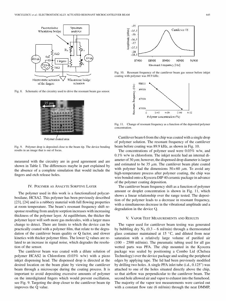
Fig. 10. Resonant frequency of the cantilever beam gas sensor before inkjetcoating with polymer was 89.9 kHz.
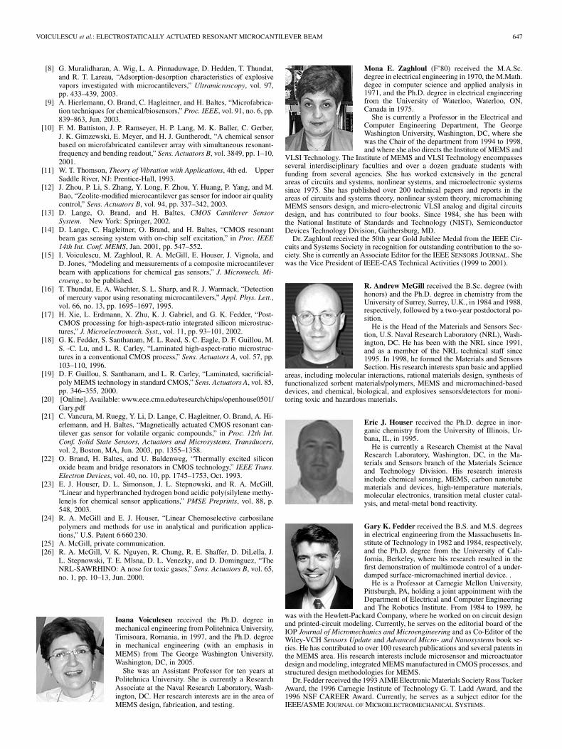
Fig. 11. Change of resonant frequency as a function of the deposited polymerconcentration.
Cantilever beam 6 from the chip was coated with a single dropof polymer solution. The resonant frequency of the cantileverbeam before coating was 89.9 kHz, as shown in Fig. 10.
The concentrations of polymer used were 0.03% w/w, and0.1% w/w in chloroform. The inkjet nozzle had an internal di-ameter of 30 m; however, the dispensed drop diameter is largerand estimated to be 35 m. The cantilever beam plate coatedwith polymer had the dimensions 50 60 m. To avoid anyhigh-temperature process after polymer coating, the chip waswire bonded onto a Kyocera DIP 40 ceramic package in advanceof the polymer coating deposition.
The cantilever beam frequency shift as a function of polymeramount or droplet concentration is shown in Fig. 11, whichshows a linear relationship over the range tested. The deposi-tion of the polymer leads to a decrease in resonant frequency,with a simultaneous decrease in the vibrational amplitude and adegradation in the device .
V. VAPOR TEST MEASUREMENTS AND RESULTS
The vapor used for cantilever beam testing was generatedby bubbling dry N (0.3 – 6 ml/min) through a thermostattedglass container maintained at 15 C, and diluted from nearsaturation with a relatively large volume of purified air(100 – 2500 ml/min). The pneumatic tubing used for all gaswetted parts was PFA. The chip mounted in the Kyocerapackage was sealed by positioning a Combo Lid (ChelseaTechnology) over the device package and sealing the peripheraledges by applying tape. The lid had been previously modifiedby drilling two holes. A single PFA inlet tube (i.d., 0.125”) wasattached to one of the holes situated directly above the chip,so that airflow was perpendicular to the cantilever beam. Thesecond hole allowed air and vapor to exhaust into the fumehood.The majority of the vapor test measurements were carried outwith a constant flow rate (6 ml/min) through the neat DMMP,

646 IEEE SENSORS JOURNAL, VOL. 5, NO. 4, AUGUST 2005
Fig. 12. Cantilever beam response upon exposure to various DMMPconcentrations. Frequency shifts are marked �f1 and �f2.
Fig. 13. Cantilever beam response upon exposure to DMMP concentrationsvarying from 43 to 0.1 mg=m . The detection limit is 0.1 mg=m .
and by carrying the diluent air from 100 to 2500 ml/min.Above 2500 ml/min, the noise of the beam became excessive.The airflow was delivered at a temperature of 20 C, with arelative humidity (RH) of 0%. The sealed chip manifold wasnot actively temperature controlled. In a typical experiment, thevapor on and off time periods were fixed at 5 min.
During vapor tests, the cantilever beam was operated as de-scribed earlier and the sensor response monitored as a shift in theresonant frequency. The frequency sweep, with a resolution of 5Hz, over the complete 3-kHz range was set at 5 s. The graphicalfrequency data, and the resonant frequency were displayed onthe spectrum analyzer. The cantilever beam selected for testingwas number 6. Initial tests were carried out by exposing a barecantilever beam to DMMP vapor at elevated concentrations.These experiments showed no measurable frequency shift. Thesame chip was then coated with a single drop of polymer solu-tion at two different concentrations (0.03% w/w, and 0.1% w/w,in chloroform). This device was then exposed to DMMP vaporat concentrations which were ramped from 43 to 0.1 mg m ina repeated fashion.
The polymer thickness was estimated from the known solu-tion concentration, the approximate drop volume, and the sur-face area covered. The computed mean thickness is 335 nm. Atthis thickness, the sensor time constant to 90% of signal wasapproximately 10 s. Example frequency sweeps taken from thespectrum analyzer are shown in Fig. 12. The cantilever beamsensor response as a function of DMMP concentration is shownin Figs. 12 and 13. The lowest DMMP concentration tested
was 0.1 mg m or 20 ppb. At this concentration, the signal fre-quency shift recorded was 30 Hz, with an estimated signal noiselevel of 10 Hz.
These measurements were made at 0% RH, but the magni-tude of the response to DMMP is not expected to change withincreasing humidity, based on tests with the same polymer anda conventional SAW sensor [25]. However, the signal baselineis expected to shift with changing humidity and temperature.Possible solutions to this include signal compensation by ac-tively monitoring the temperature and humidity and using lookup tables to adjust the baseline. Alternatively a preconcentratormodule can be added up stream of the sensor and if used in anoptimum fashion the signal response from water can be isolatedfrom analytes of interest [26].
VI. SUMMARY & CONCLUSION
This device coated with a thin layer of HCSA2 polymer, pro-vides a highly sensitive chemical sensor for the nerve agent classof chemical warfare materials. Measurable signals with DMMP,a stimulant and precursor nerve agent, at the concentration of0.1 mg m were observed. The time constant and time recoveryfor the signal response was of the order of ten seconds to reachninety percent of equilibrated signal.
In future work, after further device optimization, integratedelectronic circuitry will be included with the MEMS structures.In addition, other micromachined analytical system componentscould be combined together to fabricate a micro gas analyzer.These components may include a micromachined preconcen-trator, gas chromatograph, and an air pumping system.
ACKNOWLEDGMENT
The authors would like to thank J. Petrella from The GeorgeWashington University for his contribution to the circuit designused to drive the resonant beam and his assistance. They wouldalso like to thank several people at Carnegie Mellon University,including Dr. T. Mukherjee for assistance with chip post pro-cessing, K. He for guidance with design software, and S. Bedairfor providing technical assistance with the interferometric pic-tures. Finally, they would also like to thank J. Stepnowski forassitance in device polymer coating and Dr. H. D. Wu for assis-tance with the probe station operation.
REFERENCES
[1] A. D. McNaught and A. Wilkinson, IUPAC Compendium of ChemicalTerminology, 2nd ed. Cambridge, U.K.: Royal Society Chemistry.
[2] J. W. Gardner, V. K. Varadan, and O. O. Awadelkin, Microsensors,MEMS and Smart Devices. New York: Wiley, 2001.
[3] R. A. McGill, M. H. Abraham, and J. W. Grate, “Choosing polymercoatings for chemical sensors,” in Proc. Chemtech, vol. 24, 1994, pp.27–37.
[4] D. Diamond, Principles of Chemical and Biological Sensor. NewYork: Wiley, 1998.
[5] H. Baltes, D. Lange, and A. Koll, “The electronic nose in Lilliput,” IEEESpectrum, vol. 35, no. 9, pp. 35–38, Sep. 1998.
[6] H. P. Lang, R. Berger, F. Battiston, J. P. Ramseyer, E. Meyer, C. Andreoli,J. Brugger, P. Vettiger, M. Despont, T. Mezzacasa, L. Scandella, H. J.Guntherodt, C. Gerber, and J. K. Gimzewski, “A chemical sensor basedon micromechanical cantilever array for the identification of gases andvapors,” Appl. Phys. A, vol. 66, pp. S61–S64, 1998.
[7] T. A. Betts, C. A. Tipple, M. J. Sepaniack, and P. G. Datskos, “Selectivityof chemical sensors based on micro-cantilevers coated with thin polymerfilms,” Anal. Chim. Acta., vol. 422, pp. 89–99, 2000.
VOICULESCU et al.: ELECTROSTATICALLY ACTUATED RESONANT MICROCANTILEVER BEAM 647
[8] G. Muralidharan, A. Wig, L. A. Pinnaduwage, D. Hedden, T. Thundat,and R. T. Lareau, “Adsorption-desorption characteristics of explosivevapors investigated with microcantilevers,” Ultramicroscopy, vol. 97,pp. 433–439, 2003.
[9] A. Hierlemann, O. Brand, C. Hagleitner, and H. Baltes, “Microfabrica-tion techniques for chemical/biosensors,” Proc. IEEE, vol. 91, no. 6, pp.839–863, Jun. 2003.
[10] F. M. Battiston, J. P. Ramseyer, H. P. Lang, M. K. Baller, C. Gerber,J. K. Gimzewski, E. Meyer, and H. J. Guntherodt, “A chemical sensorbased on microfabricated cantilever array with simultaneous resonant-frequency and bending readout,” Sens. Actuators B, vol. 3849, pp. 1–10,2001.
[11] W. T. Thomson, Theory of Vibration with Applications, 4th ed. UpperSaddle River, NJ: Prentice-Hall, 1993.
[12] J. Zhou, P. Li, S. Zhang, Y. Long, F. Zhou, Y. Huang, P. Yang, and M.Bao, “Zeolite-modified microcantilever gas sensor for indoor air qualitycontrol,” Sens. Actuators B, vol. 94, pp. 337–342, 2003.
[13] D. Lange, O. Brand, and H. Baltes, CMOS Cantilever SensorSystem. New York: Springer, 2002.
[14] D. Lange, C. Hagleitner, O. Brand, and H. Baltes, “CMOS resonantbeam gas sensing system with on-chip self excitation,” in Proc. IEEE14th Int. Conf. MEMS, Jan. 2001, pp. 547–552.
[15] I. Voiculescu, M. Zaghloul, R. A. McGill, E. Houser, J. Vignola, andD. Jones, “Modeling and measurements of a composite microcantileverbeam with applications for chemical gas sensors,” J. Micromech. Mi-croeng., to be published.
[16] T. Thundat, E. A. Wachter, S. L. Sharp, and R. J. Warmack, “Detectionof mercury vapor using resonating microcantilevers,” Appl. Phys. Lett.,vol. 66, no. 13, pp. 1695–1697, 1995.
[17] H. Xie, L. Erdmann, X. Zhu, K. J. Gabriel, and G. K. Fedder, “Post-CMOS processing for high-aspect-ratio integrated silicon microstruc-tures,” J. Microelectromech. Syst., vol. 11, pp. 93–101, 2002.
[18] G. K. Fedder, S. Santhanam, M. L. Reed, S. C. Eagle, D. F. Guillou, M.S. -C. Lu, and L. R. Carley, “Laminated high-aspect-ratio microstruc-tures in a conventional CMOS process,” Sens. Actuators A, vol. 57, pp.103–110, 1996.
[19] D. F. Guillou, S. Santhanam, and L. R. Carley, “Laminated, sacrificial-poly MEMS technology in standard CMOS,” Sens. Actuators A, vol. 85,pp. 346–355, 2000.
[20] [Online]. Available: www.ece.cmu.edu/research/chips/openhouse0501/Gary.pdf
[21] C. Vancura, M. Ruegg, Y. Li, D. Lange, C. Hagleitner, O. Brand, A. Hi-erlemann, and H. Baltes, “Magnetically actuated CMOS resonant can-tilever gas sensor for volatile organic compounds,” in Proc. 12th Int.Conf. Solid State Sensors, Actuators and Microsystems, Transducers,vol. 2, Boston, MA, Jun. 2003, pp. 1355–1358.
[22] O. Brand, H. Baltes, and U. Baldenweg, “Thermally excited siliconoxide beam and bridge resonators in CMOS technology,” IEEE Trans.Electron Devices, vol. 40, no. 10, pp. 1745–1753, Oct. 1993.
[23] E. J. Houser, D. L. Simonson, J. L. Stepnowski, and R. A. McGill,“Linear and hyperbranched hydrogen bond acidic poly(silylene methy-lene)s for chemical sensor applications,” PMSE Preprints, vol. 88, p.548, 2003.
[24] R. A. McGill and E. J. Houser, “Linear Chemoselective carbosilanepolymers and methods for use in analytical and purification applica-tions,” U.S. Patent 6 660 230.
[25] A. McGill, private communication.[26] R. A. McGill, V. K. Nguyen, R. Chung, R. E. Shaffer, D. DiLella, J.
L. Stepnowski, T. E. Mlsna, D. L. Venezky, and D. Dominguez, “TheNRL-SAWRHINO: A nose for toxic gases,” Sens. Actuators B, vol. 65,no. 1, pp. 10–13, Jun. 2000.
Ioana Voiculescu received the Ph.D. degree inmechanical engineering from Politehnica University,Timisoara, Romania, in 1997, and the Ph.D. degreein mechanical engineering (with an emphasis inMEMS) from The George Washington University,Washington, DC, in 2005.
She was an Assistant Professor for ten years atPolitehnica University. She is currently a ResearchAssociate at the Naval Research Laboratory, Wash-ington, DC. Her research interests are in the area ofMEMS design, fabrication, and testing.
Mona E. Zaghloul (F’80) received the M.A.Sc.degree in electrical engineering in 1970, the M.Math.degee in computer science and applied analysis in1971, and the Ph.D. degree in electrical engineeringfrom the University of Waterloo, Waterloo, ON,Canada in 1975.
She is currently a Professor in the Electrical andComputer Engineering Department, The GeorgeWashington University, Washington, DC, where shewas the Chair of the department from 1994 to 1998,and where she also directs the Institute of MEMS and
VLSI Technology. The Institute of MEMS and VLSI Technology encompassesseveral interdisciplinary faculties and over a dozen graduate students withfunding from several agencies. She has worked extensively in the generalareas of circuits and systems, nonlinear systems, and microelectronic systemssince 1975. She has published over 200 technical papers and reports in theareas of circuits and systems theory, nonlinear system theory, micromachiningMEMS sensors design, and micro-electronic VLSI analog and digital circuitsdesign, and has contributed to four books. Since 1984, she has been withthe National Institute of Standards and Technology (NIST), SemiconductorDevices Technology Division, Gaithersburg, MD.
Dr. Zaghloul received the 50th year Gold Jubilee Medal from the IEEE Cir-cuits and Systems Society in recognition for outstanding contribution to the so-ciety. She is currently an Associate Editor for the IEEE SENSORS JOURNAL. Shewas the Vice President of IEEE-CAS Technical Activities (1999 to 2001).
R. Andrew McGill received the B.Sc. degree (withhonors) and the Ph.D. degree in chemistry from theUniversity of Surrey, Surrey, U.K., in 1984 and 1988,respectively, followed by a two-year postdoctoral po-sition.
He is the Head of the Materials and Sensors Sec-tion, U.S. Naval Research Laboratory (NRL), Wash-ington, DC. He has been with the NRL since 1991,and as a member of the NRL technical staff since1995. In 1998, he formed the Materials and SensorsSection. His research interests span basic and applied
areas, including molecular interactions, rational materials design, synthesis offunctionalized sorbent materials/polymers, MEMS and micromachined-baseddevices, and chemical, biological, and explosives sensors/detectors for moni-toring toxic and hazardous materials.
Eric J. Houser received the Ph.D. degree in inor-ganic chemistry from the University of Illinois, Ur-bana, IL, in 1995.
He is currently a Research Chemist at the NavalResearch Laboratory, Washington, DC, in the Ma-terials and Sensors branch of the Materials Scienceand Technology Division. His research interestsinclude chemical sensing, MEMS, carbon nanotubematerials and devices, high-temperature materials,molecular electronics, transition metal cluster catal-ysis, and metal-metal bond reactivity.
Gary K. Fedder received the B.S. and M.S. degreesin electrical engineering from the Massachusetts In-stitute of Technology in 1982 and 1984, respectively,and the Ph.D. degree from the University of Cali-fornia, Berkeley, where his research resulted in thefirst demonstration of multimode control of a under-damped surface-micromachined inertial device. .
He is a Professor at Carnegie Mellon University,Pittsburgh, PA, holding a joint appointment with theDepartment of Electrical and Computer Engineeringand The Robotics Institute. From 1984 to 1989, he
was with the Hewlett-Packard Company, where he worked on on circuit designand printed-circuit modeling. Currently, he serves on the editorial board of theIOP Journal of Micromechanics and Microengineering and as Co-Editor of theWiley-VCH Sensors Update and Advanced Micro- and Nanosystems book se-ries. He has contributed to over 100 research publications and several patents inthe MEMS area. His research interests include microsensor and microactuatordesign and modeling, integrated MEMS manufactured in CMOS processes, andstructured design methodologies for MEMS.
Dr. Fedder received the 1993 AIME Electronic Materials Society Ross TuckerAward, the 1996 Carnegie Institute of Technology G. T. Ladd Award, and the1996 NSF CAREER Award. Currently, he serves as a subject editor for theIEEE/ASME JOURNAL OF MICROELECTROMECHANICAL SYSTEMS.