Embed Size (px)
Citation preview

EDS
N e w s l e t t e r
I E E E
ELECTRON DEVICES SOCIETY ELECTRON DEVICES SOCIETY ELECTRON DEVICES SOCIETY January 2007 Vol. 14, No. 1 ISSN:1074 1879 Editor-in-Chief: Ninoslav D. Stojadinovic
Your Comments SolicitedYour comments are most welcome. Please write directly to the Editor-in-Chief of the Newsletter at [email protected]
Table of ContentsUpcoming Technical Meetings ...................... 1
• 2006 PORTABLE • 2007 IRPS
• 2007 IVEC • 2007 ASMC
EDS Officers Participate in Opening Ceremony of ED Tsinghua University Student Branch Chapter................................... 3
Society News........................................................ 7• EDS Publications Committee Report• EDS Awards Committee Report• EDS Organic Electronics Committee Report• EDS Vacuum Devices Committee Report• Announcement of the 2006 Graduate Student
Fellowship Winners• 2007 EDS Ph.D. Student Fellowship
Call for Nominations• Final Call for 2007 EDS Masters Student
Fellowship Nominations• Transactions on Semiconductor Manufacturing
2005 Best Paper Award Presented• Dr. Werner Weber Honored at ESSDERC
as 2006 EDS Fellow• Congratulations to the EDS Members Recently
Elected to IEEE Senior Member Grade• EDS Senior Member Program• EDS Treasurer Visits New Chapter
in Hangzhou, China• EDS Distinguished Lecturer Visits IIT, Madras• Call for IEEE Fellow NominationsRegional and Chapter News ........................ 19
EDS DL Program - Lecturers Residingin Central, Western & South WesternUSA and Latin America ............................ 28
EDS Meetings Calendar ................................. 30
EDS Distinguished Lecturer VisitsUniversities in Brazil ................................. 32
Come to Orlando, Florida, in March2007. Not for the sun or for the mouse,but to participate in the first IEEE
Portable Information Devices conference. Over the past decade,progress in Portable Information Devices (PIDs) has revolutionizedtelecommunications, information engineering, and entertainmentsystems, and become an essential part of everyday life and busi-ness. PIDs make possible vastly enhanced lifestyles - from basicssuch as reading, note taking, or listening to music, to crunchingnumbers, watching videos, and following news and sports eventswhile on the go. Today’s PIDs include cellular phones, personal dig-ital assistants, medical devices, intelligent clothing, and iPods.Some devices provide built-in organizers for shopping lists, sched-uling and appointments, phone numbers, address books, customercontacts, even games and video display. Both hardware and soft-ware are equally important in the design, use and reliability of thesedevices, which should be easy to handle and operate, and last along time. IEEE PORTABLE 2007 will bring together communica-tions, electrical, industrial, manufacturing, materials, mechanical,optical, and reliability engineers and business leaders involved invarious types of PIDs. These professionals will gather to addressand discuss state-of-the-art challenges, attributes and pitfalls in PID-related areas of engineering and applied science.
The conference is an intersociety event sponsored by: IEEE Tech-nical Activities Board (TAB); New Technology Directions Committee(NTDC); IEEE Components Packaging and Manufacturing Technolo-gy Society (CPMT); IEEE Broadcast Technology Society (BTS); IEEECommunications Society (ComSoc); and IEEE Electron DevicesSociety (EDS). The Technical co-sponsors are: IEEE Engineering inMedicine and Biology Society (EMBS); IEEE Vehicular TechnologySociety (VTS); University of California at Santa Cruz (UCSC).
IEEE PORTABLE 2007 will take place March 25 – 27 at the OrangeCounty Convention Center in Orlando, Florida, USA. The three-dayevent offers technical sessions, panels and tutorials for one inclu-sive registration fee. Featured keynote and plenary addresses willbe given by:
2007 IEEE International
Conference on Portable
Information Devices
(continued on page 27)
2007 IEEE International
Conference on Portable
Information Devices

2 IEEE Electron Devices Society Newsletter ❍ January 2007
President
Ilesanmi AdesidaUniversity of IllinoisE-mail: [email protected]
President-Elect
Cor L. ClaeysIMECE-mail: [email protected]
Treasurer
Juin J. LiouUniversity of Central FloridaE-Mail: [email protected]
Secretary
John K. LowellConsultantE-Mail: [email protected]
Jr. Past President
Hiroshi IwaiTokyo Institute of TechnologyE-mail: [email protected]
Sr. Past President
Steven J. HilleniusSemiconductor Research Corp.E-mail: [email protected]
Vice-President of Awards
Alfred U. Mac RaeMac Rae TechnologiesE-Mail: [email protected]
Vice-President of
Educational Activities
Paul K. L. YuUniversity of California at San DiegoE-Mail: [email protected]
Vice-President of Meetings
Jon J. CandelariaMotorolaE-mail: [email protected]
Vice-President of Membership
Albert WangIllinois Institute of TechnologyE-mail: [email protected]
Vice-President of Publications
Renuka P. JindalUniversity of Louisiana at LafayetteE-Mail: [email protected]
Vice-President of Regions/
Chapters
Cor L. ClaeysIMECE-Mail: [email protected]
Vice-President of Technical Activities
Mark E. LawUniversity of FloridaE-Mail: [email protected]
IEEE Newsletters
Paul Doto, Paul DeSessoIEEE Operations CenterE-Mail: [email protected],[email protected]
Executive Director
William F. Van Der VortIEEE Operations CenterE-Mail: [email protected]
Business Coordinator
Joyce LombardiniIEEE Operations CenterEmail: [email protected]
IEEE Electron Devices Society Newsletter (ISSN 1074 1879) is published quarterly by the Electron Devices Society of the Institute of Electrical and ElectronicsEngineers, Inc. Headquarters: 3 Park Avenue, 17th Floor, New York, NY 10016-5997. Printed in the U.S.A. One dollar ($1.00) per member per year is included in theSociety fee for each member of the Electron Devices Society. Periodicals postage paid at New York, NY and at additional mailing offices. Postmaster: Send addresschanges to IEEE Electron Devices Society Newsletter, IEEE, 445 Hoes Lane, P.O. Box 1331, Piscataway, NJ 08855-1331.
Copyright © 2007 by IEEE: Information contained in this Newsletter may be copied without permission provided that copies are not used or distributed fordirect commercial advantage, and the title of the publication and its date appear on each photocopy.
EDS AdComElected Members-at-Large
Elected for a three-year term (maximum two terms) with ‘full’ voting privileges
2006 Term 2007 Term 2008 Term
S.S. Chung (1) J. N. Burghartz (1) G. Baccarani (1)T. Hiramoto (2) M. J. Chan (1) J. Deen (1)L. M. Lunardi (2) M. Estrada del Cueto (2) F. J. Garcia Sanchez (2)M. Lundstrom (1) S. Ikeda (1) J.B. Kuo (1)A. Wang (1) R. J. Nikolic (1) J.J. Liou (2)H.S.P. Wong (2) N. D. Stojadinovic (2) H. Shang (1)X. Zhou (1) J. J. Wesler (1) J. W. Swart (1)
S. Tyagi (1)
ELECTRON DEVICES
SOCIETY
ELECTRON DEVICES
SOCIETY
CONTRIBUTIONS WELCOMECONTRIBUTIONS WELCOME
Readers are encouraged to submit news items concerning the Societyand its members. Please send your ideas/articles directly to either the Edi-tor-in-Chief or appropriate Editor. The e-mail addresses of these individu-als are listed on this page. Whenever possible, e-mail is the preferredform of submission.
Newsletter DeadlinesIssue Due Date
January October 1stApril January 1stJuly April 1stOctober July 1st
REGIONS 1-6, 7 & 9
Eastern, Northeastern & South-
eastern USA (Regions 1, 2 & 3)
Ibrahim M. Abdel-MotalebNorthern Illinois UniversityE-Mail: [email protected]
Central USA & Canada
(Regions 4 & 7)
Jamal DeenMcMaster UniversityE-Mail: [email protected]
Southwestern & Western USA
(Regions 5 & 6)
Sunit TyagiIntelE-Mail: [email protected]
Latin America (Region 9)
Jacobus W. SwartState University of CampinasE-mail: [email protected]
REGION 8
Eastern Europe & The Former
Soviet Union
Alexander V. GridchinNovosibirsk State Technical UniversityE-mail: [email protected]
Scandinavia & Central Europe
Andrzej NapieralskiTechnical University of LodzE-Mail: [email protected]
UK, Middle East & Africa
Zhirun HuUniversity of ManchesterE-mail: [email protected]
Western Europe
Cora SalmUniversity of TwenteE-Mail: [email protected]
REGION 10
Australia, New Zealand &
South Asia
Xing ZhouNanyang Technological UniversityE-Mail: [email protected]
Northeast Asia
Kazuo TsutsuiTokyo Institute of TechnologyE-mail: [email protected]
East Asia
Hei WongCity University of Hong KongE-Mail: [email protected]
Editor-In-Chief
Ninoslav D. StojadinovicUniversity of NisE-Mail: [email protected]
NEWSLETTER
EDITORIAL STAFF
NEWSLETTER
EDITORIAL STAFF

The Opening Ceremony for thenewly established IEEE ElectronDevices Society (EDS) TsinghuaUniversity Student Branch Chapterwas held at the Institute of Micro-electronics, Tsinghua University(IMETU), Beijing, China, on July 10,2006. The IMETU Student Chapter isthe first IEEE EDS university branchchapter in China. The meeting wasorganized in conjunction with theOpening of the 2006 US-ChinaResearch Experiences for Under-graduate (REU) Program, sponsoredby the National Science Foundationof USA. The meeting was attendedby an audience of about 50 persons,including students from TsinghuaUniversity and the Illinois Instituteof Technology (IIT), Chicago, (theREU students traveling to China), aswell as faculty members and offi-cers from Tsinghua University, theElectron Devices Society, IEEE Bei-jing Section and the ED BeijingChapter. The meeting was chairedby Prof. Tianling Ren of IMETU, whoserves as the Faculty Advisor to thenew student chapter, and Mr. ChenYang, Chair of the new chapter anda Ph. D. candidate at IMETU. Con-gratulation speeches were given byEDS Junior Past President, Prof.Hiroshi Iwai of Tokyo Institute ofTechnology; EDS Vice President,Prof. Albert Wang of Illinois Instituteof Technology; EDS Beijing ChapterChair, Prof. Fujiang Liao; Dr. JinjunFeng of the China Institute of Elec-tronics (CIE); Deputy Dean of theSchool of Information of TsinghuaUniversity, Prof. Yanhe Li; IEEE Sol-id-State Circuit Society BeijingChapter Chair and Deputy Directorof IMETU, Prof. Zhihua Wang; andIEEE Communications Society Bei-jing Chapter Chair, Prof. ZhishengNiu. The Opening Ceremony wasfollowed by an EDS DistinguishedLecturer Seminar given by Prof.Iwai. The DL Seminar was entitled
“Nano CMOS and Its Manufactur-ing” was well received by the audi-ence consisting of both facultymembers and students, includingthe US-China REU students from IITheaded by Prof. Albert Wang.
Chen YangED Tsinghua University Student
Branch Chapter ChairInstitute of Microelectronics,
Tsinghua UniversityBeijing, China
January 2007 ❍ IEEE Electron Devices Society Newsletter 3
The audience enjoying Professor Iwai’s DL talk
Front row: EDS student branch chapter officers — Back row: Prof. Albert Wang, Prof. Yanhe Li, Prof.Zhihua Wang, Prof. Hiroshi Iwai, Prof. Tianling Ren, Prof. Fujiang Liao and Prof. Zhisheng Niu
EDS Officers Participate in Opening
Ceremony of ED Tsinghua University
Student Branch Chapter
EDS Officers Participate in Opening
Ceremony of ED Tsinghua University
Student Branch Chapter

4 IEEE Electron Devices Society Newsletter ❍ January 2007
The Eighth International VacuumElectronics Conference (IVEC 2007)will be held in Kitakyushu City,Fukuoka Prefecture, Japan, May 15-17, 2007. The meeting will be held atthe Kitakyushu International Confer-ence Center under the sponsorshipof the IEEE Electron Devices Society(EDS). It will be organized by anAsian Organizing Committee, withthe technical support of the IEEEEDS Technical Committee on Vacu-um Devices. IVEC is held every sec-ond year in the US and in Asia andEurope alternatively every fourthyear. The first IVEC in Asia was heldin Seoul, Korea in 2003. This year,the second conference location inAsia crosses the waters from theKorean Peninsula to the KyushuIslands in Japan, which are famousfor beautiful scenery, volcanoes, andhot springs. Kitakyushu City is locat-ed in the northern part of theKyushu Islands.
IVEC has become the premierinternational gathering for thoseinvolved in the field of VacuumElectronics, drawing together repre-sentatives of academia, researchinstitutes, industry, institutions and
users. For systems developers, IVECprovides a unique snapshot into thestate of the art in vacuum electrondevices. These devices continue toprovide power and performance foradvanced electromagnetic systemsespecially at higher frequencies.Rapid technological advances in thevacuum electron-device area, plusnew and improved devices, aremaking possible systems havingreliability and capabilities wellbeyond any fielded today.
A highlight of the meeting willbe the presentation of the IVECAward for Excellence in VacuumElectronics presented during theplenary session on the first day,and a Best Student Paper Awardgiven during a technical session thelast day of the conference. Com-plete details about the meeting andthese awards can be found on theIVEC2007 web site.
The IVEC 2007 will open the firstday with a plenary session featuringinvited speakers covering severalsubjects of broad interest. This ses-sion will be followed by two and ahalf days of technical presentationsthat include both oral and poster ses-
sions. As in past conferences, thetechnical meeting and social eventswill provide a unique opportunity torenew friendships with colleaguesand friends, interact with customers,and meet students.
Papers will include presentationson a wide range of classic vacuumdevices, including traveling wavetubes, crossed field devices, klystrons,inductive output tubes, fast wavedevices, free electron lasers, pulsecompression devices, high pulsedpower devices, plasma filled ampli-fiers, triodes, tetrodes, pentodes andswitches. In the area of vacuum micro-electronics, IVEC is seeking papers onfield emitter arrays, microwave andmillimeter wave devices, displays, sen-sors, and terahertz devices. Under sys-tems and subsystems, IVEC isincluding components such as elec-tron sources, guns, collectors etc.,microwave power modules, electronicpower conditioners, power supplies,linearizers, amplifier/antenna coupling,device and subsystem integration, reli-ability and life. Under the heading oftheory and technologies, IVEC is seek-ing papers on computer analysis andmodeling, novel materials, electronemission, surface charging, RF andhigh voltage breakdown, linearity,intermodulation, noise, measurementtechniques, miniaturization and ther-mal control.
Papers on all these topics aresought and two-page abstractsshould be submitted electronically inMicrosoft Word (.doc format) by Jan-uary 12, 2007, to https://www.e-kenkyu.com/ivec2007.
For further information visit theIVEC 2007 website athttp:// www.ivec2007.org/
Takao KageyamaGeneral Chairman IVEC 2007
Kitakyushu Foundation for the Advancement of Industry,
Science and TechnologyKitakyushu, Japan
Upcoming Technical MeetingsUpcoming Technical Meetings
Kokura Castle and River Walk Complex in Kitakyushu, Japan
2007 International Vacuum
Electronics Conference (IVEC)
2007 International Vacuum
Electronics Conference (IVEC)

January 2007 ❍ IEEE Electron Devices Society Newsletter 5
Symposium Returns to Phoenix
The 2007 IEEE International Reliabili-ty Physics Symposium (IRPS) willpresent the latest developments inmicroelectronics reliability at its 45thannual conference, April 15-19,2007, at the Phoenix ConventionCenter/Hyatt Regency Phoenix inPhoenix, Arizona.
The IRPS offers its attendeestechnical sessions, tutorials, work-shops, a year-in-review seminar anda poster session, all covering state-of-the-art developments in electron-ic and optoelectronic reliability forsilicon, non-silicon, and emergingtechnologies including organic elec-tronics and nanotechnology.
The focus of the symposium is the3-day Technical Program featuringoriginal work that identifies newmicroelectronic failure or degradationmechanisms, improves understand-ing of known failure mechanisms,demonstrates new or innovative ana-lytical techniques, or demonstratesways to build-in reliability. New thisyear are emphases on 1) reliabilityand qualification issues for microelec-tronics in extreme environments, e.g.automotive/high temperature, avion-ics, and/or radiation/space environ-ments and 2) reliability and driftphenomenon in organic based elec-tronic devices including Organic LightEmitting Diodes (OLEDs) and OrganicThin Film Transistors (OTFTs).
A Two Day Tutorial Programgives attendees the opportunity tolearn a new area in some technicaldepth from an industry expert orbrush up on the fundamentals withintroductory tutorials. There aretypically 20-25 tutorials that areoffered on topics ranging fromelectromigration to gate dielectricreliability to assembly/packagingreliability.
The Reliability Year-In-ReviewSeminar provides attendees with asummary of important work pub-lished from the previous year inkey rel iabi l i ty areas. Industryexperts serve as the “tour guide”
and save you time by collectingand summarizing this informationto bring you up-to-date in a partic-ular area as efficiently as possible.
Evening Session Workshopsenhance the synergy of the sympo-sium by affording the attendees anopportunity to meet in informalgroups to discuss key reliabilityphysics topics with the guidance ofexperienced moderators. Some ofthe workshop topics are directly cou-pled to the tutorial program to allowmore discussion on a particular topic.
In addition to the IRPS technicalprogram, dozens of companiesfrom the microelectronics industrywill be on hand to provide equip-ment demonstrations during thesymposium.
The 2007 IRPS will be utilizingthe brand new Phoenix ConventionCenter West facilities. The newconvention center buildings aredirectly across the street from theHyatt Regency Hotel and offerexceptionally convenient and mod-ern facilities for the event.
“The number of attendees aswell as the quality and quantity oftechnical submissions has beenincreasing for the IRPS during thefirst half decade of the 21st centu-ry,” reports Dr. Edward I. Cole Jr.,General Chair of the 2007 IRPS.“The tutorials, technical presenta-tions, poster reception, and equip-ment demonstrations, all in thesetting of the new Phoenix conven-tion facilities, will make the 2007event both extremely informativeand enjoyable to the attendees.”
This year, in addition to the BestPoster, Best & Outstanding Paperawards, the IRPS will be presentinga Best Student Paper Award. Toqualify, the IRPS presentation/postermust be given by a student and thefirst author must be that same stu-dent. This award will be determined,in part, by attendee voting.
Immediately after the IRPS, theAdvanced Materials/Failure Analy-sis (AMFA) Workshop, technicallyco-sponsored by the IEEE Reliabili-
ty Society and the ASM ElectronDevice Failure Analysis Society,will be held in the Hyatt Regencyon Friday, April 20th.
About the IRPSFor more than 40 years the IPRShas been one of the leading meet-ings for engineers and scientistsin the areas of electronic compo-nent re l iabi l i ty . The IRPS pro-motes the comprehension ofrel iabi l i ty and performance ofintegrated circuits and microelec-t ronic assembl ies through animproved understanding of failuremechanisms in the user’s environ-ment. Originally started in the ear-ly 1960’s by the mi l i tary andaerospace community, the IRPS isnow sponsored by the IEEE Relia-bility Society and the IEEE Elec-tron Devices Society. All acceptedIRPS papers wil l appear in thesymposium’s proceedings publi-cation, as well as on the VirtualIRPS DVD-ROM, which is availablefor the previous 2006 IRPS.
For further information, or torequest technical paper abstractsfor the 2007 IRPS, please visit theIRPS Website at www.irps.org.
Edward I. Cole, Jr.2007 IRPS General Chair
Sandia National LaboratoriesAlbuquerque, NM USA
Phoenix Convention Center/Hyatt Regency, Phoenix
2007 IEEE International
Reliability Physics Symposium (IRPS)
2007 IEEE International
Reliability Physics Symposium (IRPS)

6 IEEE Electron Devices Society Newsletter ❍ January 2007
Stresa, Italy to Host 18th Annual ASMC
The annual IEEE/SEMI AdvancedSemiconductor Manufacturing Con-ference (ASMC 2007), a global man-ufacturing technology forum, marksits 18th year with a new venue, theGrand Hotel Bristol located on LagoMaggiore in majestic Stresa, Italy.Stresa is located near Milan, a majorEuropean manufacturing center.
ASMC, which alternates betweenthe U.S. and Europe to better serveits international audience, will beheld June 11-12, 2007. It is spon-sored by the IEEE Electron DevicesSociety (EDS), the IEEE Compo-nents, Packaging, and Manufactur-ing Technology Society (CPMT), andSemiconductor Equipment andMaterials International (SEMI).ASMC 2007 is co-chaired by ThomasBeeg, Qimonda and Dave Gross,Advanced Micro Devices.
ASMC 2007 continues a long tra-dition of unveiling breakthroughs insemiconductor manufacturing—from fab productivity and profitabili-ty to advanced process controls anddevice yield. Peer-reviewed techni-cal papers and expert keynotesattract engineers and managers toadvance their semiconductor manu-facturing knowledge with real solu-tions… direct from the fab.
This year’s event will cover thesetimely topics:
• Advanced Processes andMaterials
• Advanced Process Control;Analog
• High-Power and High-Voltage• Contamination-Free Manufac-
turing (CFM)• Cost Reduction, Equipment
Reliability and Productivity• Data Management and Data
Mining Tools• Defect Inspection and Reduction• Design for Manufacturability
(DFM);• Factory Automation and Factory
Dynamics • Industrial Engineering• Lithography Advances and
Challenge• Time to Market; Yield Enhance-
ment and Modeling• 300mm Prime Initiative
The agenda features: topic-specificmorning and afternoon sessions; adistinguished line-up of keynotespeakers; technology-specific roundtable discussions led by industryexperts; and a poster reception thatencourages interaction betweenposter authors and conference atten-dees. The reception is sponsored byKLA-Tencor.
An ASMC Best Paper, sponsoredby Toppan Photomasks, and a BestStudent Paper sponsored by InfineonTechnologies, will also be awarded.
Who should attend ASMC 2007? Semiconductor professionals involvedin production control, process control,process transfer, process applica-tions, yield and cycle time improve-ment, yield methodology, costreduction, preventive maintenance,line supervision, device characteriza-tion, facilities fab operation, productmanagement, project management,strategic marketing, quality, trainingand education.
Grand Hotel BristolFavored by writers, statesmen androyalty, the northern Italian lakes arebeautiful and impressive, wheremountains descend to meet thelakeshore, and stately grand hotelsdominate pretty lakeside towns. Thecharming resort town of Stresa islocated on Lago Maggiore, the second-largest lake in Italy, which stretchesbetween Lombardy and Piemonte intothe Alps. The region is a world-classmeeting destination and the four-starGrand Hotel Bristol overlooks the lakethe Borromean Islands, Isola Bella andIsola Madre. Milan Malpensa Interna-tional and Linate airports service theregion, which is also accessible bytrain and the Autostrada.
A block of sleeping rooms hasbeen reserved for conference partici-pants at the Grand Hotel Bristol. Tomake a reservation by phone, pleasecontact the hotel at +39 0323 913990or complete and fax the hotel regis-tration form located on the ASMCwebsite. Mention “ASMC” or “SEMI”to obtain the special group rate.
For schedule and hotel informationand to register on-line, visithttp://www.semi.org/asmc. Or contact:Ms. Margaret M. Kindling, SEMI Wash-ington, DC (mkindling@ semi.org)
Margaret M. KindlingASMC Program Manager
SEMI Washington, DCWashington, DC, USA
2007 IEEE/SEMI Advanced Semiconductor
Manufacturing Conference (ASMC)
Riviste e Agency
2007 IEEE/SEMI Advanced Semiconductor
Manufacturing Conference (ASMC)

January 2007 ❍ IEEE Electron Devices Society Newsletter 7
As the hallmark ofthe InformationAge, creation, dis-semination andretrieval of infor-mation continuesto become increas-ingly electronic.We see this trendunfold across allpublications within
and outside IEEE. The choice for us iseither to ride this tidal wave of changeby embracing and capitalizing on thisnew opportunity or be swept fromunder our feet. We have chosen theformer. We now have a fully electronicarchive for all of our flagship publica-tions and conferences, including theTransactions on Electron Devices (T-ED), Electron Device Letters (EDL) andInternational Electron Devices Meeting(IEDM), available to all EDS membersat a give-away price. This Archival Col-lection is kept current every year fordissemination among EDS members. Ifyou have not already done so, Iencourage you to fully leverage thisopportunity. Also, to encourage partici-pation by students in this bonanza, theprice for these products has been kepteven lower for them. Please visit theweb site http://shop.ieee.org for detailson how to purchase and/or subscribeto these exciting products. Currentsales figures show that our membershave acquired about 1,600 copies ofthe archival DVD and 800 copies of the2005 update DVD. Both DVDs worktogether seamlessly to provide you acomplete access. Further, this materialis also available to our members on-line, free-of-charge through IEEEXplore. These initiatives are in keepingwith our promise of continuing toenhance the value of EDS membershipand empowering our members. Plansare underway to extend this concept tocosponsored publications and confer-ences as well. Other projects on theback-burner include a DVD version ofthe short-courses that were presentedin the past at the IEDM. If you can helpin providing some technical expertise
to develop this into a high-quality low-cost product, please contact me.
Our flagship publications T-ED andEDL continue to flourish. While papersubscriptions are declining, the institu-tional electronic subscriptions (IEL) areincreasing. The number of WEB hits onIEEE XPLORE for T-ED reached an alltime high of 800,000 placing it 3rdamong all IEEE publications. EDLsecured the 7th position, which isexceptional for a letter journal. To high-light the timeliness and importance ofEDS publications, it should be notedthat a recent paper entitled “Half-Tera-hertz Operation of SiGe HBTs”, whichwas published in the July 2006 issue ofEDL was reported on June 20, 2006 inthe New York Times.
We have introduced a “speciallook” for T-ED special issues. StartingMay 2006, each special issue has a col-ored figure on the front cover toemphasize its theme and distinguish itfrom regular issues. We need yourfeedback on how you like it? We bor-rowed this idea going back in historyand finding out that the January 1966issue of T-ED has a special cover illus-trating the electric field space and timedynamics for two-valley semiconduc-tors. While nanoelectronics continuesto evolve in our publications due tonatural technology scaling, we havemade special efforts to make sure thatOrganic Electronics does not get leftout. We continue to make progress inthis area. There is some concern aboutthe increasing page count for both T-ED and EDL. We need to develop along-term model and rationale for theirgrowth to make sure that they continueto be vibrant and fiscally viable in thefuture. Our goal continues to be todeliver high-quality technical informa-tion to the portal of choice either yourdoorstep or webstep.
Although confidentiality of thereview process in terms of manu-scripts, reviews and the reviewersthemselves has been a long-standingpractice of the IEEE Electron DevicesSociety, due to some recent events, ithas been articulated again. It is our
intent to sensitize all stakeholders tothese practices including editors,authors, reviewers and other technicalprofessionals. Submission of a manu-script, reviewing or otherwise handlingit will be interpreted as an implied con-sent to the above. Please visit the fol-lowing URL’s for details.
http://www.ieee.org/portal/pages/society/eds/pubs/edl/index.html
http://www.ieee.org/portal/pages/society/eds/pubs/ted/ted.html
These practices will also be publishedin the December 2006 issues of T-EDand EDL.
After 20 years of existence, Circuits& Devices Magazine (C&D) will discon-tinue publication by the end of 2006.This was a difficult decision to make.However, the action had to be takensince the magazine was losing moneywith no hope of recovery in sight. Iwish to congratulate the outgoing Edi-tor-in-Chief, Ronald Waynant, for doingan excellent job in steering this publica-tion for this impressively long period oftime. We will miss this magazine. Onthe flip side, with support from mem-ber societies, the NanotechnologyCouncil is moving ahead aggressivelywith the publication of Nanotechnolo-gy Magazine. We plan to offer it free toour members for the first two years ofits offering. After this period the maga-zine will be unbundled and will have tosupport itself. Another publication inthe advanced planning stage is IEEETransactions on Applied CompactModeling. This publication is targetedto fulfill the needs of the practicingengineer and has cleared the Publica-tion Committee’s review and is under-going fiscal review.
The details of “Ask EDS?” servicehave taken shape. This is a “members-only” service to provide answers totechnical questions submitted by EDSmembers. The structure is similar tothat for any other EDS publication. Thesubmitted question will be forwardedby the Editor-in-Chief, Samar Saha, totechnical experts for a timelyresponse. All Q&As will be archived
EDS Publications Committee Report
Society NewsSociety News
Renuka P. Jindal
EDS Publications Committee Report

and during the initial phase-in period,will be made available to the practicingengineer-at-large. However, we intendto restrict this access in the future toEDS members only. If you have anysuggestions and would like to getinvolved, please let me know. We arestill looking for possibly another namefor this service. Suggestions are wel-come. We expect to pilot this service inearly 2007.
In closing, we continue to moveahead aggressively in supportingthe publication activities of theIEEE Electron Devices Society. Iwould like to thank the Publica-tions Committee for its continu-ous involvement in these affairs,providing value to EDS and itsmembers. I encourage you toraise your hand, get counted andget involved. We in the Electron
Devices Society are looking forenthusiastic and dedicated volun-teers to carry us into the excitingfuture. Please do not hesitate tocontact me at [email protected].
Renuka P. JindalEDS Vice-President of Publications
University of Louisiana at Lafayette
Lafayette, LA, USA
8 IEEE Electron Devices Society Newsletter ❍ January 2007
The primary re-sponsibility of theEDS Awards Com-mittee is to over-see the awardsprogram of theSociety, ensuringthe quality of theawards and theawards selectionprocess, stimula-
tion of nominations and the estab-lishment of new awards. Thiscommittee is composed of Al MacRae (Chair) and M. Bohr, Y. Hiraya-ma, R.P. Jindal, L.A. Kasprzak, L.C.Parrillo, J. Prasad, J.J. Welser, andC.Y. Yang.
In addition to communicating bye-mail, the committee meets duringthe IEDM. Fortunately, the EDS
awards receive numerous nomina-tions. The prestigious EDS J.J. EbersAward (Lou Parrillo, Chair) for elec-tron device advances, receivesextremely good nominations, ensur-ing the competitiveness and continu-ing quality of this award. We have anew award this year, the EDS Educa-tion Award, (Cary Yang, Chair). Atthe time of this writing, we havereceived several excellent nomina-tions for this award. The IEDM, witha large contingent of EDS memberspresent, is the site for the announce-ment of these awards. The continuedprestige of all EDS awards is depen-dent on our members making theeffort to produce the numerous nom-inations that we receive every year –we encourage you to participate inthis process.
EDS members are involved in workthat is covered by numerous IEEE levelawards and typically, EDS membersreceive many of these awards everyyear. These recipients and their contri-butions are reported in this Newsletterand they are honored each year at theIEDM luncheon. The EDS Awards Com-mittee discusses significant advances inelectron devices and stimulates thenomination of deserving members forEDS and IEEE awards. We encourage allEDS members to nominate colleaguesfor these IEEE level awards, which canbe found on the IEEE web site,www.ieee.org/awards.
Alfred U. Mac RaeEDS Vice-President of Awards
Mac Rae TechnologiesBerkeley Heights, NJ, USA
EDS Awards Committee Report
Alfred U. Mac Rae
The EDS OrganicElectronics Com-mittee continuesto make prog-ress towards thegoal to improvethe visibility oforganic and pol-ymer semicon-ductor deviceswithin the main-
stream electron devices communi-ty. There was a special session atthe 2005 IEDM on organic baseddevices which was well attendedand included highlights from sever-al groups in the area of organicdevices. This special session wasorganized by V. Misra.
At IEDM 2005, a meeting of this
committee was held. A new workshopon organic microelectronics hasrecently started. It is currently spon-sored by the Materials Research Soci-ety, The American Chemical Society,and IEEE CMPT. For 2007 and beyondsponsorship from the IEEE EDS andalso the American Physical Societywill be sought. Co-chairs for this work-shop from IEEE include A. Dodabala-pur (2006) and T. Someya (2007). In itsfirst two years, this workshop pro-gram consisted of only invited oralpresentations with posters from con-tributors. From 2007 onward, stepshave been taken to ensure that highquality contributed talks representingthe latest research in the area will bepermitted as well. The 2007 confer-ence will be in Seattle.
The appointment of J. Kanicki as aneditor of IEEE Transactions on ElectronDevices for the area of molecular andorganic devices facilitates the publica-tion of high quality papers in this areain our main journal. The committeecontinues to work toward increasingparticipation from the organic devicecommunity in other IEEE-sponsoredconferences such as the DeviceResearch Conference (DRC) and theannual meeting of the IEEE LEOS.
Ananth DodabalapurEDS Organic Electronics
Committee ChairThe University of Texas
at AustinAustin, TX, USA
EDS Organic Electronics Committee Report
Ananth Dodabalapur
EDS Awards Committee Report
EDS Organic Electronics Committee Report

January 2007 ❍ IEEE Electron Devices Society Newsletter 9
The TechnicalCommittee onVacuum Deviceswas original lyformed in 1998with i ts f i rstchairman Dr.James Dayton,Jr. The commit-tee had the goalof organizing
and sponsoring a yearly interna-tional conference that would rotatebetween Europe, Asia and USAand unify the worldwide communi-cation of research and develop-ment results and achievements inthis field. The International Vacu-um Electronics Conference (IVEC)has been held every year since2000, with the Technical Commit-tee on Vacuum Devices selectingthe venue and assist ing in theorganization of the meeting. Thenext meeting, IVEC 2007, will beheld May 15-17 in Kitakyushu,Japan and Chaired by Dr. TakaoKageyama. Information on the con-ference can be found on the web atwww.ivec2007.org.
This past year the committeehas experienced both the excitingaddition of new members repre-senting the international communi-ty from universities, industry andnational laboratories, and theretirement of several senior mem-bers as their terms expired. Afterleading the technical committee forf ive years, Dr. Dayton steppeddown to accept a position as amember of the EDS AdCom. Like-wise, Dr. Guenter Kornfeld ofThales Germany and Mr. Jon Chris-tensen of Boeing retired from thecommittee. Our new membersinclude Mr. Ernst Bosch of Ger-many, Dr. Lalit Kumar of India,Prof. Fu Jiang Liao of China, Mr.William McGeary of the USA, andProf. Manfred Thumm of Germany.In addition, Prof. Konstantin Lukinfrom the Ukraine will join the com-mittee at the end of this year.
The present committee members are:
John Booske (Univ. Wisconsin),
Ernst Bosch (Thales, Germany),
Richard Carter (Univ. Lancaster, England)
George Caryotakis (SLAC)
Han Ying Chen (Tawian)
Dan Goebel, Chairman (JPL)
Takao Kageyama (Japan)
Carol Kory (NASA GRC)
Lalit Kumar (India)
Baruch Levush (NRL)
Fu Jiang Liao (China)
Shenggang Liu (China)
William McGeary (L-3 Comm.)
Gunsik Park (Seoul Natl. Univ., Korea)
Michael Petelin (Russia)
Cap Spindt (Stanford Res. Center)
Arman Staprans (CPI)
Philippe Thouvenin (Thales, France)
Manfred Thumm (Thales, Germany)
Richard True (L-3 Comm.)
Pierre Waller (ESA, Europe)
A significant task of the Technicalcommittee is the administrationand award of the IVEC Award forExcellence in Vacuum Electronics.The nominat ion and select ionprocess for this award is postedon the conference web site eachyear. The award is presented atthe conference each year to a liv-ing person or group in the vacu-um electronics community torecognize significant contributionsto the field. This past year theaward was presented to Dr. JamesDayton, Jr., “For pioneering con-tributions to the development ofvacuum electronic devices, andfor visionary leadership in thevacuum electronics industry”.Nominations for the 2007 IVECAward wi l l be due in January2007. In addition, the technicalcommittee oversees the Outstand-ing Student Paper Award giveneach year at the IVEC conference.
Student presentations at the con-ference are attended by membersof a sub-commit tee and theaward decided by a vote of thesub-committee and presented atthe conference.
The Technical Committee isvery active in promoting the vacu-um electronics field and bringingmembers of the communitytogether for discussion and collab-orations. This is well illustrated bythe 2006 IVEC conference that wasco-located and combined with theInternational Vacuum ElectronSources Conference (IVESC) andheld in Monterey, CA, last Spring.The conference was attended bynearly 300 participants, and widelyconsidered a success by the atten-dees. Future opportunities to co-locate and combine with IVESCand other conferences in the Vacu-um Devices field are being activelypursued to provide our memberswith the maximum benefit of theirconference time. In addition, theTechnical Committee often orga-nizes adjacent meetings before orafter the IVEC conference for pro-gram reviews or team meetings ontopics in the vacuum devices field.
Finally, the Technical Commit-tee fac i l i ta tes communicat ionabout EDS and IEEE activities andprograms to members of the Vac-uum Devices community. Thisroutinely includes distribution ofinformation about the EDS Gradu-ate Fellowship Program, IEEE andEDS Education and AchievementAwards, and election informationand deadl ines. Encouragingyounger members in the profes-sion and providing an outstandinginternational conference venue isa continuing goal of the TechnicalCommittee.
Dan M. GoebelEDS Vacuum Devices
Committee ChairJet Propulsion Laboratory
Pasadena, CA USA
EDS Vacuum Devices Committee Report
Dan M. Goebel
EDS Vacuum Devices Committee Report

10 IEEE Electron Devices Society Newsletter ❍ January 2007
The Electron Devices Society GraduateStudent Fellowship Program wasdesigned to promote, recognize, andsupport graduate level study andresearch within the Electron DevicesSociety’s field of interest: The field ofinterest for EDS is all aspects of thephysics, engineering, theory and phe-nomena of electron and ion devicessuch as elemental and compoundsemiconductor devices, organic andother emerging materials baseddevices, quantum effect devices, opti-cal devices, displays and imagingdevices, photovoltaics, solid-state sen-sors and actuators, solid-state powerdevices, high frequency devices, micro-mechanics, tubes and other vacuumdevices.
The society is concerned withresearch, development, design andmanufacture related to the materials,processing, technology, and applica-tions of such devices, and the scientific,technical and other activities that con-tribute to the advancement of this field.
EDS proudly announces four 2006EDS Graduate Student Fellowship win-ners. Brief biographies of the 2006recipients appear below. Detailed arti-cles about each Graduate Student Fel-lowship winner and their work willappear in forthcoming issues of theEDS Newsletter.
Rimoon Agaibywas born in Cairo,Egypt in 1983. Hereceived his BEngin Computer Engi-neering and Micro-electronics fromthe University ofTeesside, UK andwas awarded the
ICI Science and Engineering award. Hecompleted his MSc degree in Micro-
electronics in 2004 at the University ofNewcastle upon Tyne, UK. Shortlyafter, he began pursuing a PhD degreeat the same institution with the strainedSi/SiGe group under the guidance ofProf. Anthony G. O’Neill. He spent twomonths on a SiNANO fundedexchange at IMEC, Belgium, workingunder the guidance of Dr. EddySimoen, to investigate noise in locallystrained CMOS devices. His researchinterests include device physics andcharaterization of strained Si devices,with emphasis on low frequency noise,analogue and RF performance.
Ravi Todi receivedhis B.S. degree inelectrical engineer-ing from MumbaiUniversity, India,in 2002 and M.S.degree in electricaland mechanicalengineering fromUniversity of Cen-
tral Florida in 2004 and 2005 respective-ly, and is currently pursuing his doctoraldegree. His current research work is ongate stack engineering, with focus onbinary metal alloys as gate electrodeand on high mobility Ge channeldevices. His research interest includessemiconductor process and device tech-nology, non conventional CMOS scalingand nano and bio devices. He hasauthored or co-authored over 10 refer-eed journal publications and over 15international conference presentations.He is the student representative for IEEERegion 3 and currently the Orlando Sec-tion Chapter Chair for the IEEE ElectronDevices Society.
Wen Wureceived the B.S.degree in Micro-electronics fromFudan University,Shanghai, P.R.China, in 2002.She is currentlypursuing a Ph.D.
in Electronic and Computer Engineer-ing at the Hong Kong University ofScience and Technology (HKUST).Her research at HKUST covered abroad area in silicon devices design
and modeling, ranging from designoptimization of traditional devices tocompact model development for non-traditional emerging devices forRF/Microwave applications. Since 2005,her work on multi-gate MOSFET mod-eling has also contributed to the devel-opment of next generation modelingframework by a group of internationalresearchers from Japan, China, andKorea under the Japanese NEDO pro-gram. In addition to the 2006 EDS Fel-lowship, she has received the ExcellentStudent Award in 1999, Guo-Mai fel-lowship in 2000 and People Scholar-ship in 1998-2002.
Chi Yung Ng wasborn in Penang,Malaysia, in 1979.He received his B.Eng degree inElectrical and Elec-tronics from theUniversity Tech-nology of Malaysia,
Johor, Malaysia, in 2002. He is currentlypursuing a Ph.D. degree in microelec-tronics at the Nanyang TechnologicalUniversity (NTU), Singapore.
From July 2002 to February 2003, hewas a test product engineer at AdvanceSemiconductor Engineering (ASE)Malaysia. His research interest includesphysical properties and device applica-tions based on semiconductornanocrystal, single electron devicesand nanoscale CMOS devices. He isthe author or coauthor of more than 25international peer-reviewed journalpapers and 15 conference papers.
He was the recipient of the NTUPostgraduate Scholarship from 2003 to2005 and the Singapore MillenniumFoundation (SMF) Ph.D. Scholarshipfrom 2005 onwards (up to 3 years).
Paul K. L. YuEDS Vice-President ofEducational Activities
University of California at San Diego
La Jolla, CA, USA
Stephen A. ParkeEDS Graduate Student Fellowship Chair
Tennessee Tech UniversityCookevilee, TN, USA
Announcement of the 2006 EDS GraduateStudent Fellowship Winners
Paul K. L. Yu Stephen A. Parke
Announcement of the 2006 EDS GraduateStudent Fellowship Winners

January 2007 ❍ IEEE Electron Devices Society Newsletter 11
Description: One year fellowships awarded to promote, recognize, and support PhD level study and researchwithin the Electron Devices Society’s field of interest: The field of interest for EDS is all aspects of the physics,engineering, theory and phenomena of electron and ion devices such as elemental and compound semiconductordevices, organic and other emerging materials based devices, quantum effect devices, optical devices, displaysand imaging devices, photovoltaics, solid-state sensors and actuators, solid-state power devices, high frequencydevices, micromechanics, tubes and other vacuum devices.
The society is concerned with research, development, design, and manufacture related to the materials, process-ing, technology, and applications of such devices, and the scientific, technical and other activities that contributeto the advancement of this field.
At least one fellowship will be awarded to a student in each of the following geographical regions every year:Americas, Europe/Middle East/Africa, and Asia & Pacific. Only one candidate can win per educational institution.
Prize: US$7,000 to the student and a travel subsidy of up to US$3,000 to each recipient to attend the IEDM forpresentation of award plaque. The EDS Newsletter will feature articles about the EDS PhD Fellows and their workover the course of the next year.
Eligibility: Candidate must be an IEEE EDS student member at the time of nomination; be pursuing a doctoratedegree within the EDS field of interest on a full-time basis; and continue his/her studies at the current institutionwith the same faculty advisor for twelve months after receipt of award. Sponsor must be an IEEE EDS member.Previous award winners are ineligible.
Basis for Judging: Demonstration of his/her significant ability to perform independent research in the fields ofelectron devices and a proven history of academic excellence.
Nomination Package:• Nominating letter by an EDS member• Two-page (maximum) statement by the student describing his or her education and research interests and
accomplishments• One-page biographical sketch of the student (including student’s mailing address and email address) • One copy of the student’s under-graduate and graduate transcripts/grades. Please provide an explanation of
the grading system if different from the A-F format.• Two letters of recommendation from individuals familiar with the student’s research and educational creden-
tials. Letters of recommendation can not be from the nominator.
Timetable:• Nomination packages are due at the EDS Executive Office no later than May 15, 2007• Recipients will be notified by July 15, 2007• Monetary awards will be given by August 15, 2007• Formal presentation of the awards will take place at the IEDM Awards Ceremony in December 2007.• Nomination packages can be submitted by mail, fax or e-mail, but a hard copy must be received at the EDS Office.
Send completed package to:IEEE Operations CenterEDS Executive OfficeEDS PhD Student Fellowship Program 445 Hoes Lane, Piscataway, NJ 08854 USA
For more information contact:[email protected] or visit:http://www.ieee.org/society/eds/education/fellowship.xml
CALL FOR NOMINATIONS
2007 IEEE Electron Devices Society
PhD Student Fellowship
CALL FOR NOMINATIONS
2007 IEEE Electron Devices Society
PhD Student Fellowship

12 IEEE Electron Devices Society Newsletter ❍ January 2007
At the December 2005 EDS Administrative Committee Meeting, EDS approved a Masters level StudentFellowship Program.
Description: One-year fellowships awarded to promote, recognize, and support graduate Masters level studyand research within the Electron Devices Society’s field of interest: elemental and compound semiconductordevices, organic and other merging materials based devices, quantum effect devices, optical devices, displaysand imaging devices, photovoltaics, solid-state sensors and actuators, solid-state power devices, high frequencydevices, micromechanics, tubes and other vacuum devices. Five fellowships will be awarded, with at least onefellowship being given to students in each of the following geographical regions every year: Americas,Europe/Mid-East/Africa, Asia & Pacific. Only one candidate can win per educational institution.
Prize: US$2,000 and a certificate to the student, to be presented by the Dean or Department head of the student’senrolled graduate program.
Eligibility: Candidate must: be an IEEE EDS student member at the time of nomination; be accepted into a grad-uate program or within the first year of study in a graduate program in an EDS field of interest on a full-timebasis; and continue his/her studies at a graduate education institution. Nominator must be an IEEE EDS memberand preferably be serving as the candidate’s mentor or faculty advisor. Previous award winners are ineligible.
Basis for Judging: Demonstration of his/her significant ability to perform research in the fields of electrondevices and proven history of academic excellence in engineering and/or physics as well as involved in under-graduate research and/or supervised project.
Nomination Package:• Nominating letter by an EDS member who served as candidate’s mentor or faculty advisor.• Two-page (maximum) statement by the student describing his or her education and research interests and
accomplishments• One-page biographical sketch of the student (including student’s mailing address and e-mail address)• One copy of the student’s transcripts/grades• A letter of recommendation from an individual familiar with the student’s research and educational creden-
tials. Letters of recommendation cannot be from the nominator.
Timetable:• Nomination packages are due at the EDS Executive Office no later than March 15, 2007• Recipients will be notified by May 1, 2007• Monetary awards will be presented by the Dean or Department Chair of the recipient’s graduate program at
the beginning of the next academic term.• Nomination packages can be submitted by mail, fax or e-mail, but a hard copy must be received at the EDS Office.
Send completed package to:IEEE Operations CenterEDS Executive OfficeEDS Masters Student Fellowship Program 445 Hoes Lane, Piscataway, NJ 08854 USA
For more information contact:[email protected] visit: http://www.ieee.org/society/eds/education/fellowship.xml
FINAL CALL FOR NOMINATIONS
NEW EDS STUDENT FELLOWSHIP PROGRAM –
MASTERS LEVEL!2007 IEEE EDS MASTERS STUDENT FELLOWSHIP
FINAL CALL FOR NOMINATIONS
NEW EDS STUDENT FELLOWSHIP PROGRAM –
MASTERS LEVEL!2007 IEEE EDS MASTERS STUDENT FELLOWSHIP

At a ceremony held in Boston on May22, 2006, in conjunction with theAdvanced Semiconductor Manufac-turing Conference (ASMC), the winnerof the IEEE Transactions on Semicon-ductor Manufacturing Best PaperAward was announced. The award isdirected annually to the authors of thepaper considered by the Transactions’Editorial Staff and reviewers to be theoutstanding paper published duringthe year. The Award is based on theaccuracy, originality, and importanceof the technical concepts, as well asthe quality and readability of the man-uscript. The best paper selection isalso based on the immediate orpotential impact that this work willhave on the overall semiconductormanufacturing industry.
On behalf of the Editorial Board,Editor-in-Chief, Duane Boning, pre-sented the award and certificates toMason Freed, representing himselfand co-authors Michiel V. P. Krüger,Kameshwar Poolla, and Costas J.Spanos. The award-winning paper for2005 is entitled “Wafer-Grown HeatFlux Sensor Arrays for Plasma EtchProcesses.” The paper, whichappeared in the February issue, waschosen for its investigation of a novelsensing approach for in-situ use inplasma etch processes. The paper con-siders the design, fabrication, and test-ing of a wafer-grown thermal fluxsensor able to measure and separatelyresolve the heating due to ion fluxfrom that due to surface chemical reac-tions. Important applications includeaiding the development of plasmaprocess models, improving the abilityto diagnose faults in production equip-ment, and optimization of process andwafer uniformity (e.g., etch rate) inplasma etching.
Mason Freed(S’97) receivedthe B.S. degree inmechanical engi-neering (summacum laude), theM.S. degree inmechanical engi-neering, and the
Ph.D. degree in electrical engineer-ing and computer science, all fromthe University of California, Berkeley,in 1997, 1999, and 2001, respectively.
During his graduate school careerhe was awarded the Intel FoundationGraduate Research Fellowship(2000–2001), the Department ofDefense Graduate Research Fellow-ship (1997–2000), and the NationalScience Foundation Graduate Fellow-ship (declined). In 1999, he co-found-ed OnWafer Technologies, Dublin,CA, a startup company focusing onnovel sensing methods for the semi-conductor industry. He is currentlythe Vice President of Software Devel-opment, OnWafer, focusing on thedevelopment of wafer-mounted sen-sor systems and associated softwareanalysis tools.
Michie l V . P .Krüger (S’80)received the M.S.degree (cum laude)from Delft Univer-sity of Technology,the Netherlands,and the Ph.D.degree from theUniversity of Cali-
fornia, Berkeley, both in mechanicalengineering, in 1998 and 2003,respectively.
He is currently working at OnWaferTechnologies, Dublin, CA, a startupcompany focusing on novel sensingmethods for the semiconductor indus-try. His interests include semiconductormanufacturing, MEMS, nanotechnolo-gy, sensor design, process control, andsystem identification. Dr. Krüger wasawarded the Highest Honor in Mechan-ical Engineering for his M.S. researchproject in 1998.
KameshwarPoolla( M ’ 9 8 – F ’ 0 0 )received the B.Tech.degree from theIndian Institute ofTechnology, Bom-bay, and the Ph.D.degree from the
Center for Mathematical System The-ory, University of Florida, Gainesville,both in electrical engineering, in 1980and 1984, respectively. He served onthe faculty of the Department of Elec-trical and Computer Engineering,University of Illinois, Urbana, from1984 through 1991. Since then, hehas been at the University of Califor-nia, Berkeley, where he is now serv-ing as a Professor in the Departmentsof Mechanical Engineering and Elec-trical Engineering and Computer Sci-ences. He has also held visitingappointments at Honeywell, McGillUniversity, and M.I.T. and hasworked as a Field Engineer withSchlumberger AFR, Paris. He is aCofounder of OnWafer Technolo-gies, Dublin, CA, where he current-ly serves as Chief Scientist. Hisresearch interests include sensornetworks, robust and adaptive con-trol, system identification, semi-conductor manufacturing, andmathematical biology. He has beenawarded five patents.
Dr. Poolla has been awarded the1984 Outstanding Dissertation Awardfrom the University of Florida, the1988 NSF Presidential Young Investi-gator Award, the 1993 Hugo SchuckBest Paper Prize (jointly with Profs.Khargonekar, Tikku, Nagpal, andKrause), the 1994 Donald P. EckmanAward, a 1997 JSPS Fellowship, andthe 1997 Distinguished TeachingAward from the University of Califor-nia, Berkeley.
Costas J. Spanos( S ’ 7 7 – M ’ 8 5 –SM’95–F’00) wasborn in Piraeus,Greece, in 1957.He received theElectrical Engi-neering Diplomawith honors fromthe National Tech-
nical University of Athens, Greece,in 1980 and the M.S. and Ph.D.degrees in electrical and computerengineering from Carnegie MellonUniversity, Pittsburgh, PA, in 1981and 1985 respectively, working on
January 2007 ❍ IEEE Electron Devices Society Newsletter 13
Transactions on Semiconductor Manufacturing
2005 Best Paper Award Presented
Transactions on Semiconductor Manufacturing
2005 Best Paper Award Presented

the development of statistical tech-nology CAD systems.
From June 1985 to July 1988, hewas with the advanced CAD devel-opment group of Digital Equip-ment Corporation, Hudson MA,where he worked on the statisticalcharacterization, simulation, anddiagnosis of VLSI processes. In1988, he joined the faculty of theDepartment of Electrical Engineer-ing and Computer Sciences, Uni-versity of Cali fornia, Berkeley,where he is now a Professor. Hewas the Director of the Berkeley
Microfabrication Laboratory from1992 to 2000. He has publishedmore than 100 referred publica-tions, and his research interestsinclude the development of flexiblemanufacturing systems, the appli-cation of statistical analysis in thedesign and fabrication of integrat-ed circuits, and the developmentand deployment of novel sensorsand computer-aided techniques insemiconductor manufacturing.
Dr. Spanos has served in the tech-nical committees of the IEEE Sympo-sium on VLSI Technology, the
International Semiconductor Manu-facturing Sciences Symposium, theAdvanced Semiconductor Manufac-turing Symposium, and the Interna-tional Workshop on StatisticalMetrology. He was the editor of theIEEE Transactions on SemiconductorManufacturing from 1991 to 1994 andreceived best paper awards in 1992and 1997.
Duane BoningT-SM Editor-in-Chief
MITCambridge, MA USA
14 IEEE Electron Devices Society Newsletter ❍ January 2007
Hiroshi Iwai, EDS Jr. Past President,presented Dr. Werner Weber with acertificate for his election to IEEEFellow for 2006. The presentationtook place at the 2006 ESSDERC/ESSCIRC Plenary Award Session onSeptember 20, 2006, in Montreux,Switzerland.
Dr. Werner Weber
Honored at
ESSDERC as
2006 EDS Fellow
A.H.M. Zahirul AlamSandra J. BittnerJames A. BurnsJon CheekKevin J. Chen*Xu Cheng*Carlos A. Cima*Suman DattaAlain C. DieboldGabriel DimaLifeng DongTahir Ghani
Krzysztof GoreckiTao GuoqiaoScott A. HamiltonJohn A.J. HeratRu HuangTakashi Ito*Mojtaba JoodakiChang Yong KangDirk B. M. Klaassen*Ki Won Lee*Yung-Huei LeeAndreas Leven
Abhijit MalikSameer PendharkarDavid W. PorterfieldBrad ReedEdgar K. Schmidhammer*Werner SchroederSubhajit SenJan StakeXiaobing SunDaniel W. Van Der WiedeJiang YanJanusz Zarebski
* = Individual designated EDS as nominating entity
If you have been in professional practice for 10 years, you may beeligible for Senior Membership, the highest grade of membershipfor which an individual can apply. New senior members receive awood and bronze plaque and a credit certificate for up to US $25 fora new IEEE society membership. Upon request, a letter will be sentto employers, recognizing this new status.
For more information on senior member status, visithttp://www.ieee.org/web/membership/senior-members/status.html.To apply for senior member status, fill out an application athttp://www.ieee.org/organizations/rab/md/smelev.htm.
Congratulations to
the EDS Members
Recently Elected to
IEEE Senior Member Grade!
Dr. Werner Weber
Honored at
ESSDERC as
2006 EDS Fellow
Congratulations to
the EDS Members
Recently Elected to
IEEE Senior Member Grade!

The Electron De-vices Society estab-lished the EDSSenior MemberProgram to bothcomplement andenhance the IEEE’sN o m i n a t e - a -Senior-MemberInitiative and makeIEEE/EDS mem-
bers aware of the opportunity andencourage them to elevate theirIEEE membership grade to SeniorMember. This is the highest IEEEgrade for which an individual canapply and is the first step to becom-ing a Fellow of IEEE. If you havebeen in professional practice of 10years, you may be eligible forSenior Membership.
New Senior Members receive awood and bronze plaque and a creditcertificate for up to US$25 for a newIEEE society membership. Upon yourrequest, the IEEE Admission &Advancement Department will send aletter to your employer recognizing thisnew status as well. As part of the IEEE’sNominate-a-Senior-Member Initiative,the nominating entity designated on themember’s application form will receiveUS$10 from IEEE. As an EDS member,we would appreciate it if you could indi-cate on your Senior Member applicationform that EDS is your nominating entity.
For more information concerningSenior Membership, please visithttp://www.ieee.org/web/membership/senior-members/requirements.html.
To apply for Senior Member grade,please complete an application form,
which is available at http://www.ieee.org/organizations/rab/md/smelev.htm. You can also request ahard copy Senior Member packet viamail or fax by contacting IEEE Admis-sions and Advancements Department,Attn: Denise Howard, 445 Hoes Lane,Piscataway, NJ 08854, USA, Fax: +1732 562-6528, Email: [email protected].
We strongly encourage you toapply for IEEE Senior Membershipto enhance your career. At the sametime, you’ll be helping EDS.
Thank you for supporting IEEEand EDS.
Albert WangEDS Vice-President of Membership
Illinois Institute of TechnologyChicago, IL, USA
January 2007 ❍ IEEE Electron Devices Society Newsletter 15
Albert Wang
EDS Senior Member Program
Dr. Juin J. L iou, the IEEE EDSTreasurer and incoming Vice-Pres-ident for Regions/Chapters visitedthe newly establ ished EDHangzhou Chapter , Hangzhou,China on October 18, 2006. Duringthe v is i t , he addressed at thechapter inauguration ceremony,met with the Chapter Chair, Prof.
Lingling Sun and Chapter Vice-Chair, Prof. Shurong Dong, and pre-sented the certificate of appreciationto Prof. Sun.
Professor Mengqi Zhou, DeputySecretary General, Chinese Insti-tute of Electronics was also inattendance and gave a brief talkon IEEE activities in China.
EDS Treasurer Attends New ED Chapter
Inauguration in Hangzhou, China
Juin J. Liou, presenting the Certificate ofAppreciation to Prof. Lingling Sun Attendees of the ED Hangzhou Chapter Inauguration Ceremony
Prof. Zhou, giving his presentation
EDS Senior Member Program
EDS Treasurer Attends New ED Chapter
Inauguration in Hangzhou, China

16 IEEE Electron Devices Society Newsletter ❍ January 2007
Bipolar noise discussed at I IT,Madras.
Dr. Jayasimha Prasad, EDS Distin-guished Lecturer, gave two inter-esting talks on bipolar noise duringhis visit to the Department of Elec-trical Engineering at the IndianInstitute of Technology, Madras,August 21–24, 2006. Prasad washosted by Prof. Amitava DasGuptawho heads the MicroelectronicsLab. Prasad gave two talks on twoconsecutive days. The first talkwas given on August 22, and wastit led “Low-frequency noise inbipolar transistors”, while the sec-ond talk was on “High-frequencynoise in bipolar transistors”. Bothwere of great interest to graduatestudents and were well received bystudents and faculty.
In the first talk, Prasad reviewedpopcorn noise, flicker noise, shotnoise, thermal noise and their behav-ior. He then described the methods ofcharacterizing the low frequency
noise in devices by measuring theinput referred noise voltage and cur-rent. Prasad explained how the lowfrequency noise affects performanceof oscillators, VCOs and mixers bygenerating phase noise. He showed amathematical description of variousnoise sources. Finally, he touched
upon the methods of reducing pop-corn and 1/ f noise.
In his second talk, Prasadexplained that noise figure is a betterparameter to characterize noise athigh frequencies. He defined the fournoise parameters, minimum noisefigure, noise resistance, optimumsource conductance and suscep-tance. The noise parameter measure-ment set up was then discussed andhe showed typical SiGe transistorresults. Prasad showed how to esti-mate phase noise and jitter from 1/fnoise data. Both presentations werefilled with a lot of information andthe students got an overview of theimportance of noise in analog andmixed signal circuits. During his stay,Prasad talked to students and facultyto understand their areas of research.
Amitava DasGuptaDepartment of Electrical Engineering
Indian Institute of Technology,Madras, India
EDS Distinguished Lecturer
Visits IIT, Madras
Jay Prasad with the faculty members ofElectrical Engineering. Sitting L-R: Jay Prasad,S.Srinivasan (Dept. Head), Nandita DasGupta
and Enakshi BhattacharyaStanding L-R: Shanthi Pawan, Nagendra
Krishnapura and Amitava DasGupta
Nominations are being accepted for the IEEE Fellows class of 2008. The rank of IEEE Fellow is the institute’shighest member grade, bestowed on senior members who have contributed “to the advancement or appli-cation of engineering, science, and technology.” The deadline for nominations is 1 March 2007.
Senior members can be nominated in one of four categories: application engineer/practitioner, researchengineer/scientist, educator, or technical leader.
To nominate an IEEE senior member or to learn more about the Fellow program, visit http://www.ieee.org/fellows.
EDS Distinguished Lecturer
Visits IIT, Madras
Call For Fellow NominationsCall For Fellow Nominations

January 2007 ❍ IEEE Electron Devices Society Newsletter 17
Regional and Chapter NewsRegional and Chapter News
Highlights of the 2006 LesterEastman Conference on High-Performance Devices – by James Kolodzey and Robert SadlerThis year, the biennial Lester EastmanConference (LEC) was held on theCornell University campus, fromWednesday through Friday, August 2-4, 2006. Originally, the conferencewas known as the IEEE/Cornell Uni-versity Conference on High-Perfor-mance Devices. In 2002, it wasrenamed to honor Prof. Lester F. East-man, a renowned device pioneer andleader, and the conference was heldat the University of Delaware for thefirst time. To expand its geographicalreach, the conference was held atRensselaer Polytechnic Institute (RPI)in 2004.
In 2006, the LEC returned to Cornell,to a venue of spectacular new space.Oral presentations were held in the101 Phillips Hall Auditorium. Registra-tion, meals, coffee breaks, and theposter session were held in the loftynew atrium between Phillips andDuffield Halls.
The keynote session had fourinvited speakers: Lester Eastmanand Sandip Tiwari of Cornel l ;Arden Bement, Director of theNational Science Foundation; andW. Keith Kennedy, Jr., former CEO
of Watkins Johnson. Attendeeswere treated to accounts of theevolution of high-frequency deviceresearch at Cornell, the nurturingand support of research progressand innovation, and a fascinatinghistory of microwave devices.
The technical program comprisedof ten specialized sessions: TerahertzTechnology, HBT Technology, GaNHEMTs, a poster session, Multifunc-tional Materials and Devices,Advanced Concepts, Photonics, Visi-ble and UV LEDs, Thin-Film Transis-tors, High-K Dielectrics, SiC Devices.Tours of the Cornell’s extensivenanofabrication facilities were guidedby faculty, staff and students.
Closing remarks announcedthat the LEC continued to be vitaland upbeat, with the next meetingscheduled for August 5-7, 2008, atthe University of Delaware. TheWeb site for the new conferenceis : ht tp : / /www.ece.udel .edu/~kolodzey/LEC2008.htm.
After the conference, on the after-noon of Friday, August 4, 2006, a ter-rible tragedy cast a great sadnessover the week’s events. Mr. Navan
Parthasarathy, a participant and a pre-senter at the LEC conference, drownedin Fall Creek on Cornell Campus. Mr.Parthasarathy was a graduate studentat the University of California, SantaBarbara. In honor of his memory, it isthe intent of the Committee to dedicateto him the LEC-06 Proceedings.
~ Ibrahim M. Abdel Motaleb,Editor
ED México- by Rodolfo QuinteroProfessor Siegfried Selberherr, fromthe Technical University of Vienna,paid a visit to CINVESTAV in MexicoCity, on August 25. He gave the lec-ture, as a Distinguished Lecturer,entitled “About Models and Simula-tion of Nano-Scale Devices”. Thelecture was attended by more than50 students and professors fromCINVESTAV and nearby universities.Prof. Selberherr also presided, as aChapter Partner, a chapter meetingof the IEEE ED Mexico Chapter,where members of the local studentchapter were also present. Themembers of both chapters are grate-ful to Prof. Selberherr for his visit.
USA, CANADA &LATIN AMERICA
(Regions 1-6, 7 & 9)
USA, CANADA &LATIN AMERICA
(Regions 1-6, 7 & 9)
Professor Lester F. Eastman, founder of theoriginal Cornell Conference in the 1970’s;
presenting the first paper of the conference.
Prof. Siegfried Selberherr, in the first row and fifth from left, with some of the students and professors who attended his conference and chapter meeting organized by
the ED Mexico Chapter

18 IEEE Electron Devices Society Newsletter ❍ January 2007
SBMicro 2006and SBMicro 2007- by Jacobus W. SwartThe 21st Symposium on Microelec-tronics Technology and Devices washeld from August 28th to September1st in Ouro Preto, MG, Brazil. Thissymposium is organized by two Brazil-ian scientific societies: SBMicro(Sociedade Brasileira de Microeletrôni-ca) and SBC (Sociedade Brasileira deComputação) and is technically co-sponsored by the IEEE ElectronDevices Society and by the Electro-chemical Society. The SBMicro sym-posium is a forum dedicated tofabrication and modeling of microsys-tems, integrated circuits and devices,held annually in Brazil. The goal of thesymposium is to bring togetherresearchers in the fields of processing,materials, characterization, modelingand TCAD of integrated circuits,optolectronics and MEMS. In conjunc-tion with SBMicro 2006, an additionalsymposium was held at the sameplace and time, namely the 19th Sym-posium on Integrated Circuits and Sys-tems Design. This symposium is alsoorganized by the same two local soci-eties. The two symposia are heldtogether since the year 2000, with atotal attendance of more than 300 par-ticipants and over 100 presentations ofregular papers, in addition to invitedand tutorial lectures. The two sym-posia together are given a fantasyname that changes in accordance to itslocation. This year it has been named:“Chip on the Mountains”. In 2007 itwill be “Chip in Rio”. Since the year2002, the proceedings of the SBMicroSymposium are published by TheElectrochemical Society.
The SBMicro2006 symposium washonored by the invited talk of Prof.Siegfried Selberherr (Modeling ofAdvanced Semiconductor Devices), adistinguished lecturer of EDS and oneof the chapter partners. Other invitedpapers were given by Prof. MarcMadou, UC-Irvine, USA (BiomimetcMEMS and NEMS Sensing Platforms– Icarus Revised), Dr. Andres Lagos,Colibrys Ltd, Switzerland (High Per-formance Silicon MEMS for NicheMarket Applications), Prof. Elena Gau-ra, Coventry University, UK (WirelessSensor Networks: Realizing theDream), Prof. Adriano Moelecke,PUC-RS, Brazil (Silicon Solar-cellTechnology) and Prof. Ivo Hummel-gen, UFPR, Brazil (Hybrid Transistorsin Vertical Architecture).
The 2007 symposia will take placein Rio de Janeiro, whose beauties arefamous all over the world, fascinatingevery year, two million foreigntourists and more than five millionBrazilian tourists. The 83 km of beau-tiful beaches, the planet’s largesturban forest, with an area of 3,300hectares, encompassing trees,belvederes, caves and waterfalls, andof course, Carnival, are some of thereasons for this city being unforget-table.
Topics of interest include, but arenot limited to: semiconductor pro-cessing, IC, optoelectonics andMEMS fabrication; novel materialsand devices; reliability; technologyCAD; displays; thermal effects andmodels; nanoelectronics; device char-
acterization and modeling; microsys-tem networks, sensors and actuators;package and technology roadmaps;packaging; photovoltaic technology,plasma technology and engineeringeducation.
Important deadlines are as fol-lows: Submission March 19th, 2007;Notification of Acceptance May 7th,2006; Camera-ready May 14th, 2006.For more information seehttp://www.sbmicro.org.br/sbmicroand http://www.sbc.org.br/sbcci, andor contact the program co-chairs:Joao Martino ([email protected])and Cor Claeys ([email protected])for SBMicro and Volnei Pedroni([email protected]) and GertCauwenberghs ([email protected]) forSBCCI.
~ Jacobus W. Swart, Editor
ED/MTT/SSC/COMCentral Ukraine- by Pavel Yermolov and Yuri M. PoplavkoThe annual International ConferenceCriMiCo-2006, was held September11-15, in the Ukrainian town of Sev-astopol, located on the Black SeaCoast of the Crimea peninsula. Morethan 300 reports were presented at 4plenary and 36 technical sessions byspecialists from 161 universities andcompanies of China, Germany, Great
EUROPE, MIDDLEEAST & AFRICA
(REGION 8)
EUROPE, MIDDLEEAST & AFRICA
(REGION 8)
Antonio Petraglia, general chair of “Chip in Rio”,in front of one of Rio de Janeiro’s icons, the
Sugar Loaf Participants of CriMiCo-2006, Sevastopol, Ukraine

January 2007 ❍ IEEE Electron Devices Society Newsletter 19
Britain, Ireland, Israel, Spain, Poland,the USA, the Netherlands, the Repub-lic of Belarus, the Republic of Moldo-va, Russia and Ukraine. Two largevolumes of technical digests (1,025pages in sum) were edited before theconference. Conference proceedings(books and CDs) were sent to leadinglibraries of the former Soviet Union.The Conference was supported byIEEE and represented a wide spec-trum of interests in various directionsof modern electronics.
Over 350 scientists, engineers andstudents visited CriMiCo-2006 anddiscussed different topics of electron-ics. Two workshops devoted to train-ing radio engineers and specialists inthe field of telecommunications, aswell as a round-table discussion,‘Biophysical mechanisms of influenceof low-intensive millimeter waves onhuman’s organism’, were held simul-taneously with the conference.
Conference reports covered vari-ous topics: nanoelectronics & nan-otechnology, solid state devices,microwave devices technology includ-ing micro-vacuum devices, antennasand antenna elements, passive com-ponents and materials, super-highpower microwave electronics andeffects, systems of microwave com-munication, broadcasting and satellitenavigation, microwave measure-ments, radar application, medical andecological application, etc.
Among the approximately 80reports directly related to the field ofinterest for ‘Electron Devices’, wewould like to mention outstandingreports like: ‘Effect of the quantumwire`s emitter contact cooling’ by I.Obuhov; ‘Vacancies in nanotubesand fullerens’ by Griadun; ‘Supercon-ductor single-proton detector for
near- and middle IR waves’ by K.Smirnov; ‘Semioptical hot electronsbolometer mixers based on thin NBNfilms for terahertz region’ by Y. Vach-tomin; ‘X-band MMIC low nice ampli-fiers’ by A. Krutov; ‘Full-scale familyof discrete GaAs steering circuits’ byY. Bogdanov, and many others.
The Organizing Committee estab-lished prizes for young scientists andpost-graduates for best papers pre-sented at the Conference. Threeyoung students received these prizesand the Organizing Committee gladlywelcomes interested scientists andengineers to the next CriMiCo-2007,which is again being held at Sev-astopol, on September 10-14, 2007.
ED/MTT/CPMT/COM/SSCNovosibirsk- by Viatcheslav P. ShuvalovThis year the activities of the JointNovosibirsk Chapter were developedin many directions.
The first was helping various sci-entific groups to become new chap-ters. As a result, two new chapterswere established, the NovosibirskEMBS Chapter and the NovosibirskIA/IE/PEL Joint Chapter. Both chap-ters held elections for their ExecutiveCommittees. Elected as Chair of theNovosibirsk EMBS Chapter is Prof.Vladimir Makukha, IEEE Senior Mem-ber, Novosibirsk State Technical Uni-versity (NSTU), Head of theDepartment of Electron Devices. TheNovosibirsk IA/IE/PEL Chapter elected
Prof. Sergey Kharitonov, IEEE Mem-ber, NSTU, Head of the Departmentof Industrial Electronics, GeneralDirector of Power Electronics ofSiberia Corporation, as their ChapterChair. Now we have the real possibil-ity to organize an IEEE ComputerSociety Chapter, since we have 12potential members, but with someorganizing efforts still necessary.
Our second initiative was to sup-port international scientific work-shops, tutorials and conferences.This year our Chapter supported the7th Annual International Workshopand Tutorials on Electron Devicesand Materials, EDM 2006, which wassuccessfully held at Novosibirsk StateTechnical University, July 1-5, 2006.This workshop and tutorials arejoined annually by many young spe-cialists involved in R&D activities atvarious universities and researchinstitutes in Russia. The interest inEDM workshops and the popularityof these scientific events is increasingannually. Seven years earlier, theEDM was a small workshop with par-ticipation of not more than 50 gradu-ate and postgraduate students. Nowit is a strong scientific forum ofyoung specialists and invited lectur-ers from various countries and uni-versities. Over 90 scientific reportsfrom Russia, Germany, Italy, Chinaand South Africa were included in thevolume of Proceedings. Three newsessions, related to the IEEE’s maininterests, were represented at EDM
Workshop in session at CriMico 2006
Region 8 N&A Committee Members and Chapter representatives in the yard of Russian St.Alexander Nevsky Cathedral, Novosibirsk (from left to right: Mr. Artem Yakovlev,
Prof. Anthony Davies, Prof. Marian Kazmierkowski, Prof. Baldomir Zajc, Prof. Andrey Fionov, Assoc. Prof. Alexander Gridchin, Prof. Jean-Gabriel Remy).
20 IEEE Electron Devices Society Newsletter ❍ January 2007
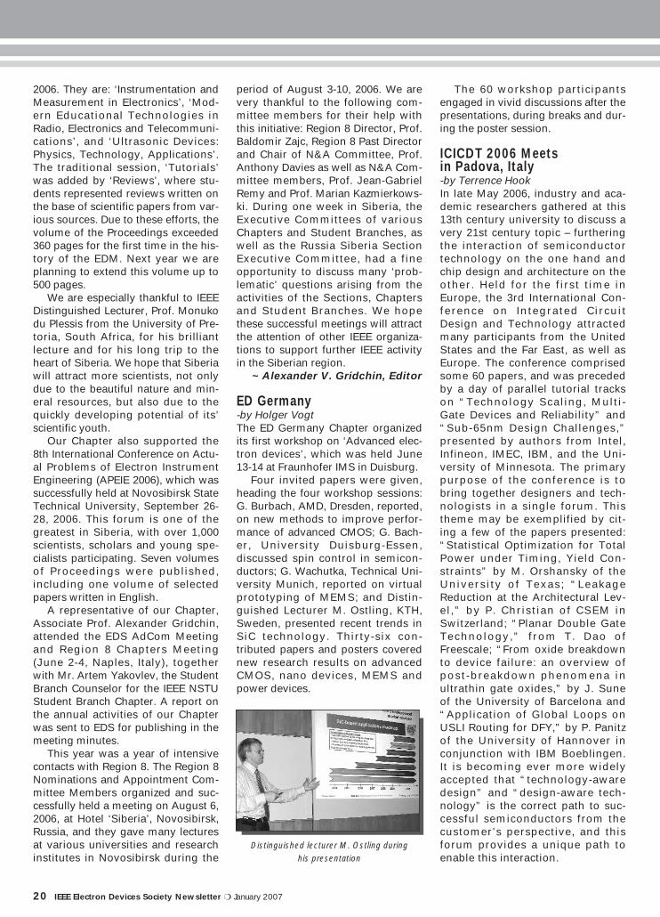
2006. They are: ‘Instrumentation andMeasurement in Electronics’, ‘Mod-ern Educational Technologies inRadio, Electronics and Telecommuni-cations’, and ‘Ultrasonic Devices:Physics, Technology, Applications’.The traditional session, ‘Tutorials’was added by ‘Reviews’, where stu-dents represented reviews written onthe base of scientific papers from var-ious sources. Due to these efforts, thevolume of the Proceedings exceeded360 pages for the first time in the his-tory of the EDM. Next year we areplanning to extend this volume up to500 pages.
We are especially thankful to IEEEDistinguished Lecturer, Prof. Monukodu Plessis from the University of Pre-toria, South Africa, for his brilliantlecture and for his long trip to theheart of Siberia. We hope that Siberiawill attract more scientists, not onlydue to the beautiful nature and min-eral resources, but also due to thequickly developing potential of its’scientific youth.
Our Chapter also supported the8th International Conference on Actu-al Problems of Electron InstrumentEngineering (APEIE 2006), which wassuccessfully held at Novosibirsk StateTechnical University, September 26-28, 2006. This forum is one of thegreatest in Siberia, with over 1,000scientists, scholars and young spe-cialists participating. Seven volumesof Proceedings were published,including one volume of selectedpapers written in English.
A representative of our Chapter,Associate Prof. Alexander Gridchin,attended the EDS AdCom Meetingand Region 8 Chapters Meeting(June 2-4, Naples, Italy), togetherwith Mr. Artem Yakovlev, the StudentBranch Counselor for the IEEE NSTUStudent Branch Chapter. A report onthe annual activities of our Chapterwas sent to EDS for publishing in themeeting minutes.
This year was a year of intensivecontacts with Region 8. The Region 8Nominations and Appointment Com-mittee Members organized and suc-cessfully held a meeting on August 6,2006, at Hotel ‘Siberia’, Novosibirsk,Russia, and they gave many lecturesat various universities and researchinstitutes in Novosibirsk during the
period of August 3-10, 2006. We arevery thankful to the following com-mittee members for their help withthis initiative: Region 8 Director, Prof.Baldomir Zajc, Region 8 Past Directorand Chair of N&A Committee, Prof.Anthony Davies as well as N&A Com-mittee members, Prof. Jean-GabrielRemy and Prof. Marian Kazmierkows-ki. During one week in Siberia, theExecutive Committees of variousChapters and Student Branches, aswell as the Russia Siberia SectionExecutive Committee, had a fineopportunity to discuss many ‘prob-lematic’ questions arising from theactivities of the Sections, Chaptersand Student Branches. We hopethese successful meetings will attractthe attention of other IEEE organiza-tions to support further IEEE activityin the Siberian region.
~ Alexander V. Gridchin, Editor
ED Germany-by Holger VogtThe ED Germany Chapter organizedits first workshop on ‘Advanced elec-tron devices’, which was held June13-14 at Fraunhofer IMS in Duisburg.
Four invited papers were given,heading the four workshop sessions:G. Burbach, AMD, Dresden, reported,on new methods to improve perfor-mance of advanced CMOS; G. Bach-er, University Duisburg-Essen,discussed spin control in semicon-ductors; G. Wachutka, Technical Uni-versity Munich, reported on virtualprototyping of MEMS; and Distin-guished Lecturer M. Ostling, KTH,Sweden, presented recent trends inSiC technology. Thirty-six con-tributed papers and posters coverednew research results on advancedCMOS, nano devices, MEMS andpower devices.
The 60 workshop participantsengaged in vivid discussions after thepresentations, during breaks and dur-ing the poster session.
ICICDT 2006 Meets in Padova, Italy-by Terrence HookIn late May 2006, industry and aca-demic researchers gathered at this13th century university to discuss avery 21st century topic – furtheringthe interaction of semiconductortechnology on the one hand andchip design and architecture on theother. Held for the first time inEurope, the 3rd International Con-ference on Integrated CircuitDesign and Technology attractedmany participants from the UnitedStates and the Far East, as well asEurope. The conference comprisedsome 60 papers, and was precededby a day of parallel tutorial trackson “Technology Scaling, Multi-Gate Devices and Reliability” and“Sub-65nm Design Challenges,”presented by authors from Intel,Infineon, IMEC, IBM, and the Uni-versity of Minnesota. The primarypurpose of the conference is tobring together designers and tech-nologists in a single forum. Thistheme may be exemplified by cit-ing a few of the papers presented:“Statistical Optimization for TotalPower under Timing, Yield Con-straints” by M. Orshansky of theUniversity of Texas; “LeakageReduction at the Architectural Lev-el,” by P. Christian of CSEM inSwitzerland; “Planar Double GateTechnology,” from T. Dao ofFreescale; “From oxide breakdownto device failure: an overview ofpost-breakdown phenomena inultrathin gate oxides,” by J. Suneof the University of Barcelona and“Application of Global Loops onUSLI Routing for DFY,” by P. Panitzof the University of Hannover inconjunction with IBM Boeblingen.It is becoming ever more widelyaccepted that “technology-awaredesign” and “design-aware tech-nology” is the correct path to suc-cessful semiconductors from thecustomer’s perspective, and thisforum provides a unique path toenable this interaction.
Distinguished lecturer M. Ostling during his presentation

January 2007 ❍ IEEE Electron Devices Society Newsletter 21
ISPSD 2006-by Paolo SpiritoThe 18th International Symposium onPower Semiconductor Devices and IC’s(ISPSD ’06) was held in Naples, Italy,June 4-8, 2006, returning to Europe forthe fifth time, with an attendance ofabout 350 people. This conference isthe major international forum in theareas of power semiconductor devices,from low voltage to high voltage dis-crete power devices, from modules tointegrated power, from silicon to newmaterials like SiC. One hundred paperswere selected from the 173 submitted;of these 18% from USA, 30% fromAsia, 50% from Europe. The confer-ence was preceded by a short courseon Sunday, June 4th, dedicated to“Electro-thermal management in Pow-er Devices and IC’s”.
The three invited talks featured onMonday, June 5, were dedicated to dif-ferent aspects of power applications,respectively on “Trend and Challengesin Automotive Electronics”, “PowerDrive Circuits for Diagnostic MedicalUltrasound”, and “Future Trend of FlatPanel Displays and Comparison of itsDriving Methods”. The award for beststudent paper was given to “A Digital-ly Controlled DC-DC Converter Modulewith a Segmented Output Stage forOptimized Efficiency” by O. Trescases,W.T. Ng, H. Nishio, M. Edo and T.Kawashima, of the University ofToronto, Canada and the Fuji ElectricAdvanced Technology Co., Japan.
More information can be found onthe official web site of the confer-ence: www.ISPSD2006.it.
ED Central/South Italy-by Salvatore Bellone and Heinz-Christoph NeitzertDuring the last year our chapter con-tinued the tradition of inviting inter-national lecturers to hold seminarsfocused on the microelectronic andoptoelectronic field. The cycle start-ed with a two-day course held byProf. C. Boit from Berlin TechnicalUniversity (Germany) at Salerno Uni-versity regarding “New generationSilicon & Diagnosis of ICs with phys-ical Techniques through Chip Backsurface”, by attracting more than 30graduated and post-graduated stu-dents. Dr. J. Bruns from Berlin Tech-nical University (Germany) held alecture on integrated optical technol-ogy, and Dr. Y. Ma from the Fernuni-versitaet Hagen (Germany) gave aseminar on solar cell technology.The cycle of seminars concludedwith a lecture from M.K. Jayarajfrom Cochin University (India)regarding material science aspects ofoptoelectronic devices. All of theseseminars were addressing a mixedaudience consisting of students andresearchers from inside and outsidethe university.
To increase the attraction ofundergraduate students towards themicroelectronics field, in conjunctionwith the Student Branch of Salerno,during April 2006, the ED Chaptersupported and organized the partici-pation of ten undergraduate studentsto the two-week course, organized by
the “Micron D-RAM & CMOS Sen-sors Imager Fab” (Italy). The coursewas attended by selections of ten stu-dents from five universities in Central& South Italy (Cassino, L’Aquila,Napoli, Perugia, and Salerno). It wasintended to bring the students nearthe more sophisticated semiconduc-tor manufacturing facilities, in strictcontact with the Micron staff. Theopportunity for a longer period of jobtraining has been offered by Micronto those students who drew majorbenefits from the course. The rele-vance of this event was that itreceived good resonance in local andnational newspapers and has alsobeen seen in the background of thecurrent changes to the ElectricalEngineering curriculum. It follows thereform of studies introduced in Italyin 2002, which substituted the tradi-tional five-year course with a three-year, first level degree (bachelor),followed eventually by the two-yearMasters degree. To guarantee a suc-cessful application of the reform,increased interaction between indus-try and university is required, whichpromotes the entry of first level stu-dents into the labor market and theapplication of the culture of “Life-Long-Learning”, suggested by thereform. It should also be noted thatthe number of student memberswithin the chapter and the studentbranch increased considerably due tothe strong demand of participants forthe course.
Impression of the ISPSD in Naples Participants to the two week course at MICRON

22 IEEE Electron Devices Society Newsletter ❍ January 2007
IWCE-11-by Hans KosinaThe eleventh International Workshopon Computational Electronics (IWCE-11) was held on May 25-27 2006, at theTU Wien, Austria. Over the years, theworkshop has become the main inter-national forum for discussions on cur-rent trends and future directions forcomputational electronics. This year,220 researchers from 27 countries par-ticipated, which is a record for thismeeting, held periodically since 1992.The scientific program of IWCE-11 cov-ered traditional topics of TechnologyCAD, Monte Carlo and moleculardynamics methods, optical processes,quantum transport as well as emergingareas of molecular and organic elec-tronics and nano-bio electronics. Eightinvited lectures, 43 contributed talks,and 135 poster presentations were giv-en. The first invited presentation givenby Dr. Thomas Skotnicki from STMi-croelectronics, focused on the perspec-tive from industry. The future of CMOStechnology and where industry needsacademia was discussed. One of thefounders of IWCE, Prof. Karl Hess fromthe University of Illinois at Urbana,summarized the state-of-the-art of bio-logical ion channel simulation usingcomputational electronics methods. Acompanion workshop on Modeling ofReliability Issues was held the daybefore IWCE-11. Special focus hasbeen put on bias temperature instabili-ty (NBTI and PBTI). Eleven invitedspeakers summarized their findings.More information is available onwww.iwce.org.
WoDiM2006-by Salvatore LombardoThe 14th Workshop on Dielectricsin Microelectronics (WoDiM 2006)was held June 26-28, in SantaTecla (Catania), Italy, hosted byConsigl io Nazionale del le Ric-erche (CNR), with the support ofSTMicroelectronics, ConsorzioCatania Ricerche, University ofCatan ia , and o f the Catan iaRegional County. The meeting(see h t tp : / /www. imm. cnr . i t /wodim_2006/ index.htm), orga-nized by Salvatore Lombardo ofthe Istituto per la Microelettroni-ca e Microsistemi (IMM) and anin ternat iona l commit tee wi thmembers of CNR, CNRS, Fraun-hofer, IHP, Infineon, NMRC, NIST,Philips, ST, and the Universitiesof Barcelona and Padova, hasbeen attended by about 150 sci-ent is ts coming f rom Europe ,USA, and Far East, 21 countriesin total.
During the three days durationof the workshop, about 100 papersfocused on the theme ofdielectr ics in microelectronicswere presented. Subjects particu-larly discussed were in the field ofhigh-k dielectrics for CMOS andnon volatile memories, ultra-thinoxynitrides, novel memory con-cepts, insulators for BEOL process-es and novel substrates, and newapplications.
The next WoDiM will be organizedby IHP in Germany, and held in theBerlin area in 2008.
WOLTE-7 -by Bruno LeoneThe Seventh Workshop on Low Tem-perature Electronics (WOLTE-7) washeld on June 21-24, 2006, at the Euro-pean Space Research and TechnologyCentre of the European Space Agency(ESA-ESTEC) in Noordwijk, the Nether-lands. WOLTE celebrates its first year asthe International Workshop on LowTemperature Electronics, replacing theformer European Workshop on LowTemperature Electronics which wasfounded in 1994. Participants and orga-nizers from more than 16 countries andseveral more nationalities from aroundthe world, were represented this year.
WOLTE continues to attract special-ists from very disparate fields within“low-temperature electronics” as itsmain aim is to encourage interdiscipli-nary discussions. This year the work-shop hosted about 50 participants andfeatured 33 talks, 4 of which were invit-ed, and 13 posters. Among the topicspresented were: low-temperature elec-tronics using both Si and other tech-nologies such as, for instance, SiGe;cryogenic performance of optoelec-tronics components; superconductingelectronics; detectors, including instru-ments; MEMs; and applications,including many space applications, nodoubt thanks to the fact that the work-shop was hosted by the EuropeanSpace Agency.
The next International WOLTEworkshop is expected to take place in2008. The venue will be confirmed ata later date.
~ Cora Salm, Editor
“IWCE-11: The two poster sessions attracted many participants” Participants of the WOLTE workshop in Noordwijk

January 2007 ❍ IEEE Electron Devices Society Newsletter 23
ED Japan- by Atsushi KurobeOn Sept. 6, 2006, a DL meeting washeld at Tokyo Institute of Technology,Yokohama. Two DLs gave lectures onrecent interesting technologies. Prof.Hei Wong, who is from City Universi-ty of Hong Kong, China, talked aboutthe theoretical analysis of new High-K MOS gate dielectric films. The titleof his lecture was “Band structure,barrier heights, carrier effectivemasses and current conduction inhafnium and zirconium oxide films.”Prof. Cary Yang, who is from SantaClara University, USA, talked aboutthe physics and future applications of
carbon nanofibers, in a lecture enti-tled “Carbon nanofibers as on-chipinterconnect and thermal interfacematerials.” Both presentationsoffered the attendees the opportunityto get to grips with up-to-date, inter-esting and useful research. The meet-ing, with 20 participants, was verysuccessful.
In addition, the ED Japan Chapterorganized a symposium entitled,“Challenges and problems in Nano-CMOS technology toward the next 15years”, on Sept. 11, 2006, at WasedaUniversity in Tokyo. Seventeenspeakers gave talks on technologytrends, device, processes, materialanalysis, circuits and so on, whichwere all focused on the coming nano-electronics era. The symposium con-cluded with a panel discussion. Six
panelists, who were Prof. H. Iwai(Tokyo Institute of Tech.), Prof. K.Natori (Tsukuba Univ.) and Prof. M.Koyanagi (Tohoku Univ.), Prof. K.Yamada (Waseda Univ), Prof. T.Hiramoto (Univ. of Tokyo) and Dr. T.Chikyo (National Institute for Materi-als Science), engaged in fruitful dis-cussion on technologies 15 yearsfrom now. Topics were “What will bethe main nanoelectronics devices?”,“Will emerging devices replaceCMOS devices?” and “What shouldwe do from now on to achieve nano-electronics?” The symposium wasvery successful with more than 80participants.
ED Kansai- by Michinori NishiharaThe ED Kansai Chapter held a Distin-guished Lecture on July 11, 2006, onthe Toyonaka Campus of Osaka Uni-versity, by inviting Dr. Yoshiaki Hagi-wara, an IEEE Fellow and SONYFellow. Dr. Hagiwara has been a keycontributor to CCD image sensortechnology as well as SONY videoproducts, which utilize these devices.
His talk began with basic semicon-ductor physics and he explained itwithout using equations, but withintuitive descriptions of electrons andholes. He showed potential of imagerapplications, such as for use as eyesfor robots. He also spoke about howfundamental device technologyresearch and development canimpact our society and our owncareer as engineers. His talk attractedmuch attention from the young stu-dents of Osaka University, who madeup the majority of the 62 attendees. Itwas another successful and stimulat-ing DL meeting in ED Kansai.
ASIA & PACIFIC(REGION 10)
ASIA & PACIFIC(REGION 10)
The DL meeting on Sept. 6, 2006. From the second person from the left at the back: Prof. Hei Wong,City Univ. of Hong Kong; Prof. Hiroshi Iwai, Partner and EDS Jr. Past President; Prof. Cary Yang,
Santa Clara Univ.; Dr. Atsushi Kurobe, ED Japan Chapter Chair
The panel discussion in the symposium on “Challenges and Problems in Nano-CMOS Technology toward the next 15 years.” From the left: Prof. H. Iwai,Tokyo Institute of Tech.; Prof. K. Yamada, Waseda Univ.; Prof. T. Hiramoto, Univ. of Tokyo; Dr. T. Chikyo, National Institute for Materials Science; Prof. K.
Natori, Tsukuba Univ.; Prof. M. Koyanagi, Tohoku University
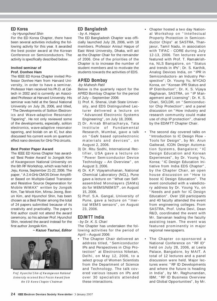
24 IEEE Electron Devices Society Newsletter ❍ January 2007
ED Korea- by Hyungcheol ShinFor the ED Korea Chapter, there havebeen several activities including the fol-lowing activity for this year. It awardedthe best poster award at the KoreanConference on Semiconductors. Theactivity is specifically described below.
Invited seminar of Prof. Donhee HamThe IEEE ED Korea Chapter invited Pro-fessor Donhee Ham from Harvard Uni-versity, in order to have a seminar.Professor Ham received his Ph.D. at Cal-tech in 2002 and is currently an Associ-ated Professor at Harvard University. Hisseminar was held at the Seoul NationalUniversity on July 26, 2006, and titled,“The Developments of Soliton Electron-ics and Wave-adaptive ResonatorTapering”. He not only reviewed someof the developments, especially, solitonelectronics, wave-adaptive resonatortapering, and biolab on an IC, but alsodiscussed his current work on quantumeffect nano devices for GHz-THz circuits.
Best Poster Paper AwardThe IEEE ED Korea Chapter has award-ed ‘Best Poster Award’ to Jongsik Kimof Kwangwoon National University onthe 6th RF Workshop, which was held inJeju, Korea, September 21-22, 2006. Thepaper, “A 2.4-GHz CMOS Driver Amplifi-er Based on Multiple-Gated Transistorand Resistive Source Degeneration forMobile WiMAX” written by JongsikKim, Tae Wook Kim, Minsu Jeong, Boe-un Kim, and Hyunchol Shin, has beenchosen as a Best Poster among the totalof 24 papers submitted because of itscreativity and practicality. The paper’sfirst author could not attend the awardceremony, so his adviser Prof. HyuncholShin, received the award instead for thefirst author Jongsik Kim.
~ Kazuo Tsutsui, Editor
ED Bangladesh- by A. HaqueThe ED Bangladesh Chapter was offi-cially launched July 28, 2006, with 18members. Professor Anisul Haque ofEast West University, Dhaka, will actas the Chapter Chair for the remainderof 2006. One of the priorities of theChapter is to increase the number ofstudent members and to motivate thestudents towards the activities of EDS.
AP/ED Bombay-by Mahesh PatilBelow is the quarterly report for theAP/ED Bombay Chapter for the periodof July – September 2006:1) Prof. K. Shenai, Utah State Univer-
sity, and EDS Distinguished Lec-turer delivered a lecture on“Advanced Electronic SystemsEngineering”, on July 18, 2006.
2) Dr. Arnab Bhattacharya, TataInst i tute of FundamentalResearch, Mumbai, gave a talkon “GaN based optoelectronicmater ia ls and devices”, onAugust 2, 2006.
3) Dr. Ritu Sodhi, International Rec-tifier, USA gave a lecture on“Power Semiconductor DeviceTechnology – An Overview”, onAugust 3, 2006.
4) Dr. K.P. Vijayamohanan, NationalChemical Laboratory (NCL), Punegave a lecture on “What can Self-assembled Monolayers (SAMs)do for MEMS/NEMS?”, on August15, 2006.
5) Prof. S.A. Gangal, University ofPune, gave a lecture on “Iner-tial MEMS sensors”, on August23, 2006.
ED/MTT India- by Dr. K. S. ChariThe Chapter has undertaken the fol-lowing activities for the period ofApril – August 2006:• The Chapter Chair delivered an
address titled, “SemiconductorIPs and Perspectives in Chip Pro-tection” at Electronics Niketan,Delhi, on May 12, 2006, to aselect group of Women Scientistsfrom the Department of Scienceand Technology. The talk cov-ered various issues on IPs andover 30 specialists attendedthese interactions.
• Chapter hosted a two day Nation-al Workshop on “IntellectualProperty Protection in Semicon-ductor Chips” at SASTRA, Than-javur, Tamil Nadu, in associationwith TIFAC - CORE during July12-13, 2006. Ten lectures werefeatured with Prof. T. Ramakrish-na, NLS Bangalore, on “Statusand trends in IPs”; Dr. S. Karthik,Analog Devices India, on “IPR inSemiconductors- an Industry Per-spective”; Dr. Young Yu, MYCADKorea, on “Korean IPR Status andIP Distribution”; Dr. K. S. VijayaRaghavan, SASTRA, on “IP Man-agement and Licensing”; Dr. K. S.Chari, SICLDR, on “Semiconduc-tor Chip Protection”; and a paneldiscussion on “How industry andresearch community could makeuse of chip IP protection”, chairedby the ED/MTT Chapter Chair.
• The second day covered talks on“Introduction to IC Design Flow -Tools for Design”, by Mr. ArunGaikwad, ICON Design Automa-tion Systems, Bangalore; “ICDesign Education and KoreanExperiences”, by Dr. Young Yu,Korea; “IC Design Education Ini-tiative from India EDS Chapter”,by the Chapter Chair, an openhouse discussion on “How toboost IC Design Education”. Theevent concluded with a valedicto-ry address by Dr. Young Yu, on“Needs and path for IC DesignEducation”. Over 150 participantsand 40 faculty attended the eventfrom engineering colleges. FromSASTRA, Prof. Usha Devi, DeanR&D, coordinated the event withMr. Sarvanan leading the facultyassisting team. The event wasfeatured prominently in majorregional newspapers.
• The Chapter co-sponsored aNational Conference on “RF ID”held on July 28, 2006, at LeelaPalace, Bangalore, by MAIT. Atotal of 12 lectures and a paneldiscussion were held. Major lec-tures were: “RF ID Developmentsand where the future is headingin India”, by Mr. Raghunandan,IBM; “RF ID Business Overviewand Global Opportunities”, by Mr.
Prof. Hyunchol Shin of Kwangwoon NationalUniversity received Best Poster Award from
the ED Korea Chapter Chairman

January 2007 ❍ IEEE Electron Devices Society Newsletter 25
Amit Phadnis; Symbol Technolo-gies India; “Fundamentals of RFID Implementation”, by Mr.Prasenjit Bhandra, IBM India;“Virgin Atlantic Airways- a casestudy”, by Mr. T.S. Rangarajan,TCS; “Technology Dynamics andProduct Innovations”, by Mr.Louis Kirk, Symbol Technologies;“Enhancing Business through RFID Innovation”, by Mr. Merlin Leo,Gemini Traze RF ID Ltd.; “RF ID inManufacturing”, by Mr. SrikumarNarayan, Winfoware Tech Ltd.;“RF ID-Cost vs Benefit” by Mr.Sreenath Venkappiah, WIPRO;“Consumer Privacy issues” byMr. Stephen Mathias, Kochharand Company; “RD ID Dynamics -Cost, Standards, Adoption etc”,by Mr. Puneet Gupta, InfosysTechnologies. Panel discussion“RF ID Prospects and Opportuni-ties in India” with panelists Mr.Pradhyumna Venkat, Mr. PuneetGupta, Mr. Prasenjit Bhadra andDr. K.S. Chari, ED/MTT ChapterChair, concluded the event whichattracted over 125 participants.Mr. D. Seetharam, IBM India Ltd.,Mr. Nanda Kumar and Mr. Premjitfrom MAIT Bangalore, coordinat-ed the event. The Conference’sprincipal sponsor was IBM India,with co-sponsors TRAZE, WINO-FARE, Symbol and supported bythe Department of IT, Karnataka.
• Chapter co-sponsored a TechnicalWorkshop on RFID Technologyheld in Pragati Maidan, New Delhi,on September 5, 2006. The eventfeatured two half-day sessions -RFID for Smart Card Applicationsdelivered by Dr. J.P. Benhammou,Atmel Corp., USA and RFID Tech-nology for Inventory Control andWarehouse Management deliveredby Mr. Rainer Lutz and Mr. Dhanan-jay Dixit from Philips Semiconduc-tors Austria and India. The talkspresented the respective technolo-gies, product solutions, standardsand demonstrations. Over 120 par-ticipants attended the lectures. Theevent was organized by ElectronicsToday, India, with many co-spon-sorships and coordinated by theEditor-in-Chief, Mr. S. Swaran.
• The Chapter co-sponsored two
International Conferences on“Emerging Technologies inMobile Communications” and“Trends in RFID Technology andApplications” on September 6and 7-8, 2006, respectively, atPragati Maidan, New Delhi. Co-located with the Conferences,“India Mobile Forum” and “RFIDIndia and Smart Card”, were heldwith 200 exhibitors from about 25countries participating andexhibiting their products and ser-vices. The exhibitions attractedthousands of visitors. Theseevents were organized by Elec-tronics Today and co-sponsoredby over 30 associations.
• Michael Lightner, IEEE President2006, delivered a lecture on “Cog-nitive Assistive Technology: AnEmerging Discipline”, at IIT Delhion May 1, 2006. The talk coveredthe aspects of cognitive disabili-ties, the assistive technologies,factors influencing the demandvis-à-vis technological options,smart home and caring familyconcepts, contest aware frame-works, etc. IEEE Delhi Section andthe Center for Biomedical Engi-neering, IIT, sponsored the talk.The ED/MTT Chapter Chair metwith IEEE President, MichaelLightner, and apprised him of the
STAR students at NFRC, Pedavegi
Attendees of the IPR workshop at SASTRA
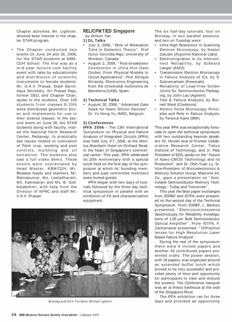
Chapter activities. Mr. Lightner,showed keen interest in the chap-ter STAR program.
• The Chapter conducted twoevents on June 24 and 26, 2006,for the STAR students at KBM-CGH School. The first was as amid-year lecture-cum-facilityevent with talks by educationistsand distribution of scientif icinstruments to female students.Mr. G.A.V. Prasad, State Sarvo-daya Secretary, Sri Prasad Raju,former DEO, and Chapter Chair,spoke to the students. Over 100students from classes 8-10thwere distributed geometric box-es and implements for use intheir science classes. In the sec-ond event on June 26, the STARstudents along with faculty, visit-ed the National Farm ResearchCenter, Pedavegi, to practicallysee issues related to cultivationof Palm crop, seeding and pestcontrols, mulching and oilextraction. The students alsosaw a full video demo. Theseevents were coordinated byHead Master, KBMCGH, Mr.Bhaskar Naidu and teachers, Mr.Ratnakumar, Ms. Leeladharani,Ms. Kameswari and Ms. B. Sub-balakshmi, with help from theDirector of NFRC and staff Mr.V.S.V. Prasad.
REL/CPMT/ED Singapore- by Wilson Tan1) DL Talks• July 3, 2006, “Role of Relaxation
Time in Dielectric Theory”, ProfGorur Govinda Raju, University ofWindsor, Canada.
• August 2, 2006, “Post-breakdownConduction in Ultra-thin GateOxides: From Physical Models toCircuit Applications”, Prof. EnriqueMiranda, Electronics Engineeringfrom the Universitat Autònoma deBarcelona (UAB), Spain.
2) Technical Talks• August 28, 2006, “Advanced Gate
Stack for Nano Silicon Devices”,Dr. Yu Hong Yu, IMEC, Belgium.
3) ConferencesIPFA 2006 - The 13th InternationalSymposium on Physical and FailureAnalysis of Integrated Circuits (IPFA)was held July 3-7, 2006, at the Meri-tus Mandarin Hotel on Orchard Road,in the heart of Singapore’s commer-cial center. This year, IPFA celebratedits 20th Anniversary with a speciallunch held on the first day of the sym-posium at which its’ founding mem-bers and past committee memberswere invited guests.
IPFA began with two days of tuto-rials followed by the three day tech-nical symposium in parallel with anexhibition of FA and characterizationequipment.
The six half-day tutorials, four onMonday, in two parallel sessions,and two on Tuesday were:• Ultra High Resolution in Scanning
Electron Microscopy, by NestorZaluzec (Argonne National Labs)
• Electromigration in Cu Intercon-nect Reliability, by EckhardLanger (AMD)
• Transmission Electron Microscopyin Failure Analysis of ICs, by S.Subramaniam (Freescale)
• Reliability of Lead-Free SolderJoints for Semiconductor Packag-ing, by John Lau (Agilent)
• Test & Failure Analysis, by Bur-nell West (Credence)
• Atomic Force Microscopy Princi-ples and Role in Failure Analysis,by Terence Kane (IBM)
This year IPFA was exceptionally fortu-nate to open the technical symposiumwith two outstanding keynote speak-ers: Dr. Hiroshi Iwai of Frontier Collab-orative Research Center, TokyoInstitute of Technology, and Jr. PastPresident of EDS, spoke on the “Futureof Nano-CMOS Technology and itsProduction” and Dr. Chih-Yuan Lu, Sr.Vice-President of Microelectronics &Memory Solution Group, Macronix Int.Co., gave a presentation on “Non-volatile Semiconductor Memory Tech-nology - Today and Tomorrow”.
This year the Best paper exchangesfrom ESREF and ISTFA were present-ed on the second day of the TechnicalSymposium. From ESREF, L. Bechoupresented, “ElectroluminescenceSpectroscopy for Reliability Investiga-tions of 1.55 µm Bulk SemiconductorOptical Amplifier”. From ISTFA, F.Zachariasse presented, “Diffractivelenses for High Resolution LaserBased Failure Analysis”.
During the rest of the symposiumthere were 6 invited papers andanother 44 contributed papers pre-sented orally. The poster session,with 18 papers, was organized aroundan extended buffet lunch whichproved to be very successful and pro-vided plenty of time and opportunityfor participants to view and discussthe posters. The Conference banquetwas an al fresco barbecue at the sideof the Singapore River.
The IPFA exhibition ran for threedays and provided an opportunity
26 IEEE Electron Devices Society Newsletter ❍ January 2007
Meeting with IEEE President, Michael Lightner

for 26 companies to show theirproducts and services. There wasalso an FIB user group meetingheld on Wednesday evening. Dur-ing the conference the call forpapers for IPFA 2007, to be held inBangalore, India, was announced.
A total of 146 registrations for theSymposium & 120 registrations forthe 2-day Tutorial, complementedthe 28 Exhibition booths that show-cased the latest products from 26participating companies.
The 2 best papers chosen are as follow:
Best Reliability Paper:7.1-3 Analysis of Failure Mecha-
nism on Gate-Silicided andG a t e - N o n - S i l i c i d e d ,Drain/Source Silicide-blocked
ESD NMOSFETs in a 65nmBulk CMOS TechnologyJ.J. Li1, D. Alvarez2, K. Chat-ty1, M.J. Abou-Khalil1, R. Gau-thier1, C. Russ3, C. Seguin1and R. Halbach1 / 1IBM Semi-conductor Research andDevelopment Center, USA2Infineon Technologies, USAand 3Infineon Technologies,Germany — Will be presentedat ESREF in October
Best Failure Analysis Paper:7.3-4 Distinction of Photo-Electric
and Thermal Effects in aMOSFET by 1064 nm LaserStimulationS.K. Brahma, J. Heinig, A.Glowacki, R. Leihkauf and C.Boit / Berlin University ofTechnology, Germany — Willbe presented at ISTFA inNovember
EPTC 2006The 8th Electronics PackagingTechnology Conference (EPTC2006) was held on December 6-8,2006, at the Pan Pacific Hotel Sin-gapore. It is an international con-ference event organized by theIEEE Reliability/CPMT/ED Singa-
pore Chapter and sponsored byIEEE CPMT Society. EPTC 2006 fea-tured technical sessions, shortcourses and exhibitions. The con-ference received a total of 194abstract submissions coming from22 countries. Further details can befound at the conference website(http://www.eptc-ieee.net).
~Xing Zhou, Editor
January 2007 ❍ IEEE Electron Devices Society Newsletter 27
Keynote speech by Professor Hiroshi Iwai
Keynote Speaker, Dr. Chih-Yuan Lu, receivinghis token of appreciation from General Chair,
Alastair Trig
• Amy A. Kruse, Director, DefenseAdvanced Research ProjectsAgency (DARPA), USA Topic: Military Applications of PID’s
• Iwona Turlik, Corporate VicePresident, Physical RealizationResearch, Motorola, Inc., USA Topic: Overview of PID’s
• Steve Kang, Dean of Engineer-ing, University of California -Santa Cruz, USA Topic: Nanotechnologies and PIDS
• Andrew Lippman, Senior ResearchScientist, Director, Digital Life, MITMedia Lab, USATopic: Viral Communications/Wearable Computers/ Digital TV
Additional invited speakers andpanelists include: Joe C. Barrett,Director, Intel Corporation, USA;Achintya Bhown, Manager, IntelCorporation, USA; Phil C H Chan,Chair Professor and Dean of Engi-neering, The Hong Kong Universityof Science and Technology, HongKong.; Mario El-Khoury, Vice-Presi-dent, Systems Engineering, SwissCenter for Electronic andMicrotechnology, Switzerland;Michael S. Lebby, President andCEO, Optoelectronics IndustryDevelopment Association, USA;Meyya Meyyappan, Director, Cen-ter for Nanotechnology, Ames
Research Center, USA; and JohnReagan, Professor Emeritus, TheUniversity of Arizona, USA.
IEEE PORTABLE 2007 joins IEEEMobile WiMax Symposium, spon-sored by the IEEE CommunicationsSociety and the IEEE Broadcast Tech-nology Society’s IEEE InternationalSymposium on Broadband Multime-dia Systems & Broadcasting 2007 as acomponent of IEEE @ CTIA WIRE-LESS 2007, an interdisciplinary eventco-located with CTIA WIRELESS 2007.
For complete program informa-tion, registration and hotel reserva-tions visit www.ieee-portable.org.
Debora KingstonSenior Meetings Manager
IEEE Communications SocietyNew York, NY, USA
(continued from page 1)
2007 IEEE International Conference on Portable
Information Devices
2007 IEEE International Conference on Portable
Information Devices

28 IEEE Electron Devices Society Newsletter ❍ January 2007
The EDS Distinguished Lecturer Program exists for the purpose of providing EDS Chapters with a list of quality lecturerswho can potentially give talks at local chapter meetings. To arrange for a lecture, the EDS chapters should contact theDistinguished Lecturer directly. A general guideline for the visit, but not the absolute rule, is that the lecturer should beable to include the meeting site with an already planned travel schedule at a small incremental cost to the travel plan.Alternatively, a prior coincident travel plan would not be required if the lecturer is already located within an approximatefifty mile radius of a meeting site. Although the concept of the program is to have the lecturers minimize travel costs bycombining their visits with planned business trips, EDS will help subsidize lecturer travel in cases where few/no lecturerswill be visiting an area and/or a chapter cannot pay for all the expenses for a lecturer trip. For a full listing of EDS Distin-guished Lecturers and travel plans please contact Laura Riello of the EDS Executive Office (Tel: 1-732-562-3927, Fax: 1-732-235-1626, E-Mail: [email protected]).
EDS DISTINGUISHED LECTURER PROGRAM
- LECTURERS RESIDING IN CENTRAL,
WESTERN & SOUTH WESTERN USA AND
LATIN AMERICA
ILESANMI ADESIDATel: +1 217 244 6379E-Mail: [email protected]: +1 217 244 6375- GaN Processing and Devices- Advanced Fabrication Techniques
for Heterostructure FETs- High Speed Optoelectronic
Integrated Receivers for FiberOptical Communications
RAMESH K. AGARWALTel: +1 314 935 6091E-Mail: [email protected]: +1 314 935 4014- Application of Computational Flu-
id Dynamics Based Technology toComputational Electromagnetics
- Application of CFD Based Tech-nology to Computational Electro-magnetics and SemiconductorDevice Simulations
- Numerical Simulation of PartialDifferential Equations (PDEs) offComputational Physics on ParallelComputers
MUHAMMAD ASHRAFUL ALAMTel: +1 765 494 5988E-Mail: [email protected]: +1 765 494 6441- Reliability Physics: How, when,
and why transistors break- Nanocomposites for
Macroelectronic Applications: A Novel material for large area in electronics (e.g. displays,radars, etc.)
- Theory of Nanobiosensors forinexpensive (differential) genomesequencing
NARAIN D. ARORATel: +1 408 715 8502E-Mail: [email protected]: N/A
ROBERT BAUMANNTel: +1 972 995 1432E-Mail: [email protected]: +1 972 995 2770- Radiation effects on devices- General device reliability
ZEYNEP CELIK-BUTLERTel: +1 817 272 1309E-Mail: [email protected]: +1 817 272 7458 - Scalable, Compact Noise
Models for Advanced and Bipolar Devices
- Infrared Sensors on Flexible Substrates (Smart Skin)
- Noise and Reliability in AdvancedMicroelectronic and Nanoelec-tronic Devices
ANTONIO CERDEIRAALTUZARRATel: +52 5 747 73780E-Mail: [email protected]: +52 5 574 77114- Device Modeling and Extraction
Procedures- The Non-linear harmonic Distor-
tion in devices and circuits
ROBERT S. CHAUTel: 1 503 613 6141E-Mail: [email protected]: N/A
YUHUA CHENGTel: +1 949 231 4623E-Mail:[email protected]: +1 949 483 6970- Device Modeling for Mixed-Sig-
nal/RF Circuit Design- The Influence and Modeling of
Process Variation and Device Mis-match for Analog/RF CircuitDesign
- Characterization and Modeling ofMOSFET Flicker Noise for RF ICDesign
VIKRAM L. DALALTel: +1 515 294 1077E-Mail: [email protected]: N/A- Photovoltaic Energy Conversion- Solar Energy Conversion- Nanocrystalline Si-based elec-
tronic materials and devices
SUPRIYO DATTATel: + 1 765 494-3511E-Mail: [email protected]: +1 765 494-2706
HECTOR J. DE LOS SANTOSTel: +1 310 259 0767E-mail: [email protected]: N/A
EDS DISTINGUISHED LECTURER PROGRAM
- LECTURERS RESIDING IN CENTRAL,
WESTERN & SOUTH WESTERN USA AND
LATIN AMERICA

- Applications and Trends in RFMEMS
- NanoMEMS
CARLOS H. DIAZTel: +1 408 382 8029E-Mail: [email protected]: +1 408 382 8181- CMOS Technology Trends for
MS-RF System-On-Chip- Sub 100nm CMOS Technology
ANANTH DODABALPURTel: +1 512 232 1890E-Mail: [email protected]: +1 512 471 8575- Organic and Polymer Electronics- Chemical sensors based on
organic semiconductors
PAUL E. DODDTel: +1 505 844-1447E-Mail: [email protected]: +1 505 844 2991
MAGALI ESTRADA DEL CUETO-Tel: +52 5 747 7000 E-Mail: [email protected]: +52 5 747 7114- Alternative Dielectrics for Ultra-
thin MOS Devices- Modeling Fabricataion and Char-
acteriziation of Amorphous andPolycristalline TFTs
- Dielectrics for SubmicrometricDevices
- Modeling of Amorphous andPolycrystalline TFTs
FRANCISCO J. GARCIA SANCHEZTel: +58 212 906 4010E-Mail: [email protected]: +58 212 906 4025- MOSFET Evolution and Trends - Parameter Extraction Techniques
in MOSFET Modeling- Applications of the Integral
Difference Function to ParameterExtraction
LARRY HORNBECKTel: +1 214 567 9844E-Mail: [email protected]: +1 214 567 5454
RENUKA P. JINDALTel: +1 337 482 6570E-Mail: [email protected]: +1 337 482 6569
- Approaching Fundamental Limitson Signal Detection: Devices andPrinciples
- Nano-FET Fluctuation Physics
ASHOK K. KAPOORTel: +1 650 856 4025E-Mail: [email protected]: N/A- Limitations to scaling of transistors- Growth of semiconductor
technology driven by the needs of the information technology
- BiCMOS Technology
DIM-LEE KWONGTel: +1 512 471 5922E-Mail: [email protected]: + 1 512 471 4345- Si NarrowWire CMOS devices &
their applications to BioSensors- High Speed Interconnect Using
CMOS Photonics - High-K/Metal Gate CMOS Technol-
ogy Challenges- Pushing CMOS Scaling via Novel
Materials Added to Si
JACK C. LEETel: +1 512 471 8423E-Mail: [email protected]: +1 512 471 8982- High-K Dielectrics for CMOS Appli-
cations- Alternative Channel Materials
TSU-JAE KING LIUTel: +1 510 643 9251E-Mail: [email protected]: +1 510 642 2739- Sustaining the Si Revolution- Challenges and Opportunities
MARK S. LUNDSTROMTel: +1 765 494-3515E-Mail: [email protected]: +1 765 494 6441- Nanoscale Transistors:
UltimateSilicon and Beyond- Nanowire/Nanotube Transistors:
Physics, Status, and Prospects - Nanotechnology: Now or Never?
KARTIKEYA MAYARAMTel: +1 541 737 2972E-Mail: [email protected]: N/A- Modeling and Analysis of Substrate
Noise Coupling in Mixed-Signal Ics
- Coupled Device and Circuit Sim-ulation
- Simulation of Multi-TechnologyMicro and Nano Systems
ENRIQUE MIRANDATel: +54 11 4631 7208E-Mail: [email protected]: +54 11 4331 0129- Reliability of ultra-thin gate
oxides- Conduction mechanisms in
dielectrics
ARTURO MORALES-ACEVEDOTel: +52 5 747-3781E-Mail:[email protected]: +52 5 747-7114- Fabrication of Silicon Oxynitride
Thin Films to be Applied In theMicroelectronics Industry
- Polycrystalline and AmorphousThin Films for PhotovoltaicDevices
ALI M. NIKNEJADTel: N/AE-Mail: [email protected]: N/A- RF and mm-wave device modeling
YOSHIO NISHITel: +1 650 723 9508E-Mail: [email protected]: N/A- Nanoelectronic Devices and
Materials- Nonvolatile Memory Devices and
Materials
ADELMO ORTIZ-CONDETel: +58 212 906 4010E-Mail: [email protected]: +58 212 906 4025- Modeling and Parameter
Extraction Techniques in Semiconductor Devices
- Evolution and Trends of SOIMOSFET
KAMESHWAR POOLLATel: +1 510 909 9640E-Mail: [email protected]: +1 510 486 2676- Metrology, Modeling, and
Control in Semiconductor Manufacturing
January 2007 ❍ IEEE Electron Devices Society Newsletter 29

30 IEEE Electron Devices Society Newsletter ❍ January 2007
January 6 - 10, 2007, T International Confer-ence on VLSI Design, Location: NIMHANSConvention Center, Bangalore, India, Contact: SUma Mahesh, E-Mail: [email protected],Deadline: 7/14/06, www: http://www.vlsicon-ference.com/
January 31 - February 2, 2007, T Spanish Con-ference on Electron Devices, Location: SanLorenzo de El Escorial, Madrid, Spain, Contact:Carlos Algora, E-Mail: [email protected],Deadline: 10/31/06, www: Not Available
February 19 - 24, 2007, T IEEE InternationalConference on the Experience of Designingand Application of CAD Systems in Micro-electronics, Location: Lviv Polytechnic NationalUniversity, Lviv, Ukraine, Contact: Vasyl Teslyuk, E-Mail: [email protected], Deadline:10/30/06, www: http://www.lp.edu.ua/CADSM
March 13 - 15, 2007, T National Radio Sci-ence Conference, Location: Ain Shams Univer-sity, Cairo, Egypt, Contact: Said E. El-Khamy,E-Mail: [email protected], Deadline:10/30/06, www: Not Available
March 19 - 22, 2007, @ International Confer-ence on Microelectronic Test Structures,Location: Takeda Hall, University of Tokyo, Bunkyo-ku, Japan, Contact: Yoichi Tamaki, E-Mail:[email protected], Deadline:9/15/06, www: http://www.ee.ed.ac.uk/ICMTS
March 25 - 27, 2007, * IEEE InternationalConference on Portable InformationDevices, Location: Orange County ConventionCenter, Orlando, FL, USA, Contact: DeboraKingston, E-Mail: [email protected], Deadline:7/15/06, www: http://www.ieee-portable.org/2007/
March 26 - 28, 2007, T IEEE InternationalSymposium on Quality Electronic Design,Location: Double Tree Hotel, San Jose, CA, USAContact: Ali Iranmanesh E-Mail: [email protected]: 10/23/06 www: www.isqed.org
March 28 - 29, 2007, T IEEE InternationalConference on RFID, Location: Gaylord Tex-an Resort & Convention Center, Grapevine, TX,
USA, Contact: Bichl ien Hoang, E-Mai l :[email protected], Deadline: 11/17/06,www: http://www.ieee-rfid.org/2007/
April 15 - 19, 2007, * IEEE InternationalReliability Physics Symposium, Location:Hyatt Regency Phoenix at Civic Plaza, Phoenix,AZ, USA, Contact: Edward Cole, Jr., E-Mail:[email protected], Deadline: Not Available,www: www.irps.org
April 20 - 21, 2007, T International SiberianConference on Control and Communica-tion, Location: Tomsk Polytechnic University, Tom-sk, Russia, Contact: Oleg Stukach, E-Mail:[email protected], Deadline: 1/23/07, www:http://www.comsoc.org/tomsk
April 23 - 25, 2007, T International Sympo-sium on VLSI Technology, Systems andApplications, Location: Ambassador HotelHsinchu, Hsinchu, Taiwan, Contact: Stacey Hsieh, E-Mail: [email protected], Deadline: 10/15/06,www: http://vlsitsa.itri.org.tw
April 25 - 27, 2007, T International Sym-posium on VLSI Design, Automation andTest, Location: Ambassador Hotel Hsinchu,Hsinchu, Taiwan, Contact: Elodie Ho, E-Mail:[email protected], Deadline: 10/15/06,www: http://vlsidat.itri.org.tw
April 30 - May 2, 2007, T IEEE Sarnoff Sympo-sium on Advances in Wired and WirelessCommunications, Location: Nassau Inn, Prince-ton, NJ, USA, Contact: Gerhard Franz, E-Mail:[email protected], Deadline: 12/4/06,www: http://www.sarnoffsymposium.org
May 7 - 10, 2007, T International Conferenceon Memory Technology and Design, Loca-tion: Village Vacances Familles (VVF) “La Badine”,Hyeres Les Palmiers, France, Contact: Liesbet Mas-sant, E-Mail: [email protected], Deadline: NotAvailable, www: http://www.icmtd.com
May 14 - 18, 2007, @ International Confer-ence on Indium Phosphide and RelatedMaterials, Location: Kunibiki Messe, Matsue,Japan, Contact: Shigehisa Arai, E-Mail:[email protected], Deadline: Not Available,
www: http://www.iprm.jp/index.html
May 14 - 17, 2007, T International Electrosta-tic Discharge Workshop, Location: StanfordSierra Conference Center, South Lake Tahoe, CA,USA, Contact: Lisa Pimpinella, E-Mail:[email protected], Deadline: 11/17/06, www:www.esda.org/iew.htm
May 15 - 17, 2007, @ IEEE International Vac-uum Electronics Conference, Location:Kitakyushu International Conference Center,Kitakyushu, Japan, Contact: Yoshie Moriguchi, E-Mail: [email protected], Deadline: 1/12/07,www: http://www.ivec2007.org
May 15 - 20, 2007, T IEEE Semiconductingand Insulating Materials Conference, Loca-tion: University of Arkansas, Fayetteville, AK, USA,Contact: Zhiming Wang, E-Mail:[email protected], Deadline: Not Available,www: http://www.ibiblio.org/simc
May 23 - 26, 2007, T International Con-ference on Perspective Technologiesand Methods in MEMS Design ,Location: Lviv Polytechnic National Universi-ty, Lviv, Ukraine, Contact: Mykola Pereyma,E-Mail: [email protected], Deadline:2/1/07, www: http://www.lp.edu.ua/Insti-tute/IKN/CAD/MEMSTECH
May 27 - 31, 2007, @ IEEE International Sym-posium on Power Semiconductor Devices& Integrated Circuits, Location: Ramada PlazaJeju Hotel, Jeju, South Korea, Contact: Min-KooHan, E-Mail: [email protected], Deadline: Not Avail-able, www: http://www.ispsd07.org
May 29 – June 1, 2007, T International Con-ference on Electron, Ion and PhotonBeam Technology and Nanofabrication,Location: Adam’s Mark Hotel, Denver, Colorado,Contact: Gregory M. Wallraff, E-Mail:[email protected], Deadline: 1/12/07,www: http://www.eipbn.org
June 3 - 5, 2007, T IEEE Radio FrequencyIntegrated Circuits Symposium, Location:Hawaii Convention Center, Honolulu, HI,USA, Contact: Luciano Boglione, E-Mail:
The complete EDS Calendar can be found at our web site:http://www.ieee.org/society/eds/meetings/meetings_calendar.xml Please visit!
EDS MEETINGS CALENDAR(As of November 15, 2006)
EDS MEETINGS CALENDAR(As of November 15, 2006)
January 2007 ❍ IEEE Electron Devices Society Newsletter 31
l [email protected], Deadline: 1/8/07,www: http://www.rfic2007.org
June 5 - 7, 2007, * IEEE International Inter-connect Technology Conference, Location:Hyatt Regency at San Francisco Airport,Burlingame, CA, USA, Contact: Wendy Walker, E-Mail: [email protected], Deadline:1/19/07, www: http://www.his.com/~iitc/
June 7 - 10, 2007, T IEEE Workshop onCharge-Coupled Devices & AdvancedImage Sensors, Location: The Cliff House Resort& Spa, Ogunquit, ME, USA, Contact: BedabrataPain, E-Mail: [email protected], Deadline: NotAvailable, www: Not Available
June 8 - 9, 2007, T International Workshopon Junction Technology, Location: Kyoto Uni-versity Clock Tower Centennial Hall, Kyoto,Japan, Contact: Kazuo Tsutsui, E-Mail:[email protected], Deadline: 3/2/07, www:http://www.iwailab.ep.titech.ac.jp/IWJT/
June 10 - 14, 2007, @ TRANSDUCERS -International Conference on Solid-StateSensors, Actuators and Microsystems,Location: Cite Centre Des Congres, Lyon,France, Contact: Thomas Garmier, E-Mail:[email protected], Deadline: 12/1/06,www: www.transducers07.org
June 11 - 12, 2007, * IEEE/SEMI AdvancedSemiconductor Manufacturing, Confer-ence Location: Grand Hotel Bristol, Stresa, Italy,Contact: Margaret Kindling, E-Mail: [email protected], Deadline: 10/19/06, www:http://www.semi.org/asmc
June 12 - 15, 2007, @ IEEE Symposium onVLSI Technology, Location: Rihga Royal Hotel,Kyoto, Japan, Contact: Phyllis Mahoney, E-Mail:[email protected], Deadline: Not Available,www: http://www.vlsisymposium.org
June 20 - 23, 2007, T Conference on Insulat-ing Films on Semiconductors, Location: Glyfa-da, Athens, Greece, Contact: Athanasios Dimoulas,E-Mail: [email protected], Deadline: NotAvailable, www: http://www.infos2007.gr
June 21 - 23, 2007, T International MIXDESConference, Location: Targon Palace,Ciechocinek, Poland, Contact: Andrzej Napieral-ski, E-Mail: [email protected], Deadline:2/28/07, www: http://www.mixdes.org
June 26 - 29, 2007, T International Sympo-sium on Physics & Engineering of Millime-ter & Sub-Millimeter Waves, Location: Kharkiv
National University, Sharkiv, Ukraine, Contact:Alexander Nosich, E-Mail: [email protected],Deadline: Not Available, www:http://www.ire.kharkov.ua/MSMW07
July 1 - 5, 2007, T International SiberianWorkshop and Tutorial on Electron Devicesand Materials, Location: Novosibirsk State Tech-nical University, Novosibirsk, Russia, Contact:Alexander Gridchin, E-Mail: [email protected],Deadline: 3/15/07, www: www.nstu.ru/edm
July 8 - 12, 2007, @ International VacuumNanoelectronics Conference, Location: HolidayInn Chicago Mart Plaza, Chicago, IL, USA, Contact:Heinz Busta E-Mail: [email protected],Deadline: Not Available, www: Not Available
July 11 - 13, 2007, T IEEE InternationalSymposium on the Physical and FailureAnalysis of Integrated Circuits, Location:Bangalore, India, Contact: M. Radhakrishnan, E-Mail: [email protected], Deadline:1/15/07, www: http://www.ieee.org/ipfa
August 21 - 24, 2007, T Topical Workshopon Heterostructure Microelectronics,Location: Kazusa Arc, Kisarazu-shi, Chiba,Japan, Contact: Takatomo Enoki, E-Mail: [email protected], Deadline: Not Available,www: http://www.twhm.net/
August 26 - 30, 2007, @ IEEE Non-VolatileSemiconductor Memory Workshop,Location: Hyatt Regency Monterey, Monterey, CA,USA, Contact: Stephen Keeney, E-Mail:[email protected], Deadline: 5/25/07,www: http://www.ewh.ieee.org/soc/eds/nvsmw/
September 9 - 14, 2007, T International Con-ference on Noise in Physical Systems and1/F Fluctuations, Location: National Institute forYouth Education, Shibuya-ku, Tokyo, Japan,Contact: Munecazu Tacano, E-Mail:[email protected], Deadline: Not Available,www: http://icnf.meisei-u.ac.jp/
September 10 - 14, 2007, T European Solid-State Device Research Conference, Loca-tion: TU Muenchen Arcisstrasse, Munich,Germany, Contact: Philip Teichmann E-Mail:[email protected], Deadline: Not Available,www: http://www.essderc.org/
September 16 - 19, 2007, T IEEE CustomIntegrated Circuits Conference, Location:Double Tree Hotel, San Jose, CA, USA, Con-tact: Melissa Widerkehr, E -Mai l :[email protected], Deadline: Not Avail-able, www: http://www.ieee-cicc.org
September 17 - 21, 2007, T International Con-ference on Electromagnetics in AdvancedApplications, Location: Torino Incontra CongressCenter, Torino, Italy, Contact: Guido Lombardi, E-Mail: [email protected], Deadline: Not Available,www: www.iceaa.polito.it
September 25 - 27, 2007, @ IEEE InternationalConference on Simulation of Semiconduc-tor Processes and Devices, Location: TU Vien-na, Vienna, Austria, Contact: Tibor Grasser, E-Mail:[email protected], Deadline: 3/1/07,www: http://www.sispad.org
September 30 - October 3, 2007, T IEEE Confer-ence on Intelligent Transportation Systems,Location: Hilton Hotel, Bellevue, WA, USA, Contact:Paul Kostek, E-Mail: [email protected], Deadline:3/1/07, www: http://www.ewh.ieee.org/tc/its/
September 30 - October 2, 2007, @ IEEE Bipo-lar/BiCMOS Circuits and Technology Meet-ing, Location: Boston Marriott Long Wharf, Boston,MA, USA, Contact: Janice Jopke, E-Mail:[email protected], Deadline: 3/1/07, www:www.ieee-bctm.org
October 7 - 12, 2007, T Symposium onULSI Process Integration, Location: Wash-ington, DC, USA, Contact: Cor Claeys, E-Mail:[email protected], Deadline: 5/26/07, www:Not Available
October 14 - 17, 2007, * IEEE CompoundSemiconductor IC Symposium, Location:Hilton Portland & Executive Tower, Portland, OR,USA, Contact: Mohammad Madihian, E-Mail:[email protected], Deadline: 5/7/07, www:http://www.csics.org/
November 4 - 8, 2007, T IEEE InternationalConference on Computer Aided Design,Location: DoubleTree Hotel San Jose, San Jose, CA,USA, Contact: Kathy MacLennan, E-Mail:[email protected], Deadline: Not Available,www: http://www.iccad.com
November 2007, T IEEE Electron Devices Activ-ities in Western New York Conference,Location: University of Rochester, Rochester, NY,USAk Contact: Karl Hirschmank E-Mail:[email protected] Deadline: Not Availablek www:Not Available
December 3 - 7, 2007, T International Pho-tovoltaic Science & Engineering Confer-ence, Location: Fukuoka International CongressCenter, Fukuoka, Japan, Contact: Yoshio Ohsita,E-Mail: [email protected], Deadline:7/15/07, www: http://www.pvsec17.jp

32 IEEE Electron Devices Society Newsletter ❍ January 2007
On August 21-25, 2006, the ED SouthBrazil Chapter and EDS StudentChapter at UNICAMP (State Univer-sity of Campinas), together withundergraduate students, organizedthe X Electrical Engineering Week2006 at the School of Electrical andComputer Engineering, in Campinas.About 400 participants attended the
meeting. Several lectures were giv-en by invited professors, industrymembers and personalities. In addi-tion to the industrial exposition, vis-its to local industries and researchcenters and a poster session werepart of the program, as can be seenat http://www.see.fee.unicamp.br.
A key lecture was presented by
Prof. Adelmo Ortiz Conde, from SimonBolivar University of Venezuela, as anIEEE EDS Distinguished Lecturer. Hislecture was entitled, “Evolution ofMOSFETs toward nanoelectronics”and was attended by more than 100participants.
The same lecture was also deliveredby Prof. Ortiz during the same week atthe School of Electrical Engineering ofthe UNESP (University of the State ofSão Paulo) in the city of Bauru.
Prof. Ortiz also gave a second lec-ture to a group of graduated studentsworking in the field of microelectron-ics, at the Center for SemiconductorComponents at UNICAMP, Campinas,focusing on modeling of MOS devices.
Jacobus W. SwartChapter Advisor
State University of CampinasCampinas, Brazil
Leandro T. ManeraPh. D. Student
UNICAMPCampinas, Brazil
EDS Distinguished Lecturer Visits
Universities in Brazil
IEEE EDS Distinguished Lecturer, Professor Adelmo Ortiz Conde, from Simon Bolivar University ofVenezuela, presenting his talk at the University of the State of São Paulo
EDS Distinguished Lecturer Visits
Universities in Brazil