Embed Size (px)
Citation preview

KSZ8441HL/FHLIEEE 1588v2 Precision Time Protocol-Enabled, 10/100 Mbps
Ethernet End-Point Connection with 8- or 16-Bit Host Bus Interface
Features
Management Capabilities
• Supports IP Header (IPv4)/TCP/UDP/ICMP Checksum Generation and Checking
• Supports IPv6 TCP/UDP/ICMP Checksum Gener-ation and Checking
• Supports IEEE 802.3x Full-Duplex Flow Control and Half-Duplex Backpressure Collision Flow Control
• MIB Counters for Fully Compliant Statistics Gath-ering: 34 Counters on the Ethernet Port, Port 1
• Loopback Modes for Remote Failure Diagnostics
Robust Ethernet PHY Port
• Integrated IEEE 802.3/802.3u-Compliant Ethernet Transceiver Supporting 10BASE-T and 100BASE-TX
• Copper and Fiber Mode Support in the KSZ8441FHL
• Copper Mode Support in the KSZ8441HL
• Auto-Negotiation: 10/100 Mbps, Full- and Half-Duplex
• Adaptive Equalizer
• Baseline Wander Correction
• On-Chip Termination Resistors and Internal Bias-ing for Differential Pairs to Reduce Power
• HP Auto MDI/MDI-X Crossover Support Eliminat-ing the Need to Differentiate between Straight or Crossover Cables in Applications
Ethernet MAC
• Internal Media Access Control (MAC) Unit
• 2 Kbyte Jumbo Packet Support
• MAC Filtering Function to Filter Unknown Unicast Packets
• Port 1 MAC Programmable as Either E2E or P2P Transparent Clock (TC) Port for 1588 Support
Comprehensive Configuration Registers Access
• Complete Register Access via the Parallel Host Interface
• Facility to Load MAC Address from EEPROM at Power-Up and Reset Time
• I/O Pin Strapping Facility to Set Certain Register Bits from I/O Pins at Reset Time
• Control Registers Configurable On-the-Fly
IEEE 1588v2 PTP and Clock Synchronization
• Fully Compliant with the Appropriate IEEE 1588v2 Precision Time Protocol
• One-Step or Two-Step Transparent Clock (TC) Timing Corrections
• End-to-End (E2E) or Peer-to-Peer (P2P) Trans-parent Clock (TC)
• Grandmaster, Master, Slave, Ordinary Clock (OC) Support
• IEEE1588v2 PTP Multicast and Unicast Frame Support
• Transports of PTP over IPv4/IPv6 UDP and IEEE 802.3 Ethernet
• Delay Request-Response and Peer Delay Mech-anism
• Ingress/Egress Packet Time Stamp Capture/Recording and Checksum Update
• Correction Field Update with Residence Time and Link Delay
• IEEE1588v2 PTP Packet Filtering Unit to Reduce Host Processor Overhead
• A 64-bit Adjustable System Precision Clock
• Twelve Trigger Output Units and Twelve Time Stamp Input Units Available for Flexible IEEE1588v2 Control of Seven Programmable GPIO[6:0] Pins Synchronized to the Precision Time Clock
• GPIO Pin Usage for 1 PPS Generation, Fre-quency Generation, Control Bit Streams, Event Monitoring, Precision Pulse Generation, Complex Waveform Generation
Host Interface
• Selectable 8- or 16-bit Wide Interface
• Supports Big- and Little-Endian Processors
• Indirect Data Bus for Data, Address, and Byte Enable to Access any I/O Registers and RX/TX FIFO Buffers
• Large Internal Memory with 12 Kbyte for RX FIFO and 6 Kbytes for TX FIFO
• Programmable Low, High, and Overrun Water-mark for Flow Control in RX FIFO
• Efficient Architecture Design with Configurable Host Interrupt Schemes to Minimize Host CPU Overhead and Utilization
• Queue Management Unit (QMU) Supervises Data Transfers Across This Interface
2018 Microchip Technology Inc. DS00002640A-page 1

KSZ8441HL/FHL
Power and Power Management• Single 3.3V Power Supply with Optional 1.8V, 2.5V, or 3.3V VDD I/O
• Integrated Low Voltage (~1.3V) Low-Noise Regu-lator (LDO) Output for Digital and Analog Core Power
• Supports IEEE P802.3az Energy Efficient Ether-net (EEE) to Reduce Power Consumption in Transceivers in LPI State
• Full-Chip Hardware or Software Power-Down (All Registers Value are Not Saved and Strap-In Value will Re-Strap After Releasing the Power-Down)
• Energy Detect Power-Down (EDPD), which Dis-ables the PHY Transceiver when Cables are Removed
• Wake-on-LAN Supported with Magic Packet™, Link State, and Configurable Wake-Up Packet Control
• Dynamic Clock Tree Control to Reduce Clocking in Areas Not in Use
• Power Consumption Less than 0.5W
Additional Features
• Single 25 MHz ±50 ppm Reference Clock Requirement
• Comprehensive Programmable Two LED Indica-tors Support for Link, Activity, Full-/Half-Duplex, and 10/100 Speed
• LED Pins Directly Controllable
• Industrial Temperature Range: –40°C to +85°C
• 64-Pin (10 mm x 10 mm) Lead-Free (RoHS) LQFP Package
Applications
• Industrial Ethernet Applications that Employ IEEE 802.3-Compliant MACs. (Ethernet/IP, Profinet, MODBUS TCP, etc)
• Real-Time Ethernet Networks Requiring Sub-Microsecond Synchronization over Standard Ethernet
• IEC 61850 Networks Supporting Power Substa-tion Automation
• Networked Measurement and Control Systems
• Industrial Automation and Motion Control Sys-tems
• Test and Measurement Equipment
DS00002640A-page 2 2018 Microchip Technology Inc.

KSZ8441HL/FHL
TO OUR VALUED CUSTOMERS
It is our intention to provide our valued customers with the best documentation possible to ensure successful use of your Microchipproducts. To this end, we will continue to improve our publications to better suit your needs. Our publications will be refined andenhanced as new volumes and updates are introduced.
If you have any questions or comments regarding this publication, please contact the Marketing Communications Department viaE-mail at [email protected]. We welcome your feedback.
Most Current Data SheetTo obtain the most up-to-date version of this data sheet, please register at our Worldwide Web site at:
http://www.microchip.com
You can determine the version of a data sheet by examining its literature number found on the bottom outside corner of any page. The last character of the literature number is the version number, (e.g., DS30000000A is version A of document DS30000000).
ErrataAn errata sheet, describing minor operational differences from the data sheet and recommended workarounds, may exist for cur-rent devices. As device/documentation issues become known to us, we will publish an errata sheet. The errata will specify therevision of silicon and revision of document to which it applies.
To determine if an errata sheet exists for a particular device, please check with one of the following:• Microchip’s Worldwide Web site; http://www.microchip.com• Your local Microchip sales office (see last page)
When contacting a sales office, please specify which device, revision of silicon and data sheet (include -literature number) you areusing.
Customer Notification SystemRegister on our web site at www.microchip.com to receive the most current information on all of our products.
2018 Microchip Technology Inc. DS00002640A-page 3

KSZ8441HL/FHL
DS00002640A-page 4 2018 Microchip Technology Inc.
Table of Contents
1.0 Introduction ..................................................................................................................................................................................... 52.0 Pin Description and Configuration ................................................................................................................................................... 93.0 Functional Description ................................................................................................................................................................... 164.0 Register Descriptions .................................................................................................................................................................... 575.0 Operational Characteristics ......................................................................................................................................................... 1556.0 Electrical Characteristics ............................................................................................................................................................. 1567.0 Timing Specifications .................................................................................................................................................................. 1598.0 Reference Circuit: LED Strap-In Pins .......................................................................................................................................... 1669.0 Reference Clock: Connection and Selection ............................................................................................................................... 16710.0 Selection of Isolation Transformers ........................................................................................................................................... 16811.0 Package Outline ........................................................................................................................................................................ 169Appendix A: Data Sheet Revision History ......................................................................................................................................... 170The Microchip Web Site .................................................................................................................................................................... 171Customer Change Notification Service ............................................................................................................................................. 171Customer Support ............................................................................................................................................................................. 171Product Identification System ............................................................................................................................................................ 172

KSZ8441HL/FHL
1.0 INTRODUCTION
1.1 General Terms and Conditions
The following is list of the general terms used throughout this document:
BIU - Bus Interface Unit The host interface function that performs code conversion, buffering, and the like required for communications to and from a network.
BPDU - Bridge Protocol Data Unit A packet containing ports, addresses, etc. to make sure data being passed through a bridged network arrives at its proper destination.
CMOS - Complementary Metal Oxide Semiconductor
A common semiconductor manufacturing technique in which positive and negative types of transistors are combined to form a current gate that in turn forms an effective means of controlling electrical current through a chip.
CRC - Cyclic Redundancy Check A common technique for detecting data transmission errors. CRC for Ethernet is 32 bits long.
DA - Destination Address The network address to which packets are sent.
DMA - Direct Memory Access A design in which memory on a chip is controlled independently of the CPU.
EMI - Electromagnetic Interference A naturally occurring phenomena when the electromagnetic field of one device disrupts, impedes or degrades the electromagnetic field of another device by coming into proximity with it. In computer tech-nology, computer devices are susceptible to EMI because electro-magnetic fields are a byproduct of passing electricity through a wire. Data lines that have not been properly shielded are susceptible to data corruption by EMI.
FCS - Frame Check Sequence See CRC.
FID - Frame or Filter ID Specifies the frame identifier. Alternately is the filter identifier.
GPIO - General Purpose Input/Output General Purpose Input/Output pins are signal pins that can be con-trolled or monitored by hardware and software to perform specific tasks.
IGMP - Internet Group Management Protocol
The protocol defined by RFC 1112 for IP multicast transmissions.
IPG - Inter-Packet Gap A time delay between successive data packets mandated by the net-work standard for protocol reasons. In Ethernet, the medium has to be "silent" (i.e., no data transfer) for a short period of time before a node can consider the network idle and start to transmit. IPG is used to correct timing differences between a transmitter and receiver. During the IPG, no data is transferred, and information in the gap can be discarded or additions inserted without impact on data integrity.
ISI - Inter-Symbol Interference The disruption of transmitted code caused by adjacent pulses affect-ing or interfering with each other.
Jumbo Packet A packet larger than the standard Ethernet packet (1500 bytes). Large packet sizes allow for more efficient use of bandwidth, lower overhead, less processing, etc.
MAC - Media Access Controller A functional block responsible for implementing the media access control layer which is a sub-layer of the data link layer.
MDI - Medium Dependent Interface An Ethernet port connection that allows network hubs or switches to connect to other hubs or switches without a null-modem, or cross-over, cable. MDI provides the standard interface to a particular media (copper or fiber) and is therefore “media dependent”.
2018 Microchip Technology Inc. DS00002640A-page 5
KSZ8441HL/FHL
MDI-X - Medium Dependent Interface Crossover
An Ethernet port connection that allows networked end stations (i.e., PCs or workstations) to connect to each other using a null-modem, or crossover, cable. For 10/100 full-duplex networks, an end point (such as a computer) and a switch are wired so that each transmitter con-nects to the far end receiver. When connecting two computers together, a cable that crosses the TX and RX is required to do this. With auto MDI-X, the PHY senses the correct TX and RX roles, elim-inating any cable confusion.
MIB - Management Information Base The MIB comprises the management portion of network devices. This can include things like monitoring traffic levels and faults (statis-tical), and can also change operating parameters in network nodes (static forwarding addresses).
MII - Media Independent Interface The MII accesses PHY registers as defined in the IEEE 802.3 speci-fication.
NIC - Network Interface Card An expansion board inserted into a computer to allow it to be con-nected to a network. Most NICs are designed for a particular type of network, protocol, and media, although some can serve multiple net-works.
NRZ - Non-Return to Zero A type of signal data encoding whereby the signal does not return to a zero state in between bits.
PHY - Physical Interface Device A device or functional block which performs the physical layer inter-face function in a network.
PLL - Phase-Locked Loop An electronic circuit that controls an oscillator so that it maintains a constant phase angle (i.e., lock) on the frequency of an input, or ref-erence, signal. A PLL ensures that a communication signal is locked on a specific frequency and can also be used to generate, modulate, and demodulate a signal and divide a frequency.
PME - Power Management Event An occurrence that affects the directing of power to different compo-nents of a system.
PTP - Precision Time Protocol A protocol, IEEE 1588 as applied to this device, for synchronizing the clocks of devices attached to a specific network.
QMU - Queue Management Unit Manages packet traffic between MAC/PHY interface and the system host. The QMU has built-in packet memories for receive and transmit functions called TXQ (Transmit Queue) and RXQ (Receive Queue).
SA - Source Address The address from which information has been sent.
TDR - Time Domain Reflectometry TDR is used to pinpoint flaws and problems in underground and aerial wire, cabling, and fiber optics. They send a signal down the conductor and measure the time it takes for the signal, or part of the signal, to return.
TSU - Time Stamp Input Unit The functional block which captures signals on the GPIO pins and assigns a time to the specific event.
TOU - Trigger Output Unit The functional block which generates user configured waveforms on a specified GPIO pin at a specific trigger time.
UTP - Unshielded Twisted Pair Commonly a cable containing four twisted pairs of wires. The wires are twisted in such a manner as to cancel electrical interference gen-erated in each wire, therefore shielding is not required.
DS00002640A-page 6 2018 Microchip Technology Inc.
KSZ8441HL/FHL
1.2 General Description
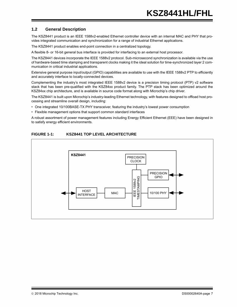
The KSZ8441 product is an IEEE 1588v2-enabled Ethernet controller device with an internal MAC and PHY that pro-vides integrated communication and synchronization for a range of industrial Ethernet applications.
The KSZ8441 product enables end-point connection in a centralized topology.
A flexible 8- or 16-bit general bus interface is provided for interfacing to an external host processor.
The KSZ8441 devices incorporate the IEEE 1588v2 protocol. Sub-microsecond synchronization is available via the useof hardware-based time stamping and transparent clocks making it the ideal solution for time-synchronized layer 2 com-munication in critical industrial applications.
Extensive general purpose input/output (GPIO) capabilities are available to use with the IEEE 1588v2 PTP to efficientlyand accurately interface to locally-connected devices.
Complementing the industry’s most integrated IEEE 1588v2 device is a precision timing protocol (PTP) v2 softwarestack that has been pre-qualified with the KSZ84xx product family. The PTP stack has been optimized around theKSZ84xx chip architecture, and is available in source code format along with Microchip’s chip driver.
The KSZ8441 is built upon Microchip’s industry-leading Ethernet technology, with features designed to offload host pro-cessing and streamline overall design, including:
• One integrated 10/100BASE-TX PHY transceiver, featuring the industry’s lowest power consumption
• Flexible management options that support common standard interfaces
A robust assortment of power management features including Energy Efficient Ethernet (EEE) have been designed into satisfy energy efficient environments.
FIGURE 1-1: KSZ8441 TOP LEVEL ARCHITECTURE
PRECISIONCLOCK
IEE
E 1
588v
2TI
ME
STA
MP
ING
PRECISIONGPIO
MAC 10/100 PHYHOSTINTERFACE
KSZ8441
2018 Microchip Technology Inc. DS00002640A-page 7

KSZ8441HL/FHL
FIGURE 1-2: SYSTEM BLOCK DIAGRAM, KSZ8441HL/FHL
EEPROMINTERFACE
VDD_IOVDD_L
INTRN
SD[15:0]
CMD
RDN
WRN
CSN
X1
X2
GPIOs
EEPROMINTERFACE
MIBCOUNTERS
IEEE 1588v2-ENABLEDHOST MAC
1.3V LOW-NOISEREGULATOR
HOST DATA BUS
INTERFACE UNIT
QMUANDDMA
CONTROL
TXQ6KB
RXQ12KB
I/O REGISTERSCONTROL/STATUS
IEEE 1588v2SYNCHRONIZED
CLOCK
PLL CLOCK
(TO 1588v2 TIMESTAMP
BLOCKS)
12 EVENT UNITSAND
12 TIMESTAMP UNITS
IEEE 1588v2TIMESTAMP FOR
PORT 1
10/100 BASET/TX/FXPHY 1
LinkMDAND EEE CONTROL
POWERMANAGEMENT
LED DRIVER
PORT 1TX/RX±
(AUTO MDI/MDI-X)
PME
P1LED[1:0]
DS00002640A-page 8 2018 Microchip Technology Inc.

KSZ8441HL/FHL
2.0 PIN DESCRIPTION AND CONFIGURATION
FIGURE 2-1: 64-PIN LQFP ASSIGNMENT, (TOP VIEW)
VD
D_I
OD
GN
DX2
X1
PW
RD
N
SD
15S
D14
SD
13
RXM1RXP1AGNDTXM1TXP1
VDD_ALISET
AGND
13141516
17 18 19 20
12345678
KSZ8441HL/FHL(TOP VIEW)
VDD_A3.3N/UN/U
AGND
9101112
SD
12S
D11
SD
10S
D9
21 22 23 24
363534333231302928272625
P1L
ED
0/H
816
N/U
LEB
ER
STN
FXS
D1
P1L
ED
1G
PIO
6D
GN
D
4847464544434241
VD
D_I
OG
PIO
5/E
EC
SG
PIO
4/E
ED
IOG
PIO
3/E
ES
K40393837
N/UN/UN/U
VDD_COL
GPIO0CSNPME/EEPROMWRNRDNINTRNCMDSD0VDD_LDGNDSD1SD2SD3SD4SD5SD6
GP
IO2
VD
D_L
DG
ND
GP
IO1
DG
ND
VD
D_I
OS
D8
SD
7
64 63 62 61 60 59 58 57 4950515253545556
2018 Microchip Technology Inc. DS00002640A-page 9

KSZ8441HL/FHL
TABLE 2-1: SIGNALS FOR KSZ8441HL/FHL
Pin Number
Pin NameType (Note2-1)
Description
1 RXM1 I/O Port 1 physical receive (MDI) or transmit (MDIX) signal (– differential).
2 RXP1 I/O Port 1 physical receive (MDI) or transmit (MDIX) signal (+ differential).
3 AGND GND Analog Ground.
4 TXM1 I/O Port 1 physical transmit (MDI) or receive (MDIX) signal (– differential).
5 TXP1 I/O Port 1 physical transmit (MDI) or receive (MDIX) signal (+ differential).
6 VDD_AL P This pin is used as an input for the low-voltage analog power. Its source should have appropriate filtering with a ferrite bead and capacitors.
7 ISET OSet physical transmits output current.Pull-down this pin with a 6.49 kΩ (1%) resistor to ground.
8 AGND GND Analog Ground.
9 VDD_A3.3 P 3.3V analog VDD input power supply (Must be well decoupled).
10 N/U I/O Not used. Do not connect anything to this pin.
11 N/U I/O Not used. Do not connect anything to this pin.
12 AGND GND Analog Ground.
13 N/U I/O Not used. Do not connect anything to this pin.
14 N/U I/O Not used. Do not connect anything to this pin.
15 N/U I This unused input should be connected to GND.
16 VDD_COL PThis pin is an input for the low-voltage analog power. Its source should have appropriate filtering with a ferrite bead and capacitors.
17 PWRDN IPU
Full-Chip Power-Down Active-Low (Low = Power-down; High or floating = Normal operation). While this pin is asserted low, all I/O pins will be tri-stated. All registers will be set to their default state. While this pin is asserted, power consumption will be minimal. When the pin is de-asserted, power consumption will climb to nomi-nal and the device will be in the same state as having been reset by the reset pin (RSTN, pin 63).
18 X1 I 25 MHz Crystal or Oscillator Clock ConnectionPins (X1, X2) connect to a crystal or frequency oscillator source. If an oscilla-tor is used, X1 connects to a VDD_IO voltage tolerant oscillator and X2 is a no connect. This clock requirement is ±50 ppm.
19 X2 O
20 DGND GND Digital ground.
21 VDD_IO P3.3V, 2.5V, or 1.8V digital VDD input power pin for IO logic and the internal low-voltage regulator.
22 SD15/BE3I/O
(PD)
Shared Data Bus Bit[15] or BE3: This is data bit (D15) access when CMD = “0”. This is Byte Enable 3 (BE3, 4th byte enable and active-high) at double-word boundary access in 16-bit bus mode when CMD = “1”. This pin must be tied to GND in 8-bit bus mode.
DS00002640A-page 10 2018 Microchip Technology Inc.

KSZ8441HL/FHL
23 SD14/BE2 I/O (PD)
Shared Data Bus Bit[14] or BE2: This is data bit (D14) access when CMD = “0”. This is Byte Enable 2 (BE2, 3rd byte enable and active-high) at double-word boundary access in 16-bit bus mode when CMD = “1”. This pin must be tied to GND in 8-bit bus mode.
24 SD13/BE1I/O
(PD)
Shared Data Bus Bit[13] or BE1: This is data bit (D13) access when CMD = “0”. This is Byte Enable 1 (BE1, 2nd byte enable and active-high) at double-word boundary access in 16-bit bus mode when CMD = “1”. This pin must be tied to GND in 8-bit bus mode.
25 SD12/BE0I/O
(PD)
Shared Data Bus Bit[12] or BE0: This is data bit (D12) access when CMD = “0”. This is Byte Enable 0 (BE0, 1st byte enable and active-high) at double-word boundary access in 16-bit bus mode when CMD = “1”. This pin must be tied to GND in 8-bit bus mode.
26 SD11I/O
(PD)Shared Data Bus Bit[11]: This is data bit (D11) access when CMD = “0”. Don’t care when CMD = “1”. This pin must be tied to GND in 8-bit bus mode.
27 SD10/A10I/O
(PD)
Shared Data Bus bit[10]: This is data bit (D10) access when CMD = “0”. In 8-bit bus mode, this pin must be tied to GND. In 16-bit bus mode, this is address A10 access when CMD = “1”.
28 SD9/A9I/O
(PD)
Shared Data Bus Bit[9] or A9: This is data bit (D9) access when CMD = “0”. In 8-bit bus mode, this pin must be tied to GND. In 16-bit bus mode, this is address A9 access when CMD = “1”.
29 DGND GND Digital Ground.
30 VDD_IO P3.3V, 2.5V, or 1.8V digital VDD input power pin for IO logic and the internal low-voltage regulator.
31 SD8/A8 IPU/OShared Data Bus Bit[8] or A8: This is data bit (D8) access when CMD = “0”. In 8-bit bus mode, this pin must be tied to GND. In 16-bit bus mode, this is address A8 access when CMD = “1”.
32 SD7/A7 IPD/O
Shared Data Bus Bit[7] or A7: This is data bit (D7) access when CMD = “0”. In 8-bit bus mode, this is address A7 (1st write) or Don’t care (2nd write) access when CMD = “1”. In 16-bit bus mode, this is address A7 access when CMD = “1”.
33 SD6/A6 IPU/O
Shared Data Bus Bit[6] or A6: This is data bit (D6) access when CMD = “0”. In 8-bit bus mode, this is address A6 (1st write) or Don’t care (2nd write) access when CMD = “1”. In 16-bit bus mode, this is address A6 access when CMD = “1”.
34 SD5/A5 IPU/O
Shared Data Bus Bit[5] or A5: This is data bit (D5) access when CMD = “0”. In 8-bit bus mode, this is address A5 (1st write) or Don’t care (2nd write) access when CMD = “1”. In 16-bit bus mode, this is address A5 access when CMD = “1”.
35 SD4/A4 IPD/O
Shared Data Bus Bit[4] or A4: This is data bit (D4) access when CMD = “0”. In 8-bit bus mode, this is address A4 (1st write) or Don’t care (2nd write) access when CMD = “1”. In 16-bit bus mode, this is address A4 access when CMD = “1”.
TABLE 2-1: SIGNALS FOR KSZ8441HL/FHL (CONTINUED)
Pin Number
Pin NameType (Note2-1)
Description
2018 Microchip Technology Inc. DS00002640A-page 11

KSZ8441HL/FHL
36 SD3/A3I/O
(PD)
Shared Data Bus Bit[3] or A3: This is data bit (D3) access when CMD = “0”. In 8-bit bus mode, this is address A3 (1st write) or Don’t care (2nd write) access when CMD = “1”. In 16-bit bus mode, this is address A3 access when CMD = “1”.
37 SD2/A2I/O
(PD)
Shared Data Bus Bit[2] or A2: This is data bit (D2) access when CMD = “0”. In 8-bit bus mode, this is address A2 (1st write) or A10 (2nd write) access when CMD = “1”. In 16-bit bus mode, this is address A2 access when CMD = “1”.
38 SD1/A1/A9I/O
(PD)
Shared Data Bus Bit[1] or A1 or A9: This is data bit (D1) access when CMD = “0”. In 8-bit bus mode, this is address A1 (1st write) or A9 (2nd write) access when CMD = “1”. In 16-bit bus mode, this is “Don’t care” when CMD = “1”.
39 DGND GND Digital Ground
40 VDD_L PThis pin can be used in two ways: as the pin to input a low voltage to the device if the internal low-voltage regulator is not used, or as the low-voltage output if the internal low-voltage regulator is used.
41 SD0/A0/A8 IPU/OShared Data Bus Bit[0] or A0 or A8: This is data bit (D0) access when CMD = “0”. In 8-bit bus mode, this is address A0 (1st write) or A8 (2nd write) access when CMD = “1”. In 16-bit bus mode, this is “Don’t care” when CMD = “1”.
42 CMD IPD
Command Type: This command input decides the SD[15:0] shared data bus access information. When command input is low, the access of shared data bus is for data access either SD[15:0] -> DATA[15:0] in 16-bit bus mode or SD[7:0] -> DATA[7:0] in 8-bit bus mode. When command input is high, in 16-bit bus mode: The access of shared data bus is for address A[10:2] access at shared data bus SD[10:2] and SD[1:0] is “don’t care." Byte enable BE[3:0] at SD[15:12] and the SD[11] is “don’t care”. in 8-bit bus mode: It is for address A[7:0] during 1st write access at shared data bus SD[7:0] or A[10:8] during 2nd write access at shared data bus SD[2:0] (SD[7:3] is don’t care).
43 INTRN OPUInterrupt Output.This is an active-low signal going to the host CPU to indicate an interrupt sta-tus bit is set. This pin needs an external 4.7 kΩ pull-up resistor.
44 RDN IPU
Read StrobeThis signal is an active-low signal used as the asynchronous read strobe during read access cycles by the Host processor. It is recommended that it be pulled up with a 4.7 kΩ resistor.
45 WRN IPUWrite StrobeThis is an asynchronous write strobe signal used during write cycles from the external host processor. It is a low active signal.
46PME/
EEPROMIPD/O
Power Management Event: This output signal indicates that a wake-on-LAN event has been detected. The KSZ8441 is requesting that the system wake up from low power mode. Its assertion polarity is programmable with the default polarity to be active-low.Config Mode: (EEPROM): At the end of the power-up/reset period, this pin is sampled and the pull-up/pull-down value is latched. The value latched will indicate if a serial EEPROM is present or not. See Table 2-2 for details.
TABLE 2-1: SIGNALS FOR KSZ8441HL/FHL (CONTINUED)
Pin Number
Pin NameType (Note2-1)
Description
DS00002640A-page 12 2018 Microchip Technology Inc.

KSZ8441HL/FHL
47 CSN IPUChip Select: This signal is the chip-select signal that is used by the external Host processor for accesses to the device. It is an active-low signal.
48 GPIO0I/O
(PU)
General Purpose Input/Output [0]This pin can be used as an input or output pin for use by the IEEE 1588 event trigger or time stamp capture units. It will be synchronized to the internal IEEE 1588 clock. The host processor can also directly drive or read this GPIO pin.
49 GPIO1I/O
(PU)This pin is GPIO1 (refer to GPIO0 pin 48 description).
50 DGND GND Digital Ground.
51 VDD_L PThis pin can be used in two ways: as the pin to input a low voltage to the device if the internal low-voltage regulator is not used, or as the low-voltage output if the internal low-voltage regulator is used.
52 GPIO2I/O
(PU)This pin is GPIO2 (refer to GPIO0 pin 48 description).
53 GPIO3/EESKI/O
(PD)
Default function:EEPROM Serial Clock Output: A serial output clock is used to load configura-tion data into the KSZ8441 from the external EEPROM when it is present.Alternate function:General Purpose Input/Output [3]: This pin can be used as an input or output pin for use by the IEEE 1588 event trigger or time stamp capture units. It will be synchronized to the internal IEEE 1588 clock. The host processor can also directly drive or read this GPIO pin. Function of this pin is controlled by bit[5] in IOMXSEL register.
54GPIO4/EEDIO
I/O(PD)
Default function:EEPROM Data Input/Output: Serial data input/output is from/to external EEPROM when it is present.Alternate function:General Purpose Input/Output [4]: This pin can be used as an input or output pin for use by the IEEE 1588 event trigger or time stamp capture units. It will be synchronized to the internal IEEE 1588 clock. The host processor can also directly drive or read this GPIO pin. Function of this pin is controlled by bit[2] in IOMXSEL register.
55 GPIO5/EECSI/O
(PD)
Default function:EEPROM Chip Select Output: This signal is used to select an external EEPROM device when it is present.Alternate function:General Purpose Input/Output [5]: This pin can be used as an input or output pin for use by the IEEE 1588 event trigger or time stamp capture units. It will be synchronized to the internal IEEE 1588 clock. The host processor can also directly drive or read this GPIO pin. Function of this pin is controlled by bit[1] in IOMXSEL register.
56 VDD_IO P3.3V, 2.5V, or 1.8V digital VDD input power pin for IO logic and the internal low-voltage regulator.
57 DGND GND Digital ground.
TABLE 2-1: SIGNALS FOR KSZ8441HL/FHL (CONTINUED)
Pin Number
Pin NameType (Note2-1)
Description
2018 Microchip Technology Inc. DS00002640A-page 13

KSZ8441HL/FHL
Note 2-1 P = power supply; GND = ground; N/U = not usedI = input; O = output; I/O = bi-directional; NC = no connectIPU/O = Input with internal pull-up (58 kΩ ±30%) during power-up/reset; output pin otherwise.IPD/O = Input with internal pull-down (58 kΩ ±30%) during power-up/reset; output pin otherwise.IPU = Input with internal pull-up. (58 kΩ ±30%)IPD = Input with internal pull-down. (58 kΩ ±30%)OPU = Output with internal pull-up. (58 kΩ ±30%)OPD = Output with internal pull-down. (58 kΩ ±30%)
58 GPIO6I/O
(PU)This pin is GPIO6 (refer to GPIO0 pin 48 description).
59 P1LED1 IPU/O
Programmable LED Output to Indicate Port 1 Activity/Status.The LED is ON (active) when output is LOW; the LED is OFF (inactive) when output is HIGH. The output on the LED pins is determined by the table below if Reg. 0x06C – 0x06D, bits[14:12] are set to ‘000’. Otherwise, the LED pins are controlled via the processor by setting Reg. 0x06C – 0x06D, bits[14:12] to a non-zero value. Automatic port 1 indicators are defined as follows:
—
Two bits [9:8] in SGCR7 Control Register
60P1LED0/
H816IPU/O
00 (default)
01 10 11
P1LED1 Speed ACT Duplex Duplex
P1LED0 Link/ACT Link Link/ACT Link
Link = LED ON; ACT = LED Blink; Link/ACT = LED ON/BlinkSpeed = LED ON (100BASE-TX); LED OFF (10BASE-T)Duplex = LED ON (Full-Duplex); LED OFF (Half-Duplex)
Config Mode: (P1LED1): At the end of the power-up/reset period, this pin is sampled and the pull-up/pull-down value is latched. It must be at a logic high level at this time. See Table 2-2 for details.
Config Mode: (P1LED0/H816): At the end of the power-up/reset period, this pin is sampled and the pull-up/pull-down value is latched. The value latched will determine if 8-bit or 16-bit mode will be used for the Host Interface. See Table 2-2 for details.
61 N/U O This unused output will always be driven low while the device is powered on.
During normal operation, this unused output drives lowConfig Mode: (LEBE)At the end of the power-up/reset period, this pin is sampled and the pull-up/pull-down value is latched. The value latched will determine if “Little Endian” or “Big Endian” mode will be used for the Host Interface. See Table 2-2 for details.
62 LEBE IPU/O
63 RSTN IPUHardware reset input (active-low). This reset input is required to be low for a minimum of 10 ms after supply voltages VDD_IO and 3.3V are stable.
64 FXSD1 IFiber Signal Detect input for port 1 in 100BASE-FX fiber mode. When in cop-per mode, this input is unused and should be pulled to GND.Note: This functionality is available only on the KSZ8441FHL device.
TABLE 2-1: SIGNALS FOR KSZ8441HL/FHL (CONTINUED)
Pin Number
Pin NameType (Note2-1)
Description
DS00002640A-page 14 2018 Microchip Technology Inc.

KSZ8441HL/FHL
I/O (PD) = Bi-directional input/output with internal pull-down. (58 kΩ ±30%)I/O (PU) = Bi-directional input/output with internal pull-up. (58 kΩ ±30%)
Note 2-1 IPU/O = Input with internal pull-up (58 kΩ ±30%) during power-up/reset; output pin otherwise.IPD/O = Input with internal pull-down (58 kΩ ±30%) during power-up/reset; output pin otherwise.
All strapping pins are latched at the end of the power-up or reset cycle. They are also latched when powering-up froma hardware or software power-down or hardware reset state.
TABLE 2-2: STRAPPING OPTIONS
Pin Number
Pin NameType
Note 2-1Description
46PME/
EEPROMIPD/O
EEPROM Select During Power-Up/ResetPull-Up = EEPROM present NC or Pull-Down (default) = EEPROM not present. This pin value is latched into register CCR, bit [9] at the end of the power-on-reset time.
59 P1LED1 IPU/OReservedNC or Pull-Up (default) = Normal OperationPull-Down = Reserved
60P1LED0/
H816IPU/O
8- or 16-Bit Bus Mode Select During Power-Up/ResetNC or Pull-Up (default) = 16-bit bus mode, Pull-Down = 8-bit bus mode. This pin value is also latched into register CCR, bit [7:6] at the end of the power-on-reset time.
62P2LED0/
LEBEIPU/O
Endian Mode Select During Power-Up/ResetNC or Pull-Up (default) = Little EndianPull-Down = Big Endian. This pin value is latched into register CCR, bit [10] at the end of the power-on-reset time. Note that this pin will be driven low at all times other than when it is interrogated at strap-in time.
2018 Microchip Technology Inc. DS00002640A-page 15

KSZ8441HL/FHL
3.0 FUNCTIONAL DESCRIPTION
The KSZ8441 is a highly integrated endpoint networking device that incorporates a 10BASE-T/100BASE-TX physicallayer transceiver (PHY), an associated MAC unit, a Bus Interface Unit (BIU) with one general 8-/16-bit Host Interface,and key IEEE 1588 Precision Time Protocol (PTP) features.
The KSZ8441 operates in a managed mode. In managed mode, a host processor can access and control all PHY, MAC,and IEEE 1588 related registers within the device via the Host Interface.
Physical signal transmission and reception are enhanced through the use of analog circuits in the PHY that make thedesign more efficient and allow for low power consumption. Both power management and Energy Efficient Ethernet(EEE) are designed to save more power while device is in the idle state. Wake-on-LAN is implemented to allow theKSZ8441 to monitor the network for packets intended to wake up the system which is upstream from the KSZ8441.
The KSZ8441 is fully compliant to IEEE802.3u standards.
3.1 Physical (PHY) Block
3.1.1 100BASE-TX TRANSMIT
The 100BASE-TX transmit function performs parallel-to-serial conversion, 4B/5B coding, scrambling, NRZ-to-NRZI con-version, and MLT3 encoding and transmission.
The circuitry starts with a parallel-to-serial conversion, which converts the MII data from the MAC into a 125 MHz serialbit stream. The data and control stream is then converted into 4B/5B coding, followed by a scrambler. The serializeddata is further converted from NRZ-to-NRZI format, and then transmitted in MLT3 current output. An external 6.49 kΩ(1%) resistor for the 1:1 transformer ratio sets the output current.
The output signal has a typical rise/fall time of 4 ns and complies with the ANSI TP-PMD standard regarding amplitudebalance, overshoot, and timing jitter. The wave-shaped 10BASE-T output driver is also incorporated into the 100BASE-TX driver.
3.1.2 100BASE-TX RECEIVE
The 100BASE-TX receiver function performs adaptive equalization, DC restoration, MLT3-to-NRZI conversion, data andclock recovery, NRZI-to-NRZ conversion, de-scrambling, 4B/5B decoding, and serial-to-parallel conversion.
The receiving side starts with the equalization filter to compensate for inter-symbol interference (ISI) over the twistedpair cable. Because the amplitude loss and phase distortion is a function of the cable length, the equalizer has to adjustits characteristics to optimize performance. In this design, the variable equalizer makes an initial estimation based oncomparisons of incoming signal strength against some known cable characteristics, and then tunes itself for optimiza-tion. This is an ongoing process and self-adjusts against environmental changes such as temperature variations.
Next, the equalized signal goes through a DC restoration and data conversion block. The DC restoration circuit is usedto compensate for the effect of baseline wander and to improve the dynamic range. The differential data conversioncircuit converts the MLT3 format back to NRZI. The slicing threshold is also adaptive.
The clock recovery circuit extracts the 125 MHz clock from the edges of the NRZI signal. This recovered clock is thenused to convert the NRZI signal into the NRZ format. This signal is sent through the de-scrambler followed by the 4B/5B decoder. Finally, the NRZ serial data is converted to an MII format and provided as the input data to the MAC.
3.1.3 SCRAMBLER/DE-SCRAMBLER (100BASE-TX ONLY)
The purpose of the scrambler is to spread the power spectrum of the signal to reduce electromagnetic interference (EMI)and baseline wander.
Transmitted data is scrambled through the use of an 11-bit wide linear feedback shift register (LFSR). The scramblergenerates a 2047-bit non-repetitive sequence. Then the receiver de-scrambles the incoming data stream using thesame sequence as at the transmitter.
3.1.4 PLL CLOCK SYNTHESIZER (RECOVERY)
The internal PLL clock synthesizer generates various internal clocks for the KSZ8441 system timing from an external25 MHz crystal or oscillator. Refer to the Device Clocks section for details of this area.
DS00002640A-page 16 2018 Microchip Technology Inc.

KSZ8441HL/FHL
3.1.5 100BASE-FX OPERATION
Fiber Mode is available only on the KSZ8441FHL device.
100BASE-FX operation (fiber mode) is similar to 100BASE-TX operation except that the scrambler/de-scrambler andMLT3 encoder/decoder are bypassed on transmission and reception. In this fiber mode, the auto-negotiation feature isbypassed and auto MDI/MDIX is disabled because there is no standard that supports fiber auto-negotiation and autoMDI/MDIX mode. The fiber port must be forced to either full-duplex or half-duplex mode.
All KSZ8441 devices are in copper mode (10BASE-T/100BASE-TX) when reset or powered on. Fiber mode is enabledby clearing bit [6] in the CFGR register (0x0D8-0x0D9). Bit [13] in the DSP_CNTRL_6 register (0x734-0x735) shouldalso be cleared when the port is set to fiber mode.
3.1.6 100BASE-FX SIGNAL DETECTION
In 100BASE-FX operation, the fiber signal detect input FXSD1 is usually connected to the signal detect (SD) output pinof the fiber transceiver. When FXSD is low, no fiber signal is detected and a far-end fault (FEF) is generated. WhenFXSD is high, the fiber signal is detected. To ensure proper operation, a resistive voltage divider is recommended toadjust the fiber transceiver SD output voltage swing to match the FXSD pin’s input voltage threshold.
Alternatively, the user may choose not to implement the FEF feature. In this case, the FXSD input pin is tied high toforce 100BASE-FX mode.
In copper mode, and on the KSZ8441HL, FXSD1 is unused and should be pulled low.
3.1.7 100BASE-FX FAR-END FAULT
A Far-End Fault (FEF) occurs when the signal detection is logically false on the receive side of the fiber transceiver. TheKSZ8441FHL detects an FEF condition when its FXSD input is below the fiber signal detect threshold. When an FEFcondition is detected, the KSZ8441FHL signals its fiber link partner that an FEF condition has occurred by sending 841’s followed by a zero in the idle period between frames. By default, FEF is enabled. FEF can be disabled through aregister setting in P1CR4[12].
3.1.8 10BASE-T TRANSMIT
The 10BASE-T driver is incorporated with the 100BASE-TX driver to allow for transmission using the same magnetics.They are internally wave-shaped and pre-emphasized into outputs with typical 2.3V amplitude. The harmonic contentsare at least 27 dB below the fundamental frequency when driven by an all-ones Manchester-encoded signal.
3.1.9 10BASE-T RECEIVE
On the receive side, input buffers and level detecting squelch circuits are employed. A differential input receiver circuitand a phase-locked loop (PLL) perform the decoding function.
The Manchester-encoded data stream is separated into clock signal and NRZ data. A squelch circuit rejects signals withlevels less than 400 mV or with short pulse widths to prevent noise at the RXP1 or RXM1 input from falsely triggeringthe decoder. When the input exceeds the squelch limit, the PLL locks onto the incoming signal and the KSZ8441decodes a data frame. The receiver clock is maintained active during idle periods in between data reception.
3.1.10 MDI/MDI-X AUTO CROSSOVER
To eliminate the need for crossover cables between similar devices, the KSZ8441 supports HP Auto MDI/MDI-X andIEEE 802.3u standard MDI/MDI-X auto crossover. HP Auto MDI/MDI-X is the default.
The auto-sense function detects remote transmit and receive pairs and correctly assigns the transmit and receive pairsfor the KSZ8441. This feature is extremely useful when end users are unaware of cable types in addition to saving onan additional uplink configuration connection. The auto-crossover feature can be disabled through the port control reg-isters. The IEEE 802.3u standard MDI and MDI-X definitions are in Table 3-1.
2018 Microchip Technology Inc. DS00002640A-page 17

KSZ8441HL/FHL
3.1.10.1 Straight Cable
A straight cable connects an MDI device to an MDI-X device, or an MDI-X device to an MDI device. Figure 3-1 depictsa typical straight cable connection between a network interface card (NIC) and a switch, or hub (MDI-X).
TABLE 3-1: MDI/MDI-X PIN DEFINITION
MDI MDI-X
RJ-45 Pin Signal RJ-45 Pin Signal
1 TD+ 1 RD+
2 TD– 2 RD–
3 RD+ 3 TD+
6 RD– 6 TD–
FIGURE 3-1: TYPICAL STRAIGHT CABLE CONNECTION
Receive PairTransmit Pair
Receive Pair
1
2
3
4
5
6
7
8
1
2
3
4
5
6
7
8
Transmit Pair
Modular Connector(RJ-45)
NIC
StraightCable
10/100 EthernetMedia Dependent Interface
10/100 EthernetMedia Dependent Interface
Modular Connector(RJ-45)
HUB(Repeater or Switch)
DS00002640A-page 18 2018 Microchip Technology Inc.

KSZ8441HL/FHL
3.1.10.2 Crossover Cable
A crossover cable connects an MDI device to another MDI device, or an MDI-X device to another MDI-X device.Figure 3-2 shows a typical crossover cable connection between two chips or hubs (two MDI-X devices).
3.1.11 AUTO-NEGOTIATION
It allows the port to operate at either 10BASE-T or 100BASE-TX. Auto-negotiation allows unshielded twisted pair (UTP)link partners to select the best common mode of operation. In auto-negotiation, the link partners advertise capabilitiesacross the link to each other and then compare their own capabilities with those they received from their link partners.The highest speed and duplex setting that is common to the two link partners is selected as the mode of operation. Auto-negotiation is also used to negotiate support for Energy Efficient Ethernet (EEE). Auto-negotiation takes place onlyacross a copper link and not a fiber link.
The following list shows the speed and duplex operation mode from highest to lowest.
• Priority 1: 100BASE-TX, full-duplex
• Priority 2: 100BASE-TX, half-duplex
• Priority 3: 10BASE-T, full-duplex
• Priority 4: 10BASE-T, half-duplex
If auto-negotiation is not supported or the link partner to the KSZ8441 is forced to bypass auto-negotiation, the mode isautomatically set by observing the signal at the receiver. This is known as parallel mode because while the transmitteris sending auto-negotiation advertisements, the receiver is listening for advertisements or a fixed signal protocol.
The auto-negotiation link up process is shown in the following flow chart.
FIGURE 3-2: TYPICAL CROSSOVER CABLE CONNECTION
Receive Pair Receive Pair
Transmit Pair
1
2
3
4
5
6
7
8
1
2
3
4
5
6
7
8
Transmit Pair
10/100 EthernetMedia Dependent Interface
10/100 EthernetMedia Dependent Interface
Modular Connector (RJ-45)HUB
(Repeater or Switch)
Modular Connector (RJ-45)HUB
(Repeater or Switch)
CrossoverCable
2018 Microchip Technology Inc. DS00002640A-page 19

KSZ8441HL/FHL
FIGURE 3-3: AUTO-NEGOTIATION FLOW CHART
3.1.12 LINKMD® CABLE DIAGNOSTICS
The KSZ8441 LinkMD uses time domain reflectometry (TDR) to analyze the cabling plant for common cabling problemssuch as open circuits, short circuits, and impedance mismatches.
LinkMD works by sending a pulse of known amplitude and duration down the MDI and MDI-X pairs and then analyzesthe shape of the reflected signal. Timing the pulse duration gives an indication of the distance to the cabling fault with amaximum distance of 200m and an accuracy of ±2m. Internal circuitry displays the TDR information in a user-readabledigital format in register P1SCSLMD[8:0].
Cable diagnostics are only valid for copper connections. Fiber-optic operation is not supported.
3.1.12.1 Access
LinkMD is initiated by accessing register P1SCSLMD (0x07C), the PHY special control/status and LinkMD register.
3.1.12.2 Usage
Before initiating LinkMD, the value 0x8008 must be written to the ANA_CNTRL_3 Register (0x74C – 0x74D). This needsto be done once (after power-on reset), but does not need to be repeated for each initiation of LinkMD. Auto-MDIX mustalso be disabled before using LinkMD. To disable Auto-MDIX, write a ‘1’ to P1CR4[10] or P2CR4[10] to enable manualcontrol over the pair used to transmit the LinkMD pulse. The self-clearing cable diagnostic test enable bit,P1SCSLMD[12] or P2SCSLMD[12], is set to ‘1’ to start the test on this pair.
START AUTO-NEGOTIATION
FORCE LINK SETTING
LISTEN FOR 10BASE-T LINK PULSES
LISTEN FOR 100BASE-TXIDLES
ATTEMPT AUTO-NEGOTIATION
LINK MODE SET
BYPASS AUTO-NEGOTIATIONAND SET LINK MODE
LINK MODE SET?
PARALLELOPERATIONNO
YES
YES
NO
JOIN FLOW
DS00002640A-page 20 2018 Microchip Technology Inc.

KSZ8441HL/FHL
When bit P1SCSLMD[12] returns to ‘0’, the test is completed. The test result is returned in bits P1SCSLMD[14:13] orP2SCSLMD[14:13] and the distance is returned in bits P1SCSLMD[8:0]. The cable diagnostic test results are as follows:
• 00 = Valid test, normal condition
• 01 = Valid test, open circuit in cable
• 10 = Valid test, short-circuit in cable
• 11 = Invalid test, LinkMD® failed
If P1SCSLMD[14:13] is “11”, this indicates an invalid test. This occurs when the KSZ8441 is unable to shut down thelink partner. In this instance, the test is not run, because it is not possible for the KSZ8441 to determine if the detectedsignal is a reflection of the signal generated or a signal from another source.
Cable distance can be approximated by utilizing the following formula:
• P1SCSLMD[8:0] x 0.4m for port 1 cable distance
This constant (0.4m) may be calibrated for different cabling conditions, including cables with a velocity of propagationthat varies significantly from the norm.
3.1.13 ON-CHIP TERMINATION RESISTORS
Using the KSZ8441 reduces board cost and simplifies board layout by using on-chip termination resistors for the RX/TX differential pairs, eliminating the need for external termination resistors in copper mode. The internal chip terminationand biasing provides significant power savings when compared with using external biasing and termination resistors.
3.1.14 LOOPBACK SUPPORT
The KSZ8441 provides two loopback modes. One is near-end (remote) loopback to support remote diagnosing of fail-ures on line side, and the other is far-end loopback to support local diagnosing of failures through all blocks of the device.In loopback mode, the speed of the PHY port will be set to 100BASE-TX full-duplex mode.
3.1.14.1 Far-End Loopback
Far-end (Local) loopback is accomplished by sending and receiving data at the host interface. The loopback path startsat the host port’s transmit inputs (TX data), wraps around at the Port 1 PHY, and ends at the host port’s receive outputs(RX data). Bit [8] of the P1CR4 register (0x07E) or bit [14] of P1MBCR (0x04C) is used to enable the far-end loopback.The far-end loopback path is illustrated in Figure 3-4.
3.1.14.2 Near-End (Remote) Loopback
Near-end (Remote) loopback is conducted at the Port 1 PHY. The loopback path starts at the PHY receive inputs (RXP1/RXM1), wraps around at the PHY PMD/PMA (Physical Media Dependent/Physical Media Attachment) block, and endsat the PHY port’s transmit outputs (TXP1/TXM1). Bit[1] of register P1PHYCTRL is used to enable near-end loopback.As an alternative, Bit[9] of register P1SCSLMD can be used to enable near-end loopback. The near-end loopback pathis illustrated in Figure 3-4.
2018 Microchip Technology Inc. DS00002640A-page 21

KSZ8441HL/FHL
3.2 Media Access Controller (MAC) Block
3.2.1 MAC OPERATION
The KSZ8441 strictly abides by IEEE 802.3 standards to maximize compatibility.
3.2.2 INTER-PACKET GAP (IPG)
If a frame is successfully transmitted, then the minimum 96-bit time for IPG is measured between two consecutive pack-ets. If the current packet is experiencing collisions, the minimum 96-bit time for IPG is measured from carrier sense(CRS) to the next transmit packet.
3.2.3 BACK-OFF ALGORITHM
The KSZ8441 implements the IEEE standard 802.3 binary exponential back-off algorithm in half-duplex mode. After 16collisions, the packet is dropped.
3.2.4 LATE COLLISION
If a transmit packet experiences collisions after 512 bit times of the transmission, the packet is dropped.
3.2.5 LEGAL PACKET SIZE
The KSZ8441 discards packets less than 64 bytes and can be programmed to accept packet sizes up to 1536 bytes inSGCR2[1]. The KSZ8441 can also be programmed for special applications to accept packet sizes up to 2000 bytes inSGCR1[4].
FIGURE 3-4: NEAR-END AND FAR-END LOOPBACK
RXP1 /RXM1
TXP1 /TRXM1
PORT 1 PHY NEAREND (REMOTE) LOOPBACK
PMD 1 / PMA 1
PCS 1
MAC 1
RXQ/TXQ
QMU
BIU
HOSTRX DATA
HOST FAR-END (LOCAL)LOOPBACK
HOSTTX DATA
DS00002640A-page 22 2018 Microchip Technology Inc.

KSZ8441HL/FHL
3.2.6 FLOW CONTROL
The KSZ8441 supports standard 802.3x flow control frames in both transmit and receive directions.
In the receive direction, if the KSZ8441 receives a PAUSE control frame at port 1, the KSZ8441 will not transmit the nextnormal frame until the timer, specified in the pause control frame, expires. If another PAUSE frame is received beforethe current timer expires, the timer will be updated with the new value in the second PAUSE frame. During this period(while it is flow controlled), only flow control packets from the KSZ8441 are transmitted.
In the transmit direction, the KSZ8441 has intelligent and efficient ways to determine when to invoke flow control andsend PAUSE frames. The flow control is based on availability of the system resources, including available buffers, avail-able transmit queues and available receive queues.
The KSZ8441 issues a PAUSE control frame containing the maximum pause time defined in IEEE standard 802.3x.Once the resource is freed up, the KSZ8441 then sends out another flow control frame with zero pause time to turn offthe flow control (turn on transmission to the port). A hysteresis feature is provided to prevent the flow control mechanismfrom being constantly activated and deactivated.
On the host port, a flow control handshake exists internally between the QMU and the MAC. In the QMU, there are threeprogrammable threshold levels for flow control in the RXQ FIFO:
1. Low water mark register FCLWR (0x1B0)
2. High water mark register FCHWR (0x1B2)
3. Overrun water mark register FCOWR (0x1B4)
The QMU will send a PAUSE frame internally to the MAC when the RXQ buffer fills with egress packets above the highwater mark level (default 3.072 Kbytes available), and a stop PAUSE frame when the RXQ buffer drops below the lowwater mark level (default 5.12 Kbytes available). The QMU will drop packets when the RXQ buffer fills beyond the over-run water mark level (default 256 bytes available).
3.2.7 HALF-DUPLEX BACKPRESSURE
A half-duplex backpressure option (non-IEEE 802.3 standards) is also provided. The activation and deactivation condi-tions are the same as in full-duplex mode. If backpressure is required, the KSZ8441 sends preambles to defer the otherstations' transmission (carrier sense deference).
To avoid jabber and excessive deference (as defined in the 802.3 standard), after a certain time, the KSZ8441 discon-tinues the carrier sense and then raises it again quickly. This short silent time (no carrier sense) prevents other stationsfrom sending out packets thus keeping other stations in a carrier sense deferred state. If the port has packets to sendduring a backpressure situation, the carrier sense type backpressure is interrupted and those packets are transmittedinstead. If there are no additional packets to send, carrier sense type backpressure is reactivated again until chipresources free up. If a collision occurs, the binary exponential back-off algorithm is skipped and carrier sense is gener-ated immediately, thus reducing the chance of further collision and carrier sense is maintained to prevent packet recep-tion.
To ensure no packet loss in 10BASE-T or 100BASE-TX half-duplex mode, the user must enable the following bits:
• Aggressive back-off (bit [8] in GGCR1)
• Backpressure flow control enable (bit [11] in P1CR2)
Please note that these bits are not set in default because this is not the IEEE standard.
3.2.8 ADDRESS FILTERING FUNCTION
The KSZ8441 supports 11 different address filtering schemes as shown in Table 3-2. The Ethernet destination address(DA) field inside the packet is the first 6-byte field is compared with either the host MAC address registers (0x110 –0x115) or the MAC address hash table registers (0x1A0 – 0x1A7) for address filtering operation. The first bit (bit[40]) ofthe destination address (DA) in the Ethernet packet decides whether this is a physical address if bit[40] is “0” or a mul-ticast address if bit[40] is “1”.
2018 Microchip Technology Inc. DS00002640A-page 23

KSZ8441HL/FHL
Bit [0] (RX Enable), Bit [5] (RX Unicast Enable) and Bit [6] (RX Multicast Enable) must be set to 1 in RXCR1 register.The KSZ8441 will discard frame with SA same as the MAC Address if bit[0] is set in RXCR2 register.
TABLE 3-2: MAC ADDRESS FILTERING SCHEME
ItemAddress
Filtering Mode
Receive Control Register (0x174 – 0x175): RXCR1
DescriptionRX ALL(Bit [4])
RX Inverse(Bit [1])
RX PhysicalAddress(Bit [11])
RX MulticastAddress(Bit [8])
1 Perfect 0 0 1 1
All Rx frames are passed only if the DA exactly matches the MAC Address in MARL, MARM and MARH registers.
2 Inverse Perfect 0 1 1 1All Rx frames are passed if the DA is not matching the MAC Address in MARL, MARM, and MARH registers.
3 Hash Only 0 0 0 0
All Rx frames with either multicast or physical destination address are fil-tering against the MAC address hash table.
4Inverse Hash
Only0 1 0 0
All Rx frames with either multicast or physical destination address are fil-tering not against the MAC address hash table.All Rx frames which are filtering out at item 3 (Hash only) only are passed in this mode.
5Hash Perfect
(Default)0 0 1 0
All Rx frames are passed with physi-cal address (DA) matching the MAC Address and to enable receive multi-cast frames that pass the hash table when Multicast address is matching the MAC address hash table.
6Inverse Hash
Perfect0 1 1 0
All Rx frames which are filtering out at item 5 (hash perfect) only are passed in this mode.
7 Promiscuous 1 1 0 0All Rx frames are passed without any conditions.
8
Hash Only with Multicast Address Passed
1 0 0 0
All Rx frames are passed with physi-cal address (DA) matching the MAC Address hash table and with Multi-cast address without any conditions.
9
Perfect with Multicast Address Passed
1 0 1 1
All Rx frames are passed with physi-cal address (DA) matching the MAC Address and with Multicast address without any conditions.
10
Hash Only with Physical Address Passed
1 0 1 0
All Rx frames are passed with Multi-cast address matching the MAC Address hash table and with physical address without any conditions.
11
Perfect with Physical Address Passed
1 0 0 1
All Rx frames are passed with Multi-cast address matching the MAC Address and with physical address without any conditions.
DS00002640A-page 24 2018 Microchip Technology Inc.

KSZ8441HL/FHL
3.3 Queue Management Unit (QMU)
The Queue Management Unit (QMU) manages packet traffic between the internal MAC and the external host processorinterface. It has built-in packet memory for receive and transmit functions called TXQ (transmit queue) and RXQ (receivequeue). The RXQ capacity is 12 Kbytes, and the TXQ capacity is 6 Kbytes. These FIFOs support back-to-back, non-blocking frame transfer performance. There are control registers for system control, frame status registers for currentpacket transmit/receive status, and interrupts to inform the host of the real time TX/RX status.
Please note that when referencing the QMU block, directions are described from the point of view of the external hostprocessor. Thus, “transmit” indicates data flow from the host processor into the KSZ8441, while “receive” indicates dataflow out of the KSZ8441 to the external host.
3.3.1 TRANSMIT QUEUE (TXQ) FRAME FORMAT
The frame format for the transmit queue is shown in Table 3-3. The first word contains the control information for theframe to transmit. The second word is used to specify the total number of bytes of the frame. The packet data follows.The packet data area holds the frame itself. It may or may not include the CRC checksum depending upon whetherhardware CRC checksum generation is enabled in bit [1] in TXCR register.
Multiple frames can be pipelined in both the transmit queue and receive queue as long as there is enough queue mem-ory, thus avoiding overrun. For each transmitted frame, the transmit status information for the frame is located in theTXSR (0x172) register.
Because multiple packets can be pipelined into the TX packet memory for transmit, the transmit status reflects the statusof the packet that is currently being transferred on the MAC interface, which may or may not be the last queued packetin the TX queue.
The transmit control word is the first 16-bit word in the TX packet memory, followed by a 16-bit byte count. It must beword aligned. Each control word corresponds to one TX packet. Table 3-4 gives the transmit control word bit fields.
The transmit byte count specifies the total number of bytes to be transmitted from the TXQ. Its format is given in Table 3-5.
TABLE 3-3: FRAME FORMAT FOR TRANSMIT QUEUE
Packet Memory Address Offset (Bytes)
Bit 15 Bit 02nd Byte 1st Byte
0Control Word(High byte and low byte need to swap in Big-Endian mode)
2Byte Count(High byte and low byte need to swap in Big-Endian mode)
4 - UpTransmit Packet Data(Maximum size is 2000)
TABLE 3-4: TRANSMIT CONTROL WORD BIT FIELDS
Bit Description
15TXIC Transmit Interrupt on Completion: When this bit is set, the KSZ8441 sets the transmit inter-rupt after the present frame has been transmitted.
14 - 6 Reserved
5 - 0TXFID Transmit Frame ID: This field specifies the frame ID that is used to identify the frame and its associated status information in the transmit status register.
TABLE 3-5: TRANSMIT BYTE COUNT FORMAT
Bit Description
15 - 11 Reserved
10 - 0
TXBC Transmit Byte Count: Transmit Byte Count. Hardware uses the byte count information to conserve the TX buffer memory for better utilization of the packet memory.Note: The hardware behavior is unknown if an incorrect byte count information is written to this field. Writing a “0” value to this field is not permitted.
2018 Microchip Technology Inc. DS00002640A-page 25

KSZ8441HL/FHL
The data area contains six bytes of destination address (DA) followed by six bytes of source address (SA), followed bya variable-length number of bytes. On transmit, all bytes are provided by the CPU, including the source address. TheKSZ8441 does not insert its own SA. The IEEE 802.3 frame length word (frame type in Ethernet) is not interpreted bythe KSZ8441. It is treated transparently as data both for transmit operations.
3.3.2 FRAME TRANSMITTING PATH OPERATION IN TXQ
This section describes the typical register settings for transmitting packets from a host processor to the KSZ8441 usingthe generic bus interface. The user can use the default value for most of the transmit registers. Table 3-6 describes allthe registers which need to be set and used for transmitting single frames.
3.3.3 DRIVER ROUTINE FOR TRANSMITTING PACKETS FROM HOST PROCESSOR TO KSZ8441
The transmit routine is called by the upper layer to transmit a contiguous block of data through the Ethernet controller.It is the user’s choice to decide how the transmit routine is implemented. If the Ethernet controller encounters an errorwhile transmitting the frame, it’s the user’s choice to decide whether the driver should attempt to retransmit the sameframe or discard the data. Figure 3-5 shows the step-by-step process for transmitting a single packet from host proces-sor to the KSZ8441.
Each DMA write operation from the host CPU to the “write TXQ frame buffer” begins with writing a control word and abyte count of the frame header. At the end of the write, the host CPU must write each piece of frame data to align witha double word boundary at the end. For example, the host CPU has to write up to 68 bytes if the transmit frame is 65bytes.
TABLE 3-6: REGISTER SETTING FOR TRANSMIT FUNCTION BLOCK
Register Name[bit](offset)
Description
TXCR[3:0](0x170)TXCR[8:5](0x170)
Set transmit control function as below:Set bit[3] to enable transmitting flow control. Set bit [2] to enable transmitting padding.Set bit[1] to enable transmitting CRC. Set bit [0] to enable transmitting block operation.Set transmit checksum generation for ICMP, UDP, TCP and IP packet.
TXMIR[12:0](0x178)The amount of free transmit memory available is represented in units of byte. The TXQ memory (6 KByte) is used for both frame payload and control word.
TXQCR[0](0x180)
For single frame to transmit, set this bit[0] = “1” (manual enqueue). The KSZ8441 will enable current TX frame prepared in the TX buffer is queued for transmit; this is only transmit one frame at a time.Note: This bit is self-clearing after the frame is finished transmitting. The soft-ware should wait for the bit to be cleared before setting up another new TX frame.
TXQCR[1](0x180)
When this bit is written as “1”, the KSZ8441 will generate interrupt (bit[6] in the ISR register) to CPU when TXQ memory is available based upon the total amount of TXQ space requested by CPU at TXNTFSR (0x19E) register.Note: This bit is self-clearing after the frame is finished transmitting. The soft-ware should wait for the bit to be cleared before set to “1” again.
RXQCR[3](0x182)Set bit[3] to start DMA access from host CPU either read (receive frame data) or write (transmit data frame)
TXFDPR[14](0x184)Set bit[14] to enable TXQ transmit frame data pointer register increments auto-matically on accesses to the data register.
IER[14][6](0x190)Set bit[14] to enable transmit interrupt in interrupt enable register.Set bit[6] to enable transmit space available interrupt in interrupt enable register.
ISR[15:0](0x192)Write all ones (0xFFFF) to clear all interrupt status bits after interrupt occurred in interrupt enable register.
TXNTFSR[15:0](0x19E)The host CPU is used to program the total amount of TXQ buffer space which is required for next total transmit frames size in double-word count.
DS00002640A-page 26 2018 Microchip Technology Inc.

KSZ8441HL/FHL
3.3.4 RECEIVE QUEUE (RXQ) FRAME FORMAT
The frame format for the receive queue is shown in Table 3-7. The first word contains the status information for the framereceived. The second word is the total number of bytes of the RX frame. Following that is the packet data area. Thepacket data area holds the frame itself. It includes the CRC checksum.
FIGURE 3-5: HOST TX SINGLE FRAME IN MANUAL ENQUEUE FLOW DIAGRAM
TABLE 3-7: FRAME FORMAT FOR RECEIVE QUEUE
Packet Memory Address Offset (Bytes)
Bit 15 Bit 02nd Byte 1st Byte
0Status Word(High byte and low byte need to swap in Big-Endian mode. Also see description in RXFHSR register)
2Byte Count(High byte and low byte need to swap in Big-Endian mode. Also see description in RXFHBCR register)
4 - UpReceive Packet Data(Maximum size is 2000)
HOST RECEIVES AN ETHERNET PACKETFROM UPPER LAYER AND PREPARES
TRANSMIT PKT DATA (DATA, DATA LENGTH, FRAME ID, AND DESTINATION PORT). THE TRANSMIT QUEUE FRAME
FORMAT IS SHOWN IN TABLE 3.
CHECK IF KSZ8441HL TXQMEMORY SIZE IS AVAILABLE FOR
THIS TRANSIT PACKET?
NO
YES
WRITE A “1” TO RXQCR[3] REG TOENABLE TXQ WRITE ACCESS, THEN
HOST STARTS WRITE TRANSMIT DATA(CONTROL WORD, BYTE COUNT AND PKT DATA) TO TXQ MEMORY. THIS IS MOVING TRANSMIT DATA FROM HOST
TO KSZ8441HL TXQ MEMORY UNTIL WHOLE PACKET IS FINISHED.
WRITE A “0” TO RXQCR[3] REG TOEND TXQ WRITE ACCESS. WRITE A “1” TO TXQCR[0] REG TO ISSUE
A TRANSMIT COMMAND (MANUAL- ENQUEUE) TO THE TXQ. THE TXQ WILL TRANSMIT THIS PKT DATA TO
THE PHY PORT.
OPTION TO READ ISR[14] REG, ITINDICATES THAT THE TXQ HAS
COMPLETED TO TRANSMIT AT LEASTONE PACKET TO THE PHY PORT,
THEN WRITE “1” TO CLEAR THIS BIT.
WRITE THE TOTAL AMOUNT OF TXQBUFFER SPACE WHICH IS REQUIREDFOR NEXT TRANSMIT FRAME SIZE IN
DOUBLE-WORD COUNT IN TXNTFSR[15:0] REGISTER
SET BIT [1] = 1 IN TXQCR REGISTER TOENABLE THE TXQ MEMORY AVAILABLE
MONITOR
NOWAIT FOR INTERRUPTAND CHECK IF THE BIT [6] =1(MEMORY SPACE AVAILABLE)
IN ISR REGISTER?
YES
2018 Microchip Technology Inc. DS00002640A-page 27

KSZ8441HL/FHL
3.3.5 FRAME RECEIVING PATH OPERATION IN RXQ
This section describes the typical register settings for receiving packets from KSZ8441 to the host processor via thegeneric host bus interface. Users can use the default value for most of the receive registers. Table 3-8 describes all reg-isters which need to be set and used for receiving single or multiple frames.
3.3.6 DRIVER ROUTINE FOR RECEIVING PACKETS FROM THE KSZ8441 TO THE HOST PROCESSOR
The software driver receives data packet frames from the KSZ8441 device either as a result of polling or an interruptbased service. When an interrupt is received, the operating system invokes the interrupt service routine that is in theinterrupt vector table.
If your system has operating system support, to minimize interrupt lockout time, the interrupt service routine should han-dle at interrupt level only those tasks that require minimum execution time, such as error checking or device statuschange. The routine should queue all the time-consuming work to transfer the packet from the KSZ8441 RXQ into sys-tem memory at task level. Figure 3-6 shows the step-by-step for receive packets from KSZ8441 to host processor.
TABLE 3-8: REGISTER SETTINGS FOR RECEIVE FUNCTION BLOCK
Register Name[bit](offset)
Description
RXCR1 (0x174)RXCR2 (0x176)
Set receive control function as below:Set RXCR1[10] to enable receiving flow control. Set RXCR1[0] to enable receiv-ing block operation.Set receive checksum check for ICMP, UDP, TCP, and IP packet.Set receive address filtering scheme.
RXFHSR[15:0] (0x17C)This register (read only) indicates the current received frame header status infor-mation.
RXFHBCR[11:0] (0x17E)This register (read only) indicates the current received frame header byte count information.
RXQCR[12:3] (0x182)
Set RXQ control function as below:Set bit[3] to start DMA access from host CPU either read (receive frame data) or write (transmit data frame). Set bit[4] to automatically enable RXQ frame buffer de-queue.Set bit[5] to enable RX frame count threshold and read bit[10] for status. Set bit[6] to enable RX data byte count threshold and read bit[11] for status. Set bit[7] to enable RX frame duration timer threshold and read bit[12] for status. Set bit[9] to enable RX IP header two-byte offset.
RXFDPR[14] (0x186)Set bit[14] to enable RXQ address register increments automatically on accesses to the data register.
RXDTTR[15:0] (0x18C)
Used to program the received frame duration timer value. When Rx frame dura-tion in RXQ exceeds this threshold in 1 µs interval count and bit[7] of RXQCR register is set to “1”, the KSZ8441 will generate RX interrupt in ISR[13] and indi-cate the status in RXQCR[12].
RXDBCTR[15:0] (0x18E)
Used to program the received data byte count value. When the number of received bytes in RXQ exceeds this threshold in byte count and bit [6] of RXQCR register is set to “1”, the KSZ8441 will generate RX interrupt in ISR[13] and indi-cate the status in RXQCR[11].
IER[13] (0x190) Set bit[13] to enable receive interrupt in interrupt enable register.
ISR[15:0] (0x192)Write all ones (0xFFFF) to clear all interrupt status bits after interrupt occurred in interrupt status register.
RXFC[15:8] (0x1B8)Rx Frame Count. This indicates the total number of frames received in the RXQ frame buffer when the receive interrupt (Reg. ISR, bit [13]) occurred.
RXFCTR[7:0] (0x19C)
Used to program the received frame count threshold value. When the number of received frames in RXQ exceeds this threshold value and bit[5] of RXQCR regis-ter is set to “1”, the KSZ8441 will generate an RX interrupt in ISR[13] and indi-cate the status in RXQCR[10].
DS00002640A-page 28 2018 Microchip Technology Inc.

KSZ8441HL/FHL
Note: For each DMA read operation from the host CPU to read the RXQ frame buffer, the first read data (byte in 8-bitbus mode, word in 16-bit bus mode) is dummy data and must be discarded by the host CPU. Afterward, the host CPUmust read each data frame to align it with a double word boundary at the end. For example, the host CPU has to readup to 68 bytes if the number of received frames is 65 bytes.
FIGURE 3-6: HOST RX SINGLE OR MULTIPLE FRAMES IN AUTO-DEQUEUE FLOW DIAGRAM
NO
YES
WRITE AN “0” TO RXQCR[3] REGTO END RXQ READ ACCESS
IS ALL RX FRAMES READ?
WRITE 0x00 TO RXFDPR[10:0] TO CLEAR RX FRAME POINTER.WRITE AN “1” TO RXQCR[3] REGTO ENABLE RXQ READ ACCESS,THE HOST CPU STARTS READ
FRAME DATA FROM RXQ BUFFER.
RX INTERRUPT SOURCE CAN BE READ FROMBITS IN RXQCR[10:12]. MASK OUT FURTHER RX
INTERRUPT BY SET BIT 13 TO 0 IN IER ANDCLEAR RX INTERRUPT STATUS BY WRITE 1
TO BIT 13 IN ISR.READ TOTAL RX FRAME COUNT IN RXFC ANDREAD RX FRAME HEADER STATUS IN RXFHSR
ABD BYTE COUNT IN RXFHBCR.
NO
YES
IS RX INTERRUPT STATUS BIT SET IN
ISR[13] WHEN INTERRUPT ASSERTED?
TO PROGRAM RX FRAME COUNT THRESHOLD INRXFCTR, RX DATA BYTE COUNT THRESHOLD IN
RXDBCTR OR RX FRAME DURATION TIMER THRESHOLD IN RXDTTR.
ENABLE ALL THRESHOLDS BITS IN RXQCR[5:7].SET BIT 4 IN RXQCR TO ENABLE RXQ FRAME BUFFER AUTO-DEQUEUE. ENABLE RX INTERRUPT IN IER[13].
2018 Microchip Technology Inc. DS00002640A-page 29
KSZ8441HL/FHL
In order to read received frames from RXQ without error, the software driver must follow these steps:
1. When a receive interrupt occurs and the software driver writes a “1” to clear the RX interrupt in the ISR register;the KSZ8441 will update the Rx frame counter (RXFC) register for this interrupt.
2. When the software driver reads back the Rx frame count (RXFC) register, the KSZ8441 will update both thereceive frame header status and byte count registers (RXFHSR/RXFHBCR).
3. When the software driver reads back both the receive frame header status and byte count registers (RXFHSR/RXFHBCR), the KSZ8441 will update the next receive frame header status and byte count registers (RXFHSR/RXFHBCR).
3.4 IEEE 1588 Precision Time Protocol (PTP) Block
The IEEE 1588 precision time protocol (PTP) provides a method for establishing synchronized time across nodes in anEthernet networking environment. The KSZ8441 implements V2 (2008) of the IEEE 1588 PTP specification.
The KSZ8441 controller implements the IEEE 1588 PTP Version 2 protocol. Port 1 can be programmed as either anend-to-end (E2E) or peer-to-peer (P2P) transparent clock (TC) port. The host port can also be programmed as either aslave or master ordinary clock (OC) port. Ingress time stamp capture, egress time stamp recording, correction fieldupdate with residence time and link delay, delay turn-around time insertion, egress time stamp insertion, and checksumupdate are supported. PTP frame filtering is implemented to enhance overall system performance. Delay adjustmentsare implemented to fine tune the synchronization. Versatile event trigger outputs and time stamp capture inputs areimplemented to meet various real time application requirements through the GPIO pins.
The key features of the KSZ8441 implementation are as follows:
• Both one-step and two-step TC operations are supported
• Implementation of precision time clock per specification (Upper 16 bits of second clock not implemented due to practical values of time)
• Both E2E and P2P TC are supported on port 1
• Both slave and master OC are supported on the host port
• PTP multicast and unicast frames are supported
• Transports of PTP over IPv4/IPv6 UDP and IEEE 802.3/Ethernet are supported
• Both peer delay request-response and peer delay mechanism are supported
• Precision time stamping of input signals on the GPIO pins
• Creation and delivery of clocks, pulses, or other unique serial bit streams on the GPIO pins with respect to precise Precision time protocol time.
IEEE 1588 defines two essential functions: The measurement of link and residence (switching) delays by using theDelay_Req/Resp or Pdelay_Req/Resp message, and the distribution of time information by using the Sync/Follow_Upmessages. The 1588 PTP event messages are periodically sent from the grandmaster(s) in the network to all slaveclock devices. Link delays are measured by each slave node to all its link partners to compensate for the delay of PTPmessages sent through the network.
The 1588 PTP Announce messages are periodically sent from the grandmaster(s) in the network to all slave clockdevices. This information is then used by each node to select a master clock using the best master algorithm available.
1588 PTP (Version 2) defines two types of messages; event and general messages. These are summarized below andare supported by the KSZ8441:
Event Messages (an accurate time stamp is generated at egress and ingress):
• Sync (from Master to Slave)
• Delay_Req (from Slave to Master)
• Pdelay_Req (between link partners for peer delay measurement)
• Pdelay_Resp (between link partners for peer delay measurement)
General Messages:
• Follow_Up (from Master to Slave)
• Delay_Resp (from Master to Slave)
• Pdelay_Resp_Follow_Up (between link partners for peer delay measurement)
• Announcement
• Management
DS00002640A-page 30 2018 Microchip Technology Inc.

KSZ8441HL/FHL
• Signaling
3.4.1 IEEE 1588 PTP CLOCK TYPES
The KSZ8441 supports the following clock types:
• Ordinary Clock (OC) is defined as a PTP clock with a single PTP port in a PTP domain. It may serve as a source of time such as a master clock, or it may be a slave clock which synchronizes to another master clock.
• End-to-End Transparent Clock (E2E TC) is defined as a transparent clock that supports the use of the end-to-end delay measurement mechanism between a slave clock and the master clock. In this method, the E2E TC interme-diate devices do not need to be synchronized to the master clock and the end slave node is directly synchronized to the master clock. The E2E TC/SC slave intermediate devices can also be synchronized to the master clock. Note that the transparent clock is not a real clock that can be viewed on an oscilloscope but rather it is a mecha-nism by which delay are accounted for when transporting information across and through physical network nodes.
• Peer-to-Peer Transparent Clock (P2P TC for Version 2) is defined as a transparent clock, in addition to providing PTP event transit time information. P2P TC also provides corrections for the propagation delay between nodes (link partners) by using Pdelay_Req (Peer Delay Request) and Pdelay_Resp (Peer Delay Response). In this method, the P2P TC intermediate devices can be synchronized to the master clock. A transparent clock (TC) is not part of the master-slave hierarchy. Instead, it measures the resident time which is the time taken for a PTP message to traverse the node. The P2P TC then provides this information to the clock receiving the PTP mes-sage. In addition, the P2P TC measures and passes on the link delay of the receiving PTP message. Note that the transparent clock is not a real clock that can be viewed on an oscilloscope but rather it is a mechanism by which delay are accounted for when transporting information across and through physical network nodes.
• Master Clock is defined as a clock which is used as the reference clock for the entire system. The KSZ8441 can operate as a master clock if needed. However, the quality of the clock signal will be limited by the quality of the crystal or oscillator used to clock the device.
Note that P2P and E2E TCs cannot be mixed on the same communication path.
3.4.2 IEEE 1588 PTP ONE-STEP OR TWO-STEP CLOCK OPERATION
The KSZ8441 supports either 1-step or 2-step clock operation.
• One-Step Clock Operation: A PTP message (Sync) exchange that provides time information using a single event message which eliminates the need for a Follow_Up message to be sent. This one-step operation will eliminate the need for software to read the time stamp and to send a Follow_Up message.
• Two-Step Clock Operation: A PTP messages (Sync/Follow_Up) that provides time information using the combina-tion of an event message and a subsequent general message. The Follow_Up message carries a precise esti-mate of the time the Sync message was placed on the PTP communication path by the sending node.
3.4.3 IEEE 1588 PTP BEST MASTER CLOCK SELECTION
The IEEE 1588 PTP specification defines an algorithm based on the characteristics of the clocks and system topologycalled best master clock (BMC) algorithm. BMC uses announce messages to establish the synchronization hierarchy.The algorithm compares data from two clocks to determine the better clock. Each clock device continuously monitorsthe announce messages issued by the current master and compares the dataset to itself. The software controls thisprocess.
3.4.4 IEEE 1588 PTP SYSTEM TIME CLOCK
The system time clock (STC) in KSZ8441 is a readable or writable time source for all IEEE 1588 PTP related functionsand contains three counters: a 32-bit counter for seconds, a 30-bit counter for nanoseconds and a 32-bit counter forsub-nanoseconds (units of 2-32 ns). Refer to Figure 3-7 which shows the precision time protocol clock.
2018 Microchip Technology Inc. DS00002640A-page 31

KSZ8441HL/FHL
The STC is clocked (incremented by 40 ns or updated with sub ns carry info) every 40 ns by a derivative of the 125 MHzderived clock. The 30-bit nanosecond counter will be numerically incremented by 39 ns, 40 ns, or 41 ns every 40 ns.There is another 3-bit phase counter that is designed to indicate one of the five sub phases (0 ns, 8 ns, 16 ns, 24 ns, or32 ns) within the 40 ns period. This provides finer resolution for the various messages and time stamps. The overflowfor the 30-bit nanosecond counter is 0x3B9ACA00 (109) and the overflow for the 32-bit sub-nanosecond counter is0xFFFFFFFF.
The system time clock does not support the upper 16-bits of the seconds field as defined by the IEEE 1588 PTP Version2 which specifies a 48-bit seconds field. If the 32-bit seconds counter overflows, it will have to be handled by software.Note that an overflow of the seconds field only occurs every 136 years.
The seconds value is kept track of in the PTP_RTC_SH and PTP_RTC_SL registers (0x608 – 0x60B). The nanosec-onds value is kept track of in the PTP_RTC_NSH and PTP_RTC_NSL registers (0x604 – 0x607).
The PTP_RTC_PHASE clock register (0x60C – 0x60D) is initialized to zero whenever the local processor writes to thePTP_RTC_NSL, PTP_RTC_NSH, PTP_RTC_SL, or PTP_RTC_SH registers.
During normal operation when the STC clock is keeping synchronized real time, and not while it is undergoing any ini-tialization manipulation by the processor to get it close to the real time, the PTP_RTC_PHASE clock register will be resetto zero at the beginning of the current 40 ns STC clock update interval. It will start counting at zero at the beginning ofthe 40 ns period and every 8 ns it will be incremented. The information provided by the PTP_RTC_PHASE register willincrease the accuracy of the various timestamps and STC clock readings.
3.4.5 UPDATING THE SYSTEM TIME CLOCK
The KSZ8441 provides four mechanisms for updating the system time clock:
• Directly Setting or Reading the Time
• Step-Time Adjustment
• Continuous Time Adjustment
• Temporary Time Adjustment
FIGURE 3-7: PTP SYSTEM CLOCK OVERVIEW
PTP_RTC_SHPTP_RTC_SL
PTP_RTC_NSHPTP_RTC_NSL
SECONDS32 BITS
NANOSECONDS30 BITS
SUB NANOSECONDS32 BITS+ +
—
25MHz
125MHz
25MHz, 5-SUBPHASECOUNTER
PTP_RTC_PHASEEVERY 40ns,
ADD 40ns SUB-NS ADJUSTMENT32 BITS
ALL THE SUB-BLOCKS NOTED ABOVE ARE READABLE/WRITABLE BY THE PROCESSOR.
ALL OF THE OUTPUTS OF THE SUB-BLOCKS NOTED ABOVE ARE CAPTURED, STORED, AND USEDFOR TIME STAMPS BY OTHER PARTS OF THE DEVICE.
2 1 0
EVERY 40ns,ADD OR SUBTRACT
ADJUSTMENT VALUE1ns CARRY
OR BORROW
ADD 39ns, 40ns,OR 41ns TOCOUNTER
DS00002640A-page 32 2018 Microchip Technology Inc.

KSZ8441HL/FHL
3.4.5.1 Directly Setting or Reading the Time
Directly setting the system time clock to a value is accomplished by setting a new time in the real time clock registers(PTP_RTC_SH/L, PTP_RTC_NSH/L and PTP_RTC_PHASE) and then setting the load PTP 1588 clock bit (PTP_-LOAD_CLK).
Directly reading the system time clock is accomplished by setting the read PTP 1588 clock bit (PTP_READ_CLK). Toavoid lower bits overflowing during reading the system time clock, a snapshot register technique is used. The value inthe system time clock will be saved into a snapshot register by setting the PTP_READ_CLK bit in PTP_CLK_CTL, andthen subsequent reads from PTP_RTC_S, PTP_RTC_NS, and PTP_RTC_PHASE will return the system time clockvalue. The CPU will add the PTP_RTC_PHASE value to PTP_RTC_S and PTP_RTC_NS to get the exact real time.
3.4.5.2 Step-Time Adjustment
The system time clock can be incremented in steps if desired. The nanosecond value (PTP_RTC_NSH/L) can be addedor subtracted when the PTP_STEP_ADJ_CLK bit is set. The value will be added to the system time clock if this actionoccurs while the PTP_STEP_DIR bit = “1”. The value will be subtracted from the system time clock if this action occurswhile the PTP_STEP_DIR bit = “0”. The PTP_STEP_ADJ_CLK bit is self-clearing.
3.4.5.3 Continuous Time Adjustment
The system can be set up to perform continuous time adjustment to the 1588 PTP clock. This is the mode that is antic-ipated to be used the most. This mode is overseen by the local processor and provides a method of periodically adjust-ing the count of the PTP clock to match the time of the master clock as best as possible. The rate registers(PTP_SNS_RATE_H and PTP_SNS_RATE_L) (0x610 – 0x613) are used to provide a value by which the sub-nanosec-ond Portion of the clock is adjusted on a periodic basis. While continuous adjustment mode (PTP_CONTINU_ADJ_CLK= “1”) is selected every 40 ns the sub-nanosecond value of the clock will be adjusted in either a positive or negativedirection as determined by the PTP_RATE_DIR bit. The value will be positively adjusted if PTP_RATE_DIR = “0” or neg-atively adjusted if PTP_RATE_DIR = “1”. The rate adjustment allows for correction with resolution of 2-32 ns for every40 ns reference clock cycle, and it will be added to or subtracted from the system time clock on every reference clockcycle right after the write to PTP_SNC_RATE_L is done. To stop the continuous time adjustment, one can either set thePTP_CONTINU_ADJ_CLK = “0” or the PTP_SNS_RATE_H/L value to zero.
3.4.5.4 Temporary Time Adjustment
This mode allows for the continuous time adjustment to take place over a specified period of time only. The period oftime is specified in the PTP_ADJ_DURA_H/L registers. This mode is enabled by setting the PTP_TEMP_ADJ_CLK bitto one. Once the duration is reached, the increment or decrement will cease. When the temporary time adjustment isdone, the internal duration counter register (PTP_ADJ_DURA_H/L) will stay at zero, which will disable the time adjust-ment. The local processor needs to set the PTP_TEMP_ADJ_CLK to one again to start another temporary time adjust-ment with the reloaded value into the internal rate and duration registers. The PTP_ADJ_DURA_L register needs to beprogrammed before PTP_ADJ_DURA_H register. The PTP_ADJ_DURA_L, PTP_ADJ_DURA_H andPTP_SNS_RATE_L registers need to be programmed before the PTP_SNS_RATE_H register. The temporary timeadjustment will start after the PTP_TEMP_ADJ_CLK bit is set to one. This bit is self-cleared when the adjustment iscompleted. Software can read this bit to check whether the adjustment is still in progress.
3.4.5.5 PTP Clock Initialization
During software initialization when the device is powering up, the PTP clock needs to be initialized in preparation forsynchronizing to the master clock. The suggested order of tasks is to reset the PTP 1588 clock (RESET_PTP_CLK =“0”), load the PTP 1588 clock (PTP_LOAD_CLK = “1”) with a value then enable the PTP 1588 clock (EN_PTP_CLK =“1”). During the initial synchronization attempt, the system time clock may be a little far apart from the PTP master clock,so it most likely will require a step-time adjustment to get it closer. After that, the continuous time adjustment method ortemporary time adjustment method may be the best options when the system time clock is close to being synchronizedwith the master clock.
More details on the 1588 PTP system time clock controls and functions can be found in the register descriptions forregisters 0x600 to 0x617.
3.4.6 IEEE 1588 PTP MESSAGE PROCESSING
The KSZ8441 supports IEEE 1588 PTP time synchronization when 1588 PTP mode and message detection areenabled in the PTP_MSG_CFG_1 register (0x620 – 0x621). Different operations will be applied to PTP packet process-ing based on the setting of P2P or E2E in transparent clock mode for Port 1, master or slave in ordinary clock mode forthe host port, one-step or two-step clock mode, and if domain checking is enabled. For the IPv4/UDP egress packet,
2018 Microchip Technology Inc. DS00002640A-page 33

KSZ8441HL/FHL
the checksum can be updated by either re-calculating the two-bytes or by setting it to zero. For the IPv6/UDP egresspacket, the checksum is always updated. All these 1588 PTP configuration bits are in the PTP_MSG_CFG_1 registers(0x620 – 0x621).
For a more detailed description of the 1588 PTP message processing control and function, please refer to the registerdescriptions in the register map at locations 0x620 to 0x68F.
3.4.6.1 IEEE 1588 PTP Ingress Packet Processing
The KSZ8441 can detect all IEEE 802.3 Ethernet 1588 PTP packets, IPv4/UDP 1588 PTP packets, and IPv6/UDP 1588PTP packets by enabling these features in the PTP_MSG_CFG_1 register (0x620 – 0x621). Upon detection of receivinga 1588 PTP packet, the device will capture the receive time stamp at the time when the Start of Frame Delimiter (SFD)is detected. Adjusting the receive time stamp with the value in the Receive Latency Register (PTP_P1_RX_LATENCY)or by the value in the Asymmetry Correction Register (PTP_P1_ASYM_COR) is the responsibility of the software. Thehardware only takes these values into consideration when it updates the correction field in the PTP message header.Likewise, the software needs to adjust the transmit time stamp with the transmit latency. Both the ingress time stampand the ingress port number will be embedded in the reserved fields of the 1588 PTP header. The embedded informa-tion will be used by the host to designate the destination port in the response egress packet, identify the direction of themaster port, and to calculate the link delay and offset.
The 1588 PTP packet will be discarded if the 1588 PTP domain field does not match the domain number in the PTP_DO-MAIN_VER register (0x624 – 0x625) or if the 1588 PTP version number does not match version number (either 1 or 2)in the PTP_DOMAIN_VER register (0x624 – 0x625). Packets with a version number of one will not be forwarded to thehost port.
The 1588 PTP packets that are not associated with packet messages in pairs (Pdelay_ Req with Pdelay_Resp, Syncwith Follow_Up, Delay_Req with Delay_Resp) can be filtered and not forwarded to the host port if the correspondingenable bits are set in the PTP_MSG_CFG_2 register (0x0622 – 0x623). The 1588 PTP version-1 packets will not beforwarded to the host port.
3.4.6.2 IEEE 1588 PTP Egress Packet Processing
The ingress time stamp, the transport type of the 1588 PTP packet, the packet type (tagged or untagged), and the typeof correction field update on the egress side are in the frame header and are accessible for modification by the egresslogic in local packet memory. The 1588 PTP packet will be put in the egress queue of highest priority. From the 1588PTP frame header inside the packet memory, the egress logic will get the correction field update instruction. The resi-dence time, link delay in the PTP_P1_LINK_DLY registers (0x646 – 0x647) or turn-around time might be added to thecorrection field depending upon the type of 1588 PTP egress packet. The 1588 PTP packet received from the host porthas the destination port information to forward and has the time stamp information that will be used for updating thecorrection field in one-step clock operation. This embedded information (in the reserved fields of 1588 PTP frameheader) will be zeroed out before the egress packet is sent out to conform to the 1588 PTP standard.
For one-step operation, the original time stamp will be inserted into the Sync packet. The egress time stamp of the Syncpacket will be latched in the P1_SYNC_TS registers (0x64C – 0x64F), the egress timestamps of Delay_Req, Pde-lay_Req and Pdelay_Resp will be latched in the P1/2_XDLY_REQ_TS (0x648 – 0x64B and 0x668 – 0x6B) and P1_P-DLY_RESP_TS registers (0x650 – 0x653). These latched egress timestamps will generate an interrupt to the host CPUand set the interrupt status bits in the PTP_TS_IS register (0x68C – 0x68D) if the interrupt enable is set in thePTP_TS_IE register (0x68E – 0x68F). These captured egress timestamps will be used by the 1588 PTP software forlink delay measurement, offset adjustment, and time calculation.
The transmit delay value from the Port 1 time stamp reference point to the network connection point in the PTP_P1_TX-_LATENCY registers (0x640 – 0x641) will be added to these value in the P1_SYNC_TS, P1_XDLY_REQ_TS and P1_P-DLY_RESP_TS registers to get the egress time stamp with reference point to the network connection point. For transmitDelay_Req or Pdelay_Req packets, the value in the PTP_P1_ASYM_COR registers (0x644 – 0x645) will be subtractedfrom the correction field.
3.4.7 IEEE 1588 PTP EVENT TRIGGERING AND TIME STAMPING
An event trigger output signal can be generated when the target and activation time matches the IEEE 1588 PTP systemclock time. Likewise, an event time stamp input can be captured from an external event input signal and the correspond-ing time on the IEEE 1588 PTP system clock will be captured.
DS00002640A-page 34 2018 Microchip Technology Inc.

KSZ8441HL/FHL
Up to seven GPIO pins can be configured as either output signal when trigger target time is matching IEEE 1588 PTPsystem clock time or monitoring input signal for external event time stamp. All event trigger outputs are generated bycomparing the system clock time with trigger target time continuously to make sure time synchronization is always on-going.
3.4.7.1 IEEE 1588 PTP Trigger Outputs
The KSZ8441 supports up to 12 trigger output units, which can output to any one of the seven GPIO pins by settingbits[3:0] in TRIG[1:12]_CFG_1 registers. Multiple trigger output units can be assigned to a single GPIO pin at the sametime as logical OR’ed function, allowing generation of more complex waveforms. Multiple output trigger units can becascaded (one unit only at any time) to drive a single GPIO pin to generate a long and repeatable bit sequence. Eachtrigger unit that is cascaded can be any signal type (edge, pulse, periodic, register-bits, and clock output).
Each trigger output unit can be programmed to generate one time rising or falling edge (toggle mode), a single positiveor negative pulse of programmable width, a periodic signal of programmable width, cycle time, bit-patterns to shift outfrom TRIG[1:12]_CFG_[1:8] registers, and each trigger unit can be programmed to generate interrupt of trigger outputunit done and status in PTP_TRIG_IE/IS registers. For each trigger unit, the host CPU programs the desired outputwaveform, GPIO pins, target time in TRIG[1:12]_TGT_NS and TRIG[1:12]_TGT_S registers that the activity is to occur,and enable the trigger output unit in TRIG_EN register, then the trigger output signal will be generated on the GPIO pinwhen the internal IEEE 1588 PTP system time matches the desired target time. The device can be programmed to gen-erate a pulse-per-second (PPS) output signal. The maximum trigger output signal frequency is up to 12.5 MHz.
For a more detailed description of the 1588 PTP trigger output control, configuration and function, please refer to theregisters description in the register map from 0x200 to 0x397 locations.
3.4.7.2 IEEE 1588 PTP Event Time Stamp Input
External event inputs on the GPIO pins can be monitored and time stamped with the resolution of 8 ns. The externalsignal event can be monitored and detected as either rising edge, falling edge, positive pulse, or negative pulse by set-ting bits[7:6] in TS[1:12]_CFG registers. Multiple time stamp input units can be cascaded or chained together to asso-ciate with a single GPIO pin to detect a series of events. When event is detected, the time stamp will be captured inthree fields: 32-bit second field in TS[1:12]_SMPL1_SH/L registers, 30-bit nanosecond field in TS[1:12]_SMPL1_NSH/L registers, and 3-bit phase field in TS[1:12]_SMPL1_SUB_NS registers. Second and nanosecond fields are updatedevery 25 MHz clock cycle. The 3-bit phase field is updated every 125 MHz clock cycle and indicates one of the five 8nanosecond/125 MHz clock cycles. The bit [14] in TS[1:12]_SMPL1_NSH registers indicates the event time stamp inputis either falling edge or rising edge.
The KSZ8441 supports up to twelve time stamp input units which can input from any one of the seven GPIO pins bysetting bits[11:8] in TS[1:12]_CFG registers. The enable bits [11:0] in TS_EN register are used to enable the time stampunits. The last time stamp input unit (unit 12) can support up to eight time stamps for multiple event detection and up tofour pulses can be detected. The rest of the units (units 1-11) have two time stamps to support single edge or pulsedetection. Pulse width can be measured by the time difference between consecutive time stamps. When an input eventis detected, one of the bits [11:0] in TS_RDY register is asserted and will generate a time stamp interrupt if thePTP_TS_IE bit is set. The host CPU is also expected to read the time stamp status in the TS[1:12]_STATUS registersto report the number of detected event (either rising or falling edge) counts and overflow. In cascade mode, it can storeand detect up to two events at each of the eleven time stamp units and up to eight events in time stamp unit 12. Pulsesor edges can be detected up to 25 MHz.
For more details on 1588 PTP event time stamp input control, configuration and function, please refer to the registerdescriptions for locations 0x400 to 0x5FD in the register map.
3.4.7.3 IEEE 1588 PTP Event Interrupts
All IEEE 1588 PTP event trigger and time stamp interrupts are located in the PTP_TRIG_IE/PTP_TS_IE enable regis-ters and the PTP_TRIG_IS/PTP_TS_IS status registers. These interrupts are fully maskable via their respective enablebits and shared with other interrupts that use the INTRN interrupt pin.
These twelve event trigger output status interrupts are logical OR’ed together and connected to bit[10] in the ISR reg-ister.
These twelve event trigger output enable interrupts are logical OR’ed together and connected to bit[10] in the IER reg-ister.
These twelve time stamp status interrupts are logical OR’ed together with the rest of bits in this register and the logicalOR’ed output is connected to bit[12] in the ISR register.
2018 Microchip Technology Inc. DS00002640A-page 35

KSZ8441HL/FHL
These twelve time stamp enable interrupts are logical OR’ed together with the rest of bits in this register and the logicalOR’ed output is connected to bit[12] in the IER register.
3.4.7.4 IEEE 1588 GPIO
The KSZ8441 supports seven GPIO pins that can be used for general I/O or can be configured to utilize the timing ofthe IEEE 1588 protocol. These GPIO pins can be used for input event monitoring, outputting pulses, outputting clocks,or outputting unique serial bit streams. The GPIO output pins can be configured to initiate their output upon the occur-rence of a specific time which is being kept by the on-board Precision Time Clock. Likewise, the specific time of arrivalof an input event can be captured and recorded with respect to the Precision Time Clock. Refer to the next section fordetails on the operation of the GPIO pins.
3.5 General Purpose and IEEE 1588 Input/Output (GPIO)
3.5.1 OVERVIEW
The KSZ8441 devices incorporate a set of general purpose input/output (GPIO) pins that are configurable to meet theneeds of many applications. The input and output signals on the GPIO pins can be directly controlled via a local pro-cessor or they can be set up to work closely with the IEEE 1588 protocol to create and/or monitor precisely timed signalswhich are synchronous to the precision time clock. Some GPIO pins are dedicated, while others are dual function pins.Dual function pins are managed by the IOMXSEL register. Table 3-9 provides a convenient summary of available GPIOresources in the KSZ8441.
3.5.2 GPIO PIN FUNCTIONALITY CONTROL
The GPIO_OEN register is used to configure each GPIO as an input or an output. Each GPIO pin has a set of registersassociated with it that are configured to determine its functionality, and any relationship it has with other GPIO pins orregisters. Each GPIO pin can be configured to output a binary signal state or a serial sequence of bits. Each GPIO pincan output a single serial bit pattern or it can be programmed to continuously loop and output the pattern until stopped.The duration of the high and low periods within the sequential bit patterns can be programmed to meet the requirementsof the application. The output can be triggered to occur at any time by the local processor writing to the correct registeror it can be triggered by the local IEEE Precision Timing Protocol Clock being equal to an exact time. The local processorcan interrogate any GPIO pin at any time or the value of the IEEE precision Time Protocol Clock can be captured andrecorded when the specified event occurs on any of the GPIO pins. The control and output of the GPIO pins can becascaded to create complex digital output sequences and waveforms. Lastly, the units can be programmed to generatean interrupt on specific conditions.
The control structure for the eleven pins is organized into two separate units called the trigger output units (TOU) andthe time stamp input units (TSU). There are twelve TOUs and twelve TSUs which can be used with any of the GPIOpins. There are 32 control bytes for each of the two units to control the functionality. The depth of control is summarizedin Table 3-10.
TABLE 3-9: GPIO PIN RESOURCES
GPIO Pin Number Function
GPIO_0 48 GPIO0
GPIO_1 49 GPIO1
GPIO_2 52 GPIO2
GPIO_3 53 EESK (default)/GPIO3
GPIO_4 54 EEDIO (default)/GPIO4
GPIO_5 55 EECS (default)/GPIO5
GPIO_6 58 GPIO6
TABLE 3-10: TRIGGER OUTPUT UNITS AND TIME STAMP INPUT UNITS SUMMARY
Trigger Output Units Time Stamp Input Units
32 Bytes of Parameters 32 Bytes of Parameters
Trigger Patterns:Negative Edge, Positive Edge, Negative Pulse, Posi-tive Pulse, Negative Period, Positive Period, Register
Output Shift
Detection:Negative or Positive EdgesNegative or Positive Pulses
DS00002640A-page 36 2018 Microchip Technology Inc.

KSZ8441HL/FHL
3.5.3 GPIO PIN CONTROL REGISTER LAYOUT
Most of the registers used to control the time stamp units and the trigger output units are duplicated for each GPIO pin.
There are a few registers that are associated with all the overall functionality of all the GPIO pins or only specific GPIOpins. These are summarized in Table 3-11.
Pulse Width:16-Bit Counter @ 8 ns Each (524288 ns, maximum)
Two Edge/One Pulse (Two Time Stamps) Detection Capability (time stamp Units 10:0)
Cycle Width:32-Bit Counter @ 1 ns Each (4.29 seconds, maximum)
Eight Edge/Four Pulse (Eight Time Stamps) Detection (time stamp Unit 11)
Cycle Count:16-Bit Counter (0 = Infinite Loop)
Cascadable to Detect Multiple Edges
Total Cascade Mode Cycle Time:32-Bit Counter @ 1 ns Each
—
Shift Register:16-Bits (only for register shift output mode)
—
Cascadable to Generate Complex Waveforms —
TABLE 3-11: GPIO REGISTERS AFFECTING EITHER ALL OR SPECIFIC UNITS
Register Name Register LocationRelated to Which Trigger Output Units
or Time Stamping Units
Trigger Error Register – TRIG_ERR 0x200 – 0x201 All GPIO trigger output units.
Trigger Active Register – TRIG_ACTIVE 0x202 – 0x203 All GPIO trigger output units.
Trigger Done Register – TRIG_DONE 0x204 – 0x205 All GPIO trigger output units.
Trigger Enable Register – TRIG_EN 0x206 – 0x207 All GPIO trigger output units.
Trigger SW Reset Register – TRIG_SW_RST 0x208 – 0x209 All GPIO trigger output units.
Trigger Unit 12 Output PPS Pulse-Width Register – TRIG12_PPS_WIDTH
0x20A – 0x20B GPIO trigger output Unit 1, 12.
Time Stamp Ready Register – TS_RDY 0x400 – 0x401 All GPIO time stamp input units.
Time Stamp Enable Register – TS_EN 0x402 – 0x403 All GPIO time stamp input units.
Time Stamp Software Reset Register – TS_SW_RST
0x404 – 0x405 All GPIO time stamp input units.
TABLE 3-10: TRIGGER OUTPUT UNITS AND TIME STAMP INPUT UNITS SUMMARY (CONTINUED)
Trigger Output Units Time Stamp Input Units
2018 Microchip Technology Inc. DS00002640A-page 37

KSZ8441HL/FHL
FIGURE 3-8: TRIGGER OUTPUT UNIT ORGANIZATION AND ASSOCIATED REGISTERS
= COMPARE [S, nS]
TRIGGER TIME
CONTROL
CYCLE, PULSE PARAMETERS
COUNTERS
DATA SHIFT REGISTER
PTP CLOCK
125MHz CLK
GPIO_OEN[x]
= COMPARE [S, nS]
TRIGGER TIME
CONTROL
CYCLE, PULSE PARAMETERS
COUNTERS
125MHz CLK
GPIO_OEN[0]
GPIO_X
TRIGGER OUTPUT UNIT X
DATA SHIFT REGISTER
TRIGGER OUTPUT UNIT 1
GPIO_1
TRIG1_TGT_NSL, TRIG1_TGT_NSH,TRIG1_TGT_SL, TRIG1_TGT_SH
TRIG1_CFG_[8:1]
TRIG1_CFG[6]
ASSOCIATED REGISTERS
DS00002640A-page 38 2018 Microchip Technology Inc.

KSZ8441HL/FHL
3.5.4 GPIO TRIGGER OUTPUT UNIT AND TIME STAMP INPUT UNIT INTERRUPTS
The trigger output units and the time stamp input units can be programmed to generate interrupts when specified eventsoccur. The interrupt control structure is shown in Figure 3-10 and Figure 3-11.
FIGURE 3-9: TIME STAMP INPUT UNIT ORGANIZATION AND ASSOCIATED REGISTERS
FIGURE 3-10: TRIGGER UNIT INTERRUPTS
12
12
TRIG_ERR[11:0]
TRIG_EN[11:0]
TRIG_DONE[11:0]
PTP_TRIG_IS[11:0]
12
1212
PTP_TRIG_IE[11:0]
TRIG_NOTIFY[11:0]
IER ISR
INT
BIT 10BIT 10
2018 Microchip Technology Inc. DS00002640A-page 39

KSZ8441HL/FHL
3.6 Using the GPIO Pins with the Trigger Output Units
The twelve trigger output units (TOU) can be used to generate a variety of pulses, clocks, waveforms, and data streamsat user-selectable GPIO pins. The TOUs will generate the user-specified output starting at a specific time with respectto the IEEE 1588 precision time clock. This section provides some information on configuring the TOUs to generatespecific types of output. In the information below, the value “x” represents one of the twelve TOUs. Because this areaof the device is very flexible and powerful, please reference application note ANLAN203, KSZ84xx GPIO Pin OutputFunctionality, for additional information on creating specific types of waveforms and utilizing this feature.
When using a single TOU to control multiple GPIO pins, there are several details of functionality that must be taken intoaccount. When switching between GPIO pins, the output value on those pins can be affected. If a TOU changes theGPIO pin level to a high value, writing to this units configuration register to change the addressed GPIO pin to a differentone will cause the hardware to drop the level in the previous GPIO pin and set the new GPIO pin to a high value. Toprevent the second GPIO pin from going high immediately, the TOU must be reset prior to programming in a differentGPIO pin value.
3.6.1 CREATING A LOW-GOING PULSE AT A SPECIFIC TIME
• Specifying the Time
The desired trigger time will be set in TRIGx_TGT_NSH, TRIGx_TGT_NSL, TRIGx_TGT_SH, and TRIGx_TGT_SL reg-isters.
• Specifying the Pulse Parameters
TRIGx_CFG_1[6:4] = “010” for negative pulse generation.
TRIGx_CFG_2[15:0] = Pulse width where each unit is 8 ns.
• Associate this Trigger Output Unit to a Specific GPIO Pin
TRIGx_CFG_1[3:0] = Selects GPIO pin to use.
• Set Up Interrupts, if Needed
If it is desired to get notification that the trigger output event occurred set up the following registers.
TRIGx_CFG_1, bit[8] (Trigger Notify) = “1” is one requirement for enabling interrupt on done or error.
Set the corresponding trigger Unit interrupt enable bit in the PTP_TRIG_IE register.
FIGURE 3-11: TIME STAMP UNIT INTERRUPTS
DS00002640A-page 40 2018 Microchip Technology Inc.

KSZ8441HL/FHL
• Enabling the Trigger Output Unit
Set the corresponding trigger Unit enable bit in the TRIG_EN register.
Be aware that for a low-going pulse in non-cascaded mode (single mode), the output will be driven by the unit to a highlevel when the trigger unit is enabled. In cascade mode, the output will be driven by the unit to the high state 8 ns priorto the programmed trigger time.
3.6.2 CREATING A HIGH-GOING PULSE AT A SPECIFIC TIME
• Specifying the Time
The desired trigger time will be set in TRIGx_TGT_NSH, TRIGx_TGT_NSL, TRIGx_TGT_SH, and TRIGx_TGT_SL reg-isters.
• Specifying the Pulse Parameters
TRIGx_CFG_1[6:4] = “011” for positive pulse generation.
TRIGx_CFG_2[15:0] = Pulse width where each unit is 8 ns.
• Associate this Trigger Output Unit to a Specific GPIO Pin
TRIGx_CFG_1[3:0] = Selects GPIO pin to use.
• Set Up Interrupts if Needed
If it is desired to get notification that the trigger output event occurred set up the following registers.
TRIGx_CFG_1, bit[8] (Trigger Notify) = “1” is one requirement for enabling interrupt on done or error.
Set the corresponding trigger unit interrupt enable bit in the PTP_TRIG_IE register.
• Enabling the Trigger Output Unit
Set the corresponding trigger Unit enable bit in the TRIG_EN register.
Be aware that for a high-going pulse in non-cascaded mode (single mode), the output will be driven by the unit to a lowlevel when the trigger unit is enabled. In cascade mode, the output will be driven by the unit to the low state 8 ns priorto the programmed trigger time.
3.6.3 CREATING A FREE RUNNING CLOCK SOURCE
• Specifying the Time
Typically there is no need to set up a desired trigger time with respect to a free running clock. There are two ways thatthe free running clock can be started.
Set up a desired trigger time in the TRIGx_TGT_NSH, TRIGx_TGT_NSL, TRIGx_TGT_SH, and TRIGx_TGT_SL reg-isters.
After parameters have been set up, start the clock by setting the Trigger Now bit, bit[9], in the TRIGx_CFG_1 register.
• Specifying the Clock Parameters
TRIGx_CFG_1[6:4] = “101” for generating a positive periodic signal.
High part of cycle defined by bits[15:0] in the TRIGx_CFG_2 register. Each unit is 8 ns.
Cycle width defined by bits[15:0] in TRIGx_CFG_3 and TRIGx_CFG_4 registers. Each unit is 1 ns.
Continuous clock by setting TRIGx_CFG_5, bits[15:0] = “0”.
• Associate this Trigger Output Unit to a Specific GPIO Pin
TRIGx_CFG_1[3:0] = Selects GPIO pin to use.
• Set Up Interrupts if Needed
If it is desired to get notification that the trigger output event occurred set up the following registers.
TRIGx_CFG_1, bit[8] (Trigger Notify) = “1” is one requirement for enabling interrupt on done or error.
Set the corresponding trigger Unit interrupt enable bit in the PTP_TRIG_IE register.
• Enabling the Trigger Output Unit
Set the corresponding trigger Unit enable bit in the TRIG_EN register.
2018 Microchip Technology Inc. DS00002640A-page 41

KSZ8441HL/FHL
Because the frequencies to be generated are based on the period of the 125 MHz clock, there are some limitations thatthe user must be aware of. Certain frequencies can be created with unvarying duty cycles. However, other frequenciesmay incur some variation in duty cycle. There are methods of utilizing the Trigger Unit 2 clock edge output select bit(bit[7] in of Reg. 0x248 – 0x249) and GPIO1 to control and minimize the variances.
3.6.4 CREATING FINITE LENGTH PERIODIC BIT STREAMS AT A SPECIFIC TIME
This example implies that a uniform clock will be generated for a specific number of clock cycles:
• Specifying the Time
The desired trigger time will be set in TRIGx_TGT_NSH, TRIGx_TGT_NSL, TRIGx_TGT_SH, and TRIGx_TGT_SL reg-isters.
• Specifying the Finite Length Periodic Bit Stream Parameters
TRIGx_CFG_1[6:4] = “101” for generating a positive periodic signal.
High part of cycle defined by bits[15:0] in the TRIGx_CFG_2 register. Each Unit is 8 ns.
Cycle width defined by bits[15:0] in TRIGx_CFG_3 and TRIGx_CFG_4 registers. Each Unit is 1 ns.
Finite length count established by setting TRIGx_CFG_5, bits[15:0] = “number of cycles”. Each Unit is one cycle.
• Associate this Trigger Output Unit to a Specific GPIO Pin
TRIGx_CFG_1[3:0] = Selects GPIO pin to use.
• Set Up Interrupts if Needed
If it is desired to get notification that the trigger output event occurred, set up the following registers.
TRIGx_CFG_1, bit[8] (Trigger Notify) = “1” is one requirement for enabling interrupt on done or error.
Set the corresponding trigger Unit interrupt enable bit in the PTP_TRIG_IE register.
• Enabling the Trigger Output Unit
Set the corresponding Trigger Unit Enable bit in the TRIG_EN register.
3.6.5 CREATING FINITE LENGTH NON-UNIFORM BIT STREAMS AT A SPECIFIC TIME
Generation of a finite length non-uniform waveform which is a multiple of the bit pattern stored in the data storage reg-ister.
• Specifying the Time
The desired trigger time will be set in TRIGx_TGT_NSH, TRIGx_TGT_NSL, TRIGx_TGT_SH, and TRIGx_TGT_SL reg-isters.
• Specifying the Finite Length Non-Uniform Bit Stream Parameters
TRIGx_CFG_1[6:4] = “110” for generating signal based on contents of data register.
16-bit pattern stored in TRIGx_CFG_6 register.
Bit width defined by bits[15:0] in TRIGx_CFG_3 and TRIGx_CFG_4 registers. Each Unit is 1 ns.
Bit length of finite pattern is established by shifting the data register “N” times. Set TRIGx_CFG_5, bits[15:0] = “N”.
• Associate this Trigger Output Unit to a Specific GPIO Pin
TRIGx_CFG_1[3:0] = Selects GPIO pin to use.
• Set up Interrupts if Needed
If it is desired to get notification that the trigger output event occurred, set up the following registers.
TRIGx_CFG_1, bit[8] (Trigger Notify) = “1” is one requirement for enabling interrupt on done or error.
Set the corresponding trigger unit interrupt enable bit in the PTP_TRIG_IE register.
• Enabling the Trigger Output Unit
Set the corresponding trigger unit enable bit in the TRIG_EN register.
3.6.6 CREATING COMPLEX WAVEFORMS AT A SPECIFIC TIME
Complex waveforms can be created by combining the various functions available in the trigger output units using amethod called “cascading.”
DS00002640A-page 42 2018 Microchip Technology Inc.

KSZ8441HL/FHL
Figure 3-12 illustrates the generation of a complex waveform onto one GPIO pin. Trigger output Unit 1 (TOU1) and trig-ger output Unit 2 (TOU2) are cascaded to produce the complex waveform. Cascading allows multiple outputs to besequentially output onto one GPIO pin. In Figure 3-12, the waveform created by TOU1 is output first on the selectedGPIO pin when the indicated TOU1 trigger time is reached. The value in TRIG1_CFG7 and TRIG1_CFG8 will be addedto the TOU1 trigger time and the next TOU1 output will occur at that time. Meanwhile, TOU2, will operate in the samemanner; outputting its waveform at TOU2 trigger time and then outputting again at a time TRIG2_CFG7 andTRIG2_CFG8 later. The TRIGx_CFG7 and 8 register values must be the same for all TOUs that are cascaded together.The number of times TOU1 and TOU2 will be output will depend on the cycle times programmed into the TRIG1_CFG6and TRIG2_CFG6 registers. Care must be taken to select the correct values so as to avoid erroneous overlap.
Additional steps are required in setting up cascaded TOUs:
• Specifying which trigger output Unit in the cascade is the last Unit called the tail unit.
• The last trigger output Unit in a cascade setup should have its tail bit set to “1”.
FIGURE 3-12: COMPLEX WAVEFORM GENERATION USING CASCADE MODE
DEFINE CX FOR TOU1 DEFINE DX FOR TOU2
TRIG1_CFG_1 = TRIGGER EVENT PATTERNTRIG1_CFG_2 = OUTPUT PULSE WIDTHTRIG1_CFG_3 = OUTPUT CYCLE WIDTH (LOW)TRIG1_CFG_4 = OUTPUT CYCLE WIDTH (HIGH)TRIG1_CFG_5 = # CYCLE OUTPUT
TRIG2_CFG_1 = TRIGGER EVENT PATTERNTRIG2_CFG_2 = OUTPUT PULSE WIDTHTRIG2_CFG_3 = OUTPUT CYCLE WIDTH (LOW)TRIG2_CFG_4 = OUTPUT CYCLE WIDTH (HIGH)TRIG2_CFG_5 = # CYCLE OUTPUT
DX =CX =
GPIOOUTPUT
TRIG1_CFG_6 = # TIMES TOU1 OUTPUT TO OCCURTRIG2_CFG_6 = # TIMES TOU2 OUTPUT TO OCCUR
TOU1 TRIGGER TIMEN-1 = TOU1 TRIGGER TIMEN + (TRIG1_CFG_7, 8)TOU2 TRIGGER TIMEN-1 = TOU2 TRIGGER TIMEN + (TRIG2_CFG_7, 8)
TOU1OUTPUT #1
TOU2OUTPUT #1
TOU2OUTPUT #2
TOU1OUTPUT #2
VALUE INTRIG1_CFG_7
VALUE INTRIG2_CFG_7
C0C1 C2
C3 C4 D0 D1 D2C0 C1 C2 C3 C4
D0 D1 D2
TOU1TRIGGERTIME #1
TOU2TRIGGERTIME #1
TOU1TRIGGERTIME #2
TOU2TRIGGERTIME #2
2018 Microchip Technology Inc. DS00002640A-page 43

KSZ8441HL/FHL
3.7 Using the GPIO Pins with the Time Stamp Input Units
The twelve time stamp input units (TSU) can be set up to capture a variety of inputs at user selectable GPIO pins. Thecurrent time of the precision time clock time will be captured and stored at the time in which the input event occurs. Thissection provides some information on configuring the time stamp input units. In the information below, the value “x” rep-resents one of the twelve time stamp input units. Because this area of the device is very flexible and powerful, it isadvised that you contact your Microchip representative for additional information on capturing specific types of wave-forms and utilizing this feature.
3.7.1 TIME STAMP VALUE
Each time stamp unit can capture two sampled values of time stamps before the values are overwritten. These first twovalues remain until read, even if more events occur. The time stamp value captured consists of three parts which arelatched in three registers.
Sample #1, the seconds value; TSx_SMPL1_SH, TSx_SMPL1_SL
Sample #1, the nanoseconds value; TSx_SMPL1_NSH, TSx_SMPL1_NSL
Sample #1, the sub-nanoseconds value; TSx_SMPL1_SUB_NS
Sample #2, the seconds value; TSx_SMPL2_SH, TSx_SMPL2_SL
Sample #2, the nanoseconds value; TSx_SMPL2_NSH, TSx_SMPL2_NSL
Sample #2, the sub-nanoseconds value; TSx_SMPL2_SUB_NS
The actual value in TSx_SMPL1/2_SUB_NS is a binary value of 0 through 4 which indicates 0 ns, 8 ns, 16 ns, 24 ns,or 32 ns. Note that the processor needs to add this value to the seconds and nanoseconds value to get the closest truevalue of the time stamp event.
• Number of Time Stamps Available
Each time stamp input unit can capture two events or two time stamps values. Note that the exception to this is TSU12.TSU12 can capture eight events and thus has eight sample time registers (SMPL1 through SMPL8) allowing for morerobust timing acquisition in one TSU. Note that the amount of samples for any given GPIO pin can be increased by cas-cading time stamp unit. When TSUs are cascaded, the incoming events are routed to a sequentially established orderof TSUs for capture. For example, you can cascade TSU12, and TSU 1-4 to be able to capture twelve time stamps offof one GPIO pin. Cascading is set up in the TSx_CFG registers.
• Events that can be Captured
The time stamp input units can capture rising edges and falling edges. In this case, the time stamp of the event will becaptured in the Sample #1 time stamp registers. A pulse can be captured if rising edge detection is combined with fallingedge detection. In this case, one edge will be captured in the Sample #1 time stamp registers and the other edge willbe captured in the Sample #2 time stamp registers. This functionality is programmed in the TSx_CFG register for eachtime stamp unit.
3.7.2 TIME STAMPING AN INCOMING LOW-GOING EDGE
• Specifying the Edge Parameters
TSx_CFG bit[6] = “1”
• Associate this Time Stamp Unit to a Specific GPIO Pin
TSx_CFG bits[11:8] = Selected GPIO Pin #
• Set Up Interrupts if Needed
Set the corresponding time stamp unit interrupt enable bit in the PTP_TS_IE register.
• Enabling the Time Stamp Unit
Set the corresponding time stamp unit enable bit in the TS_EN register.
3.7.3 TIME STAMPING AN INCOMING HIGH-GOING EDGE
• Specifying the Edge Parameters
TSx_CFG bit[7] = “1”
• Associate this Time Stamp Unit to a Specific GPIO Pin
TSx_CFG bits[11:8] = Selected GPIO Pin #
DS00002640A-page 44 2018 Microchip Technology Inc.

KSZ8441HL/FHL
• Set Up Interrupts if Needed
Set the corresponding time stamp unit interrupt enable bit in the PTP_TS_IE register.
• Enabling the Time Stamp Unit
Set the corresponding time stamp unit enable bit in the TS_EN register.
3.7.4 TIME STAMPING AN INCOMING LOW-GOING PULSE OR HIGH-GOING PULSE
• Specifying the Edge Parameters
TSx_CFG bit[7] = “1”
TSx_CFG bit[6] = “1”
• Associate this Time Stamp Unit to a Specific GPIO Pin
TSx_CFG bits[11:8] = Selected GPIO Pin Number
• Set Up Interrupts if Needed
Set the corresponding time stamp unit interrupt enable bit in the PTP_TS_IE register.
• Enabling the Time Stamp Unit
Set the corresponding time stamp unit enable bit in the TS_EN register.
3.8 Device Clocks
A 25 MHz crystal or oscillator clock is required to operate the device. This clock is used as input to a PLL clock synthe-sizer which generates various clocks for the KSZ8441 system timing. Table 3-12 summarizes the clocking.
Note that the clock tree power-down control register (0x038 – 0x039): CTPDC is used to power down the clocks in var-ious areas of the device. There are no other internal register bits that control the clock generation or usage in the device.
3.8.1 GPIO AND IEEE 1588-RELATED CLOCKING
The GPIO and IEEE 1588-related circuits both utilize the 25 MHz clock and the derived 125 MHz clock. The toleranceand accuracy of the 25 MHz clock source will affect the IEEE 1588 jitter and offset in a system utilizing multiple slavedevices. Therefore, the 25 MHz source should be chosen with care towards the performance of the application in mind.Using an oscillator will generally provide better results.
3.9 Power
The KSZ8441 device requires a single 3.3V supply to operate. An optional internal low-voltage LDO provides the nec-essary low voltage (nominal ~1.3V) to power the analog and digital logic cores. The various I/Os can be operated at1.8V, 2.5V, and 3.3V. Table 3-13 illustrates the various voltage options and requirements of the device.
TABLE 3-12: DEVICE CLOCKS AND RELATED PINS
Clock Usage SourceStrapping
Option
25 MHz
Used for general system internal clocking.
Used to generate an internal 125 MHz clock for the IEEE 1588 block.
A 25 MHz crystal connected between pins X1 and X2.orA 25 MHz oscillator that is connected to only the X1 pin. The X2 pin is left unconnected.
None
SEEPROMUsed to clock data to or from the Serial EEPROM.
2.5 MHz, divided down from the 25 MHz input clock. This is H/W gener-ated only during the access immedi-ately following reset.Can also be software generated via Register 0x122 – 0x123 (EEPCR). After reset time, this is the only way to generate the clock to the Serial EEPROM for access.
None
2018 Microchip Technology Inc. DS00002640A-page 45

KSZ8441HL/FHL
The preferred method of configuring the related low-voltage power pins when using an external low-voltage regulator isillustrated in Figure 3-13. The number of capacitors, values of capacitors, and exact placement of components willdepend upon the specific design.
TABLE 3-13: VOLTAGE OPTIONS AND REQUIREMENTS
Power Signal Name Device Pin Requirement
VDD_A3.3 9 3.3V input power to the analog blocks in the device.
VDD_IO 21, 30, 56Choice of 1.8V or 2.5V or 3.3V for the I/O circuits. These input power pins power the I/O circuitry of the device. This voltage is also used as the input to the internal low-voltage regulator.
VDD_AL 6Filtered low-voltage analog input voltage. This is where the fil-tered low voltage is fed back into the device to power the analog block.
VDD_COL 16Filtered low-voltage AD input voltage. This pin feeds the low volt-age to the digital circuits within the analog block.
VDD_L 40, 51
Output of internal low-voltage LDO regulator. This voltage is available on these pins to allow connection to external capaci-tors and ferrite beads for filtering and power integrity. These pins must be externally connected to pins 6 and 16.
If the internal LDO regulator is turned off, these pins become power inputs.
AGND 3, 8, 12 Analog Ground.
DGND 20, 29, 39, 50, 57 Digital Ground.
FIGURE 3-13: RECOMMENDED LOW-VOLTAGE POWER CONNECTION USING AN EXTERNAL LOW-VOLTAGE REGULATOR
LOWVOLTAGE
FB
C
C
16
40
51
6
3.3VA
9
VDD_COL VDD_A3.3
VDD_L
VDD_L
KSZ8441
VDD_AL
AGND DGND VDD_IO
3, 8,12
20, 29,39, 50,
57
21, 30, 56
1.8V, 2.5V, 3.3V
DS00002640A-page 46 2018 Microchip Technology Inc.

KSZ8441HL/FHL
3.9.1 INTERNAL LOW VOLTAGE LDO REGULATOR
The KSZ8441 reduces board cost and simplifies board layout by integrating a low noise internal low-voltage LDO reg-ulator to supply the nominal ~1.3V core power voltage for a single 3.3V power supply solution. If it is desired to takeadvantage of an external low-voltage supply that is available, the internal low-voltage regulator can be disabled to savepower. The LDO_Off bit, bit[7] in Register 0x748 is used to enable or disable the internal low-voltage regulator. Thedefault state of the LDO_Off bit is “0” which enables the internal low-voltage regulator. Turning off the internal low-volt-age regulator will require software to write a “1” to that control bit. During the time from power up to setting this bit, boththe external voltage supply and the internal regulator will be supplying power. Note that it is not necessary to turn off theinternal low-voltage regulator. No damage will occur if it is left on. However, leaving it on will result in less than optimizedpower consumption.
The internal regulator takes its power from VDD_IO, and functions best when VDD_IO is 3.3V or 2.5V. If VDD_IO is1.8V, the output voltage will be somewhat decreased. For optimal performance, an external power supply, in place ofthe internal regulator, is recommended when VDD_IO is 1.8V.
The preferred method of configuring the low-voltage related power pins for using the internal low-voltage regulator isillustrated in Figure 3-14. The output of the internal regulator is available on pins 40 and 51 and is filtered using externalcapacitors and a ferrite bead to supply power to pins 6 and 16. The number of capacitors, values of capacitors, andexact placement of components will depend upon the specific design.
FIGURE 3-14: RECOMMENDED LOW-VOLTAGE POWER CONNECTION USING THE INTERNAL LOW-VOLTAGE REGULATOR
FB
C
C
3.3VA
16
40
51
6
9
3, 8,12
20, 29,39, 50,
57
1.8, 2.5, 3.3V
21, 30, 56
VDD_COL VDD_A3.3
VDD_L
VDD_L
VDD_AL
AGND DGND VDD_IO
KSZ8441
2018 Microchip Technology Inc. DS00002640A-page 47

KSZ8441HL/FHL
3.10 Power Management
The KSZ8441 supports enhanced power management features in low-power state with energy detection to ensure low-power dissipation during device idle periods. There are three operation modes under the power management functionwhich is controlled by two bits in the power management control and wake-up event status register (PMCTRL, 0x032 –0x033) as shown below:
• PMCTRL[1:0] = “00” Normal Operation Mode
• PMCTRL[1:0] = “01” Energy Detect Mode
• PMCTRL[1:0] = “10” Global Soft Power-Down Mode
The Table 3-14 indicates all internal function blocks status under three different power-management operation modes.
3.10.1 NORMAL OPERATION MODE
Normal operation mode is the power management mode entered into after device power-up or after hardware reset pin63. It is established via bits[1:0] = “00” in the PMCTRL register. When the KSZ8441 is in normal operation mode, all PLLclocks are running, PHYs and MACs are on, and the CPU is ready to read or write the KSZ8441 through host interface.
During the normal operation mode, the host CPU can change the power management mode bits[1:0] in the PMCTRLregister to transition to another desired power management mode
3.10.2 ENERGY-DETECT MODE
Energy detect mode provides a mechanism to save more power than in normal operation mode when the cable is notconnected to an active link partner. For example, if the cable is not present or it is connected to a powered-down partner,the KSZ8441 can automatically enter the low power state in energy detect mode. Once activity resumes after attachinga cable or by a link partner attempting to establish a link, the KSZ8441 will automatically power up into the normal powerstate in energy detect normal power state. The energy detect mode function is not valid in fiber mode using theKSZ8441FHL.
Energy detect mode consists of two states, normal power state and low power state. While in low-power state, theKSZ8441 reduces power consumption by disabling all circuitry except the energy detect circuitry of the receiver. Energydetect mode is enabled by setting bits[1:0] = “01” in the PMCTRL register. When the KSZ8441 is in this mode, it willmonitor the cable energy. If there is no energy on the cable for a time longer than a pre-configured value determined bybits[7:0] (go-sleep time) in the GST register, the device will go into the low power state. When the KSZ8441 is in lowpower state, it will keep monitoring the cable energy. Once energy is detected from the cable and is present for a timelonger than 100 ns, the KSZ8441 will enter the normal power state.
The KSZ8441 will assert the PME output pin if the corresponding enable bit[0] is set in the PMEE register (0x034) orgenerate an interrupt to signal that an energy detect event has occurred if the corresponding enable bit[2] is set in theIER register (0x190). Once the local power management unit detects the PME output is asserted or that the interrupt isactive, it will power up the host processor and issue a wake-up command which is a read cycle to read the globe resetregister, GRR (0x126) to wake up the KSZ8441 from the low power state to the normal power state. When the KSZ8441device is in the normal power state, it is able to transmit or receive packet from the cable.
3.10.3 GLOBAL SOFT POWER-DOWN MODE
Soft power-down mode is entered by setting bits[1:0] = “10” in PMCTRL register. When the device is in this mode, allPLL clocks are disabled, the PHYs and the MACs are off, all internal registers value will change to their default value(except the BIU, QMU registers), and the host interface is only used to wake-up this device from the current soft power-down mode to normal operation mode by setting bits[1:0] = “00” in the PMCTRL register.
Note that the registers within the QMU block will not be changed to their default values when a soft power-down isissued. All strapping pins are sampled to latch any new values when soft power-down is disabled.
TABLE 3-14: POWER MANAGEMENT AND INTERNAL BLOCKS
KSZ8441 Function BlocksPower Management Operation Modes
Normal Mode Energy Detect Mode Soft Power-Down Mode
Internal PLL Clock Enabled Disabled Disabled
Tx/Rx PHYs Enabled Energy Detect at Rx Disabled
MACs Enabled Disabled Disabled
Host Interface Enabled Disabled Disabled
DS00002640A-page 48 2018 Microchip Technology Inc.

KSZ8441HL/FHL
3.10.4 ENERGY EFFICIENT ETHERNET (EEE)
Energy Efficient Ethernet (EEE) is implemented in the KSZ8441 device as described in the IEEE 802.3AZ specificationfor MII operations on Port 1. The EEE function is not available for fiber mode ports using the KSZ8441FHL. The internalMII connection between the MAC and PHY blocks are internal to the chip and are not visible to the user. The standardsare defined around a MAC that supports special signaling associated with EEE. EEE saves power by keeping the volt-age on the Ethernet cable at approximately 0V for as often as possible during periods of no traffic activity. This is calledlow-power idle state (LPI). However, the link will respond automatically when traffic resumes and do so in such a wayas to not cause blocking or dropping of any packets. (The wake up time for 100BASE-TX is specified to be less than30 µs.) The transmit and receive directions are independently controlled. Note the EEE is not specified or implementedfor 10BASE-T. In 10BASE-T, the transmitter is already OFF during idle periods.
The EEE feature is enabled by default. EEE is auto-negotiated independently for each direction on a link, and is enabledonly if both nodes on a link support it. To disable EEE, clear the Next Page Enable bit in the PCSEEEC register (0x0F3)and restart auto-negotiation.
Based on the EEE specification, the energy savings from EEE is occurs at the PHY level. However, the KSZ8441reduces the power consumption not only in the PHY block but also in the MAC block by shutting down any unused clocksas much as possible when the device is at Low-Power Idle state. A comprehensive LPI request on/off policy is also built-in at the switch level to determine when to issue LPI requests and when to stop the LPI request. Some software controloptions are provided in the device to terminate the LPI request in the early phase when certain events occur to reducethe latency impact during LPI recovery. A configurable LPI recovery time register is provided at each port to specify therecovery time (25 µs at default) required for the KSZ8441 and its link partner before they are ready to transmit andreceive a packet after going back to the normal state. For details, refer the KSZ8441 EEE registers (0x0E0 – 0x0F7)description.
The time during which LPI mode is active is during what is called quiet time. This is shown in Figure 3-15.
3.10.5 TRANSMIT DIRECTION CONTROL FOR MII MODE
Low-power idle (LPI) state for the transmit direction will be entered when the internal EEE MAC signals to its PHY to doso. The PHY will stay in the transmit LPI state as long as indicated by the MAC. The TX_CLK is not stopped.
Even though the PHY is in LPI state, it will periodically leave the LPI state to transmit a refresh signal using specifictransmit code bits. This allows the link partner to keep track of the long-term variation of channel characteristics andclock drift between the two partners. Approximately every 20 ms – 22 ms, the PHY will transmit a bit pattern to its linkpartner of duration 200 µs – 220 µs. The refresh times are listed in Figure 3-15.
3.10.6 RECEIVE DIRECTION CONTROL FOR MII MODE
If enabled for LPI mode, upon receiving a P Code bit pattern (refresh), the PHY will enter the LPI state and signal to theinternal MAC. If the PHY receives some non-P Code bit pattern, it will signal to the MAC to return to “normal frame”mode. The PHY can turn off the RX_CLK after nine or more clocks have occurred in the LPI state.
In the EEE-compliant environment, the internal PHYs will be monitoring and expecting the P Code (refresh) bit patternfrom its link partner that is generated approximately every 20 ms – 22 ms, with a duration of about 200 µs – 220 µs. Thisallows the link partner to keep track of the long term variation of channel characteristics and clock drift between the twopartners.
FIGURE 3-15: TRAFFIC ACTIVITY AND EEE
ACTIVE LOW POWER ACTIVE
QUIET QUIET QUIET
Ts Tq Tr Tw_PHY
Tw_SYSTEM
DATA IDLE DATA IDLE
IDLE
WA
KE
RE
FRE
SH
RE
FRE
SH
SLE
EP
2018 Microchip Technology Inc. DS00002640A-page 49
KSZ8441HL/FHL
3.10.7 REGISTERS ASSOCIATED WITH EEE
The following registers are used to configure or manage the EEE feature:
• Reg. DCh, DDh – P1ANPT – Port 1 Auto-Negotiation Next Page Transmit Register
• Reg. DEh, DFh – P1ALPRNP – Port 1 Auto-Negotiation Link Partner Received Next Page Register
• Reg. E0h, E1h – P1EEEA – Port 1 EEE and Link Partner Advertisement Register
• Reg. E2h, E3h – P1EEEWEC – Port 1 EEE Wake Error Count Register
• Reg. E4h, E5h – P1EEECS – Port 1 EEE Control/Status and Auto-Negotiation Expansion Register
• Reg. E6h – P1LPIRTC – Port 1 LPI Recovery Time Counter Register
• Reg. E7h – BL2LPIC1 – Buffer Load to LPI Control 1 Register
• Reg. F3h – PCSEEEC – PCS EEE Control Register
• Reg. F4h, F5h – ETLWTC – Empty TXQ to LPI Wait Time Control Register
3.10.8 WAKE-ON-LAN
Wake-on-LAN is considered a power-management feature in that it can be used to communicate to a specific networkdevice and tell it to “wake up” from sleep mode and be prepared to transfer data. The KSZ8441 can be programmed tonotify the host of the Wake-Up detected condition. It does so by assertion of the interrupt signal pin (INTRN) or the powermanagement event signal pin (PME). A wake-up event is a request for hardware and/or software external to the networkdevice to put the system into a powered state (working). There are four events that will trigger the Wake-Up interrupt tooccur. They are:
1. Detection of an energy signal over a pre-configured value (Indicated by bit[2] in the ISR register being set)
2. Detection of a linkup in the network link state (Indicated by bit[3] in the ISR register being set)
3. Receipt of a Magic Packet (Indicated by bit[4] in the ISR register being set)
4. Receipt of a network Wake-Up frame (Indicated by bit[5] in the ISR register being set)
There are also other types of wake-up events that are not listed here as manufacturers may choose to implement thesein their own way.
3.10.8.1 Direction of Energy
The energy is detected from the cable and is continuously presented for a time longer than pre-configured value, espe-cially when this energy change may impact the level at which the system should re-enter to the normal power state.
3.10.8.2 Detection of Linkup
Link status wake events are useful to indicate a linkup in the network’s connectivity status.
3.10.8.3 Wake-Up Packet
Wake-up packets are certain types of packets with specific CRC values that a system recognizes as a ‘Wake-Up’ frame.The KSZ8441 supports up to four user defined wake-up frames shown below:
• Wake-up frame 0 is defined in Wake-Up frame registers (0x130 – 0x13B) and is enabled by bit [0] in the Wake-Up frame register (0x12A).
• Wake-up frame 1 is defined in wake-up frame registers (0x140 – 0x14B) and is enabled by bit [1] in the Wake-Up frame register (0x12A).
• Wake-up frame 2 is defined in wake-up frame registers (0x150 – 0x15B) and is enabled by bit [2] in the Wake-Up frame register (0x12A).
• Wake-up frame 3 is defined in wake-up frame registers (0x160 – 0x16B) and is enabled by bit [3] in the Wake-Up frame register (0x12A).
3.10.8.4 Magic Packet™
Magic Packet (MP) technology is used to remotely wake up a sleeping or powered-off PC on a LAN. This is accom-plished by sending a specific packet of information, called an MP frame, to a node on the network. When a PC capableof receiving the specific frame goes to sleep, it enables the MP RX mode in the LAN controller, and when the LAN con-troller receives a MP frame, the LAN controller will alert the system to wake up.
DS00002640A-page 50 2018 Microchip Technology Inc.

KSZ8441HL/FHL
MP is a standard feature integrated into the KSZ8441. The controller implements multiple advanced power-down modesincluding MP to conserve power and operate more efficiently. Once the KSZ8441 has been put into MP enable mode(WFCR[7] = “1”), it scans all incoming frames addressed to the node for a specific data sequence, which indicates tothe controller this is a MP frame.
The specific sequence consists of 16 duplications of the IEEE address of this node, with no breaks or interruptions. Thissequence can be located anywhere within the packet, but must be preceded by a synchronization stream. The synchro-nization stream allows the scanning state machine to be much simpler. The synchronization stream is defined as 6 bytesof FFh. The device will also accept a broadcast frame, as long as the 16 duplications of the IEEE address match theaddress of the machine to be awakened.
Example:
If the IEEE address for a particular node on a network is 11h 22h, 33h, 44h, 55h, 66h, the LAN controller would be scan-ning for the data sequence (assuming an Ethernet frame):
DESTINATION SOURCE – MISC - FF FF FF FF FF FF - 11 22 33 44 55 66 - 11 22 33 44 55 66 - 11 22 33 44 55 66 -11 22 33 44 55 66 - 11 22 33 44 55 66 - 11 22 33 44 55 66 - 11 22 33 44 55 66 - 11 22 33 44 55 66 - 11 22 33 44 55 66-11 22 33 44 55 66 - 11 22 33 44 55 66 - 11 22 33 44 55 66 - 11 22 33 44 55 66 - 11 22 33 44 55 66 - 11 22 33 44 55 66- 11 22 33 44 55 66 - MISC - CRC.
There are no further restrictions on an MP frame. For example, the sequence could be in a TCP/IP packet or an IPXpacket. The frame may be bridged or routed across the network without affecting its ability to wake-up a node at theframe’s destination.
If the LAN controller scans a frame and does not find the specific sequence shown above, it discards the frame andtakes no further action. If the KSZ8441 controller detects the data sequence, however, it then alerts the PC’s power man-agement circuitry (assert the PME pin) to wake up the system.
3.10.9 INTERRUPT GENERATION ON POWER MANAGEMENT-RELATED EVENTS
There are two ways an interrupt can be generated to the host whenever a power management related event takes place.The resulting interrupts are via the PME signal pin or via the INTRN signal pin. The usage is described in the followingsub-sections:
3.10.9.1 To Generate an Interrupt on the PME Signal Pin
The PMEE register (0x034 – 0x035) contains the bits needed to control generating an interrupt on the PME signal pinwhenever specific power management related events occur. The power management events controlled by this registerincludes detection of a Wake-Up frame, detection of a MP, detection that the link has changed state, and detection ofenergy on the Ethernet lines.
3.10.9.2 To Generate an Interrupt on the INTRN Signal Pin
The IER register (0x190 – 0x191) contains the bits needed to control generating an interrupt on the INTRN signal pinwhenever specific power management related events occur. The power management events controlled by this registerincludes detection of a wake-up from a link state change and wake-up from detection of energy on the Ethernet lines.
3.11 Interfaces
The KSZ8441 device incorporates a number of interfaces to enable it to be designed into a standard network environ-ment as well as a vendor unique environment. The available interfaces and details of each usage are provided inTable 3-15.
2018 Microchip Technology Inc. DS00002640A-page 51

KSZ8441HL/FHL
3.11.1 BUS INTERFACE UNIT (BIU)/HOST INTERFACE
The BIU manages the host interface which is a generic indirect data bus interface, and is designed to communicate withembedded processors. Typically, no glue logic is required when interfacing to standard asynchronous buses and pro-cessors.
3.11.1.1 Supported Transfers
The BIU can support asynchronous transfers in SRAM-like slave mode. To support the data transfers, the BIU providesa group of signals as shown in Table 3-16. These signals are SD[15:0], CMD, CSN, RDN, WRN, and INTRN. Note thatit is intended that the CSN signal be driven by logic within the host processor or by some external logic which decodethe base address so the KSZ8441 device does not have to do address range decoding.
3.11.1.2 Physical Data Bus Size
The BIU supports an 8-bit or 16-bit host standard data bus. Depending on the size of the physical data bus, the KSZ8441can support 8-bit or 16-bit data transfers.
For a 16-bit data bus mode, the KSZ8441 allows an 8-bit and 16-bit data transfer.
For an 8-bit data bus mode, the KSZ8441 only allows an 8-bit data transfer.
The KSZ8441 supports internal data byte-swapping. This means that the system/host data bus HD[7:0] connects toSD[7:0] for an 8-bit data bus interface. For a 16-bit data bus, the system/host data bus HD[15:8] and HD[7:0] connectsto SD[15:8] and SD[7:0] respectively.
TABLE 3-15: AVAILABLE INTERFACES
Interface Type UsageRegisters Accessed
Host BusConfiguration and Data Flow
Provides a path for network data to be transferred to and from the host processor.Provides in-band communication between a host processor and the KSZ8441 device for configuration, control, and monitoring.
All
Serial EEPROMConfiguration and Register
Access
Device can access the Serial EEPROM to load the MAC Address at power-up. In addition, the remainder of EEPROM space can be written or read and used as needed by the host.
110h - 115h
PHY Data Flow Interface to the two internal PHY devices. N/A
TABLE 3-16: BUS INTERFACE UNIT SIGNAL GROUPING
Signal Type Function
SD[15:0] I/O
Shared Data Bus
• 16-bit Mode & CMD = “0”
- SD[15:0] = D[15:0] data
• 16-bit Mode & CMD = “1”:
- SD[10:2] = A[10:2] Address
- SD[15:12] = BE[3:0] Byte enable
- SD[1:0] and SD[11] are not used
• 8-bit Mode & CMD = “0”
- SD[7:0] = D[7:0] data
• 8-bit Mode & CMD = “1”
- SD[7:0] = A[7:0] = 1st address access
- SD[2:0] = A[10:8] = 2nd address access
- SD[7:3] = Not used during 2nd address access
CMD Input
Command TypeThis command input determines the SD[15:0] shared data bus access cycle informa-tion.0: Data access1: Command access for address and byte enable
DS00002640A-page 52 2018 Microchip Technology Inc.

KSZ8441HL/FHL
3.11.1.3 Little- and Big-Endian Support
The KSZ8441 supports either Little-Endian or Big-Endian processors. The external strap pin 62 (LEBE) is used to selectbetween the two modes. The KSZ8441 host interface operates in Little-Endian mode if this pin is pulled up during reset,or in Big-Endian mode if this pin is pulled down during reset. If there is no external load on pin 62 during reset, it will bepulled up by its internal pull-up resistor, placing the interface into Little-Endian mode.
Bit [11] (Endian mode selection) in RXFDPR register can be used to program either Little-Endian mode (bit [11] = “0”)or Big-Endian mode (bit [11] = “1”). Changes to this register bit will override the pin 62 strap-in selection. Software in thehost processor must take care to avoid unintentionally changing bit [11] when writing to register RXFDPR.
3.11.1.4 Asynchronous Interface
For asynchronous transfers, the asynchronous interface uses RDN (read) or WRN (write) signal strobe for data latching.The host utilizes the rising edge of RDN to latch read data and the KSZ8441 will use the falling edge of WRN to latchwrite data.
All asynchronous transfers are either single-data or burst-data transfers. Byte or word data bus access (transfers) issupported. The BIU, however, provides flexible asynchronous interfacing to communicate with various applications andarchitectures. No additional address latch is required. The BIU qualifies both chip select (CSN) pin and write enable(WRN) pin to write the Address A[10:2] and BE[3:0] value (in 16-bit mode) or Address A[10:0] value (in 8-bit mode withtwo write accesses) into KSZ8441 when CMD (Command type) pin is high. The BIU qualifies the CSN pin as well asthe read enable (RDN) or write enable (WRN) pin to read or write the SD[15:0] (16-bit mode) or SD[7:0] (8-bit mode)data value from or to KSZ8441 when command type (CMD) pin is low.
In order for software to read back the previous CMD register write value when CMD is “1”, the BIU qualifies both theCSN pin and the RDN pin to read the Address A[10:2] and BE[3:0] value (in 16-bit mode) back from the KSZ8441 whenCMD pin is high. Reading back the addresses in 8-bit mode is not a valid operation.
3.11.1.5 BIU Summary
Figure 3-16 shows the connection for different data bus sizes.
All of control and status registers in the KSZ8441 are accessed indirectly depending on CMD pin. The commandsequence to access the specified control or status register is to write the register’s address (when CMD = “1”) then reador write this register data (when CMD = “0”). If both RDN and WRN signals in the system are only used for KSZ8441,the CSN pin can be forced to active low to simplify the system design. The CMD pin can be connected to host addressline HA[0] for 8-bit bus mode or HA[1] for 16-bit bus mode.
CSN InputChip SelectChip Select is an active-low signal used to enable the shared data bus access.
INTRN OutputInterruptThis low active signal is asserted low when an interrupt is being requested.
RDN InputAsynchronous ReadThis low active signal is asserted low during a read cycle.A 4.7 kΩ pull-up resistor is recommended on this signal.
WRN InputAsynchronous WriteThis low active signal is asserted low during a write cycle.
TABLE 3-16: BUS INTERFACE UNIT SIGNAL GROUPING (CONTINUED)
Signal Type Function
2018 Microchip Technology Inc. DS00002640A-page 53

KSZ8441HL/FHL
Example:
Assume that the register space is located at an external I/O base address of 0x0300, a 16-bit data path is used, and itis desired to read two bytes of data from address 0xD0:
• External address decoding should decode the 0x0300 base address and create a signal for the CSN pin.
• The host address line 1 (HA[1]) is connected to the CMD input pin. For a host write to the device, the HA[1] being asserted will make CMD = “1” which will indicate that the data on the DS[15:0] bus are address and byte enable bits.
• The address bits A[10:2] are on SD[10:2].
• Write a value of 0x30D0 (register offset of 0xD0 with BE[1:0] (set on the SD[16:0] bus) to address 0x0302. (This sets up the address for the upcoming read operation by writing the desired destination address to be read.)
• Read the value from address 0x0300 with HA[1] = 0 (CMD =” “0”). The CSN pin is driven again by the decode of the base address of 0x0300.
3.11.2 SERIAL EEPROM INTERFACE
A serial EEPROM interface has been incorporated into the device to enable loading the MAC address into the deviceat power-up time with a value from an external serial EEPROM. This feature is turned on using a strapping option onpin 46. At power-up time, the voltage on pin 46 is sampled. If the voltage is found to be high, the first seven words ofthe serial EEPROM will be read. Registers 0x110 – 0x115 will be loaded with words 01h – 03h.
A pull-up resistor is connected to pin 46 to create a high state at power-up time (see Table 2-2). After the de-assertionof RSTN, the KSZ8441 reads in the seven words of data. Note that a 3-wire 1 Kbit serial EEPROM utilizing 7-bitaddresses must be used. Other size options will not function correctly. A 93C46 or equivalent type device meets theserequirements. The EEPROM must be organized in 16-bit mode.
The serial EEPROM interface signals are muxed with three of the GPIO signals on pins 53, 54, and 55. Register 0x0D6– 0x0D7 bits[1, 2, 5] are used to select between the serial EEPROM function or the GPIO function. The default state ofthat register at power up is to configure the pins for serial EEPROM usage.
If the EEDIO pin (pin 54) is pulled high, then the KSZ8441 performs an automatic read of words 0h - 6h in the externalEEPROM after the de-assertion of reset. The EEPROM values are placed in certain host-accessible registers.EEPROM read/write functions can also be performed by software read/writes to the EEPCR (0x122) registers.
A sample of the KSZ8441 EEPROM format is shown in Table 3-17.
FIGURE 3-16: KSZ8441 8-BIT AND 16-BIT DATA BUS CONNECTIONS
KSZ8441HL/FHL
8-BIT DATA BUS 16-BIT DATA BUS
KSZ8441HL/FHL
DS00002640A-page 54 2018 Microchip Technology Inc.

KSZ8441HL/FHL
TABLE 3-17: SERIAL EEPROM FORMAT
Word 15:8 7:0
0h Reserved
1h Host MAC Address Byte 2 Host MAC Address Byte 1
2h Host MAC Address Byte 4 Host MAC Address Byte 3
3h Host MAC Address Byte 6 Host MAC Address Byte 5
4h - 6h Reserved
7h - 3Fh Not used for the KSZ8441 (Available for user-defined purposes)
2018 Microchip Technology Inc. DS00002640A-page 55

KSZ8441HL/FHL
NOTES:
DS00002640A-page 56 2018 Microchip Technology Inc.

KSZ8441HL/FHL
4.0 REGISTER DESCRIPTIONS
The KSZ8441 has a rich set of registers available to manage the functionality of the device. Access to these registersis via the host interface (BIU). The device can be programmed to automatically load register locations 0x110 – 0x115with a MAC address stored in Word locations 01h – 03h in an external serial EEPROM. Figure 4-1 provides a globalpicture of accessibility via the various interfaces and addressing ranges from the perspective of each interface.
The registers within the linear 0x000 – 0x7FF address space are all accessible via the host interface bus by a micropro-cessor or CPU. The mapping of the various functions within that linear address space is summarized in Table 4-1.
FIGURE 4-1: INTERFACE AND REGISTER MAPPING
PHY BLOCK MAC ADDRESSALL OTHERREGISTERS100h – 7FFhSWITCH CONFIG REGISTERS
00h – FFh
110h – 115h
4Ch – 6Bh 00h – 4Bh6Ch – FFh
100h – 7FFh
HOST INTERFACE
SERIAL EEPROM INTERFACE
2018 Microchip Technology Inc. DS00002640A-page 57

KSZ8441HL/FHL
4.1 Register Map of CPU Accessible I/O Registers
The registers in the address range 00h through 7FFh can be read or written by a local CPU attached to the host inter-face. If enabled, registers 0x110 – 0x115 can be loaded at power on time by contents in the serial EEPROM. Theseregisters are used for configuring the MAC address of the device.
4.1.1 I/O REGISTERS
The following I/O register space mapping table applies to 8-bit or 16-bit locations. Depending upon the mode selected,each I/O access can be performed using 8-bit or 16-bit wide transfers.
TABLE 4-1: MAPPING OF FUNCTIONAL AREAS WITHIN THE ADDRESS SPACE
Register Locations Device Area Description
0x000 – 0x0FF Device Control and ConfigurationRegisters that control the overall functional-ity of the MAC, PHY, and other.
0x026 – 0x031 Indirect Access Registers
Registers used to indirectly address and access distinct areas within the device.
• Management Information Base (MIB) Counters
0x044 – 0x06B PHY1 RegistersThe same PHY registers as specified in IEEE 802.3 specification
0x100 – 0x16F Interrupts, Global Reset, BIURegisters and bits associated with inter-rupts, global reset, and the BIU
0x170 – 0x1FF QMU Registers and bits associated with the QMU
0x200 – 0x5FFIEEE 1588 PTP Event Trigger Control and Output Registers
Registers used to configure and use the IEEE 1588 trigger functions
0x600 – 0x7FFIEEE 1588 PTP Clock and Global
Control
Registers that control the IEEE PTP Clock Control, Port Egress, Messaging, Port Ingress/Egress time stamp attributes
TABLE 4-2: INTERNAL I/O REGISTER SPACE MAPPING FOR GENERAL CONTROL AND CONFIGURATION (0X000 – 0X0FF)
I/O Register Offset LocationRegister Name Default Value Description
16-Bit 8-Bit
0x000 – 0x0010x0000x001
CIDER 0x8413 Chip ID and Enable Register [15:0]
0x002 – 0x0030x0020x003
GGCR1 0x3450 General Global Control Register 1 [15:0]
0x004 – 0x00D0x0040x00D
Reserved(10-Bytes)
Don’t Care None
0x00E – 0x00F0x00E0x00F
GGCR7 0x0827 General Global Control Register 7 [15:0]
0x010 – 0x0110x0100x011
MACAR1 0x0010 MAC Address Register 1 [15:0]
0x012 – 0x0130x0120x013
MACAR2 0xA1FF MAC Address Register 2 [15:0]
0x014 – 0x0150x0140x015
MACAR3 0xFFFF MAC Address Register 3 [15:0]
0x016 – 0x0250x0160x025
Reserved(16-Bytes)
Don’t Care None
0x026 – 0x0270x0260x027
IADR1 0x0000 Indirect Access Data Register 1 [15:0]
DS00002640A-page 58 2018 Microchip Technology Inc.

KSZ8441HL/FHL
0x028 – 0x02B0x0280x02B
Reserved(4-Bytes)
Don’t Care None
0x02C – 0x02D0x02C0x02D
IADR4 0x0000 Indirect Access Data Register 4 [15:0]
0x02E – 0x02F0x02E0x02F
IADR5 0x0000 Indirect Access Data Register 5 [15:0]
0x030 – 0x0310x0300x031
IACR 0x0000 Indirect Access Control Register [15:0]
0x032 – 0x0330x0320x033
PMCTRL 0x0000Power Management Control and Wake-up Event Status Register [15:0]
0x034 – 0x0350x0340x035
PMEE 0x0000Power Management Event Enable Register [15:0]
0x036 – 0x0370x0360x037
GST 0x008E Go Sleep Time Register [15:0]
0x038 – 0x0390x0380x039
CTPDC 0x0000Clock Tree Power Down Control Register [15:0]
0x03A – 0x04B0x03A0x04B
Reserved(18-Bytes)
Don’t Care None
0x04C – 0x04D0x04C0x04D
P1MBCR 0x3120 PHY 1 and MII Basic Control Register [15:0]
0x04E – 0x04F0x04E0x04F
P1MBSR 0x7808 PHY 1 and MII Basic Status Register [15:0]
0x050 – 0x0510x0500x051
PHY1ILR 0x1430 PHY 1 PHYID Low Register [15:0]
0x052 – 0x0530x0520x053
PHY1IHR 0x0022 PHY 1 PHYID High Register [15:0]
0x054 – 0x0550x0540x055
P1ANAR 0x05E1PHY 1 Auto-Negotiation Advertisement Register [15:0]
0x056 – 0x0570x0560x057
P1ANLPR 0x0001PHY 1 Auto-Negotiation Link Partner Ability Register [15:0]
0x058 – 0x0650x0580x065
Reserved(14-Bytes)
Don’t Care None
0x066 – 0x0670x0660x067
P1PHYCTRL 0x0004PHY 1 Special Control and Status Register [15:0]
0x068 – 0x06B0x0680x06B
Reserved(4-Bytes)
Don’t Care None
0x06C – 0x06D0x06C0x06D
P1CR1 0x0000 Port 1 Control Register 1 [15:0]
0x06E – 0x07B0x06E0x07B
Reserved(14-Bytes)
Don’t Care None
0x07C – 0x07D0x07C0x07D
P1SCSLMD 0x0400Port 1 PHY Special Control/Status, LinkMD Register [15:0]
0x07E – 0x07F0x07E0x07F
P1CR4 0x00FF Port 1 Control Register 4 [15:0]
0x080 – 0x0810x0800x081
P1SR 0x8000 Port 1 Status Register [15:0]
TABLE 4-2: INTERNAL I/O REGISTER SPACE MAPPING FOR GENERAL CONTROL AND CONFIGURATION (0X000 – 0X0FF) (CONTINUED)
I/O Register Offset LocationRegister Name Default Value Description
16-Bit 8-Bit
2018 Microchip Technology Inc. DS00002640A-page 59

KSZ8441HL/FHL
0x082 – 0x0D50x0820x0D5
Reserved(84-Bytes)
Don’t Care None
0x0D6 – 0x0D70x0D60x0D7
IOMXSEL 0x0FFFInput and Output Multiplex Selection Regis-ter [15:0]
0x0D8 – 0x0D90x0D80x0D9
CFGR 0x00FEConfiguration Status and Serial Bus Mode Register [15:0]
0x0DA – 0x0DB0x0DA0x0DB
Reserved(2-Bytes)
Don’t Care None
0x0DC – 0x0DD0x0DC0x0DD
P1ANPT 0x2001Port 1 Auto-Negotiation Next Page Transmit Register [15:0]
0x0DE – 0x0DF0x0DE0x0DF
P1ALPRNP 0x0000Port 1 Auto-Negotiation Link Partner Received Next Page Register [15:0]
0x0E0 – 0x0E10x0E00x0E1
P1EEEA 0x0002Port 1 EEE and Link Partner Advertisement Register [15:0]
0x0E2 – 0x0E30x0E20x0E3
P1EEEWEC 0x0000Port 1 EEE Wake Error Count Register [15:0]
0x0E4 – 0x0E50x0E40x0E5
P1EEECS 0x8064Port 1 EEE Control/Status and Auto-Negoti-ation Expansion Register [15:0]
0x0E6 – 0x0E70x0E60x0E7
P1LPIRTCBL2LPIC1
0x270x08
Port 1 LPI Recovery Time Counter Register [7:0]Buffer Load to LPI Control 1 Register [7:0]
0x0E8 – 0x0F10x0E80x0F1
Reserved(10-Bytes)
Don’t Care None
0x0F2 – 0x0F30x0F20x0F3
PCSEEEC 0x0327 PCS EEE Control Register [7:0]
0x0F4 – 0x0F50x0F40x0F5
ETLWTC 0x03E8Empty TXQ to LPI Wait Time Control Regis-ter [15:0]
0x0F6 – 0x0F70x0F60x0F7
BL2LPIC2 0xC040 Buffer Load to LPI Control 2 Register [15:0]
0x0F8 – 0x0FF0x0F80x0FF
Reserved(8-Bytes)
Don’t Care None
TABLE 4-3: INTERNAL I/O REGISTER SPACE MAPPING FOR HOST INTERFACE UNIT (0X100 – 0X16F)
I/O Register Offset LocationRegister Name Default Value Description
16-Bit 8-Bit
0x100 - 0x1070x1000x107
Reserved(8-Bytes)
Don’t Care None
0x108 - 0x1090x1080x109
CCR Read Only Chip Configuration Register [15:0]
0x10A - 0x10F0x10A0x10F
Reserved(6-Bytes)
Don’t Care None
0x110 - 0x1110x1100x111
MARL — MAC Address Register Low [15:0]
0x112 - 0x1130x1120x113
MARM — MAC Address Register Middle [15:0]
TABLE 4-2: INTERNAL I/O REGISTER SPACE MAPPING FOR GENERAL CONTROL AND CONFIGURATION (0X000 – 0X0FF) (CONTINUED)
I/O Register Offset LocationRegister Name Default Value Description
16-Bit 8-Bit
DS00002640A-page 60 2018 Microchip Technology Inc.

KSZ8441HL/FHL
0x114 - 0x1150x1140x115
MARH — MAC Address Register High [15:0]
0x116 - 0x1210x1160x121
Reserved(12-Bytes)
Don’t Care None
0x122 - 0x1230x1220x123
EEPCR 0x0000 EEPROM Control Register [15:0]
0x124 - 0x1250x1240x125
MBIR 0x0000 Memory BIST Info Register [15:0]
0x126 - 0x1270x1260x127
GRR 0x0000 Global Reset Register [15:0]
0x128 - 0x1290x1280x129
Reserved(2-Bytes)
Don’t Care None
0x12A - 0x12B0x12A0x12B
WFCR 0x0000 Wake-Up Frame Control Register [15:0]
0x12C - 0x12F0x12C0x12F
Reserved(4-Bytes)
Don’t Care None
0x130 - 0x1310x1300x131
WF0CRC0 0x0000 Wake-Up Frame 0 CRC0 Register [15:0]
0x132 - 0x1330x1320x133
WF0CRC1 0x0000 Wake-Up Frame 0 CRC1 Register [15:0]
0x134 - 0x1350x1340x135
WF0BM0 0x0000Wake-Up Frame 0 Byte Mask 0 Register [15:0]
0x136 - 0x1370x1360x137
WF0BM1 0x0000Wake-Up Frame 0 Byte Mask 1 Register [15:0]
0x138 - 0x1390x1380x139
WF0BM2 0x0000Wake-Up Frame 0 Byte Mask 2 Register [15:0]
0x13A - 0x13B0x13A0x13B
WF0BM3 0x0000Wake-Up Frame 0 Byte Mask 3 Register [15:0]
0x13C - 0x13F0x13C0x13F
Reserved(4-Bytes)
Don’t Care None
0x140 - 0x1410x1400x141
WF1CRC0 0x0000 Wake-Up Frame 1 CRC0 Register [15:0]
0x142 - 0x1430x1420x143
WF1CRC1 0x0000 Wake-Up Frame 1 CRC1 Register [15:0]
0x144 - 0x1450x1440x145
WF1BM0 0x0000Wake-Up Frame 1 Byte Mask 0 Register [15:0]
0x146 - 0x1470x1460x147
WF1BM1 0x0000Wake-Up Frame 1 Byte Mask 1 Register [15:0]
0x148 - 0x1490x1480x149
WF1BM2 0x0000Wake-Up Frame 1 Byte Mask 2 Register [15:0]
0x14A - 0x14B0x14A0x14B
WF1BM3 0x0000Wake-Up Frame 1 Byte Mask 3 Register [15:0]
0x14C - 0x14F0x14C0x14F
Reserved(4-Bytes)
Don’t Care None
0x150 - 0x1510x1500x151
WF2CRC0 0x0000 Wake-Up Frame 2 CRC0 Register [15:0]
TABLE 4-3: INTERNAL I/O REGISTER SPACE MAPPING FOR HOST INTERFACE UNIT (0X100 – 0X16F) (CONTINUED)
I/O Register Offset LocationRegister Name Default Value Description
16-Bit 8-Bit
2018 Microchip Technology Inc. DS00002640A-page 61
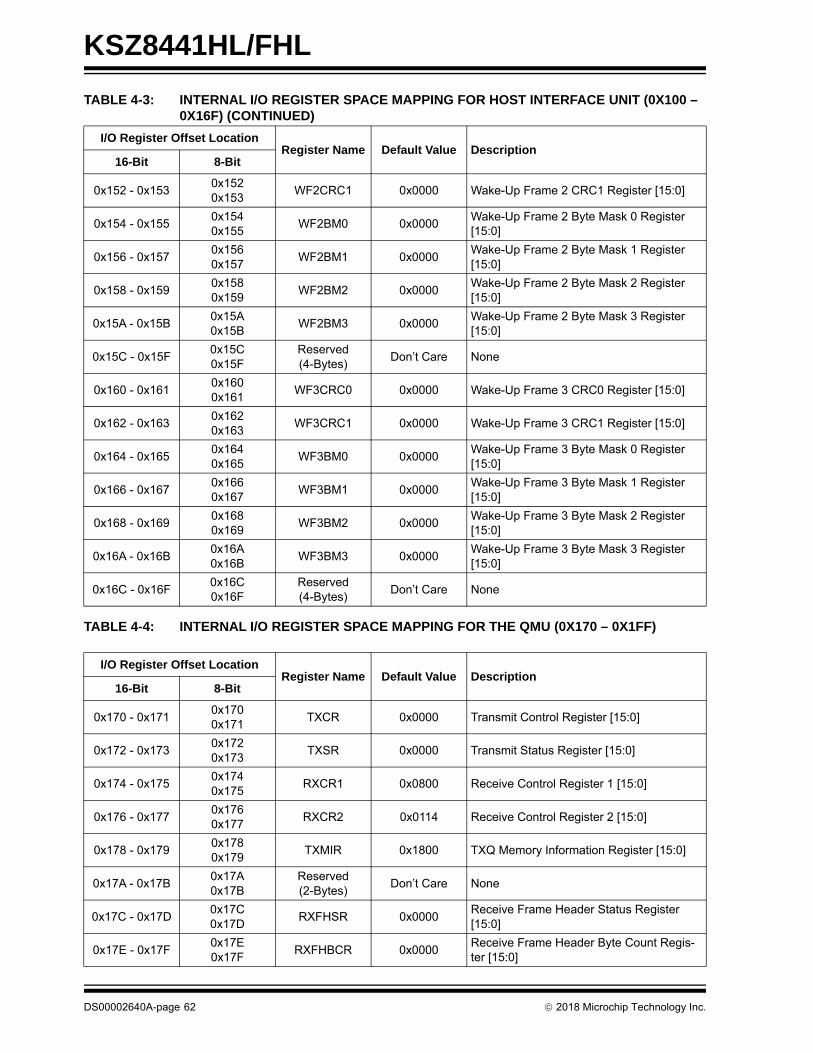
KSZ8441HL/FHL
0x152 - 0x1530x1520x153
WF2CRC1 0x0000 Wake-Up Frame 2 CRC1 Register [15:0]
0x154 - 0x1550x1540x155
WF2BM0 0x0000Wake-Up Frame 2 Byte Mask 0 Register [15:0]
0x156 - 0x1570x1560x157
WF2BM1 0x0000Wake-Up Frame 2 Byte Mask 1 Register [15:0]
0x158 - 0x1590x1580x159
WF2BM2 0x0000Wake-Up Frame 2 Byte Mask 2 Register [15:0]
0x15A - 0x15B0x15A0x15B
WF2BM3 0x0000Wake-Up Frame 2 Byte Mask 3 Register [15:0]
0x15C - 0x15F0x15C0x15F
Reserved(4-Bytes)
Don’t Care None
0x160 - 0x1610x1600x161
WF3CRC0 0x0000 Wake-Up Frame 3 CRC0 Register [15:0]
0x162 - 0x1630x1620x163
WF3CRC1 0x0000 Wake-Up Frame 3 CRC1 Register [15:0]
0x164 - 0x1650x1640x165
WF3BM0 0x0000Wake-Up Frame 3 Byte Mask 0 Register [15:0]
0x166 - 0x1670x1660x167
WF3BM1 0x0000Wake-Up Frame 3 Byte Mask 1 Register [15:0]
0x168 - 0x1690x1680x169
WF3BM2 0x0000Wake-Up Frame 3 Byte Mask 2 Register [15:0]
0x16A - 0x16B0x16A0x16B
WF3BM3 0x0000Wake-Up Frame 3 Byte Mask 3 Register [15:0]
0x16C - 0x16F0x16C0x16F
Reserved(4-Bytes)
Don’t Care None
TABLE 4-4: INTERNAL I/O REGISTER SPACE MAPPING FOR THE QMU (0X170 – 0X1FF)
I/O Register Offset LocationRegister Name Default Value Description
16-Bit 8-Bit
0x170 - 0x1710x1700x171
TXCR 0x0000 Transmit Control Register [15:0]
0x172 - 0x1730x1720x173
TXSR 0x0000 Transmit Status Register [15:0]
0x174 - 0x1750x1740x175
RXCR1 0x0800 Receive Control Register 1 [15:0]
0x176 - 0x1770x1760x177
RXCR2 0x0114 Receive Control Register 2 [15:0]
0x178 - 0x1790x1780x179
TXMIR 0x1800 TXQ Memory Information Register [15:0]
0x17A - 0x17B0x17A0x17B
Reserved(2-Bytes)
Don’t Care None
0x17C - 0x17D0x17C0x17D
RXFHSR 0x0000Receive Frame Header Status Register [15:0]
0x17E - 0x17F0x17E0x17F
RXFHBCR 0x0000Receive Frame Header Byte Count Regis-ter [15:0]
TABLE 4-3: INTERNAL I/O REGISTER SPACE MAPPING FOR HOST INTERFACE UNIT (0X100 – 0X16F) (CONTINUED)
I/O Register Offset LocationRegister Name Default Value Description
16-Bit 8-Bit
DS00002640A-page 62 2018 Microchip Technology Inc.

KSZ8441HL/FHL
0x180 - 0x1810x1800x181
TXQCR 0x0000 TXQ Command Register [15:0]
0x182 - 0x1830x1820x183
RXQCR 0x0000 RXQ Command Register [15:0]
0x184 - 0x1850x1840x185
TXFDPR 0x0000 TX Frame Data Pointer Register [15:0]
0x186 - 0x1870x1860x187
RXFDPR 0x1000 RX Frame Data Pointer Register [15:0]
0x188 - 0x18B0x1880x18B
Reserved(4-Bytes)
Don’t Care None
0x18C - 0x18D0x18C0x18D
RXDTTR 0x0000RX Duration Timer Threshold Register [15:0]
0x18E - 0x18F0x18E0x18F
RXDBCTR 0x0000RX Data Byte Count Threshold Register [15:0]
0x190 - 0x1910x1900x191
IER 0x0000 Interrupt Enable Register [15:0]
0x192 - 0x1930x1920x193
ISR 0x0000 Interrupt Status Register [15:0]
0x194 - 0x19B0x1940x19B
Reserved(8-Bytes)
Don’t Care None
0x19C - 0x19D0x19C0x19D
RXFCTR 0x0000RX Frame Count Threshold Register [7:0], [15:8] are Reserved
0x19E - 0x19F0x19E0x19F
TXNTFSR 0x0000 TX Next Total Frames Size Register [15:0]
0x1A0 - 0x1A10x1A00x1A1
MAHTR0 0x0000 MAC Address Hash Table Register 0 [15:0]
0x1A2 - 0x1A30x1A20x1A3
MAHTR1 0x0000 MAC Address Hash Table Register 1 [15:0]
0x1A4 - 0x1A50x1A40x1A5
MAHTR2 0x0000 MAC Address Hash Table Register 2 [15:0]
0x1A6 - 0x1A70x1A60x1A7
MAHTR3 0x0000 MAC Address Hash Table Register 3 [15:0]
0x1A8 - 0x1AF0x1A80x1AF
Reserved(8-Bytes)
Don’t Care None
0x1B0 - 0x1B10x1B00x1B1
FCLWR 0x0600Flow Control Low Water Mark Register [15:0]
0x1B2 - 0x1B30x1B20x1B3
FCHWR 0x0400Flow Control High Water Mark Register [15:0]
0x1B4 - 0x1B50x1B40x1B5
FCOWR 0x0040Flow Control Overrun Water Mark Register [15:0]
0x1B6 - 0x1B70x1B60x1B7
Reserved(2-Bytes)
Don’t Care None
0x1B8 - 0x1B90x1B80x1B9
RXFC 0x00 RX Frame Count[15:8], Reserved [7:0]
0x1BA - 0x1FF0x1BA0x1FF
Reserved(70-Bytes)
Don’t Care None
TABLE 4-4: INTERNAL I/O REGISTER SPACE MAPPING FOR THE QMU (0X170 – 0X1FF) (CONTINUED)
I/O Register Offset LocationRegister Name Default Value Description
16-Bit 8-Bit
2018 Microchip Technology Inc. DS00002640A-page 63

KSZ8441HL/FHL
TABLE 4-5: INTERNAL I/O REGISTER SPACE MAPPING FOR PTP TRIGGER OUTPUT (12 UNITS, 0X200 – 0X3FF)
I/O Register Offset LocationRegister Name Default Value Description
16-Bit 8-Bit
0x200 – 0x2010x2000x201
TRIG_ERR 0x0000 Trigger Output Unit Error Register [11:0]
0x202 – 0x2030x2020x203
TRIG_ACTIVE 0x0000 Trigger Output Unit Active Register [11:0]
0x204 – 0x2050x2040x205
TRIG_DONE 0x0000 Trigger Output Unit Done Register [11:0]
0x206 – 0x2070x2060x207
TRIG_EN 0x0000 Trigger Output Unit Enable Register [11:0]
0x208 – 0x2090x2080x209
TRIG_SW_RST 0x0000Trigger Output Unit Software Reset Regis-ter [11:0]
0x20A – 0x20B0x20A0x20B
TRIG12_PPS_WIDTH
0x0000Trigger Output Unit 12 PPS Pulse Width Register
0x20C – 0x21F0x20C0x21F
Reserved(20-Bytes)
Don’t Care None
0x220 – 0x2210x2200x221
TRIG1_T-GT_NSL
0x0000Trigger Output Unit 1 Target Time in Nano-seconds Low-Word Register [15:0]
0x222 – 0x2230x2220x223
TRIG1_T-GT_NSH
0x0000Trigger Output Unit 1 Target Time in Nano-seconds High-Word Register [29:16]
0x224 – 0x2250x2240x225
TRIG1_TGT_SL 0x0000Trigger Output Unit 1 Target Time in Sec-onds Low-Word Register [15:0]
0x226 – 0x2270x2260x227
TRIG1_T-GT_SH
0x0000Trigger Output Unit 1 Target Time in Sec-onds High-Word Register [31:16]
0x228 – 0x2290x2280x229
TRIG1_CFG_1 0x3C00Trigger Output Unit 1 Configuration/Control Register1
0x22A – 0x22B0x22A0x22B
TRIG1_CFG_2 0x0000Trigger Output Unit 1 Configuration/Control Register2
0x22C – 0x22D0x22C0x22D
TRIG1_CFG_3 0x0000Trigger Output Unit 1 Configuration/Control Register3
0x22E – 0x22F0x22E0x22F
TRIG1_CFG_4 0x0000Trigger Output Unit 1 Configuration/Control Register4
0x230 – 0x2310x2300x231
TRIG1_CFG_5 0x0000Trigger Output Unit 1 Configuration/Control Register5
0x232 – 0x2330x2320x233
TRIG1_CFG_6 0x0000Trigger Output Unit 1 Configuration/Control Register6
0x234 – 0x2350x2340x235
TRIG1_CFG_7 0x0000Trigger Output Unit 1 Configuration/Control Register7
0x236 – 0x2370x2360x237
TRIG1_CFG_8 0x0000Trigger Output Unit 1 Configuration/Control Register8
0x238 – 0x23F0x2380x23F
Reserved(8-Bytes)
Don’t Care None
0x240 – 0x2410x2400x241
TRIG2_T-GT_NSL
0x0000Trigger Output Unit 2 Target Time in Nano-seconds Low-Word Register [15:0]
0x242 – 0x2430x2420x243
TRIG2_T-GT_NSH
0x0000Trigger Output Unit 2 Target Time in Nano-seconds High-Word Register [29:16]
0x244 – 0x2450x2440x245
TRIG2_TGT_SL 0x0000Trigger Output Unit 2 Target Time in Sec-onds Low-Word Register [15:0]
DS00002640A-page 64 2018 Microchip Technology Inc.

KSZ8441HL/FHL
0x246 – 0x2470x2460x247
TRIG2_T-GT_SH
0x0000Trigger Output Unit 2 Target Time in Sec-onds High-Word Register [31:16]
0x248 – 0x2490x2480x249
TRIG2_CFG_1 0x3C00Trigger Output Unit 2 Configuration/Control Register1
0x24A – 0x24B0x24A0x24B
TRIG2_CFG_2 0x0000Trigger Output Unit 2 Configuration/Control Register2
0x24C – 0x24D0x24C0x24D
TRIG2_CFG_3 0x0000Trigger Output Unit 2 Configuration/Control Register3
0x24E – 0x24F0x24E0x24F
TRIG2_CFG_4 0x0000Trigger Output Unit 2 Configuration/Control Register4
0x250 – 0x2510x2500x251
TRIG2_CFG_5 0x0000Trigger Output Unit 2 Configuration/Control Register5
0x252 – 0x2530x2520x253
TRIG2_CFG_6 0x0000Trigger Output Unit 2 Configuration/Control Register6
0x254 – 0x2550x2540x255
TRIG2_CFG_7 0x0000Trigger Output Unit 2 Configuration/Control Register7
0x256 – 0x2570x2560x257
TRIG2_CFG_8 0x0000Trigger Output Unit 2 Configuration/Control Register8
0x258 – 0x25F0x2580x25F
Reserved(8-Bytes)
Don’t Care None
0x260 – 0x2610x2600x261
TRIG3_T-GT_NSL
0x0000Trigger Output Unit 3 Target Time in Nano-seconds Low-Word Register [15:0]
0x262 – 0x2630x2620x263
TRIG3_T-GT_NSH
0x0000Trigger Output Unit 3 Target Time in Nano-seconds High-Word Register [29:16]
0x264 – 0x2650x2640x265
TRIG3_TGT_SL 0x0000Trigger Output Unit 3 Target Time in Sec-onds Low-Word Register [15:0]
0x266 – 0x2670x2660x267
TRIG3_T-GT_SH
0x0000Trigger Output Unit 3 Target Time in Sec-onds High-Word Register [31:16]
0x268 – 0x2690x2680x269
TRIG3_CFG_1 0x3C00Trigger Output Unit 3 Configuration/Control Register1
0x26A – 0x26B0x26A0x26B
TRIG3_CFG_2 0x0000Trigger Output Unit 3 Configuration/Control Register2
0x26C – 0x26D0x26C0x26D
TRIG3_CFG_3 0x0000Trigger Output Unit 3 Configuration/Control Register3
0x26E – 0x26F0x26E0x26F
TRIG3_CFG_4 0x0000Trigger Output Unit 3 Configuration/Control Register4
0x270 – 0x2710x2700x271
TRIG3_CFG_5 0x0000Trigger Output Unit 3 Configuration/Control Register5
0x272 – 0x2730x2720x273
TRIG3_CFG_6 0x0000Trigger Output Unit 3 Configuration/Control Register6
0x274 – 0x2750x2740x275
TRIG3_CFG_7 0x0000Trigger Output Unit 3 Configuration/Control Register7
0x276 – 0x2770x2760x277
TRIG3_CFG_8 0x0000Trigger Output Unit 3 Configuration/Control Register8
0x278 – 0x27F0x2780x27F
Reserved(8-Bytes)
Don’t Care None
TABLE 4-5: INTERNAL I/O REGISTER SPACE MAPPING FOR PTP TRIGGER OUTPUT (12 UNITS, 0X200 – 0X3FF) (CONTINUED)
I/O Register Offset LocationRegister Name Default Value Description
16-Bit 8-Bit
2018 Microchip Technology Inc. DS00002640A-page 65

KSZ8441HL/FHL
0x280 – 0x2810x2800x281
TRIG4_T-GT_NSL
0x0000Trigger Output Unit 4 Target Time in Nano-seconds Low-Word Register [15:0]
0x282 – 0x2830x2820x283
TRIG4_T-GT_NSH
0x0000Trigger Output Unit 4 Target Time in Nano-seconds High-Word Register [29:16]
0x284 – 0x2850x2840x285
TRIG4_TGT_SL 0x0000Trigger Output Unit 4 Target Time in Sec-onds Low-Word Register [15:0]
0x286 – 0x2870x2860x287
TRIG4_T-GT_SH
0x0000Trigger Output Unit 4 Target Time in Sec-onds High-Word Register [31:16]
0x288 – 0x2890x2880x289
TRIG4_CFG_1 0x3C00Trigger Output Unit 4 Configuration/Control Register1
0x28A – 0x28B0x28A0x28B
TRIG4_CFG_2 0x0000Trigger Output Unit 4 Configuration/Control Register2
0x28C – 0x28D0x28C0x28D
TRIG4_CFG_3 0x0000Trigger Output Unit 4 Configuration/Control Register3
0x28E – 0x28F0x28E0x28F
TRIG4_CFG_4 0x0000Trigger Output Unit 4 Configuration/Control Register4
0x290 – 0x2910x2900x291
TRIG4_CFG_5 0x0000Trigger Output Unit 4 Configuration/Control Register5
0x292 – 0x2930x2920x293
TRIG4_CFG_6 0x0000Trigger Output Unit 4 Configuration/Control Register6
0x294 – 0x2950x2940x295
TRIG4_CFG_7 0x0000Trigger Output Unit 4 Configuration/Control Register7
0x296 – 0x2970x2960x297
TRIG4_CFG_8 0x0000Trigger Output Unit 4 Configuration/Control Register8
0x298 – 0x29F0x2980x29F
Reserved(8-Bytes)
Don’t Care None
0x2A0 – 0x2A10x2A00x2A1
TRIG5_T-GT_NSL
0x0000Trigger Output Unit 5 Target Time in Nano-seconds Low-Word Register [15:0]
0x2A2 – 0x2A30x2A20x2A3
TRIG5_T-GT_NSH
0x0000Trigger Output Unit 5 Target Time in Nano-seconds High-Word Register [29:16]
0x2A4 – 0x2A50x2A40x2A5
TRIG5_TGT_SL 0x0000Trigger Output Unit 5 Target Time in Sec-onds Low-Word Register [15:0]
0x2A6 – 0x2A70x2A60x2A7
TRIG5_T-GT_SH
0x0000Trigger Output Unit 5 Target Time in Sec-onds High-Word Register [31:16]
0x2A8 – 0x2A90x2A80x2A9
TRIG5_CFG_1 0x3C00Trigger Output Unit 5 Configuration/Control Register1
0x2AA – 0x2AB0x2AA0x2AB
TRIG5_CFG_2 0x0000Trigger Output Unit 5 Configuration/Control Register2
0x2AC – 0x2AD0x2AC0x2AD
TRIG5_CFG_3 0x0000Trigger Output Unit 5 Configuration/Control Register3
0x2AE – 0x2AF0x2AE0x2AF
TRIG5_CFG_4 0x0000Trigger Output Unit 5 Configuration/Control Register4
0x2B0 – 0x2B10x2B00x2B1
TRIG5_CFG_5 0x0000Trigger Output Unit 5 Configuration/Control Register5
0x2B2 – 0x2B30x2B20x2B3
TRIG5_CFG_6 0x0000Trigger Output Unit 5 Configuration/Control Register6
TABLE 4-5: INTERNAL I/O REGISTER SPACE MAPPING FOR PTP TRIGGER OUTPUT (12 UNITS, 0X200 – 0X3FF) (CONTINUED)
I/O Register Offset LocationRegister Name Default Value Description
16-Bit 8-Bit
DS00002640A-page 66 2018 Microchip Technology Inc.

KSZ8441HL/FHL
0x2B4 – 0x2B50x2B40x2B5
TRIG5_CFG_7 0x0000Trigger Output Unit 5 Configuration/Control Register7
0x2B6 – 0x2B70x2B60x2B7
TRIG5_CFG_8 0x0000Trigger Output Unit 5 Configuration/Control Register8
0x2B8 – 0x2BF0x2B80x2BF
Reserved(8-Bytes)
Don’t Care None
0x2C0 – 0x2C10x2C00x2C1
TRIG6_T-GT_NSL
0x0000Trigger Output Unit 6 Target Time in Nano-seconds Low-Word Register [15:0]
0x2C2 – 0x2C30x2C20x2C3
TRIG6_T-GT_NSH
0x0000Trigger Output Unit 6 Target Time in Nano-seconds High-Word Register [29:16]
0x2C4 – 0x2C50x2C40x2C5
TRIG6_TGT_SL 0x0000Trigger Output Unit 6 Target Time in Sec-onds Low-Word Register [15:0]
0x2C6 – 0x2C70x2C60x2C7
TRIG6_T-GT_SH
0x0000Trigger Output Unit 6 Target Time in Sec-onds High-Word Register [31:16]
0x2C8 – 0x2C90x2C80x2C9
TRIG6_CFG_1 0x3C00Trigger Output Unit 6 Configuration/Control Register1
0x2CA – 0x2CB0x2CA0x2CB
TRIG6_CFG_2 0x0000Trigger Output Unit 6 Configuration/Control Register2
0x2CC – 0x2CD0x2CC0x2CD
TRIG6_CFG_3 0x0000Trigger Output Unit 6 Configuration/Control Register3
0x2CE – 0x2CF0x2CE0x2CF
TRIG6_CFG_4 0x0000Trigger Output Unit 6 Configuration/Control Register4
0x2D0 – 0x2D10x2D00x2D1
TRIG6_CFG_5 0x0000Trigger Output Unit 6 Configuration/Control Register5
0x2D2 – 0x2D30x2D20x2D3
TRIG6_CFG_6 0x0000Trigger Output Unit 6 Configuration/Control Register6
0x2D4 – 0x2D50x2D40x2D5
TRIG6_CFG_7 0x0000Trigger Output Unit 6 Configuration/Control Register7
0x2D6 – 0x2D70x2D60x2D7
TRIG6_CFG_8 0x0000Trigger Output Unit 6 Configuration/Control Register8
0x2D8 – 0x2DF0x2D80x2DF
Reserved(8-Bytes)
Don’t Care None
0x2E0 – 0x2E10x2E00x2E1
TRIG7_T-GT_NSL
0x0000Trigger Output Unit 7 Target Time in Nano-seconds Low-Word Register [15:0]
0x2E2 – 0x2E30x2E20x2E3
TRIG7_T-GT_NSH
0x0000Trigger Output Unit 7 Target Time in Nano-seconds High-Word Register [29:16]
0x2E4 – 0x2E50x2E40x2E5
TRIG7_TGT_SL 0x0000Trigger Output Unit 7 Target Time in Sec-onds Low-Word Register [15:0]
0x2E6 – 0x2E70x2E60x2E7
TRIG7_T-GT_SH
0x0000Trigger Output Unit 7 Target Time in Sec-onds High-Word Register [31:16]
0x2E8 – 0x2E90x2E80x2E9
TRIG7_CFG_1 0x3C00Trigger Output Unit 7 Configuration/Control Register1
0x2EA – 0x2EB0x2EA0x2EB
TRIG7_CFG_2 0x0000Trigger Output Unit 7 Configuration/Control Register2
0x2EC – 0x2ED0x2EC0x2ED
TRIG7_CFG_3 0x0000Trigger Output Unit 7 Configuration/Control Register3
TABLE 4-5: INTERNAL I/O REGISTER SPACE MAPPING FOR PTP TRIGGER OUTPUT (12 UNITS, 0X200 – 0X3FF) (CONTINUED)
I/O Register Offset LocationRegister Name Default Value Description
16-Bit 8-Bit
2018 Microchip Technology Inc. DS00002640A-page 67
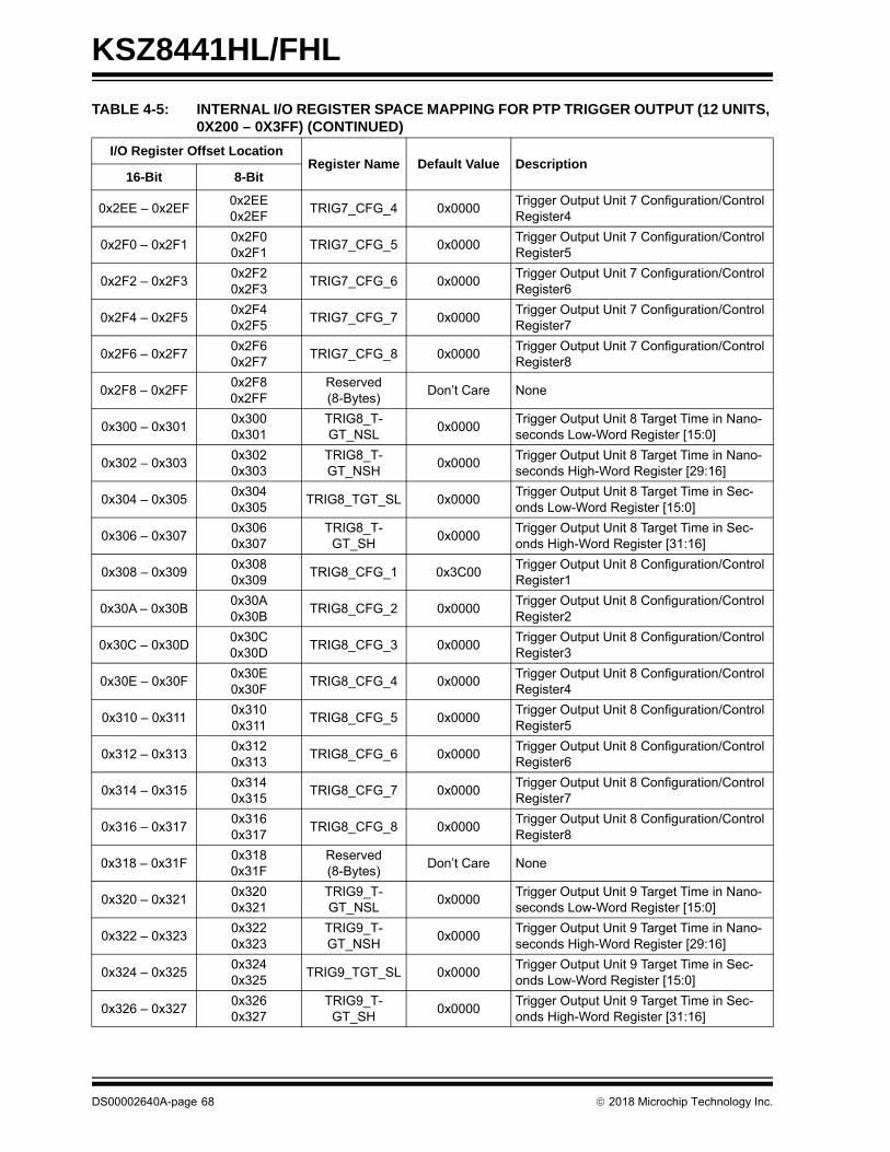
KSZ8441HL/FHL
0x2EE – 0x2EF0x2EE0x2EF
TRIG7_CFG_4 0x0000Trigger Output Unit 7 Configuration/Control Register4
0x2F0 – 0x2F10x2F00x2F1
TRIG7_CFG_5 0x0000Trigger Output Unit 7 Configuration/Control Register5
0x2F2 – 0x2F30x2F20x2F3
TRIG7_CFG_6 0x0000Trigger Output Unit 7 Configuration/Control Register6
0x2F4 – 0x2F50x2F40x2F5
TRIG7_CFG_7 0x0000Trigger Output Unit 7 Configuration/Control Register7
0x2F6 – 0x2F70x2F60x2F7
TRIG7_CFG_8 0x0000Trigger Output Unit 7 Configuration/Control Register8
0x2F8 – 0x2FF0x2F80x2FF
Reserved(8-Bytes)
Don’t Care None
0x300 – 0x3010x3000x301
TRIG8_T-GT_NSL
0x0000Trigger Output Unit 8 Target Time in Nano-seconds Low-Word Register [15:0]
0x302 – 0x3030x3020x303
TRIG8_T-GT_NSH
0x0000Trigger Output Unit 8 Target Time in Nano-seconds High-Word Register [29:16]
0x304 – 0x3050x3040x305
TRIG8_TGT_SL 0x0000Trigger Output Unit 8 Target Time in Sec-onds Low-Word Register [15:0]
0x306 – 0x3070x3060x307
TRIG8_T-GT_SH
0x0000Trigger Output Unit 8 Target Time in Sec-onds High-Word Register [31:16]
0x308 – 0x3090x3080x309
TRIG8_CFG_1 0x3C00Trigger Output Unit 8 Configuration/Control Register1
0x30A – 0x30B0x30A0x30B
TRIG8_CFG_2 0x0000Trigger Output Unit 8 Configuration/Control Register2
0x30C – 0x30D0x30C0x30D
TRIG8_CFG_3 0x0000Trigger Output Unit 8 Configuration/Control Register3
0x30E – 0x30F0x30E0x30F
TRIG8_CFG_4 0x0000Trigger Output Unit 8 Configuration/Control Register4
0x310 – 0x3110x3100x311
TRIG8_CFG_5 0x0000Trigger Output Unit 8 Configuration/Control Register5
0x312 – 0x3130x3120x313
TRIG8_CFG_6 0x0000Trigger Output Unit 8 Configuration/Control Register6
0x314 – 0x3150x3140x315
TRIG8_CFG_7 0x0000Trigger Output Unit 8 Configuration/Control Register7
0x316 – 0x3170x3160x317
TRIG8_CFG_8 0x0000Trigger Output Unit 8 Configuration/Control Register8
0x318 – 0x31F0x3180x31F
Reserved(8-Bytes)
Don’t Care None
0x320 – 0x3210x3200x321
TRIG9_T-GT_NSL
0x0000Trigger Output Unit 9 Target Time in Nano-seconds Low-Word Register [15:0]
0x322 – 0x3230x3220x323
TRIG9_T-GT_NSH
0x0000Trigger Output Unit 9 Target Time in Nano-seconds High-Word Register [29:16]
0x324 – 0x3250x3240x325
TRIG9_TGT_SL 0x0000Trigger Output Unit 9 Target Time in Sec-onds Low-Word Register [15:0]
0x326 – 0x3270x3260x327
TRIG9_T-GT_SH
0x0000Trigger Output Unit 9 Target Time in Sec-onds High-Word Register [31:16]
TABLE 4-5: INTERNAL I/O REGISTER SPACE MAPPING FOR PTP TRIGGER OUTPUT (12 UNITS, 0X200 – 0X3FF) (CONTINUED)
I/O Register Offset LocationRegister Name Default Value Description
16-Bit 8-Bit
DS00002640A-page 68 2018 Microchip Technology Inc.

KSZ8441HL/FHL
0x328 – 0x3290x3280x329
TRIG9_CFG_1 0x3C00Trigger Output Unit 9 Configuration/Control Register1
0x32A – 0x32B0x32A0x32B
TRIG9_CFG_2 0x0000Trigger Output Unit 9 Configuration/Control Register2
0x32C – 0x32D0x32C0x32D
TRIG9_CFG_3 0x0000Trigger Output Unit 9 Configuration/Control Register3
0x32E – 0x32F0x32E0x32F
TRIG9_CFG_4 0x0000Trigger Output Unit 9 Configuration/Control Register4
0x330 – 0x3310x3300x331
TRIG9_CFG_5 0x0000Trigger Output Unit 9 Configuration/Control Register5
0x332 – 0x3330x3320x333
TRIG9_CFG_6 0x0000Trigger Output Unit 9 Configuration/Control Register6
0x334 – 0x3350x3340x335
TRIG9_CFG_7 0x0000Trigger Output Unit 9 Configuration/Control Register7
0x336 – 0x3370x3360x337
TRIG9_CFG_8 0x0000Trigger Output Unit 9 Configuration/Control Register8
0x338 – 0x33F0x3380x33F
Reserved(8-Bytes)
Don’t Care None
0x340 – 0x3410x3400x341
TRIG10_T-GT_NSL
0x0000Trigger Output Unit 10 Target Time in Nano-seconds Low-Word Register [15:0]
0x342 – 0x3430x3420x343
TRIG10_T-GT_NSH
0x0000Trigger Output Unit 10 Target Time in Nano-seconds High-Word Register [29:16]
0x344 – 0x3450x3440x345
TRIG10_T-GT_SL
0x0000Trigger Output Unit 10 Target Time in Sec-onds Low-Word Register [15:0]
0x346 – 0x3470x3460x347
TRIG10_T-GT_SH
0x0000Trigger Output Unit 10 Target Time in Sec-onds High-Word Register [31:16]
0x348 – 0x3490x3480x349
TRIG10_CFG_1 0x3C00Trigger Output Unit 10 Configuration/Con-trol Register1
0x34A – 0x34B0x34A0x34B
TRIG10_CFG_2 0x0000Trigger Output Unit 10 Configuration/Con-trol Register2
0x34C – 0x34D0x34C0x34D
TRIG10_CFG_3 0x0000Trigger Output Unit 10 Configuration/Con-trol Register3
0x34E – 0x34F0x34E0x34F
TRIG10_CFG_4 0x0000Trigger Output Unit 10 Configuration/Con-trol Register4
0x350 – 0x3510x3500x351
TRIG10_CFG_5 0x0000Trigger Output Unit 10 Configuration/Con-trol Register5
0x352 – 0x3530x3520x353
TRIG10_CFG_6 0x0000Trigger Output Unit 10 Configuration/Con-trol Register6
0x354 – 0x3550x3540x355
TRIG10_CFG_7 0x0000Trigger Output Unit 10 Configuration/Con-trol Register7
0x356 – 0x3570x3560x357
TRIG10_CFG_8 0x0000Trigger Output Unit 10 Configuration/Con-trol Register8
0x358 – 0x35F0x3580x35F
Reserved(8-Bytes)
Don’t Care None
0x360 – 0x3610x3600x361
TRIG11_T-GT_NSL
0x0000Trigger Output Unit 11 Target Time in Nano-seconds Low-Word Register [15:0]
TABLE 4-5: INTERNAL I/O REGISTER SPACE MAPPING FOR PTP TRIGGER OUTPUT (12 UNITS, 0X200 – 0X3FF) (CONTINUED)
I/O Register Offset LocationRegister Name Default Value Description
16-Bit 8-Bit
2018 Microchip Technology Inc. DS00002640A-page 69

KSZ8441HL/FHL
0x362 – 0x3630x3620x363
TRIG11_T-GT_NSH
0x0000Trigger Output Unit 11 Target Time in Nano-seconds High-Word Register [29:16]
0x364 – 0x3650x3640x365
TRIG11_T-GT_SL
0x0000Trigger Output Unit 11 Target Time in Sec-onds Low-Word Register [15:0]
0x366 – 0x3670x3660x367
TRIG11_T-GT_SH
0x0000Trigger Output Unit 11 Target Time in Sec-onds High-Word Register [31:16]
0x368 – 0x3690x3680x369
TRIG11_CFG_1 0x3C00Trigger Output Unit 11 Configuration/Con-trol Register1
0x36A – 0x36B0x36A0x36B
TRIG11_CFG_2 0x0000Trigger Output Unit 11 Configuration/Con-trol Register2
0x36C – 0x36D0x36C0x36D
TRIG11_CFG_3 0x0000Trigger Output Unit 11 Configuration/Con-trol Register3
0x36E – 0x36F0x36E0x36F
TRIG11_CFG_4 0x0000Trigger Output Unit 11 Configuration/Con-trol Register4
0x370 – 0x3710x3700x371
TRIG11_CFG_5 0x0000Trigger Output Unit 11 Configuration/Con-trol Register5
0x372 – 0x3730x3720x373
TRIG11_CFG_6 0x0000Trigger Output Unit 11 Configuration/Con-trol Register6
0x374 – 0x3750x3740x375
TRIG11_CFG_7 0x0000Trigger Output Unit 11 Configuration/Con-trol Register7
0x376 – 0x3770x3760x377
TRIG11_CFG_8 0x0000Trigger Output Unit 11 Configuration/Con-trol Register8
0x378 – 0x37F0x3780x37F
Reserved(8-Bytes)
Don’t Care None
0x380 – 0x3810x3800x381
TRIG12_T-GT_NSL
0x0000Trigger Output Unit 12 Target Time in Nano-seconds Low-Word Register [15:0]
0x382 – 0x3830x3820x383
TRIG12_T-GT_NSH
0x0000Trigger Output Unit 12 Target Time in Nano-seconds High-Word Register [29:16]
0x384 – 0x3850x3840x385
TRIG12_T-GT_SL
0x0000Trigger Output Unit 12 Target Time in Sec-onds Low-Word Register [15:0]
0x386 – 0x3870x3860x387
TRIG12_T-GT_SH
0x0000Trigger Output Unit 12 Target Time in Sec-onds High-Word Register [31:16]
0x388 – 0x3890x3880x389
TRIG12_CFG_1 0x3C00Trigger Output Unit 12 Configuration/Con-trol Register1
0x38A – 0x38B0x38A0x38B
TRIG12_CFG_2 0x0000Trigger Output Unit 12 Configuration/Con-trol Register2
0x38C – 0x38D0x38C0x38D
TRIG12_CFG_3 0x0000Trigger Output Unit 12 Configuration/Con-trol Register3
0x38E – 0x38F0x38E0x38F
TRIG12_CFG_4 0x0000Trigger Output Unit 12 Configuration/Con-trol Register4
0x390 – 0x3910x3900x391
TRIG12_CFG_5 0x0000Trigger Output Unit 12 Configuration/Con-trol Register5
0x392 – 0x3930x3920x393
TRIG12_CFG_6 0x0000Trigger Output Unit 12 Configuration/Con-trol Register6
0x394 – 0x3950x3940x395
TRIG12_CFG_7 0x0000Trigger Output Unit 12 Configuration/Con-trol Register7
TABLE 4-5: INTERNAL I/O REGISTER SPACE MAPPING FOR PTP TRIGGER OUTPUT (12 UNITS, 0X200 – 0X3FF) (CONTINUED)
I/O Register Offset LocationRegister Name Default Value Description
16-Bit 8-Bit
DS00002640A-page 70 2018 Microchip Technology Inc.

KSZ8441HL/FHL
0x396 – 0x3970x3960x397
TRIG12_CFG_8 0x0000Trigger Output Unit 12 Configuration/Con-trol Register8
0x398 – 0x3FF0x3980x3FF
Reserved(104-Bytes)
Don’t Care None
TABLE 4-6: INTERNAL I/O REGISTER SPACE MAPPING FOR PTP EVENT TIME STAMP INPUTS (12 UNITS, 0X400 – 0X5FF)
I/O Register Offset LocationRegister Name Default Value Description
16-Bit 8-Bit
0x400 – 0x4010x4000x401
TS_RDY 0x0000 Input Unit Ready Register [11:0]
0x402 – 0x4030x4020x403
TS_EN 0x0000Time stamp Input Unit Enable Register [11:0]
0x404 – 0x4050x4040x405
TS_SW_RST 0x0000Time stamp Input Unit Software Reset Reg-ister [11:0]
0x406 – 0x41F0x4060x41F
Reserved(26-Bytes)
Don’t Care None
0x420 – 0x4210x4200x421
TS1_STATUS 0x0000 Time stamp Input Unit 1 Status Register
0x422 – 0x4230x4220x423
TS1_CFG 0x0000Time stamp Input Unit 1 Configuration/Con-trol Register
0x424 – 0x4250x4240x425
TS1_SM-PL1_NSL
0x0000Time stamp Unit 1 Input Sample Time (1st) in Nanoseconds Low-Word Register [15:0]
0x426 – 0x4270x4260x427
TS1_SM-PL1_NSH
0x0000Time stamp Unit 1 Input Sample Time (1st) in Nanoseconds High-Word Register [29:16]
0x428 – 0x4290x4280x429
TS1_SM-PL1_SL
0x0000Time stamp Unit 1 Input Sample Time (1st) in Seconds Low-Word Register [15:0]
0x42A – 0x42B0x42A0x42B
TS1_SM-PL1_SH
0x0000Time stamp Unit 1 Input Sample Time (1st) in Seconds High-Word Register [31:16]
0x42C – 0x42D0x42C0x42D
TS1_SMPL1_-SUB_NS
0x0000Time stamp Unit 1 Input Sample Time (1st) in Sub-Nanoseconds Register [2:0]
0x42E – 0x4330x42E0x433
Reserved(6-Bytes)
Don’t Care None
0x434 – 0x4350x4340x435
TS1_SM-PL2_NSL
0x0000Time stamp Unit 1 Input Sample Time (2nd) in Nanoseconds Low-Word Register [15:0]
0x436 – 0x4370x4360x437
TS1_SM-PL2_NSH
0x0000Time stamp Unit 1 Input Sample Time (2nd) in Nanoseconds High-Word Register [29:16]
0x438 – 0x4390x4380x439
TS1_SM-PL2_SL
0x0000Time stamp Unit 1 Input Sample Time (2nd) in Seconds Low-Word Register [15:0]
0x43A – 0x43B0x43A0x43B
TS1_SM-PL2_SH
0x0000Time stamp Unit 1 Input Sample Time (2nd) in Seconds High-Word Register [31:16]
0x43C – 0x43D0x43C0x43D
TS1_SMPL2_-SUB_NS
0x0000Time stamp Unit 1 Input Sample Time (2nd) in Sub-Nanoseconds Register [2:0]
0x43E – 0x43F0x43E0x43F
Reserved(2-Bytes)
Don’t Care None
TABLE 4-5: INTERNAL I/O REGISTER SPACE MAPPING FOR PTP TRIGGER OUTPUT (12 UNITS, 0X200 – 0X3FF) (CONTINUED)
I/O Register Offset LocationRegister Name Default Value Description
16-Bit 8-Bit
2018 Microchip Technology Inc. DS00002640A-page 71

KSZ8441HL/FHL
0x440 – 0x4410x4400x441
TS2_STATUS 0x0000 Time stamp Input Unit 2 Status Register
0x442 – 0x4430x4420x443
TS2_CFG 0x0000Time stamp Input Unit 2 Configuration/Con-trol Register
0x444 – 0x4450x4440x445
TS2_SM-PL1_NSL
0x0000Time stamp Unit 2 Input Sample Time (1st) in Nanoseconds Low-Word Register [15:0]
0x446 – 0x4470x4460x447
TS2_SM-PL1_NSH
0x0000Time stamp Unit 2 Input Sample Time (1st) in Nanoseconds High-Word Register [29:16]
0x448 – 0x4490x4480x449
TS2_SM-PL1_SL
0x0000Time stamp Unit 2 Input Sample Time (1st) in Seconds Low-Word Register [15:0]
0x44A – 0x44B0x44A0x44B
TS2_SM-PL1_SH
0x0000Time stamp Unit 2 Input Sample Time (1st) in Seconds High-Word Register [31:16]
0x44C – 0x44D0x44C0x44D
TS2_SMPL1_-SUB_NS
0x0000Time stamp Unit 2 Input Sample Time (1st) in Sub-Nanoseconds Register [2:0]
0x44E – 0x4530x44E0x453
Reserved(6-Bytes)
Don’t Care None
0x454 – 0x4550x4540x455
TS2_SM-PL2_NSL
0x0000Time stamp Unit 2 Input Sample Time (2nd) in Nanoseconds Low-Word Register [15:0]
0x456 – 0x4570x4560x457
TS2_SM-PL2_NSH
0x0000Time stamp Unit 2 Input Sample Time (2nd) in Nanoseconds High-Word Register [29:16]
0x458 – 0x4590x4580x459
TS2_SMP2_SL 0x0000Time stamp Unit 2 Input Sample Time (2nd) in Seconds Low-Word Register [15:0]
0x45A – 0x45B0x45A0x45B
TS2_SM-PL2_SH
0x0000Time stamp Unit 2 Input Sample Time (2nd) in Seconds High-Word Register [31:16]
0x45C – 0x45D0x45C0x45D
TS2_SMPL2_-SUB_NS
0x0000Time stamp Unit 2 Input Sample Time (2nd) in Sub-Nanoseconds Register [2:0]
0x45E – 0x45F0x45E0x45F
Reserved(2-Bytes)
Don’t Care None
0x460 – 0x4610x4600x461
TS3_STATUS 0x0000 Time stamp Input Unit 3 Status Register
0x462 – 0x4630x4620x463
TS3_CFG 0x0000Time stamp Input Unit 3 Configuration/Con-trol Register
0x464 – 0x4650x4640x465
TS3_SM-PL1_NSL
0x0000Time stamp Unit 3 Input Sample Time (1st) in Nanoseconds Low-Word Register [15:0]
0x466 – 0x4670x4660x467
TS3_SM-PL1_NSH
0x0000Time stamp Unit 3 Input Sample Time (1st) in Nanoseconds High-Word Register [29:16]
0x468 – 0x4690x4680x469
TS3_SM-PL1_SL
0x0000Time stamp Unit 3 Input Sample Time (1st) in Seconds Low-Word Register [15:0]
0x46A – 0x46B0x46A0x46B
TS3_SM-PL1_SH
0x0000Time stamp Unit 3 Input Sample Time (1st) in Seconds High-Word Register [31:16]
0x46C – 0x46D0x46C0x46D
TS3_SMPL1_-SUB_NS
0x0000Time stamp Unit 3 Input Sample Time (1st) in Sub-Nanoseconds Register [2:0]
0x46E – 0x4730x46E0x473
Reserved(6-Bytes)
Don’t Care None
TABLE 4-6: INTERNAL I/O REGISTER SPACE MAPPING FOR PTP EVENT TIME STAMP INPUTS (12 UNITS, 0X400 – 0X5FF) (CONTINUED)
I/O Register Offset LocationRegister Name Default Value Description
16-Bit 8-Bit
DS00002640A-page 72 2018 Microchip Technology Inc.

KSZ8441HL/FHL
0x474 – 0x4750x4740x475
TS3_SM-PL2_NSL
0x0000Time stamp Unit 3 Input Sample Time (2nd) in Nanoseconds Low-Word Register [15:0]
0x476 – 0x4770x4760x477
TS3_SM-PL2_NSH
0x0000Time stamp Unit 3 Input Sample Time (2nd) in Nanoseconds High-Word Register [29:16]
0x478 – 0x4790x4780x479
TS3_SMP2_SL 0x0000Time stamp Unit 3 Input Sample Time (2nd) in Seconds Low-Word Register [15:0]
0x47A – 0x47B0x47A0x47B
TS3_SM-PL2_SH
0x0000Time stamp Unit 3 Input Sample Time (2nd) in Seconds High-Word Register [31:16]
0x47C – 0x47D0x47C0x47D
TS3_SMPL2_-SUB_NS
0x0000Time stamp Unit 3 Input Sample Time (2nd) in Sub-Nanoseconds Register [2:0]
0x47E – 0x47F0x47E0x47F
Reserved(2-Bytes)
Don’t Care None
0x480 – 0x4810x4800x481
TS4_STATUS 0x0000 Time stamp Input Unit 4 Status Register
0x482 – 0x4830x4820x483
TS4_CFG 0x0000Time stamp Input Unit 4 Configuration/Con-trol Register
0x484 – 0x4850x4840x485
TS4_SM-PL1_NSL
0x0000Time stamp Unit 4 Input Sample Time (1st) in Nanoseconds Low-Word Register [15:0]
0x486 – 0x4870x4860x487
TS4_SM-PL1_NSH
0x0000Time stamp Unit 4 Input Sample Time (1st) in Nanoseconds High-Word Register [29:16]
0x488 – 0x4890x4880x489
TS4_SM-PL1_SL
0x0000Time stamp Unit 4 Input Sample Time (1st) in Seconds Low-Word Register [15:0]
0x48A – 0x48B0x48A0x48B
TS4_SM-PL1_SH
0x0000Time stamp Unit 4 Input Sample Time (1st) in Seconds High-Word Register [31:16]
0x48C – 0x48D0x48C0x48D
TS4_SMPL1_-SUB_NS
0x0000Time stamp Unit 4 Input Sample Time (1st) in Sub-Nanoseconds Register [2:0]
0x48E – 0x4930x48E0x493
Reserved(6-Bytes)
Don’t Care None
0x494 – 0x4950x4940x495
TS4_SM-PL2_NSL
0x0000Time stamp Unit 4 Input Sample Time (2nd) in Nanoseconds Low-Word Register [15:0]
0x496 – 0x4970x4960x497
TS4_SM-PL2_NSH
0x0000Time stamp Unit 4 Input Sample Time (2nd) in Nanoseconds High-Word Register [29:16]
0x498 – 0x4990x4980x499
TS4_SMP2_SL 0x0000Time stamp Unit 4 Input Sample Time (2nd) in Seconds Low-Word Register [15:0]
0x49A – 0x49B0x49A0x49B
TS4_SM-PL2_SH
0x0000Time stamp Unit 4 Input Sample Time (2nd) in Seconds High-Word Register [31:16]
0x49C – 0x49D0x49C0x49D
TS4_SMPL2_-SUB_NS
0x0000Time stamp Unit 4 Input Sample Time (2nd) in Sub-Nanoseconds Register [2:0]
0x49E – 0x49F0x49E0x49F
Reserved(2-Bytes)
Don’t Care None
0x4A0 – 0x4A10x4A00x4A1
TS5_STATUS 0x0000 Time stamp Input Unit 5 Status Register
0x4A2 – 0x4A30x4A20x4A3
TS5_CFG 0x0000Time stamp Input Unit 5 Configuration/Con-trol Register
TABLE 4-6: INTERNAL I/O REGISTER SPACE MAPPING FOR PTP EVENT TIME STAMP INPUTS (12 UNITS, 0X400 – 0X5FF) (CONTINUED)
I/O Register Offset LocationRegister Name Default Value Description
16-Bit 8-Bit
2018 Microchip Technology Inc. DS00002640A-page 73

KSZ8441HL/FHL
0x4A4 – 0x4A50x4A4
0x4A5TS5_SMPL1_
NSL0x0000
Time stamp Unit 5 Input Sample Time (1st) in Nanoseconds Low-Word Register [15:0]
0x4A6 – 0x4A70x4A6
0x4A7TS5_SMPL1_
NSH0x0000
Time stamp Unit 5 Input Sample Time (1st) in Nanoseconds High-Word Register [29:16]
0x4A8 – 0x4A90x4A80x4A9
TS5_SM-PL1_SL
0x0000Time stamp Unit 5 Input Sample Time (1st) in Seconds Low-Word Register [15:0]
0x4AA – 0x4AB0x4AA0x4AB
TS5_SM-PL1_SH
0x0000Time stamp Unit 5 Input Sample Time (1st) in Seconds High-Word Register [31:16]
0x4AC – 0x4AD0x4AC0x4AD
TS5_SMPL1_-SUB_NS
0x0000Time stamp Unit 5 Input Sample Time (1st) in Sub-Nanoseconds Register [2:0]
0x4AE – 0x4B30x4AE0x4B3
Reserved(6-Bytes)
Don’t Care None
0x4B4 – 0x4B50x4B40x4B5
TS5_SM-PL2_NSL
0x0000Time stamp Unit 5 Input Sample Time (2nd) in Nanoseconds Low-Word Register [15:0]
0x4B6 – 0x4B70x4B60x4B7
TS5_SM-PL2_NSH
0x0000Time stamp Unit 5 Input Sample Time (2nd) in Nanoseconds High-Word Register [29:16]
0x4B8 – 0x4B90x4B80x4B9
TS5_SMP2_SL 0x0000Time stamp Unit 5 Input Sample Time (2nd) in Seconds Low-Word Register [15:0]
0x4BA – 0x4BB0x4BA0x4BB
TS5_SM-PL2_SH
0x0000Time stamp Unit 5 Input Sample Time (2nd) in Seconds High-Word Register [31:16]
0x4BC – 0x4BD0x4BC0x4BD
TS5_SMPL2_-SUB_NS
0x0000Time stamp Unit 5 Input Sample Time (2nd) in Sub-Nanoseconds Register [2:0]
0x4BE – 0x4BF0x4BE0x4BF
Reserved(2-Bytes)
Don’t Care None
0x4C0 – 0x4C10x4C00x4C1
TS6_STATUS 0x0000 Time stamp Input Unit 6 Status Register
0x4C2 – 0x4C30x4C20x4C3
TS6_CFG 0x0000Time stamp Input Unit 6 Configuration/Con-trol Register
0x4C4 – 0x4C50x4C40x4C5
TS6_SM-PL1_NSL
0x0000Time stamp Unit 6 Input Sample Time (1st) in Nanoseconds Low-Word Register [15:0]
0x4C6 – 0x4C70x4C60x4C7
TS6_SM-PL1_NSH
0x0000Time stamp Unit 6 Input Sample Time (1st) in Nanoseconds High-Word Register [29:16]
0x4C8 – 0x4C90x4C80x4C9
TS6_SM-PL1_SL
0x0000Time stamp Unit 6 Input Sample Time (1st) in Seconds Low-Word Register [15:0]
0x4CA – 0x4CB0x4CA0x4CB
TS6_SM-PL1_SH
0x0000Time stamp Unit 6 Input Sample Time (1st) in Seconds High-Word Register [31:16]
0x4CC – 0x4CD0x4CC0x4CD
TS6_SMPL1_-SUB_NS
0x0000Time stamp Unit 6 Input Sample Time (1st) in Sub-Nanoseconds Register [2:0]
0x4CE – 0x4D30x4CE0x4D3
Reserved(6-Bytes)
Don’t Care None
0x4D4 – 0x4D50x4D40x4D5
TS6_SM-PL2_NSL
0x0000Time stamp Unit 6 Input Sample Time (2nd) in Nanoseconds Low-Word Register [15:0]
TABLE 4-6: INTERNAL I/O REGISTER SPACE MAPPING FOR PTP EVENT TIME STAMP INPUTS (12 UNITS, 0X400 – 0X5FF) (CONTINUED)
I/O Register Offset LocationRegister Name Default Value Description
16-Bit 8-Bit
DS00002640A-page 74 2018 Microchip Technology Inc.

KSZ8441HL/FHL
0x4D6 – 0x4D70x4D60x4D7
TS6_SM-PL2_NSH
0x0000Time stamp Unit 6 Input Sample Time (2nd) in Nanoseconds High-Word Register [29:16]
0x4D8 – 0x4D90x4D80x4D9
TS6_SMP2_SL 0x0000Time stamp Unit 6 Input Sample Time (2nd) in Seconds Low-Word Register [15:0]
0x4DA – 0x4DB0x4DA0x4DB
TS6_SM-PL2_SH
0x0000Time stamp Unit 6 Input Sample Time (2nd) in Seconds High-Word Register [31:16]
0x4DC – 0x4DD0x4DC0x4DD
TS6_SMPL2_-SUB_NS
0x0000Time stamp Unit 6 Input Sample Time (2nd) in Sub-Nanoseconds Register [2:0]
0x4DE – 0x4DF0x4DE0x4DF
Reserved(2-Bytes)
Don’t Care None
0x4E0 – 0x4E10x4E00x4E1
TS7_STATUS 0x0000 Time stamp Input Unit 7 Status Register
0x4E2 – 0x4E30x4E20x4E3
TS7_CFG 0x0000Time stamp Input Unit 7 Configuration/Con-trol Register
0x4E4 – 0x4E50x4E40x4E5
TS7_SM-PL1_NSL
0x0000Time stamp Unit 7 Input Sample Time (1st) in Nanoseconds Low-Word Register [15:0]
0x4E6 – 0x4E70x4E60x4E7
TS7_SM-PL1_NSH
0x0000Time stamp Unit 7 Input Sample Time (1st) in Nanoseconds High-Word Register [29:16]
0x4E8 – 0x4E90x4E80x4E9
TS7_SM-PL1_SL
0x0000Time stamp Unit 7 Input Sample Time (1st) in Seconds Low-Word Register [15:0]
0x4EA – 0x4EB0x4EA0x4EB
TS7_SM-PL1_SH
0x0000Time stamp Unit 7 Input Sample Time (1st) in Seconds High-Word Register [31:16]
0x4EC – 0x4ED0x4EC0x4ED
TS7_SMPL1_-SUB_NS
0x0000Time stamp Unit 7 Input Sample Time (1st) in Sub-Nanoseconds Register [2:0]
0x4EE – 0x4F30x4EE0x4F3
Reserved(6-Bytes)
Don’t Care None
0x4F4 – 0x4F50x4F40x4F5
TS7_SM-PL2_NSL
0x0000Time stamp Unit 7 Input Sample Time (2nd) in Nanoseconds Low-Word Register [15:0]
0x4F6 – 0x4F70x4F60x4F7
TS7_SM-PL2_NSH
0x0000Time stamp Unit 7 Input Sample Time (2nd) in Nanoseconds High-Word Register [29:16]
0x4F8 – 0x4F90x4F80x4F9
TS7_SMP2_SL 0x0000Time stamp Unit 7 Input Sample Time (2nd) in Seconds Low-Word Register [15:0]
0x4FA – 0x4FB0x4FA0x4FB
TS7_SM-PL2_SH
0x0000Time stamp Unit 7 Input Sample Time (2nd) in Seconds High-Word Register [31:16]
0x4FC – 0x4FD0x4FC0x4FD
TS7_SMPL2_-SUB_NS
0x0000Time stamp Unit 7 Input Sample Time (2nd) in Sub-Nanoseconds Register [2:0]
0x4FE – 0x4FF0x4FE0x4FF
Reserved(2-Bytes)
Don’t Care None
0x500 – 0x5010x5000x501
TS8_STATUS 0x0000 Time stamp Input Unit 8 Status Register
0x502 – 0x5030x5020x503
TS8_CFG 0x0000Time stamp Input Unit 8 Configuration/Con-trol Register
0x504 – 0x5050x5040x505
TS8_SM-PL1_NSL
0x0000Time stamp Unit 8 Input Sample Time (1st) in Nanoseconds Low-Word Register [15:0]
TABLE 4-6: INTERNAL I/O REGISTER SPACE MAPPING FOR PTP EVENT TIME STAMP INPUTS (12 UNITS, 0X400 – 0X5FF) (CONTINUED)
I/O Register Offset LocationRegister Name Default Value Description
16-Bit 8-Bit
2018 Microchip Technology Inc. DS00002640A-page 75

KSZ8441HL/FHL
0x506 – 0x5070x5060x507
TS8_SM-PL1_NSH
0x0000Time stamp Unit 8 Input Sample Time (1st) in Nanoseconds High-Word Register [29:16]
0x508 – 0x5090x5080x509
TS8_SM-PL1_SL
0x0000Time stamp Unit 8 Input Sample Time (1st) in Seconds Low-Word Register [15:0]
0x50A – 0x50B0x50A0x50B
TS8_SM-PL1_SH
0x0000Time stamp Unit 8 Input Sample Time (1st) in Seconds High-Word Register [31:16]
0x50C – 0x50D0x50C0x50D
TS8_SMPL1_-SUB_NS
0x0000Time stamp Unit 8 Input Sample Time (1st) in Sub-Nanoseconds Register [2:0]
0x50E – 0x5130x50E0x513
Reserved(6-Bytes)
Don’t Care None
0x514 – 0x5150x5140x515
TS8_SM-PL2_NSL
0x0000Time stamp Unit 8 Input Sample Time (2nd) in Nanoseconds Low-Word Register [15:0]
0x516 – 0x5170x5160x517
TS8_SM-PL2_NSH
0x0000Time stamp Unit 8 Input Sample Time (2nd) in Nanoseconds High-Word Register [29:16]
0x518 – 0x5190x5180x519
TS8_SMP2_SL 0x0000Time stamp Unit 8 Input Sample Time (2nd) in Seconds Low-Word Register [15:0]
0x51A – 0x51B0x51A0x51B
TS8_SM-PL2_SH
0x0000Time stamp Unit 8 Input Sample Time (2nd) in Seconds High-Word Register [31:16]
0x51C – 0x51D0x51C0x51D
TS8_SMPL2_-SUB_NS
0x0000Time stamp Unit 8 Input Sample Time (2nd) in Sub-Nanoseconds Register [2:0]
0x51E – 0x51F0x51E0x51F
Reserved(2-Bytes)
Don’t Care None
0x520 – 0x5210x5200x521
TS9_STATUS 0x0000 Time stamp Input Unit 9 Status Register
0x522 – 0x5230x5220x523
TS9_CFG 0x0000Time stamp Input Unit 9 Configuration/Con-trol Register
0x524 – 0x5250x5240x525
TS9_SM-PL1_NSL
0x0000Time stamp Unit 9 Input Sample Time (1st) in Nanoseconds High-Word Register [15:0]
0x526 – 0x5270x5260x527
TS9_SM-PL1_NSH
0x0000Time stamp Unit 9 Input Sample Time (1st) in Nanoseconds High-Word Register [29:16]
0x528 – 0x5290x5280x529
TS9_SM-PL1_SL
0x0000Time stamp Unit 9 Input Sample Time (1st) in Seconds High-Word Register [15:0]
0x52A – 0x52B0x52A0x52B
TS9_SM-PL1_SH
0x0000Time stamp Unit 9 Input Sample Time (1st) in Seconds High-Word Register [31:16]
0x52C – 0x52D0x52C0x52D
TS9_SMPL1_-SUB_NS
0x0000Time stamp Unit 9 Input Sample Time (1st) in Sub-Nanoseconds Register [2:0]
0x52E – 0x5330x52E0x533
Reserved(6-Bytes)
Don’t Care None
0x534 – 0x5350x5340x535
TS9_SM-PL2_NSL
0x0000Time stamp Unit 9 Input Sample Time (2nd) in Nanoseconds Low-Word Register [15:0]
0x536 – 0x5370x5360x537
TS9_SM-PL2_NSH
0x0000Time stamp Unit 9 Input Sample Time (2nd) in Nanoseconds High-Word Register [29:16]
0x538 – 0x5390x5380x539
TS9_SMP2_SL 0x0000Time stamp Unit 9 Input Sample Time (2nd) in Seconds Low-Word Register [15:0]
TABLE 4-6: INTERNAL I/O REGISTER SPACE MAPPING FOR PTP EVENT TIME STAMP INPUTS (12 UNITS, 0X400 – 0X5FF) (CONTINUED)
I/O Register Offset LocationRegister Name Default Value Description
16-Bit 8-Bit
DS00002640A-page 76 2018 Microchip Technology Inc.

KSZ8441HL/FHL
0x53A – 0x53B0x53A0x53B
TS9_SM-PL2_SH
0x0000Time stamp Unit 9 Input Sample Time (2nd) in Seconds High-Word Register [31:16]
0x53C – 0x53D0x53C0x53D
TS9_SMPL2_-SUB_NS
0x0000Time stamp Unit 9 Input Sample Time (2nd) in Sub-Nanoseconds Register [2:0]
0x53E – 0x53F0x53E0x53F
Reserved(2-Bytes)
Don’t Care None
0x540 – 0x5410x5400x541
TS10_STATUS 0x0000 Time stamp Input Unit 10 Status Register
0x542 – 0x5430x5420x543
TS10_CFG 0x0000Time stamp Input Unit 10 Configuration/Control Register
0x544 – 0x5450x5440x545
TS10_SM-PL1_NSL
0x0000Time stamp Unit 10 Input Sample Time (1st) in Nanoseconds Low-Word Register [15:0]
0x546 – 0x5470x5460x547
TS10_SM-PL1_NSH
0x0000Time stamp Unit 10 Input Sample Time (1st) in Nanoseconds High-Word Register [29:16]
0x548 – 0x5490x5480x549
TS10_SM-PL1_SL
0x0000Time stamp Unit 10 Input Sample Time (1st) in Seconds Low-Word Register [15:0]
0x54A – 0x54B0x54A0x54B
TS10_SM-PL1_SH
0x0000Time stamp Unit 10 Input Sample Time (1st) in Seconds High-Word Register [31:16]
0x54C – 0x54D0x54C0x54D
TS10_SMPL1_-SUB_NS
0x0000Time stamp Unit 10 Input Sample Time (1st) in Sub-Nanoseconds Register [2:0]
0x54E – 0x5530x54E0x553
Reserved(6-Bytes)
Don’t Care None
0x554 – 0x5550x5540x555
TS10_SM-PL2_NSL
0x0000Time stamp Unit 10 Input Sample Time (2nd) in Nanoseconds Low-Word Register [15:0]
0x556 – 0x5570x5560x557
TS10_SM-PL2_NSH
0x0000Time stamp Unit 10 Input Sample Time (2nd) in Nanoseconds High-Word Register [29:16]
0x558 – 0x5590x5580x559
TS10_SMP2_SL
0x0000Time stamp Unit 10 Input Sample Time (2nd) in Seconds Low-Word Register [15:0]
0x55A – 0x55B0x55A0x55B
TS10_SM-PL2_SH
0x0000Time stamp Unit 10 Input Sample Time (2nd) in Seconds High-Word Register [31:16]
0x55C – 0x55D0x55C0x55D
TS10_SMPL2_-SUB_NS
0x0000Time stamp Unit 10 Input Sample Time (2nd) in Sub-Nanoseconds Register [2:0]
0x55E – 0x55F0x55E0x55F
Reserved(2-Bytes)
Don’t Care None
0x560 – 0x5610x5600x561
TS11_STATUS 0x0000 Time stamp Input Unit 11 Status Register
0x562 – 0x5630x5620x563
TS11_CFG 0x0000Time stamp Input Unit 11 Configuration/Control Register
0x564 – 0x5650x5640x565
TS11_SM-PL1_NSL
0x0000Time stamp Unit 11 Input Sample Time (1st) in Nanoseconds Low-Word Register [15:0]
0x566 – 0x5670x5660x567
TS11_SM-PL1_NSH
0x0000Time stamp Unit 11 Input Sample Time (1st) in Nanoseconds High-Word Register [29:16]
TABLE 4-6: INTERNAL I/O REGISTER SPACE MAPPING FOR PTP EVENT TIME STAMP INPUTS (12 UNITS, 0X400 – 0X5FF) (CONTINUED)
I/O Register Offset LocationRegister Name Default Value Description
16-Bit 8-Bit
2018 Microchip Technology Inc. DS00002640A-page 77
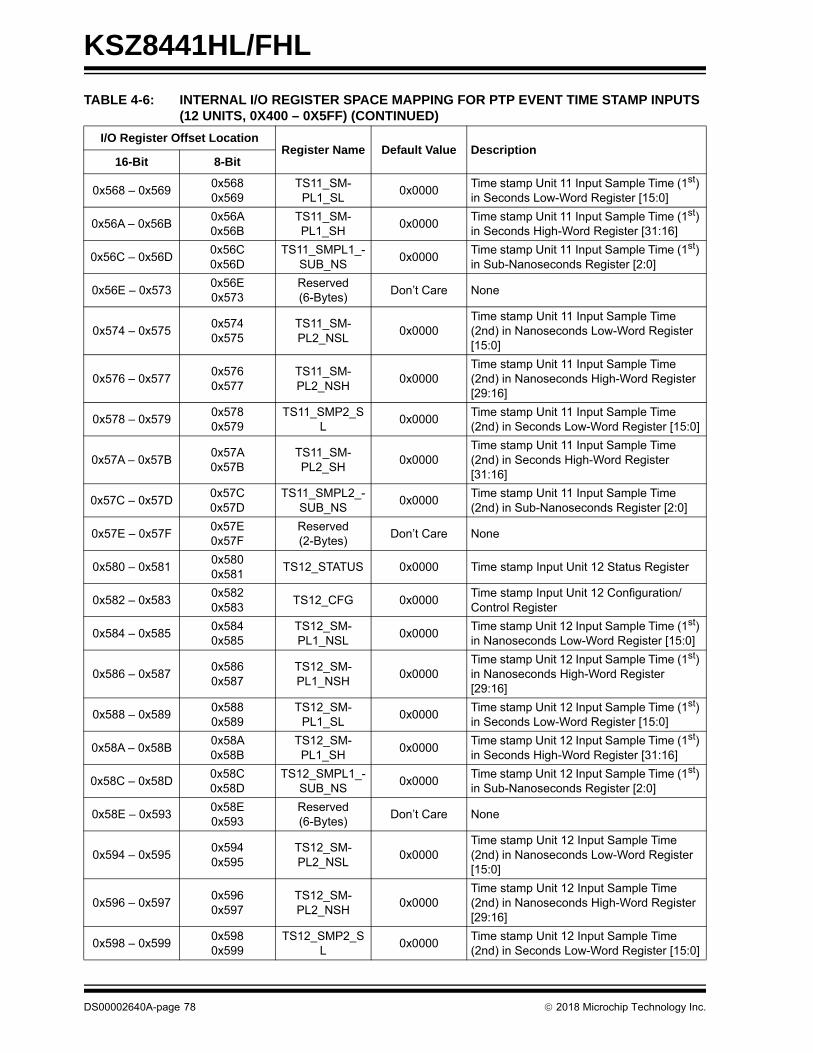
KSZ8441HL/FHL
0x568 – 0x5690x5680x569
TS11_SM-PL1_SL
0x0000Time stamp Unit 11 Input Sample Time (1st) in Seconds Low-Word Register [15:0]
0x56A – 0x56B0x56A0x56B
TS11_SM-PL1_SH
0x0000Time stamp Unit 11 Input Sample Time (1st) in Seconds High-Word Register [31:16]
0x56C – 0x56D0x56C0x56D
TS11_SMPL1_-SUB_NS
0x0000Time stamp Unit 11 Input Sample Time (1st) in Sub-Nanoseconds Register [2:0]
0x56E – 0x5730x56E0x573
Reserved(6-Bytes)
Don’t Care None
0x574 – 0x5750x5740x575
TS11_SM-PL2_NSL
0x0000Time stamp Unit 11 Input Sample Time (2nd) in Nanoseconds Low-Word Register [15:0]
0x576 – 0x5770x5760x577
TS11_SM-PL2_NSH
0x0000Time stamp Unit 11 Input Sample Time (2nd) in Nanoseconds High-Word Register [29:16]
0x578 – 0x5790x5780x579
TS11_SMP2_SL
0x0000Time stamp Unit 11 Input Sample Time (2nd) in Seconds Low-Word Register [15:0]
0x57A – 0x57B0x57A0x57B
TS11_SM-PL2_SH
0x0000Time stamp Unit 11 Input Sample Time (2nd) in Seconds High-Word Register [31:16]
0x57C – 0x57D0x57C0x57D
TS11_SMPL2_-SUB_NS
0x0000Time stamp Unit 11 Input Sample Time (2nd) in Sub-Nanoseconds Register [2:0]
0x57E – 0x57F0x57E0x57F
Reserved(2-Bytes)
Don’t Care None
0x580 – 0x5810x5800x581
TS12_STATUS 0x0000 Time stamp Input Unit 12 Status Register
0x582 – 0x5830x5820x583
TS12_CFG 0x0000Time stamp Input Unit 12 Configuration/Control Register
0x584 – 0x5850x5840x585
TS12_SM-PL1_NSL
0x0000Time stamp Unit 12 Input Sample Time (1st) in Nanoseconds Low-Word Register [15:0]
0x586 – 0x5870x5860x587
TS12_SM-PL1_NSH
0x0000Time stamp Unit 12 Input Sample Time (1st) in Nanoseconds High-Word Register [29:16]
0x588 – 0x5890x5880x589
TS12_SM-PL1_SL
0x0000Time stamp Unit 12 Input Sample Time (1st) in Seconds Low-Word Register [15:0]
0x58A – 0x58B0x58A0x58B
TS12_SM-PL1_SH
0x0000Time stamp Unit 12 Input Sample Time (1st) in Seconds High-Word Register [31:16]
0x58C – 0x58D0x58C0x58D
TS12_SMPL1_-SUB_NS
0x0000Time stamp Unit 12 Input Sample Time (1st) in Sub-Nanoseconds Register [2:0]
0x58E – 0x5930x58E0x593
Reserved(6-Bytes)
Don’t Care None
0x594 – 0x5950x5940x595
TS12_SM-PL2_NSL
0x0000Time stamp Unit 12 Input Sample Time (2nd) in Nanoseconds Low-Word Register [15:0]
0x596 – 0x5970x5960x597
TS12_SM-PL2_NSH
0x0000Time stamp Unit 12 Input Sample Time (2nd) in Nanoseconds High-Word Register [29:16]
0x598 – 0x5990x5980x599
TS12_SMP2_SL
0x0000Time stamp Unit 12 Input Sample Time (2nd) in Seconds Low-Word Register [15:0]
TABLE 4-6: INTERNAL I/O REGISTER SPACE MAPPING FOR PTP EVENT TIME STAMP INPUTS (12 UNITS, 0X400 – 0X5FF) (CONTINUED)
I/O Register Offset LocationRegister Name Default Value Description
16-Bit 8-Bit
DS00002640A-page 78 2018 Microchip Technology Inc.

KSZ8441HL/FHL
0x59A – 0x59B0x59A0x59B
TS12_SM-PL2_SH
0x0000Time stamp Unit 12 Input Sample Time (2nd) in Seconds High-Word Register [31:16]
0x59C – 0x59D0x59C0x59D
TS12_SMPL2_-SUB_NS
0x0000Time stamp Unit 12 Input Sample Time (2nd) in Sub-Nanoseconds Register [2:0]
0x59E – 0x5A30x59E0x5A3
Reserved(6-Bytes)
Don’t Care None
0x5A4 – 0x5A50x5A40x5A5
TS12_SM-PL3_NSL
0x0000Time stamp Unit 12 Input Sample Time (3rd) in Nanoseconds Low-Word Register [15:0]
0x5A6 – 0x5A70x5A60x5A7
TS12_SM-PL3_NSH
0x0000Time stamp Unit 12 Input Sample Time (3rd) in Nanoseconds High-Word Register [29:16]
0x5A8 – 0x5A90x5A80x5A9
TS12_SM-PL3_SL
0x0000Time stamp Unit 12 Input Sample Time (3rd) in Seconds Low-Word Register [15:0]
0x5AA – 0x5AB0x5AA0x5AB
TS12_SM-PL3_SH
0x0000Time stamp Unit 12 Input Sample Time (3rd) in Seconds High-Word Register [31:16]
0x5AC – 0x5AD0x5AC0x5AD
TS12_SMPL3_-SUB_NS
0x0000Time stamp Unit 12 Input Sample Time (3rd) in Sub-Nanoseconds Register [2:0]
0x5AE – 0x5B30x5AE0x5B3
Reserved(6-Bytes)
Don’t Care None
0x5B4 – 0x5B50x5B40x5B5
TS12_SM-PL4_NSL
0x0000Time stamp Unit 12 Input Sample Time (4th) in Nanoseconds Low-Word Register [15:0]
0x5B6 – 0x5B70x5B60x5B7
TS12_SM-PL4_NSH
0x0000Time stamp Unit 12 Input Sample Time (4th) in Nanoseconds High-Word Register [29:16]
0x5B8 – 0x5B90x5B80x5B9
TS12_SM-PL4_SL
0x0000Time stamp Unit 12 Input Sample Time (4th) in Seconds Low-Word Register [15:0]
0x5BA – 0x5BB0x5BA0x5BB
TS12_SM-PL4_SH
0x0000Time stamp Unit 12 Input Sample Time (4th) in Seconds High-Word Register [31:16]
0x5BC – 0x5BD0x5BC0x5BD
TS12_SMPL4_-SUB_NS
0x0000Time stamp Unit 12 Input Sample Time (4th) in Sub-Nanoseconds Register [2:0]
0x5BE – 0x5C30x5BE0x5C3
Reserved(6-Bytes)
Don’t Care None
0x5C4 – 0x5C50x5C40x5C5
TS12_SM-PL5_NSL
0x0000Time stamp Unit 12 Input Sample Time (5th) in Nanoseconds Low-Word Register [15:0]
0x5C6 – 0x5C70x5C60x5C7
TS12_SM-PL5_NSH
0x0000Time stamp Unit 12 Input Sample Time (5th) in Nanoseconds High-Word Register [29:16]
0x5C8 – 0x5C90x5C80x5C9
TS12_SM-PL5_SL
0x0000Time stamp Unit 12 Input Sample Time (5th) in Seconds Low-Word Register [15:0]
0x5CA – 0x5CB0x5CA0x5CB
TS12_SM-PL5_SH
0x0000Time stamp Unit 12 Input Sample Time (5th) in Seconds High-Word Register [31:16]
TABLE 4-6: INTERNAL I/O REGISTER SPACE MAPPING FOR PTP EVENT TIME STAMP INPUTS (12 UNITS, 0X400 – 0X5FF) (CONTINUED)
I/O Register Offset LocationRegister Name Default Value Description
16-Bit 8-Bit
2018 Microchip Technology Inc. DS00002640A-page 79

KSZ8441HL/FHL
0x5CC – 0x5CD0x5CC0x5CD
TS12_SMPL5_-SUB_NS
0x0000Time stamp Unit 12 Input Sample Time (5th) in Sub-Nanoseconds Register [2:0]
0x5CE – 0x5D30x5CE0x5D3
Reserved(6-Bytes)
Don’t Care None
0x5D4 – 0x5D50x5D40x5D5
TS12_SM-PL6_NSL
0x0000Time stamp Unit 12 Input Sample Time (6th) in Nanoseconds Low-Word Register [15:0]
0x5D6 – 0x5D70x5D60x5D7
TS12_SM-PL6_NSH
0x0000Time stamp Unit 12 Input Sample Time (6th) in Nanoseconds High-Word Register [29:16]
0x5D8 – 0x5D90x5D80x5D9
TS12_SM-PL6_SL
0x0000Time stamp Unit 12 Input Sample Time (6th) in Seconds Low-Word Register [15:0]
0x5DA – 0x5DB0x5DA0x5DB
TS12_SM-PL6_SH
0x0000Time stamp Unit 12 Input Sample Time (6th) in Seconds High-Word Register [31:16]
0x5DC – 0x5DD0x5DC0x5DD
TS12_SMPL6_-SUB_NS
0x0000Time stamp Unit 12 Input Sample Time (6th) in Sub-Nanoseconds Register [2:0]
0x5DE – 0x5E30x5DE0x5E3
Reserved(6-Bytes)
Don’t care None
0x5E4 – 0x5E50x5E40x5E5
TS12_SM-PL7_NSL
0x0000Time stamp Unit 12 Input Sample Time (7th) in Nanoseconds Low-Word Register [15:0]
0x5E6 – 0x5E70x5E60x5E7
TS12_SM-PL7_NSH
0x0000Time stamp Unit 12 Input Sample Time (7th) in Nanoseconds High-Word Register [29:16]
0x5E8 – 0x5E90x5E80x5E9
TS12_SM-PL7_SL
0x0000Time stamp Unit 12 Input Sample Time (7th) in Seconds Low-Word Register [15:0]
0x5EA – 0x5EB0x5EA0x5EB
TS12_SM-PL7_SH
0x0000Time stamp Unit 12 Input Sample Time (7th) in Seconds High-Word Register [31:16]
0x5EC – 0x5ED0x5EC0x5ED
TS12_SMPL7_-SUB_NS
0x0000Time stamp Unit 12 Input Sample Time (7th) in Sub-Nanoseconds Register [2:0]
0x5EE – 0x5F30x5EE0x5F3
Reserved(6-Bytes)
Don’t Care None
0x5F4 – 0x5F50x5F40x5F5
TS12_SM-PL8_NSL
0x0000Time stamp Unit 12 Input Sample Time (8th) in Nanoseconds Low-Word Register [15:0]
0x5F6 – 0x5F70x5F60x5F7
TS12_SM-PL8_NSH
0x0000Time stamp Unit 12 Input Sample Time (8th) in Nanoseconds High-Word Register [29:16]
0x5F8 – 0x5F90x5F80x5F9
TS12_SM-PL8_SL
0x0000Time stamp Unit 12 Input Sample Time (8th) in Seconds Low-Word Register [15:0]
0x5FA – 0x5FB0x5FA0x5FB
TS12_SM-PL8_SH
0x0000Time stamp Unit 12 Input Sample Time (8th) in Seconds High-Word Register [31:16]
0x5FC – 0x5FD0x5FC0x5FD
TS12_SMPL8_-SUB_NS
0x0000Time stamp Unit 12 Input Sample Time (8th) in Sub-Nanoseconds Register [2:0]
TABLE 4-6: INTERNAL I/O REGISTER SPACE MAPPING FOR PTP EVENT TIME STAMP INPUTS (12 UNITS, 0X400 – 0X5FF) (CONTINUED)
I/O Register Offset LocationRegister Name Default Value Description
16-Bit 8-Bit
DS00002640A-page 80 2018 Microchip Technology Inc.

KSZ8441HL/FHL
0x5FE – 0x5FF0x5FE0x5FF
Reserved(2-Bytes)
Don’t Care None
TABLE 4-7: INTERNAL I/O REGISTER SPACE MAPPING FOR PTP 1588 CLOCK AND GLOBAL CONTROL (0X600 – 0X7FF)
I/O Register Offset LocationRegister Name Default Value Description
16-Bit 8-Bit
0x600 – 0x6010x6000x601
PTP_CLK_CTL 0x0002 PTP Clock Control Register [6:0]
0x602 – 0x6030x6020x603
Reserved(2-Bytes)
Don’t care None
0x604 – 0x6050x6040x605
PTP_RTC_NSL 0x0000PTP Real Time Clock in Nanoseconds Low-Word Register [15:0]
0x606 – 0x6070x6060x607
PTP_RTC_NSH 0x0000PTP Real Time Clock in Nanoseconds High-Word Register [31:16]
0x608 – 0x6090x6080x609
PTP_RTC_SL 0x0000PTP Real Time Clock in Seconds Low-Word Register [15:0]
0x60A – 0x60B0x60A0x60B
PTP_RTC_SH 0x0000PTP Real Time Clock in Seconds High-Word Register [31:16]
0x60C – 0x60D0x60C0x60D
PTP_RT-C_PHASE
0x0000PTP Real Time Clock in Phase Register [2:0]
0x60E – 0x60F0x60E0x60F
Reserved(2-Bytes)
Don’t Care None
0x610 – 0x6110x6100x611
PTP_SNS_RATE_L
0x0000PTP Sub-nanosecond Rate Low-Word Reg-ister [15:0]
0x612 – 0x6130x6120x613
PTP_SNS_RATE_H
0x0000PTP Sub-nanosecond Rate High-Word [29:16] and Configuration Register
0x614 – 0x6150x6140x615
PTP_TEMP_-ADJ_DURA_L
0x0000PTP Temporary Adjustment Mode Duration Low-Word Register [15:0]
0x616 – 0x6170x6160x617
PTP_TEMP_-ADJ_DURA_H
0x0000PTP Temporary Adjustment Mode Duration High-Word Register [31:16]
0x618 – 0x61F0x6180x61F
Reserved(8-Bytes)
Don’t Care None
0x620 – 0x6210x6200x621
PTP_MSG_CF-G_1
0x0059PTP Message Configuration 1 Register [7:0]
0x622 – 0x6230x6220x623
PTP_MSG_CF-G_2
0x0404PTP Message Configuration 2 Register [10:0]
0x624 – 0x6250x6240x625
PTP_DO-MAIN_VER
0x0200 PTP Domain and Version Register [11:0]
0x626 – 0x63F0x6260x63F
Reserved(26-Bytes)
Don’t Care None
0x640 – 0x6410x6400x641
PTP_P1_RX_ LATENCY
0x019F PTP Port 1 Receive Latency Register [15:0]
0x642 – 0x6430x6420x643
PTP_P1_TX_ LATENCY
0x002DPTP Port 1 Transmit Latency Register [15:0]
0x644 – 0x6450x6440x645
PTP_P1_ASYM_COR
0x0000PTP Port 1 Asymmetry Correction Register [15:0]
TABLE 4-6: INTERNAL I/O REGISTER SPACE MAPPING FOR PTP EVENT TIME STAMP INPUTS (12 UNITS, 0X400 – 0X5FF) (CONTINUED)
I/O Register Offset LocationRegister Name Default Value Description
16-Bit 8-Bit
2018 Microchip Technology Inc. DS00002640A-page 81

KSZ8441HL/FHL
0x646 – 0x6470x6460x647
PTP_P1_LINK_DLY
0x0000 PTP Port 1 Link Delay Register [15:0]
0x648 – 0x6490x6480x649
P1_XD-LY_REQ_TSL
0x0000PTP Port 1 Egress Time stamp Low-Word for Pdelay_REQ and Delay_REQ Frames Register [15:0]
0x64A – 0x64B0x64A0x64B
P1_XD-LY_REQ_TSH
0x0000PTP Port 1 Egress Time stamp High-Word for Pdelay_REQ and Delay_REQ Frames Register [31:16]
0x64C – 0x64D0x64C0x64D
P1_SYNC_TSL 0x0000PTP Port 1 Egress Time stamp Low-Word for SYNC Frame Register [15:0]
0x64E – 0x64F0x64E0x64F
P1_SYNC_TSH 0x0000PTP Port 1 Egress Time stamp High-Word for SYNC Frame Register [31:16]
0x650 – 0x6510x6500x651
P1_PDLY_RE-SP_TSL
0x0000PTP Port 1 Egress Time stamp Low-Word for Pdelay_resp Frame Register [15:0]
0x652 – 0x6530x6520x653
P1_PDLY_RE-SP_TSH
0x0000PTP Port 1 Egress Time stamp High-Word for Pdelay_resp Frame Register [31:16]
0x654 – 0x67F0x6540x67F
Reserved(44-Bytes)
Don’t Care None
0x680 – 0x6810x6800x681
GPIO_MONI-TOR
0x0000 PTP GPIO Monitor Register [11:0]
0x682 – 0x6830x6820x683
GPIO_OEN 0x0000 PTP GPIO Output Enable Register [11:0]
0x684 – 0x6870x6840x687
Reserved(4-Bytes)
Don’t Care None
0x688 – 0x6890x6880x689
PTP_TRIG_IS 0x0000 PTP Trigger Unit Interrupt Status Register
0x68A – 0x68B0x68A0x68B
PTP_TRIG_IE 0x0000 PTP Trigger Unit Interrupt Enable Register
0x68C – 0x68D0x68C0x68D
PTP_TS_IS 0x0000PTP Time stamp Unit Interrupt Status Reg-ister
0x68E – 0x68F0x68E0x68F
PTP_TS_IE 0x0000PTP Time stamp Unit Interrupt Enable Reg-ister
0x690 – 0x7330x6900x733
Reserved(164-Bytes)
Don’t Care None
0x734 – 0x7350x7340x735
DSP_CNTRL_6 0x3020 DSP Control 1 Register
0x736 – 0x7470x7360x747
Reserved(18-Bytes)
Don’t Care None
0x748 – 0x7490x7480x749
ANA_CNTRL_1 0x0000 Analog Control 1 Register
0x74A – 0x74B0x74A0x74B
Reserved(2-Bytes)
Don’t Care None
0x74C – 0x74D0x74C0x74D
ANA_CNTRL_3 0x0000 Analog Control 3 Register
0x74E – 0x7FF0x74E0x7FF
Reserved(178-Bytes)
Don’t Care None
TABLE 4-7: INTERNAL I/O REGISTER SPACE MAPPING FOR PTP 1588 CLOCK AND GLOBAL CONTROL (0X600 – 0X7FF) (CONTINUED)
I/O Register Offset LocationRegister Name Default Value Description
16-Bit 8-Bit
DS00002640A-page 82 2018 Microchip Technology Inc.
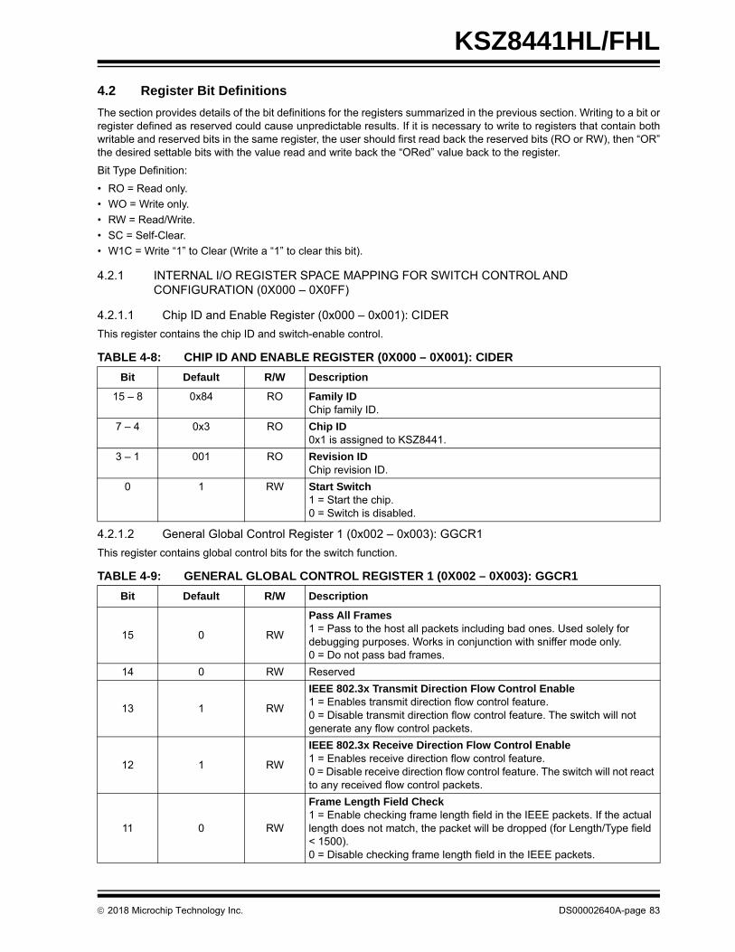
KSZ8441HL/FHL
4.2 Register Bit Definitions
The section provides details of the bit definitions for the registers summarized in the previous section. Writing to a bit orregister defined as reserved could cause unpredictable results. If it is necessary to write to registers that contain bothwritable and reserved bits in the same register, the user should first read back the reserved bits (RO or RW), then “OR”the desired settable bits with the value read and write back the “ORed” value back to the register.
Bit Type Definition:
• RO = Read only.
• WO = Write only.
• RW = Read/Write.
• SC = Self-Clear.
• W1C = Write “1” to Clear (Write a “1” to clear this bit).
4.2.1 INTERNAL I/O REGISTER SPACE MAPPING FOR SWITCH CONTROL AND CONFIGURATION (0X000 – 0X0FF)
4.2.1.1 Chip ID and Enable Register (0x000 – 0x001): CIDER
This register contains the chip ID and switch-enable control.
4.2.1.2 General Global Control Register 1 (0x002 – 0x003): GGCR1
This register contains global control bits for the switch function.
TABLE 4-8: CHIP ID AND ENABLE REGISTER (0X000 – 0X001): CIDER
Bit Default R/W Description
15 – 8 0x84 RO Family IDChip family ID.
7 – 4 0x3 RO Chip ID0x1 is assigned to KSZ8441.
3 – 1 001 RO Revision IDChip revision ID.
0 1 RW Start Switch1 = Start the chip.0 = Switch is disabled.
TABLE 4-9: GENERAL GLOBAL CONTROL REGISTER 1 (0X002 – 0X003): GGCR1
Bit Default R/W Description
15 0 RW
Pass All Frames1 = Pass to the host all packets including bad ones. Used solely for debugging purposes. Works in conjunction with sniffer mode only.0 = Do not pass bad frames.
14 0 RW Reserved
13 1 RW
IEEE 802.3x Transmit Direction Flow Control Enable1 = Enables transmit direction flow control feature.0 = Disable transmit direction flow control feature. The switch will not generate any flow control packets.
12 1 RW
IEEE 802.3x Receive Direction Flow Control Enable1 = Enables receive direction flow control feature.0 = Disable receive direction flow control feature. The switch will not react to any received flow control packets.
11 0 RW
Frame Length Field Check1 = Enable checking frame length field in the IEEE packets. If the actual length does not match, the packet will be dropped (for Length/Type field < 1500).0 = Disable checking frame length field in the IEEE packets.
2018 Microchip Technology Inc. DS00002640A-page 83

KSZ8441HL/FHL
4.2.1.3 0x004 – 0x00D: Reserved
4.2.1.4 General Global Control Register 7 (0x00E – 0x00F): GGCR7
This register contains global control bits for the switch function.
10 - 9 10 RW Reserved
8 0 RWAggressive Back-Off Enable1 = Enable more aggressive back-off algorithm in half-duplex mode to enhance performance. This is not an IEEE standard.
7 – 6 01 RW Reserved
5 0 RW
Enable Flow Control when Exceeding Ingress Limit1 = Flow control frame will be sent to link partner when exceeding the ingress rate limit.0 = Frame will be dropped when exceeding the ingress rate limit.
4 1 RW
Receive 2K Byte Packets Enable1 = Enable packet length up to 2K bytes. While set, GGCR2 bits[2,1] will have no effect.0 = Discard packet if packet length is greater than 2000 bytes.
3 - 0 0 RW Reserved
TABLE 4-10: GENERAL GLOBAL CONTROL REGISTER 7 (0X00E – 0X00F): SGCR7
Bit Default R/W Description
15 – 10 0x02 RW Reserved
9 – 8 0x0 RW
Port 1 LED Mode When read, these two bits provide the current setting of the LED display mode for P1LED1 and P1LED0 as defined as below. Reg. 0x06C – 0x06D, bits [14:12] determine if this automatic functionality is utilized or if the Port 1 LEDs are controlled by the local host processor.
LED Mode P1LED1 P1LED0
00 Speed Link and Activity
01 Activity Link
10 Full-Duplex Link and Activity
11 Full-Duplex Link
7 0 RW Reserved
6 – 5 01 or 10 RW
Driver Strength SelectionThese two bits determine the drive strength of all I/O pins except for the following category of pins: LED pins, GPIO pins, INTRN, RSTN, and RXD3/REFCLK_0.00 = 4 mA01 = 8 mA. (Default when VDD_IO is 3.3V or 2.5V)10 = 12 mA. (Default when VDD_IO is 1.8V)11 = 16 mA.
4 – 3 00 RW Reserved
2 – 0 111 RW Reserved
TABLE 4-9: GENERAL GLOBAL CONTROL REGISTER 1 (0X002 – 0X003): GGCR1 (CONTINUED)
Bit Default R/W Description
DS00002640A-page 84 2018 Microchip Technology Inc.

KSZ8441HL/FHL
4.2.2 MAC ADDRESS REGISTERS
4.2.2.1 MAC Address Register 1 (0x010 – 0x011): MACAR1
This register contains the two MSBs of the MAC address for the controller function. This MAC address is used for send-ing PAUSE frames.
4.2.2.2 MAC Address Register 2 (0x012 – 0x013): MACAR2
This register contains the MAC address for sending PAUSE frames.
4.2.2.3 MAC Address Register 3 (0x014 – 0x015): MACAR3
This register contains the two LSBs of the MAC address for sending PAUSE frames.
4.2.2.4 0x016 – 0x025: Reserved
4.2.3 INDIRECT ACCESS DATA REGISTERS
4.2.3.1 Indirect Access Data Register 1 (0x026 – 0x027): IADR1
This register is used to indirectly read or write the data in the MIB Counters. Refer to the MIB section that follows thissection for detailed bit information.
TABLE 4-11: MAC ADDRESS REGISTER 1 (0X010 – 0X011): MACAR1
Bit Default R/W Description
15 – 0 0x0010 RWMACA[47:32]Specifies MAC Address 1 for sending PAUSE frame.
TABLE 4-12: MAC ADDRESS REGISTER 2 (0X012 – 0X013): MACAR2
Bit Default R/W Description
15 – 0 0xA1FF RW MACA[31:16]Specifies MAC Address 2 for sending PAUSE frame.
TABLE 4-13: MAC ADDRESS REGISTER 3 (0X014 – 0X015): MACAR3
Bit Default R/W Description
15 – 0 0xFFFF RW MACA[15:0]Specifies MAC Address 3 for sending PAUSE frame.
TABLE 4-14: INDIRECT ACCESS DATA REGISTER 1 (0X026 – 0X027): IADR1
Bit Default R/W Description
15 – 8 0x00 RO Reserved
7 0 RO
CPU Read StatusFor statistics counter reads.1 = Read is still in progress.0 = Read has completed.
6 – 0 0x00 RO Reserved
2018 Microchip Technology Inc. DS00002640A-page 85

KSZ8441HL/FHL
4.2.3.2 0x028 – 0x02B: Reserved
4.2.3.3 Indirect Access Data Register 4 (0x02C – 0x02D): IADR4
This register is used to indirectly read or write the data in the MIB Counters. Refer to the MIB section that follows thissection for detailed bit information.
4.2.3.4 Indirect Access Data Register 5 (0x02E – 0x02F): IADR5
This register is used to indirectly read or write the data in the MIB Counters. Refer to the MIB section that follows thissection for detailed bit information.
4.2.3.5 Indirect Access Control Register (0x030 – 0x031): IACR
This register is used to indirectly read or write the data in the MIB Counters. Writing to IACR triggers a command. Reador write access is determined by Register bit [12]. Refer to the MIB section that follows this section for detailed bit infor-mation.
4.2.4 POWER MANAGEMENT CONTROL AND WAKE-UP EVENT STATUS
4.2.4.1 Power Management Control and Wake-Up Event Status (0x032 – 0x033): PMCTRL
This register controls the power management mode and provides wake-up event status.
TABLE 4-15: INDIRECT ACCESS DATA REGISTER 4 (0X02C – 0X02D): IADR4
Bit Default R/W Description
15 – 0 0x0000 RWIndirect Data [15:0]Bit[15:0] of indirect data.
TABLE 4-16: INDIRECT ACCESS DATA REGISTER 5 (0X02E – 0X02F): IADR5
Bit Default R/W Description
15 – 0 0x0000 RWIndirect Data [31:16]Bit[31:16] of indirect data.
TABLE 4-17: INDIRECT ACCESS CONTROL REGISTER (0X030 – 0X031): IACR
Bit Default R/W Description
15 – 13 000 RW Reserved
12 0 RWRead Enable1 = Read cycle is enabled (MIB Counter will be cleared after the read).0 = No operation.
11 – 10 00 RW
Table Select00 = Reserved.01 = Reserved.10 = Reserved.11 = MIB counter selected.
9 – 0 0x000 RWIndirect Address [9:0]Bit[9:0] of indirect address.
TABLE 4-18: POWER MANAGEMENT CONTROL AND WAKE-UP EVENT STATUS (0X032 – 0X033): PMCTRL
Bit Default R/W Description
15 – 6 0x000 RO Reserved.
5 0RW
(W1C)
Wake-Up Frame Detect Status1 = A wake-up frame has been detected at the host QMU (Write a “1” to clear).0 = No Wake-Up frame has been detected.
DS00002640A-page 86 2018 Microchip Technology Inc.

KSZ8441HL/FHL
4.2.4.2 Power Management Event Enable Register (0x034 – 0x035): PMEE
This register contains the power management event enable control bits.
4.2.5 GO SLEEP TIME AND CLOCK TREE POWER-DOWN CONTROL REGISTERS
4.2.5.1 Go Sleep Time Register (0x036 – 0x037): GST
This register contains the value which is used to control the minimum Go-Sleep time period when the device transitionsfrom normal power state to low power state in energy detect mode.
4 0RW
(W1C)
Magic Packet Detect Status1 = A Magic Packet has been detected at either port 1 (Write a “1” to clear).0 = No Magic Packet has been detected.
3 0RW
(W1C)
Link-Up Detect Status1 = A Link Up condition has been detected at either port 1 (Write a “1 “to clear).0 = No Link Up has been detected.
2 0RW
(W1C)
Energy Detect Status1 = Energy is detected at either port 1 (Write a “1” to clear).0 = No energy is detected.Note: This is not valid in fiber mode.
1 – 0 00 RW
Power Management ModeThese two bits are used to control device power management mode. 00 = Normal Mode.01 = Energy Detect Mode.10 = Global Soft Power-Down Mode. (Does not reset QMU registers)11 = Reserved.
TABLE 4-19: POWER MANAGEMENT EVENT ENABLE REGISTER (0X034 – 0X035): PMEE
Bit Default R/W Description
15 - 5 0x000 RW Reserved
4 0 RW PME Polarity:1 = The PME pin is active-high.0 = The PME pin is active-low.
3 0 RW PME Woken Up By Wake-Up Frame Enable1 = The PME pin will be asserted when a wake-up frame is detected.0 = PME won’t be asserted by the wake-up frame detection
2 0 RW PME Woken Up By Magic Packet Enable1 = The PME pin will be asserted when a magic packet is detected.0 = PME won’t be asserted by the magic packet detection
1 0 RW PME Woken Up By Link-Up Enable1 = The PME pin will be asserted when a link-up is detected at port 1.0 = PME won’t be asserted by the link-up detection
0 0 RW PME Woken Up By Energy Detect Enable1 = The PME pin will be asserted when energy on line is detected at port 1.0 = PME won’t be asserted by the energy detection.
TABLE 4-20: GO SLEEP TIME REGISTER (0X036 – 0X037): GST
Bit Default R/W Description
15 – 8 0x00 RO Reserved
TABLE 4-18: POWER MANAGEMENT CONTROL AND WAKE-UP EVENT STATUS (0X032 – 0X033): PMCTRL (CONTINUED)
Bit Default R/W Description
2018 Microchip Technology Inc. DS00002640A-page 87
KSZ8441HL/FHL
4.2.5.2 Clock Tree Power-Down Control Register (0x038 – 0x039): CTPDC
This register contains the power-down control bits for all clocks.
4.2.5.3 0x03A – 0x04B: Reserved
4.2.6 PHY AND MII BASIC CONTROL REGISTERS
4.2.6.1 PHY 1 and MII Basic Control Register (0x04C – 0x04D): P1MBCR
This register contains media independent interface (MII) control bits for the switch port 1 function as defined in the IEEE802.3 specification.
7 – 0 0x8E RW
Go Sleep TimeThis value is used to control the minimum period the no energy event has to be detected consecutively before the device enters the low power state during energy-detect mode.The unit is 20 ms. The default go sleep time is around 3.0 seconds.
TABLE 4-21: CLOCK TREE POWER-DOWN CONTROL REGISTER (0X038 – 0X039): CTPDC
Bit Default R/W Description
15 – 5 0x000 RO Reserved
4 0 RW Reserved
3 0 RW
Switch Clock Auto Shut Down Enable1 = When no packet transfer is detected on the MII interface of port 1 for longer than the time specified in bit[1:0] of current register, the device will shut down the switch clock automatically. The switch clock will be woken up automatically when the MII interface of any port becomes busy.0 = Switch clock is always on.
2 0 RW
CPU Clock Auto Shutdown Enable1 = When no packet transfer is detected both on host interface and on MII interface of port 1 for longer than the time specified in bit[1:0] of cur-rent register, the device will shut down CPU clock automatically. The CPU clock will be waked up automatically when host activity is detected or MII interface of any port becomes busy.0 = CPU clock is always on.
1 – 0 00 RW
Shutdown Wait PeriodThese two bits specify the time for device to monitor host/MII activity con-tinuously before it could shut down switch or CPU clock.00 = 5.3s.01 = 1.6s.10 = 1 ms.11 = 3.2 µs.
TABLE 4-22: PHY 1 AND MII BASIC CONTROL REGISTER (0X04C – 0X04D): P1MBCR
Bit Default R/W Description Bit is Same As
15 0 RO Reserved —
14 0 RW
Far-End Loopback1 = Perform loopback as follows: Start: Host interface. Loopback: PMD/PMA of port 1’s PHY End: Host interface.0 = Normal operation.
Bit[14] in P1CR4
TABLE 4-20: GO SLEEP TIME REGISTER (0X036 – 0X037): GST (CONTINUED)
Bit Default R/W Description
DS00002640A-page 88 2018 Microchip Technology Inc.

KSZ8441HL/FHL
13 1 RW
Force 100BASE-TX1 = Force 100 Mbps if auto-negotiation is disabled (bit [12])0 = Force 10 Mbps if auto-negotiation is disabled (bit [12])
Bit[6] in P1CR4
12 1 RWAuto-Negotiation Enable1 = Auto-negotiation enabled.0 = Auto-negotiation disabled.
Bit[7] in P1CR4
11 0 RWPower-Down1 = Power-down.0 = Normal operation.
Bit[11] in P1CR4
10 0 ROIsolateNot supported.
—
9 0 RW/SCRestart Auto-Negotiation1 = Restart auto-negotiation.0 = Normal operation.
Bit[13] in P1CR4
8 1 RW
Force Full-Duplex1 = Force full-duplex.0 = Force half-duplex.Applies only when auto-negotiation is disabled (bit [12]).It is always in half-duplex if auto-negotiation is enabled but failed.
Bit[5] in P1CR4
7 0 ROCollision testNot supported.
—
6 0 RO Reserved. —
5 1 RWHP_MDIX1 = HP Auto-MDI-X mode.0 = Microchip Auto-MDI-X mode.
Bit[15] in P1SR
4 0 RWForce MDI-X1 = Force MDI-X.0 = Normal operation.
Bit[9] in P1CR4
3 0 RWDisable Auto-MDI-X1 = Disable Auto-MDI-X.0 = Normal operation.
Bit[10] in P1CR4
2 0 RW
Disable Far-End-Fault1 = Disable far-end-fault detection.0 = Normal operation.For 100BASE-FX fiber mode operation.
Bit[12] in P1CR4
1 0 RWDisable Transmit1 = Disable transmit.0 = Normal operation.
Bit[14] in P1CR4
0 0 RW Reserved —
TABLE 4-22: PHY 1 AND MII BASIC CONTROL REGISTER (0X04C – 0X04D): P1MBCR (CONTINUED)
Bit Default R/W Description Bit is Same As
2018 Microchip Technology Inc. DS00002640A-page 89

KSZ8441HL/FHL
4.2.6.2 PHY 1 and MII Basic Status Register (0x04E – 0x04F): P1MBSR
This register contains the media independent interface (MII) status bits for the switch port 1 function.
4.2.6.3 PHY 1 PHYID Low Register (0x050 – 0x051): PHY1ILR
This register contains the PHY ID (low) for port 1.
TABLE 4-23: PHY 1 AND MII BASIC STATUS REGISTER (0X04E – 0X04F): P1MBSR
Bit Default R/W Description Bit is Same As
15 0 ROT4 Capable1 = 100BASE-T4 capable.0 = Not 100BASE-T4 capable.
—
14 1 RO100BASE-TX Full Capable1 = 100BASE-TX full-duplex capable.0 = Not 100BASE-TX full-duplex capable.
—
13 1 RO100BASE-TX Half Capable1 = 100BASE-TX half-duplex capable.0 = Not 100BASE-TX half-duplex capable.
—
12 1 RO10BASE-T Full Capable1 = 10BASE-T full-duplex capable.0 = Not 10BASE-T full-duplex capable.
—
11 1 RO10BASE-T Half Capable1 = 10BASE-T half-duplex capable.0 = Not 10BASE-T half-duplex capable.
—
10 – 7 0x0 RO Reserved —
6 0 ROPreamble SuppressedNot supported.
—
5 0 ROAuto-Negotiation Complete1 = Auto-negotiation complete.0 = Auto-negotiation not completed.
Bit[6] in P1SR
4 0 RO
Far-End-Fault1 = Far-end-fault detected.0 = No far-end-fault detected.For 100BASE-FX fiber mode operation.
Bit[8] in P1SR
3 1 ROAuto-Negotiation Capable1 = Auto-negotiation capable.0 = Not auto-negotiation capable.
—
2 0 ROLink Status1 = Link is up.0 = Link is down.
Bit[5] in P1SR
1 0 ROJabber testNot supported.
—
0 0 ROExtended Capable1 = Extended register capable.0 = Not extended register capable.
—
TABLE 4-24: PHY 1 PHYID LOW REGISTER (0X050 – 0X051): PHY1ILR
Bit Default R/W Description
15 – 0 0x1430 ROPHY 1 ID Low WordLow order PHY 1 ID bits.
DS00002640A-page 90 2018 Microchip Technology Inc.
KSZ8441HL/FHL
4.2.6.4 PHY 1 PHYID High Register (0x052 – 0x053): PHY1IHR
This register contains the PHY ID (high) for port 1.
4.2.6.5 PHY 1 Auto-Negotiation Advertisement Register (0x054 – 0x055): P1ANAR
This register contains the auto-negotiation advertisement bits for port 1.
4.2.6.6 PHY 1 Auto-Negotiation Link Partner Ability Register (0x056 – 0x057): P1ANLPR
This register contains the auto-negotiation link partner ability bits for the switch port 1 function.
TABLE 4-25: PHY 1 PHYID HIGH REGISTER (0X052 – 0X053): PHY1IHR
Bit Default R/W Description
15 – 0 0x0022 ROPHY 1 ID High WordHigh-order PHY 1 ID bits.
TABLE 4-26: PHY 1 AUTO-NEGOTIATION ADVERTISEMENT REGISTER (0X054 – 0X055): P1ANAR
Bit Default R/W Description Bit is Same As
15 0 RONext pageNot supported.
—
14 0 RO Reserved —
13 0 RORemote faultNot supported.
—
12 – 11 00 RO Reserved —
10 1 RWPause (flow control capability)1 = Advertise pause ability.0 = Do not advertise pause capability.
Bit[4] in P1CR4
9 0 RW Reserved —
8 1 RW
Advertise 100BASE-TX Full-Duplex1 = Advertise 100BASE-TX full-duplex capable.0 = Do not advertise 100BASE-TX full-duplex capabil-ity.
Bit[3] in P1CR4
7 1 RW
Advertise 100BASE-TX Half-Duplex1= Advertise 100BASE-TX half-duplex capable.0 = Do not advertise 100BASE-TX half-duplex capabil-ity.
Bit[2] in P1CR4
6 1 RWAdvertise 10BASE-T Full-Duplex1 = Advertise 10BASE-T full-duplex capable.0 = Do not advertise 10BASE-T full-duplex capability.
Bit[1] in P1CR4
5 1 RWAdvertise 10BASE-T Half-Duplex1 = Advertise 10BASE-T half-duplex capable.0 = Do not advertise 10BASE-T half-duplex capability.
Bit[0] in P1CR4
4 – 0 0x01 ROSelector Field802.3
—
TABLE 4-27: PHY 1 AUTO-NEGOTIATION LINK PARTNER ABILITY REGISTER (0X056 – 0X057): P1ANLPR
Bit Default R/W Description Bit is Same As
15 0 RONext pageNot supported.
—
14 0 ROLP ACKNot supported.
—
13 0 RORemote faultNot supported.
—
2018 Microchip Technology Inc. DS00002640A-page 91

KSZ8441HL/FHL
4.2.6.7 0x058 – 0x065: Reserved
4.2.6.8 PHY1 Special Control and Status Register (0x066 – 0x067): P1PHYCTRL
This register contains control and status information of PHY 1.
4.2.6.9 0x068 – 0x06B: Reserved
12 - 11 00 RO Reserved —
10 0 ROPauseLink partner pause capability.
Bit[4] in P1SR
9 0 RO Reserved —
8 0 ROAdvertise 100BASE-TX Full-DuplexLink partner 100BASE-TX full-duplex capability.
Bit[3] in P1SR
7 0 ROAdvertise 100BASE-TX Half-DuplexLink partner 100 half-duplex capability.
Bit[2] in P1SR
6 0 ROAdvertise 10BASE-T Full-DuplexLink partner 10BASE-T full-duplex capability.
Bit[1] in P1SR
5 0 ROAdvertise 10BASE-T Half-DuplexLink partner 10BASE-T half-duplex capability.
Bit[0] in P1SR
4 - 0 0x01 RO Reserved —
TABLE 4-28: PHY1 SPECIAL CONTROL AND STATUS REGISTER (0X066 – 0X067): P1PHYCTRL
Bit Default R/W Description Bit is Same As
15 - 6 0x000 RO Reserved —
5 0 ROPolarity Reverse1 = Polarity is reversed.0 = Polarity is not reversed.
Bit[13] in P1SR
4 0 ROMDI-X Status0 = MDI1 = MDI-X
Bit[7] in P1SR
3 0 RWForce Link1 = Force link pass.0 = Normal operation.
Bit[11] in P1SCSLMD
2 1 RW
Enable Energy Efficient Ethernet (EEE) on 10BASE-Te 1 = Disable 10BASE-Te.0 = Enable 10BASE-Te.
—
1 0 RW
Remote (Near-End) Loopback1 = Perform remote loopback at port 1's PHY (RXP1/RXM1 -> TXP1/TXM1)0 = Normal operation
Bit[9] in P1SCSLMD
0 0 RW Reserved —
TABLE 4-27: PHY 1 AUTO-NEGOTIATION LINK PARTNER ABILITY REGISTER (0X056 – 0X057): P1ANLPR (CONTINUED)
Bit Default R/W Description Bit is Same As
DS00002640A-page 92 2018 Microchip Technology Inc.

KSZ8441HL/FHL
4.2.7 PORT 1 CONTROL REGISTERS
4.2.7.1 Port 1 Control Register 1 (0x06C – 0x06D): P1CR1
This register contains control bits for Port 1 functions.
4.2.7.2 0x06E – 0x07B: Reserved
4.2.7.3 Port 1 PHY Special Control/Status, LinkMD (0x07C – 0x07D): P1SCSLMD
This register contains the LinkMD control and status information of PHY 1.
4.2.7.4 Port 1 Control Register 4 (0x07E – 0x07F): P1CR4
This register contains control bits for the switch port 1 function.
TABLE 4-29: PORT 1 CONTROL REGISTER 1 (0X06C – 0X06D): P1CR1
Bit Default R/W Description
15 0 RO Reserved
14 - 12 000 RW
Port 1 LED Direct ControlThese bits directly control the port 1 LED pins.0xx = Normal LED function as set up via Reg. 0x00E – 0x00F, Bits[9:8].100 = Both port 1 LEDs off.101 = Port 1 LED1 off, LED0 on.110 = Port 1 LED1 on, LED0 off.111 = Both port 1 LEDs on.
11 - 0 0x000 RW Reserved
TABLE 4-30: PORT 1 PHY SPECIAL CONTROL/STATUS, LINKMD (0X07C – 0X07D): P1SCSLMD
Bit Default R/W Description Bit is Same As
15 0 ROCDT_10m_Short1 = Less than 10 meter short.
—
14 - 13 00 RO
Cable Diagnostic Test Results[00] = Normal condition.[01] = Open condition has been detected in cable.[10] = Short condition has been detected in cable.[11] = Cable diagnostic test has failed.
—
12 0 RW/SC
Cable Diagnostic Test Enable 1 = Cable diagnostic test is enabled. It is self-cleared after the test is done.0 = Indicates that the cable diagnostic test has com-pleted and the status information is valid for reading.
—
11 0 RWForce_Link1 = Force link pass.0 = Normal operation.
Bit[3] in P1PHYCTRL
10 1 RW Reserved —
9 0 RW
Remote (Near-End) Loopback1 = Perform remote loopback at port 1's PHY (RXP1/RXM1 -> TXP1/TXM1)0 = Normal operation
Bit[1] in P1PHYCTRL
8 - 0 0x000 ROCDT_Fault_CountDistance to the fault. It’s approximately 0.4m*CDT_-Fault_Count.
—
TABLE 4-31: PORT 1 CONTROL REGISTER 4 (0X07E – 0X07F): P1CR4
Bit Default R/W Description Bit is Same As
15 0 RW Reserved —
2018 Microchip Technology Inc. DS00002640A-page 93

KSZ8441HL/FHL
14 0 RWDisable Transmit1 = Disable the port’s transmitter.0 = Normal operation.
Bit[1] in P1MBCR
13 0 RW/SCRestart Auto-Negotiation1 = Restart auto-negotiation.0 = Normal operation.
Bit[9] in P1MBCR
12 0 RW
Disable Far-End-Fault1 = Disable far-end-fault detection.0 = Normal operation.For 100BASE-FX fiber mode operation.
Bit[2] in P1MBCR
11 0 RW
Power Down1 = Power down.0 = Normal operation.No change to registers setting.
Bit[11] in P1MBCR
10 0 RWDisable Auto-MDI/MDI-X1 = Disable Auto-MDI/MDI-X function.0 = Enable Auto-MDI/MDI-X function.
Bit[3] in P1MBCR
9 0 RW
Force MDI-X1 = If Auto-MDI/MDI-X is disabled, force PHY into MDI-X mode.0 = Do not force PHY into MDI-X mode.
Bit[4] in P1MBCR
8 0 RW
Far-End Loopback1 = Perform loopback, as indicated: Start: Host interface. Loopback: PMD/PMA of port 1’s PHY. End: Host interface.0 = Normal operation.
Bit[14] in P1MBCR
7 1 RW
Auto-Negotiation Enable1 = Auto-negotiation is enabled.0 = Disable auto-negotiation, speed, and duplex are decided by bits[6:5] of the same register.
Bit[12] in P1MBCR
6 1 RW
Force Speed1 = Force 100BASE-TX if auto-negotiation is disabled (bit[7]).0 = Force 10BASE-T if auto-negotiation is disabled (bit[7]).
Bit[13] in P1MBCR
5 1 RW
Force Duplex1 = Force full-duplex if auto-negotiation is disabled.0 = Force half-duplex if auto-negotiation is disabled.It is always in half-duplex if auto-negotiation is enabled but failed.
Bit[8] in P1MBCR
4 1 RW
Advertised Flow Control Capability1 = Advertise flow control (pause) capability.0 = Suppress flow control (pause) capability from transmission to link partner.
Bit[10] in P1ANAR
3 1 RW
Advertised 100BASE-TX Full-Duplex Capability1 = Advertise 100BASE-TX full-duplex capability.0 = Suppress 100BASE-TX full-duplex capability from transmission to link partner.
Bit [8] in P1ANAR
2 1 RW
Advertised 100BASE-TX Half-Duplex Capability1 = Advertise 100BASE-TX half-duplex capability.0 = Suppress 100BASE-TX half-duplex capability from transmission to link partner.
Bit[7] in P1ANAR
TABLE 4-31: PORT 1 CONTROL REGISTER 4 (0X07E – 0X07F): P1CR4 (CONTINUED)
Bit Default R/W Description Bit is Same As
DS00002640A-page 94 2018 Microchip Technology Inc.

KSZ8441HL/FHL
4.2.7.5 Port 1 Status Register (0x080 – 0x081): P1SR
This register contains status bits for port 1.
1 1 RW
Advertised 10BASE-T Full-Duplex Capability1 = Advertise 10BASE-T full-duplex capability.0 = Suppress 10BASE-T full-duplex capability from transmission to link partner.
Bit[6] in P1ANAR
0 1 RW
Advertised 10BASE-T Half-Duplex Capability1 = Advertise 10BASE-T half-duplex capability.0 = Suppress 10BASE-T half-duplex capability from transmission to link partner.
Bit[5] in P1ANAR
TABLE 4-32: PORT 1 STATUS REGISTER (0X080 – 0X081): P1SR
Bit Default R/W Description Bit is Same As
15 1 RWHP_Mdix1 = HP Auto-MDI-X mode.0 = Microchip Auto-MDI-X mode.
Bit[5] in P1MBCR
14 0 RO Reserved —
13 0 ROPolarity Reverse 1 = Polarity is reversed.0 = Polarity is not reversed.
Bit[5] in P1PHYCTRL
12 0 ROTransmit Flow Control Enable1 = Transmit flow control feature is active.0 = Transmit flow control feature is inactive.
—
11 0 RO
Receive Flow Control Enable1 = Receive flow control feature is active.0 = Receive flow control feature is inactive.Transmit Flow Control Enable1 = Transmit flow control feature is active.0 = Transmit flow control feature is inactive.
—
10 0 ROOperation Speed1 = Link speed is 100 Mbps.0 = Link speed is 10 Mbps.
—
9 0 ROOperation Duplex1 = Link duplex is full.0 = Link duplex is half.
—
8 0 RO Reserved —
7 0 ROMDI-X Status0 = MDI.1 = MDI-X.
Bit[4] in P1PHYCTRL
6 0 ROAuto-Negotiation Done1 = Auto-negotiation done.0 = Auto-negotiation not done.
Bit[5] in P1MBSR
5 0 ROLink Status1 = Link good.0 = Link not good.
Bit[2] in P1MBSR
4 0 ROPartner Flow Control Capability1 = Link partner flow control (pause) capable.0 = Link partner not flow control (pause) capable.
Bit[10] in P1ANLPR
3 0 ROPartner 100BASE-TX Full-Duplex Capability1 = Link partner 100BASE-TX full-duplex capable.0 = Link partner not 100BASE-TX full-duplex capable.
Bit[8] in P1ANLPR
TABLE 4-31: PORT 1 CONTROL REGISTER 4 (0X07E – 0X07F): P1CR4 (CONTINUED)
Bit Default R/W Description Bit is Same As
2018 Microchip Technology Inc. DS00002640A-page 95

KSZ8441HL/FHL
4.2.7.6 0x082 – 0x0D5: Reserved
4.2.8 INPUT AND OUTPUT MULTIPLEX SELECTION REGISTER
4.2.8.1 Input and Output Multiplex Selection Register (0x0D6 – 0x0D7): IOMXSEL
This register is used to select input/output pin functions of Pins 53, 54, and 55.
4.2.9 CONFIGURATION STATUS AND SERIAL BUS MODE REGISTER
4.2.9.1 Configuration Status and Serial Bus Mode Register (0x0D8 – 0x0D9): CFGR
This register is used to select fiber mode, if desired.
2 0 ROPartner 100BASE-TX Half-Duplex Capability1 = Link partner 100BASE-TX half-duplex capable.0= Link partner not 100BASE-TX half-duplex capable.
Bit[7] in P1ANLPR
1 0 ROPartner 10BASE-T Full-Duplex Capability1= Link partner 10BASE-T full-duplex capable.0 = Link partner not 10BASE-T full-duplex capable.
Bit[6] in P1ANLPR
0 0 ROPartner 10BASE-T Half-Duplex Capability1 = Link partner 10BASE-T half-duplex capable.0 = Link partner not 10BASE-T half-duplex capable.
Bit[5] in P1ANLPR
TABLE 4-33: INPUT AND OUTPUT MULTIPLEX SELECTION REGISTER (0X0D6 – 0X0D7): IOMXSEL
Bit Default R/W Description
15 - 12 0x0 RO Reserved
11 1 RW Reserved
10 1 RW Reserved
9 1 RW Reserved
8 1 RW Reserved
7 1 RW Reserved
6 1 RW Reserved
5 1 RWSelection of EESK or GPIO3 on Pin 531 = This pin is used for EESK (default), serial EEPROM clock.0 = This pin is used for GPIO3.
4 1 RW Reserved
3 1 RW Reserved
2 1 RWSelection of EEDIO or GPIO4 on Pin 54 1 = This pin is used for EEDIO (default), serial EEPROM data.0 = This pin is used for GPIO4.
1 1 RWSelection of EECS or GPIO5 on Pin 55 1 = This pin is used for EECS (default), serial EEPROM chip select.0 = This pin is used for GPIO5.
0 1 RW Reserved
TABLE 4-34: CONFIGURATION STATUS AND SERIAL BUS MODE REGISTER (0X0D8 – 0X0D9): CFGR
Bit Default R/W Description
15 - 8 0x00 RO Reserved
7 1 RW Reserved
TABLE 4-32: PORT 1 STATUS REGISTER (0X080 – 0X081): P1SR (CONTINUED)
Bit Default R/W Description Bit is Same As
DS00002640A-page 96 2018 Microchip Technology Inc.

KSZ8441HL/FHL
4.2.9.2 0x0DA – 0x0DB: Reserved
4.2.10 AUTO-NEGOTIATION NEXT PAGE REGISTERS
4.2.10.1 Port 1 Auto-Negotiation Next Page Transmit Register (0x0DC – 0x0DD): P1ANPT
This register contains the port 1 auto-negotiation next page transmit related bits.
6 1 RW
Selection of Port 1 Mode of Operation1 = Select copper mode0 = Select fiber mode (bypass MLT3 encoder/decoder, scrambler and descrambler). Fiber mode is available only for the KSZ8441FHL. When fiber mode is selected, bit [13] in DSP_CNTRL_6 (0x734 – 0x735) should be cleared.
5 - 4 11 RO Reserved
3 - 0 0xE RW Reserved
TABLE 4-35: PORT 1 AUTO-NEGOTIATION NEXT PAGE TRANSMIT REGISTER (0X0DC – 0X0DD): P1ANPT
Bit Default R/W Description
15 0 RO
Next PageNext Page (NP) is used by the Next Page function to indicate whether or not this is the last Next Page to be transmitted. NP shall be set as fol-lows:1 = Additional Next Page(s) will follow.0 = Last page.
14 0 RO Reserved
13 1 RO
Message Page Message Page (MP) is used by the Next Page function to differentiate a Message Page from an Unformatted Page. MP shall be set as follows:1 = Message Page.0 = Unformatted Page.
12 0 RO
Acknowledge 2Acknowledge 2 (Ack2) is used by the Next Page function to indicate that a device has the ability to comply with the message. Ack2 shall be set as follows:1 = Able to comply with message.0 = Unable to comply with message.
11 0 RO
ToggleToggle (T) is used by the arbitration function to ensure synchronization with the link partner during Next Page exchange. This bit shall always take the opposite value of the Toggle bit in the previously exchanged Link Codeword. The initial value of the Toggle bit in the first Next Page trans-mitted is the inverse of bit [11] in the base Link Codeword and, therefore, may assume a value of logic one or zero. The Toggle bit shall be set as follows:1 = Previous value of the transmitted Link Codeword equal to logic zero.0 = Previous value of the transmitted Link Codeword equal to logic one.
10 - 0 0x001 ROMessage and Unformatted Code FieldMessage/Unformatted code field bit[10:0]
TABLE 4-34: CONFIGURATION STATUS AND SERIAL BUS MODE REGISTER (0X0D8 – 0X0D9): CFGR (CONTINUED)
Bit Default R/W Description
2018 Microchip Technology Inc. DS00002640A-page 97

KSZ8441HL/FHL
4.2.10.2 Port 1 Auto-Negotiation Link Partner Received Next Page Register (0x0DE – 0x0DF): P1ALPRNP
This register contains the port 1 auto-negotiation link partner received next page related bits.
4.2.11 EEE AND LINK PARTNER ADVERTISEMENT REGISTERS
4.2.11.1 Port 1 EEE and Link Partner Advertisement Register (0x0E0 – 0x0E1): P1EEEA
This register contains the port 1 EEE advertisement and link partner advertisement information. Note that EEE is notsupported in fiber mode.
TABLE 4-36: PORT 1 AUTO-NEGOTIATION LINK PARTNER RECEIVED NEXT PAGE REGISTER (0X0DE – 0X0DF): P1ALPRNP
Bit Default R/W Description
15 0 RO
Next PageNext Page (NP) is used by the Next Page function to indicate whether or not this is the last Next Page to be transmitted. NP shall be set as fol-lows:1 = Additional Next Page(s) will follow.0 = Last page.
14 0 RO
AcknowledgeAcknowledge (Ack) is used by the auto-negotiation function to indicate that a device has successfully received its Link Partner’s Link Codeword. The Acknowledge bit is encoded in bit 14 regardless of the value of the Selector Field or Link Codeword encoding. If no Next Page information is to be sent, this bit shall be set to logic one in the Link Codeword after the reception of at least three consecutive and consistent FLP Bursts (ignor-ing the Acknowledge bit value).
13 0 RO
Message Page Message Page (MP) is used by the Next Page function to differentiate a Message Page from an Unformatted Page. MP shall be set as follows:1 = Message Page.0 = Unformatted Page.
12 0 RO
Acknowledge 2Acknowledge 2 (Ack2) is used by the Next Page function to indicate that a device has the ability to comply with the message. Ack2 shall be set as follows:1 = Able to comply with message.0 = Unable to comply with message.
11 0 RO
ToggleToggle (T) is used by the arbitration function to ensure synchronization with the link partner during Next Page exchange. This bit shall always take the opposite value of the Toggle bit in the previously exchanged Link Codeword. The initial value of the Toggle bit in the first Next Page trans-mitted is the inverse of bit [11] in the base Link Codeword and, therefore, may assume a value of logic one or zero. The Toggle bit shall be set as follows:1 = Previous value of the transmitted Link Codeword equal to logic zero.0 = Previous value of the transmitted Link Codeword equal to logic one.
10 - 0 0x000 ROMessage and Unformatted Code FieldMessage/Unformatted code field bit[10:0]
TABLE 4-37: PORT 1 EEE AND LINK PARTNER ADVERTISEMENT REGISTER (0X0E0 – 0X0E1): P1EEEA
Bit Default R/W Description
15 0 RO Reserved
DS00002640A-page 98 2018 Microchip Technology Inc.

KSZ8441HL/FHL
4.2.11.2 Port 1 EEE Wake Error Count Register (0x0E2 – 0x0E3): P1EEEWEC
This register contains the port 1 EEE wake error count information. Note that EEE is not supported in Fiber mode.
14 0 RO10GBASE-KR EEE1 = Link Partner EEE is supported for 10GBASE-KR.0 = Link Partner EEE is not supported for 10GBASE-KR.
13 0 RO10GBASE-KX4 EEE1 = Link Partner EEE is supported for 10GBASE-KX4.0 = Link Partner EEE is not supported for 10GBASE-KX4.
12 0 RO1000BASE-KX EEE1 = Link Partner EEE is supported for 1000BASE-KX.0 = Link Partner EEE is not supported for 1000BASE-KX.
11 0 RO10GBASE-T EEE1 = Link Partner EEE is supported for 10GBASE-T.0 = Link Partner EEE is not supported for 10GBASE-T.
10 0 RO1000BASE-T EEE1 = Link Partner EEE is supported for 1000BASE-T.0 = Link Partner EEE is not supported for 1000BASE-T.
9 0 RO100BASE-TX EEE1 = Link Partner EEE is supported for 100BASE-TX.0 = Link Partner EEE is not supported for 100BASE-TX.
8 - 7 00 RO Reserved
6 0 RO10GBASE-KR EEE1 = Port 1 EEE is supported for 10GBASE-KR.0 = Port 1 EEE is not supported for 10GBASE-KR.
5 0 RO10GBASE-KX4 EEE1 = Port 1 EEE is supported for 10GBASE-KX4.0 = Port 1 EEE is not supported for 10GBASE-KX4.
4 0 RO1000BASE-KX EEE1 = Port 1 EEE is supported for 1000BASE-KX.0 = Port 1 EEE is not supported for 1000BASE-KX.
3 0 RO10GBASE-T EEE1 = Port 1 EEE is supported for 10GBASE-T.0 = Port 1 EEE is not supported for 10GBASE-T.
2 0 RO1000BASE-T EEE1 = Port 1 EEE is supported for 1000BASE-T.0 = Port 1 EEE is not supported for 1000BASE-T.
1 1 RW
100BASE-TX EEE1 = Port 1 EEE is supported for 100BASE-TX.0 = Port 1 EEE is not supported for 100BASE-TX. To disable EEE capability, clear the Next Page Enable bit in the PCSEEEC register.
0 0 RO Reserved
TABLE 4-38: PORT 1 EEE WAKE ERROR COUNT REGISTER (0X0E2 – 0X0E3): P1EEEWEC
Bit Default R/W Description
15 - 0 0x0000 RW
Port 1 EEE Wake Error Count This counter is incremented by each transition of lpi_wake_timer_done from FALSE to TRUE. It means the wakeup time is longer than 20.5 µs.The value will be held at all ones in the case of overflow and will be cleared to zero after this register is read.
TABLE 4-37: PORT 1 EEE AND LINK PARTNER ADVERTISEMENT REGISTER (0X0E0 – 0X0E1): P1EEEA (CONTINUED)
Bit Default R/W Description
2018 Microchip Technology Inc. DS00002640A-page 99

KSZ8441HL/FHL
4.2.11.3 Port 1 EEE Control/Status and Auto-Negotiation Expansion Register (0x0E4 – 0x0E5): P1EEECS
This register contains the port 1 EEE control/status and auto-negotiation expansion information. Note that EEE is notsupported in Fiber mode.
TABLE 4-39: PORT 1 EEE CONTROL/STATUS AND AUTO-NEGOTIATION EXPANSION REGISTER (0X0E4 – 0X0E5): P1EEECS
Bit Default R/W Description
15 1 RW Reserved
14 0 ROHardware 100BASE-TX EEE Enable Status1 = 100BASE-TX EEE is enabled by hardware-based NP exchange.0 = 100BASE-TX EEE is disabled.
13 0RO/LH
(Latching High)
TX LPI Received1 = Indicates that the transmit PCS has received low power idle (LPI) sig-naling one or more times since the register was last read.0 = Indicates that the PCS has not received low power idle (LPI) signal-ing.The status will be latched high and stay that way until cleared. To clear this status bit, a “1” needs to be written to this register bit.
12 0 RO
TX LPI Indication1 = Indicates that the transmit PCS is currently receiving low power idle (LPI) signals.0 = Indicates that the PCS is not currently receiving low power idle (LPI) signals.This bit will dynamically indicate the presence of the TX LPI signal.
11 0RO/LH
(Latching High)
RX LPI Received1 = Indicates that the receive PCS has received low power idle (LPI) sig-naling one or more times since the register was last read.0 = Indicates that the PCS has not received low power idle (LPI) signal-ing.The status will be latched high and stay that way until cleared. To clear this status bit, a “1” needs to be written to this register bit.
10 0 RO
RX LPI Indication1 = Indicates that the receive PCS is currently receiving low power idle (LPI) signals.0 = Indicates that the PCS is not currently receiving low power idle (LPI) signals.This bit will dynamically indicate the presence of the RX LPI signal.
9 - 8 00 RW Reserved
7 0 RO Reserved
6 1 ROReceived Next Page Location Able1 = Received Next Page storage location is specified by bit[6:5].0 = Received Next Page storage location is not specified by bit[6:5].
5 1 RO
Received Next Page Storage Location1 = Link partner Next Pages are stored in P1ALPRNP (Reg. 0x0DE – 0x0DF).0 = Link partner Next Pages are stored in P1ANLPR (Reg. 0x056 – 0x057).
4 0RO/LH
(Latching High)
Parallel Detection Fault1 = A fault has been detected via the parallel detection function.0 = A fault has not been detected via the parallel detection function.This bit is cleared after read.
3 0 ROLink Partner Next Page Able1 = Link partner is Next Page abled.0 = Link partner is not Next Page abled.
DS00002640A-page 100 2018 Microchip Technology Inc.

KSZ8441HL/FHL
4.2.12 PORT 1 LPI RECOVERY TIME COUNTER REGISTER
4.2.12.1 Port 1 LPI Recovery Time Counter Register (0x0E6): P1LPIRTC
This register contains the port 1 LPI recovery time counter information.
4.2.13 BUFFER LOAD-TO-LPI CONTROL 1 REGISTER
4.2.13.1 Buffer Load to LPI Control 1 Register (0x0E7): BL2LPIC1
This register contains the buffer load to LPI Control 1 information.
4.2.13.2 0x0E8 – 0x0F1: Reserved
4.2.14 PCS EEE CONTROL REGISTER
4.2.14.1 PCS EEE Control Register (0x0F2 - 0x0F3): PCSEEEC
This register contains the PCS EEE control information.
2 0 RONext Page Able1 = Local device is Next Page abled.0 = Local device is not Next Page abled.
1 0RO/LH
(Latching High)
Page Received1 = A New Page has been received.0 = A New Page has not been received.
0 0 ROLink Partner Auto-Negotiation Able1 = Link partner is auto-negotiation abled.0 = Link partner is not auto-negotiation abled.
TABLE 4-40: PORT 1 LPI RECOVERY TIME COUNTER REGISTER (0X0E6): P1LPIRTC
Bit Default R/W Description
7 - 0 0x27 (25 µs) RW
Port 1 LPI Recovery Time Counter This register specifies the time that the MAC device has to wait before it can start to send out packets. This value should be the maximum of the LPI recovery time between local device and remote device.Each count is 640 ns.
TABLE 4-41: BUFFER LOAD TO LPI CONTROL 1 REGISTER (0X0E7): BL2LPIC1
Bit Default R/W Description
7 0 RWLPI Terminated by Input Traffic Enable1 = LPI request will be stopped if input traffic is detected.0 = LPI request won’t be stopped by input traffic.
6 0 RO Reserved
5 - 0 0x08 RW
Buffer Load Threshold for Source Port LPI TerminationThis value defines the maximum buffer usage allowed for a single port before it starts to trigger the LPI termination for the specific source port. (512 bytes per unit)
TABLE 4-42: PCS EEE CONTROL REGISTER (0X0F3): PCSEEEC
Bit Default R/W Description
15 - 14 00 RW Reserved
13 - 10 0x0 RO Reserved
9 1 RW Reserved
TABLE 4-39: PORT 1 EEE CONTROL/STATUS AND AUTO-NEGOTIATION EXPANSION REGISTER (0X0E4 – 0X0E5): P1EEECS (CONTINUED)
Bit Default R/W Description
2018 Microchip Technology Inc. DS00002640A-page 101

KSZ8441HL/FHL
4.2.15 EMPTY TXQ-TO-LPI WAIT TIME CONTROL REGISTER
4.2.15.1 Empty TXQ to LPI Wait Time Control Register (0x0F4 – 0x0F5): ETLWTC
This register contains the empty TXQ to LPI wait time control information.
4.2.16 BUFFER LOAD-TO-LPI CONTROL 2 REGISTER
4.2.16.1 Buffer Load to LPI Control 2 Register (0x0F6 – 0x0F7): BL2LPIC2
This register contains the buffer load to LPI control 2 information.
4.2.16.2 0x0F8 – 0x0FF: Reserved
4.2.17 INTERNAL I/O REGISTER SPACE MAPPING FOR INTERRUPTS, BIU, AND GLOBAL RESET (0X100 – 0X1FF)
4.2.17.1 0x100 – 0x107: Reserved
4.2.17.2 Chip Configuration Register (0x108 – 0x109): CCR
This register indicates the chip configuration mode based on strapping and bonding options.
8 1 RW
Next Page Enable1 = Enable next page exchange during auto-negotiation.0 = Skip next page exchange during auto-negotiation. Auto-negotiation uses next page to negotiate EEE. To disable EEE auto-negotiation on port 1, clear this bit to zero. Restarting auto-negotiation may then be required.
7 - 0 0x27 RW Reserved
TABLE 4-43: EMPTY TXQ TO LPI WAIT TIME CONTROL REGISTER (0X0F4 – 0X0F5): ETLWTC
Bit Default R/W Description
15 - 0 0x03E8 RW
Empty TXQ to LPI Wait Time ControlThis register specifies the time that the LPI request will be generated after a TXQ has been empty exceeds this configured time. This is only valid when EEE 100BASE-TX is enabled. This setting will apply to Port 1 and the Host Port. The unit is 1.3 ms. The default value is 1.3 seconds (range from 1.3 ms to 86 seconds)
TABLE 4-44: BUFFER LOAD TO LPI CONTROL 2 REGISTER (0X0F6 – 0X0F7): BL2LPIC2
Bit Default R/W Description
15 - 8 0x01 RO Reserved
7 - 0 0x40 RW
Buffer Load Threshold for All Ports LPI TerminationThis value defines the maximum buffer usage allowed for a single port before it starts to trigger the LPI termination for every port. (128 bytes per unit)
TABLE 4-45: CHIP CONFIGURATION REGISTER (0X108 – 0X109): CCR
Bit Default R/W Description
15 - 11 — RO Reserved
10 — RO
Bus Endian ModeThe LEBE pin value is latched into this bit during power-up/reset.0 = Bus in Big Endian mode1 = Bus in Little Endian mode
TABLE 4-42: PCS EEE CONTROL REGISTER (0X0F3): PCSEEEC (CONTINUED)
Bit Default R/W Description
DS00002640A-page 102 2018 Microchip Technology Inc.

KSZ8441HL/FHL
4.2.17.3 0x10A – 0x10F: Reserved
4.2.17.4 Host MAC Address Registers: MARL, MARM, and MARH
These host MAC address registers are loaded starting at word location 0x1 of the EEPROM upon hardware reset. Thesoftware driver can read or write these registers values, but it will not modify the original host MAC address values inthe EEPROM. These six bytes of host MAC address in external EEPROM are loaded to these three registers as mappedbelow:
• MARL[15:0] = EEPROM 0x1 (MAC Byte 2 and 1)
• MARM[15:0] = EEPROM 0x2 (MAC Byte 4 and 3)
• MARH[15:0] = EEPROM 0x3 (MAC Byte 6 and 5)
The host MAC address is used to define the individual destination address that the KSZ8441 responds to when receiv-ing frames. Network addresses are generally expressed in the form of 01:23:45:67:89:AB, where the bytes are receivedfrom left to right, and the bits within each byte are received from right to left (LSB to MSB). For example, the actual trans-mitted and received bits are on the order of 10000000 11000100 10100010 11100110 10010001 11010101. These threeregisters value for host MAC address 01:23:45:67:89:AB will be held as below:
• MARL[15:0] = 0x89AB
• MARM[15:0] = 0x4567
• MARH[15:0] = 0x0123
9 — RO
EEPROM PresenceThe PME/EESEL pin value is latched into this bit during power-up/reset.0 = No external EEPROM1 = Use external EEPROM
8 0 RO Reserved
7 — RO
8-Bit Data Bus WidthThis bit value is loaded from P1LED0/H816 (pin 60) to indicate the status of 8-bit data bus mode.0 = Not in 8-bit bus mode operation1 = In 8-bit bus mode operation
6 — RO
16-Bit Data Bus WidthThis bit value is loaded from P1LED0/H816 (pin 60) to indicate the status of 16-bit data bus mode.0 = Not in 16-bit bus mode operation1 = In 16-bit bus mode operation
5 0 RO Reserved
4 1 ROShared Data Bus Mode for Data and Address 0 = Not valid1 = Data and address bus are shared.
3 - 0 0x2 RO Reserved
TABLE 4-46: HOST MAC ADDRESS REGISTER LOW (0X110 – 0X111): MARL
Bit Default R/W Description
15 - 0 — RWMARL MAC Address LowThe least significant word of the MAC Address.
TABLE 4-47: HOST MAC ADDRESS REGISTER MIDDLE (0X112 – 0X113): MARM
Bit Default R/W Description
15 - 0 — RWMARM MAC Address MiddleThe middle word of the MAC Address.
TABLE 4-45: CHIP CONFIGURATION REGISTER (0X108 – 0X109): CCR (CONTINUED)
Bit Default R/W Description
2018 Microchip Technology Inc. DS00002640A-page 103

KSZ8441HL/FHL
4.2.17.5 0x116 – 0x121: Reserved
4.2.17.6 EEPROM Control Register (0x122 – 0x123): EEPCR
To support an external EEPROM, the PME/EEPROM pin should be pulled-up to high; otherwise, it should be pulled low.If an external EEPROM is not used, the software should program the host MAC address. If an EEPROM is used in thedesign, the chip host MAC address can be loaded from the EEPROM immediately after reset. The KSZ8441 allows thesoftware to access (read or write) the EEPROM directly; that is, the EEPROM access timing can be fully controlled bythe software if the EEPROM software access bit is set.
4.2.17.7 Memory BIST Info Register (0x124 – 0x125): MBIR
This register indicates the built-in self-test results for both TX and RX memories after power-up/reset. The device shouldbe reset after the BIST procedure to ensure proper subsequent operation.
TABLE 4-48: HOST MAC ADDRESS REGISTER HIGH (0X114 – 0X115): MARH
Bit Default R/W Description
15 - 0 — RWMARH MAC Address HighThe most significant word of the MAC Address.
TABLE 4-49: EEPROM CONTROL REGISTER (0X122 – 0X123): EEPCR
Bit Default R/W Description
15 - 6 — RO Reserved
5 0 WO
EESRWA EEPROM Software Read or Write Access0 = S/W read enable to access EEPROM when software access enabled (bit[4] = “1”)1 = S/W write enable to access EEPROM when software access enabled (bit[4] = “1”)
4 0 RWEESA EEPROM Software Access1 = Enable software to access EEPROM through bits[3:0].0 = Disable software to access EEPROM.
3 — ROEESB EEPROM Status BitData Receive from EEPROM. This bit directly reads the EEDIO pin.
2 0 RWEECB_EEPROM_WR_DATAWrite Data to EEPROM. This bit directly controls the device’s EEDIO pin.
1 0 RWEECB_EEPROM_ClockSerial EEPROM Clock. This bit directly controls the device’s EESK pin.
0 0 RWEECB_EEPROM_CSChip Select for the EEPROM. This bit directly controls the device’s EECS pin.
TABLE 4-50: MEMORY BIST INFO REGISTER (0X124 – 0X125): MBIR
Bit Default R/W Description
15 0 ROMemory BIST Done0 = BIST In progress1 = BIST Done
14 - 13 00 RO Reserved
12 — ROTXMBF TX Memory BIST Completed0 = TX Memory built-in self-test has not completed.1 = TX Memory built-in self-test has completed.
11 — ROTXMBFA TX Memory BIST Failed0 = TX Memory built-in self-test has completed without failure. 1 = TX Memory built-in self-test has completed with failure.
10 - 8 — ROTXMBFC TX Memory BIST Fail Count0 = TX Memory built-in self-test completed with no count failure.1 = TX Memory built-in self-test encountered a failed count condition.
DS00002640A-page 104 2018 Microchip Technology Inc.

KSZ8441HL/FHL
4.2.17.8 Global Reset Register (0x126 – 0x127): GRR
This register controls the global and PTP reset functions with information programmed by the CPU.
4.2.17.9 0x128 – 0x129: Reserved
4.2.17.10 Wake-Up Frame Control Register (0x12A – 0x12B): WFCR
This register holds control information programmed by the CPU to control the Wake-Up frame function.
7 - 5 — RO Reserved
4 — RORXMBF RX Memory BIST Completed0 = Completion has not occurred for the RX Memory built-in self-test.1 = Indicates completion of the RX Memory built-in self-test.
3 — RORXMBFA RX Memory BIST Failed0 = No failure with the RX Memory built-in self-test.1 = Indicates the RX Memory built-in self-test has failed.
2 - 0 — RORXMBFC RX Memory BIST Test Fail Count0 = No count failure for the RX Memory BIST.1 = Indicates the RX Memory built-in self-test failed count.
TABLE 4-51: GLOBAL RESET REGISTER (0X126 – 0X127): GRR
Bit Default R/W Description
15 - 4 0x000 RO Reserved
3 0 RWMemory BIST Start1 = Setting this bit will start the Memory BIST. 0 = Setting this bit will stop the Memory BIST.
2 0 RW
PTP Module Soft Reset 1 = Setting this bit resets the 1588/PTP blocks including the time stamp input units, the trigger output units and the PTP clock.0 = Software reset is inactive.
1 0 RW
QMU Module Soft Reset1 = Software reset is active to clear both the TXQ and RXQ memories.0 = QMU reset is inactive.QMU software reset will flush out all TX/RX packet data inside the TXQ and RXQ memories and reset all the QMU registers to their default value.
0 0 RW
Global Soft Reset 1 = Software reset is active.0 = Software reset is inactive.Global software reset will reset all registers to their default value. The strap−in values are not affected. This bit is not self-clearing. After writing a “1” to this bit, wait for 10 ms to elapse then write a “0” for normal opera-tion.
TABLE 4-52: WAKE-UP FRAME CONTROL REGISTER (0X12A – 0X12B): WFCR
Bit Default R/W Description
15 - 8 0x00 RO Reserved
7 0 RW
MPRXEMagic Packet RX EnableWhen set, it enables the Magic Packet pattern detection.When reset, the Magic Packet pattern detection is disabled.
6 - 4 000 RO Reserved
TABLE 4-50: MEMORY BIST INFO REGISTER (0X124 – 0X125): MBIR (CONTINUED)
Bit Default R/W Description
2018 Microchip Technology Inc. DS00002640A-page 105

KSZ8441HL/FHL
4.2.17.11 0x12C – 0x12F: Reserved
4.2.17.12 Wake-Up Frame 0 CRC0 Register (0x130 – 0x131): WF0CRC0
This register contains the expected CRC values of the Wake-Up frame 0 pattern.
The value of the CRC calculated is based on the IEEE 802.3 Ethernet standard; it is taken over the bytes specified inthe Wake-Up byte mask registers.
4.2.17.13 Wake-Up Frame 0 CRC1 Register (0x132 – 0x133): WF0CRC1
This register contains the expected CRC values of the Wake-Up frame 0 pattern.
The value of the CRC calculated is based on the IEEE 802.3 Ethernet standard; it is taken over the bytes specified inthe Wake-Up byte mask registers.
4.2.17.14 Wake-Up Frame 0 Byte Mask 0 Register (0x134 – 0x135): WF0BM0
This register contains the first 16 bytes mask values of the Wake-Up frame 0 pattern. Setting bit [0] selects the first byteof the Wake-Up frame 0. Setting bit [15] selects the 16th byte of the Wake-Up frame 0.
3 0 RW
WF3EWake-Up Frame 3 EnableWhen set, it enables the Wake-Up frame 3 pattern detection.When reset, the Wake-Up frame 3 pattern detection is disabled.
2 0 RW
WF2EWake-Up Frame 2 EnableWhen set, it enables the Wake-Up frame 2 pattern detection.When reset, the Wake-Up frame 2 pattern detection is disabled.
1 0 RW
WF1EWake-Up Frame 1 EnableWhen set, it enables the Wake-Up frame 1 pattern detection.When reset, the Wake-Up frame 1 pattern detection is disabled.
0 0 RW
WF0EWake-Up Frame 0 EnableWhen set, it enables the Wake-Up frame 0 pattern detection.When reset, the Wake-Up frame 0 pattern detection is disabled.
TABLE 4-53: WAKE-UP FRAME 0 CRC0 REGISTER (0X130 – 0X131): WF0CRC0
Bit Default R/W Description
15 - 0 0x0000 RWWF0CRC0Wake-Up Frame 0 CRC (lower 16 bits)The expected CRC value of a Wake-Up frame 0 pattern.
TABLE 4-54: WAKE-UP FRAME 0 CRC1 REGISTER (0X132 – 0X133): WF0CRC1
Bit Default R/W Description
15 - 0 0x0000 RWWF0CRC1Wake-Up Frame 0 CRC (upper 16 bits).The expected CRC value of a Wake-Up frame 0 pattern.
TABLE 4-55: WAKE-UP FRAME 0 BYTE MASK 0 REGISTER (0X134 – 0X135): WF0BM0
Bit Default R/W Description
15 - 0 0x0000 RWWF0BM0Wake-Up Frame 0 Byte Mask 0The first 16 byte mask of a Wake-Up frame 0 pattern.
TABLE 4-52: WAKE-UP FRAME CONTROL REGISTER (0X12A – 0X12B): WFCR (CONTINUED)
Bit Default R/W Description
DS00002640A-page 106 2018 Microchip Technology Inc.

KSZ8441HL/FHL
4.2.17.15 Wake-Up Frame 0 Byte Mask 1 Register (0x136 – 0x137): WF0BM1
This register contains the next 16 bytes mask values of the Wake-Up frame 0 pattern. Setting bit [0] selects the 17thbyte of the Wake-Up frame 0. Setting bit [15] selects the 32nd byte of the Wake-Up frame 0.
4.2.17.16 Wake-Up Frame 0 Byte Mask 2 Register (0x138 – 0x139): WF0BM2
This register contains the next 16 bytes mask values of the Wake-Up frame 0 pattern. Setting bit [0] selects the 33rdbyte of the Wake-Up frame 0. Setting bit [15] selects the 48th byte of the Wake-Up frame 0.
4.2.17.17 Wake-Up Frame 0 Byte Mask 3 Register (0x13A – 0x13B): WF0BM3
This register contains the last 16 bytes mask values of the Wake-Up frame 0 pattern. Setting bit [0] selects the 49th byteof the Wake-Up frame 0. Setting bit [15] selects the 64th byte of the Wake-Up frame 0.
4.2.17.18 0x13C – 0x13F: Reserved
4.2.17.19 Wake-Up Frame 1 CRC0 Register (0x140 – 0x141): WF1CRC0
This register contains the expected CRC values of the Wake-Up frame 1 pattern.
The value of the CRC calculated is based on the IEEE 802.3 Ethernet standard; it is taken over the bytes specified inthe Wake-Up byte mask registers.
TABLE 4-56: WAKE-UP FRAME 0 BYTE MASK 1 REGISTER (0X136 – 0X137): WF0BM1
Bit Default R/W Description
15 - 0 0x0000 RW
WF0BM1Wake-Up Frame 0 Byte Mask 1.The next 16 byte mask covering bytes 17 to 32 of a Wake-Up frame 0 pattern.
TABLE 4-57: WAKE-UP FRAME 0 BYTE MASK 2 REGISTER (0X138 – 0X139): WF0BM2
Bit Default R/W Description
15 - 0 0x0000 RW
WF0BM2Wake-Up Frame 0 Byte Mask 2.The next 16 byte mask covering bytes 33 to 48 of a wake-up frame 0 pat-tern.
TABLE 4-58: WAKE-UP FRAME 0 BYTE MASK 3 REGISTER (0X13A – 0X13B): WF0BM3
Bit Default R/W Description
15 - 0 0x0000 RW
WF0BM3Wake-Up Frame 0 Byte Mask 3.The last 16 byte mask covering bytes 49 to 64 of a wake-up frame 0 pat-tern.
TABLE 4-59: WAKE-UP FRAME 1 CRC0 REGISTER (0X140 – 0X141): WF1CRC0
Bit Default R/W Description
15 - 0 0x0000 RWWF1CRC0Wake-Up Frame 1 CRC (lower 16 bits)The expected CRC value of a Wake-Up frame 1 pattern.
2018 Microchip Technology Inc. DS00002640A-page 107

KSZ8441HL/FHL
4.2.17.20 Wake-Up Frame 1 CRC1 Register (0x142 – 0x143): WF1CRC1
This register contains the expected CRC values of the Wake-Up frame 1 pattern.
The value of the CRC calculated is based on the IEEE 802.3 Ethernet standard; it is taken over the bytes specified inthe Wake-Up byte mask registers.
4.2.17.21 Wake-Up Frame 1 Byte Mask 0 Register (0x144 – 0x145): WF1BM0
This register contains the first 16 bytes mask values of the Wake-Up frame 1 pattern. Setting bit [0] selects the first byteof the Wake-Up frame 1. Setting bit [15] selects the 16th byte of the Wake-Up frame 1.
4.2.17.22 Wake-Up Frame 1 Byte Mask 1 Register (0x146 – 0x147): WF1BM1
This register contains the next 16 bytes mask values of the Wake-Up frame 1 pattern. Setting bit [0] selects the 17thbyte of the Wake-Up frame 1. Setting bit [15] selects the 32nd byte of the Wake-Up frame 1.
4.2.17.23 Wake-Up Frame 1 Byte Mask 2 Register (0x148 – 0x149): WF1BM2
This register contains the next 16 bytes mask values of the Wake-Up frame 1 pattern. Setting bit [0] selects the 33rdbyte of the Wake-Up frame 1. Setting bit [15] selects the 48th byte of the Wake-Up frame 1.
4.2.17.24 Wake-Up Frame 1 Byte Mask 3 Register (0x14A – 0x14B): WF1BM3
This register contains the last 16 bytes mask values of the Wake-Up frame 1 pattern. Setting bit [0] selects the 49th byteof the Wake-Up frame 1. Setting bit [15] selects the 64th byte of the Wake-Up frame 1.
TABLE 4-60: WAKE-UP FRAME 0 CRC1 REGISTER (0X142 – 0X143): WF1CRC1
Bit Default R/W Description
15 - 0 0x0000 RWWF1CRC1Wake-Up Frame 1 CRC (upper 16 bits).The expected CRC value of a Wake-Up frame 1 pattern.
TABLE 4-61: WAKE-UP FRAME 1 BYTE MASK 0 REGISTER (0X144 – 0X145): WF1BM0
Bit Default R/W Description
15 - 0 0x0000 RWWF1BM0Wake-Up Frame 1 Byte Mask 0The first 16 byte mask of a Wake-Up frame 1 pattern.
TABLE 4-62: WAKE-UP FRAME 1 BYTE MASK 1 REGISTER (0X146 – 0X147): WF1BM1
Bit Default R/W Description
15 - 0 0x0000 RW
WF1BM1Wake-Up Frame 1 Byte Mask 1.The next 16 byte mask covering bytes 17 to 32 of a Wake-Up frame 1 pattern.
TABLE 4-63: WAKE-UP FRAME 1 BYTE MASK 2 REGISTER (0X148 – 0X149): WF1BM2
Bit Default R/W Description
15 - 0 0x0000 RW
WF1BM2Wake-Up Frame 1 Byte Mask 2.The next 16 byte mask covering bytes 33 to 48 of a wake-up frame 1 pat-tern.
TABLE 4-64: WAKE-UP FRAME 1 BYTE MASK 3 REGISTER (0X14A – 0X14B): WF1BM3
Bit Default R/W Description
15 - 0 0x0000 RW
WF1BM3Wake-Up Frame 1 Byte Mask 3.The last 16 byte mask covering bytes 49 to 64 of a wake-up frame 1 pat-tern.
DS00002640A-page 108 2018 Microchip Technology Inc.

KSZ8441HL/FHL
4.2.17.25 0x14C – 0x14F: Reserved
4.2.17.26 Wake-Up Frame 2 CRC0 Register (0x150 – 0x151): WF2CRC0
This register contains the expected CRC values of the Wake-Up frame 2 pattern.
The value of the CRC calculated is based on the IEEE 802.3 Ethernet standard; it is taken over the bytes specified inthe Wake-Up byte mask registers.
4.2.17.27 Wake-Up Frame 2 CRC1 Register (0x152 – 0x153): WF2CRC1
This register contains the expected CRC values of the Wake-Up frame 2 pattern.
The value of the CRC calculated is based on the IEEE 802.3 Ethernet standard; it is taken over the bytes specified inthe Wake-Up byte mask registers.
4.2.17.28 Wake-Up Frame 2 Byte Mask 0 Register (0x154 – 0x155): WF2BM0
This register contains the first 16 bytes mask values of the Wake-Up frame 2 pattern. Setting bit [0] selects the first byteof the Wake-Up frame 2. Setting bit [15] selects the 16th byte of the Wake-Up frame 2.
4.2.17.29 Wake-Up Frame 2 Byte Mask 1 Register (0x156 – 0x157): WF2BM1
This register contains the next 16 bytes mask values of the Wake-Up frame 2 pattern. Setting bit [0] selects the 17thbyte of the Wake-Up frame 2. Setting bit [15] selects the 32nd byte of the Wake-Up frame 2.
4.2.17.30 Wake-Up Frame 2 Byte Mask 2 Register (0x158 – 0x159): WF2BM2
This register contains the next 16 bytes mask values of the Wake-Up frame 2 pattern. Setting bit [0] selects the 33rdbyte of the Wake-Up frame 2. Setting bit [15] selects the 48th byte of the Wake-Up frame 2.
TABLE 4-65: WAKE-UP FRAME 2 CRC0 REGISTER (0X150 – 0X151): WF2CRC0
Bit Default R/W Description
15 - 0 0x0000 RWWF2CRC0Wake-Up Frame 2 CRC (lower 16 bits)The expected CRC value of a Wake-Up frame 2 pattern.
TABLE 4-66: WAKE-UP FRAME 2 CRC1 REGISTER (0X152 – 0X153): WF2CRC1
Bit Default R/W Description
15 - 0 0x0000 RWWF2CRC1Wake-Up Frame 2 CRC (upper 16 bits).The expected CRC value of a Wake-Up frame 2 pattern.
TABLE 4-67: WAKE-UP FRAME 2 BYTE MASK 0 REGISTER (0X154 – 0X155): WF2BM0
Bit Default R/W Description
15 - 0 0x0000 RWWF2BM0Wake-Up Frame 2 Byte Mask 0The first 16 byte mask of a Wake-Up frame 2 pattern.
TABLE 4-68: WAKE-UP FRAME 2 BYTE MASK 1 REGISTER (0X156 – 0X157): WF2BM1
Bit Default R/W Description
15 - 0 0x0000 RW
WF2BM1Wake-Up Frame 2 Byte Mask 1.The next 16 byte mask covering bytes 17 to 32 of a Wake-Up frame 2 pattern.
TABLE 4-69: WAKE-UP FRAME 2 BYTE MASK 2 REGISTER (0X158 – 0X159): WF2BM2
Bit Default R/W Description
15 - 0 0x0000 RW
WF2BM2Wake-Up Frame 2 Byte Mask 2.The next 16 byte mask covering bytes 33 to 48 of a wake-up frame 2 pat-tern.
2018 Microchip Technology Inc. DS00002640A-page 109

KSZ8441HL/FHL
4.2.17.31 Wake-Up Frame 2 Byte Mask 3 Register (0x15A – 0x15B): WF2BM3
This register contains the last 16 bytes mask values of the Wake-Up frame 2 pattern. Setting bit [0] selects the 49th byteof the Wake-Up frame 2. Setting bit [15] selects the 64th byte of the Wake-Up frame 2.
4.2.17.32 0x15C – 0x15F: Reserved
4.2.17.33 Wake-Up Frame 3 CRC0 Register (0x160 – 0x161): WF3CRC0
This register contains the expected CRC values of the Wake-Up frame 3 pattern.
The value of the CRC calculated is based on the IEEE 802.3 Ethernet standard; it is taken over the bytes specified inthe Wake-Up byte mask registers.
4.2.17.34 Wake-Up Frame 3 CRC1 Register (0x162 – 0x163): WF3CRC1
This register contains the expected CRC values of the Wake-Up frame 3 pattern.
The value of the CRC calculated is based on the IEEE 802.3 Ethernet standard; it is taken over the bytes specified inthe Wake-Up byte mask registers.
4.2.17.35 Wake-Up Frame 3 Byte Mask 0 Register (0x164 – 0x165): WF3BM0
This register contains the first 16 bytes mask values of the Wake-Up frame 3 pattern. Setting bit [0] selects the first byteof the Wake-Up frame 3. Setting bit [15] selects the 16th byte of the Wake-Up frame 3.
4.2.17.36 Wake-Up Frame 3 Byte Mask 1 Register (0x166 – 0x167): WF3BM1
This register contains the next 16 bytes mask values of the Wake-Up frame 3 pattern. Setting bit [0] selects the 17thbyte of the Wake-Up frame 3. Setting bit [15] selects the 32nd byte of the Wake-Up frame 3.
TABLE 4-70: WAKE-UP FRAME 2 BYTE MASK 3 REGISTER (0X15A – 0X15B): WF2BM3
Bit Default R/W Description
15 - 0 0x0000 RW
WF2BM3Wake-Up Frame 2 Byte Mask 3.The last 16 byte mask covering bytes 49 to 64 of a wake-up frame 2 pat-tern.
TABLE 4-71: WAKE-UP FRAME 3 CRC0 REGISTER (0X160 – 0X161): WF3CRC0
Bit Default R/W Description
15 - 0 0x0000 RWWF3CRC0Wake-Up Frame 3 CRC (lower 16 bits)The expected CRC value of a Wake-Up frame 3 pattern.
TABLE 4-72: WAKE-UP FRAME 3 CRC1 REGISTER (0X162 – 0X163): WF3CRC1
Bit Default R/W Description
15 - 0 0x0000 RWWF3CRC1Wake-Up Frame 3 CRC (upper 16 bits).The expected CRC value of a Wake-Up frame 3 pattern.
TABLE 4-73: WAKE-UP FRAME 3 BYTE MASK 0 REGISTER (0X164 – 0X165): WF3BM0
Bit Default R/W Description
15 - 0 0x0000 RWWF3BM0Wake-Up Frame 3 Byte Mask 0The first 16 byte mask of a Wake-Up frame 3 pattern.
TABLE 4-74: WAKE-UP FRAME 3 BYTE MASK 1 REGISTER (0X166 – 0X167): WF3BM1
Bit Default R/W Description
15 - 0 0x0000 RW
WF3BM1Wake-Up Frame 3 Byte Mask 1.The next 16 byte mask covering bytes 17 to 32 of a Wake-Up frame 3 pattern.
DS00002640A-page 110 2018 Microchip Technology Inc.

KSZ8441HL/FHL
4.2.17.37 Wake-Up Frame 3 Byte Mask 2 Register (0x168 – 0x169): WF3BM2
This register contains the next 16 bytes mask values of the Wake-Up frame 3 pattern. Setting bit [0] selects the 33rdbyte of the Wake-Up frame 3. Setting bit [15] selects the 48th byte of the Wake-Up frame 3.
4.2.17.38 Wake-Up Frame 3 Byte Mask 3 Register (0x16A – 0x16B): WF3BM3
This register contains the last 16 bytes mask values of the Wake-Up frame 3 pattern. Setting bit [0] selects the 49th byteof the Wake-Up frame 3. Setting bit [15] selects the 64th byte of the Wake-Up frame 3.
4.2.17.39 0x16C – 0x16F: Reserved
4.2.18 INTERNAL I/O REGISTER SPACE MAPPING FOR THE QUEUE MANAGEMENT UNIT (0X170 – 0X1FF)
4.2.18.1 Transmit Control Register (0x170 – 0x171): TXCR
This register holds control information programmed by the CPU to control the QMU transmit module function.
TABLE 4-75: WAKE-UP FRAME 3 BYTE MASK 2 REGISTER (0X168 – 0X169): WF3BM2
Bit Default R/W Description
15 - 0 0x0000 RW
WF3BM2Wake-Up Frame 3 Byte Mask 2.The next 16 byte mask covering bytes 33 to 48 of a wake-up frame 3 pat-tern.
TABLE 4-76: WAKE-UP FRAME 3 BYTE MASK 3 REGISTER (0X16A – 0X16B): WF3BM3
Bit Default R/W Description
15 - 0 0x0000 RW
WF3BM3Wake-Up Frame 3 Byte Mask 3.The last 16 byte mask covering bytes 49 to 64 of a wake-up frame 3 pat-tern.
TABLE 4-77: TRANSMIT CONTROL REGISTER (0X170 – 0X171): TXCR
Bit Default R/W Description
15 - 9 — RO Reserved
8 0 RWTCGICMP Transmit Checksum Generation for ICMPWhen this bit is set, the device hardware is enabled to generate an ICMP frame checksum in a non-fragmented ICMP frame.
7 0 RWTCGUDP Transmit Checksum Generation for UDPWhen this bit is set, the device hardware is enabled to generate a UPD frame checksum in a non-fragmented UDP frame.
6 0 RWTCGTCP Transmit Checksum Generation for TCPWhen this bit is set, the device hardware is enabled to generate a TCP frame checksum in a non-fragmented TCP frame.
5 0 RWTCGIP Transmit Checksum Generation for IPWhen this bit is set, the device hardware is enabled to generate an IP header checksum in a non-fragmented IP frame.
4 0 RW
FTXQ Flush Transmit QueueWhen this bit is set, the transmit queue memory is cleared and TX frame pointer is reset.Note: Disable the TXE transmit enable bit[0] first before setting this bit, then clear this bit to normal operation.
2018 Microchip Technology Inc. DS00002640A-page 111

KSZ8441HL/FHL
4.2.18.2 Transmit Status Register (0x172 – 0x173): TXSR
This register keeps the status of the last transmitted frame in the QMU transmit module.
4.2.18.3 Receive Control Register 1 (0x174 – 0x175): RXCR1
This register holds control information programmed by the host to control the receive function in the QMU module.
3 0 RW
TXFCE Transmit Flow Control EnableWhen this bit is set and the device is in full-duplex mode, flow control is enabled. The device transmits a PAUSE frame when the receive buffer capacity reaches a threshold level that will cause the buffer to overflow.When this bit is set and the device is in half-duplex mode, back-pressure flow control is enabled. When this bit is cleared, no transmit flow control is enabled.
2 0 RW
TXPE Transmit Padding EnableWhen this bit is set, the device automatically adds a padding field to a packet shorter than 64 bytes.Note: Setting this bit requires enabling the add CRC feature (bit[1] = “1”) to avoid CRC errors for the transmit packet.
1 0 RWTXCE Transmit CRC EnableWhen this bit is set, the device automatically adds a 32-bit CRC check-sum field to the end of a transmit frame.
0 0 RW
TXE Transmit EnableWhen this bit is set, the transmit module is enabled and placed in a run-ning state. When reset, the transmit process is placed in the stopped state after the transmission of the current frame is completed.
TABLE 4-78: TRANSMIT STATUS REGISTER (0X172 – 0X173): TXSR
Bit Default R/W Description
15 - 14 00 RO Reserved
13 0 ROTXLC Transmit Late CollisionThis bit is set when a transmit late collision occurs.
12 0 ROTXMC Transmit Maximum CollisionThis bit is set when a transmit maximum collision is reached.
11 - 6 — RO Reserved
5 - 0 — ROTXFID Transmit Frame IDThis field identifies the transmitted frame. All of the transmit status infor-mation in this register belongs to the frame with this ID.
TABLE 4-79: RECEIVE CONTROL REGISTER 1 (0X174 – 0X175): RXCR1
Bit Default R/W Description
15 0 RW
FRXQ Flush Receive QueueWhen this bit is set, The receive queue memory is cleared and RX frame pointer is reset.Note: Disable the RXE receive enable bit[0] first before setting this bit, then clear this bit for normal operation.
14 0 RWRXUDPFCC Receive UDP Frame Checksum Check EnableWhile this bit is set, if any received UDP frame has an incorrect UDP checksum, the frame will be discarded.
13 0 RWRXTCPFCC Receive TCP Frame Checksum Check EnableWhile this bit is set, if any received TCP frame has an incorrect TCP checksum, the frame will be discarded.
TABLE 4-77: TRANSMIT CONTROL REGISTER (0X170 – 0X171): TXCR (CONTINUED)
Bit Default R/W Description
DS00002640A-page 112 2018 Microchip Technology Inc.

KSZ8441HL/FHL
4.2.18.4 Receive Control Register 2 (0x176 – 0x177): RXCR2
This register holds control information programmed by the host to control the receive function in the QMU module.
12 0 RWRXIPFCC Receive IP Frame Checksum Check EnableWhile this bit is set, if any received IP frame has an incorrect IP check-sum, the frame will be discarded.
11 1 RW
RXPAFMA Receive Physical Address Filtering with MAC Address EnableThis bit enables the RX function to receive the physical address that passes the MAC Address filtering mechanism.
10 0 RW
RXFCE Receive Flow Control EnableWhen this bit is set and the device is in full-duplex mode, flow control is enabled, and the device will acknowledge a PAUSE frame from the receive interface; i.e., the outgoing packets are pending in the transmit buffer until the PAUSE frame control timer expires. This field has no meaning in half-duplex mode and should be programmed to “0”.When this bit is cleared, flow control is not enabled.
9 0 RW
RXEFE Receive Error Frame EnableWhen this bit is set, frames with CRC error are allowed to be received into the RX queue. When this bit is cleared, all CRC error frames are discarded.
8 0 RW
RXMAFMA Receive Multicast Address Filtering with MAC Address EnableWhen this bit is set, this bit enables the RX function to receive multicast address that pass the MAC Address filtering mechanism.
7 0 RWRXBE Receive Broadcast EnableWhen this bit is set, the RX module is enabled to receive all the broad-cast frames.
6 0 RWRXME Receive Multicast EnableWhen this bit is set, the RX module is enabled to receive all the multicast frames (including broadcast frames).
5 0 RWRXUE Receive Unicast EnableWhen this bit is set, the RX module is enabled to receive unicast frames that match the 48-bit station MAC address of the module.
4 0 RWRXAE Receive All EnableWhen this bit is set, the device is enabled to receive all incoming frames, regardless of the frame’s destination address.
3 - 2 00 RW Reserved
1 0 RWRXINVF Receive Inverse FilteringWhen this bit is set, the device receives function with address check operation in inverse filtering mode.
0 0 RW
RXE Receive EnableWhen this bit is set, the RX block is enabled and placed in a running state.When this bit is cleared, the receive process is placed in the stopped state upon completing reception of the current frame.
TABLE 4-80: RECEIVE CONTROL REGISTER 2 (0X176 – 0X177): RXCR2
Bit Default R/W Description
15 - 9 — RO Reserved
TABLE 4-79: RECEIVE CONTROL REGISTER 1 (0X174 – 0X175): RXCR1 (CONTINUED)
Bit Default R/W Description
2018 Microchip Technology Inc. DS00002640A-page 113

KSZ8441HL/FHL
4.2.18.5 TXQ Memory Information Register (0x178 – 0x179): TXMIR
This register indicates the amount of free memory available in the TXQ of the QMU module.
4.2.18.6 0x17A – 0x17B: Reserved
8 1 RW
EQFCPT Enable QMU Flow Control Pause TimerWhile this bit is set, another pause frame will be sent out if the pause timer is expired and RXQ (12 KB) is still above the low water mark. The pause timer will reset itself when it expires and RXQ is still above the low water mark and it will be disabled or stop counting when RXQ is below the low water mark. The pause frame is sent out before RXQ is above the high water mark.
7 - 5 000 RO Reserved
4 1 RW
IUFFP IPv4/IPv6/UDP Fragment Frame PassWhile this bit is set, the device will pass the frame without checking the UDP checksum at the received side for IPv6 UDP frames with a frag-mented extension header. Operating with this bit cleared is not a valid mode since the hardware cannot calculate a correct UDP checksum with-out all of the IP fragments.
3 0 RW Reserved
2 1 RW
UDPLFE UDP Lite Frame EnableWhile this bit is set, the KSZ8441 will check the checksum at receive side and generate the checksum at transmit side for UDP lite frame.While this bit is cleared, the KSZ8441 will pass the checksum check at receive side and skip the checksum generation at transmit side for UDP lite frame.
1 0 RW
RXICMPFCC Receive ICMP Frame Checksum Check EnableWhile this bit is set, any received ICMP frame (only a non-fragmented frame) with an incorrect checksum will be discarded. If this bit is not set, the frame will not be discarded even though there is an ICMP checksum error.
0 0 RWRXSAF Receive Source Address FilteringWhile this bit is set, the device will drop the frame if the source address is the same as the MAC Address in the MARL, MARM, MARH registers.
TABLE 4-81: TXQ MEMORY INFORMATION REGISTER (0X178 – 0X179): TXMIR
Bit Default R/W Description
15 - 13 — RO Reserved
12 - 0 0x1800 RO
TXMA Transmit Memory AvailableThe amount of memory available is represented in units of byte. The TXQ memory is used for both frame payload, control word.Note: Software must be written to ensure that there is enough memory for the next transmit frame including control information before transmit data is written to the TXQ.
TABLE 4-80: RECEIVE CONTROL REGISTER 2 (0X176 – 0X177): RXCR2 (CONTINUED)
Bit Default R/W Description
DS00002640A-page 114 2018 Microchip Technology Inc.

KSZ8441HL/FHL
4.2.18.7 Receive Frame Header Status Register (0x17C – 0x17D): RXFHSR
This register indicates the received frame header status information. The received frames are reported in the RXFC reg-ister. This register contains the status information for the frame received, and the host processor can read as many timesas the frame count value in the RXFC register.
TABLE 4-82: RECEIVE FRAME HEADER STATUS REGISTER (0X17C – 0X17D): RXFHSR
Bit Default R/W Description
15 — RO
RXFV Receive Frame ValidThis bit is set if the present frame in the receive packet memory is valid. The status information currently in this location is also valid.When clear, it indicates that there is either no pending receive frame or that the current frame is still in the process of receiving.
14 — RO Reserved
13 — RORXICMPFCS Receive ICMP Frame Checksum StatusWhen this bit is set, the KSZ8441 received ICMP frame checksum is incorrect.
12 — RORXIPFCS Receive IP Frame Checksum StatusWhen this bit is set, the KSZ8441 received IP header checksum is incor-rect.
11 — RORXTCPFCS Receive TCP Frame Checksum StatusWhen this bit is set, the KSZ8441 received TCP frame checksum is incor-rect.
10 — RORXUDPFCS Receive UDP Frame Checksum StatusWhen this bit is set, the KSZ8441 received UDP frame checksum is incorrect.
9 - 8 — RO Reserved
7 — RORXBF Receive Broadcast FrameWhen this bit is set, it indicates that this frame has a broadcast address.
6 — RORXMF Receive Multicast FrameWhen this bit is set, it indicates that this frame has a multicast address (including the broadcast address).
5 — RORXUF Receive Unicast FrameWhen this bit is set, it indicates that this frame has a unicast address.
4 — RO Reserved
3 — RO
RXFT Receive Frame TypeWhen this bit is set, it indicates that the frame is an Ethernet-type frame (frame length is greater than 1500 bytes). When clear, it indicates that the frame is an IEEE 802.3 frame. This bit is not valid for “runt” frames.
2 — RO Reserved
1 — RO
RXRF Receive Runt FrameWhen this bit is set, it indicates that a frame was damaged by a collision or had a premature termination before the collision window passed. “Runt” frames are passed to the host only if the Pass Bad Frame bit is set.
0 — RO
RXCE Receive CRC ErrorWhen this bit is set, it indicates that a CRC error has occurred on the cur-rent received frame.CRC error frames are passed to the host only if the Pass Bad Frame bit is set.
2018 Microchip Technology Inc. DS00002640A-page 115

KSZ8441HL/FHL
4.2.18.8 Receive Frame Header Byte Count Register (0x17E – 0x17F): RXFHBCR
This register indicates the received frame header byte count information. The received frames are reported in the RXFCregister. This register contains the total number of bytes information for the frame received, and the host processor canread as many times as the frame count value in the RXFC register.
4.2.18.9 TXQ Command Register (0x180 – 0x181): TXQCR
This register is programmed by the host CPU to issue a transmit command to the TXQ. The present transmit frame inthe TXQ memory is queued for transmit.
4.2.18.10 RXQ Command Register (0x182 – 0x183): RXQCR
This register is programmed by the host CPU to issue DMA read or write command to the RXQ and TXQ. This registeralso is used to control all RX thresholds enable and status.
TABLE 4-83: RECEIVE FRAME HEADER BYTE COUNT REGISTER (0X17E – 0X17F): RXFHBCR
Bit Default R/W Description
15 - 12 — RO Reserved
11 - 0 — RORXBC Receive Byte CountThis field indicates the present received frame byte size.Note: Always read low byte first for 8-bit mode operation.
TABLE 4-84: TXQ COMMAND REGISTER (0X180 – 0X181): TXQCR
Bit Default R/W Description
15 - 3 — RW Reserved
2 0 RW Reserved
1 0 RW
TXQMAM TXQ Memory Available MonitorWhen this bit is written as a “1”, the KSZ8441 will generate interrupt (bit [6] in the ISR register) to the CPU when TXQ memory is available based upon the total amount of TXQ space requested by CPU at TXNTFSR (0x19E) register.Note: This bit is self-clearing after the frame is finished transmitting. The software should wait for the bit to be cleared before setting to “1” again.
0 0 RW
METFE Manual Enqueue TXQ Frame EnableWhen this bit is written as “1”, the KSZ8441 will enable the current TX frame in the TX buffer to be queued for transmit one frame at a time. Note: This bit is self-cleared after the frame transmission is complete. The software should wait for the bit to be cleared before setting up another new TX frame.
TABLE 4-85: RXQ COMMAND REGISTER (0X182 – 0X183): RXQCR
Bit Default R/W Description
15 - 13 — RW Reserved
12 — RO
RXDTTS RX Duration Timer Threshold StatusWhen this bit is set, it indicates that RX interrupt is due to the time start-ing at the first received frame in the RXQ buffer exceeding the threshold set in the RX Duration Timer Threshold Register (0x18C, RXDTTR).This bit will be updated when a “1” is written to bit [13] in the ISR register.
11 — RO
RXDBCTS RX Data Byte Count Threshold StatusWhen this bit is set, it indicates that the RX interrupt is due to the number of received bytes in RXQ buffer exceeding the threshold set in the RX Data Byte Count Threshold register (0x18E, RXDBCTR).This bit will be updated when a “1” is written to bit [13] in the ISR register.
DS00002640A-page 116 2018 Microchip Technology Inc.

KSZ8441HL/FHL
10 — RO
RXFCTS RX Frame Count Threshold StatusWhen this bit is set, it indicates that the RX interrupt is due to the number of received frames in RXQ buffer exceeding the threshold set in the RX Frame Count Threshold register (0x19C, RXFCTR).This bit will be updated when a “1” is written to bit [13] in the ISR register.
9 0 RW
RXIPHTOE RX IP Header Two-Byte Offset EnableWhen this bit is written as “1”, the device will enable the adding of two bytes before the frame header in order for the IP header inside the frame contents to be aligned with a double word boundary to speed up software operation.
8 — RW Reserved
7 0 RW
RXDTTE RX Duration Timer Threshold EnableWhen this bit is written as “1”, the device will enable the RX interrupt (bit [13] in the ISR) when the time starts at the first received frame in the RXQ buffer if it exceeds the threshold set in the RX Duration Timer Threshold register (0x18C, RXDTTR).
6 0 RW
RXDBCTE RX Data Byte Count Threshold EnableWhen this bit is written as “1”, the device will enable the RX interrupt (bit [13] in ISR) when the number of received bytes in the RXQ buffer exceeds the threshold set in the RX Data Byte Count Threshold register (0x18E, RXDBCTR).
5 0 RW
RXFCTE RX Frame Count Threshold EnableWhen this bit is written as “1”, the device will enable the RX interrupt (bit [13] in ISR) when the number of received frames in the RXQ buffer exceeds the threshold set in the RX Frame Count Threshold register (0x19C, RXFCTR).
4 0 RW
ADRFE Auto-Dequeue RXQ Frame EnableWhen this bit is written as “1”, the device will automatically enable RXQ frame buffer dequeue. The read pointer in the RXQ frame buffer will be automatically adjusted to the next received frame location after the cur-rent frame is completely read by the host.
3 0 RW
SDA Start DMA AccessWhen this bit is written as “1”, the device allows a DMA operation from the host CPU to access either the read RXQ frame buffer or the write TXQ frame buffer with CSN and RDN or WRN signals while the CMD pin is low. All register accesses are disabled except for access to this regis-ter during this DMA operation.This bit must be set to “0” when the DMA operation is finished in order to access the rest of the registers.
2 - 1 — RW Reserved
0 0 RW
RRXEF Release RX Error FrameWhen this bit is written as “1”, the current RX error frame buffer is released.Note: This bit is self-cleared after the frame memory is released. The software should wait for the bit to be cleared before processing a new RX frame.
TABLE 4-85: RXQ COMMAND REGISTER (0X182 – 0X183): RXQCR (CONTINUED)
Bit Default R/W Description
2018 Microchip Technology Inc. DS00002640A-page 117

KSZ8441HL/FHL
4.2.18.11 TX Frame Data Pointer Register (0x184 – 0x185): TXFDPR
The value of this register determines the address to be accessed within the TXQ frame buffer. When the auto incrementis set, it will automatically increment the pointer value on write accesses to the data register.
The counter is incremented by one for every byte access, by two for every word access, and by four for every doubleword access.
4.2.18.12 RX Frame Data Pointer Register (0x186 – 0x187): RXFDPR
Bits [10:0] of this register determine the address to be accessed within the RXQ frame buffer. When the auto incrementfunction is set, it will automatically increment the RXQ Pointer on read accesses to the data register. The counter isincremented is by one for every byte access, by two for every word access, and by four for every double word access.
TABLE 4-86: TX FRAME DATA POINTER REGISTER (0X184 – 0X185): TXFDPR
Bit Default R/W Description
15 — RO Reserved
14 0 RW
TXFPAI TX Frame Data Pointer Auto Increment1: When this bit is set, the TX Frame Data Pointer register increments automatically on accesses to the data register. The increment is by one for every byte access, by two for every word access, and by four for every double word access.0: When this bit is reset, the TX Frame Data Pointer is manually con-trolled by the user to access the TX frame location.
13 - 11 — RO Reserved
10 - 0 0x000 RO
TXFP TX Frame Data PointerTX frame pointer index to the Frame Data register for access.This field is reset to the next available TX frame location when the TX frame data has been enqueued through the TXQ command register.
TABLE 4-87: RX FRAME DATA POINTER REGISTER (0X186 – 0X187): RXFDPR
Bit Default R/W Description
15 — RO Reserved
14 0 RW
RXFPAI RX Frame Pointer Auto Increment1 = When this bit is set, the RXQ Address register increments automati-cally on accesses to the data register. The increment is by one for every byte access, by two for every word access, and by four for every double word access.0 = When this bit is reset, the RX frame data pointer is manually con-trolled by user to access the RX frame location.
13 — RO Reserved
12 1 RW
WST Write Sample TimeThis bit is used to select the WRN active to write data valid time.0 = WRN active to write data valid sample time is range of 8 ns (mini-mum) to 16 ns (maximum).1 = WRN active to write data valid sample time is 4 ns (maximum).
11 — RW
EMS Endian Mode SelectionThis bit indicates the mode of the 8/16-bit host interface, either big endian or little endian. The mode is determined at reset or power up by the strap-in function on pin 62, and should not be changed when writing to this register.0 = Set to little endian mode1 = Set to big endian mode
10 - 0 0x000 WO
RXFP RX Frame PointerRX Frame data pointer index to the data register for access.This pointer value must reset to 0x000 before each DMA operation from the host CPU to read RXQ frame buffer.
DS00002640A-page 118 2018 Microchip Technology Inc.

KSZ8441HL/FHL
4.2.18.13 0x188 – 0x18B: Reserved
4.2.18.14 RX Duration Timer Threshold Register (0x18C – 0x18D): RXDTTR
This register is used to program the received frame duration timer threshold.
4.2.18.15 RX Data Byte Count Threshold Register (0x18E – 0x18F): RXDBCTR
This register is used to program the received data byte count threshold.
4.2.19 INTERNAL I/O REGISTER SPACE MAPPING FOR INTERRUPT REGISTERS (0X190 – 0X193)
4.2.19.1 Interrupt Enable Register (0x190 – 0x191): IER
This register enables the interrupts from the QMU, PTP, and other sources.
TABLE 4-88: RX DURATION TIMER THRESHOLD REGISTER (0X18C – 0X18D): RXDTTR
Bit Default R/W Description
15 - 0 0x0000 RW
RXDTT Receive Duration Timer ThresholdThese bits are used to program the “received frame duration timer threshold” value in 1 µs increments. The maximum value is 0xCFFF.When bit [7] is set to “1” in RXQCR register, the KSZ8441 will set the RX interrupt (bit [13] in ISR) after the timer starts at the first received frame in the RXQ buffer and when it exceeds the threshold set in this register.
TABLE 4-89: RX DATA BYTE COUNT THRESHOLD REGISTER (0X18E – 0X18F): RXDBCTR
Bit Default R/W Description
15 - 0 0x0000 RW
RXDBCT Receive Data Byte Count ThresholdThese bits are used to program the “received data byte threshold” value in byte count.When bit [6] is set to “1” in RXQCR register, the KSZ8441 will set the RX interrupt (bit [13] in ISR) when the number of received bytes in the RXQ buffer exceeds the threshold set in this register.
TABLE 4-90: INTERRUPT ENABLE REGISTER (0X190 – 0X191): IER
Bit Default R/W Description
15 0 RWLCIE Link Change Interrupt Enable1 = When this bit is set, the link change interrupt is enabled.0 = When this bit is reset, the link change interrupt is disabled.
14 0 RWTXIE Transmit Interrupt Enable1 = When this bit is set, the transmit interrupt is enabled.0 = When this bit is reset, the transmit interrupt is disabled.
13 0 RWRXIE Receive Interrupt Enable1 = When this bit is set, the receive interrupt is enabled.0 = When this bit is reset, the receive interrupt is disabled.
12 0 RO
PTP Time Stamp Interrupt EnableThis status bit is an “OR” of the PTP_TS_IE[11:0] bits. Clearing the appropriate enable bit in the PTP_TS_IE register (0x68E – 0x68F) or clearing the appropriate status bit in the PTP_TS_IS register (0x68C – 0x68D) will clear this bit. When writing this register, always write this bit as a zero.
11 0 RWRXOIE Receive Overrun Interrupt Enable1 = When this bit is set, the receive overrun interrupt is enabled.0 = When this bit is reset, the receive overrun interrupt is disabled.
2018 Microchip Technology Inc. DS00002640A-page 119

KSZ8441HL/FHL
4.2.19.2 Interrupt Status Register (0x192 – 0x193): ISR
This register contains the status bits for all interrupt sources.
When the corresponding enable bit is set, it causes the interrupt pin to be asserted.
This register is usually read by the host CPU and device drivers during an interrupt service routine or polling. The reg-ister bits are not cleared when read. The user has to write a “1” to clear.
10 0 RO
PTP Trigger Output Unit Interrupt EnableThis status bit is an “OR” of the PTP_TRIG_IE[11:0] bits. Clearing the appropriate enable bit in the PTP_TRIG_IE register (0x68A – 0x68B) or clearing the appropriate status bit in the PTP_TRIG_IS register (0x688 – 0x689) will clear this bit. When writing this register, always write this bit as a zero.
9 0 RW
TXPSIE Transmit Process Stopped Interrupt Enable1 = When this bit is set, the transmit process stopped interrupt is enabled.0 = When this bit is reset, the transmit process stopped interrupt is dis-abled.
8 0 RW
RXPSIE Receive Process Stopped Interrupt Enable1 = When this bit is set, the receive process stopped interrupt is enabled.0 = When this bit is reset, the receive process stopped interrupt is dis-abled.
7 0 RW Reserved
6 0 RW
TXSAIE Transmit Space Available Interrupt Enable1 = When this bit is set, the transmit memory space available interrupt is enabled.0 = When this bit is reset, the transmit memory space available interrupt is disabled.
5 0 RW
RXWFDIE Receive Wake-Up Frame Detect Interrupt Enable1 = When this bit is set, the receive Wake-Up frame detect interrupt is enabled.0 = When this bit is reset, the receive Wake-Up frame detect interrupt is disabled.
4 0 RW
RXMPDIE Receive Magic Packet Detect Interrupt Enable1 = When this bit is set, the receive Magic Packet detect interrupt is enabled.0 = When this bit is reset, the receive Magic Packet detect interrupt is dis-abled.
3 0 RW
LDIE Linkup Detect Interrupt Enable1 = When this bit is set, the wake-up from a link up detect interrupt is enabled.0 = When this bit is reset, the link up detect interrupt is disabled.
2 0 RW
EDIE Energy Detect Interrupt Enable1 = When this bit is set, the wake-up from energy detect interrupt is enabled.0 = When this bit is reset, the energy detect interrupt is disabled.
1 - 0 00 RO Reserved
TABLE 4-90: INTERRUPT ENABLE REGISTER (0X190 – 0X191): IER (CONTINUED)
Bit Default R/W Description
DS00002640A-page 120 2018 Microchip Technology Inc.

KSZ8441HL/FHL
TABLE 4-91: INTERRUPT STATUS REGISTER (0X192 – 0X193): ISR
Bit Default R/W Description
15 0 RO (W1C)
LCIS Link Change Interrupt StatusWhen this bit is set, it indicates that the link status has changed from link up to link down, or link down to link up.This edge-triggered interrupt status is cleared by writing a “1” to this bit.
14 0 RO (W1C)
TXIS Transmit Interrupt StatusWhen this bit is set, it indicates that the TXQ MAC has transmitted at least a frame on the MAC interface and the QMU TXQ is ready for new frames from the host.This edge-triggered interrupt status is cleared by writing a “1” to this bit.
13 0 RO (W1C)
RXIS Receive Interrupt StatusWhen this bit is set, it indicates that the QMU RXQ has received at least a frame from the MAC interface and the frame is ready for the host CPU to process.This edge-triggered interrupt status is cleared by writing a “1” to this bit.
12 0 RO (W1C)
PTP Time Stamp Interrupt StatusWhen this bit is set, it indicates that one of 12 time stamp input units is ready (TS_RDY = “1”) or the egress time stamp is available from either port 1 or port 2.This edge-triggered interrupt status is cleared by writing a “1” to this bit.
11 0 RO (W1C)
RXOIS Receive Overrun Interrupt StatusWhen this bit is set, it indicates that the receive overrun status has occurred.This edge-triggered interrupt status is cleared by writing a “1” to this bit.
10 0 RO (W1C)
PTP Trigger Unit Interrupt StatusWhen this bit is set, it indicates that one of 12 trigger output units is done or has an error.This edge-triggered interrupt status is cleared by writing a “1” to this bit.
9 0 RO (W1C)TXPSIS Transmit Process Stopped Interrupt StatusWhen this bit is set, it indicates that the transmit process has stopped.This edge-triggered interrupt status is cleared by writing a “1” to this bit.
8 0 RO (W1C)RXPSIS Receive Process Stopped Interrupt StatusWhen this bit is set, it indicates that the receive process has stopped.This edge-triggered interrupt status is cleared by writing a “1” to this bit.
7 0 RO Reserved
6 0 RO (W1C)TXSAIS Transmit Space Available Interrupt StatusWhen this bit is set, it indicates that transmit memory space available sta-tus has occurred.
5 0 RORXWFDIS Receive Wake-Up Frame Detect Interrupt StatusWhen this bit is set, it indicates that a Wake-Up frame has been received. Write 1000 to PMCTRL[5:2] to clear this bit.
4 0 RORXMPDIS Receive Magic Packet Detect Interrupt StatusWhen this bit is set, it indicates that a Magic Packet has been received. Write 0100 to PMCTRL[5:2] to clear this bit.
3 0 ROLDIS Linkup Detect Interrupt StatusWhen this bit is set, it indicates that wake-up from linkup detect status has occurred. Write 0010 to PMCTRL[5:2] to clear this bit.
2 0 RO
EDIS Energy Detect Interrupt StatusWhen this bit is set and bit [2] = “1”, bit [0] = “0” in the IER register, it indi-cates that wake-up from energy detect status has occurred. When this bit is set and bit [2, 0] = “1” in the IER register, it indicates that wake-up from energy detect status has occurred.Write 0001 to PMCTRL[5:2] to clear this bit.
2018 Microchip Technology Inc. DS00002640A-page 121

KSZ8441HL/FHL
4.2.19.3 0x194 – 0x19B: Reserved
4.2.20 INTERNAL I/O REGISTER SPACE MAPPING FOR THE QUEUE MANAGEMENT UNIT (0X19C – 0X1B9)
4.2.20.1 RX Frame Count and Threshold Register (0x19C – 0x19D): RXFCTR
This register is used to program the received frame count threshold.
4.2.20.2 TX Next Total Frames Size Register (0x19E – 0x19F): TXNTFSR
This register is used by the Host CPU to program the total amount of TXQ buffer space requested for the next transmit.
4.2.20.3 MAC Address Hash Table Register 0 (0x1A0 – 0x1A1): MAHTR0
The 64-bit MAC address table is used for group address filtering and it is enabled by selecting “Hash perfect” mode.This value is defined as the six most significant bits from CRC circuit calculation result that is based on 48-bit of DAinput. The two most significant bits select one of the four registers to be used, while the others determine which bit withinthe register.
1 - 0 00 RO Reserved
TABLE 4-92: RX FRAME COUNT AND THRESHOLD REGISTER (0X19C – 0X19D): RXFCTR
Bit Default R/W Description
15 - 8 0x00 RW Reserved
7 - 0 0x00 RW
RXFCT Receive Frame Count ThresholdThis register is used to program the received frame count threshold value.When bit [5] set to “1” in RXQCR register, the KSZ8441 will set RX inter-rupt (bit [13] in ISR) when the number of received frames in RXQ buffer exceeds the threshold set in this register.
TABLE 4-93: TX NEXT TOTAL FRAMES SIZE REGISTER (0X19E – 0X19F): TXNTFSR
Bit Default R/W Description
15 - 0 0x0000 RW
TXNTFS TX Next Total Frames SizeThe host CPU is used to program the total amount of TXQ buffer space which is required for next total transmit frames size in double-word count.When bit [1] (TXQ memory available monitor) is set to “1” in TXQCR reg-ister, the KSZ8441 will generate interrupt (bit [6] in ISR register) to CPU when TXQ memory is available based upon the total amount of TXQ space requested by CPU at this register.
TABLE 4-94: MULTICAST TABLE REGISTER 0
Bit Default R/W Description
15 - 0 0x0000 RW
HT0 Hash Table 0 When the appropriate bit is set, if the packet received with DA matches the CRC, the hashing function is received without being filtered.When the appropriate bit is cleared, the packet will be dropped.Note: When “Receive All” (RXCR1, bit[4]) and the “Receive Multicast Addr. Filtering with the MAC Address” (RXCR1, bit[8]) bit is set, all multi-cast addresses are received regardless of the multicast table value.
TABLE 4-91: INTERRUPT STATUS REGISTER (0X192 – 0X193): ISR (CONTINUED)
Bit Default R/W Description
DS00002640A-page 122 2018 Microchip Technology Inc.

KSZ8441HL/FHL
4.2.20.4 MAC Address Hash Table Register 1 (0x1A2 – 0x1A3): MAHTR1
4.2.20.5 MAC Address Hash Table Register 2 (0x1A4 – 0x1A5): MAHTR2
4.2.20.6 MAC Address Hash Table Register 3 (0x1A6 – 0x1A7): MAHTR3
4.2.20.7 0x1A8 – 0x1AF: Reserved
4.2.20.8 Flow Control Low Water Mark Register (0x1B0 – 0x1B1): FCLWR
This register is used to control the flow control for low water mark in QMU RX queue.
TABLE 4-95: MULTICAST TABLE REGISTER 1
Bit Default R/W Description
15 - 0 0x0000 RW
HT1 Hash Table 1When the appropriate bit is set, if the packet received with DA matches the CRC, the hashing function is received without being filtered.When the appropriate bit is cleared, the packet will be dropped.Note: When “Receive All” (RXCR1, bit[4]) and the “Receive Multicast Addr. Filtering with the MAC Address” (RXCR1, bit[8]) bit is set, all multi-cast addresses are received regardless of the multicast table value.
TABLE 4-96: MULTICAST TABLE REGISTER 2
Bit Default R/W Description
15 - 0 0x0000 RW
HT2 Hash Table 2 When the appropriate bit is set, if the packet received with DA matches the CRC, the hashing function is received without being filtered.When the appropriate bit is cleared, the packet will be dropped.Note: When “Receive All” (RXCR1, bit[4]) and the “Receive Multicast Addr. Filtering with the MAC Address” (RXCR1, bit[8]) bit is set, all multi-cast addresses are received regardless of the multicast table value.
TABLE 4-97: MULTICAST TABLE REGISTER 3
Bit Default R/W Description
15 - 0 0x0000 RW
HT3 Hash Table 3 When the appropriate bit is set, if the packet received with DA matches the CRC, the hashing function is received without being filtered.When the appropriate bit is cleared, the packet will be dropped.Note: When “Receive All” (RXCR1, bit[4]) and the “Receive Multicast Addr. Filtering with the MAC Address” (RXCR1, bit[8]) bit is set, all multi-cast addresses are received regardless of the multicast table value.
TABLE 4-98: FLOW CONTROL LOW WATER MARK REGISTER (0X1B0 – 0X1B1): FCLWR
Bit Default R/W Description
15 - 12 — RW Reserved
11 - 0 0x600 RW
FCLWC Flow Control Low Water Mark ConfigurationThese bits define the QMU RX queue low water mark configuration. It is in double words count and default is 6 KB available buffer space out of 12 KB.
2018 Microchip Technology Inc. DS00002640A-page 123

KSZ8441HL/FHL
4.2.20.9 Flow Control High Water Mark Register (0x1B2 – 0x1B3): FCHWR
This register is used to control the flow control for high water mark in QMU RX queue.
4.2.20.10 Flow Control Overrun Water Mark Register (0x1B4 – 0x1B5): FCOWR
This register is used to control the flow control for overrun water mark in QMU RX queue.
4.2.20.11 0x1B6 – 0x1B7: Reserved
4.2.20.12 RX Frame Count Register (0x1B8 – 0x1B9): RXFC
This register indicates the current total amount of received frame count in RXQ frame buffer.
4.2.20.13 0x1BA – 0x1FF: Reserved
4.2.21 INTERNAL I/O REGISTER SPACE MAPPING FOR TRIGGER OUTPUT UNITS (12 UNITS, 0X200 – 0X3FF)
4.2.21.1 Trigger Error Register (0x200 – 0x201): TRIG_ERR
This register contains the trigger output unit error status.
TABLE 4-99: FLOW CONTROL HIGH WATER MARK REGISTER (0X1B2 – 0X1B3): FCHWR
Bit Default R/W Description
15 - 12 — RW Reserved
11 - 0 0x400 RW
FCHWC Flow Control High Water Mark ConfigurationThese bits define the QMU RX queue high water mark configuration. It is in double words count and default is 4 KB available buffer space out of 12 KB.
TABLE 4-100: FLOW CONTROL OVERRUN WATER MARK REGISTER (0X1B4 – 0X1B5): FCOWR
Bit Default R/W Description
15 - 12 — RW Reserved
11 - 0 0x040 RW
FCLWC Flow Control Overrun Water Mark ConfigurationThese bits define the QMU RX queue overrun water mark configuration. It is in double words count and default is 256 bytes available buffer space out of 12 KB.
TABLE 4-101: RX FRAME COUNT REGISTER (0X1B8 – 0X1B9): RXFC
Bit Default R/W Description
15 - 8 0x00 RO
RXFC RX Frame CountIndicates the total received frames in RXQ frame buffer when the receive interrupt (bit [13] = “1” in the ISR) occurred and a '1' is written to clear this bit [13] in the ISR. The host CPU can start to read the updated receive frame header information in RXFHSR/RXFHBCR registers after reading the RX frame count register
7 - 0 0x00 RW Reserved
TABLE 4-102: TRIGGER ERROR REGISTER (0X200 – 0X201): TRIG_ERR
Bit Default R/W Description
15 - 12 0x0 RO Reserved
DS00002640A-page 124 2018 Microchip Technology Inc.

KSZ8441HL/FHL
4.2.21.2 Trigger Active Register (0x202 – 0x203): TRIG_ACTIVE
This register contains the trigger output unit active status.
4.2.21.3 Trigger Done Register (0x204 – 0x205): TRIG_DONE
This register contains the trigger output unit event done status.
4.2.21.4 Trigger Enable Register (0x206 – 0x207): TRIG_EN
This register contains the trigger output unit enable control bits.
11 - 0 0x000 RO
Trigger Output Unit Error1 = The trigger time is set earlier than the system time clock when TRIG_NOTIFY bit is set to “1” in TRIG_CFG1 register and it will generate interrupt to host if interrupt enable bit is set in PTP_TRIG_IE register. This bit can be cleared by resetting the TRIG_EN bit to “0”. 0 = No trigger output unit error.There are 12 trigger output units and therefore there is a corresponding Error bit for each of the trigger output units, bit[11:0] = unit[12:1].
TABLE 4-103: TRIGGER ACTIVE REGISTER (0X202 – 0X203): TRIG_ACTIVE
Bit Default R/W Description
15 - 12 0x0 RO Reserved
11 - 0 0x000 RO
Trigger Output Unit Active1 = The trigger output unit is enabled and active without error.0 = The trigger output unit is finished and inactive.There are 12 trigger output units and therefore there is a corresponding active bit for each of the trigger output units, bit[11:0] = unit[12:1].
TABLE 4-104: TRIGGER DONE REGISTER (0X204 – 0X205): TRIG_DONE
Bit Default R/W Description
15 - 12 0x0 RO Reserved
11 - 0 0x000RO
(W1C)
Trigger Output Unit Event Done1 = The trigger output unit event has been generated when TRIG_NO-TIFY bit is set to “1” in TRIG_CFG1 register (write “1” to clear this bit) and it will generate interrupt to host if interrupt enable bit is set in PTP_TRIG_IE register.0 = The trigger output unit event is not generated.There are 12 trigger output units and therefore there is a corresponding Done bit for each of the trigger output units, bit[11:0] = unit[12:1].
TABLE 4-105: TRIGGER ENABLE REGISTER (0X206 – 0X207): TRIG_EN
Bit Default R/W Description
15 - 12 0x0 RO Reserved
11 - 0 0x000 RW
Trigger Output Unit Enable1 = Enables the selected trigger output unit and will self-clear when the trigger output is generated. In cascade mode, only enable the head of trigger unit.0 = The trigger output unit is disabled.There are 12 trigger output units and therefore there is a corresponding enable bit for each of the trigger output units, bit[11:0] = unit[12:1].
TABLE 4-102: TRIGGER ERROR REGISTER (0X200 – 0X201): TRIG_ERR (CONTINUED)
Bit Default R/W Description
2018 Microchip Technology Inc. DS00002640A-page 125

KSZ8441HL/FHL
4.2.21.5 Trigger Software Reset Register (0x208 – 0x209): TRIG_SW_RST
This register contains the software reset bits for the trigger output units.
4.2.21.6 Trigger Output Unit 12 Output PPS Pulse-Width Register (0x20A – 0x20B): TRIG12_PPS_WIDTH
This register contains the trigger output unit 12 PPS pulse width and trigger output unit 1 path delay compensation.
4.2.21.7 0x20C – 0x21F: Reserved
4.2.21.8 Trigger Output Unit 1 Target Time in Nanoseconds Low-Word Register (0x220 – 0x221): TRIG1_TGT_NSL
This register contains the trigger output unit 1 target time in nanoseconds low-word.
4.2.21.9 Trigger Output Unit 1 Target Time in Nanoseconds High-Word Register (0x222 – 0x223): TRIG1_TGT_NSH
This register contains the trigger output unit 1 target time in nanoseconds high-word.
TABLE 4-106: TRIGGER SOFTWARE RESET REGISTER (0X208 – 0X209): TRIG_SW_RST
Bit Default R/W Description
15 - 12 0x0 RO Reserved
11 - 0 0x000 RW/SC
Trigger Output Unit Software Reset1 = When set, the selected trigger output unit is put into the inactive state and default setting. This can be used to stop the cascade mode in contin-uous operation and prepare the selected trigger unit for the next opera-tion. 0 = While zero, the selected trigger output unit is in normal operating mode.There are 12 trigger output units and therefore there is a corresponding software reset bit for each of the trigger output units, bit[11:0] = unit[12:1].
TABLE 4-107: TRIGGER OUTPUT UNIT 12 OUTPUT PPS PULSE-WIDTH REGISTER (0X20A – 0X20B): TRIG12_PPS_WIDTH
Bit Default R/W Description
15 - 12 0x0 RO Reserved
11 0 RW Reserved
10 - 8 000 RW
Path Delay Compensation for Trigger Output Unit 1These three bits are used to compensate the path delay of clock skew for event trigger output unit 1 in the range of 0 ns ~ 7 ns (bit[11] = “1”) or 0 ns ~ 28 ns (bit[11] = “0”).
7 - 0 0x00 RW
PPS Pulse Width for Trigger Output Unit 12This is upper third byte [23:16] in conjunction with the unit 12 trigger out-put pulse width in TRIG12_CFG_2[15:0] (0x38A) register to make this register value for PPS pulse width up to 134 ms.
TABLE 4-108: TRIGGER OUTPUT UNIT 1 TARGET TIME IN NANOSECONDS LOW-WORD REGISTER (0X220 – 0X221): TRIG1_TGT_NSL
Bit Default R/W Description
15 - 0 0x0000 RWTrigger Output Unit 1Target Time in Nanoseconds Low-Word [15:0]This is low-word of target time for trigger output unit 1 in nanoseconds.
TABLE 4-109: TRIGGER OUTPUT UNIT 1 TARGET TIME IN NANOSECONDS HIGH-WORD REGISTER (0X222 – 0X223): TRIG1_TGT_NSH
Bit Default R/W Description
15 - 14 00 RO Reserved
DS00002640A-page 126 2018 Microchip Technology Inc.

KSZ8441HL/FHL
4.2.21.10 Trigger Output Unit 1 Target Time in Seconds Low-Word Register (0x224 – 0x225): TRIG1_TGT_SL
This register contains the trigger output unit 1 target time in seconds low-word.
4.2.21.11 Trigger Output Unit 1 Target Time in Seconds High-Word Register (0x226 – 0x227): TRIG1_TGT_SH
This register contains the trigger output unit 1 target time in seconds high-word.
4.2.21.12 Trigger Output Unit 1 Configuration and Control Register 1 (0x228 – 0x229): TRIG1_CFG_1
This register (1 of 8) contains the trigger output unit 1 configuration and control bits.
13 - 0 0x0000 RWTrigger Output Unit 1Target Time in Nanoseconds High-Word [29:16]This is high-word of target time for trigger output unit 1 in nanoseconds.
TABLE 4-110: TRIGGER OUTPUT UNIT 1 TARGET TIME IN SECONDS LOW-WORD REGISTER (0X224 – 0X225): TRIG1_TGT_SL
Bit Default R/W Description
15 - 0 0x0000 RWTrigger Output Unit 1Target Time in Seconds Low-Word [15:0]This is low-word of target time for trigger output unit 1 in seconds.
TABLE 4-111: TRIGGER OUTPUT UNIT 1 TARGET TIME IN SECONDS HIGH-WORD REGISTER (0X226 – 0X227): TRIG1_TGT_SH
Bit Default R/W Description
15 - 0 0x0000 RWTrigger Output Unit 1 Target Time in Seconds High-Word [31:16]This is high-word of target time for trigger output unit 1 in seconds.
TABLE 4-112: TRIGGER OUTPUT UNIT 1 CONFIGURATION AND CONTROL REGISTER 1 (0X228 – 0X229): TRIG1_CFG_1
Bit Default R/W Description
15 0 RWEnable This Trigger Output Unit in Cascade Mode1 = Enable this trigger output unit in cascade mode.0 = disable this trigger output unit in cascade mode.
14 0 RW
Indicate a Tail Unit for This Trigger Output Unit in Cascade Mode1 = This trigger output unit is the last unit of the chain in cascade mode.0 = This trigger output unit is not the last unit of a chain in cascade mode. Note: When this bit is set “0” in all CFG_1 trigger units, and all units are in cascade mode, the iteration count is ignored and it becomes infinite. To stop the infinite loop, set the respective bit[11:0] in TRIG_SW_RST register.
13 - 10 0xF RW
Select Upstream Trigger Unit in Cascade ModeThese bits are used to select one of the 12 upstream trigger output units in Cascade mode. Note: 0x0 indicates TOU1, and 0xB indicates TOU12. (0xC to 0xF are not used.) For example, if units 1, 2 and 3 (tail unit) are set up in cascade mode, then these 4 bits are set as follows at the three trigger output units: unit 1 is set to 0x2 (indicates TOU3), at unit 2 is set to 0x0 (indicates TOU1) and at unit 3 is to set 0x1 (indicates TOU2).
9 0 RW
Trigger Now1 = Immediately create the trigger output if the trigger target time is less than the system time clock.0 = Wait for the trigger target time to occur to trigger the event output.
TABLE 4-109: TRIGGER OUTPUT UNIT 1 TARGET TIME IN NANOSECONDS HIGH-WORD REGISTER (0X222 – 0X223): TRIG1_TGT_NSH (CONTINUED)
Bit Default R/W Description
2018 Microchip Technology Inc. DS00002640A-page 127

KSZ8441HL/FHL
8 0 RW
Trigger Notify1 = Enable reporting both TRIG_DONE and TRIG_ERR status as well as interrupt to host if the interrupt enable bit is set in the TRIG_IE register.0 = Disable reporting both TRIG_DONE and TRIG_ERR status.
7 0 RO Reserved
6 - 4 000 RW
Trigger Output Signal PatternThis field is used to select the trigger output signal pattern when TRIG_EN = “1” and trigger target time has reached the system time:000: TRIG_NEG_EDGE - Generates negative edge (from default “H” -> “L” and stays “L”).001: TRIG_POS_EDGE - Generates positive edge (from default “L” -> “H” and stays “H”).010: TRIG_NEG_PULSE - Generates negative pulse (from default “H” -> “L” pulse -> “H” and stays “H”). The pulse width is defined in TRIG1_CF-G_2 register.011: TRIG_POS_PULSE - Generates positive pulse (from default “L” -> “H” pulse -> “L” and stays “L”). The pulse width is defined in TRIG1_CF-G_2 register.100: TRIG_NEG_CYCLE - Generates negative periodic signal. The “L” pulse width is defined in TRIG1_CFG_2 register, the cycle width is defined in TRIG1_CFG_3/4 registers and the number of cycles is defined in TRIG1_CFG_5 register (it is an infinite number if this register value is zero).101: TRIG_POS_CYCLE - Generates positive periodic signal. The “H” pulse width is defined in TRIG1_CFG_2 register, the cycle width is defined in TRIG1_CFG_3/4 registers and the number of cycles is defined in TRIG1_CFG_5 register (it is an infinite number if this register value is zero).110: TRIG_REG_OUTPUT - Generates an output signal from a 16-bit register. This 16-bit register bit-pattern in TRIG1_CFG_6 is shifted LSB bit first and looped, each bit width is defined in TRIG1_CFG_3/4 registers and total number of bits to shift out is defined in TRIG1_CFG_5 register (it is an infinite number if this register value is zero).111: ReservedNote: the maximum output clock frequency is up to 12.5 MHz.
3 - 0 0x0 RW
Select GPIO[6:0] for This Trigger Output UnitAssociate one of the 7 GPIO pins to this trigger output unit. The trigger output signals are OR’ed together to form a combined signal if multiple trigger output units have selected the same GPIO output pin.0x0 indicates GPIO0, and 0x6 indicates GPIO6. (0x7 to 0xF are not used.)
TABLE 4-112: TRIGGER OUTPUT UNIT 1 CONFIGURATION AND CONTROL REGISTER 1 (0X228 – 0X229): TRIG1_CFG_1 (CONTINUED)
Bit Default R/W Description
DS00002640A-page 128 2018 Microchip Technology Inc.

KSZ8441HL/FHL
4.2.21.13 Trigger Output Unit 1 Configuration and Control Register 2 (0x22A – 0x22B): TRIG1_CFG_2
This register (2 of 8) contains the trigger output unit 1 configuration and control bits.
4.2.21.14 Trigger Output Unit 1 Configuration and Control Register 3 (0x22C – 0x22D): TRIG1_CFG_3
This register (3 of 8) contains the trigger output Unit 1 configuration and control bits.
4.2.21.15 Trigger Output Unit 1 Configuration and Control Register 4 (0x22E – 0x22F): TRIG1_CFG_4
This register (4 of 8) contains the trigger output unit 1 configuration and control bits.
4.2.21.16 Trigger Output Unit 1 Configuration and Control Register 5 (0x230 – 0x231): TRIG1_CFG_5
This register (5 of 8) contains the trigger output unit 1 configuration and control bits.
TABLE 4-113: TRIGGER OUTPUT UNIT 1 CONFIGURATION AND CONTROL REGISTER 2 (0X22A – 0X22B): TRIG1_CFG_2
Bit Default R/W Description
15 - 0 0x0000 RW
Trigger Output Pulse WidthThis number defines the width of the generated pulse or periodic signal from this trigger output unit. Its unit value is equal to 8 ns. For example, the pulse width is 80 ns if this register value is 10 (0xA). Iteration CountThis number defines the iteration count for register trigger output pattern (TRIG1_CFG_6) in cascade mode when this trigger output unit is the tail unit. For example, 0x0000 = 1 count and 0x000F = 16 counts. It is an infinite number if there is no tail unit in Cascade mode.
TABLE 4-114: TRIGGER OUTPUT UNIT 1 CONFIGURATION AND CONTROL REGISTER 3 (0X22C – 0X22D): TRIG1_CFG_3
Bit Default R/W Description
15 - 0 0x0000 RW
Trigger Output Cycle Width or Bit Width Low-Word [15:0]To define cycle width for generating periodic signal or to define each bit width in TRIG1_CFG_8. A unit number of value equals to 1 ns. For example, the cycle or bit width is 80 ns if this register value is 80 (0x50) and next register value = 0x0000.
TABLE 4-115: TRIGGER OUTPUT UNIT 1 CONFIGURATION AND CONTROL REGISTER 4 (0X22E – 0X22F): TRIG1_CFG_4
Bit Default R/W Description
15 - 0 0x0000 RW
Trigger Output Cycle Width or Bit Width High-Word [31:16]This number defines the cycle width when generating periodic signals using this trigger output unit. Also, it is used to define each bit width in TRIG1_CFG_8. Each unit is equal to 1 ns.
TABLE 4-116: TRIGGER OUTPUT UNIT 1 CONFIGURATION AND CONTROL REGISTER 5 (0X230 – 0X231): TRIG1_CFG_5
Bit Default R/W Description
15 - 0 0x0000 RW
Trigger Output Cycle CountThis number defines the quantity of cycles of the periodic signal output by the trigger output unit. Use a value of zero for infinite repetition. Valid for TRIG_NEG_CYCLE and TRIG_POS_CYCLE modes.Bit CountThis number can define the number of bits that are output when generat-ing output signals from the bit pattern register. It is an infinite number if this register value is zero. Valid for TRIG_REG_OUTPUT mode.
2018 Microchip Technology Inc. DS00002640A-page 129

KSZ8441HL/FHL
4.2.21.17 Trigger Output Unit 1 Configuration and Control Register 6 (0x232 – 0x233): TRIG1_CFG_6
This register (6 of 8) contains the trigger output unit 1 configuration and control bits.
4.2.21.18 Trigger Output Unit 1 Configuration and Control Register 7 (0x234 – 0x235): TRIG1_CFG_7
This register (7 of 8) contains the trigger output unit 1 configuration and control bits.
4.2.21.19 Trigger Output Unit 1 Configuration and Control Register 8 (0x236 – 0x237): TRIG1_CFG_8
This register (8 of 8) contains the trigger output unit 1 configuration and control bits.
4.2.21.20 0x238 – 0x23F: Reserved
4.2.21.21 Trigger Output Unit 2 Target Time and Output Configuration/Control Registers (0x240 – 0x257)
These 12 registers contain the trigger output unit 2 target time and configuration/control bits, TRIG2_CFG_[1:8]. Seedescriptions in Section 4.2.21.8 through Section 4.2.21.19. Note that there is one bit that is different in this set of registerbits. It is indicated in the following text.
TABLE 4-117: TRIGGER OUTPUT UNIT 1 CONFIGURATION AND CONTROL REGISTER 6 (0X232 – 0X233): TRIG1_CFG_6
Bit Default R/W Description
15 - 0 0x0000 RW
Trigger Output Unit Bit PatternThis register is used to define the output bit pattern when the TRIG_REG_OUTPUT mode is selected. Iteration CountThis register is used as the iteration count for the trigger output unit when the tail unit is in cascade mode but not using register mode. It is the num-ber of cycles programmed in CFG_5 to be output by the trigger output unit. For example, 0x0000 = 1 count, 0x000F = 16 counts. An infinite number of cycles will occur if there is no tail unit in Cascade mode.
TABLE 4-118: TRIGGER OUTPUT UNIT 1 CONFIGURATION AND CONTROL REGISTER 7 (0X234 – 0X235): TRIG1_CFG_7
Bit Default R/W Description
15 - 0 0x0000 RW
Trigger Output Iteration Cycle Time in Cascade Mode Low-Word [15:0]The value in this pair of registers defines the iteration cycle time for the trigger output unit in cascade mode. This value will be added to the cur-rent trigger target time for establishing the next trigger time for the trigger output unit. A unit number of value equals to 1 ns. For example, the cycle is 800 ns if this register value is 800 (0x320) and next register value = 0x0000. The iteration count (CFG_6) × trigger output cycle count (CFG_5) x waveform cycle time must be less than the iteration cycle time specified in CFG_7 and CFG_8.
TABLE 4-119: TRIGGER OUTPUT UNIT 1 CONFIGURATION AND CONTROL REGISTER 8 (0X236 – 0X237): TRIG1_CFG_8
Bit Default R/W Description
15 - 0 0x0000 RW
Trigger Output Iteration Cycle Time in Cascade Mode High-Word [31:16]The value in this pair of registers defines the iteration cycle time for the trigger output unit in cascade mode. This value will be added to the cur-rent trigger target time for establishing the next trigger time for the trigger output unit. A unit number of value equals 1 ns.
DS00002640A-page 130 2018 Microchip Technology Inc.

KSZ8441HL/FHL
4.2.21.22 Trigger Output Unit 2 Configuration and Control Register 1 (0x248 – 0x249): TRIG2_CFG_1
This register contains the trigger output unit 2 configuration and control bits.
4.2.21.23 0x258 – 0x25F: Reserved
4.2.21.24 Trigger Output Unit 3 Target Time and Output Configuration/Control Registers (0x260 – 0x277)
These 12 registers contain the trigger output unit 3 target time and configuration/control bits, TRIG3_CFG_[1:8]. Seedescriptions in Section 4.2.21.8 through Section 4.2.21.19.
4.2.21.25 0x278 – 0x27F: Reserved
4.2.21.26 Trigger Output Unit 4 Target Time and Output Configuration/Control Registers (0x280 – 0x297)
These 12 registers contain the trigger output unit 4 target time and configuration/control bits, TRIG4_CFG_[1:8]. Seedescriptions in Section 4.2.21.8 through Section 4.2.21.19.
4.2.21.27 0x298 – 0x29F: Reserved
4.2.21.28 Trigger Output Unit 5 Target Time and Output Configuration/Control Registers (0x2A0 – 0x2B7)
These 12 registers contain the trigger output unit 5 target time and configuration/control bits, TRIG5_CFG_[1:8]. Seedescriptions in Section 4.2.21.8 through Section 4.2.21.19.
4.2.21.29 0x2B8 – 0x2BF: Reserved
4.2.21.30 Trigger Output Unit 6 Target Time and Output Configuration/Control Registers (0x2C0 – 0x2D7)
These 12 registers contain the trigger output unit 6 target time and configuration/control bits, TRIG6_CFG_[1:8]. Seedescriptions in Section 4.2.21.8 through Section 4.2.21.19.
4.2.21.31 0x2D8 – 0x2DF: Reserved
4.2.21.32 Trigger Output Unit 7 Target Time and Output Configuration/Control Registers (0x2E0 – 0x2F7)
These 12 registers contain the trigger output unit 7 target time and configuration/control bits, TRIG7_CFG_[1:8]. Seedescriptions in Section 4.2.21.8 through Section 4.2.21.19.
4.2.21.33 0x2F8 – 0x2FF: Reserved
4.2.21.34 Trigger Output Unit 8 Target Time and Output Configuration/Control Registers (0x300 – 0x317)
These 12 registers contain the trigger output unit 8 target time and configuration/control bits, TRIG8_CFG_[1:8]. Seedescriptions in Section 4.2.21.8 through Section 4.2.21.19.
TABLE 4-120: TRIGGER OUTPUT UNIT 2 CONFIGURATION AND CONTROL REGISTER 1 (0X248 – 0X249): TRIG2_CFG_1
Bit Default R/W Description
7 0 RW
Trigger Unit 2 Clock Edge Output SelectThis bit is used to select either the positive edge or negative edge of the 125 MHz to clock out the trigger unit 2 output. This bit only pertains to usage with GPIO1 pin. This bit will not function with any other GPIO pin.1 = Use negative edge of 125 MHz clock to clock out data0 = Use positive edge of 125 MHz clock to clock out data
2018 Microchip Technology Inc. DS00002640A-page 131

KSZ8441HL/FHL
4.2.21.35 0x318 – 0x31F: Reserved
4.2.21.36 Trigger Output Unit 9 Target Time and Output Configuration/Control Registers (0x320 – 0x337)
These 12 registers contain the trigger output unit 9 target time and configuration/control bits, TRIG9_CFG_[1:8]. Seedescriptions in Section 4.2.21.8 through Section 4.2.21.19.
4.2.21.37 0x338 – 0x33F: Reserved
4.2.21.38 Trigger Output Unit 10 Target Time and Output Configuration/Control Registers (0x340 – 0x357)
These 12 registers contain the trigger output unit 10 target time and configuration/control bits, TRIG10_CFG_[1:8]. Seedescriptions in Section 4.2.21.8 through Section 4.2.21.19.
4.2.21.39 0x358 – 0x35F: Reserved
4.2.21.40 Trigger Output Unit 11 Target Time and Output Configuration/Control Registers (0x360 – 0x377)
These 12 registers contain the trigger output unit 11 target time and configuration/control bits, TRIG11_CFG_[1:8]. Seedescriptions in Section 4.2.21.8 through Section 4.2.21.19.
4.2.21.41 0x378 – 0x37F: Reserved
4.2.21.42 Trigger Output Unit 12 Target Time and Output Configuration/Control Registers (0x380 – 0x397)
These 12 registers contain the trigger output unit 12 target time and configuration/control bits, TRIG12_CFG_[1:8]. Seedescriptions in Section 4.2.21.8 through Section 4.2.21.19.
4.2.21.43 0x398 – 0x3FF: Reserved
4.2.22 INTERNAL I/O REGISTER SPACE MAPPING FOR PTP TIME STAMP INPUTS (12 UNITS, 0X400 – 0X5FF)
4.2.22.1 Time Stamp Ready Register (0x400 – 0x401): TS_RDY
This register contains the PTP time stamp input unit ready-to-read status bits.
4.2.22.2 Time Stamp Enable Register (0x402 – 0x403): TS_EN
This register contains the PTP time stamp input unit enable control bits.
TABLE 4-121: TIME STAMP READY REGISTER (0X400 – 0X401): TS_RDY
Bit Default R/W Description
15 - 12 0x0 RO Reserved
11 - 0 0x000 RO
Time Stamp Input Unit Ready1 = This time stamp input unit is ready to read and will generate a time stamp interrupt if PTP_TS_IE = “1”. This bit will clear when TS_EN is dis-abled.0 = This time stamp input unit is not ready to read or disabled.There are 12 time stamp units and therefore there is a corresponding time stamp input ready bit for each of the time stamp units, bit[11:0] = unit[12:1].
TABLE 4-122: TIME STAMP ENABLE REGISTER (0X402 – 0X403): TS_EN
Bit Default R/W Description
15 - 12 0x0 RO Reserved
DS00002640A-page 132 2018 Microchip Technology Inc.

KSZ8441HL/FHL
4.2.22.3 Time Stamp Software Reset Register (0x404 – 0x405): TS_SW_RST
This register contains the PTP time stamp input unit software reset control bits.
4.2.22.4 0x406 – 0x41F: Reserved
4.2.22.5 Time Stamp Unit 1 Status Register (0x420 – 0x421): TS1_STATUS
This register contains PTP time stamp input unit 1 status.
11 - 0 0x000 RO
Time Stamp Input Unit Enable1 = Enable the selected time stamp input unit. Writing a “1” to this bit will clear the TS[12:1]_EVENT_DET_CNT.0 = Disable the selected time stamp input unit. Writing a “0” to this bit will clear the TS_RDY and TS[12:1]_DET_CNT_OVFL.There are 12 time stamp units and therefore there is a corresponding time stamp input unit enable bit for each of the time stamp units, bit[11:0] = unit[12:1].
TABLE 4-123: TIME STAMP SOFTWARE RESET REGISTER (0X404 – 0X405): TS_SW_RST
Bit Default R/W Description
15 - 12 0x0 RO Reserved
11 - 0 0x000 RW/SC
Time Stamp Input Unit Software Reset1 = Reset the selected time stamp input unit to inactive state and default setting.0 = The selected time stamp input unit is in normal mode of operation.There are 12 time stamp units and therefore there is a corresponding time stamp input unit software reset bit for each of the time stamp units, bit[11:0] = unit[12:1].
TABLE 4-124: TIME STAMP UNIT 1 STATUS REGISTER (0X420 – 0X421): TS1_STATUS
Bit Default R/W Description
15 - 4 0x000 RO Reserved
4 - 1 0x0 RO
Number of Detected Event Count for Time stamp Input Unit 1 (TS1_EVENT_DET_CNT)This field is used to report the number of detected events (either rising or falling edge) count. in single mode, it can detect up to 15 events in any single time stamp input unit. In cascade mode, it can detect up to two events in time stamp input units 1-11 or up to 8 events at time stamp input unit 12 as a non-tail unit, and it can detect up to 15 events for any time stamp input unit as a tail unit. Pulses or edges can be detected up to 25 MHz. The pulse width can be measured by the difference between consecutive time stamps in the same time stamp input unit.
0 0 RO
Number of Detected Event Count Overflow for Time stamp Input Unit 1 (TS1_DET_CNT_OVFL)1 = The number of detected event (either rising or falling edge) count has overflowed. In cascade mode, only tail unit will set this bit when overflow is occurred. The TS1_EVENT_DET_CNT will stay at 15 when overflow is occurred. 0 = The number of events (either rising or falling edge) detected count has not overflowed.
TABLE 4-122: TIME STAMP ENABLE REGISTER (0X402 – 0X403): TS_EN (CONTINUED)
Bit Default R/W Description
2018 Microchip Technology Inc. DS00002640A-page 133

KSZ8441HL/FHL
4.2.22.6 Time Stamp Unit 1 Configuration and Control Register (0x422 – 0x423): TS1_CFG
This register contains PTP time stamp input unit 1 configuration and control bits.
4.2.22.7 Time Stamp Unit 1 Input 1st Sample Time in Nanoseconds Low-Word Register (0x424 – 0x425): TS1_SMPL1_NSL
This register contains the first sample time in nanoseconds low-word (the resolution of 40 ns) for PTP time stamp unit 1.
4.2.22.8 Time Stamp Unit 1 Input 1st Sample Time in Nanoseconds High-Word Register (0x426 – 0x427): TS1_SMPL1_NSH
This register contains the first sample time in nanoseconds high-word and edge detection status for PTP time stampunit 1.
TABLE 4-125: TIME STAMP UNIT 1 CONFIGURATION AND CONTROL REGISTER (0X422 – 0X423): TS1_CFG
Bit Default R/W Description
15 - 12 0x0 RO Reserved
11 - 8 0x0 RW
Select GPIO[6:0] for Time Stamp Unit 1This field is used to select one of the 7 GPIO pins to serve this time stamp unit. It is GPIO0 if these bits = “0000” and it is GPIO6 if these bits = “0110” (from “0111” to “1111” are not used).
7 0 RWEnable Rising Edge Detection1 = Enable rising edge detection.0 = Disable rising edge detection.
6 0 RWEnable Falling Edge Detection1 = Enable falling edge detection.0 = Disable falling edge detection.
5 0 RWSelect Tail Unit for this Time Stamp Unit in Cascade Mode1 = This time stamp unit is the last unit of the chain in cascade mode.0 = This time stamp unit is not the last unit of the chain in cascade mode.
4 - 1 0x0 RW
Select Upstream Time Stamp Done Unit in Cascade ModeThis is used to select one of the 12 upstream time stamps units for done input in cascade mode. For example, if units 1 (head unit), 2 and 3 (tail unit) are set up in cascade mode, then these 4-bits at unit 1 are set to 0x0, at unit 2 are set to 0x1, at unit 3 are set to 0x2.
0 0 RWEnable This Time Stamp Unit in Cascade Mode1 = Enable the selected time stamp input unit in Cascade mode.0 = Disable the time stamp input unit in Cascade mode.
TABLE 4-126: TIME STAMP UNIT 1 INPUT 1ST SAMPLE TIME IN NANOSECONDS LOW-WORD REGISTER (0X424 – 0X425): TS1_SMPL1_NSL
Bit Default R/W Description
15 - 0 0x0000 RO1st Sample Time in ns Low-Word [15:0] Time Stamp Unit 1 This is the low-word of first sample time for time stamp unit 1 in nanosec-onds.
TABLE 4-127: TIME STAMP UNIT 1 INPUT 1ST SAMPLE TIME IN NANOSECONDS HIGH-WORD REGISTER (0X426 – 0X427): TS1_SMPL1_NSH
Bit Default R/W Description
15 0 RO Reserved
14 0 RO1st Sample Edge Indication for Time Stamp Unit 1 0 = Indicates the event is a falling edge signal.1 = Indicates the event is a rising edge signal.
DS00002640A-page 134 2018 Microchip Technology Inc.

KSZ8441HL/FHL
4.2.22.9 Time Stamp Unit 1 Input 1st Sample Time in Seconds Low-Word Register (0x428 – 0x429): TS1_SMPL1_SL
This register contains the first sample time in seconds low-word for PTP time stamp unit 1.
4.2.22.10 Time Stamp Unit 1 Input 1st Sample Time in Seconds High-Word Register (0x42A – 0x42B): TS1_SMPL1_SH
This register contains the first sample time in seconds high-word for PTP time stamp unit 1.
4.2.22.11 Time Stamp Unit 1 Input 1st Sample Time in Sub-Nanoseconds Register (0x42C – 0x42D): TS1_SMPL1_SUB_NS
This register contains the first sample time in sub-8 nanoseconds (the resolution of 8 ns) for PTP time stamp unit 1.
4.2.22.12 0x42E – 0x433: Reserved
13 - 0 0x0000 RO1st Sample Time in ns High-Word [29:16] for Time Stamp Unit 1 This is the high-word of first sample time for time stamp unit 1 in nano-seconds.
TABLE 4-128: TIME STAMP UNIT 1 INPUT 1ST SAMPLE TIME IN SECONDS LOW-WORD REGISTER (0X428 – 0X429): TS1_SMPL1_SL
Bit Default R/W Description
15 - 0 0x0000 RO1st Sample Time in Seconds Low-Word [15:0] for Time Stamp Unit 1 This is the low-word of first sample time for time stamp unit 1 in seconds.
TABLE 4-129: TIME STAMP UNIT 1 INPUT 1ST SAMPLE TIME IN SECONDS HIGH-WORD REGISTER (0X42A – 0X42B): TS1_SMPL1_SH
Bit Default R/W Description
15 - 0 0x0000 RO1st Sample Time in Seconds High-Word [31:16] for Time Stamp Unit 1 This is the high-word of first sample time for time stamp unit 1 in seconds.
TABLE 4-130: TIME STAMP UNIT 1 INPUT 1ST SAMPLE TIME IN SUB-NANOSECONDS REGISTER (0X42C – 0X42D): TS1_SMPL1_SUB_NS
Bit Default R/W Description
15 - 3 0x0000 RO Reserved
2 - 0 000 RO
1st Sample Time in Sub-8 Nanoseconds for Time stamp Unit 1 These bits indicate one of the 8 ns cycles for the first sample time for time stamp unit 1.000: 0 ns (sample time at the first 8 ns cycle in 25 MHz/40 ns)001: 8 ns (sample time at the second 8 ns cycle in 25 MHz/40 ns)010: 16 ns (sample time at the third 8 ns cycle in 25 MHz/40 ns)011: 24 ns (sample time at the fourth 8 ns cycle in 25 MHz/40 ns)100: 32 ns (sample time at the fifth 8 ns cycle in 25 MHz/40 ns)101-111: N/A
TABLE 4-127: TIME STAMP UNIT 1 INPUT 1ST SAMPLE TIME IN NANOSECONDS HIGH-WORD REGISTER (0X426 – 0X427): TS1_SMPL1_NSH (CONTINUED)
Bit Default R/W Description
2018 Microchip Technology Inc. DS00002640A-page 135

KSZ8441HL/FHL
4.2.22.13 Time Stamp Unit 1 Input 2nd Sample Time in Nanoseconds Low-Word Register (0x434 – 0x435): TS1_SMPL2_NSL
This register contains the second sample time in nanoseconds low-word (the resolution of 40 ns) for PTP time stampUnit 1.
4.2.22.14 Time stamp Unit 1 Input 2nd Sample Time in Nanoseconds High-Word Register (0x436 – 0x437): TS1_SMPL2_NSH
This register contains the 2nd sample time in nanoseconds high-word and edge detection status for the PTP time stampunit 1.
4.2.22.15 Time Stamp Unit 1 Input 2nd Sample Time in Seconds Low-Word Register (0x438 – 0x439): TS1_SMPL2_SL
This register contains the 2nd sample time in seconds low-word for PTP time stamp unit 1.
4.2.22.16 Time Stamp Unit 1 Input 2nd Sample Time in Seconds High-Word Register (0x43A – 0x43B): TS1_SMPL2_SH
This register contains the 2nd sample time in seconds high-word for PTP time stamp unit 1.
TABLE 4-131: TIME STAMP UNIT 1 INPUT 2ND SAMPLE TIME IN NANOSECONDS LOW-WORD REGISTER (0X434 – 0X435): TS1_SMPL2_NSL
Bit Default R/W Description
15 - 0 0x0000 RO
2nd Sample Time in Nanoseconds for Low-Word [15:0] for Time Stamp Unit 1This is the low-word of the 2nd sample time for time stamp unit 1 in nano-seconds.
TABLE 4-132: TIME STAMP UNIT 1 INPUT 2ND SAMPLE TIME IN NANOSECONDS HIGH-WORD REGISTER (0X436 – 0X437): TS1_SMPL2_NSH
Bit Default R/W Description
15 0 RO Reserved
14 0 RO2nd Sample Edge Indication for Time Stamp Unit 10 = Indicates the event is a falling edge signal.1 = Indicates the event is a rising edge signal.
13 - 0 0x0000 RO
2nd Sample Time in Nanoseconds High-Word [29:16] for Time Stamp Unit 1 This is the high-word of the 2nd sample time for time stamp unit 1 in nanoseconds.
TABLE 4-133: TIME STAMP UNIT 1 INPUT 2ND SAMPLE TIME IN SECONDS LOW-WORD REGISTER (0X438 – 0X439): TS1_SMPL2_SL
Bit Default R/W Description
15 - 0 0x0000 RO2nd Sample Time in Seconds Low-Word [15:0] for Time Stamp Unit 1This is the low-word of the second sample time for time stamp unit 1 in seconds.
TABLE 4-134: TIME STAMP UNIT 1 INPUT 2ND SAMPLE TIME IN SECONDS HIGH-WORD REGISTER (0X43A – 0X43B): TS1_SMPL2_SH
Bit Default R/W Description
15 - 0 0x0000 RO
2nd Sample Time in Seconds High-Word [31:16] for Time Stamp Unit 1This is the high-word of the second sample time for time stamp unit 1 in seconds.
DS00002640A-page 136 2018 Microchip Technology Inc.

KSZ8441HL/FHL
4.2.22.17 Time Stamp Unit 1 Input 2nd Sample Time in Sub-Nanoseconds Register (0x43C – 0x43D): TS1_SMPL2_SUB_NS
This register contains the 2nd sample time in sub-8 nanoseconds (the resolution of 8 ns) for PTP time stamp unit 1.
4.2.22.18 0x43E – 0x43F: Reserved
4.2.22.19 Time Stamp Unit 2 Status/Configuration/Control and Input 1st Sample Time Registers (0x440 – 0x44D)
These seven registers contain the first sample time and status/configuration/control information for PTP time stamp unit2. See description in time stamp unit 1 (0x420 – 0x42D).
4.2.22.20 0x44E – 0x453: Reserved
4.2.22.21 Time Stamp Unit 2 Input 2nd Sample Time Registers (0x454 – 0x45D)
These five registers contain the second sample time for PTP time stamp unit 2. See description in time stamp unit 1(0x434 – 0x43D).
4.2.22.22 0x45E – 0x45F: Reserved
4.2.22.23 Time Stamp Unit 3 Status/Configuration/Control and Input 1st Sample Time Registers (0x460 – 0x46D)
These seven registers contain the first sample time and status/configuration/control information for PTP time stamp unit3. See description in time stamp unit 1 (0x420 – 0x42D).
4.2.22.24 0x46E – 0x473: Reserved
4.2.22.25 Time Stamp Unit 3 Input 2nd Sample Time Registers (0x474 – 0x47D)
These five registers contain the 2nd sample time for PTP time stamp unit 3. See description in time stamp unit 1 (0x434– 0x43D).
4.2.22.26 0x47E – 0x47F: Reserved
4.2.22.27 Time Stamp Unit 4 Status/Configuration/Control and Input 1st Sample Time Registers (0x480 – 0x48D)
These seven registers contain the1st sample time and status/configuration/control information for PTP time stamp unit4. See description in time stamp unit 1 (0x420 – 0x42D).
4.2.22.28 0x48E – 0x493: Reserved
4.2.22.29 Time Stamp Unit 4 Input 2nd Sample Time Registers (0x494 – 0x49D)
These five registers contain the 2nd sample time for PTP time stamp unit 4 input. See description in time stamp unit 1(0x434 – 0x43D).
TABLE 4-135: TIME STAMP UNIT 1 INPUT 2ND SAMPLE TIME IN SUB-NANOSECONDS REGISTER (0X43C – 0X43D): TS1_SMPL2_SUB_NS
Bit Default R/W Description
15 - 3 0x0000 RO Reserved
2 - 0 000 RO
2nd Sample Time in Sub-8 Nanoseconds for Time Stamp Unit 1These bits indicate one of the 8 ns cycle for the second sample time for time stamp unit 1.000: 0 ns (sample time at the first 8 ns cycle in 25 MHz/40 ns)001: 8 ns (sample time at the second 8 ns cycle in 25 MHz/40 ns)010: 16 ns (sample time at the third 8 ns cycle in 25 MHz/40 ns)011: 24 ns (sample time at the fourth 8 ns cycle in 25 MHz/40 ns)100: 32 ns (sample time at the fifth 8 ns cycle in 25 MHz/40 ns)101-111: N/A
2018 Microchip Technology Inc. DS00002640A-page 137

KSZ8441HL/FHL
4.2.22.30 0x49E – 0x49F: Reserved
4.2.22.31 Time Stamp Unit 5 Status/Configuration/Control and Input 1st Sample Time Registers (0x4A0 – 0x4AD)
These seven registers contain the 1st sample time and status/configuration/control information for PTP time stamp unit5. See description in time stamp unit 1 (0x420 – 0x42D).
4.2.22.32 0x4AE – 0x4B3: Reserved
4.2.22.33 Time Stamp Unit 5 Input 2nd Sample Time Registers (0x4B4 – 0x4BD)
These five registers contain the 2nd sample time for PTP time stamp unit 5. See description in time stamp unit 1 (0x434– 0x43D).
4.2.22.34 0x4BE – 0x4BF: Reserved
4.2.22.35 Time Stamp Unit 6 Status/Configuration/Control and Input 1st Sample Time Registers (0x4C0 – 0x4CD)
These seven registers contain the 1st sample time and status/configuration/control information for PTP time stamp unit6. See description in time stamp unit 1 (0x420 – 0x42D).
4.2.22.36 0x4CE – 0x4D3: Reserved
4.2.22.37 Time Stamp Unit 6 Input 2nd Sample Time Registers (0x4D4 – 0x4DD)
These five registers contain the 2nd sample time for PTP time stamp unit 6. See description in time stamp unit 1 (0x434– 0x43D).
4.2.22.38 0x4DE – 0x4DF: Reserved
4.2.22.39 Time Stamp Unit 7 Status/Configuration/Control and Input 1st Sample Time Registers (0x4E0 – 0x4ED)
These seven registers contain the 1st sample time and status/configuration/control information for PTP time stamp unit7. See description in time stamp unit 1 (0x420 – 0x42D).
4.2.22.40 0x4EE – 0x4F3: Reserved
4.2.22.41 Time Stamp Unit 7 Input 2nd Sample Time Registers (0x4F4 – 0x4FD)
These five registers contain the 2nd sample time for PTP time stamp unit 7. See description in time stamp unit 1 (0x434– 0x43D).
4.2.22.42 0x4FE – 0x4FF: Reserved
4.2.22.43 Time Stamp Unit 8 Status/Configuration/Control and Input 1st Sample Time Registers (0x500 – 0x50D)
These seven registers contain the1st sample time and status/configuration/control information for PTP time stamp unit8. See description in time stamp unit 1 (0x420 – 0x42D).
4.2.22.44 0x50E – 0x513: Reserved
4.2.22.45 Time Stamp Unit 8 Input 2nd Sample Time Registers (0x514 – 0x51D)
These five registers contain the 2nd sample time for PTP time stamp unit 8. See description in time stamp unit 1 (0x434– 0x43D).
DS00002640A-page 138 2018 Microchip Technology Inc.

KSZ8441HL/FHL
4.2.22.46 0x51E – 0x51F: Reserved
4.2.22.47 Time Stamp Unit 9 Status/Configuration/Control and Input 1st Sample Time Registers (0x520 – 0x52D)
These seven registers contain the 1st sample time and status/configuration/control information for PTP time stamp unit9. See description in time stamp unit 1 (0x420 – 0x42D).
4.2.22.48 0x52E – 0x533: Reserved
4.2.22.49 Time Stamp Unit 9 Input 2nd Sample Time Registers (0x534 – 0x53D)
These five registers contain the 2nd sample time for PTP time stamp unit 9. See description in time stamp unit 1 (0x434– 0x43D).
4.2.22.50 0x53E – 0x53F: Reserved
4.2.22.51 Time Stamp Unit 10 Status/Configuration/Control and Input 1st Sample Time Registers (0x540 – 0x54D)
These seven registers contain the 1st sample time and status/configuration/control information for PTP time stamp unit10. See description in time stamp unit 1 (0x420 – 0x42D).
4.2.22.52 0x54E – 0x553: Reserved
4.2.22.53 Time Stamp Unit 10 Input 2nd Sample Time Registers (0x554 – 0x55D)
These five registers contain the 2nd sample time for PTP time stamp unit 10. See description in time stamp unit 1 (0x434– 0x43D).
4.2.22.54 0x55E – 0x55F: Reserved
4.2.22.55 Time Stamp Unit 11 Status/Configuration/Control and Input 1st Sample Time Registers (0x560 – 0x56D)
These seven registers contain the1st sample time and status/configuration/control information for PTP time stamp unit11. See description in time stamp unit 1 (0x420 – 0x42D).
4.2.22.56 0x56E – 0x573: Reserved
4.2.22.57 Time Stamp Unit 11 Input 2nd Sample Time Registers (0x574 – 0x57D)
These five registers contain the 2nd sample time for PTP time stamp unit 11. See description in time stamp unit 1 (0x434– 0x43D).
4.2.22.58 0x57E – 0x57F: Reserved
4.2.22.59 Time Stamp Unit 12 Status/Configuration/Control and Input 1st Sample Time Registers (0x580 – 0x58D)
Please note that time stamp unit 12 has eight sample time registers available.
These seven registers contain the 1st sample time and status/configuration/control information for PTP time stamp unit12. See description in time stamp unit 1 (0x420 – 0x42D).
4.2.22.60 0x58E – 0x593: Reserved
4.2.22.61 Time Stamp Unit 12 Input 2nd Sample Time Registers (0x594 – 0x59D)
These 5 registers contain the 2nd sample time for PTP time stamp unit 12. See description in time stamp unit 1 (0x434– 0x43D).
2018 Microchip Technology Inc. DS00002640A-page 139

KSZ8441HL/FHL
4.2.22.62 0x59E – 0x5A3: Reserved
4.2.22.63 Time Stamp Unit 12 Input 3rd Sample Time Registers (0x5A4 – 0x5AD)
These 5 registers contain the 3rd sample time for PTP time stamp unit 12. See description in time stamp unit 1 (0x434– 0x43D).
4.2.22.64 0x5AE – 0x5B3: Reserved
4.2.22.65 Time Stamp Unit 12 Input 4th Sample Time Registers (0x5B4 – 0x5BD)
These five registers contain the 4th sample time for PTP time stamp unit 12. See description in time stamp unit 1 (0x434– 0x43D).
4.2.22.66 0x5BE – 0x5C3: Reserved
4.2.22.67 Time Stamp Unit 12 Input 5th Sample Time Registers (0x5C4 – 0x5CD)
These five registers contain the 5th sample time for PTP time stamp unit 12. See description in time stamp unit 1 (0x434– 0x43D).
4.2.22.68 0x5CE – 0x5D3: Reserved
4.2.22.69 Time Stamp Unit 12 Input 6th Sample Time Registers (0x5D4 – 0x5DD)
These five registers contain the 6th sample time for PTP time stamp unit 12. See description in time stamp unit 1 (0x434– 0x43D).
4.2.22.70 0x5DE – 0x5E3: Reserved
4.2.22.71 Time Stamp Unit 12 Input 7th Sample Time Registers (0x5E4 – 0x5ED)
These five registers contain the 7th sample time for PTP time stamp unit 12. See description in time stamp unit 1 (0x434– 0x43D).
4.2.22.72 0x5EE – 0x5F3: Reserved
4.2.22.73 Time stamp Unit 12 Input 8th Sample Time Registers (0x5F4 – 0x5FD)
These five registers contain the 8th sample time for PTP time stamp unit 12. See description in time stamp unit 1 (0x434– 0x43D).
4.2.22.74 0x5FE – 0x5FF: Reserved
4.2.23 INTERNAL I/O REGISTERS SPACE MAPPING FOR PTP 1588 CLOCK AND GLOBAL CONTROL (0X600 – 0X7FF)
4.2.23.1 PTP Clock Control Register (0x600 – 0x601): PTP_CLK_CTL
This register contains control of PTP 1588 clock.
TABLE 4-136: PTP CLOCK CONTROL REGISTER (0X600 – 0X601): PTP_CLK_CTL
Bit Default R/W Description
15 - 7 0x000 RO Reserved
6 0 RW/SC
Enable Step Adjustment Mode to PTP 1588 Clock(PTP_STEP_ADJ_CLK)Setting this bit will cause the time value in PTP_RTC_NSH/L registers to be added (PTP_STEP_DIR, bit [5]= “1” or subtracted (PTP_STEP_DIR, bit [5] = “0”) from the system time clock. This bit is self-clearing.
DS00002640A-page 140 2018 Microchip Technology Inc.

KSZ8441HL/FHL
4.2.23.2 0x602 – 0x603: Reserved
4.2.23.3 PTP Real Time Clock in Nanoseconds Low-Word Register (0x604 – 0x605): PTP_RTC_NSL
This register contains the PTP real time clock in nanoseconds low-word.
4.2.23.4 PTP Real Time Clock in Nanoseconds High-Word Register (0x606 – 0x607): PTP_RTC_NSH
This register contains the PTP real time clock in nanoseconds high-word.
5 0 RW
Direction Control for Step Adjustment Mode(PTP_STEP_DIR)1 = To add the time value in PTP_RTC_NSH/L registers to system time clock.0 = To subtract the time value in PTP_RTC_NSH/L registers from system time clock.
4 0 RW/SC
Enable Read PTP 1588 Clock(PTP_READ_CLK)Setting this bit will cause the device to sample the PTP 1588 clock time value. This time value will be made available for reading through the PTP_RTC_SH/L, PTP_RTC_NSH/L and PTP_RTC_PHASE registers. This bit is self-clearing.
3 0 RW/SC
Enable Load PTP 1588 Clock for Direct Time Setting Mode(PTP_LOAD_CLK)Setting this bit will cause the device to load the PTP 1588 clock time value from PTP_RTC_SH/L, PTP_RTC_NSH/L and PTP_RTC_PHASE registers. The writes to PTP_RTC_SH/L, PTP_RTC_NSH/L and PTP_RTC_PHASE are performed before setting this bit. This bit is self-clearing.
2 0 RW
Enable Continuous Adjustment Mode for PTP 1588 Clock(PTP_CONTINU_ADJ_CLK)1 = Enable continuous incrementing (PTP_RATE_DIR = “0”) or decre-menting (PTP_RATE_DIR = “1”) frequency adjustment by the value in PTP_SNS_RATE_H [29:16] and PTP_SNS_RATE_L [15:0] on every 25 MHz clock cycle.0 = Disable continuous adjustment mode to PTP 1588 clock.
1 1 RW
Enable PTP 1588 Clock(EN_PTP_CLK)1 = To enable the PTP clock.0 = To disable the PTP clock and the PTP clock will be frozen. For non-PTP mode, this bit is set to “0” for stopping clock toggling.
0 0 RW/SCReset PTP 1588 Clock(RESET_PTP _CLK)Setting this bit will reset the PTP 1588 clock.
TABLE 4-137: PTP REAL TIME CLOCK IN NANOSECONDS LOW-WORD REGISTER (0X604 – 0X605): PTP_RTC_NSL
Bit Default R/W Description
15 - 0 0x0000 RWPTP Real Time Clock in Nanoseconds Low-Word [15:0]This is low-word of the PTP real time clock in nanoseconds.
TABLE 4-138: PTP REAL TIME CLOCK IN NANOSECONDS HIGH-WORD REGISTER (0X606 – 0X607): PTP_RTC_NSH
Bit Default R/W Description
15 - 14 00 RW Upper two bits in counter not used.
TABLE 4-136: PTP CLOCK CONTROL REGISTER (0X600 – 0X601): PTP_CLK_CTL (CONTINUED)
Bit Default R/W Description
2018 Microchip Technology Inc. DS00002640A-page 141

KSZ8441HL/FHL
4.2.23.5 PTP Real Time Clock in Seconds Low-Word Register (0x608 – 0x609): PTP_RTC_SL
This register contains the PTP real time clock in seconds low-word.
4.2.23.6 PTP Real Time Clock in Seconds High-Word Register (0x60A – 0x60B): PTP_RTC_SH
This register contains the PTP real time clock in seconds high-word.
4.2.23.7 PTP Real Time Clock in Phase Register (0x60C – 0x60D): PTP_RTC_PHASE
This register indicates which sub-phase of the PTP real time clock is current. The resolution is 8 ns. The PTP real timeclock is updated every 40 ns.
4.2.23.8 0x60E – 0x60F: Reserved
13 - 0 0x0000 RWPTP Real Time Clock in Nanoseconds High-Word [29:16]This is high-word of the PTP real time clock in nanoseconds.
TABLE 4-139: PTP REAL TIME CLOCK IN SECONDS LOW-WORD REGISTER (0X608 – 0X609): PTP_RTC_SL
Bit Default R/W Description
15 - 0 0x0000 RWPTP Real Time Clock in Seconds Low-Word [15:0]This is low-word of the PTP real time clock in seconds.
TABLE 4-140: PTP REAL TIME CLOCK IN SECONDS HIGH-WORD REGISTER (0X60A – 0X60B): PTP_RTC_SH
Bit Default R/W Description
15 - 0 0x0000 RWPTP Real Time Clock in Seconds High-Word [31:16]This is high-word of the PTP real time clock in seconds.
TABLE 4-141: PTP REAL TIME CLOCK IN PHASE REGISTER (0X60C – 0X60D): PTP_RTC_PHASE
Bit Default R/W Description
15 - 3 0x0000 RO Reserved
2 - 0 000 RW
PTP Real Time Clock in Sub 8ns PhaseThese bits indicate one of the 8ns sub-cycle times of the 40 ns period PTP real time clock.000: 0 ns (real time clock at the first 8 ns cycle in 25 MHz/40 ns)001: 8 ns (real time clock at the second 8 ns cycle in 25 MHz/40 ns)010: 16 ns (real time clock at the third 8 ns cycle in 25 MHz/40 ns)011: 24 ns (real time clock at the fourth 8 ns cycle in 25 MHz/40 ns)100: 32 ns (real time clock at the fifth 8 ns cycle in 25 MHz/40 ns)101-111: N/AThis register is set to zero whenever the PTP_RTC_NSL, PTP_RT-C_NSH, PTP_RTC_SL, PTP_RTC_SH registers are written to by the CPU.
TABLE 4-138: PTP REAL TIME CLOCK IN NANOSECONDS HIGH-WORD REGISTER (0X606 – 0X607): PTP_RTC_NSH (CONTINUED)
Bit Default R/W Description
DS00002640A-page 142 2018 Microchip Technology Inc.

KSZ8441HL/FHL
4.2.23.9 PTP Rate in Sub-Nanoseconds Low-Word Register (0x610 – 0x611): PTP_SNS_RATE_L
This register contains the PTP rate control in sub-nanoseconds low-word.
4.2.23.10 PTP Rate in Sub-Nanoseconds High-Word and Control Register (0x612 – 0x613): PTP_SNS_RATE_H
This register contains the PTP rate control in sub-nanoseconds high-word and configuration.
TABLE 4-142: PTP RATE IN SUB-NANOSECONDS LOW-WORD REGISTER (0X610 – 0X611): PTP_SNS_RATE_L
Bit Default R/W Description
15 - 0 0x0000 RW
PTP Rate Control in Sub-Nanoseconds Low-Word [15:0]This is low-word of PTP rate control value in units of 2-32 ns. The PTP rate control value is used for incrementing (PTP_RATE_DIR = “0”) or decrementing (PTP_RATE_DIR = “1”) the frequency adjustment by the value in PTP_SNS_RATE_H [29:16] and PTP_SNS_RATE_L [15:0] per reference clock cycle (40 ns). On each reference clock cycle, the PTP clock will be adjusted REF_CLK_PERIOD ±PTP_SNS_RATE_H/L value. Setting both PTP_SNS_RATE_H/L registers value to “0x0” will disable both continuous and temporary adjustment modes.
TABLE 4-143: PTP RATE IN SUB-NANOSECONDS HIGH-WORD AND CONTROL REGISTER (0X612 – 0X613): PTP_SNS_RATE_H
Bit Default R/W Description
15 0 RW
Rate Direction Control for Temporary or Continuous Adjustment Mode(PTP_RATE_DIR)1 = Lower frequency. The PTP_SNS_RATE_H/L value will be added to system time clock on every 25 MHz clock cycle.0 = Higher frequency. The PTP_SNS_RATE_H/L value will be subtracted from system time clock on every 25 MHz clock cycle.
14 0 RW/SC
Enable Temporary Adjustment Mode for PTP 1588 Clock(PTP_TEMP_ADJ_CLK)1 = Enable the temporary incrementing (PTP_RATE_DIR = “0”) or decre-menting (PTP_RATE_DIR = “1”) frequency adjustment by the value in the PTP_SNS_RATE_H/L registers over the duration of time set in the PTP_ADJ_DURA_H/L registers on every 25 MHz clock cycle. This bit is self-cleared when the adjustment is completed. Software can read this bit to check whether the adjustment is still in progress.0 = Disable the temporary adjustment mode to the PTP clock.
13 - 0 0x0000 RW
PTP Rate Control in Sub-Nanoseconds High-Word [29:16](PTP_SNS_RATE_H[29:16])This is high-word of PTP rate control value in units of 2-32 ns. The PTP rate control value is used for incrementing (PTP_RATE_DIR = “0”) or decrementing (PTP_RATE_DIR = “1”) the frequency adjustment by the value in PTP_SNS_RATE_H [29:16] and PTP_SNS_RATE_L [15:0] per reference clock cycle (40 ns). On each reference clock cycle, the PTP clock will be adjusted by a REF_CLK_PERIOD ±PTP_SNS_RATE_H/L value. Setting both PTP_SNS_RATE_H/L registers value to “0x0” will dis-able both continuous and temporary adjustment modes.
2018 Microchip Technology Inc. DS00002640A-page 143

KSZ8441HL/FHL
4.2.23.11 PTP Temporary Adjustment Mode Duration in Low-Word Register (0x614 – 0x615): PTP_TEMP_ADJ_DURA_L
This register contains the PTP temporary rate adjustment duration in low-word.
4.2.23.12 PTP Temporary Adjustment Mode Duration in High-Word Register (0x616 – 0x617): PTP_TEMP_ADJ_DURA_H
This register contains the PTP temporary rate adjustment duration in high-word.
4.2.23.13 0x618 – 0x61F: Reserved
4.2.23.14 PTP Message Configuration 1 Register (0x620 – 0x621): PTP_MSG_CFG_1
This register contains the PTP message configuration 1.
TABLE 4-144: PTP TEMPORARY ADJUSTMENT MODE DURATION IN LOW-WORD REGISTER (0X614 – 0X615): PTP_TEMP_ADJ_DURA_L
Bit Default R/W Description
15 - 0 0x0000 RWPTP Temporary Rate Adjustment Duration in Low-Word [15:0]This register is used to set the duration for the temporary rate adjustment in number of 25 MHz clock cycles.
TABLE 4-145: PTP TEMPORARY ADJUSTMENT MODE DURATION IN HIGH-WORD REGISTER (0X616 – 0X617): PTP_TEMP_ADJ_DURA_H
Bit Default R/W Description
15 - 0 0x0000 RWPTP Temporary Rate Adjustment Duration in High-Word [31:16]This register is used to set the duration for the temporary rate adjustment in number of 25 MHz clock cycles.
TABLE 4-146: PTP MESSAGE CONFIGURATION 1 REGISTER (0X620 – 0X621): PTP_MSG_CFG_1
Bit Default R/W Description
15 - 8 0x00 RO Reserved
7 0 RW Reserved
6 1 RWEnable IEEE 1588 PTP Mode1 = To enable the IEEE 1588 PTP mode.0 = To disable the IEEE 1588 PTP mode.
5 0 RWEnable Detection of IEEE 802.3 Ethernet PTP Message1 = Enable to detect the Ethernet PTP message.0 = Disable to detect the Ethernet PTP message.
4 1 RWEnable Detection of IPv4/UDP PTP Message1 = Enable to detect the IPv4/UDP PTP message.0 = Disable to detect the IPv4/UDP PTP message.
3 1 RWEnable Detection of IPv6/UDP PTP Message1 = Enable to detect the IPv6/UDP PTP message.0 = Disable to detect the IPv6/UDP PTP message.
2 0 RWSelection of P2P or E2E1 = Select Peer-to-Peer (P2P) transparent clock mode.0 = Select End-to-End (E2E) transparent clock mode.
1 0 RWSelection of Master or Slave1 = Select port 3 as master in ordinary clock mode.0 = Select port 3 as slave in ordinary clock mode.
0 1 RWSelection of One-step or Two-Step Operation1 = Select one-step clock mode.0 = Select two-step clock mode.
DS00002640A-page 144 2018 Microchip Technology Inc.

KSZ8441HL/FHL
4.2.23.15 PTP Message Configuration 2 Register (0x622 – 0x623): PTP_MSG_CFG_2
This register contains the PTP message configuration 2.
TABLE 4-147: PTP MESSAGE CONFIGURATION 2 REGISTER (0X622 – 0X623): PTP_MSG_CFG_2
Bit Default R/W Description
15 - 13 000 RO Reserved
12 0 RW
Enable Unicast PTP1 = The Unicast PTP packet can be recognized. If the packet UDP desti-nation port is either 319 or 320 and the packet MAC/IP address is not the PTP reserved address, then the packet will be considered as Unicast PTP packet and the packet forwarding will be decided by regular table lookup.0 = Only multicast PTP packet will be recognized.
11 0 RW
Enable Alternate Master1 = Alternate master clock is supported. The Sync, Follow_Up, Delay_Req, and Delay_Resp messages of the same domain received at Port 1 by active master clock of same domain will be forwarded to the host port.0 = Alternate master clock is not supported. The Sync message of the same domain will be dropped if the host port is connected to a Master. The Delay_Req message of same domain received at Port 1 by active master clock of same domain will be forwarded to the Host Port. This bit is only meaningful when the host port is connected to a Master.
10 1 RW
PTP Messages Priority TX Queue1 = All PTP messages are assigned to highest priority TX queue.0 = Only the PTP event messages are assigned to highest priority TX queue.
9 0 RW
Enable Checking of Associated Sync and Follow_Up PTP MessagesSetting this bit will associate Follow_Up message with Sync message under certain situations. Refer to the 1588 PTP Developers Guide docu-ment for detailed information on its usage.
8 0 RW
Enable Checking of Associated Delay_Req and Delay_Resp PTP MessagesWhile this bit is set, the Delay_Resp message will be dropped if the asso-ciations do not match and is forwarded to the host port if the associations match. Setting this bit will associate Delay_Resp message with Delay_Req message when it has the same domain, sequenceID, and sourcePortID. The PTP frame will be forwarded to the Host Port if the ID matches.
7 0 RW
Enable Checking of Associated Pdelay_Req and Pdelay_Resp PTP MessagesWhile this bit is set, the Pdelay_Resp message will be dropped if the associations do not match and is forwarded to the Host Port if the associ-ations match.Setting this bit will associate Pdelay_Resp/Pdelay_Resp_Follow_Up messages with Pdelay_Req message when it is has the same domain, sequenceID, and sourcePortID. The PTP frame will be forwarded to the host port if the ID matches. This bit only applies to PTP frames on the host port.
6 0 RO Reserved
5 0 RW Reserved
2018 Microchip Technology Inc. DS00002640A-page 145

KSZ8441HL/FHL
4.2.23.16 PTP Domain and Version Register (0x624 – 0x625): PTP_DOMAIN_VER
This register contains the PTP Domain and Version Information.
4.2.23.17 0x626 – 0x63F: Reserved
4.2.23.18 PTP Port 1 Receive Latency Register (0x640 – 0x641): PTP_P1_RX_LATENCY
This register contains the PTP port 1 receive latency value in nanoseconds.
4 0 RW
Enable Checking of Domain Field: DOMAIN_ENSetting this DOMAIN_EN bit will enable the device to automatically check the domain field in PTP message with the PTP_DOMAIN_VER[7:0]. The PTP message will be forwarded to the Host Port if the domain field is matched to PTP_DOMAIN_VER[7:0] otherwise the PTP message will be dropped.If set this bit to “0”, regardless of domain field, the PTP messages are for-warded to the Host Port according to hardware default rules.
3 0 RO Reserved
2 1 RW
Enable the IPv4/UDP Checksum Calculation for Egress Packets1 = The device will re-calculate and generate a 2-byte checksum value due to a frame contents change.0 = The checksum field is set to zero. If the IPv4/UDP checksum is zero, the checksum will remain zero regardless of this bit setting.For IPv6/UDP, the checksum is always updated.
1 0 RWAnnounce Message from Port 11 = The Announce message is received from port 1 direction.0 = The Announce message is not received from port 1 direction.
0 0 RW Reserved
TABLE 4-148: PTP DOMAIN AND VERSION REGISTER (0X624 – 0X625): PTP_DOMAIN_VER
Bit Default R/W Description
15 - 12 0x0 RO Reserved
11 - 8 0x2 RW
PTP VersionThis is the value of PTP message version number field. All PTP packets will be captured when the receive PTP message version matches the value in this field. All PTP packets will be dropped if the receive PTP message version does not match the value in this field.
7 - 0 0x00 RW
PTP DomainThis is the value of PTP message domain number field. If the DOMAIN_EN bit is set to “1”, the PTP messages will be filtered out and only forwarded to the Host Port if the domain number matches. If the DOMAIN_EN bit is set to “0”, the domain number field will be ignored under certain circumstances.
TABLE 4-149: PTP PORT 1 RECEIVE LATENCY REGISTER (0X640 – 0X641): PTP_P1_RX_LATENCY
Bit Default R/W Description
15 - 0 0x019F RWPTP Port 1 RX Latency in Nanoseconds [15:0]This register is used to set the fixed receive delay value from port 1 wire to RX time stamp reference point. The default value is 415 ns.
TABLE 4-147: PTP MESSAGE CONFIGURATION 2 REGISTER (0X622 – 0X623): PTP_MSG_CFG_2 (CONTINUED)
Bit Default R/W Description
DS00002640A-page 146 2018 Microchip Technology Inc.

KSZ8441HL/FHL
4.2.23.19 PTP Port 1 Transmit Latency Register (0x642 – 0x643): PTP_P1_TX_LATENCY
This register contains the PTP port 1 transmit latency value in nanoseconds.
4.2.23.20 PTP Port 1 Asymmetry Correction Register (0x644 – 0x645): PTP_P1_ASYM_COR
This register contains the PTP port 1 asymmetry correction value in nanoseconds.
4.2.23.21 PTP Port 1 Link Delay Register (0x646 – 0x647): PTP_P1_LINK_DLY
This register contains the PTP port 1 link delay in nanoseconds.
4.2.23.22 PTP Port 1 Egress Time Stamp Low-Word Register for Pdelay_Req and Delay_Req (0x648 – 0x649): P1_XDLY_REQ_TSL
This register contains the PTP port 1 egress time stamp low-word value for Pdelay_Req and Delay_Req frames in nano-seconds.
TABLE 4-150: PTP PORT 1 TRANSMIT LATENCY REGISTER (0X642 – 0X643): PTP_P1_TX_LATENCY
Bit Default R/W Description
15 - 0 0x002D RWPTP Port 1 TX Latency in Nanoseconds [15:0]This register is used to set the fixed transmit delay value from port 1 TX time stamp reference point to wire. The default value is 45 ns.
TABLE 4-151: PTP PORT 1 ASYMMETRY CORRECTION REGISTER (0X644 – 0X645): PTP_P1_ASYM_COR
Bit Default R/W Description
15 0 RWPTP Port 1 Asymmetry Correction Sign Bit1 = The magnitude in bit[14:0] is negative.0 = The magnitude in bit[14:0] is positive.
14 - 0 0x0000 RW
PTP Port 1 Asymmetry Correction in Nanoseconds [14:0]This register is used to set the fixed asymmetry value to add in the cor-rection field for ingress Sync and Pdelay_Resp or to subtract from cor-rection field for egress Delay_Req and Pdelay_Req.
TABLE 4-152: PTP PORT 1 LINK DELAY REGISTER (0X646 – 0X647): PTP_P1_LINK_DLY
Bit Default R/W Description
15 - 0 0x0000 RWPTP Port 1 Link Delay in Nanoseconds [15:0]This register is used to set the link delay value between port 1 and link partner port.
TABLE 4-153: PTP PORT 1 EGRESS TIME STAMP LOW-WORD REGISTER FOR PDELAY_REQ AND DELAY_REQ (0X648 – 0X649): P1_XDLY_REQ_TSL
Bit Default R/W Description
15 - 0 0x0000 RW
PTP Port 1 Egress Time stamp for Pdelay_Req and Delay_Req in Nanoseconds [15:0]This register contains port 1 egress time stamp low-word value for Pde-lay_Req and Delay_Req frames in nanoseconds.
2018 Microchip Technology Inc. DS00002640A-page 147

KSZ8441HL/FHL
4.2.23.23 PTP Port 1 Egress Time Stamp High-Word Register for Pdelay_Req and Delay_Req (0x64A – 0x64B): P1_XDLY_REQ_TSH
This register contains the PTP port 1 egress time stamp high-word value for Pdelay_Req and Delay_Req frames innanoseconds.
4.2.23.24 PTP Port 1 Egress Time Stamp Low-Word Register for Sync (0x64C – 0x64D): P1_SYNC_TSL
This register contains the PTP port 1 egress time stamp low-word value for Sync frame in nanoseconds.
4.2.23.25 PTP Port 1 Egress Time Stamp High-Word Register for Sync (0x64E – 0x64F): P1_SYNC_TSH
This register contains the PTP port 1 egress time stamp high-word value for Sync frame in nanoseconds.
4.2.23.26 PTP Port 1 Egress Time Stamp Low-Word Register for Pdelay_Resp (0x650 – 0x651): P1_PDLY_RESP_TSL
This register contains the PTP port 1 egress time stamp low-word value for Pdelay_Resp frame in nanoseconds.
TABLE 4-154: PTP PORT 1 EGRESS TIME STAMP HIGH-WORD REGISTER FOR PDELAY_REQ AND DELAY_REQ (0X64A – 0X64B): P1_XDLY_REQ_TSH
Bit Default R/W Description
15 - 14 00 RW
PTP Port 1 Egress Time stamp for Pdelay_Req and Delay_Req in Seconds [1:0]These bits are bits [1:0] of the port 1 egress time stamp value for Pde-lay_Req and Delay_Req frames in seconds.
13 - 0 0x0000 RW
PTP Port 1 Egress Time stamp for Pdelay_Req and Delay_Req in Nanoseconds [29:16]These bits are bits [29:16] of the port 1 egress time stamp value for Pde-lay_Req and Delay_Req frames in nanoseconds.
TABLE 4-155: PTP PORT 1 EGRESS TIME STAMP LOW-WORD REGISTER FOR SYNC (0X64C – 0X64D): P1_SYNC_TSL
Bit Default R/W Description
15 - 0 0x0000 RWPTP Port 1 Egress Time Stamp for Sync in Nanoseconds [15:0]This register contains port 1 egress time stamp low-word value for Sync frame in nanoseconds.
TABLE 4-156: PTP PORT 1 EGRESS TIME STAMP HIGH-WORD REGISTER FOR SYNC (0X64E – 0X64F): P1_SYNC_TSH
Bit Default R/W Description
15 - 14 00 RWPTP Port 1 Egress Time Stamp for Sync in Seconds [1:0]These bits are bits [1:0] of the port 1 egress time stamp value for Sync frame in seconds.
13 - 0 0x0000 RWPTP Port 1 Egress Time Stamp for Sync in Nanoseconds [29:16]These bits are bits [29:16] of the Port 1 egress time stamp value for Sync frame in nanoseconds.
TABLE 4-157: PTP PORT 1 EGRESS TIME STAMP LOW-WORD REGISTER FOR PDELAY_RESP (0X650 – 0X651): P1_PDLY_RESP_TSL
Bit Default R/W Description
15 - 0 0x0000 RW
PTP Port 1 Egress Time Stamp for Pdelay_Resp in Nanoseconds [15:0]This register contains port 1 egress time stamp low-word value for Pde-lay_Resp frame in nanoseconds.
DS00002640A-page 148 2018 Microchip Technology Inc.

KSZ8441HL/FHL
4.2.23.27 PTP Port 1 Egress Time Stamp High-Word Register for Pdelay_Resp (0x652 – 0x653): P1_PDLY_RESP_TSH
This register contains the PTP port 1 egress time stamp high-word value for Pdelay_Resp frame in nanoseconds.
4.2.23.28 0x654 – 0x67F: Reserved
4.2.23.29 GPIO Monitor Register (0x680 - 0x681): GPIO_MONITOR
This register contains read-only access for the current values on GPIO inputs.
4.2.23.30 GPIO Output Enable Register (0x682 – 0x683): GPIO_OEN
This register contains the control bits for GPIO output enable.
4.2.23.31 0x684 – 0x687: Reserved
4.2.23.32 PTP Trigger Unit Interrupt Status Register (0x688 – 0x689): PTP_TRIG_IS
This register contains the interrupt status of PTP event trigger units.
TABLE 4-158: PTP PORT 1 EGRESS TIME STAMP HIGH-WORD REGISTER FOR PDELAY_RESP (0X652 – 0X653): P1_PDLY_RESP_TSH
Bit Default R/W Description
15 - 14 00 RWPTP Port 1 Egress Time Stamp for Pdelay_Resp in Seconds [1:0]These bits are bits [1:0] of the port 1 egress time stamp value for Pde-lay_Resp frame in seconds.
13 - 0 0x0000 RW
PTP Port 1 Egress Time Stamp for Pdelay_Resp in Nanoseconds [29:16]These bits are bits [29:16] of the port 1 egress time stamp high-word value for Pdelay_Resp frame in nanoseconds.
TABLE 4-159: GPIO MONITOR REGISTER (0X680 - 0X681): GPIO_MONITOR
Bit Default R/W Description
15 - 7 0x000 RO Reserved
6 - 0 0x00 ROGPIO Inputs MonitorThis field reflects the current values seen on the GPIO inputs. GPIOs 6 through 0 are mapped to bits [6:0] in order.
TABLE 4-160: GPIO OUTPUT ENABLE REGISTER (0X682 – 0X683): GPIO_OEN
Bit Default R/W Description
15 - 7 0x000 RO Reserved
6 - 0 0x00 RW
GPIO Output Enable0 = Enables the GPIO pin as trigger output.1 = Enables the GPIO pin as time stamp input.GPIOs 6 through 0 are mapped to bits [6:0] in order.
TABLE 4-161: PTP TRIGGER UNIT INTERRUPT STATUS REGISTER (0X688 – 0X689): PTP_TRIG_IS
Bit Default R/W Description
15 - 12 0x0 RO Reserved
11 - 0 0x000 RO (W1C)
Trigger Output Unit Interrupt StatusWhen this bit is set to 1, it indicates that the trigger output unit is done or has an error. The trigger output units from 12 to 1 are mapped to bit [11:0].These 12 trigger output unit interrupt status bits are logical OR’ed together and connected to ISR bit [10].Any of the interrupt status bits are cleared by writing a “1” to the particular bit.
2018 Microchip Technology Inc. DS00002640A-page 149

KSZ8441HL/FHL
4.2.23.33 PTP Trigger Unit Interrupt Enable Register (0x68A – 0x68B): PTP_TRIG_IE
This register contains the interrupt enable of PTP trigger output units.
4.2.23.34 PTP Time stamp Unit Interrupt Status Register (0x68C – 0x68D): PTP_TS_IS
This register contains the interrupt status of PTP time stamp units. Each bit in this register is cleared by writing a “1” to it.
4.2.23.35 PTP Time stamp Unit Interrupt Enable Register (0x68E – 0x68F): PTP_TS_IE
This register contains the interrupt enable of PTP time stamp units.
TABLE 4-162: PTP TRIGGER UNIT INTERRUPT ENABLE REGISTER (0X68A – 0X68B): PTP_TRIG_IE
Bit Default R/W Description
15 - 12 0x0 RO Reserved
11 - 0 0x000 RW
Trigger Output Unit Interrupt EnableWhen this bit is set to “1”, it indicates that the trigger output unit interrupt is enabled.The trigger output units from 12 to 1 are mapped to bit [11:0].These 12 trigger output unit interrupt enables are logical OR’ed together and connected to IER bit [10].
TABLE 4-163: PTP TIME STAMP UNIT INTERRUPT STATUS REGISTER (0X68C – 0X68D): PTP_TS_IS
Bit Default R/W Description
15 - 14 00 RO (W1C) Reserved
13 0 RO (W1C)
Port 1 Egress Time stamp for Pdelay_Req/Resp and Delay_Req Frames Interrupt StatusWhen this bit is set to “1”, it indicates that the egress time stamp is avail-able from port 1 for Pdelay_Req/Resp and Delay_Req frames.This bit will be logical OR’ed together with the rest of bits in this register and the logical OR’ed output is connected to ISR bit[12].
12 0 RO (W1C)
Port 1 Egress Time stamp for Sync Frame Interrupt StatusWhen this bit is set to “1”, it indicates that the egress time stamp is avail-able from port 1 for Sync frame.This bit will be logical OR’ed together with the rest of bits in this register and the logical OR’ed output is connected to ISR bit[12].
11 - 0 0x000 RO (W1C)
Time stamp Unit Interrupt StatusWhen this bit is set to “1”, it indicates that the time stamp unit is ready (TS_RDY = “1”).The time stamp units from 12 to 1 are mapped to bit [11:0].These 12 time stamp interrupts status are logical OR’ed together with the rest of bits in this register and the logical OR’ed output is connected to ISR bit[12].
TABLE 4-164: PTP TIME STAMP UNIT INTERRUPT ENABLE REGISTER (0X68E – 0X68F): PTP_TS_IE
Bit Default R/W Description
15 - 14 00 RW Reserved
13 0 RW
Port 1 Egress Time stamp for Pdelay_Req/Resp and Delay_Req Frames Interrupt EnableWhen this bit is set to “1”, it is enabled the interrupt when the egress time stamp is available from port 1 for Pdelay_Req/Resp and Delay_Req frames.This bit will be logical OR’ed together with the rest of bits in this register and the logical OR’ed output is connected to IER bit[12].
DS00002640A-page 150 2018 Microchip Technology Inc.

KSZ8441HL/FHL
4.2.23.36 0x690 – 0x733: Reserved
4.2.23.37 DSP Control 1 Register (0x734 – 0x735): DSP_CNTRL_6
This register contains control bits for the DSP block.
4.2.23.38 0x736 – 0x747: Reserved
4.2.23.39 Analog Control 1 Register (0x748 – 0x749): ANA_CNTRL_1
This register contains control bits for the analog block.
4.2.23.40 0x74A – 0x74B: Reserved
4.2.23.41 Analog Control 3 Register (0x74C – 0x74D): ANA_CNTRL_3
This register contains control bits for the analog block.
12 0 RW
Port 1 Egress Time stamp for Sync Frame Interrupt EnableWhen this bit is set to “1”, it is enabled the interrupt when the egress time stamp is available from port 1 for Sync frame.This bit will be logical OR’ed together with the rest of bits in this register and the logical OR’ed output is connected to IER bit[12].
11 - 0 0x000 RW
Time stamp Unit Interrupt EnableWhen this bit is set to “1”, it indicates that the time stamp unit interrupt is enabled.The time stamp units from 12 to 1 are mapped to bit[11:0].These 12 time stamp interrupts enable are logical OR’ed together with the rest of bits in this register and the logical OR’ed output is connected to IER bit[12].
TABLE 4-165: DSP CONTROL 1 REGISTER (0X734 – 0X735): DSP_CNTRL_6
Bit Default R/W Description
15 - 14 00 RW Reserved
13 1 RW
Receiver AdjustmentSet this bit to “1” when port 1 is in copper mode. When port 1 is in fiber mode, this bit should be cleared to “0”.Note that the fiber or copper mode is selected in the CFGR register (0x0D8 – 0x0D9).
12 - 0 0x1020 RW Reserved
TABLE 4-166: ANALOG CONTROL 1 REGISTER (0X748 – 0X749): ANA_CNTRL_1
Bit Default R/W Description
15 - 8 0x00 RW Reserved
7 0 RW
LDO OffThis bit is used to control the on/off state of the internal low-voltage regu-lator.0 = LDO On (Default)1 = Turn LDO Off
6 - 0 0x00 RW Reserved
TABLE 4-167: ANALOG CONTROL 3 REGISTER (0X74C – 0X74D): ANA_CNTRL_3
Bit Default R/W Description
15 0 RWHIPLS3 MaskThis bit must be set prior to initiating the LinkMD function.
TABLE 4-164: PTP TIME STAMP UNIT INTERRUPT ENABLE REGISTER (0X68E – 0X68F): PTP_TS_IE (CONTINUED)
Bit Default R/W Description
2018 Microchip Technology Inc. DS00002640A-page 151

KSZ8441HL/FHL
4.2.23.42 0x74E – 0x7FF: Reserved
4.3 Management Information Base (MIB) Counters
The KSZ8441 provides 34 MIB counters for each port. These counters are used to monitor the port activity for networkmanagement. The MIB counters are formatted “per port” and “all ports dropped packet” as shown in Table 4-168.
Port 1 MIB counters are read using indirect memory access. The port 1 base address is 0x00 and range is from 0x00to 0x1F.
Port 1 MIB counters are read using indirect access control in the IACR register and the indirect access data registers inIADR4[15:0], IADR5[31:16] (0x026 – 0x02F). The port 1 MIB counters address memory offset as in Table 4-169.
14 - 4 0x000 RW Reserved
3 0 RWBTRX ReduceThis bit must be set prior to initiating the LinkMD function.
2 - 0 000 RW Reserved
TABLE 4-168: FORMAT OF PER-PORT MIB COUNTERS
Bit Name R/W Description Default
31 Overflow RO1 = Counter overflow.0 = No counter overflow.
0
30 Count Valid RO1 = Counter value is valid.0 = Counter value is not valid.
0
29 - 0 Counter Values RO Counter value (read clear) 0x00000000
TABLE 4-169: PORT 1 MIB COUNTERS – INDIRECT MEMORY OFFSET
Offset Counter Name Description
0x0 RxLoPriorityByte Rx lo-priority (default) octet count including bad packets.
0x1 RxHiPriorityByte Rx hi-priority octet count including bad packets.
0x2 RxUndersizePkt Rx undersize packets with good CRC.
0x3 RxFragments Rx fragment packets with bad CRC, symbol errors or alignment errors.
0x4 RxOversize Rx oversize packets with good CRC (maximum: 2000 bytes).
0x5 RxJabbersRx packets longer than 1522 bytes with either CRC errors, alignment errors, or symbol errors (depends on max packet size setting).
0x6 RxSymbolError Rx packets w/ invalid data symbol and legal packet size.
0x7 RxCRCErrorRx packets within (64,1522) bytes w/ an integral number of bytes and a bad CRC (upper limit depends on maximum packet size setting).
0x8 RxAlignmentErrorRx packets within (64,1522) bytes w/ a non-integral number of bytes and a bad CRC (upper limit depends on maximum packet size setting).
0x9 RxControl8808PktsNumber of MAC control frames received by a port with 88-08h in Ether-Type field.
0xA RxPausePktsNumber of PAUSE frames received by a port. PAUSE frame is qualified with EtherType (88-08h), DA, control opcode (00-01), data length (64B minimum), and a valid CRC.
0xB RxBroadcastRx good broadcast packets (not including error broadcast packets or valid multicast packets).
0xC RxMulticastRx good multicast packets (not including MAC control frames, error multicast packets or valid broadcast packets).
0xD RxUnicast Rx good unicast packets.
0xE Rx64Octets Total Rx packets (bad packets included) that were 64 octets in length.
TABLE 4-167: ANALOG CONTROL 3 REGISTER (0X74C – 0X74D): ANA_CNTRL_3 (CONTINUED)
Bit Default R/W Description
DS00002640A-page 152 2018 Microchip Technology Inc.

KSZ8441HL/FHL
Note: “All Ports Dropped Packet” MIB Counters do not indicate overflow or validity; therefore, the application must keeptrack of overflow and valid conditions.
“All Ports Dropped Packet” MIB counters are read using indirect memory access. The address offsets for these countersare in Table 4-171.
0xF Rx65to127OctetsTotal Rx packets (bad packets included) that are between 65 and 127 octets in length.
0x10 Rx128to255OctetsTotal Rx packets (bad packets included) that are between 128 and 255 octets in length.
0x11 Rx256to511OctetsTotal Rx packets (bad packets included) that are between 256 and 511 octets in length.
0x12 Rx512to1023OctetsTotal Rx packets (bad packets included) that are between 512 and 1023 octets in length.
0x13 Rx1024to2000OctetsTotal Rx packets (bad packets included) that are between 1024 and 2000 octets in length (upper limit depends on max packet size setting).
0x14 TxLoPriorityByte Tx lo-priority good octet count, including PAUSE packets.
0x15 TxHiPriorityByte Tx hi-priority good octet count, including PAUSE packets.
0x16 TxLateCollisionThe number of times a collision is detected later than 512 bit-times into the Tx of a packet.
0x17 TxPausePkts Number of PAUSE frames transmitted by a port.
0x18 TxBroadcastPktsTx good broadcast packets (not including error broadcast or valid multi-cast packets).
0x19 TxMulticastPktsTx good multicast packets (not including error multicast packets or valid broadcast packets).
0x1A TxUnicastPkts Tx good unicast packets.
0x1B TxDeferredTx packets by a port for which the 1st Tx attempt is delayed due to the busy medium.
0x1C TxTotalCollision Tx total collision, half duplex only.
0x1D TxExcessiveCollision A count of frames for which Tx fails due to excessive collisions.
0x1E TxSingleCollisionSuccessfully Tx frames on a port for which Tx is inhibited by exactly one collision.
0x1F TxMultipleCollisionSuccessfully Tx frames on a port for which Tx is inhibited by more than one collision.
TABLE 4-170: "ALL PORTS DROPPED PACKET" MIB COUNTER FORMAT
Bit Default R/W Description
30 - 16 — N/A Reserved
15 - 0 0x0000 RO Counter Value
TABLE 4-171: "ALL PORTS DROPPED PACKET" MIB COUNTERS – INDIRECT MEMORY OFFSETS
Offset Counter Name Description
0x100 Port 1 TX Drop Packets TX packets dropped due to lack of resources
0x101 N/A —
0x102 N/A —
0x103 Port 1 RX Drop Packets RX packets dropped due to lack of resources
0x104 N/A —
0x105 N/A —
TABLE 4-169: PORT 1 MIB COUNTERS – INDIRECT MEMORY OFFSET (CONTINUED)
Offset Counter Name Description
2018 Microchip Technology Inc. DS00002640A-page 153

KSZ8441HL/FHL
Examples:
1. MIB Counter Read (read port 1 “Rx64Octets” counter at indirect address offset 0x0E)
Write to Reg. IACR with 0x1C0E (set indirect address and trigger a read MIB counters operation)
Then:
Read Reg. IADR5 (MIB counter value [31:16]) // If bit [31] = “1”, there was a counter overflow // If bit [30] = “0”, restart(re-read) from this register
Read Reg. IADR4 (MIB counter value [15:0])
2. MIB Counter Read (read “Port 1 TX Drop Packets” counter at indirect address offset 0x100)
Write to Reg. IACR with 0x1D00 (set indirect address and trigger a read MIB counters operation)
Then
Read Reg. IADR4 (MIB counter value [15:0])
4.3.1 ADDITIONAL MIB INFORMATION
Port 1 MIB counters are designed as “read clear”. That is, these counters will be cleared after they are read.
“All Ports Dropped Packet” MIB counters are not cleared after they are accessed. The application needs to keep trackof overflow and valid conditions on these counters.
DS00002640A-page 154 2018 Microchip Technology Inc.

KSZ8441HL/FHL
5.0 OPERATIONAL CHARACTERISTICS
5.1 Absolute Maximum Ratings*
Supply Voltage (VDD_A3.3, VDD_IO) ........................................................................................................... –0.5V to +5.0V
Supply Voltage (VDD_AL, VDD_L) ............................................................................................................... –0.5V to +1.8V
Input Voltage (All Inputs) ........................................................................................................................... –0.5V to +5.0V
Output Voltage (All Outputs) ..................................................................................................................... –0.5V to +5.0V
Lead Temperature (soldering, 20s) ....................................................................................................................... +260°C
Storage Temperature (TS)...................................................................................................................... –65°C to +150°C
Maximum Junction Temperature (TJ) .................................................................................................................... +125°C
HBM ESD Rating ....................................................................................................................................................... 2 kV
*Exceeding the absolute maximum rating may damage the device. Stresses greater than the absolute maximum ratingmay cause permanent damage to the device. Operation of the device at these or any other conditions above those spec-ified in the operating sections of this specification is not implied. Maximum conditions for extended periods may affectreliability.
5.2 Operating Ratings**
Supply Voltage VDDA_3.3 ............................................................................................................................................ +3.135V to +3.465V
VDD_L, VDD_AL, VDD_COL......................................................................................................................... +1.25V to +1.4V
VDD_IO (3.3V) .................................................................................................................................... +3.135V to +3.465V
VDD_IO (2.5V) .......................................................................................................................................+2.375 to +2.625V
VDD_IO (1.8V) ........................................................................................................................................ +1.71V to +1.89V
Ambient Operating Temperature (TA)Industrial .................................................................................................................................................. –40°C to +85°C
Thermal Resistance (Note 5-1)Junction-to-Ambient (ΘJA)...................................................................................................................................+49°C/W
Junction-to-Case (ΘJC) .......................................................................................................................................+19°C/W
**The device is not guaranteed to function outside its operating ratings. Unused inputs must always be tied to an appro-priate logic voltage level (GROUND to VDD_IO).
Note 5-1 No heat spreader (HS) in this package. The ΘJC/ΘJA is under air velocity 0m/s.
Note: Do not drive input signals without power supplied to the device.
2018 Microchip Technology Inc. DS00002640A-page 155

KSZ8441HL/FHL
6.0 ELECTRICAL CHARACTERISTICSTABLE 6-1: ELECTRICAL CHARACTERISTICS (Note 6-1)
Parameters Symbol Min. Typ. Max. Units Note
Supply Current for 100BASE-TX Operation (Internal Low-Voltage Regulator On, VDD_A3.3 = 3.3V, VDD_IO = 3.3V) (Note 6-1)
—
IVDD_A3.3 — 25 — mA
100% trafficIVDD_IO — 79 — mA
PDISSDEVICE — 341 — mW
—
IVDD_A3.3 — 25 — mA
Link, no Traffic, EEE Feature is offIVDD_IO — 77 — mA
PDISSDEVICE — 335 — mW
—
IVDD_A3.3 — 4.3 — mAPort 1 Powered Down (P1CR4 bit[11] = “1”)
IVDD_IO — 69 — mA
PDISSDEVICE — 240 — mW
—
IVDD_A3.3 — 4.7 — mA Port 1 Not Connected, using EDPD Feature
(PMCTRL bits[1:0] = “01”)IVDD_IO — 68 — mA
PDISSDEVICE — 241 — mW
—
IVDD_A3.3 — 5.1 — mAPort 1 Connected, No Traffic, using
EEE FeatureIVDD_IO — 68 — mA
PDISSDEVICE — 243 — mW
—
IVDD_A3.3 — 0.98 — mASoft Power-Down Mode
(PMCTRL bits[1:0] = “10”)IVDD_IO — 2.0 — mA
PDISSDEVICE — 10 — mW
—
IVDD_A3.3 — 0.18 — mA Hardware Power-Down ModeWhile the PWDRN pin (pin 17) is Held
Low.IVDD_IO — 0 — mA
PDISSDEVICE — 0.6 — mW
Supply Current for 100BASE-TX Operation (Internal Low-Voltage Regulator Off, VDD_A3.3 and VDD_IO = 3.3V; VDD_L, VDD_AL, and VDD_COL = 1.4V) (Note 6-1)
—
IVDD_A3.3 — 24 — mA
100% TrafficIVDD_IO — 2.6 — mA
IVDD_AL + IVDD_DL
— 78 — mA
PDISSDEVICE — 196 — mW
—
IVDD_A3.3 — 24 — mA
Link, no Traffic, EEE Feature is off. IVDD_IO — 1.0 — mA
IVDD_AL + IVDD_DL
— 76 — mA
PDISSDEVICE — 189 — mW
—
IVDD_A3.3 — 3.6 — mA
Port 1 Powered Down (P1CR4 bit[11] = “1”)
IVDD_IO — 0.8 — mA
IVDD_AL + IVDD_DL
— 71 — mA
PDISSDEVICE — 114 — mW
DS00002640A-page 156 2018 Microchip Technology Inc.

KSZ8441HL/FHL
—
IVDD_A3.3 — 4.0 — mA
Port 1 Not Connected, using EDPD Feature
(PMCTRL bits[1:0] = “01”)
IVDD_IO — 0.8 — mA
IVDD_AL + IVDD_DL
— 70 — mA
PDISSDEVICE — 114 — mW
—
IVDD_A3.3 — 4.4 — mA
Port 1 Connected, No Traffic, using EEE Feature
IVDD_IO — 1.0 — mA
IVDD_AL + IVDD_DL
— 69 — mA
PDISSDEVICE — 114 — mW
—
IVDD_A3.3 — 1.2 — mA
Soft Power-Down Mode(PMCTRL bits[1:0] = “10”)
IVDD_IO — 0.7 — mA
IVDD_AL + IVDD_DL
— 0.9 — mA
PDISSDEVICE — 8 — mW
—
IVDD_A3.3 — 1.2 — mA
Hardware Power-Down ModeWhile the PWDRN pin (pin 17) is Held
Low.
IVDD_IO — 0.7 — mA
IVDD_AL + IVDD_DL
— 1.0 — mA
PDISSDEVICE — 8 — mW
Supply Current for 10BASE-T Operation (Internal Low-Voltage Regulator On, VDD_A3.3 = 3.3V, VDD_IO = 3.3V) (Note 6-1)
—
IVDD_A3.3 — 28 — mA
100% TrafficIVDD_IO — 71 — mA
PDISSDEVICE — 328 — mW
—
IVDD_A3.3 — 12 — mA
Link, No TrafficIVDD_IO — 70 — mA
PDISSDEVICE — 269 — mW
Supply Current for 10BASE-T Operation (Internal Low-Voltage Regulator Off, VDD_A3.3 and VDD_IO = 3.3V; VDD_L, VDD_AL, and VDD_COL = 1.4V) (Note 6-1)
—
IVDD_A3.3 — 27 — mA
100% TrafficIVDD_IO — 1.7 — mA
IVDD_AL + IVDD_DL
— 72 — mA
PDISSDEVICE — 197 — mW
—
IVDD_A3.3 — 11 — mA
Link, No TrafficIVDD_IO — 0.9 — mA
IVDD_AL + IVDD_DL
— 71 — mA
PDISSDEVICE — 138 — mW
Internal Voltage Regulator Output Voltage
Output Voltage at VDD_L VLDO — 1.32 — VVDD_IO = 2.5V or 3.3V; internal regula-tor enabled; measured at pins 40 and
51
TABLE 6-1: ELECTRICAL CHARACTERISTICS (Note 6-1) (CONTINUED)
Parameters Symbol Min. Typ. Max. Units Note
2018 Microchip Technology Inc. DS00002640A-page 157

KSZ8441HL/FHL
Note 6-1 IVDD_A3.3 measured at pin 9. IVDD_IO measured at pins 21, 30, and 56. IVDD_AL measured at pins 6and 16. IVDD_DL measured at pins 40 and 51.
Note 6-2 TA = 25°C. Specification is for packaged product only.
CMOS Inputs (VDD_IO = 3.3V/2.5V/1.8V)
Input High Voltage VIH2.1/1.7/
1.3— — V —
Input Low Voltage VIL — —0.9/0.9/
0.6V —
Input Current IIN –10 — 10 µA VIN = GND ~ VDD_IO
X1 Crystal/Osc Input Pin
Input High Voltage VIH 2.1 — — V —
Input Low Voltage VIL — — 0.9 V —
Input Current IIN — — 10 µA —
PWRDN Input
Input High Voltage VIH 1.1 — — V VDD_A3.3 = 3.3V, VDD_IO = any
Input Low Voltage VIL — — 0.3 V VDD_A3.3 = 3.3V, VDD_IO = any
FXSD Input
Input High Voltage VIH 2.1 — — V VDD_A3.3 = 3.3V, VDD_IO = any
Input Low Voltage VIL — — 1.2 V VDD_A3.3 = 3.3V, VDD_IO = any
CMOS Outputs (VDD_IO = 3.3V/2.5V/1.8V)
Output High Voltage VOH2.4/1.9/
1.5— — V IOH = –8 mA
Output Low Voltage VOL — —0.4/0.4/
0.2V IOL = 8 mA
Output Tri-State Leakage |IOZ| — — 10 µA —
100BASE-TX Transmit (Measured Differentially After 1:1 Transformer)
Peak Differential Output Voltage
VO ±0.95 — ±1.05 V 100Ω termination on the diff. output
Output Voltage Imbalance VIMB — — 2 % 100Ω termination on the diff. output
Rise/Fall Time tr/tf 3 — 5 ns —
Rise/Fall Time Imbalance — 0 — 0.5 ns —
Duty Cycle Distortion — — — ±0.25 ns —
Overshoot — — — 5 % —
Reference Voltage of ISET VSET — 0.65 — V Using 6.49 kΩ resistor
Output Jitter — — 0.7 1.4 ns Peak-to-peak
10BASE-T Receive
Squelch Threshold VSQ — 400 — mV 5 MHz square wave
10BASE-T Transmit (Measured Differentially After 1:1 Transformer)
Peak Differential Output Voltage
VP 2.2 2.5 2.8 V100Ω termination on the differential
output
Jitter Added — — 1.8 3.5 ns100Ω termination on the differential
output (peak-to-peak)
Rise/Fall Time tr/tf — 25 — ns —
LED Outputs
Output Drive Current ILED — 8 — mA Each LED pin (P1LED0, P1LED1)
TABLE 6-1: ELECTRICAL CHARACTERISTICS (Note 6-1) (CONTINUED)
Parameters Symbol Min. Typ. Max. Units Note
DS00002640A-page 158 2018 Microchip Technology Inc.

KSZ8441HL/FHL
7.0 TIMING SPECIFICATIONS
7.1 Host Interface Read/Write Timing
FIGURE 7-1: HOST INTERFACE READ/WRITE TIMING
TABLE 7-1: HOST INTERFACE READ/WRITE TIMING PARAMETERS
Symbol Parameter Min. Typ. Max. Units
t1 CSN, CMD valid to RDN, WRN active 0 — — ns
t2RDN active to Read Data SD[15:0] validNote: This is the SD output delay after RDN becomes active until valid read data is available.
24 — 32 ns
t3RDN inactive to Read data invalidNote: The processor latches valid read data at the rising edge of RDN
1 — 2 ns
t4 CSN, CMD hold time after RDN, WRN inactive 0 — — ns
t5
WRN active to write data valid (bit [12] = 0 in RXF-DPR)
8 — 16 ns
WRN active to write data valid (bit [12] = 1 in RXF-DPR)Note: It is better if the processor can provide data in less than 4 ns after WRN is active. If the proces-sor provides data more than 4 ns after WRN is active, make sure that RXFDPR bit [12] = 0.
— — 4 ns
t6RDN Read active time (low) 40 — — ns
WRN Write active time (low) 40 — — ns
t7RDN Read Inactive time (high) 10 — — ns
WRN Write inactive time (high) 10 — — ns
t5 t1
t3
t4
t7 t6
t2 READ DATASD[15:0]
CSN, CMD
RDN, WRN
WRITE DATASD[15:0]
VALID
VALID
VALID
2018 Microchip Technology Inc. DS00002640A-page 159

KSZ8441HL/FHL
7.2 Auto-Negotiation Timing
FIGURE 7-2: AUTO-NEGOTIATION TIMING
TABLE 7-2: AUTO-NEGOTIATION TIMING PARAMETERS
Parameter Description Min. Typ. Max. Units
tBTB FLP Burst to FLP Burst 8 16 24 ms
tFLPW FLP Burst Width — 2 — ms
tPW Clock/Data Pulse Width — 100 — ns
tCTD Clock Pulse to Data Pulse 55.5 64 69.5 µs
tCTC Clock Pulse to Clock Pulse 111 128 139 µs
— Number of Clock/Data Pulses per FLP Burst 17 — 33 —
FLPBURST
FLPBURST
TX+/TX-
TFLPWW
TBTB
CLOCKPULSE
DATAPULSE
CLOCKPULSE
DATAPULSE
TPWW TPWW
TCTC
TCTC
DS00002640A-page 160 2018 Microchip Technology Inc.

KSZ8441HL/FHL
7.3 Trigger Output Unit and Time Stamp Input Unit Timing
The timing information in the following figure provides details and constraints on various timing relationships within thetwelve trigger output units and the time stamp input units.
FIGURE 7-3: TRIGGER OUTPUT UNIT AND TIME STAMP INPUT UNIT TIMING
TRIGGER OUTPUT UNIT TIMING [CASCADE MODE]
TRIGGER UNIT 1OUTPUT
TRIGGER UNIT 2OUTPUT
TCASP1TCASP2
PWIDTH2 TGAP23
TOU1TOU2
TCYCNC1
TCYCCCASP
TRIGGER OUTPUT UNIT TIMING [NON-CASCADE MODE]
TPOGAPHTPOGAFL
PWIDTH1
TCYCNC2
TIMESTAMP INPUT UNIT TIMING
IPLOW
IPHIGH
IPCYC
PWIDTH2
2018 Microchip Technology Inc. DS00002640A-page 161

KSZ8441HL/FHL
TABLE 7-3: TRIGGER OUTPUT UNIT AND TIME STAMP INPUT UNIT TIMING PARAMETERS
Parameter Description Min. Typ. Max. Units
Trigger Output Unit Timing [Cascade Mode
TCASP1
In cascade mode for TRIGX_CFG_1[6:4] = 100, or 101, or 110 (Neg. Edge, Pos. Edge, and Shift Reg. Output signals).Minimum time between start of one TOU and the start of another TOU cascaded on the same GPIO pin.
80 — — ns
TCASP2
In cascade mode for TRIGX_CFG_1[6:4] = 010, 011, 100, or 101 (Neg. Pulse, Pos. Pulse, Neg. Periodic, and Pos. Periodic Output signals). Minimum time between start of one TOU and the start of another TOU cascaded on the same GPIO pin.
120 — — ns
TCYCCASP
In cascade mode for TRIGX_CFG_1[6:4] = 010, and 011 (Neg. Pulse, Pos. Pulse Output signals).In cascade mode, the cycle time of the trigger output unit operating in the indicated modes.
80 ≥32 + PWIDTH2 ns
TCYCNC1
In cascade mode for TRIGX_CFG_1[6:4] = 100 or 101 (Neg. Peri-odic, Pos. periodic Output signals).Minimum cycle time for any trigger output unit operating in the indi-cated modes.
80 ≥32 + PWIDTH2 ns
TGAP23
In cascade mode for TRIGX_CFG_1[6:4] = 010, and 011 (Neg. Pulse, Pos. Pulse Output signals): Minimum gap time required between end of period of first trigger output unit to beginning of output of 2nd trigger output unit.
80 — — ns
PWIDTH2In cascade mode, the minimum low or high pulse width of the trig-ger output unit.
8 — — ns
Trigger Output Unit Timing [Non-Cascade Mode]
TCYCNC2In non-cascade mode, the minimum cycle time for any trigger out-put unit.
80 ≥32 + PWIDTH2 ns
TPOGAPIn non-cascade mode, the minimum time between the end of the generated pulse to the start of the next pulse.
32 — — ns
PWIDTH1In non-cascade mode, the minimum low or high pulse width of the trigger output unit.
8 — — ns
Time Stamp Input Unit Timing
IPHIGHAllowable high time of an incoming digital waveform on any GPIO pin
24 — — ns
IPLOWIn non-cascade mode, the minimum time between the end of the generated pulse to the start of the next pulse.
24 — — ns
IPCYCIn non-cascade mode, the minimum time between the end of the generated pulse to the start of the next pulse.
48 — — ns
DS00002640A-page 162 2018 Microchip Technology Inc.

KSZ8441HL/FHL
7.4 Serial EEPROM Interface Timing
FIGURE 7-4: SERIAL EEPROM TIMING
TABLE 7-4: SERIAL EEPROM TIMING PARAMETERS
Parameter Description Min. Typ. Max. Units
fSCL EESK Clock Frequency — — 2.5 MHz
t1 Setup Time for Start Bit 33 — — ns
t2 Hold Time for Start Bit 33 — — ns
t3 Hold Time for Data 20 — — ns
t4 Setup Time for Data 33 — — ns
t5 Output Valid Time for Data 60 — — ns
t6 Setup Time for Stop Bit 33 — — ns
t7 Hold Time for Stop Bit 33 — — ns
EESK
EEDIO MSB LSB
ACK
STARTCOMMUNICATION
STOPCOMMUNICATION
(DATA VALID)
DATA ALLOWED TOCHANGE ACKNOWLEDGE
BIT FROMRECEIVER
1 0
1/fSCLt1 t2 t3 t4 t5 t6 t7
2018 Microchip Technology Inc. DS00002640A-page 163
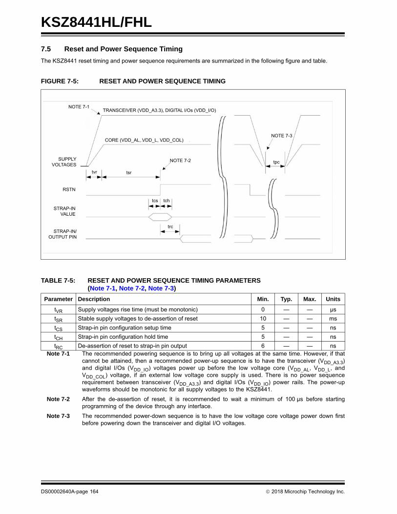
KSZ8441HL/FHL
7.5 Reset and Power Sequence Timing
The KSZ8441 reset timing and power sequence requirements are summarized in the following figure and table.
Note 7-1 The recommended powering sequence is to bring up all voltages at the same time. However, if thatcannot be attained, then a recommended power-up sequence is to have the transceiver (VDD_A3.3)and digital I/Os (VDD_IO) voltages power up before the low voltage core (VDD_AL, VDD_L, andVDD_COL) voltage, if an external low voltage core supply is used. There is no power sequencerequirement between transceiver (VDD_A3.3) and digital I/Os (VDD_IO) power rails. The power-upwaveforms should be monotonic for all supply voltages to the KSZ8441.
Note 7-2 After the de-assertion of reset, it is recommended to wait a minimum of 100 μs before startingprogramming of the device through any interface.
Note 7-3 The recommended power-down sequence is to have the low voltage core voltage power down firstbefore powering down the transceiver and digital I/O voltages.
FIGURE 7-5: RESET AND POWER SEQUENCE TIMING
TABLE 7-5: RESET AND POWER SEQUENCE TIMING PARAMETERS (Note 7-1, Note 7-2, Note 7-3)
Parameter Description Min. Typ. Max. Units
tVR Supply voltages rise time (must be monotonic) 0 — — µs
tSR Stable supply voltages to de-assertion of reset 10 — — ms
tCS Strap-in pin configuration setup time 5 — — ns
tCH Strap-in pin configuration hold time 5 — — ns
tRC De-assertion of reset to strap-in pin output 6 — — ns
TRANSCEIVER (VDD_A3.3), DIGITAL I/Os (VDD_I/O)
CORE (VDD_AL, VDD_L, VDD_COL)
tpc
tvr tsr
tcs tch
trc
SUPPLYVOLTAGES
RSTN
STRAP-INVALUE
STRAP-IN/OUTPUT PIN
NOTE 7-1
NOTE 7-2
NOTE 7-3
DS00002640A-page 164 2018 Microchip Technology Inc.

KSZ8441HL/FHL
7.6 Reset Circuit Guidelines
The following reset circuit is recommended for powering up the KSZ8441 device if reset is triggered by the power supply.
The following reset circuit is recommended for applications where reset is driven by another device (e.g., CPU orFPGA). At POR, R, C, and D1 provide the necessary ramp rise time to reset the KSZ8441 device. The RST_OUT_Nfrom CPU/FPGA provides the warm reset after power-up.
FIGURE 7-6: SIMPLE RESET CIRCUIT
FIGURE 7-7: RECOMMENDED RESET CIRCUIT FOR INTERFACING WITH CPU/FPGA RESET OUTPUT
VDD_IO
D1 R 10KKSZ8441
RSTN
C 10μF
D1: 1N4148
VDD_IO
D1 R 10KKSZ8441
RSTN
C 10μFD2
D1, D2: 1N4148
CPU/FPGA
RST_OUT_N
2018 Microchip Technology Inc. DS00002640A-page 165

KSZ8441HL/FHL
8.0 REFERENCE CIRCUIT: LED STRAP-IN PINS
The pull-up and pull-down reference circuits for the P1LED0/H816 strapping pin are shown in Figure 8-1.
The supply voltage for the LEDs must be at least ~2.2V, depending on the particular LED and the load resistor. IfVDD_IO is 1.8V, then a different (higher voltage) supply must be used for the LEDs.
FIGURE 8-1: TYPICAL LED STRAP-IN CIRCUIT
LED PIN
10 220
220
VDD_IO
1k FOR VDD_IO = 2.5V500 ~ 700 FOR VDD_IO = 3.3V
PULL-UP
KSZ8441
VDD_IO
PULL-DOWN
KSZ8441LED PIN
DS00002640A-page 166 2018 Microchip Technology Inc.
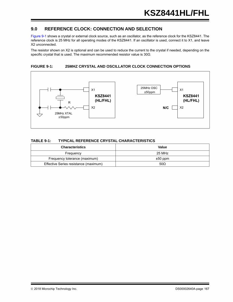
KSZ8441HL/FHL
9.0 REFERENCE CLOCK: CONNECTION AND SELECTION
Figure 9-1 shows a crystal or external clock source, such as an oscillator, as the reference clock for the KSZ8441. Thereference clock is 25 MHz for all operating modes of the KSZ8441. If an oscillator is used, connect it to X1, and leaveX2 unconnected.
The resistor shown on X2 is optional and can be used to reduce the current to the crystal if needed, depending on thespecific crystal that is used. The maximum recommended resistor value is 30Ω.
FIGURE 9-1: 25MHZ CRYSTAL AND OSCILLATOR CLOCK CONNECTION OPTIONS
TABLE 9-1: TYPICAL REFERENCE CRYSTAL CHARACTERISTICS
Characteristics Value
Frequency 25 MHz
Frequency tolerance (maximum) ±50 ppm
Effective Series resistance (maximum) 50Ω
KSZ8441 (HL/FHL)
X1
X2
KSZ8441 (HL/FHL)
X1
X2
25 MHz OSC 50 ppm
N/CR
25 MHz XTAL± 50 ppm
±
2018 Microchip Technology Inc. DS00002640A-page 167

KSZ8441HL/FHL
10.0 SELECTION OF ISOLATION TRANSFORMERS
A 1:1 isolation transformer is required at the line interface. An isolation transformer with integrated common-mode chokeis recommended for exceeding FCC requirements.
Table 10-1 lists recommended transformer characteristics.
TABLE 10-1: TRANSFORMER SELECTION CRITERIA
Parameter Value Test Conditions
Turns Ratio 1 CT:1 CT —
Open-Circuit Inductance (min.) 350 µH 100 mV, 100 kHz, 8 mA
Leakage Inductance (max.) 0.4 µH 1 MHz (min.)
Interwinding Capacitance (max.) 12 pF —
D.C. Resistance (max.) 0.9Ω —
Insertion Loss (max.) –1.0 dB 100 kHz to 100 MHz
HIPOT (min.) 1500 VRMS —
TABLE 10-2: QUALIFIED SINGLE-PORT MAGNETICS
Manufacturer Part Number Auto MDI-X
Pulse H1102NL Yes
Pulse (low cost) H1260 Yes
Transpower HB726 Yes
Bel Fuse S558-5999-U7 Yes
Delta LF8505 Yes
LanKom LF-H41S Yes
TDK (Mag Jack) TLA-6T718 Yes
DS00002640A-page 168 2018 Microchip Technology Inc.
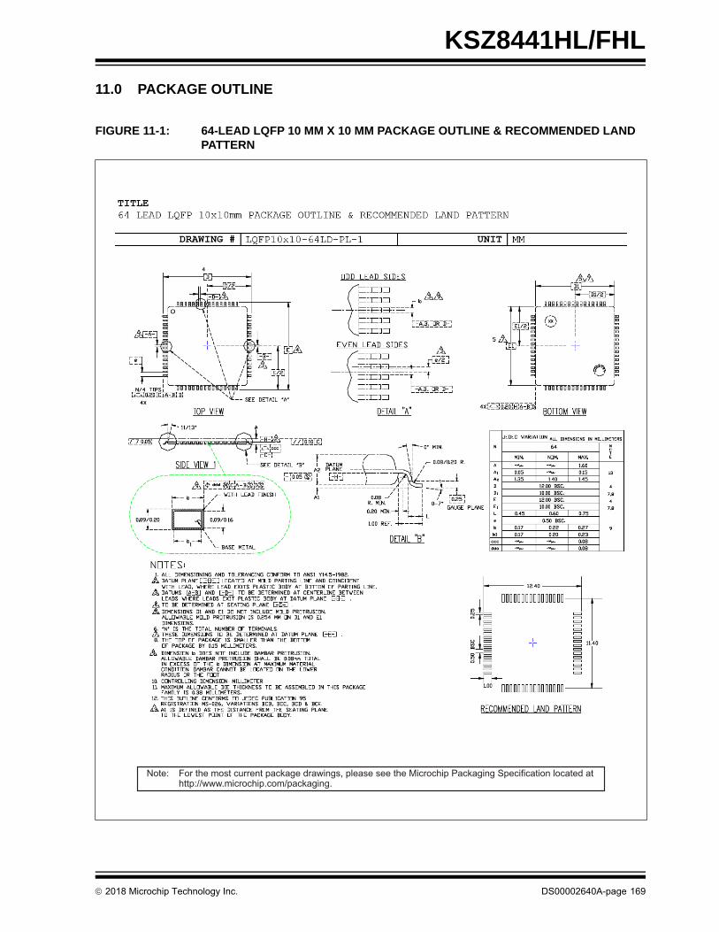
2018 Microchip Technology Inc. DS00002640A-page 169
KSZ8441HL/FHL
11.0 PACKAGE OUTLINE
FIGURE 11-1: 64-LEAD LQFP 10 MM X 10 MM PACKAGE OUTLINE & RECOMMENDED LAND PATTERN
Note: For the most current package drawings, please see the Microchip Packaging Specification located at http://www.microchip.com/packaging.

KSZ8441HL/FHL
DS00002640A-page 170 2018 Microchip Technology Inc.
APPENDIX A: DATA SHEET REVISION HISTORY
TABLE A-1: REVISION HISTORY
Revision Section/Figure/Entry Correction
DS00002640A (2-22-18) —Converted Micrel data sheet KSZ8441HL/FHL to Microchip DS00002640A. Minor text changes throughout.

2018 Microchip Technology Inc. DS00002640A-page 171
KSZ8441HL/FHL
THE MICROCHIP WEB SITE
Microchip provides online support via our WWW site at www.microchip.com. This web site is used as a means to makefiles and information easily available to customers. Accessible by using your favorite Internet browser, the web site con-tains the following information:
• Product Support – Data sheets and errata, application notes and sample programs, design resources, user’s guides and hardware support documents, latest software releases and archived software
• General Technical Support – Frequently Asked Questions (FAQ), technical support requests, online discussion groups, Microchip consultant program member listing
• Business of Microchip – Product selector and ordering guides, latest Microchip press releases, listing of semi-nars and events, listings of Microchip sales offices, distributors and factory representatives
CUSTOMER CHANGE NOTIFICATION SERVICE
Microchip’s customer notification service helps keep customers current on Microchip products. Subscribers will receivee-mail notification whenever there are changes, updates, revisions or errata related to a specified product family ordevelopment tool of interest.
To register, access the Microchip web site at www.microchip.com. Under “Support”, click on “Customer Change Notifi-cation” and follow the registration instructions.
CUSTOMER SUPPORT
Users of Microchip products can receive assistance through several channels:
• Distributor or Representative
• Local Sales Office
• Field Application Engineer (FAE)
• Technical Support
Customers should contact their distributor, representative or field application engineer (FAE) for support. Local salesoffices are also available to help customers. A listing of sales offices and locations is included in the back of this docu-ment.
Technical support is available through the web site at: http://microchip.com/support

KSZ8441HL/FHL
DS00002640A-page 172 2018 Microchip Technology Inc.
PRODUCT IDENTIFICATION SYSTEM
To order or obtain information, e.g., on pricing or delivery, refer to the factory or the listed sales office.
Device: KSZ8441
Interface: H = Generic Host Bus InterfaceFH = Generic Host Bus Interface with Fiber support
Package: L = 64-Lead LQFP
Temperature: I = –40C to +85C (Industrial)
Media Type: <blank> = 160/Tray
Examples:
a) KSZ8441HLI: Generic Host Bus Interface, 64-Lead LQFP,Industrial Temperature, 160/Tray
b) KSZ8441FHLI: Generic Host Bus Interface with Fiber Support, 64-Lead LQFP,Industrial Temperature, 160/Tray
PART NO. X X
PackageInterfaceDevice
X
Temperature
XX
MediaType
2018 Microchip Technology Inc. DS00002640A-page 173
Information contained in this publication regarding device applications and the like is provided only for your convenience and may besuperseded by updates. It is your responsibility to ensure that your application meets with your specifications. MICROCHIP MAKES NOREPRESENTATIONS OR WARRANTIES OF ANY KIND WHETHER EXPRESS OR IMPLIED, WRITTEN OR ORAL, STATUTORY OROTHERWISE, RELATED TO THE INFORMATION, INCLUDING BUT NOT LIMITED TO ITS CONDITION, QUALITY, PERFORMANCE,MERCHANTABILITY OR FITNESS FOR PURPOSE. Microchip disclaims all liability arising from this information and its use. Use ofMicrochip devices in life support and/or safety applications is entirely at the buyer’s risk, and the buyer agrees to defend, indemnify andhold harmless Microchip from any and all damages, claims, suits, or expenses resulting from such use. No licenses are conveyed, implic-itly or otherwise, under any Microchip intellectual property rights unless otherwise stated.
Trademarks
The Microchip name and logo, the Microchip logo, AnyRate, AVR, AVR logo, AVR Freaks, BeaconThings, BitCloud, CryptoMemory, CryptoRF, dsPIC, FlashFlex, flexPWR, Heldo, JukeBlox, KEELOQ, KEELOQ logo, Kleer, LANCheck, LINK MD, maXStylus, maXTouch, MediaLB, megaAVR, MOST, MOST logo, MPLAB, OptoLyzer, PIC, picoPower, PICSTART, PIC32 logo, Prochip Designer, QTouch, RightTouch, SAM-BA, SpyNIC, SST, SST Logo, SuperFlash, tinyAVR, UNI/O, and XMEGA are registered trademarks of Microchip Technology Incorporated in the U.S.A. and other countries.
ClockWorks, The Embedded Control Solutions Company, EtherSynch, Hyper Speed Control, HyperLight Load, IntelliMOS, mTouch, Precision Edge, and Quiet-Wire are registered trademarks of Microchip Technology Incorporated in the U.S.A.
Adjacent Key Suppression, AKS, Analog-for-the-Digital Age, Any Capacitor, AnyIn, AnyOut, BodyCom, chipKIT, chipKIT logo, CodeGuard, CryptoAuthentication, CryptoCompanion, CryptoController, dsPICDEM, dsPICDEM.net, Dynamic Average Matching, DAM, ECAN, EtherGREEN, In-Circuit Serial Programming, ICSP, Inter-Chip Connectivity, JitterBlocker, KleerNet, KleerNet logo, Mindi, MiWi, motorBench, MPASM, MPF, MPLAB Certified logo, MPLIB, MPLINK, MultiTRAK, NetDetach, Omniscient Code Generation, PICDEM, PICDEM.net, PICkit, PICtail, PureSilicon, QMatrix, RightTouch logo, REAL ICE, Ripple Blocker, SAM-ICE, Serial Quad I/O, SMART-I.S., SQI, SuperSwitcher, SuperSwitcher II, Total Endurance, TSHARC, USBCheck, VariSense, ViewSpan, WiperLock, Wireless DNA, and ZENA are trademarks of Microchip Technology Incorporated in the U.S.A. and other countries.
SQTP is a service mark of Microchip Technology Incorporated in the U.S.A.
Silicon Storage Technology is a registered trademark of Microchip Technology Inc. in other countries.
GestIC is a registered trademark of Microchip Technology Germany II GmbH & Co. KG, a subsidiary of Microchip Technology Inc., in other countries.
All other trademarks mentioned herein are property of their respective companies.
© 2018, Microchip Technology Incorporated, All Rights Reserved.
ISBN: 978-1-5224-2708-7
Note the following details of the code protection feature on Microchip devices:
• Microchip products meet the specification contained in their particular Microchip Data Sheet.
• Microchip believes that its family of products is one of the most secure families of its kind on the market today, when used in the intended manner and under normal conditions.
• There are dishonest and possibly illegal methods used to breach the code protection feature. All of these methods, to our knowledge, require using the Microchip products in a manner outside the operating specifications contained in Microchip’s Data Sheets. Most likely, the person doing so is engaged in theft of intellectual property.
• Microchip is willing to work with the customer who is concerned about the integrity of their code.
• Neither Microchip nor any other semiconductor manufacturer can guarantee the security of their code. Code protection does not mean that we are guaranteeing the product as “unbreakable.”
Code protection is constantly evolving. We at Microchip are committed to continuously improving the code protection features of ourproducts. Attempts to break Microchip’s code protection feature may be a violation of the Digital Millennium Copyright Act. If such actsallow unauthorized access to your software or other copyrighted work, you may have a right to sue for relief under that Act.
Microchip received ISO/TS-16949:2009 certification for its worldwide headquarters, design and wafer fabrication facilities in Chandler and Tempe, Arizona; Gresham, Oregon and design centers in California and India. The Company’s quality system processes and procedures are for its PIC® MCUs and dsPIC® DSCs, KEELOQ® code hopping devices, Serial EEPROMs, microperipherals, nonvolatile memory and analog products. In addition, Microchip’s quality system for the design and manufacture of development systems is ISO 9001:2000 certified.
QUALITYMANAGEMENTSYSTEMCERTIFIEDBYDNV
== ISO/TS16949==

DS00002640A-page 174 2018 Microchip Technology Inc.
NOTES:

DS00002640A-page 175 2018 Microchip Technology Inc.
AMERICASCorporate Office2355 West Chandler Blvd.Chandler, AZ 85224-6199Tel: 480-792-7200 Fax: 480-792-7277Technical Support: http://www.microchip.com/supportWeb Address: www.microchip.com
AtlantaDuluth, GA Tel: 678-957-9614 Fax: 678-957-1455
Austin, TXTel: 512-257-3370
BostonWestborough, MA Tel: 774-760-0087 Fax: 774-760-0088
ChicagoItasca, IL Tel: 630-285-0071 Fax: 630-285-0075
DallasAddison, TX Tel: 972-818-7423 Fax: 972-818-2924
DetroitNovi, MI Tel: 248-848-4000
Houston, TX Tel: 281-894-5983
IndianapolisNoblesville, IN Tel: 317-773-8323Fax: 317-773-5453Tel: 317-536-2380
Los AngelesMission Viejo, CA Tel: 949-462-9523Fax: 949-462-9608Tel: 951-273-7800
Raleigh, NC Tel: 919-844-7510
New York, NY Tel: 631-435-6000
San Jose, CA Tel: 408-735-9110Tel: 408-436-4270
Canada - TorontoTel: 905-695-1980 Fax: 905-695-2078
ASIA/PACIFICAustralia - SydneyTel: 61-2-9868-6733
China - BeijingTel: 86-10-8569-7000
China - ChengduTel: 86-28-8665-5511
China - ChongqingTel: 86-23-8980-9588
China - DongguanTel: 86-769-8702-9880
China - GuangzhouTel: 86-20-8755-8029
China - HangzhouTel: 86-571-8792-8115
China - Hong Kong SARTel: 852-2943-5100
China - NanjingTel: 86-25-8473-2460
China - QingdaoTel: 86-532-8502-7355
China - ShanghaiTel: 86-21-3326-8000
China - ShenyangTel: 86-24-2334-2829
China - ShenzhenTel: 86-755-8864-2200
China - SuzhouTel: 86-186-6233-1526
China - WuhanTel: 86-27-5980-5300
China - XianTel: 86-29-8833-7252
China - XiamenTel: 86-592-2388138
China - ZhuhaiTel: 86-756-3210040
ASIA/PACIFICIndia - BangaloreTel: 91-80-3090-4444
India - New DelhiTel: 91-11-4160-8631
India - PuneTel: 91-20-4121-0141
Japan - OsakaTel: 81-6-6152-7160
Japan - TokyoTel: 81-3-6880- 3770
Korea - DaeguTel: 82-53-744-4301
Korea - SeoulTel: 82-2-554-7200
Malaysia - Kuala LumpurTel: 60-3-7651-7906
Malaysia - PenangTel: 60-4-227-8870
Philippines - ManilaTel: 63-2-634-9065
SingaporeTel: 65-6334-8870
Taiwan - Hsin ChuTel: 886-3-577-8366
Taiwan - KaohsiungTel: 886-7-213-7830
Taiwan - TaipeiTel: 886-2-2508-8600
Thailand - BangkokTel: 66-2-694-1351
Vietnam - Ho Chi MinhTel: 84-28-5448-2100
EUROPEAustria - WelsTel: 43-7242-2244-39Fax: 43-7242-2244-393
Denmark - CopenhagenTel: 45-4450-2828 Fax: 45-4485-2829
Finland - EspooTel: 358-9-4520-820
France - ParisTel: 33-1-69-53-63-20 Fax: 33-1-69-30-90-79
Germany - GarchingTel: 49-8931-9700
Germany - HaanTel: 49-2129-3766400
Germany - HeilbronnTel: 49-7131-67-3636
Germany - KarlsruheTel: 49-721-625370
Germany - MunichTel: 49-89-627-144-0 Fax: 49-89-627-144-44
Germany - RosenheimTel: 49-8031-354-560
Israel - Ra’anana Tel: 972-9-744-7705
Italy - Milan Tel: 39-0331-742611 Fax: 39-0331-466781
Italy - PadovaTel: 39-049-7625286
Netherlands - DrunenTel: 31-416-690399 Fax: 31-416-690340
Norway - TrondheimTel: 47-7289-7561
Poland - WarsawTel: 48-22-3325737
Romania - BucharestTel: 40-21-407-87-50
Spain - MadridTel: 34-91-708-08-90Fax: 34-91-708-08-91
Sweden - GothenbergTel: 46-31-704-60-40
Sweden - StockholmTel: 46-8-5090-4654
UK - WokinghamTel: 44-118-921-5800Fax: 44-118-921-5820
Worldwide Sales and Service
10/25/17