Embed Size (px)
Citation preview

STATUS OF THESIS
Title of thesis NEGATIVE BIAS TEMPERATURE INSTABILITY STUDIES
FOR ANALOG SOC CIRCUITS
I MOHD AZMAN ABDUL LATIF
hereby allow my thesis to be placed at the Information Resource Center (IRC) ofUniversiti Teknologi PETRONAS (UTP) with the following conditions:
1. The thesis becomes the property of UTP
2. The IRC of UTP may make copies of the thesis for academic purposes only.
3. This thesis is classified as
Confidential
Non-confidential
If this thesis is confidential, please state the reason:
The contents of the thesis will remain confidential for years.
Remarks on disclosure:
Endorsed by:
Signature of Author
Permanent Address:4,Persiaran Seksyen 2/15,Bandar Putra Bertam,13200 K. Batas, Penang, Malaysia
Signature of Supervisor
Name of Supervisor:Dr. Noohul Basheer Zain Ali
Date: Date:

UNIVERSITI TEKNOLOGI PETRONAS
NEGATIVE BIAS TEMPERATURE INSTABILITY STUDIES FOR ANALOG SOC
CIRCUITS
by
MOHD AZMAN ABDUL LATIF
The undersigned certify that they have read, and recommend to the Postgraduate
Studies Programme for acceptance of this thesis for the fulfilment of the requirements
for the degree stated.
Signature:
Main Supervisor: Dr. Noohul Basheer Zain Ali
Signature:
Co-Supervisor: Dr. Fawnizu Azmadi Hussin
Signature:
Head of Department: Assoc. Prof. Dr. Nor Hisham Hamid
Date:

NEGATIVE BIAS TEMPERATURE INSTABILITY STUDIES FOR ANALOG SOC
CIRCUITS
by
MOHD AZMAN ABDUL LATIF
A Thesis
Submitted to the Postgraduate Studies Programme
as a Requirement for the Degree of
MASTER OF SCIENCE
ELECTRICAL & ELECTRONIC ENGINEERING DEPARTMENT
UNIVERSITI TEKNOLOGI PETRONAS
BANDAR SERI ISKANDAR
PERAK
MARCH 2012

DECLARATION OF THESIS
Title of thesis NEGATIVE BIAS TEMPERATURE INSTABILITY STUDIES
FOR ANALOG SOC CIRCUITS
I MOHD AZMAN ABDUL LATIF
hereby declare that the thesis is based on my original work except for quotations andcitations which have been duly acknowledged. I also declare that it has not been previ-ously or concurrently submitted for any other degree at UTP or other institutions.
Witnessed by
Signature of Author
Permanent Address:4,Persiaran Seksyen 2/15,Bandar Putra Bertam,13200 K. Batas, Penang, Malaysia
Signature of Supervisor
Name of Supervisor:Dr. Noohul Basheer Zain Ali
Date: Date:
iv
In compliance with the terms of the Copyright Act 1987 and the IP Policy of theuniversity, the copyright of this thesis has been reassigned by the author to the legalentity of the university,
Institute of Technology PETRONAS Sdn Bhd.
Due acknowledgement shall always be made of the use of any material contained in, orderived from, this thesis.
c©Mohd Azman Abdul Latif, 2012Institute of Technology PETRONAS Sdn BhdAll rights reserved.
v

ACKNOWLEDGEMENTS
First, I am grateful to my University advisor, Dr. Noohul Basheer Zain Ali, and my
co-advisor, Dr. Fawnizu Azmadi Hussin, for their unwavering support and guidance
over the last one and a half years throughout my graduate studies. Their insightful
knowledge, comments and wisdom have proved to be invaluable to the completion of
my Msc. degree and this thesis. I would like to thank Kevin Arendt of Intel Corporation
for providing the thermal sensor circuit and extensive experience on analog circuits
particularly the bandgap reference and for providing the sample circuits and reliability
data used in this paper. This work is dedicated to my caring, loving and supportive wife,
Dr. Ismaliza Ismail. Without her I could not have finished this journey and completed
this thesis on a part time basis within one and a half years. Her genuine encouragement
and understanding over the years have been invaluable. I would also like to thank the
rest of my immediate and extended family for their emotional support throughout my
graduate studies.
vi

ABSTRACT
Negative Bias Temperature Instability (NBTI) is one of the recent reliability issues in
subthreshold CMOS circuits. NBTI effect on analog circuits, which require matched
device pairs and mismatches, will cause circuit failure. This work is to assess the NBTI
effect considering the voltage and the temperature variations. It also provides a working
knowledge of NBTI awareness to the circuit design community for reliable design of
the SOC analog circuit. There has been numerous studies to date on the NBTI effect to
analog circuits. However, other researchers did not study the implication of NBTI stress
on analog circuits utilizing bandgap reference circuit. The reliability performance of all
matched pair circuits, particularly the bandgap reference, is at the mercy of aging differ-
ential. Reliability simulation is mandatory to obtain realistic risk evaluation for circuit
design reliability qualification. It is applicable to all circuit aging problems covering
both analog and digital. Failure rate varies as a function of voltage and temperature.
It is shown that PMOS is the reliability-susceptible device and NBTI is the most vital
failure mechanism for analog circuit in sub-micrometer CMOS technology. This study
provides a complete reliability simulation analysis of the on-die Thermal Sensor and
the Digital Analog Converter (DAC) circuits and analyze the effect of NBTI using reli-
ability simulation tool. In order to checkout the robustness of the NBTI-induced SOC
circuit design,a burn-in experiment was conducted on the DAC circuits. The NBTI
degradation observed in the reliability simulation analysis has given a clue that under
a severe stress condition, a significant voltage threshold mismatch of beyond the 2mV
limit was recorded. Burn-in experimental result on DAC confirms the reliability sensi-
tivity of NBTI to the DAC circuit design.
vii

ABSTRAK
Suhu Bias Negatif Ketakstabilan (NBTI) adalah salah satu isu keboleharapan terkini
dalam litar CMOS ambang sub. Kesan NBTI pada litar analog, yang memerlukan
pasangan dan ketidakpadanan peranti dipadankan, akan menyebabkan kegagalan litar.
Kerja ini adalah untuk menilai kesan NBTI khususnya voltan dan suhu. Ia juga menye-
diakan pengetahuan kerja NBTI kesedaran kepada masyarakat reka bentuk litar untuk
reka bentuk dipercayai litar analog SOC. Terdapat banyak kajian sehingga kini berke-
naan dengan kesan NBTI litar analog. Walau bagaimanapun, penyelidik lain tidak
mengkaji implikasi tekanan NBTI atas litar analog yang menggunakan litar rujukan
bandgap. Prestasi keboleharapan semua litar pasangan yang sepadan, khususnya ru-
jukan bandgap, pada rahmat penuaan kebezaan. Simulasi Keboleharapan adalah wa-
jib untuk mendapatkan penilaian risiko yang realistik untuk reka bentuk kebolehara-
pan kelayakan litar. Ianya menyebabkan kepada litar semua penuaan masalah yang
merangkumi kedua-dua analog dan digital. Kadar kegagalan berbeza-beza sebagai
fungsi voltan dan suhu. Ia menunjukkan bahawa PMOS peranti mudah terpengaruh
kebolehpercayaan dan NBTI mekanisme kegagalan yang paling penting untuk litar
analog dalam sub-mikrometer teknologi CMOS. Kajian ini menyediakan simulasi ke-
boleharapan analisis lengkap Sensor terma-mati dan Penukar Analog Digital (DAC)
litar dan menganalisis kesan NBTI menggunakan keboleharapan alat simulasi. Dalam
usaha menguji keteguhan reka bentuk NBTI yang disebabkan oleh litar SOC, per-
cubaan membakar dalam telah dijalankan ke atas litar DAC. Kemerosotan NBTI yang
diperhatikan dalam analisis simulasi keboleharapan telah memberi petunjuk bahawa di
bawah keadaan tekanan yang teruk, voltan yang signifikan ambang ketidaksepadanan
yang melebihi had 2mV dicatatkan. Membakar dalam keputusan uji kaji pada DAC
mengesahkan sensitiviti kebolehpercayaan NBTI kepada reka bentuk litar DAC.
viii

TABLE OF CONTENTS
Acknowledgements . . . . . . . . . . . . . . . . . . . . . . . . . . . . . . . . . vi
Abstract . . . . . . . . . . . . . . . . . . . . . . . . . . . . . . . . . . . . . . . vii
Abstrak . . . . . . . . . . . . . . . . . . . . . . . . . . . . . . . . . . . . . . . viii
Chapter
1 Introduction . . . . . . . . . . . . . . . . . . . . . . . . . . . . . . . . . . . 1
1.1 Background . . . . . . . . . . . . . . . . . . . . . . . . . . . . . . . . 1
1.2 Thesis Objectives . . . . . . . . . . . . . . . . . . . . . . . . . . . . . 3
1.3 Thesis Outline . . . . . . . . . . . . . . . . . . . . . . . . . . . . . . . 4
2 Reliability Modeling, Mechanisms and Stresses . . . . . . . . . . . . . . . . 7
2.1 Reliability Modeling for Analog Circuit Design . . . . . . . . . . . . . 7
2.2 Failure Mechanisms . . . . . . . . . . . . . . . . . . . . . . . . . . . . 9
2.2.1 Negative Bias Temperature Instability (NBTI) . . . . . . . . . . 9
2.2.1.1 NBTI Origin . . . . . . . . . . . . . . . . . . . . . . 10
2.2.2 Other CMOS Defect Models . . . . . . . . . . . . . . . . . . . 15
2.2.2.1 Time Dependant Dielectric Breakdown (TDDB) . . . 15
2.2.2.2 Hot Carrier Injection (HCI) . . . . . . . . . . . . . . 16
2.3 Burn-In Stress Test . . . . . . . . . . . . . . . . . . . . . . . . . . . . 16
2.3.1 Introduction . . . . . . . . . . . . . . . . . . . . . . . . . . . . 16
2.3.2 Analog versus Digital Burn-In . . . . . . . . . . . . . . . . . . 19
2.3.3 Wafer Level Burn-In stress (WLBI) . . . . . . . . . . . . . . . 20
2.3.4 High Temperature Operation Life (HTOL) . . . . . . . . . . . . 20
2.4 Summary . . . . . . . . . . . . . . . . . . . . . . . . . . . . . . . . . 21
3 Bandgap Reference and its applications . . . . . . . . . . . . . . . . . . . . 23
3.1 Bandgap Reference Circuit . . . . . . . . . . . . . . . . . . . . . . . . 23
ix

3.2 Key applications utilizing Bandgap reference in SOC Design . . . . . . 25
3.2.1 DAC Circuit . . . . . . . . . . . . . . . . . . . . . . . . . . . . 26
3.2.1.1 Output Voltage Compliance . . . . . . . . . . . . . . 27
3.2.1.2 Output Current . . . . . . . . . . . . . . . . . . . . . 27
3.2.1.3 DAC Resolution and Accuracy . . . . . . . . . . . . . 28
3.2.1.4 Full Scale Error . . . . . . . . . . . . . . . . . . . . 29
3.2.1.5 DAC Linearity (INL / DNL) . . . . . . . . . . . . . . 31
3.2.2 ADC circuit . . . . . . . . . . . . . . . . . . . . . . . . . . . . 32
3.2.3 PLL Circuit . . . . . . . . . . . . . . . . . . . . . . . . . . . . 33
3.2.4 Thermal Sensor Circuit . . . . . . . . . . . . . . . . . . . . . . 35
3.3 Sources of error in bandgap reference . . . . . . . . . . . . . . . . . . 36
3.3.1 Mismatch in current mirror . . . . . . . . . . . . . . . . . . . . 37
3.3.2 Mismatch in resistor . . . . . . . . . . . . . . . . . . . . . . . 37
3.3.3 Mismatch in resistor tolerance . . . . . . . . . . . . . . . . . . 37
3.3.4 Mismatch in operational amplifier . . . . . . . . . . . . . . . . 38
3.3.5 Mismatch in diodes . . . . . . . . . . . . . . . . . . . . . . . . 38
3.4 Summary . . . . . . . . . . . . . . . . . . . . . . . . . . . . . . . . . 39
4 Reliability Simulation . . . . . . . . . . . . . . . . . . . . . . . . . . . . . 41
4.1 Introduction . . . . . . . . . . . . . . . . . . . . . . . . . . . . . . . . 41
4.2 Choice of Reliability Simulator . . . . . . . . . . . . . . . . . . . . . . 42
4.3 Methodology . . . . . . . . . . . . . . . . . . . . . . . . . . . . . . . 45
4.3.1 Assumptions of the reliability simulation model . . . . . . . . . 48
4.3.2 Stress Mode . . . . . . . . . . . . . . . . . . . . . . . . . . . . 50
4.3.3 Playback Mode . . . . . . . . . . . . . . . . . . . . . . . . . . 50
4.4 Case Study 1 : On-Die Thermal Sensor Reliability Prediction . . . . . . 51
4.4.1 On-Die Thermal Sensor Design . . . . . . . . . . . . . . . . . 51
4.4.2 AgingSim Process Step . . . . . . . . . . . . . . . . . . . . . . 55
4.4.3 Voltage Sensitivity Analysis . . . . . . . . . . . . . . . . . . . 58
4.4.4 Temperature Sensitivity Analysis . . . . . . . . . . . . . . . . . 59
4.5 Case Study 2 : Digital Analog Converter Reliability Prediction . . . . . 61
4.5.1 Digital Analog Converter Design . . . . . . . . . . . . . . . . . 62
x

4.5.2 AgingSim Process Flow . . . . . . . . . . . . . . . . . . . . . 63
4.5.3 DAC Circuit Design . . . . . . . . . . . . . . . . . . . . . . . . 65
4.5.4 Voltage Sensitivity Analysis . . . . . . . . . . . . . . . . . . . 68
4.5.5 Temperature Sensitivity Analysis . . . . . . . . . . . . . . . . . 69
4.6 Summary . . . . . . . . . . . . . . . . . . . . . . . . . . . . . . . . . 70
5 Burn-In Stress on Digital-Analog-Converter (DAC) . . . . . . . . . . . . . . 73
5.1 Introduction . . . . . . . . . . . . . . . . . . . . . . . . . . . . . . . . 73
5.2 DAC Burn-In Conditions . . . . . . . . . . . . . . . . . . . . . . . . . 75
5.3 DAC Burn-In Stress Test Mode . . . . . . . . . . . . . . . . . . . . . . 76
5.4 Burn-In System . . . . . . . . . . . . . . . . . . . . . . . . . . . . . . 78
5.5 DAC Burn-In Experiment . . . . . . . . . . . . . . . . . . . . . . . . . 79
5.6 DAC Burn-In Result . . . . . . . . . . . . . . . . . . . . . . . . . . . . 82
5.7 Correlation of Simulation and Experimental Work . . . . . . . . . . . . 86
5.8 Summary . . . . . . . . . . . . . . . . . . . . . . . . . . . . . . . . . 87
6 Conclusions and future work . . . . . . . . . . . . . . . . . . . . . . . . . . 89
6.1 Conclusion . . . . . . . . . . . . . . . . . . . . . . . . . . . . . . . . 89
6.1.1 Voltage and temperature variation in NBTI Model for Circuit
Design . . . . . . . . . . . . . . . . . . . . . . . . . . . . . . . 90
6.1.2 A special Burn In experiment looking into NBTI reliability sen-
sitivity . . . . . . . . . . . . . . . . . . . . . . . . . . . . . . . 90
6.2 Future Work . . . . . . . . . . . . . . . . . . . . . . . . . . . . . . . . 92
xi

LIST OF TABLES
4.1 Comparison of various reliability simulators [1, 2]. . . . . . . . . . . . 43
4.2 AgingSim Settings across 3 different modes. . . . . . . . . . . . . . . . 57
4.3 AgingSim - Post Stress Result. . . . . . . . . . . . . . . . . . . . . . . 57
4.4 Matched devices in Op Amp. . . . . . . . . . . . . . . . . . . . . . . . 57
4.5 AgingSim parameters across three different conditions . . . . . . . . . 65
4.6 AgingSim result comparing current source/differential pairs at 3.3V and
4.6V . . . . . . . . . . . . . . . . . . . . . . . . . . . . . . . . . . . . 68
5.1 Calculated acceleration factors. . . . . . . . . . . . . . . . . . . . . . . 77
5.2 Summary of 168 hours (7 years) Burn-In experiment of DAC . . . . . . 83
5.3 The Vout data taken before and after Burn-In stress . . . . . . . . . . . 84
xii

LIST OF FIGURES
2.1 CMOS Inverter Voltage Waveforms . . . . . . . . . . . . . . . . . . . 11
2.2 Schematic description of the NBTI event (left) and possible mechanism
for breaking interfacial Si-H bonds by inversion-layer holes (right). . . . 12
2.3 NBTI trend increases as the technology nodes goes with the narrower
channel length [3] . . . . . . . . . . . . . . . . . . . . . . . . . . . . . 12
2.4 PMOS Stress Modes . . . . . . . . . . . . . . . . . . . . . . . . . . . 14
2.5 Bathtub curve . . . . . . . . . . . . . . . . . . . . . . . . . . . . . . . 18
2.6 Typical manufacturing production flow . . . . . . . . . . . . . . . . . . 19
3.1 Basic CMOS Bandgap Reference Circuit. . . . . . . . . . . . . . . . . 25
3.2 Architecture and techology comparisons of various DAC selections. . . 27
3.3 4-Bit DAC Offset error transfer function. . . . . . . . . . . . . . . . . . 30
3.4 4-Bit DAC Gain Error transfer function. . . . . . . . . . . . . . . . . . 31
3.5 Examples of DNL and INL transfer funtion. . . . . . . . . . . . . . . . 32
3.6 Bandgap reference usage on PLL design. . . . . . . . . . . . . . . . . . 34
3.7 Bandgap reference sources of error. . . . . . . . . . . . . . . . . . . . . 36
4.1 Reliability simulation flow . . . . . . . . . . . . . . . . . . . . . . . . 44
4.2 NBTI periodic stress and relaxation [4]. . . . . . . . . . . . . . . . . . 48
4.3 Thermal Sensor Block Diagram. . . . . . . . . . . . . . . . . . . . . . 52
4.4 AgingSim Voltage variations. . . . . . . . . . . . . . . . . . . . . . . . 59
4.5 Lifetime as a function as temperature [5]. . . . . . . . . . . . . . . . . 59
4.6 AgingSim considering temperature variation. . . . . . . . . . . . . . . 60
4.7 The 8-bit CRT DAC block diagram. . . . . . . . . . . . . . . . . . . . 62
4.8 Simplified circuit diagram of 8-bit CRT DAC [1]. . . . . . . . . . . . . 64
xiii

4.9 Circuit diagram of the current source/differential switch for the CRT
DAC [1]. . . . . . . . . . . . . . . . . . . . . . . . . . . . . . . . . . . 66
4.10 Threshold voltage variation as a function of operational time . . . . . . 69
4.11 Temperature variation as a function of Vccmax . . . . . . . . . . . . . 70
5.1 The pulse width of the status signal of the Burn-In monitor output pin. . 78
5.2 DAC Burn-In Experimental Flow. . . . . . . . . . . . . . . . . . . . . 81
5.3 DAC burn-in comparison, 3.3V vs 4.6V . . . . . . . . . . . . . . . . . 82
5.4 Lifetime as a function of gate voltage. Data after Schroder et al.[5]. . . 83
5.5 DAC characteristic showing an excessive gain error of 43.5% . . . . . . 85
5.6 DAC Output signal during burn-in. . . . . . . . . . . . . . . . . . . . . 86
5.7 RGB Output signal during burn-in. . . . . . . . . . . . . . . . . . . . . 87
.1 A.1: Burn In Architecture . . . . . . . . . . . . . . . . . . . . . . . . . 106
xiv

LIST OF ABBREVIATIONS
ADC Analog Digital Converter
ADI Assembly Die Inventory
ATE Automated Tester Equipment
BI Burn-In
BIT Burn-In Time
CMOS Complementary Metal Oxide Semiconductor
CRT Cathode Ray Tube
CTAT Complementary To Absolute Temperature
DAC Digital-to-Analog-Converter
DDR Double Data Rate
DFT Design-For-Test
DNL Differential Non Linearity
DPM Defect Per Million
DRAM Dynamic Random Access Memory
EM Electro Migration
EOL End-Of-Life
FN Fowler Nordheim
FIT Failure-In-Time
HCI Hot Carrier Injection
HDMI High Definition Multimedia Interface
HTOL High Temperature Operating Lifetest
HVM High Volume Manufacturing
IC Integrated Circuit
IM Infant Mortality
xv

INL Integral Non Linearity
LSB Least Significant Bit
LVDS Low Voltage Differential Signaling
MSB Most Significant Bit
MTBF Mean Time Between Failure
NBTI Negative Bias Temperature Instability
PBIC Post Burn-In Check
PC Personal Computer
PLL Phase Locked Loop
PoF Physics Of Failure
PROCHOT Hot Processor
PTAT Proportional To Absolute Temperature
PVT Process Voltage Temperature
RSSS Slow Process Corner
RFFF Fast Process Corner
SOC System-On-Chip
TDDB Time Domain Dielectric Breakdown
TSMC Taiwan Semiconductor Manufacturing Corporation
TTM Time-To-Market
TTTT Typical Process Corner
USB Universal Serial Bus
ULSI Ultra Large Scale Integration
UWB Ultra Wide Band
VESA Video Electronics Standards Association
VLSI Very Large Scale Integrated
WLBI Wafer Level Burn-In
xvi

CHAPTER 1
INTRODUCTION
1.1 Background
Over the last decade, the semiconductor industry has observed an exceptional market
growth and the world is in the process of witnessing a continuous technology progres-
sion. Today, semiconductor devices, containing millions of transistors, can be easily
found in various home appliances like IPOD players, GPS receivers, cell phones, and
even rice-cookers. The industry’s emphasis from military defense markets which re-
quire high reliability performance has shifted now to the mainstream and commercial
and consumer markets in which time-to-market (TTM) and functionality are now to-
day’s top priorities. Marketing pressure and aggressive competition drive the manu-
facturers to keep introducing new materials, processes, devices and products. Many
aspects of semiconductor design and manufacturing are experiencing drastic changes
that may impact the high level of reliability that customers have been experiencing in
the past. Designers are under intense pressure to have their designs work at the first
time with a decent reliability. They need to balance the trade-off between performance
and reliability to meet the needs of different market segments [5]. As the device com-
plexity is increasing and the gap between normal operating and extreme test conditions
is narrowing, manufacturers see these issues as big challenges. Hence, both designers
and manufacturers need to work hand-in-hand to develop an accurate reliability or ag-
ing simulation and prediction tools in order to achieve the reliability performance goal
covering both circuit level and system level [6].

Reliability or sometime called aging is the probability that a component can sur-
vive without failure under stated conditions for a stated period of time while taking into
account various uncertainty sources such as the material properties, and the volume of
the components. Due to this uncertainties, the reliability simulators or aging simula-
tors have become an essential tool which is integrated into the design simulation/flow.
These simulators have successfully modeled some critical failure mechanisms in to-
day’s electronic devices, such as Negative Bias Temperature Instability (NBTI), Time
Domain Dielectric Breakdown (TDDB), electro-migration (EM) and Hot Carrier Injec-
tion (HCI). The expectation from the simulation output is that these failure mechanisms
will be modeled until the end-of-life and will guarantee at least a minimum of the ex-
pected use-conditions for the electronic devices to operate. Throughout the years, there
has been a significant amount of simulation work that focuses on individual reliability
issues and their impact on semiconductor industry. Li, et al. [7] developed compact
modeling of MOSFET wearout mechanisms for circuit-reliability simulation. Yan,et
al. [8] developed reliability simulation and circuit-failure analysis in analog and mixed-
signal applications. Sapatnekar et al. [9] have confirmed that the effect of NBTI relax-
ation under ac operations has been analytically modeled. In addition, Kufluoglu et al.
[4] have addressed both PMOS-level measurement delay artifacts and real-time degra-
dation/recovery calculation through a robust and accurate simulation approach. Huard
et al. [10] have demonstrated the powerful abilities of a practical design in reliability
(DiR) methodology in providing quantitative reliability assessment for CMOS designs
by taking into account both the HCI and NBTI degradations.
The gate dielectrics breakdown mode also shifts from the clear cut hard breakdown
detection to the noisy soft breakdown issue [11–13]. Hence, new reliability models are
needed. At the same time, an issue which has been not so critical in the past, has begun
to show substantial impact, such as the NBTI issue. Therefore, new modeling meth-
ods and understandings are mandatory. With alternative gate dielectrics introduction,
new issues associated with these materials and device structures are also raised. Traps
inside the bulk dielectrics and near the interface cause instability to the threshold volt-
age of complementary metaloxidesemiconductor (CMOS) and impose new risk to the
2

reliability of devices [14]. These issues are becoming even worse for system-on-chip
(SOC) applications whereby most of the circuit blocks (digital and analog) are fabri-
cated on the same chip. As a result, these issues need to be studied in detail before fully
incorporating new process technology recipe for SOC products.
When the failure rate of CMOS VLSI circuits is too high to be acceptable, a passive
improvement of the reliability statistical properties of the existing population can be
achieved by burning the product prior to shipment. Burn-in stresses are commonly per-
formed on products, particularly on SRAM array to accelerate the fabrication process
failure mechanism and to screen out design flaws. Under sub-micron process technol-
ogy node, the most possible implication to the burn-in stress is NBTI [5]. A. Krishnan
et al. [15] from TI have explored the burn-in implications for SRAM circuits. Their
approach has demonstrated that the NBTI-induced Vccmin increase during burn-in is of
the order of the NBTI-induced Vt shift.
1.2 Thesis Objectives
This work focuses on studying the effect of NBTI on analog circuit reliability. This
main motivation of this study is because NBTI has emerged as a threat for future pro-
cess technologies. NBTI effect prevents the device from operating at low voltage and
causes higher power dissipation. There has been numerous studies to date on the NBTI
effect to analog circuits. However, other researchers did not study the implication of
NBTI stress on analog circuits utilizing bandgap reference circuit. The analog circuits
investigated are namely the on-die thermal sensor and the Cathode-Ray Tube (CRT)
Digital-to-Analog-Converter (DAC).
In order to investigate this reliability challenge at the circuit level, an accurate NBTI
mode and a simulation tool for end-of-life or aging estimation are used. The simula-
tion tool integrates the physics of-failure (PoF) approach and the statistical approach.
Given the Process, Voltage, and Temperature (PVT) dependence of NBTI effect, and
the significant amount of PVT variations in Nano-scale CMOS, it is critical to study
3

the effects of PVT variations and the NBTI effect for circuit analysis. For this specific
work, the main focus is primarily on the voltage and temperature effects to the circuit
degradation. Process variation effect will be studied in the future work. By taking re-
liability awareness into practical manner, it allows circuit designers to perform quick
and efficient circuit reliability analysis and hence, to develop practical guidelines for
reliable SOC circuit designs.
The final objective of the work is to study and to verify the reliability of the analog
SOC circuit. A burn-in experiment is conducted to verify the robustness of the NBTI-
induced CRT DAC circuit design.
1.3 Thesis Outline
This thesis is composed of 5 chapters. After the introduction, Chapter 2 discusses
the reliability modeling for Analog Circuit Design. It describes the three most critical
intrinsic failure mechanisms: NBTI , Hot Carrier Injection (HCI), and Time Domain
Dielectric Breakdown (TDDB), respectively. The physics of failure behind these failure
mechanisms as well as the physical and statistical models will be covered. Chapter 3
introduces the Analog Circuit in SOC applications particularly on the bandgap reference
circuit on key electronic applications in SOC design.
Chapter 4 discusses the reliability simulation focusing on two case studies. This
chapter focuses on an in-depth reliability simulation on analog circuits. The first case
study is related to the on-die thermal sensor. The second case study deals with the
data converters particularly DAC. Both analog components are mostly relying on the
bandgap reference circuit. Therefore, the use of a bandgap reference circuit for these
circuit applications needs a fully integrated voltage reference with a continuous-time
output that exhibits a tight voltage spread and low thermal drift in production.
Chapter 5 describes the burn-in (BI) experiment conducted on the DAC component.
It is critical to determine the validity and the robustness of this DAC component since its
4

applications require extreme levels of matching requirements. Hence, it is very critical
to verify the reliability modeling of the induced mismatch for this particular circuit
since most of studies to date confirm that even a small shift in matching devices can
cause significant reliability concern.
Chapter 6 concludes this thesis by summarizing its most important contributions to
the findings. It also provides recommendations for future work.
5


CHAPTER 2
RELIABILITY MODELING, MECHANISMS AND STRESSES
The progression of deep submicron process technologies coupled with the reduction
of Complementary Metal Oxide Semiconductor (CMOS) physical geometries have re-
vealed many new technical challenges in predicting circuit lifetimes and securing suf-
ficient reliability margins. One of the criteria of reliable IC production ramps is being
able to fabricate a product that is capable of sustaining its intended functionality for
guaranteed time under stated usage conditions. The fundamental concept of reliability
modeling for analog circuit design is described in Section 2.1. NBTI, which is one of
the key recent reliability mechanisms in today’s deep sub micron process technologies,
is compared with other failure mechanisms in Section 2.2. Burn-in stress test is dis-
cussed in Section 2.3. Finally, some other reliability stresses are discussed in Section
2.4.
2.1 Reliability Modeling for Analog Circuit Design
Quality and reliability are among the two critical criteria in any products introduced
regardless of the type of components. Quality is the fraction that works near time zero
when customer first uses and tests the product. Reliability is the fraction that works
after some time in the customer’s hands. Reliability can be defined as the probability
that an item will continue to perform its intended function without failure for a specified
period of time [16]. For instance, it is expected that the cars, computers, electrical
appliances, lights, televisions, etc. to function whenever they are required, day after

day, year after year. When they fail the results can be catastrophic and as a result, it
could be costly. More often, repeated failure leads to annoyance, inconvenience and
a lasting customer dissatisfaction that can play havoc with the responsible company’s
marketplace position.
Under recent fabrication process technologies, the microchips are formed from mil-
lions of transistors which make it a challenge to predict reliability. Therefore, a sta-
tistical method is found to be the most effective tool to predict microchip reliability
[7]. The existing reliability simulation for microchip only models the failure at the end-
of-life [2, 7]. That is basically after the fact that the suspected aging mechanisms are
determined to be the dominator. This approach does not take into account the random
defects after burn-in stress which may have been seen in the field.
Silicon and package reliability are the two key components that use Failure-In-Time
(FIT) as a measurement. FIT is defined as a rate of the number of expected silicon de-
fects per billion part hours [6]. For each component multiplies by the number of devices
in a system, a FIT is determined for an estimation of the predicted system reliability.
A predicted FIT given by the industry to the customers has some key parameters as-
sociated with it. Based on recent predicted FIT, the specifications consists of voltage,
frequency, heat dissipation, etc. As a result, the Mean Time Between Failures (MTBF)
is defined as a simulation model for a system reliability. MTBF for the complete system
is produced by a summation of the FIT rates for each of the component.
A FIT is determined by equation (2.1) in [8] in terms of an acceleration factor, AF,
as
FIT =#de f ects
#tested ∗hours∗AF×109 (2.1)
where the number of defects, (#defects) that can be expected in one billion device-
hours of operation. FIT is statistically projected from the results of accelerated test
procedures.
8

There are two methods in characterizing the reliability models. The first method is
by device and the second method is by product.
1. Device Characterization - It is characterized using single-device test structures.
The advantage of characterizing using this approach is due to better physical un-
derstanding and better control of stress during stress tests. On the other hand, the
disadvantage of this approach is that it needs to be scaled to product with scaling
and the use condition models.
2. Product Characterization - It is characterized by testing the complete units. The
advantage of this approach is that it will produce an accurate model for the whole
products and it will not require scaling factor. On the other hand, the disadvantage
of this approach is that it will have less physical understanding and less precise
control of stresses.
In some mechanisms, device and product characterizations do occur. This event
typically exists on the analog circuit.
2.2 Failure Mechanisms
To ensure critical components such as microprocessor, and other products, are suffi-
ciently reliable, the reliability models predicts time-to-failure (TTF) due to known fail-
ure mechanisms and failure rates in the field. These two factors needs to be assessed if
they are below the established goals set by the quality and reliability engineer. The most
significant failure mechanism in the recent process technologies is NBTI [6, 8, 17–19].
2.2.1 Negative Bias Temperature Instability (NBTI)
In the modern semiconductor industry, statistical analysis and the black box knowledge
behind the understanding of how complicated systems interact will become increasingly
critical specifically as we enter the new paradigm of mega scale integration and SOC
9

semiconductor production. For the next generation of SOC and semiconductor prod-
ucts, there is a new series of challenges ahead of us to overcome [5]. Those challenges
have critical effect to product yield and reliability, design-for-test (DFT), and the depth
of process integration. NBTI, gate oxide leakage current, and power consumption are
some of the key reliability problems affecting the semiconductor industry today. As
CMOS devices are getting scaled and the chip density starts to increase, the probability
of a circuit encountering lethal accelerated NBTI degradation increases [20]. As device
channel length is shrinking over time, the defect interactions and the process variations
become alarming when the electrical output characteristics are investigated [21]. Ac-
cording to Jha N.K. et al. [17], NBTI can pose a serious reliability concern as a small
variation in the bias currents of analog circuits, such as the digital-to-analog-converter
(DAC), can cause significant gain errors. At the end, as the SOC complexity and the
integration increase, the NBTI impact to the yield is also expected to climb due to the
shift in parametric behavior [22, 23].
2.2.1.1 NBTI Origin
Process technology is experiencing a continuous momentum in transistor enhancement
with reduced channel length. Due to this effect, NBTI stress has become one of the
most significant reliability concerns and this is crucial in determining the CMOS device
lifetime expectancy [24]. NBTI occurs in the PMOS devices stressed with the negative
gate bias at elevated temperature. This event occurs at the gate oxide silicon interface
where the interface traps are formed [5, 6]. This interface trap formation is getting ag-
gravated at the elevated temperatures. An increase in the threshold voltage, Vt and a
decrease in the drain current, IDSAT are the symptoms of the NBTI parametric manifes-
tation especially in analog circuits [25–29]. NBTI occurs mostly under the condition
where the gate is on but there is no current flowing through the channel, similar to the
case of a CMOS inverter. Some low level degradations occur even when the drain cur-
rent is flowing. Consider the voltage waveforms of a CMOS inverter as illustrated by
Figure 2.1.
10

4
3
2
1
Before
Stress
After
Stress
0
1 2 3 4
VD (Volts)
Id (
mA
)
Figure 2.1: CMOS Inverter Voltage Waveforms
As illustrated in Figure 2.1, NBTI occurs during CMOS circuit operation when the
PMOS transistor is fully turned on [30]. NBTI occurs for a substantially longer period
of time when the circuit is not switching and is essentially static.
NBTI happens when the trivalent silicon atoms pairs with the silicon and the hidro-
gen, (Si3-Si-H) bonds at the silicon to the gate oxide, (Si-SiO2) interface are broken
by cold holes. The left sketch in Figure 2.2 shows that these holes develop in the in-
version layer and cause hydrogen to be released. The build up of the dangling bonds
causes them to act as interface traps, Si-(Nit), where the interface state, (Nit), indicates
no presence of SiO2 molecule. The NBTI failing rate goes up as the gate voltage goes
down [5, 31]. As the nitrogen concentration in the oxide is increased to raise the gate
dielectric constant, NBTI degradation also increases [5, 31]. At a given voltage across
gate to source,Vgs, and with increasing voltage across the bulk junction, Vsb, more Nit
issues are created as Si-O bonds are broken by hot holes. The issue causes a severe
damage to Nit and shifts from the drain end toward the center of the channel, and both
the transconductance (gm) degradation and threshold voltage (Vt) shifts are aggravated
[31].
11

Si
Si
Si
Si
Si
Si
H
H
H
H
H
H diffusion (relaxation)2
H diffusion (stress)2
Silicon Gate oxide Poly
N (t)it
h+
Si
Si Si
H
Si
Si
Si Si
H
Si
+Si
Si Si
H
Si
+
Hole tunneling Hole capture Dissociation
Figure 2.2: Schematic description of the NBTI event (left) and possible mechanism forbreaking interfacial Si-H bonds by inversion-layer holes (right).
Hot Carrier Limit Region
ITRS
Roadmap
250nm
180nm
130nm
NBTI Limit Region
2 3 4 5
Oxide Thickness (nm)
1
2
3
Su
pp
ly V
olt
ag
e (
V)
Figure 2.3: NBTI trend increases as the technology nodes goes with the narrower chan-nel length [3]
It was reported based on data collection across different technology nodes that under
the legacy process technology, Hot Carrier Injection (HCI) was the limiting factor [5,
6, 8, 17, 19, 23, 32]. However, this is not the case anymore under today’s trend. Under
recent sub micron CMOS process technology, NBTI has emerged as a major reliability
concern. Figure 2.3 reveals that NBTI trend is becoming alarming as the technology
node goes with the narrower channel length. It is noted that the narrower channel length
and high-K metal gate (HKMG) material may help to alleviate NBTI problem [18].
However, the NBTI problem still exists even in today’s process technology.
12
Therefore, an efficient analysis for resilient designs must be seriously considered.
NBTI effect strongly depends on Voltage (VCC), Temperature (T), and Duty Cycle
(DC) [5, 6, 8, 17, 19, 23, 32]. These factors change from time to time, from technology
node to technology node.
NBTI degradation aggravates at high temperatures, causing a huge shift in the
threshold voltage. Furthermore, over long periods of time, this Vt shift can potentially
cause PMOS devices causing it to degrade. This is in contrast with other failure mecha-
nisms such as the hot carrier injection phenomena whereby it happens for a short period
of time during rapid switching transitions [30]. Hence, NBTI degradation is expected
to be the most contributing factor for degradation to happen during the device operation
[33]. NMOS transistors are far less affected because interface states and fixed charges
are of opposite polarity and eventually cancel each other. Taking into account the pos-
itive fixed charge density, the trap charge density is added for a PMOS and subtracted
for an NMOS transistor. This difference is illustrated in [5] by equation 2.2 below.
∆Vt(PMOS) =−Qit +Q f
Cox,∆Vt(NMOS) =−
Qit−Q f
Cox(2.2)
Equation 2.2 above illustrates the NBTI induced shift in threshold voltage for both
PMOS and NMOS transistors as a function of fixed charge density and interface trap
density. Both device types exhibit negative shifts in threshold voltage during a state of
inversion; however, this further shows PMOS transistors are more severely affected by
NBTI degradation.
The NBTI phenomenon is increasingly alarming due to the fact that the degrada-
tion mechanism occurs when the PMOS transistor is effectively biased with a negative
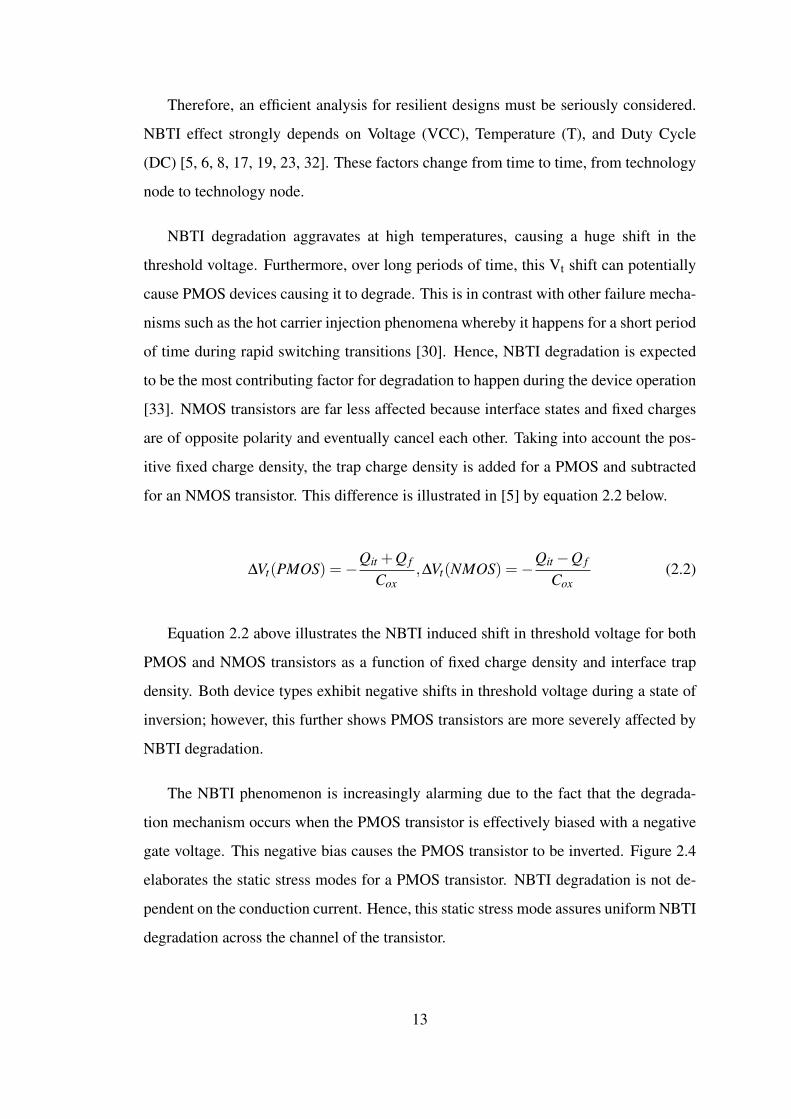
gate voltage. This negative bias causes the PMOS transistor to be inverted. Figure 2.4
elaborates the static stress modes for a PMOS transistor. NBTI degradation is not de-
pendent on the conduction current. Hence, this static stress mode assures uniform NBTI
degradation across the channel of the transistor.
13

PMOS On-State PMOS Off-State
VVD 0
VVNWELL 0DDG VV
VVS 0
DDD VV
VVG 0 VVNWELL 0
VVS 0
Figure 2.4: PMOS Stress Modes
The threshold voltage shift caused by NBTI is primarily dependent on several pa-
rameters namely temperature, voltage and stress time [19, 34–37]. The temperature is
generally within the range of 100-250C, followed by the oxide electric fields whose
value generally below 6 MV/cm [17]. Any NBTI parameters described above which
may perform below the expected value will result to the event of hot carrier degradation
instead. These parameters are comparable to those seen during the burn-in test of a de-
vice. As a matter of fact, these values are also encountered by many high-performance
ICs during normal operations.
In order to boost the circuit performance especially on SOC, designers must scale
transistor oxide, width, length and thickness together [38]. This is to ensure that the
channel resistance performance is retained from one technology node to the next gener-
ation. With the aggressive reduction of oxide thickness, less voltage must be applied to
the gate in order to sustain reliability. This threat leads to the need to lower the threshold
voltage value. During the NBTI stress, the hole concentration is higher near the gate
edge and gate-source/drain overlap region than in the channel region [39]. The NBTI
degradation near the gate edge is caused by reactions between holes and oxide defects
through a combination of routine use conditions (electric field, current, and tempera-
ture). This results in unsaturated dangling electron bonds, also referred to as interface
traps [18]. NBTI causes an analog circuit to fail due to the fact that analog operations
require higher accuracy of matched device pairs. Even small mismatches induced by
NBTI may result in circuit failure [17].
14
2.2.2 Other CMOS Defect Models
In addition to the progressive parametric degradation caused by NBTI, which is de-
scribed as the primary reliability mechanism, the circuit designers must also address
the integrity of the transistor dielectric itself. In the course of a circuit operation, this
can cause the circuit to fail. This phenomenon is typically referred to as Time De-
pendent Dielectric Breakdown (TDDB). The third critical reliability mechanism occurs
during the device switching in CMOS which is commonly referred to as Hot Carrier
Injection (HCI).
2.2.2.1 Time Dependant Dielectric Breakdown (TDDB)
Time Dependant Dielectric Breakdown (TDDB) is a wear-out phenomenon of silicon
dioxide, SiO2 the thin insulating layer between the control gate and the conducting
channel of the transistor. SiO2 has a bulk resistivity of approximately 1015 Ω - cm and a
dielectric breakdown strength of approximately 107 V/cm. This makes it the key factor
of the success in the CMOS technology due to its process advantage and high quality.
Technology scaling has driven the thickness of SiO2), tox down to the fundamental lim-
iting point of 1.2 nm. The oxide thickness of thinner than 1 nm is no longer insulated
while oxide thickness of below 1 nm may never find extensive use in CMOS technol-
ogy. This is because of excessively high oxide currents caused by TDDB [40]. Gate
dielectric is the critical part of a MOS device. Gate oxide failure usually results from
TDDB. This dielectric failure happens when there is a formation of conductive path in
the dielectric, which causes shorting of the anode and the cathode [7]. Both PMOS and
NMOS may suffer from TDDB event if both transistors are continuously stressed and
biased by the gate. As a result it will lose the control of channel current flow between
the drain and the source with a gate electronic field.
15

2.2.2.2 Hot Carrier Injection (HCI)
When a MOS transistor is in saturation, the electric field across the pinch-off region
may be high enough that carriers gain enough energy to excite electron-hole pairs. The
electron-hole pairs become components of the drain and substrate currents. The holes
(electrons) usually flow towards the p-substrate (N-well) in an N-channel (P-channel)
device, increasing the substrate currents. This scenario will have higher chances of
producing latch-up event. The excited electrons (holes) that reach the drain cause an
increase in IDSAT. In other words, it will cause a weak avalanche event. However, the
reliability concern is that part of the hot electron can penetrate the gate oxide.
The P-channel transistors are usually less susceptible to the hot electron degradation
due to the holes lower mobility, and higher effective mass. Electrons that penetrated the
gate oxide remain trapped there (in normal operating conditions). The hot electron
effect is accumulative. The negative trapped charge in the oxide, which is near the drain
of an NMOS transistor causes an increase in Vt there. The hot electron effect result is a
degradation in the NMOS IDSAT due to the higher effective Vt. It means the circuits slow
down due to the fact that the hot electron degradation has a negative feedback behavior.
Hot electron degradation is a long term reliability concern. The device life time that
the industry guarantees is 100Khr of constant operation at the worst case conditions.
However, this extreme condition is still within the industrial specification. That means
when a device frequency is tested after fabrication, the hot electron degradation with
time must be taken into account.
2.3 Burn-In Stress Test
2.3.1 Introduction
In the competitive environment of semiconductor manufacturing, accurate power dis-
sipation and reliability prediction result in significant time-to-market and profitability
improvement. Prediction quality depends on the manufacturers ability to characterize
16

process-related instabilities and defects in a given design. When the failure rate of
CMOS VLSI circuits is too high to be acceptable, a passive improvement of the relia-
bility statistical properties of the existing population can be achieved by burning-in the
product prior to shipment.
Burn-in is a process of subjecting a device to elevated temperatures and voltages
to promote early life failures of components or boards/systems in an effort to assure
that outgoing Defect Per Million (DPM) targets are met. Burn-in is an obligatory part
of microprocessor manufacturing and assures that reliability goals are achieved. It is a
critical step in the microprocessor reliability provision during High Volume Manufac-
turing (HVM). Every new product requires burn-in hardware configuration and capacity
planning before the product data are made available.
Burn-in stress test is an event when the device is exercised at elevated voltage and
temperature from the start, which is typically at time zero. The main purpose is to screen
assembly defects or to screen infant mortality defects going through a set of functional
tests. Burn-in gives a clearer picture of unit’s defects types hence determining the source
of defects. The duration of burn-in stress will help filtering out defects with other early
failure issues.
Burn-in is a process of subjecting a device to elevated temperature and voltage.
The primary goal of burn-in is to accelerate particle defects and processing problems
to failure. In other words, it weeds out Infant Mortality (IM) in the reliability bathtub
curve. Figure 2.5 shows that at 30 days, burn-in stress will screen out infant mortality
failures to guarantee product reliability in the first 30 days. Then the flat line is a
constant failure rate, known as random failures. The right most of the bathtub curve is
where failure rate begins to increase after 7 years of lifetime due to wearout.
Burn-in time (T), voltage (V) and temperature (T) conditions are process dependent.
The health and stability of the fabrication process are also key factors. In the product
qualification flow and initial production flow, units are tested at Raw Class location
before burn-in stress. Raw Class is the first location of test. The purpose of running this
test is to screen out potential assembly defects. Testing the units at raw class ensures
17

Ins
tan
tan
eo
us
Fa
ilu
re R
ate
Time
Ins
tan
tan
eo
us
Fa
ilu
re R
ate
Burn InWearout
After 7 years, fail
rate begins to
increase due to
wearout
Screen out IM failures
to ensure acceptable
DPM to customer in
first 30 days
30 days
Customer Use Time
Figure 2.5: Bathtub curve
that post burn-in socket failures can be attributed strictly to burn-in induced failure
mechanisms. Screening out defects prior to burn-in allows for what is referred to as
clean burn-in.
In the production ramp flow as illustrated in Figure 2.6, units are burned in directly
after assembly. This process is referred to as direct burn-in. Most of the semiconduc-
tor products undergo some amount of burn-in in all manufacturing flows before being
shipped to customers.
The rationale behind burn-in is to apply elevated temperature and voltage stress in
order to screen out parts with defects which would otherwise manifest as infant mortal-
ity.
18

Raw Class Testing - Screen out assembly defects
Burn-In Stress - Screen out infant mortality defects
Post Burn-In Checkout - Screen out all defects
Figure 2.6: Typical manufacturing production flow
2.3.2 Analog versus Digital Burn-In
In digital circuits,the distribution of voltage across gate and source, Vgs stress is per-
formed by dynamically toggling all transistor nodes between 0 and 1. Monitoring signal
propagation through functional blocks has been used as an empirical indicator of both
liveness, as well as the necessary toggle coverage. One of the main requirements of
burn-in set by the industrial standard is to obtain at least an 80% toggle coverage. In
other words, at least 80% of the transistors of the device will, at some point during the
test, be placed into both on and off states. However, it does not guarantee that tog-
gle coverage goals are being met, and therefore by extension, does not guarantee the
distribution of Vgs stress.
Due to the signal propagation being associated with toggle coverage, and by exten-
sion to voltage stress in digital circuits, burn-in strategies for analog circuits presently
in use across the industry are expected to be similar to digital burn-in strategies. It is for
this reason that significant effort has been extended in trying to overcome the challenges
of achieving analog signal propagation during burn-in. However, signal propagation is
not necessarily an indicator of toggle coverage. Moreover, toggle coverage often has
no meaning in analog circuits because the signal voltage levels do not swing between
logic levels in normal operation. Therefore, the actual voltage stress in analog circuit
must be carefully studied and understood. This is with the assumption that all on-chip
19

voltage regulators have been bypassed, or reprogrammed, so that external increases in
power supply voltage are directly applied to target circuit power rails.
2.3.3 Wafer Level Burn-In stress (WLBI)
The Wafer Level Burn-In (WLBI) is used to improve package-level burn-in yield and to
avoid unnecessary packaging of bad chips. Furthermore, some of the failing parts may
be repairable. With WLBI, the chips are contacted directly on the wafer. In contrast
to burn-in after packaging, WLBI does not require individual burn-in boards or spe-
cial component sockets for the various package types. That enables considerable cost
savings, especially when many different types of packages are manufactured.
However, because WLBI is generally performed on the production tester, the du-
ration of burn-in needs to be very short. Also, the temperature is restricted to be well
below package-level burn-in. Therefore, the voltage is usually increased above the
package-level burn-in voltage and special measures are taken to obtain better efficiency
in terms of duty cycle factor than in package-level burn-in.
2.3.4 High Temperature Operation Life (HTOL)
The purpose of High Temperature Operation Life (HTOL) test is to determine the effects
of burn-in bias at elevated temperature stress conditions on solid-state devices over time.
It stresses all the burn-in patterns at the maximum VCC instead of the burn-in voltage
at much higher burn-in junction temperature, typically at 125C. The setting is quiet
similar to the extended life test but with an aggressive temperature acceleration. It is
primarily being run for device reliability evaluation.
20

2.4 Summary
Reliability simulation and modeling concept have been discussed. NBTI phenomena
and its sensitivity in comparison to other reliability failure mechanisms such as HCI
and TDDB are presented and discussed. It is noted that NBTI event has been a major
threat to the SOC design especially the analog circuit design.
NBTI causes analog circuits to fail because analog operations require higher accu-
racy of matched device pairs. Even small mismatches induced by NBTI may result in
a circuit failure. In SOC design, where most of the circuit blocks (digital and analog)
are fabricated on the same chip for SOC applications, it is very critical to design right
at the first time.
Burn-in as one of the key reliability stress tests has been proven to be the key com-
ponent in ensuring the reliability robustness of a product. Some other reliability stress
tests are also being discussed. The study has found that all of these tests are having
similarities in terms of verifying the reliability concerns.
In the next chapter, the band gap reference circuit, which requires extreme accuracy,
and its applications are presented.
21


CHAPTER 3
BANDGAP REFERENCE AND ITS APPLICATIONS
The circuit performance is a function of environment where the circuit is being used.
Therefore, it is critical to minimize the effect of the environment. The environment in
this context is particularly the Process, the Voltage Supply and the Temperature (PVT).
Bandgap reference circuit has been widely used to stabilize any circuit variables es-
pecially analog circuits applications. In this chapter, this special reference circuit is
studied in detail. In order to minimize the cost for the overall work, a voltage refer-
ence circuit is desired to be designed and drawn with minimal area while minimizing
the burn-in board cost associated with external chip power delivery or filtering com-
ponents. Therefore, eliminating the need for on-die voltage regulation and eliminating
calibration or trimming to achieve an absolute accuracy performance that is tighter than
the external board voltage regulator is of interest. This aspect is important for over-
all area optimization of the chip IO ring since several IO circuits may be implemented
with a bandgap reference voltage. Due to this fact, some key applications utilizing the
bandgap reference in SOC design are described in Section 3.2. The bandgap reference
sources of error are explained in Section 3.3.
3.1 Bandgap Reference Circuit
Highly accurate voltage reference circuits are required for a variety of precision analog
circuit applications including data converters, voltage regulators, thermal sensors, bias-
ing for Phase Locked Loop (PLL), and I/O interfaces such as Universal Serial Bus 2.0

(USB2TM), Low Voltage Differential Swing (LVDS) and High-Definition Multimedia
Interface (HDMI) transmitters. The use of a voltage reference circuit for these circuit
applications generally require a fully integrated voltage reference with a continuous-
time output that exhibits a tight voltage spread and low thermal drift in production [41].
Figure 3.1 shows the basic circuit diagram of the CMOS bandgap circuit. The
bandgap voltage output, VBG, indicated in [42] with op-amp offset is given by the equa-
tion (3.1):
VBG =VBE3 +[R4R3
][KTq
lnA1A2−VOS] (3.1)
The voltage, VBE3, is the diode voltage, T is temperature, K is Boltzmanns constant,
q is the electron charge, VOS is the input referred amplifier offset, and A1/A2 is the
ratio of the two diode voltages. Resistor R4 has been designed to be equal to R5. The
bandgap voltage output, VBG, given by Equation 3.1 shows that the bandgap voltage
output is strongly dependent on the op-amp offset. Since the op-amp offset term is
effectively multiplied by a constant that depends on the ratio of resistances R4 and R3,
the offset of the op-amp is typically the main contributor to the bandgap absolute output
voltage varying from part-to-part due to random mismatch. A similar equation applies
to the low-voltage bandgap circuit architecture [1, 43].
In order to minimize cost especially for a low power product, a bandgap voltage
circuit is desired to be designed and drawn with minimal area while minimizing board
cost associated with external chip power delivery or filtering components. The filtering
components are created by adding an external capacitor to the output to create a low-
pass filter. This circuit’s output noise can be further reduced by adding another capacitor
as a passive low-pass filter. Therefore, eliminating the need for on-die voltage regulation
and eliminating calibration or trimming to achieve an absolute accuracy performance
that is tighter than the external board voltage regulator is of interest. This aspect is
important for overall area optimization of the chip I/O ring since several I/O circuits may
be implemented with a bandgap reference voltage. In addition, the voltage reference
24

R3
Vos(Startup ckt not
shown)R5
R1 R2
R4
OSV
M1M2
M3
R3
Vos(Startup ckt not
shown)R5
R1 R2
R4
OSV
M1M2
M3
R3
Vos(Startup ckt not
shown)R5
R1 R2
R4
opamp
R3
Vos(Startup ckt not
shown)R5
R1 R2
R4
To Analog Circuit
Applications
OSV
M1M2
M3
BIASV
BEV
BANDV
BGV
1I 2I 3I
1X
4I5I
1X 1X
VBE VBE VBE VBE
M=108 M=108M=4
BE3VBE2VVBE1
REFV
A1 A2
Figure 3.1: Basic CMOS Bandgap Reference Circuit.
circuit may also be required to start-up and be operational while circuits such as a PLL
may be acquiring lock or I/O circuits to reach their state of operation. Therefore, it is
desirable that the integrated voltage reference circuit is a self-contained, asynchronous
and self-starting circuit that does not depend on schemes where the voltage reference
must first be adjusted or calibrated prior to the I/O becoming functional.
3.2 Key applications utilizing Bandgap reference in SOC Design
Many system-on-chip (SOC) applications such as Universal Serial Bus 2.0 (USB2TM),
Low Voltage Differential Swing (LVDS) and High-Definition Multimedia Interface
(HDMI) transmitters require precision analog circuit applications like the Digital Ana-
log Converter (DAC), the Analog Digital Converter (ADC), the Phase-Locked Loop
(PLL) and the on-die thermal sensor. In order for these applications to operate at the
highest degree of voltage accuracy, they require the use of a bandgap reference circuit.
25

3.2.1 DAC Circuit
Many applications especially SOC, comprise of the Digital-Analog-Converter (DAC) as
well as the Analog-Digital-Converter (ADC). These converters are used for communi-
cation with the external world [44]. The typical 8-bit DAC, used to produce the signals
required to drive the RGB guns of a computer monitor, are usually current source based
circuits. The currents produced are usually converted to voltage through a simple resis-
tive termination found at each end of the cable that connects the monitor to the DAC
inside the computer. The digital to analog transformation produced by the DAC is gen-
erally covered by a set of specifications described in terms of voltage.
Since the introduction of the IBM PC in 1980, the changes and advances in raster
based display systems have been rapid and continual. Those aspects of the basic raster
display system related to the DAC specifications are introduced and are still being used
in the high speed applications.
The typical DAC used in video display is designed to be linear to the Least Sig-
nificant Bit (LSB). There are several major issues in testing the DAC to this level of
resolution. Many of the traditional DAC specifications are not typically used in the
TV/Video/Cathode Ray Tube (CRT) DAC marketplace. For instance, there are usually
no harmonic distortion or signal-to- noise ratio type specifications stated, as these are
generally reserved for high performance audio DAC [45].
The architecture and technology options as illustrated in Figure 3.2 have shown that
CMOS current-steering DAC architectures are the top choice for high speed perfor-
mance and SOC applications due to their lower cost and lower power consumption in
the SOC integration with the digital circuits. Furthermore, they are more linear than the
famous resistor-string DAC’s and they are intrinsically faster converter. [29, 46–48].
26

Figure 3.2: Architecture and techology comparisons of various DAC selections.
3.2.1.1 Output Voltage Compliance
This parameter is generally stated as a Compliance-Voltage Range (-0.5V to 1.5V)
which represents the maximum range of the output terminal voltage over which a cur-
rent source DAC will maintain its specified current-output characteristics. This then
reflects the basic ability of the current sources within the device to maintain their cur-
rents within a stated range, regardless of their summed output terminal voltage, and any
supply voltage variations.
3.2.1.2 Output Current
This parameter is also stated as a compliance type. It describes the typical full scale
current at 700 mV with the standard 75 ohm doubly terminated load (37.5 ohms total)
used on Video Electronics Standards Association (VESA) compliant video DAC [45].
The doubly terminated load implementation is to ensure maximum stability and perfor-
mance, it is important to use both a source termination resistor and an end termination
resistor. The typical voltage value would equate to having all the current sources ON
and driving a maximum current of 18.67 mA through 37.5 ohms. The min / max val-
ues would be those expected as a result of any variation of actual device performance or
27

supply voltage. The design of the DAC usually incorporates an array of constant current
sources whose sum total is used to produce the varying analog signal.
The current range of the individual current sources used in the design is not usually
stated for specification purposes but is essential if special test mode techniques are
employed that would make it possible to turn ON each current source individually. This
individual current source test mode can be extremely valuable for design validation and
manufacturing testing. It could be used as a means of measuring each current output
and checking to see it falls within the range that supports the stated Full Scale Range.
One difficulty with this measurement originates from the fact that the DAC outputs
are usually doubly terminated to ground with 75 ohm resistors and this converts the
current into voltage and unless the termination can be disconnected from ground, the
current being produced by each current source is not easily measurable by instrumenta-
tion.
3.2.1.3 DAC Resolution and Accuracy
Generally, the most important performance specifications of a DAC concern resolution
and accuracy [8]. Resolution refers to the number of unique voltage or even current
levels that the DAC is capable of producing. For typical 8-bit current source based
DAC, they ideally would produce 256 unique current values for each digital code pos-
sible. Inherent in the specification of resolution, is the property of monotonicity. The
output of a monotonic converter always changes in the same direction for an increase
in the applied digital code. The quantitative measure of monotonicity is referred to as
Differential Non Linearity (DNL) in terms of the step size.
Generally, the static absolute accuracy of a DAC can be described in terms of three
fundamental kinds of errors: offset errors, gain errors, and linearity errors. Of these,
linearity error is the most important, as usually in most cases, offset and gain errors can
be adjusted or compensated for, in the end-use application. Linearity errors are more
28

difficult and expensive to deal with in terms of added compensation at the final PC video
sub-system level. Offset and Gain errors are typically referred to as end-point errors.
3.2.1.4 Full Scale Error
Full Scale Error refers to any error found in the voltage or the current produced by the
DAC with all bits activated as ”1”. This then equates to twice the value of the DACs
Most Significant Bit (MSB) value. In a 4 Bit DAC it would be 2 times whatever the code
1000 (MSB-LSB) is ideally designed to produce. For a simple binary encoding, a linear
correspondence exists between the input codes and the output levels. The equation
referred in [45] for an N-bit DAC can be described in equation (3.2):
VO =VFS ∗N
∑i=1
bi/2i (3.2)
Note this equation reflects the fact that VFSR is different from V11 by 1 LSB.
• bi = logic levels of the binary input bits (Example: 0010 = 2) .
• N = number of input bits (Example: 4 input DAC, N = 4) .
• VFSR = Voltage Out Full Scale Reference = VFS+ - VFS−
• V11 = Voltage Out all bits On (all 1s code).
• VO = Voltage Out all bits Off (all 0s code).
Figure 3.3 is an example of the offset error alone. The actual transfer function
differs from the ideal by +2 LSBs for each code. If present, such an offset error could
be detected at each code. But, it is often only measured at the all 0s code because of
the possibility that some amount of gain error, as depicted in Figure 3.4, could also be
present [45].
Figure 3.4 reflects what can happen if only positive or negative gain error is present.
Gain error is usually expressed as a percentage, as it can affect each code by the same
percentage amount. Hence gain error by itself is undetectable at the all 0s code, but
29

Codes
Volts FS
13/16
14/16
12/16
11/16
10/16
09/16
08/16
07/16
06/16
05/16
04/16
03/16
01/16
0
0
0
0
1
0
0
0
0
1
0
0
1
1
0
0
0
0
1
0
1
0
1
0
0
1
1
0
1
1
1
0
0
0
0
1
1
0
0
1
0
1
0
1
1
1
0
1
0
0
1
1
1
0
1
1
0
1
1
1
1
1
1
1
15/16
02/16
Offset of +2 LSB across all bits
Ideal Line across all bits
Figure 3.3: 4-Bit DAC Offset error transfer function.
is detectable at the all 1s code or (Full-Scale -1 LSB) level. Figure 3.4 reflects a +/- 5
percent gain error.
Gain error is determined by first determining the offset error, then by measuring the
all 1s output voltage level (which is 1 LSB < VFSR) the full-scale reference voltage as
indicated in [45] using equation (3.3).
ErrorPercent = [(V11−Vos)/VFSR(1−2−n)]−1 (3.3)
• VFSR = Voltage Out Full Scale Reference
• V11 = Voltage Out all bits on (all 1s code).
• Vos = Voltage Measured Offset
The resolution and accuracy of the DAC are very critical to the applications. The
Absolute Accuracy Error of a DAC is the difference between the actual analog output
and the ideal output expected with a given applied digital code. This error is usually
30

Volts FS
13/16
14/16
12/16
11/16
10/16
09/16
08/16
07/16
06/16
05/16
04/16
03/16
02/16
01/16
0 0 0 0
1 0 0 0
0 1 0 0
1 1 0 0
0 0 1 0
1 0 1 0
0 1 1 0
1 1 1 0
0 0 0 1
1 0 0 1
0 1 0 1
1 1 0 1
0 0 1 1
1 0 1 1
0 1 1 1
1 1 1 1
15/16
Codes
Positive gain error
percent
Negative gain error
percent
Figure 3.4: 4-Bit DAC Gain Error transfer function.
commensurate with the DAC resolution such as less than 2 -(n+1) or 1/2 LSB of full
scale [9].
3.2.1.5 DAC Linearity (INL / DNL)
The description of Linear specifications can be broken into two major categories:
1. Integral Linearity Error or Integral Non-linearity (INL) - It is referred also to as
Relative Accuracy as covered in the gain error. It refers to the maximum de-
viation, at any point on the transfer function curve of the output level, from its
theoretical ideal value. This is ideally a straight line between zero volt and full
scale ref.
2. Differential Linearity Error (DNL) - The maximum deviation of an actual analog
output step, between adjacent input codes, from the ideal step value of + 1 LSB
(or +VFSR/2n). If the DNL error is more negative than -1 LSB, the DACs transfer
function is non-monotonic. As for the DNL, if the error is -1 LSB, the adjacent
31

Codes
Volts
FS Ref.
13/16
14/16
12/16
11/16
10/16
09/16
08/16
07/16
06/16
05/16
04/16
03/16
02/16
01/16
0 0 0 0
1 0 0 0
0 1 0 0
1 1 0 0
0 0 1 0
1 0 1 0
0 1 1 0
1 1 1 0
0 0 0 1
1 0 0 1
0 1 0 1
1 1 0 1
0 0 1 1
1 0 1 1
0 1 1 1
1 1 1 1
15/16
Integral NonLinearity > 1 / 2 LSB
Differential NonLinearity = 0
Figure 3.5: Examples of DNL and INL transfer funtion.
output step was equal to zero. A non-monotonic DAC would be one that actually
exhibits a lower output value at code N then it did for code N-1. Its transfer
function’s slope between these two points would be negative. Refer to Figure 3.5.
3.2.2 ADC circuit
The Analog-to-Digital-Converters (ADC) are important interface circuit blocks between
analog signals and digital codes which are commonly used in the electronic applica-
tions, such as data acquisition, telecommunication, precision industrial measurement,
and consumer electronics [30, 49]. As a critical part, the reliability of the ADC per-
formance strongly affects the accuracy of the overall system. Two key performance
parameters for ADCs are resolution and speed. Recently, the demand for high sam-
pling rate (more than 1 Gs/s) increases in disk operating system (DOS) and Ultra Wide
Band (UWB) system [30]. Flash ADCs are most suitable to meet the requirement of
32

high conversion rate with the simplest and fastest architecture. Moreover, by using the
deep-sub-micrometer technology, the high conversion rate can be achieved.
Similar to the DAC functional criteria, ADC also requires a higher degree of accu-
racy of voltage reference circuit. This criteria is the most critical part of analog circuit
design. To be specific, this is a key factor in defining the precision of a high resolution
ADC system. For example, a previous study done on a 14-bit ADC design has shown
that ADC requires a significant resolution in order for the thermal sensor to operate.
In the study, a temperature coefficient of 0.6 ppm/C over a range of 100C is quoted
to be a requirement for the operation provided that one LSB variation is allowed [49].
Thus, due to its precise characteristics by utilizing the bandgap reference for biasing,
the ADC has been widely used as compared to DAC design due to its better linearity
performance.
3.2.3 PLL Circuit
Clock generation using Phase Locked Loop (PLL) in today’s micro-processor products
requires a lot of effort in the design and validation phases to guarantee wide operating
range and good clock quality. Process scaling creates new challenges for analog circuits
such as the PLL, making the silicon characterization phase a very critical task.
PLL design issue is mainly related to jitter performance. Jitter is mainly caused
by the digital noise on a SOC. To be specific, jitter issue will aggravate the PLLs to
cause power supply and substrate noise issues. Figure 3.6 shows the bandgap reference
connection to the PLL. Due to being prone to the jitter issue, a voltage regulator Vref is
used to provide stable, PVT-insensitive and clean power-supply for PLL. This technique
reduces the jitter problem and minimizes the noise. The bandgap reference plays a key
role in finding not only the voltage drop across a forward biased diode but also the slope
of the current-voltage curve of a forward biased diode levels. In other words, bandgap
reference in the PLL design is used to set the voltage and to bias the current. Typically,
the voltage drop is pretty stable and it is not influenced by process drifts. As a result,
33

PLL
refV
fbV
regV
C2
C1
R1
R2
M1= PMOS
5.1V
5.1V
Figure 3.6: Bandgap reference usage on PLL design.
this factor helps in generating a stable reference voltage in a PLL design. It is noted
that as the temperature of the diode increases, the voltage drop across a forward biased
diode decreases. Therefore, it can be concluded that the voltage difference between two
diodes is directly proportional to the absolute temperature.
The bandgap reference requires the use of a higher power supply. Typically the
power supply range of the bandgap reference is between 1.2 V to 1.8 V. The Vt mis-
match in the bandgap amplifier input dominates the overall regular mismatch. The aim
is to have about 3mV offset at the amplifier which is about 20 mV variation at the out-
put. The goal is to have less than 25 mV variation which is 1 sigma variation from
the device mismatch whereas the goal for the PVT variation especially at the diodes is
about +/- 5 mV.
The bandgap reference is hard to stabilize over the wide Iload and Cload ranges.
Hence, the NMOS source-follower output stage requires more headroom so that it will
have faster response and easier to stabilize. As for the PMOS common-source output
stage, the goal is to ensure it can handle larger current loads to produce larger Vgs.
34

3.2.4 Thermal Sensor Circuit
Early generations of the thermal sensor designs were limited to off-die solutions, such
as heat-sinks or fans. But as microprocessor’s power density increased, the off-die
schemes were no longer successful in maintaining the die temperature large scale to
high volume digital CMOS processes [42]. Today’s microprocessors are starting to
implement the on-die thermal sensor. The on-die thermal sensor will help reducing the
power consumption of the overall temperature system at a minimum [50, 51]. Since,
thermal sensor errors are customer noticeable, the high degree of linearity is needed
for the thermal sensor to work in a real digital application. There are two key features
that act as indicators. The too hot scenario will cause high fan noise, low battery life,
premature throttling and in worst case, system shutdown. On the other hand, the too
cold event will produce reliability concern and hence will cause overheating [42].
To ensure to maintain the standard of the accuracy measurement, the bandgap volt-
age reference [8] is used to interface with the on-die thermal sensor circuit. The bandgap
voltage reference is used to generate a variable-slope Proportional-To-Absolute-Temperature
(PTAT) voltage (Vref) from a ∆Vbe loop to compare with the temperature dependent
diode voltage (Vbe ) for temperature comparison. One voltage is a reference to the
throttling temperature and, another set is referred to the catastrophic temperature.
The diode voltage (Vbe ) will produce a negative temperature coefficient. When the
two voltages reach the same value or level, the comparator shuts-off. This will cause
the programmed temperature to be reached at the desired level. The PTAT slope as a
function of temperature, is adjusted by looking into the DAC which controls the current
gain. Since the PTAT voltage is not skewed but reversed, an intrinsic non-linearity is
revealed. This event happens because any PTAT voltage is centered at 0K, as described
in [43] in equation (3.4) to equation (3.6) for bandgap voltage reference.
Vbg =Vbe +A∗VT (3.4)
35
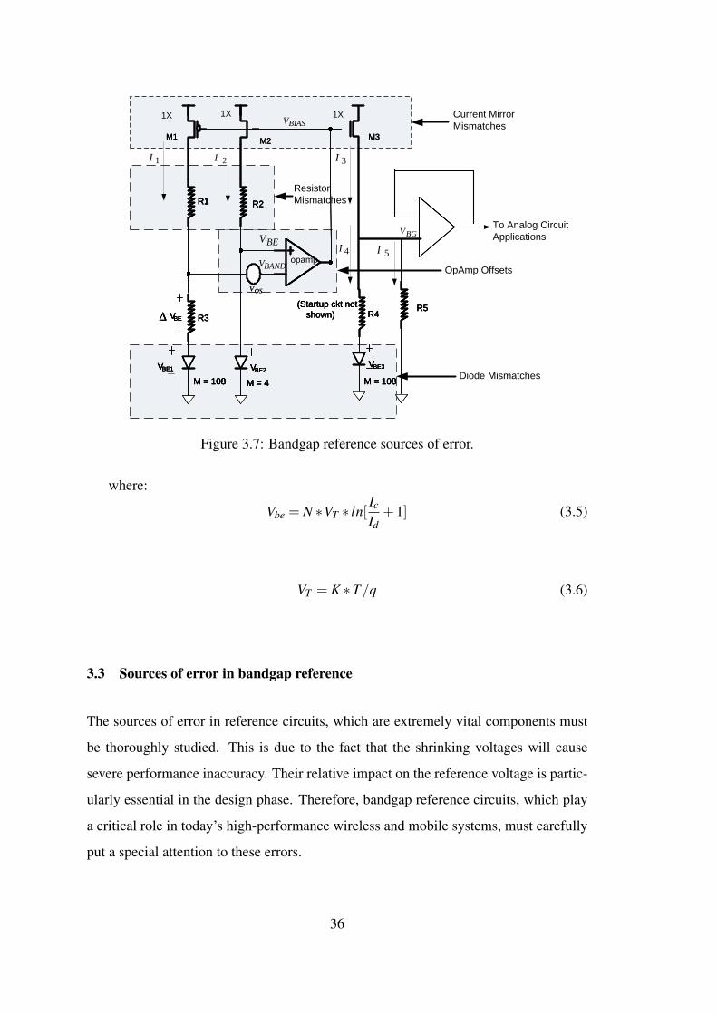
R3
M = 108
VBE2VBE1
M = 4
(Startup ckt not
shown)R5
R1 R2
R4
M = 108
VBE3
OSV
M1M2
M3
R3
M = 108
VBE2VBE1
M = 4
(Startup ckt not
shown)R5
R1 R2
R4
M = 108
VBE3
OSV
M1M2
M3
R3
M = 108
VBE2VBE1
M = 4
(Startup ckt not
shown)R5
R1 R2
R4
M = 108
VBE3
opamp
R3
M = 108
VBE2VBE1
M = 4
(Startup ckt not
shown)R5
R1 R2
R4
M = 108
VBE3
To Analog Circuit
Applications
M1M2
M3
BIASV
BEV
BANDV
BGV
1I 2I 3I
1X
4I5I
1X 1X
VBE VBE VBE VBE
Current Mirror
Mismatches
Resistor
Mismatches
OpAmp Offsets
Diode Mismatches
Figure 3.7: Bandgap reference sources of error.
where:
Vbe = N ∗VT ∗ ln[Ic
Id+1] (3.5)
VT = K ∗T/q (3.6)
3.3 Sources of error in bandgap reference
The sources of error in reference circuits, which are extremely vital components must
be thoroughly studied. This is due to the fact that the shrinking voltages will cause
severe performance inaccuracy. Their relative impact on the reference voltage is partic-
ularly essential in the design phase. Therefore, bandgap reference circuits, which play
a critical role in today’s high-performance wireless and mobile systems, must carefully
put a special attention to these errors.
36

The basic topology of the circuit used for the analysis of error sources in bandgap
references is shown in Figure 3.7. The figure shows the building blocks for the typical
bandgap reference circuits. The expressions for each sources of error in the reference
voltage of this circuit are described in sections 3.3.1 through 3.3.5
3.3.1 Mismatch in current mirror
Mismatch in the current mirror occurs from the variations of the ratio of the current
mirror. This variation may happen from various factors such as threshold voltage (Vt)
mismatch, width over length (W/L) mismatch, lambda effects of the MOS devices,
diode mismatch and resistor mismatch [52].
3.3.2 Mismatch in resistor
In this context, resistor mismatch refers to the polysilicon resistors. This type of resistor
uses a silicide block to exhibit high linearity especially to have a high degree of accuracy
which is typically around 1%. It has low capacitance to the substrate and has relatively
small mismatches. Some studies have proven that the linearity of this resistor in fact
much depends on their length, L and width, W [52, 53]. This criteria is necessary for
an accurate measurement and modeling for high precision applications.
3.3.3 Mismatch in resistor tolerance
A tolerance is defined as the deviation of any parameter from its nominal value. As a
matter of fact, the main contributor of a huge deviation of resistor tolerance, which can
be as high as 20%, is the process variation. This variation affects the VBE parameter by
changing the PTAT current flowing in the R1 and R2 resistors. Assume the δRA is the
fractional deviation of the resistors tolerance, then the relationship for the error in Vref
is given by the equation (3.7):
37

∆Vre f =−Vt ∗δRA (3.7)
3.3.4 Mismatch in operational amplifier
This error has been identified based on some studies as the most sensitive component to
mismatch [52]. Some studies have discovered that the phase margin during the op-amp
operation causes low yield in the production [54, 55]. In addition, some previous studies
have confirmed that op amp is the major contributor to the reliability issue [56, 57].
Efforts have been made to improve the existing op amp performance such as to resize
the devices and to increase the phase margin by certain allowable percentage, like 18%
while maintaining sufficient margin for Direct Current (DC) gain.
3.3.5 Mismatch in diodes
Diode mismatch is typically caused by the process variation related to the semiconduc-
tor fabrication process. The consequence of having a diode mismatch will significantly
impact the performance of the particular circuit and hence, will result in a reduced yield
of a particular product.
For the specific circuit diagram in Figure 3.7, the two diodes VBE1 and VBE2 are
meant to help minimizing the output voltage swing on the current mirror (M1 and M2).
The same thing happens on the other diode VBE3 whereby the purpose is to reduce the
output voltage swing on the transistor M3.
38

3.4 Summary
Bandgap reference definition and the nature of its application are discussed. Key appli-
cations utilizing bandgap reference in SOC design such as the DAC, ADC, PLL and the
on-die thermal sensor circuit are fundamentally described.
It is noted that all applications use the bandgap reference due to the need to have a
higher degree of accuracy of voltage reference circuits. The use of a voltage reference
circuit for these circuit applications generally require a fully integrated voltage refer-
ence with a continuous-time output that exhibits a tight voltage spread and low thermal
drift in production.
Various sources of error are noted related to the bandgap reference. Current-mirror
mismatch, which causes a mismatch in the collector currents of the bipolar transistors
in the core of the bandgap reference, is the dominant source of error. This mismatch is
a combination of various errors, namely, Vt mismatch, W/L mismatch, lambda effects
of MOS devices, diode mismatch and resistor mismatch.
In the next chapter, the actual reliability simulation and analysis with NBTI-induced
of the on-die thermal sensor and DAC circuits are presented.
39


CHAPTER 4
RELIABILITY SIMULATION
During the circuit performance, the transistor performance especially the key parame-
ters like the drain current, Ids, and the threshold voltage, Vt, will degrade over time. Due
to this event, it is very important to develop a reliability simulation. This simulation will
estimate this degradation based on the transient simulation of a circuit also known as
stress simulation. It will also evaluate the impact of this degradation on circuit perfor-
mance also known as playback simulation. In this chapter, the choice of the reliability
simulator and its key methodology is described. Two case studies,namely the On-die
Thermal Sensor and the DAC are described in terms of their voltage and temperature
sensitivities in Section 4.4 and Section 4.5 respectively.
4.1 Introduction
With the continued downscaling of feature sizes in digital integrated circuits, the vari-
ation of device parameters has become a major concern. During manufacturing, varia-
tions of process parameters are inevitable. Hence, performance parameters like power
consumption or operating frequency differ from the values they were designed for. Af-
ter manufacturing the circuit performance degrades over time due to several aging ef-
fects that cause a drift of device parameters. These effects must be considered during
a timing analysis of an aged circuit. Hot Carrier Injection (HCI) and Negative Bias
Temperature (NBTI), previously discussed in the chapter 2, are considered to be the
most critical aging effects in current technologies due to process drift. NBTI degrades

PMOS transistor characteristics and its impact can be best modeled by an increase in
the magnitude of the threshold voltages. HCI degrades the drain current of both, PMOS
and NMOS, transistor types. The traditional approach in a digital design flow to handle
reliability concerns, brought up by uncertainties of device parameters, is to introduce
safety margins. Those safety margins tend to increase in newer technologies because
the relative parameter variations caused by process variations are increasing. Further-
more, an increased impact of aging effects on circuit performance can be observed.
This increased impact of aging effects can be explained by the following two reasons;
First, the degradation is dependent on the strength of the electric fields occurring in a
device. For several technology generations, the feature sizes have been scaled more ag-
gressively than the supply voltage, resulting in an increased drift due to higher electric
fields. Second, the sensitivity of a logic gate delay according to a drift of threshold volt-
age increases with lower supply voltage. Hence, newer technologies are more sensitive
to a threshold voltage drift.
Reliability device simulator has become a critical component of the design process.
The reliability simulation has successfully demonstrated the model in most of the sig-
nificant physical failure mechanisms such as TDDB, NBTI, EM and HCI. These failure
mechanisms are modeled throughout the circuit design process to ensure that at least
the system can operate for a minimum expected useful life [2].
4.2 Choice of Reliability Simulator
A reliability simulator is a tool or software package used for verification of the re-
liability modeling, which behaves or operates as if the model is a functional system
when provided with a set of input stimulus. Several reliability simulators have been
developed due to the criticality of ensuring an accurate modeling of major degrada-
tion mechanisms such as negative bias temperature instability, hot-carrier injection, and
electro-migration. To choose a suitable simulator for this project, a few popular choices
are considered, such as Berkeley Reliability Tools (BERT), AgingSim, RelXpert and
Foundry DC Calculator.
42

Table 4.1: Comparison of various reliability simulators [1, 2].
Available Tools Attributes Applicability Disadvantage Comments
AgingSim Quasi-static calculations Intel Process Only
Not applicable for foundry
process Intel Tool
RelXpert Quasi-static calculations All Processes
Expensive, requires significant
effort and time for deployment Outsource Tool
BERT Quasi-static calculations All Processes Excessive computational work Outsource Tool
Foundry DC
Calculator DC Calculations only Foundry Process Inaccurate for AC estimations Outsource Tool
While all the reliability simulators are very powerful and popular, licensing, the ease
for debug and the compatibility with other validation languages become the decisive
factors.
After some investigation and research, it is understood that most of the simulation
tools are not able to support the work. BERT tool, which is an industry simulator, is
not able to support the work due to excessive computational and experimental work.
The RelXpert tool, which is widely known in the industry, is expensive and requires
significant effort and time for deployment. Lastly, the Foundry DC Calculator is only
applicable for the Taiwan Semiconductor Manufacturing Company (TSMC) process
and it is understood that the tool produces inaccurate simulations for AC estimations.
Table 4.1 summarizes the comparison among various simulators. Looking at the
advantages of AgingSim, it becomes clearer for the AgingSim to be adopted for this
work.
AgingSim is used to predict changes in device and circuit performance over a prod-
uct’s lifetime. It further allows the simulation of post-degraded circuits to ensure that
circuit designs meet reliability requirements at end-of-life [6, 58]. The framework of ag-
ing circuit design methodology discussed in this chapter is shown in Figure 4.1. The Ag-
ingSim will be run to cover the variations in Process, Voltage and Temperature (PVT).
Analog circuit designers should already have the skills to design the circuit that
meets the design specification at the beginning of the design stage. Now circuit design-
ers need to move one step further to include device aging impact into consideration, so
that the circuit can still meet the specification at End-Of-Life (EOL). This can only be
43

Run stress skew @
Vrel , Tjrel,
Realistic life use
conditions
Aging ReportStress file
Degpar fileCircuit netlist &
Simulation setup
Run playback skew @
Tmin- Tmax,
Vmin- Vmax,
Measurement
simulation
The Oxide Lifetime
must be > script
criteria,
and % id
degradation must
be < 20%
The playback
waveforms must be
within spec
Run
“agingsim_ scaler. pl”
to find oxide lifetime
criteria
Figure 4.1: Reliability simulation flow
achieved by running all necessary reliability simulations, and it must be a standard part
of any special circuit design procedures and be thoroughly reviewed [6].
Usually, for quality and reliability requirements such as hot electron, self-heat,
electro-migration, latch-up, etc, these failure mechanisms can checked and fixed af-
ter the designs or even after circuit layouts are done. However, special attention needs
to be paid for issues such as NBTI degradation, in particular the special circuits. Any
thermal sensor issues require changes in circuit schemes, and the late identification of
possible issues will cause negative consequences. Designers need to consciously pay
attention to the transistor NBTI degradation during the design phase to make conscious
choices to minimize the circuit sensitivity to NBTI.
For analog circuits, which is sensitive to within die variances, AgingSim provides
the aging diagnosis capability. AgingSim can be used to study the impacts of aging
differentials only, or can add the aging differentials on top of various process variances
at time zero to obtain the realistic performance distribution or failure rate of the circuit
at end of life. AgingSim must be performed to obtain a realistic risk evaluation for the
reliability qualification of the circuit design. Without thorough reliability awareness,
the analog circuits are susceptible to mismatches and thus impact the overall circuit
performance [6].
44

The effectiveness of the reliability simulator specifically for this project has been
proven and verified across major process technologies since the early 250nm until the
recent sub-micron process technology such as the 14nm technology. Major mainstream
CPU have used this reliability simulator effectively particularly for speed path analy-
sis. During the early development of the simulation tool, it was hard to correlate the
results. For example, many CPU products were attempting to approximate burn-in data
to 7 year simulations. It was found that the results will correlate when the users use the
correct inputs. Across many process technologies, this reliability simulator has been ex-
periencing major improvements. Truly, this reliability tool can predict correct behavior
as compared to post-stress silicon behavior.
4.3 Methodology
The first step in the simulation methodology of this case study is to enable reliability
analysis of the analog SOC particularly the on-die thermal sensor and the DAC due to
NBTI-induced circuit aging. Large magnitudes of voltage and temperature variations
can occur even during several instants of microprocessor execution, leading the motiva-
tion to study this reliability failure mechanisms even deeper [59].
This simulation study gives an opportunity for observing voltage and temperature
variations. The methodology is event-driven, where at each workload arrival or finish,
NBTI as part of the critical reliability failure mechanisms is invoked. Depending on
the way the circuit designers define the reliability model, the simulation result can be
varied by varying the voltage and temperature knobs; this results in a significant NBTI
degradation. Hence, voltage and temperature are sampled at each workload event and
the corresponding NBTI failure rate is computed.
Reliability simulator estimates the transistor performance such as IDSAT and Vt
degradation based on the transient simulation of a circuit under stress. It evaluates the
impact of this degradation on circuit performance under playback simulation. Reliabil-
ity simulator not only models Negative Bias Temperature Instability (NBTI) but also
45

models Hot Carrier Injection (HCI) and other devices reliability modes. The simulator
uses a combination of other simulators to complete the whole AgingSim.
For a specific NBTI mechanism, the physical model of the simulator is based on
equations (4.1),(4.2),(4.3) and (4.4). This equation as explained in [1] shows the thresh-
old voltage shift of PMOS transistor with different design parameters.
T T F(s) = MT T F ∗ f (VT P,L)∗A (4.1)
A = exp(−γ∗E)∗B (4.2)
B = exp[Ea
k∗ [ 1
Tj +273− 1
398]∗C]β (4.3)
C =[
δVT P∗FC (4.4)
The parameters in (4.1),(4.2),(4.3) and (4.4) are as follow:
• E is electric field (V/Tox) across gate oxide
• T j is the junction temperature
• MTTF is mean time to failure
• TTF(s) is scaled time to failure in seconds because of voltage and temperaturescaling
• F(Vtp, L) is geometry scaling function for aging
• Ea is thermal activation energy
• FC is Vt shift defined as failure criterion for modeling.
• β is the process dependent variables.
46

The shift in Vt, the threshold voltage for a time varying waveform, as elaborated in
[1] can be calculated using the quasi-static time integral in (4.5).
T T F =1
1t ′ ∗
∫ dtT T F(t)
=1
Avg(1/T T F(t))(4.5)
In stress mode, the reliability simulator calculates the transistor Vt shift, using the
complete simulated waveform and equations (4.1), (4.2), (4.3) and (4.4). In playback
mode, the simulator re-runs spice simulations with a degraded threshold voltage to cal-
culate the shift in delay after aging.
It is noted that even though NBTI degradation occurs under elevated voltage and
temperature, the NBTI phenomena do show some levels of relaxation [4]. There are
two types of relaxation that need to be seriously considered for the circuit reliability
modeling.
1. Fast relaxation : This relaxation occurs as soon as the stress is removed. It is re-
sponsible for reduced AC degradation even after accounting for the transistor ON
time. However, this relaxation mode is not covered in this reliability simulation.
2. Extended relaxation : This relaxation occurs as the device is kept unbiased. This
reliability tool has already accounted for this relaxation mode into the simulation.
Most of the aging data have already been accounted for this relaxation since the
devices are tested much later after they have been removed from stress.
Because of the above two relaxation modes, a device under continuous usage may
suffer a higher degradation than what the reliability simulation predicts. Figure
4.2 illustrates the two relaxation modes.
47

Degradation Recovery RecoveryDegradation
Fast
Degradation
Vt/Id
shift
Figure 4.2: NBTI periodic stress and relaxation [4].
4.3.1 Assumptions of the reliability simulation model
Reliability simulation models are often used to extrapolate failure rates. Therefore,
it is very important to validate whether the models chosen are consistent with whatever
data are available. This section describes several assumptions used to ensure the model
used for this case study is acceptable.
1. Constant failure rate assumption: According to J. Bernstein et al. [60], it is crit-
ical to use an exponential distribution for a complex electronic application to
estimate the overall failure rate. Even though most of the key circuit reliability
failure mechanisms such as NBTI, TDDB and HCI do not correlate with the ex-
ponential distributions, it is justified to use this assumption due to the criticality
of such events to occur. J. Bernstein et al. [60] in their comprehensive reliability
modeling development also have demonstrated that it is not necessary to figure
out the distribution for each of the failure mechanism’s failure rate. In addition,
an article by Reliasoft has a similar argument that implies the urgency to run relia-
bility simulation under the actual usage conditions. Several mathematical models
have been developed, implemented and well explained but the benefits are far
from what have been gained in the actual usage conditions [61] . Both statements
suggest that the failure rate for each of the failure mechanisms will be averaged
out in order to produce a constant level of the failure rate based on realistic usage
conditions.
48
2. Equal contribution assumption: This assumption is subjected to the failure anal-
ysis results which leads to determining the actual distribution of field failures. J.
Bernstein et al. [60] commented that this assumption is about how the device
is designed properly as minimum reliability failure mechanism as possible. Due
to the reliability awareness, electronic components are now designed at the rea-
sonable cliff of the design specifications. When any potential failure mechanism
arises, specific design and manufacturing techniques will be developed to miti-
gate the risk of the failure. This assumption is the extension of the first assump-
tion whereby not even one failure mechanism dominates. All are equally likely
and the resulting failure distributions are similar to the constant rate processes.
3. Proportional acceleration assumption: It is shown by J. Bernstein et al. [60]
that the constant failure rate-based reliability for electronic components allows
the manufacturer to test parts under accelerated conditions on condition that all
failure mechanisms are accelerated in approximately the same proportion. Data
extrapolation can be done once the result of the failure rate is available taking into
account factors such as applied voltage, temperature, and speed of the devices.
However, the drawback is that the accelerated stress test may cause reliability
problems if this assumption is wrong. Therefore this assumption needs to be
thoroughly analyzed and done right at the first time.
4. Linear superposition assumption: System failure rate is linearly modeled as a sum
of individual failure mechanisms. This assumption is not taking the consideration
of interactions with different reliability failure mechanisms. For example, NBTI
may overlap with the HCI event, but the interrelation is too complicated and is
typically insignificant and negligible.
5. Technology dependence assumption: All model parameters for each failure mech-
anism are dependent on process technology. For different process technologies,
model parameters typically vary, but for the same process technology, they are
assumed to be constant. This assumption allows technology and circuit designers
to mitigate the risk of the proven model parameters by characterizing with typical
49

sample structures to determine the robustness of each model parameter. Fur-
thermore, both technology and circuit designers can use these extracted model
parameters to estimate the failure rate of by the same process technology.
4.3.2 Stress Mode
A ”Stress” Mode is used to calculate the amount of device degradation after arbitrary
periods of time. During this mode, the AgingSim will calculate device degradation
during a short transient simulation and extrapolate the degradation out to the desired
degradation time. This mode is run under the assumption that the signal from the short
transient simulation is repeated throughout the entire degradation time. At the end
of the stress mode, the simulation will create an age report containing the end-of-life
degradation values for each transistor.
4.3.3 Playback Mode
Unlike ”Stress” mode, the ”Playback” mode is used to simulate degraded circuit per-
formance based on Stressing Mode results.
In general, the AgingSim flow allows circuit designers to define the ”Stress” and
”Playback” corner list in the global corner definition file which can be used by all the
circuit designers who are working on the same interface design or reused for other
project. In the design flow, circuit designers can define a normal corner list together
with the ”Stress” and the ”Playback” corner list in the script to kick off the regression in
parallel. Hence, the final result table will display all the normal corners and AgingSim
corner’s run results for comparison. This table is needed in order to quickly identify
any circuit performance issues.
50
4.4 Case Study 1 : On-Die Thermal Sensor Reliability Prediction
The on-die thermal sensor has performed a simple but important task for many gen-
erations of Intel processors. Its purpose is to monitor the junction temperature on-die
and to determine whether the operating temperature has exceeded the pre-programmed
the hot processor (PROCHOT) reference temperature. This thermal management fea-
ture allows the system designer to design cooling solution based on real-life power
consumption, not peak power. Should the junction temperature (Tj) rise above the
PROCHOT trip point, the processor throttles its frequency and voltage in an effort to
maintain a Tj at or below the trip point.
To demonstrate good and consistent linearity across voltage and temperature, the on-
die thermal sensor has been selected as a vehicle in this case study. The key motivation
is to observe how severe is the NBTI mechanism affecting the on-die thermal sensor
performance.
4.4.1 On-Die Thermal Sensor Design
Temperature monitoring sensors can be categorized either as off-die or on-die whereby
they are either built-in or embedded into the silicon design.Off-chip techniques can be
further sub-classified as based either on the contact methods or the non-contact methods.
Example of the usage of contrast materials such as liquid crystals, phosphorus or the
use of Atomic Force Microscopes. In contrast, the non-contact methods include infrared
thermography, reflectometric and interferometric techniques. Since all these techniques
require a direct optical access to the silicon die, they are usually restricted to failure
analysis [62].
On-die thermal sensors have a silicon area overhead but they provide significant
flexibility for the test procedure, allowing both laboratory and in-field testing. The
built-in thermal sensor output can be proportional to the absolute temperature or could
be proportional to the difference of temperature at two points of the silicon surface.
51

VCCDDR(1.5V - 1.8V)
VCCQ
(1.12V)Voltage
regulator–
Thermal
sensorInputs
from
core
Hot
Cat
VCCDDR
VCCQ
(1.12V)Voltage
regulator–
SubBandgap
Thermal
sensorInputs
from
core
Hot
Cat
Figure 4.3: Thermal Sensor Block Diagram.
Thus, implying the need for two temperature transducers, and relative temperature mea-
surement [63].
On-die thermal sensors are preferred over off-die ones because of their fast response,
low cost and the fact that they can be designed for low area and low power overhead
[62]. However, the drawback is that they have additional design constraints such as
CMOS process technology compliance, unregulated power supply and calibration limi-
tations. Also, in an on-chip thermal sensor, the reference will be susceptible to the same
inputs as the sensor. Built-in/on-chip thermal sensors can be classified on the basis of
their output type, circuit type and process technology [42].
The block diagram of the on-die thermal sensor circuit used in this case study is
shown in Figure 4.3. The circuit consists of the thermal sensor and a voltage regulator
with a Double Data Rate (DDR) power supply (VCCDDR) of 1.5V-1.8V. The output
stage logic power voltage (VCCQ) of 1.12V supplies the thermal sensor.
The thermal sensor allows the system designer to design a cooling solution based
on the real-life power consumption, not the peak power. If the junction temperature,
Tj, rises above the hot trip point, the micro-processor throttles its frequency and voltage
52

in an effort to maintain Tj at or below the trip point. Another output from the thermal
sensor is the catastrophic shutdown (Cat). This is a feature that prevents permanent
damage to the micro-processor should hot thermal management fail allowing the micro-
processor to go into thermal runaway. It accomplishes this by disabling all clocks and
asserting a special thermal sensor signal, which will cause the system to collapse the
Vcc supply and prevent leakage from heating the processor further. The Cat event
indicator must trigger below the threshold where damage occurs to the micro-processor,
but above the hot trip point.
Bandgap voltage reference, as illustrated in Chapter 3, Figure 3.1, is a high-performance
analog circuit for applications in a host of analog, digital, and mixed-signal integrated
systems [1]. For all these applications, the accuracy of the bandgap reference voltage is
crucial as it can severely limit system functionality. This is especially very important in
the case of sensitive blocks like thermal sensors [52]. The thermal sensor is an on-die
analog circuit used by microprocessors for clock throttling, thermal catastrophic protec-
tion, and power management. Unlike thermal diodes, with no external pin limitation,
thermal sensors can be placed in multiple locations within a microprocessor to capture
the within-die temperature profile [54]. However, on-die thermal sensors usually have
poorer accuracy than the external temperature sensing chips used by thermal diodes,
which are fabricated on the trailing edge analog CMOS processes [42].
The DAC based circuits rely on the comparison of a PTAT voltage and a comple-
mentary to absolute temperature (CTAT) base-emitter voltage for temperature measure-
ment, without the need of an accurate ADC [64]. They are relatively simple to imple-
ment but are difficult to deliver with good quality over a wide temperature operating
range [51].
The circuit as illustrated in Chapter 3, Figure 3.1 generates a variable-slope PTAT
voltage (VREF) from a ∆VBE loop and compares it against the diode voltage (VBE).
The VBE has a negative temperature coefficient so when the two voltages reach the
same level, a comparator trips, indicating that the programmed temperature has been
reached [65]]. PTAT slope as a function of temperature is adjusted using current DAC
53

with variable gain M. Since the PTAT voltage is not shifted but rotated, intrinsic non-
linearity is introduced. This occurs because any PTAT voltage is pivoted at 0K, as
described in [42] in the following equation for VREF [66].
VREF(T ) = M[nKT
qlnN−Vo f f ]
RV REF
∣∣∣T−T 0
Rb
∣∣∣T−T 0
(4.6)
VSBG = [R5
R4+R5]VBE3 +[
R5R4R3(R4+R5)
][KTq
lnA1A2−VOS] (4.7)
If R5=∞, then I4=I3
VSBG =VBE3 +[R4R3
][KTq
lnA1A2−VOS] (4.8)
VSBG =VBE3 + I3I4 (4.9)
Equation (4.6) is based on the schematic of the thermal sensor circuit as illustrated
in Chapter 3, Figure 3.1. All transistors are sized and biased such that they are operating
in saturation region. Transistor M1 provides a bias for the current mirror PMOS tran-
sistors (M2 and M3). The drain current of the current mirror PMOS transistors (I2 and
I3) drives the diode connected to the op-amp, generating voltage difference of VBE and
VBAND. The output of the op-amp is connected to M3 which then connects to the ther-
mal sensor circuit. Equation 4.7 to 4.9 compares the PTAT (VREF) against the VBAND
voltage, which is obtained by placing a diode and a resistor (GB NWell) in series. The
diode voltage (VBE) has a negative temperature coefficient and the resistor has a posi-
tive temperature coefficient but not as large as that of the VBE in absolute value. Thus,
the total temperature coefficient for VBAND is still negative since VBE dominates. When
the two voltages are crossed, a comparator will trip, indicating that the programmed
temperature has been reached.
54

4.4.2 AgingSim Process Step
NBTI simulation is performed using the AgingSim tool covering electrical over-stress
analysis and statistical simulations. The AgingSim and analysis are done in Cadence
Analog Artist environment based on the circuit as illustrated in Chapter 3, Figure 3.1.
For this case study, the NBTI behavior of the thermal sensor circuit under normal and
extreme conditions was simulated. Thermal sensor AgingSim was run in a 3-Step Pro-
cess.
1. Generate a fresh (non-degraded) waveform at the typical circuit operating condi-
tion (VCC and Temperature).
2. Turn on the AgingSim Stressing Mode to calculate the amount of degradation on
each transistor. This was done at a slightly higher voltage and temperature to get
a more conservative estimate of the degradation.
3. Turn on the AgingSim Playback Mode to simulate the degraded waveform, using
the degradation calculated in the Stressing Mode. This was done at the operating
conditions used for the fresh simulation (step 1), in order to make the comparison
between fresh and degraded waveforms.
Out of these three steps, step 3) is the most general representation in which the
stressing mode simulation does not have to be at the same conditions as the fresh and
degraded simulations. If quality and reliability specifies that the Stressing Mode can be
run at the normal operating condition (same as fresh and degraded simulations), then
steps 1 and 2 can be combined into a single operation. In this case study, the fresh curve
was generated at the same time as the age report.
AgingSim playback mode analysis was done under the following conditions on
three standard corners.
1. RSSS refers to a slow corner
2. TTTT refers to a typical corner
3. RFFF refers to a fast corner
55

The simulation, which covers these three process corners, uses the pre-layout schemat-
ics with proper loading. For this analysis, the circuit was aged for 7 years life time to
check the thermal sensor circuit functionality and the effect of NBTI degradation un-
der burn-in mode conditions. Table 4.2 shows the AgingSim parameter settings at time
zero, stressing and playback modes. In order to guarantee a good coverage of reliabil-
ity analysis, a process skew is almost mandatory. The skewing of the process corners
means the difference in propagation delay times between corresponding outputs on any
two like devices when both devices operate under identical conditions. Process skew
quantifies skew due to process variation in the manufacturing process (skew caused by
lot-to-lot variation). It excludes variations in supply voltage, operating temperature,
output loading, input edge rate, input frequency, etc. Hence, process skew is an out-
put skew over several devices covering slow, typical and fast corners in all 3 different
modes. For the fresh mode, the stress voltage is at 1.8V nominal whereas for the burn-in
and age modes, the stress voltage is elevated at 2.5V. As for the temperature, the differ-
ence between the fresh and the burn-in mode is by 10C. Last but not least, the fresh
mode is obviously defined to be time zero, the burn-in mode is at 500hrs and the Age
mode is simulated to 7 years lifetime. These parameters were used for the AgingSim of
the on-die thermal sensor.
The result in Table 4.3 revealed that under burn-in condition, the thick gate oxide
in the thermal sensor circuit block has bigger lifetime prediction margin which is until
1000 years of operation. As a matter of fact, the lifetime of the thick gate oxide at time
zero and after burn-in stress remains the same. On the other hand, the thin gate oxide
has shorter lifetime prediction, which can only survive between 11.5 days for NMOS
thin gate oxide to 1.85 months for PMOS thin gate oxide. This analysis has proven
that the thick gate oxide reliability is more robust as compared to the thin gate oxide
reliability.
To further zoom into a specific thermal sensor block AgingSim analysis, the matched
devices were analyzed and a slightly different degradation behavior was observed. The
degradation of the matched devices in VREG Operational Amplifier (Op Amp) was re-
ported having slightly different degradation percentage between 0.36% and 1.73% as
56

Table 4.2: AgingSim Settings across 3 different modes.
7 years500 hrsTime 0Use time
110'C110"C100'C
1.8V2.5V1.8VStress Voltage
Stress Skew
Burn In (Stressing Mode)FreshParameters
7 years500 hrsTime 0
110'C110"C100'CTemperature
Age (Playback Mode)Burn In (Stressing Mode)FreshParameters
Slow,Typical,
Fast
Slow,Typical,
FastSlow,Typical,
Fast
Table 4.3: AgingSim - Post Stress Result.
Thin N 232 Yrs 11.5 Days
Thin P 188 Yrs 1.85 Months
Thick N 1000 Yrs 1000Yrs
Thick P 1000 Yrs 1000Yrs
Pass/Fail Pass Pass
Gate
Oxid
e
Lif
eti
me
Fresh
Condition
Burn-in
Condition Paramater
indicated in Table 4.4. These two matched devices were expected to have similar Idsat
percentage but transistor M1213 had about 1.73% degradation. After thorough inves-
tigation on the specific node, the degradation was deemed acceptable to be below the
allowable percent degradation. The goal was set to be below 10% degradation.
AgingSim covers a range of process, voltage and temperature (PVT) and therefore
it is very crucial to perform analog aging verifications across multiple PVT conditions.
Table 4.4: Matched devices in Op Amp.
Oxide Lifetime percent Id (%) Idmax (mA) Vt shift (V) Vt mismatch (mV) Node
1000y 2.29E-32 0.03073 M1220
1000y 2.15E-32 0.0303 M1221
1000y 2.047 -0.05951 -0.01179 2.329 M1210
1000y 2.047 -0.05952 -0.01179 2.329 M1211
1000y 2.047 -0.06136 -0.002071 2.329 M1215
1000y 0.3612 -0.02976 -0.009918 0.9102 M1212
1000y 1.726 -0.02946 1.99 M1213
1000y 6.07E-33 0.02945 M1225
1000y 2.05E-33 0.02939 M1226
1000y 0 0.02943 M1224
1000y 0 0.0294 M1227
1000y 0 0.04549 M1228
1000y 0 0.06141 M1229
1000y 5.35E-22 0.352 M1230
1000y 0 0.352 M1231
1000y 0 0.06031 M1232
57

In special circuits like thermal sensors, NBTI can pose a serious reliability concern as
even a small variation in bias currents can cause significant gain errors [67].
4.4.3 Voltage Sensitivity Analysis
Higher voltage difference between gate and source will result in a higher degradation.
As explained in the theory [19, 68], this is a result of the higher electric field causing
a larger number of interface traps. According to Schroder et al. oxide electric field
enhances NBTI and causes certain key process parameter to be shifted [5]. This scenario
is determined by measuring the time-to-fail (TTF).
TTF in [5, 18] is a function of the following relationship:
• When the stress voltage, Vstress, increases, the TTF decreases.
• When the difference between the nominal voltage, VCC, and Vt increases, theTTF goes down.
• Last but not least, as the temperature goes up, the TTF will be on the oppositedirection.
The worst case situation is when the unit is operated or is kept at a high voltage
most of the time, but operated at low voltage sometimes [32].
Figure 4.4 shows the thermal sensor voltage output comparison between the before-
stressed and the after-stressed simulations. Looking at the waveforms, the simulations
clearly show that any mismatch developing by the thermal sensor circuit shifts the out-
put characteristic by roughly the amount of the threshold voltage difference. The post
stressed simulation represents after 7 years, which is a typical product lifetime. Of note,
it was observed that the thermal sensor DC output characteristic shifted to right side of
the before-stress curve. The implication of the degradation is that it lower the drive
current, Id and hence, slowing down the circuit operation.
58

Thermal Sensor Output voltage before and after stress
-0.2
0
0.2
0.4
0.6
0.8
1
1.2
0 2 4 6 8 10
Time (ns)
No
de
vo
lta
ge
(V
)
Before Stress After Stress
Figure 4.4: AgingSim Voltage variations.
Figure 4.5: Lifetime as a function as temperature [5].
4.4.4 Temperature Sensitivity Analysis
Higher temperature stress significantly enhances NBTI effects. (Proportional to ∼T4)
[18]. Figure 4.5 shows the relation between NBTI lifetime and nitrogen concentration
in the gate insulator. The increase in nitrogen concentration, which suppresses boron
penetration for the scaling-down gate insulator of PMOS transistor, causes the degrada-
tion of NBTI characteristics. As indicated in [18], there are 3 key equations that show
the temperature relationships to the NBTI. Equation (4.10) shows the interface trap den-
sity is inversely proportional to the oxide thickness tox while Equation (4.11) reveals the
fixed oxide charge is independent of tox. The relationship between Equation (4.10) and
59

-10
-8
-6
-4
-2
0
2
4
-20 0 20 40 60 80 100 120 140
Tem
pe
ratu
re S
hif
t, 'C
Simulation performed @ 80'C DAC code 99
Non DAC
DAC
+/- 1’C
RelBudget
T fresh, ‘C
Figure 4.6: AgingSim considering temperature variation.
(4.11) suggest that NBTI is worse for thinner oxides. However, this is not always ob-
served because NBTI is highly dependent on the process conditions. Equation (4.12)
shows the dependence of Vt shift on inverse of the stress temperature (1/T). As a result,
NBTI degrades more severely the higher the temperature. High performance micropro-
cessors and SOCs can have hot spots in a circuit design leading to large temperature
gradients across a chip.
∆Nit ∝ exp0.2kT
(4.10)
∆N f ∝ exp−0.15
kT(4.11)
∆Vt = f (∆Nit,∆Nf) (4.12)
where:
1. Nit is the interface states
2. Nf is the fixed oxide charge
60

Figure 4.6 shows the AgingSim temperature profile of the thermal sensor circuit.
The line points and the dotted points were used to compare between the DAC circuit
and the non-DAC circuit building block that connects to the thermal sensor circuit. The
temperature difference (-30C∼130C ) resulted in an aging difference of up to ±1C
between the lowest temperatures to the highest.
It is important to know accurately what each unit is going through, from a temper-
ature perspective, at each burn-in session. This can be achieved through the thermal
sensor and a proper calibration of the thermal sensor at a unit level. Hence, it is critical
to observe that NBTI is highly sensitive to the operating temperature. The amount of
degradation observed is strongly dependent on the temperature of the chip [36].
4.5 Case Study 2 : Digital Analog Converter Reliability Prediction
The function of the DAC circuit is to drive an analog signal where the luminance of
the signal is coded as the output voltage swing [69]. It is a key circuit to the graphics
engine which is used to drive a cathode-ray tube (CRT) type analog display. The CRT
DAC is a precision analog circuit that requires thorough characterization since many of
the performance aspects of the CRT DAC are not feasible or cost-effective to be tested
during high volume manufacturing. The CRT DAC performance is critical since its
performance directly affects the display quality and since poor visual quality can lead
to eye fatigue.
To demonstrate a good and consistent performance across voltage and tempera-
ture, the CRT DAC has been selected as a second vehicle in this case study. The key
motivation is to observe the severity of the NBTI mechanism affecting the CRT DAC
performance.
61

8- bit
D/A
8- bit DAC
Bandgap &
CRT & TVO
Reference
Circuit Blocks
8- bit
D/A
8- bit
D/A
Test Logic
Bandgap
Edge of Die
8- bit
D/A
8- bit DAC
Bandgap &
CRT
Reference
Circuit Blocks
8- bit
D/A
8- bit
D/A
Test Logic
Bandgap
Edge of Die
Figure 4.7: The 8-bit CRT DAC block diagram.
4.5.1 Digital Analog Converter Design
Even though a device pair mismatch of 1 mV to 2 mV may seem to be insignificant,
certain special circuits do require absolute levels of matching. One of the examples is
a DAC circuit. A DAC requires extreme level of matching [8]. The typical 8 Bit CRT
DAC used to produce the signals required to drive the RGB guns of a CRT-based PC
monitor are usually current source based circuits. Figure 4.7 shows the high level block
diagram showing the bandgap interface with the 8-bit CRT DAC.
Memory controller chip designs that integrate a graphic engine to support enhanced
video applications have become an important feature as well as a major cost reduc-
tion aspect for the PC platform. Future chip designs will continue to integrate a graphic
engine on-die to provide original equipment manufacturers the flexibility to design cost-
effective PC platforms without the need for an external video card. It is therefore es-
sential to perform a thorough characterization of the video DAC for each chip product
that integrate the graphics engine.
The performance of the DAC is critical for achieving excellent video quality. The
required accuracy of the DAC is based on the differential gain and the phase distortion
62

specifications for TV. The architecture is designed as a current-steering architecture to
achieve high accuracy and low distortion of the analog video signal from the mother-
board ground level, i.e. zero volts, to the maximum nominal analog video signal swing
of 1.3 V. The digital input to each DAC is latched on the rising edge of each clock and
converted to an analog current. For a given digital input, the current source outputs are
either summed together and directed to the output pin or directed to the motherboard
ground plane by the differential current switches. An analog video voltage is created
from the DAC output current flowing into the termination resistors. The video level
specifications for the various video formats along with the effective load termination
determine the required output current of the DAC circuit. The Least Significant Bit
(LSB) output voltage is a function of the video format supported and normally ranges
between 684 µV to 1.27 mV above the motherboard ground.
Knowing the circuit mismatch sensitivity on this special circuits, paired devices are
typically designed using longer dimensions, i.e. the L and W values of the CMOS
transistors. The main purpose is to minimize process variation and to meet the desired
initial matching characteristics and requirements.
To meet the minimum requirement for 10-bit accuracy, the digital input word must
have an error less than 50 percent of the LSB. To calculate the sensitivity of a device
mismatch, the Integral Non-Linearity (INL) can be used as an example. The INL is
defined in [17] as the maximum deviation from the ideal DC transfer curve, and for an
N-bit DAC, it can be expressed as equation (4.13)
INL≈√
2N−1 ∗∆Id/Id ∗LSB (4.13)
4.5.2 AgingSim Process Flow
NBTI simulation for the DAC circuit is done through AgingSim covering electrical
over-stress analysis and statistical simulations. The AgingSim and analysis are done in
63

VCCA=3.3V8 LSB (CRT)
32 LSB (TV)
CRT Current
Source Array
Master Reference CRT D/A Biasing (for 3 Channels)
VSSA
Bandgap
Voltage
Reference
+
-
~ 0.762V
~ 1.21V
Rset = 1300, 0.5%
for 37.5 D/A Load
VCCA
BIAS1
BIAS2
1 : 1
I ~ 586A
I ~ 586A
CRTIREF
8LSB (CRT)
VSSA
fdbk
BIASM
Level
Shifter
(3.3V)
V1
BIASC
~0.7V
MBIAS2
1 : 1
MBIAS1
TGVDNMOS
Or TGNMOS
VCCA=3.3V8 LSB (CRT)
32 LSB (TV)
CRT Current
Source Array
Master Reference CRT D/A Biasing (for 3 Channels)
VSSA
Bandgap
Voltage
Reference
Bandgap
Voltage
Reference
+
-
~ 0.762V
~ 1.21V
Rset = 1300, 0.5%
for 37.5 D/A Load
VCCA
BIAS1
BIAS2
1 : 1
I ~ 586A
I ~ 586A
CRTIREF
8LSB (CRT)
VSSA
fdbk
BIASM
Level
Shifter
(3.3V)
V1
BIASC
~0.7V
MBIAS2
1 : 1
MBIAS1
TGVDNMOS
Or TGNMOS
Figure 4.8: Simplified circuit diagram of 8-bit CRT DAC [1].
Cadence Analog Artist environment based on the circuit in Figure 4.8. For this case
study, the NBTI behavior of the DAC circuit under normal and extreme conditions was
simulated, similar to simulation conducted on the first case study explained in Section
4.4.2.
DAC AgingSim was also run in a 3-Step Process.
1. Generate a fresh (non-degraded) waveform at the typical circuit operating condi-
tion (VCC and Temperature). In DAC case, the nominal voltage and temperature
are set at 3.3V and 100C respectively.
2. Turn on the AgingSim stressing mode to calculate the amount of degradation on
each transistor of the current source and the differential switch. This was done at
4.6V and 110C to get a more conservative estimate of the degradation.
64

Table 4.5: AgingSim parameters across three different conditions
Parameters Fresh Burn In (Stressing Mode) Age (Playback Mode)
Stress Skew Typical Typical Typical
Stress Voltage 3.3V 4.6V 3.3V
Temperature 100'C 110"C 110'C
Use time Time 0 500 hrs 7 years
3. Turn on the AgingSim playback mode to simulate the degraded waveform, using
the degradation calculated in the stressing mode. This was done at 3.3V and
100C for the fresh simulation (step 1), in order to make the comparison between
fresh and degraded waveforms.
Similar to the simulation run on the first case study, step 3 is determined to be the
most general representation in which the stressing mode simulation does not have to be
at the same conditions as the fresh and degraded simulations. If quality and reliability
specifies that the stressing mode can be run at the normal operating condition, which is
the same as fresh and degraded simulations, then steps 1 and 2 can be combined into a
single operation. In this case study, the fresh curve was generated at the same time as
the age report.
AgingSim playback mode analysis was done under the typical corner (TTTT). The
analysis was done by invoking the DAC schematics layout with proper parameters
loaded. For this analysis, the circuit was aged for 7 years life time to check the DAC
circuit functionality and the effect of NBTI degradation under burn-in mode conditions.
Table 4.5 shows a comparison among three different conditions.
4.5.3 DAC Circuit Design
Under a specific DAC block AgingSim analysis, the analysis is primarily focused
on the matched devices in Figure 4.9. After a thorough analysis is done, the matched
devices reveal a slightly different degradation behavior. Ultimately, the DAC design is
65

CRT DAC
VCCA = 3.3V
RLoad = 37.5
Vout : 0V to 0.7V
VCCA/2
Bias1 M1
M4
M2
M3
Package
Ball
VCCA
Bias2
Switch Driver
All Transistors are Thick Gate PMOS
Current Source
Differential Switch
Vout
CRT DAC
VCCA = 3.3V
RLoad = 37.5
Vout : 0V to 0.7V
VCCA/2
Bias1 M1
M4
M2
M3
Package
Ball
VCCA
Bias2
Switch Driver
VCCA = 3.3V
RLoad = 37.5RLoad = 37.5RLoad = 37.5
Vout : 0V to 0.7V
VCCA/2
Bias1 M1
M4
M2
M3
Package
Ball
VCCA
Bias2
Switch Driver
All Transistors are Thick Gate PMOS
Current Source
Differential Switch
Vout
N-well
isolation
N-well
isolation
Figure 4.9: Circuit diagram of the current source/differential switch for the CRT DAC[1].
composed of parallel current switches. This so-called CRT DAC is widely used in the
high speed applications specifically for its speed and linearity. The circuit is referenced
to an analog power supply, which consists of an array of PMOS current sources and
differential current switches.
This analog power supply of the CRT DAC operates at 3.3V nominal voltage. This
voltage operates in 90nm process technology. It has been proven based on industry
specification that the 90nm CRT DAC has sufficient headroom in terms of the circuit
performance degradation in the used model of 7-year lifetime [1].
Since the supply voltage was chosen to be 3.3V, the DAC transistors were imple-
mented with thick-gate oxide PMOS transistors to prevent electrical over-stress on the
oxide for long term reliability and to minimize the effects of gate leakage current [70].
The PMOS transistor selection over the NMOS transistor was chosen to minimize the
effect of substrate noise on the DAC LSB output. The current source and the differen-
tial switch transistors are isolated from the substrate by the n-well as indicated in Figure
4.9.
66

The current sources of the transistor M1 are implemented with a cascode transistor
M2 to increase the output resistance which is important for the INL performance [71].
A cascode is a two-stage amplifier composed of a transconductance amplifier followed
by a current buffer. Biasing transistors that are drawn with relatively large dimensions
at Vgs and Vds voltages a few hundred milli-volts above the threshold voltage typically
result in lower output resistance compared to larger biasing voltages. The differential
switch M3 and M4 is implemented with the thick gate oxide PMOS transistors that are
driven by a custom designed master-dual-slave flip flop [1]. The lower voltage potential
of the flip-flop/switch driver cell is clamped to a diode voltage drop to minimize the
output voltage swing on the differential current switch transistors (M3/M4). The edge
rate of the flip-flop/switch driver is designed to be fast to minimize jitter. However, the
coupling of charge via parasitic capacitance with fast edge rates can result in excessive
”glitches” at the output of the DAC. Output glitches or signal-feed-through from the
flip-flop driver of the output of the DAC is one of the major components that degrade
the dynamic performance of the DAC.
Based on the simulation result, it is observed that the Idsat and the Vt degradations
of both the matched devices M1 and M2 pairs and the differential switch M3 and M4
pairs at 3.3V nominal condition were comparable. However at 4.6V burn-in condition,
the degradation of the matched devices M1 and M2 pairs was reported having higher
Vt mismatch as high as 5.2mV above the DAC specification of 2mV or below as indi-
cated in Table 4.6. As a result, the high Vt mismatch may cause the DAC operation to
malfunction.
Hence, it is very critical for circuits such as DAC to have an accurate modeling of
reliability induced mismatch. Even though we may think that the 2mV of Vt mismatch
is insignificant, this type of special analog circuit like the current steering DAC requires
a high degree of matching.
67

Table 4.6: AgingSim result comparing current source/differential pairs at 3.3V and 4.6V
Aging Simulation - Burn In mode @ 3.3V (V nominal)
Transistor Pair idsat (%) Vt mismatch (mV)
M1 Current Source 2.157 0.902
M2 Current Source 2.157 0.902
M3 Differential 2.047 0.731
M4 Differential 2.047 0.731
Aging Simulation - Burn In mode @ 4.6V (1.4X V nominal)
Transistor Pair idsat (%) Vt mismatch (mV)
M1 Current Source 1.905 5.239
M2 Current Source 1.905 5.239
M3 Differential 2.039 2.059
M4 Differential 2.039 2.059
4.5.4 Voltage Sensitivity Analysis
As discussed in the first case study, it is noted that the higher voltage difference be-
tween the gate and the source of a transistor will result in a higher NBTI degradation.
Therefore, for the second case study on the CRT DAC, the scenario will be even worse
due to the extreme level of matching required for the DAC to operate at its best.
Based on the AgingSim procedure explained in the Section 4.4.3, the percentage
increase in NBTI degradation is very significant as the voltage supply increases. The
scaled time dependencies of a PMOS transistor at different operating voltages are shown
in Figure 4.10. The degradation in Figure 4.10 is extrapolated by scaling the gate volt-
ages to the typical analog operating voltages.
The extrapolation is done by [6] using equation (4.14).
∆Vt = A∗ eβVG ∗ e−EaKT ∗ tn (4.14)
where:
• A (Gain) = 1
• Ea = 0.145 eV
68

0.00E+00
1.00E-01
2.00E-01
3.00E-01
4.00E-01
5.00E-01
6.00E-01
0 2 4 6 8 10 12
Vt
(mV
)
Time (years)
Operational time as a function of Vt variation
Vgs =3.3
Vgs = 4.6
Vgs = 3.5
Vgs = 4.0
Vgs = 4.2
Figure 4.10: Threshold voltage variation as a function of operational time
• β = 0.75
• K (Boltzmann constant) = 8.61E-05
• T (Temperature in Celcius) = 95C
Equation (4.14) is derived and formulated by taking into account the hole density
and the hole tunneling effect to NBTI. Based on this formula, this tunneling effect is
proportional to the exponential of the activation energy, Ea.
4.5.5 Temperature Sensitivity Analysis
The graph shown in Figure 4.11 is an example of the temperature profile in a burn-in
oven. The left most and right most points are used to signify the two different batches
of samples used for the burn-in experiment.
The temperature difference (85C∼125C), will result in an aging difference of up
to 70% between the lowest temperature to the highest.
69
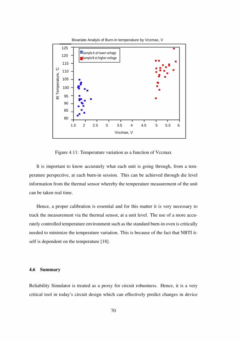
80
115
110
105
100
95
90
85
120
125
BI T
em
pe
ratu
re, ‘C
Vccmax, V
1.5 65.554.543.532.52
Bivariate Analyis of Burn-in temperature by Vccmax, V
Sample A at lower voltage
Sample B at higher voltage
Figure 4.11: Temperature variation as a function of Vccmax
It is important to know accurately what each unit is going through, from a tem-
perature perspective, at each burn-in session. This can be achieved through die level
information from the thermal sensor whereby the temperature measurement of the unit
can be taken real time.
Hence, a proper calibration is essential and for this matter it is very necessary to
track the measurement via the thermal sensor, at a unit level. The use of a more accu-
rately controlled temperature environment such as the standard burn-in oven is critically
needed to minimize the temperature variation. This is because of the fact that NBTI it-
self is dependent on the temperature [18].
4.6 Summary
Reliability Simulator is treated as a proxy for circuit robustness. Hence, it is a very
critical tool in today’s circuit design which can effectively predict changes in device
70

and circuit performance over a product lifetime. It further allows the simulation of
post-degraded circuits to ensure circuit designs meet the reliability requirements at end-
of-life.
The two case studies presented in this chapter were only focusing on voltage and
temperature sensitivities. Based on the simulation done on the on-die thermal sensor
circuit, it is observed that higher voltage and temperature will result in higher NBTI
degradation. Further analysis reported on the specific internal circuit inside the thermal
sensor confirmed as a non-reliability concern because the percentage degradation is
within an acceptable range.
On the other hand, the second case study on the DAC circuit appears to be very
critical due to its high degree of matching requirements. The analysis shows that the
degradation reported on the simulation was much above the typical 2 mV range. This
is due to the stress voltage condition which was set beyond the typical 1.4X nominal
voltage.
In the next chapter, the actual burn-in stress experiment on a specific DAC circuit
was conducted to prove its reliability robustness.
71

CHAPTER 5
BURN-IN STRESS ON DIGITAL-ANALOG-CONVERTER (DAC)
Burn-in stress is one of the key elements in evaluating the reliability robustness of circuit
devices. Therefore, it is very critical to develop a burn-in hardware early enough so that
the experiment can be planned upfront.
In this chapter, a special burn-in experiment on the DAC circuit is described in great
detail. Then, a special burn-in test modes, test patterns as well as special use conditions
are explained. Last but not least, the result of the DAC burn-in experiment is discussed
in section 5.6.
5.1 Introduction
In the previous chapter, the focus was primarily on the analog circuit aging simulations
and their sensitivity across product designs. In order to verify the circuit reliability of
the design, the aim of this chapter is to discuss the burn-in stress that was performed on
the DAC interface.
Reliability and product yield have been playing key roles affecting today’s semi-
conductor manufacturing bottom line [72]. NBTI has emerged as the dominant PMOS
device failure mechanism in the nanometer VLSI era. The extent of NBTI degrada-
tion of a PMOS device increases dramatically at elevated operating temperatures and
supply voltages. Unfortunately, both these conditions are concurrently experienced by

a VLSI chip during the process of burn-in testing. Therefore, burn-in testing can po-
tentially cause significant NBTI degradation of the chip which can require designers to
incorporate reliability mechanisms in their design simulations.
Burn-in stress is an integral part of today’s semiconductor industry back-end test
methodology and is used primarily to screen out the infant mortality regime of the tra-
ditional Bath-tub Failure Rate curve as shown in Figure 5.1. These latent defects or
sometimes called as early life failures are attributable to intrinsic gross faults within
the bought-in components, assembly errors and faults induced in components by inap-
propriate handling such as the ESD damage. Burn-in can reduce the cost of repair by
weeding out potential defective parts before they get assembled into boards. Burn-in
stress is also used for product reliability risk assessment which translates into Defect
Per Million (DPM). This activity refers to early Infant Mortality (IM) fails according to
the first regime of the Bath-tub curve as illustrated in Chapter 2, Figure 2.5.
An extended burn-in or life testing is used to predict long term reliability. These long
term reliability failures are measured in Failure In Time (FIT) rate. It is a measurement
of the number of failures that can be expected in one billion (109) device-hours of
operation. Burn-in is used on rogue or excursion materials to help in risk assessment
and decision making of ship or no-ship of products.
Product defects are accelerated by applying elevated temperature and voltage lev-
els during the burn-in process, while the specified burn-in time (BIT) is optimized to
achieve the outgoing quality goals without significant over stress to the product.
This work does not cover all product burn-in designs or circuit blocks but instead
the focus is only on the DAC interface.
The details of how much voltage stress is required at each circuit node can vary with
products requirements. The classifications of some digital or analog circuits, simply
because they fall within such block boundaries in a design hierarchy, can also cloud the
issue. For example the Double Data Rate (DDR) interface has both digital and analog
circuits. Depending on which design block, the voltage acceleration coverage clearly
74

vary across designs and test methods. Therefore, it is very critical to run thorough circuit
aging simulation since inadequate voltage acceleration coverage is always a possibility
like the DAC circuit.
5.2 DAC Burn-In Conditions
The typical lifetime of a desktop computer or a netbook is less than 7 years [6]. Hence,
the usage conditions are very much important especially for the end users to comply
so that they do not exceed the limits defined by the design specifications. Due to this
requirement, there are design rules developed for the product/process design which are
intended to prevent both the circuit designers and the end-users from over-stressing the
devices. In this context, the focus is on the DAC device.
Failure acceleration is accomplished by two factors, the voltage and the temperature.
Higher junction temperature will accelerate chemical reaction, diffusion defects, and
contamination decomposition while elevating operating voltage will accelerate the gate
oxide defects, particle defects, and Inter-Layer Dielectric (ILD) defects [73].
The Voltage Acceleration Factor equation follows the Arrhenius equation [73] and
is defined by equation (5.1).
VAF = eC(V2−V1) (5.1)
where V2 is the stress VCC at the stress level, V1 is a nominal VCC, and C is a
constant that is technology (gate oxide) dependent.
Temperature Acceleration Factor equation as explained in [73] is defined by equa-
tion (5.2)
TAF = eEa/k∗(1/T 1−1/T 2) (5.2)
75

where:
• Ea is the defect activation energy. The value is typically 0.3 to 1.0 eV, dependingon the defect mechanisms.
• T1 and T2 are the use junction and the stress junction temperature, both in degreeKelvin (C+273)
• k is a Boltzmann constant = 8.617x10⁻⁵ eV/deg K
The total acceleration A between two Voltage/Temp conditions is then the multi-
plicative product of the two factors, as shown in equation (5.3).
A21(i) = eQi/k∗(1/T 1−1/T 2)+Ci(V2−V1) (5.3)
where:
• T2, V2, T1, V1 are operating temperatures (in degree Kelvin) and voltages atconditions 2 and 1, respectively.
• k = 8.61 x 10⁻⁵ eV/K is Boltzmann constant
• Qi (eV) is the thermal activation energy for mechanism i
• Ci (volts-1) is the voltage acceleration constant for mechanism i
In actual fact, separate failure mechanisms may have different acceleration factors
but in practice during the infant mortality baseline generation, composite voltage and
temperature acceleration factors are calculated.
In this work, the voltage supply of interest is the analog CRT DAC power supply,
VCCA. The nominal voltage for this power supply is 3.3V. Table 5.1 shows the cal-
culated acceleration factors using the Arrhenius equation for the device used in this
research.
5.3 DAC Burn-In Stress Test Mode
The standard burn-in method focuses on voltage and temperature as the primary latent
defect accelerants. However, for the purpose of this experiment, the burn-in stress was
76

Table 5.1: Calculated acceleration factors.
Parameters Nominal Conditions Burn In conditions
Voltage (VCCA CRT DAC) 3.3V 4.6V
Temperature 80 100
Burn In Conditions
43095.76
0.24
10357.43
Acceleration Factor
Voltage Acceleration Factor, VAF
Temperature Acceleration Factor, TAF
Total Acceleration Factor, A
run on a special procedure. This new procedure is to implement an on-die clock with
a temperature control diode to speed up the Burn-in test modes. As the frequency
is increased, the internal junction temperature is elevated to meet the required stress
temperature, without raising the surrounding ambient temperature.
During the Burn-In test mode, all clocks will run at 20 MHz as long as the part is
running below a threshold temperature detected by the on-die thermal sensors. This 20
MHz clock is achieved by using two 10 MHz clocks, each 90 degrees phase shifted.
When the thermal sensor detects that the part is too hot, all clocks will slow down to 1
MHz. But when the thermal sensor detects a catastrophic condition, all of the clocks
will be stopped and the part will go into IDDQ (leakage) test mode.
The Burn-in test mode exercises all the basic components of the DAC design (de-
coders, band-gap voltage generator, constant current source, etc.). This test mode
should provide the needed Burn-In toggle coverage on the DAC outputs by producing a
full staircase ramp and the full output voltage swing of 0V to 0.7V on these buffers.
The DAC burn-in Test Mode simply muxes the outputs of an 8-bit counter into the
DACs 8-bit decoders. Thus on a per clock basis the DAC are stepped through all 256
possible digital codes in sequence. This produces a staircase (saw-tooth) waveform
with the DAC Test[3:0] bits in Figure 5.2. All 3 DAC channels will produce a triangle
pattern ranging from code 0 to code 255. This ”triangle” pattern will have an increase of
1 LSB testing both the up and down directions. With this test mode activated, the DAC’s
internal 8-bit up/down counter is enabled and produces a triangular input data pattern.
The waveform will ramp from 00 to FF and then will ramp from FF to 00 hex, which is
77

White Video
Level
(Code 255)
Black
Video
Level
(Code 0)
Status Signal
DAC Digital Input
Code and Outputs
(R, G, B channels)
One pixel
clock
period
Figure 5.1: The pulse width of the status signal of the Burn-In monitor output pin.
muxed to the inputs of all three DAC channels. This operation isl repeated throughout
the whole period of the burn-in operation. This operation provides full burn-in toggle
coverage of the CRT DAC for burn-in testing. As the 8-bit counter reaches its terminal
count value, either FF or 00 hex, a status signal from the video DAC embedded block
transitions. At the completion of the count, the MSB of the counter is sent out through
the Burn-In monitor output pin.
5.4 Burn-In System
Burn-in is an integral part of semiconductor companies back end test methodology and
is used primarily to screen out the infant mortality section of the traditional Bathtub
Failure Rate curve in Figure 5.1.
Product defects are accelerated by applying elevated temperature and voltage levels
during the burn-in process. Typically, the burn-in stress is done by loading the samples
into the burn-in oven utilizing the burn-in boards. During the burn-in operation, the
burn-in oven supplies the elevated voltages to the samples while maintaining the oven
at elevated temperature. The values of the voltage and temperature vary from product
to product due to the nature of the fabrication process technology envelope. During the
burn-in process, the electrical bias applied is either static or dynamic, depending on the
78

failure mechanism being accelerated. However, the burn-in experiment performed on
the DAC interface was run on a special burn-in system.
Just like a TV or cable box at homes heats up when running, this special burn-in sys-
tem relies on the heat-up process to facilitate a self initiated burn-in instead of requiring
an oven. Once the oven is eliminated, traditional batch-based handling equipment can
be streamlined and faster asynchronous continuous flow can be implemented.
The key advantage of this special system is that it can measure silicon stress more
accurately. Working with smaller transistors at higher power and lower voltage required
a new burn-in process. For this specific work, the burn-in equipment was specifically
designed to burn-in test the lower power (0-75 Watt) products that do not require a
specific cooling solution. For this work, the CRT DAC is already part of the device
which has the ability to heat itself up to the desired burn-in test temperature. This
capability is one of the Design-For-Test (DFT) features used for most of Intel products.
The device is capable of regulating and holding its temperature by modulating the speed
of a forced-air cooling fan and the core speed of the device. Hence, this work took the
advantage of the given DFT feature to complete the CRT DAC burn-in activities.
5.5 DAC Burn-In Experiment
Burn-in usually employs exposing the device to extremes of temperature and voltage for
a specified period of time and monitoring the health of the part at Post Burn-In Check
(PBIC). The PBIC test should include a test that checks the DAC burn-in test mode and
a set of tests that check the DACs functionality. Due to the ATE tester limitations, it
would be difficult to create a test that has enough resolution that could detect minor
variations in the DAC performance induced by the burn-in.
This burn-in experiment is not meant to screen out the infant mortality behavior.
Instead, the main purposes of this experiment are the following:
79

• To ensure no product specific issues which could show a high risk parametric shift
(Example : Pin signal is out of specification or new circuitry with critical timings
is not being checked on or prior to the productions)
• To ensure the product design follow all design rules for that particular fabrication
process.
• To provide a measure of device reliability and Negative Bias Temperature Insta-
bility degradation (NBTI) concern.
• To ensure the outgoing quality is within the specification limit throughout the
product life cycle.
For a specific DAC burn-in experiment, 300 units from 3 fabrication lots were run
through the experimental flow whereby the wafers were then sent into assembly die
inventory (ADI) where it waited for the final assembly and testing. The overall Burn-In
experimental flow is illustrated in Figure 5.3.
The Raw Class 1 (RC1) is a high temperature test. The main objective of doing raw
class testing is to screen out assembly related defects. Next, these units were subjected
to burn-in stress for 30 minutes and completed by Post Burn-In Check (PBIC). Similar
process took place until all units completed the cumulative 168-hour burn-in. The main
purpose of this work is not looking at these 300 experimental units but rather to sample
out 25 good units for a specific DAC burn-in characterization. Out of all 25 units, 1
unit from each fabrication lot was marked separately to be treated as the control unit.
The idea was that these control units are to be tested first and the data to be taken in a
separate log file for comparison purposes, while the rest of the units will be tested after
each of the burn-in readouts at a hot temperature of 115C.
With regards to the test contents of the ATE testers, a series of electrical measure-
ments (timing and parametric shift) are taken at different stages. A total of 25 good
units from 3 qualification lots will incur burn-in stress for 12 cumulative hours with
readouts taken at time zero, 30 minutes, and 12 cumulative hours. The readouts will
80

Material Selection
Hot Raw Class (115 ’C)
Sort/Assembly
Hot test 115C
Test completed
(no burn-in)
This is time zero read- out
and control units
identification
Material Selection
’C)
Sort/Assembly
0.5 hrs cumulative burn-in(95C, 4.6V)
Hot test 115C
Test completed
Control unit
This is time zero read- out
and control units
identification Sample out 25 units ( 5 units/lot) and mark 1 each as control unit
Hot test 115C
(no burn-in) 12 hrs cumulative burn-in(95C, 4.6V)
Hot test 115C
Control unit
Hot test 115C
(no burn-in) 18 hrs cumulative burn-in(95C, 4.6V)
Hot test 115C
Control unit
Hot test 115C
(no burn-in) 48 hrs cumulative burn-in(95C, 4.6V)
Hot test 115C
Control unit
Hot test 115C
(no burn-in) 168 hrs cumulative burn-in(95C, 4.6V)
Hot test 115C
Control unit
Figure 5.2: DAC Burn-In Experimental Flow.
consist of AC and DC testing with pins and parameters chosen to provide test coverage
to all buffers and pin types.
The aim of the test results is to collect data based on the following parameters:
• Differential Non-Linearity (DNL)
• Integral Non-Linearity (INL)
• Gain Error
• Offset Error
• Output Current
81

Figure 5.3: DAC burn-in comparison, 3.3V vs 4.6V
5.6 DAC Burn-In Result
Figure 5.4 summarizes the DAC burn-in result. The work was conducted on two legged
burn-in experiment. The first leg was run under nominal voltage of 3.3V while the
second leg was done under elevated burn-in voltage of 4.6V. Based on the graph plotted,
it clearly shows that the higher voltage difference between gate and source will result
in a higher degradation.
As explained in the theory in Section 2.2.1.1, this is a result of the higher oxide
electric field causing a larger number of interface traps. Oxide electric field enhances
NBTI. NBTI is very sensitive to electric field as shown in the Figure 5.5, in terms of the
applied gate voltage for two different oxide thicknesses [5]. According to Ogawa et al.
the interface trap and fixed charge generation show an Eox1.5 dependence [74]. NBTI
performance is judged by the extrapolating time-to-failure (TTF) to a typical percentage
of parameter shift.
TTF is a function of the following:
• Vstress (↑ means ↓ TTF)
82

Figure 5.4: Lifetime as a function of gate voltage. Data after Schroder et al.[5].
Table 5.2: Summary of 168 hours (7 years) Burn-In experiment of DAC
Items Pre Burn-In Post Burn-In Percent Change
DNL mean 0.185 LSB 0.197 LSB 6.48%
INL mean 0.235 LSB 0.246 LSB 4.68%
Gain Error 3.585V 2.500V 43.50%
Offset Error 0.000344V 0.000361V 4.90%
Output Current 59 mA 60.2 mA 2%
• Vcc - Vt (↑ means ↓ TTF)
DAC or even ADC are the key components of data-acquisition systems. They act as
communication blocks for both analog and digital blocks [11]. In principle, when the
digital input is given to a DAC, it will provide an accurate output voltage. In practice,
the accuracy of the output voltage is subject to the offset and the gain errors from the
DAC building block and other devices in the signal chain. Hence, in order to verify
the robustness of the DAC performance after burn-in stress, the key DAC parameters,
which are critical to extreme matching are measured. These measurements were taken
after the last burn-in readout of 168-hours under a severe stress condition of 4.6V. The
key test results measured before and after the burn-in stress are summarized in Table
5.2.
Based on the test results measured, the gain error measurement after the post burn-
in stress was the only parameter that has a significant spike as compared to the rest of
83

Table 5.3: The Vout data taken before and after Burn-In stress
Input code Vout @ pre Burn-In Vout @ post Burn-In
0 0.000 0.000
1 0.167 0.239
2 0.333 0.478
3 0.500 0.717
4 0.667 0.956
5 0.833 1.195
6 1.000 1.434
7 1.167 1.673
8 1.333 1.912
9 1.500 2.151
10 1.667 2.390
11 1.833 2.629
12 2.000 2.868
13 2.167 3.107
14 2.333 3.346
15 2.500 3.585
the key parameters. A significant increase in the gain error of 43.5% was observed. The
ideal situation is that the DAC’s gain error has to be zero. The gain measurement was
collected on the ATE tester. The pre burn-in is assumed to be an ideal case with zero
gain error. Table 5.3 shows that as the DAC input code increases, the output voltage
increases accordingly to 2.5V (Vref).
The post burn-in Vout was measured at the ATE tester and the Vout values increased
by ∼43.5% compared to the typical gain error percentage of less than ∼20%. The gain
was calculated as Av= 3.585/2.5 = ≈1.43406667. Hence, the gain error percentage is
≈43.5%. Figure 5.6 shows the DAC transfer functions of ideal (pre burn-in) vs actual
DAC (post burn-in).
In this specific case, the gain error has created a span greater than the desired ideal
case. The transfer function is modeled as a typical straight line as commonly described
by y = mx + c equation, where:
• y is the output of the DAC
• m is the slope of the transfer function
• x is the input of the DAC
84

DAC OUTPUT vs CODE
0.000
0.500
1.000
1.500
2.000
2.500
3.000
3.500
4.000
1 2 3 4 5 6 7 8 9 10 11 12 13 14 15 16
DAC CODE
VO
UT Vout @ pre Burn-In
Vout @ post Burn-In
Gain Error = ~43.5%
Figure 5.5: DAC characteristic showing an excessive gain error of 43.5%
• c is the offset voltage
Typically, an ideal DAC has a gain, m, of 1 and an offset, c, of 0 and hence the
output tracks the input in a precise linear manner. However, for the real DAC, it has
non-ideal gain and offset values which normally can be compensated once the values
are determined.
For the data taken in this burn-in experiment, the design is based on an 8-bit DAC
with a 0V to 2.5V nominal output span. When the digital input is set to a full scale, a
3.585V output is measured.
From this data, the actual gain error, measured in percentage, can be determined
by multiplying the output voltage at post burn-in by the output voltage at pre burn-in,
3.585V/2.5V = ≈1.43406667. The gain error is calculated with the assumption that the
offset error is zero while the span error is measured at 850 mV, giving an actual span of
3.585V.
85

ASC ACTIVE
EXPECT
MONITOR
Figure 5.6: DAC Output signal during burn-in.
5.7 Correlation of Simulation and Experimental Work
To validate the actual performance of the CRT DAC design, a customized burn-in
hardware was developed to specifically stress the CRT DAC components only. Burn-in
is usually run at a low frequency, 20 MHz. The burn in test mode exercises all the
basic components of the DAC design such as the decoders, band-gap voltage generator,
constant current sources etc. This test mode should provide the needed toggle coverage
on the DAC outputs by producing a full staircase ramp and the full output voltage swing
of 0V to 0.7V on these buffers.
Data shown here was taken on the burn-in board (BIB) at VCC = 4.6V (burn-in
voltage for DAC) with device case temperature of 95C and driver data rate of 20 MHz.
The DAC BIST output can be seen on the monitor output signal (MONITOR) of each
device. Figure 7 shows a small section of the DAC output seen on MONITOR. Auto
Signal Check (ASC) is active twice during this section and is looking for one high
and one low. Since the MONITOR and the EXPECT (simulation data) match while
ASC is active, Auto Signal Check will pass. MONITOR can be found on the rear edge
connector of the BIB. ASC active and expect can be found on test turrets towards the
rear of the BIB.
86

DAC-BIST
RED
800 mV
2V/div
20us/div
-19.7V
25.3236ms 25.5236ms
t1= 25.34 msT2= 25.39 mst = 50.80 us1/ t = 19.68 kHz
25.34 ms 25.39 ms
Figure 5.7: RGB Output signal during burn-in.
Figure 8 shows a screen capture of the monitor output during DAC BIST, and the
output of one of the RGB pins. The RGB outputs can be found on the 3 socket resistors
comprised of Red (pictured below), Green, and Blue.
5.8 Summary
In a nutshell, burn-in stress is one of the key elements to verify circuit reliability specif-
ically the analog devices/circuits.
A special burn-in condition which includes its test modes, test patterns, and use
conditions were set-up. The data after the burn-in stress was collected and compared
with the pre-stress data.
Due to the sensitivity of the DAC functionality, some key DAC parameters were
monitored and compared between pre and post stress. It is observed that a gain error is
the only parameter which is susceptible to elevated use conditions.
The last chapter comprises two sections. Section 6.1 gives the conclusion of this
work and Section 6.2 proposes ideas for future work.
87


CHAPTER 6
CONCLUSIONS AND FUTURE WORK
Developing an efficient reliability simulator covering Process, Voltage and Temperature
variations (PVT) is deemed compulsory in order to deliver highly reliable products in
the SOC business where less customer complaints related to reliability are expected.
To take the leading role in technology and market without sacrificing reliability, circuit
designers must be equipped with accurate reliability modeling and simulation tools to
help control the reliability from the very beginning design stage to the final qualification.
The main objective of this work is to study the NBTI failure mechanism and its
sensitivity in the two critical analog devices, comparing the aging simulation result to
the actual burn-in experiment.
This last chapter comprises two sections. Section 6.1 provides the conclusion of
this work and Section 6.2 gives an overview of the future work related to this paper.
6.1 Conclusion
As discussed in Section 2.2.1, the NBTI failing mechanism in specific analog circuit
blocks particularly the DAC can cause errors. For this work, specific SOC analog cir-
cuits have been thoroughly investigated, verified and found some important issues in
relation to the NBTI issues.
The work can be separated into 2 main sections.

6.1.1 Voltage and temperature variation in NBTI Model for Circuit Design
Previous work on the NBTI effect to the analog circuits has given some general
ideas on the impact to the circuit performance at different operating conditions. Run-
ning reliability simulation across PVT is mandatory to ensure all process corners and
conditions are fully validated and verified.
This work has been successfully conducted by comparing the simulation result to
the actual silicon performance. However, the interest of the work is to look only at
voltage and temperature sensitivities. Simulation results on both case studies depend
on the nature of the NBTI event.
For example, the on-die thermal sensor simulation results revealed that the NBTI
degradation observed based on the simulation analysis has proven to be non-significant
to cause an error to the thermal sensor functionality. This initial finding of this work
titled ”A case study for reliability-aware in SOC analog circuit design” was presented
as an oral presentation in IEEE International Conference on Intelligent and Advanced
Systems (ICIAS) conducted in Kuala Lumpur in June 2010.
The second case study on the DAC shows a different result. This is due to the higher
degree of matching accuracy required for the DAC to perform at its design specifica-
tion. The NBTI degradation observed in the simulation analysis revealed that under a
severe stress condition like 40% increase in the nominal voltage supply, a significant
voltage threshold mismatch of beyond the 2mV limit was recorded. This work with
the title ”NBTI-induced 8-Bit DAC circuit mismatch in System-On-Chip (SOC)” was
presented as an oral presentation in IEEE 3rd Asia Symposium on Quality Electronic
Design (AsQED) held in Kuala Lumpur in July 2011.
6.1.2 A special Burn In experiment looking into NBTI reliability sensitivity
A burn-in experiment was performed to verify the reliability sensitivity of the DAC
design. Burn-in stress plays an important role in verifying the robustness of circuit
90

design. A defect after burn-in stress can cause performance degradation and can slow
down the circuit operation.
Through this special burn-in experiment on the DAC circuit, it is proven that ele-
vating both voltage and temperature at the extreme conditions can cause critical DAC
parameters to be malfunctioned. In this case, the voltage was elevated to 1.4X nominal
supply voltage while the temperature was set at 90-100C. The gain error was deter-
mined to be at the upper extreme reading, 43.5% to be exact.
In summary, the reliability simulation demonstrated a shift of the threshold voltage,
Vt on the CRT DAC specifically at the current source array component, implying the
existence of NBTI mechanism. Correlations between reliability simulations and the
burn-in systems were attempted, which are critical in characterizing the key components
of the DAC design specifically the current source array circuit. This attempt provides
high confidence in the reliability model and the simulation developed. As a result,
the actual burn-in stress conducted on the CRT DAC shows variations in the biasing
currents due to NBTI, which resulted in a gain error. This paper sheds some light for the
next generation SOC products to perform an accurate reliability simulation modeling
and to correlate with burn-in systems in order to minimize reliability induced mismatch.
NBTI is one of the most important sources of failures affecting transistors. The
question that may arise is that what needs to be done once NBTI effects are known.
Some possible methods are introduced to reduce the effect of NBTI.
1. Simulation - This method, as discussed in this thesis, mitigates NBTI by running
circuit level simulation using AgingSim to verify the NBTI impact. By running
AgingSim, the outlier of the NBTI paths can be fixed real time.
2. Test Guardband - This method mitigates NBTI by introducing a fixed percentage
of the maximum frequency (Fmax) buffer between the test and the usage fre-
quency (i.e. test at 3.4 GHz, higher than the specification frequency of 3.2Ghz).
In addition to this method, some investments need to be put on the table. As the
mean and the sigma of NBTI percentage increases, more Fmax buffer is needed.
91

3. Aging heuristics - This method mitigates NBTI by applying delay penalty to com-
pensate for circuits with higher NBTI percentage. By using heuristics, time can
be reduced when solving problems. At the same time, this method ensures good
design practice.
4. Dynamic VCC and Bus-ratio adjustment - This method is still under feasibility
study. The method adjusts the dynamic VCC and the bus-ratio during the us-
age conditions based on the Intra-Die Variation Probe (IDVP) degradation as an
indicator.
6.2 Future Work
Since this paper has focused on the voltage and the temperature effect to the NBTI
event, the future work will be focusing on the effect of process variation. Some initial
works have started and the work title ”IDVP (Intra-Die Variation Probe) for System-
on-Chip (SOC) Infant Mortality Screen” has been presented as an oral presentation in
the IEEE International Symposium on Circuits and Systems (ISCAS) which was held in
Rio de Janeiro, Brazil in May 2011. Another work, which is also related to the process
variation effect, titled ”A Case Study of Process Variation Effect to SOC Analog Cir-
cuits” has been published in the IEEE Recent Advances in Intelligent Computational
Systems (RAICS) which was held in Trivandrum, India in September 2011.
Recent sub-micron process technology scaling leads the urgency to build an efficient
methodology of characterizing and modeling the process variation effect, for example,
the threshold voltage, Vt. This is one of the key process parameters that must be ex-
tensively modeled and validated for accurate circuit performance. Furthermore, this
requirement is even more critical for analog applications which demand an ability to
match devices precisely.
92

REFERENCES
[1] K. Arendt, “Private communication.” Intel Corporation, 2009.
[2] R. Tu, E. Rosenbaum, W. Chan, C. Li, E. Minami, K. Quader, P. Ko, and C. Hu,
“Berkeley reliability tools,” IEEE Transactions on Computer-Aided Design of In-
tegrated Circuits and Systems, vol. 12, pp. 1524 –1534, Oct. 1993.
[3] S. Nassif, N. Mehta, and Y. Cao, “A resilience roadmap,” in Design, Automation
Test in Europe Conference Exhibition (DATE), 2010, pp. 1011 –1016, march 2010.
[4] H. Kufluoglu, V. Reddy, A. Marshall, J. Krick, T. Ragheb, C. Cirba, A. Krish-
nan, and C. Chancellor, “An extensive and improved circuit simulation method-
ology for nbti recovery,” in IEEE International on Reliability Physics Symposium
(IRPS), pp. 670 –675, may 2010.
[5] D. K. Schroder and J. A. Babcock, “Negative bias temperature instability: Road
to cross in deep submicron silicon semiconductor manufacturing,” Journal of Ap-
plied Physics, vol. 94, pp. 1 –18, July 2003.
[6] N. Jha, P. Reddy, D. Sharma, and V. Rao, “Negative bias temperature instability
degradation and its impact for analog circuit reliability,” IEEE Transactions on
Electron Devices, vol. 52, no. 12, pp. 2609 – 2615, 2005.
[7] X. Li, J. Qin, and J. Bernstein, “Compact modeling of mosfet wearout mechanisms
for circuit-reliability simulation,” IEEE Transactions on Device and Materials Re-
liability, vol. 8, no. 1, pp. 98 –121, 2008.
93

[8] B. Yan, Q. Fan, J. Bernstein, J. Qin, and J. Dai, “Reliability simulation and circuit-
failure analysis in analog and mixed-signal applications,” vol. 9, pp. 339 –347,
2009.
[9] S. Kumar, K. Kim, and S. Sapatnekar, “Impact of nbti on sram read stability and
design for reliability,” in 7th International Symposium on Quality Electronic De-
sign (ISQED), pp. 6 pp. –218, march 2006.
[10] V. Huard, C. Parthasarathy, A. Bravaix, T. Hugel, C. Guerin, and E. Vincent,
“Design-in-reliability approach for nbti and hot-carrier degradations in advanced
nodes,” IEEE Transactions on Device and Materials Reliability, vol. 7, pp. 558
–570, dec. 2007.
[11] P. Nicollian, W. Hunter, and J. Hu, “Experimental evidence for voltage driven
breakdown models in ultrathin gate oxides,” in 38th Annual IEEE International
Reliability Physics Symposium, 2000.
[12] T. Tomita, H. Utsunomiya, T. Sakura, Y. Kamakura, and K. Taniguchi, “A new
soft breakdown model for thin thermal sio2 films under constant current stress,”
IEEE Transactions on Electron Devices, vol. 46, pp. 159 –164, Jan. 1999.
[13] M. Alam, B. Weir, and P. Silverman, “A study of soft and hard breakdown - part
i: Analysis of statistical percolation conductance,” IEEE Transactions on Electron
Devices, vol. 49, pp. 232 –238, Feb. 2002.
[14] A. Kerber, E. Cartier, R. Degraeve, P. Roussel, L. Pantisano, T. Kauerauf, G. Groe-
seneken, H. Maes, and U. Schwalke, “Charge trapping and dielectric reliability of
sio2-al2o3 gate stacks with tin electrodes,” IEEE Transactions on Electron De-
vices, vol. 50, pp. 1261 – 1269, May 2003.
[15] M. Ball, J. Rosal, R. McKee, W. Loh, T. Houston, R. Garcia, J. Raval, D. Li,
R. Hollingsworth, R. Gury, R. Eklund, J. Vaccani, B. Castellano, F. Piacibello,
S. Ashburn, A. Tsao, A. Krishnan, J. Ondrusek, and T. Anderson, “A screening
94

methodology for vmin drift in sram arrays with application to sub-65nm nodes,”
in International Electron Devices Meeting (IEDM), pp. 1 –4, dec. 2006.
[16] A. Sedra and K. Smith, Microelectronic Circuits. New York: Oxford University
Press, third ed., 1991.
[17] M. Agostinelli, S. Lau, S. Pae, P. Marzolf, H. Muthali, and S. Jacobs, “Pmos
nbti-induced circuit mismatch in advanced technologies,” in 42nd Annual IEEE
Internationa Reliability Physics Symposium Proceedings, pp. 171 – 175, 2004.
[18] N. Kimizuka, K. Yamaguchi, K. Imai, T. Iizuka, C. Liu, R. Keller, and T. Horiuchi,
“Nbti enhancement by nitrogen incorporation into ultrathin gate oxide for 0.10-
mu;m gate cmos generation,” in Digest of Technical Papers, VLSI Technology,
2000.
[19] Y.-H. Lee, N. Mielke, B. Sabi, S. Stadler, R. Nachman, and S. Hu, “Effect of
pmost bias-temperature instability on circuit reliability performance,” in IEEE In-
ternational Conference on Electron Devices Meeting, pp. 14.6.1 – 14.6.4, 2003.
[20] J. Martin-Martinez, R. Rodriguez, M. Nafria, and X. Aymerich, “Time-dependent
variability related to bti effects in mosfets: Impact on cmos differential amplifiers,”
IEEE Transactions on Device and Materials Reliability, vol. 9, no. 2, pp. 305 –
310, 2009.
[21] S. Mahapatra, V. Maheta, A. Islam, and M. Alam, “Isolation of nbti stress gener-
ated interface trap and hole-trapping components in pno p-mosfets,” IEEE Trans-
actions on Electron Devices,, vol. 56, no. 2, pp. 236 –242, 2009.
[22] W. Evans and D. Burnell, “Deep submicron effects on data converter building
blocks,” in IEEE Custom Integrated Circuits Conference, pp. 725 –728, 2008.
[23] V. Reddy, J. Carulli, A. Krishnan, W. Bosch, and B. Burgess, “Impact of nega-
tive bias temperature instability on product parametric drift,” in International Test
Conference, pp. 148 – 155, 2004.
95

[24] P. Chaparala, D. Brisbin, and J. Shibley, “Nbti in dual gate oxide pmosfets,” in 8th
International Symposium Plasma- and Process-Induced Damage, pp. 138 – 141,
2003.
[25] G. Chen, M. Li, C. Ang, J. Zheng, and D. Kwong, “Dynamic nbti of p-mos tran-
sistors and its impact on mosfet scaling,” IEEE Electron Device Letters, vol. 23,
pp. 734 – 736, Dec. 2002.
[26] A. Ghosh, R. Franklin, and R. Brown, “Analog circuit design methodologies to
improve negative-bias temperature instability degradation,” in 23rd International
Conference on VLSI Design, pp. 369 –374, 2010.
[27] B. Greskamp, S. Sarangi, and J. Torrellas, “Threshold voltage variation effects
on aging-related hard failure rates,” in IEEE International Symposium on Circuits
and Systems, pp. 1261 –1264, May 2007.
[28] E. Maricau and G. Gielen, “A methodology for measuring transistor ageing ef-
fects towards accurate reliability simulation,” in 15th IEEE International On-Line
Testing Symposium, pp. 21 –26, 2009.
[29] K. Rafeeque and V. Vasudevan, “A new technique for on-chip error estimation
and reconfiguration of current-steering digital-to-analog converters,” IEEE Trans-
actions on Circuits and Systems I: Regular Papers, vol. 52, no. 11, pp. 2348 –
2357, 2005.
[30] M. Singh and I. Koren, “Fault-sensitivity analysis and reliability enhancement of
analog-to-digital converters,” IEEE Transactions on Very Large Scale Integration
(VLSI) Systems, vol. 11, no. 5, pp. 839 – 852, 2003.
[31] L. Lewyn, T. Ytterdal, C. Wulff, and K. Martin, “Analog circuit design in
nanoscale cmos technologies,” Proceedings of the IEEE, vol. 97, no. 10, pp. 1687
–1714, 2009.
96

[32] S. K. Krishnappa, H. Singh, and H. Mahmoodi, “Incorporating effects of process,
voltage, and temperature variation in bti model for circuit design,” pp. 236 –239,
feb. 2010.
[33] C. Parthasarathy, M. Denais, V. Huard, G. Ribes, E. Vincent, and A. Bravaix,
“Characterization and modeling nbti for design-in reliability,” in IEEE Interna-
tional Integrated Reliability Workshop Final Report, p. 5 pp., 2005.
[34] H. Luo, Y. Wang, K. He, R. Luo, H. Yang, and Y. Xie, “Modeling of pmos nbti ef-
fect considering temperature variation,” in 8th International Symposium on Qual-
ity Electronic Design, pp. 139 –144, 2007.
[35] W. Wang, S. Yang, S. Bhardwaj, S. Vrudhula, F. Liu, and Y. Cao, “The im-
pact of nbti effect on combinational circuit: Modeling, simulation, and analysis,”
IEEE Transactions on Very Large Scale Integration (VLSI) Systems, vol. 18, no. 2,
pp. 173 –183, 2010.
[36] B. Zhang and M. Orshansky, “Modeling of nbti-induced pmos degradation un-
der arbitrary dynamic temperature variation,” in 9th International Symposium on
Quality Electronic Design, pp. 774 –779, 2008.
[37] B. Yan, J. Yang, Z. Xia, X. Liu, G. Du, R. Han, J. Kang, C. Liao, Z. Gan, M. Liao,
J. Wang, and W. Wong, “Anomalous negative bias temperature instability degrada-
tion induced by source/drain bias in nanoscale pmos devices,” IEEE Transactions
on Nanotechnology, vol. 7, no. 4, pp. 418 –421, 2008.
[38] C. Guardiani, A. Shibkov, A. Brambilla, G. Gajani, D. Appello, F. Piazza, and
P. Bernardi, “An i-ip based approach for the monitoring of nbti effects in socs,” in
15th IEEE International On-Line Testing Symposium, pp. 15 –20, 2009.
[39] H.-C. Lin, D.-Y. Lee, S.-C. Ou, C.-H. Chien, and T.-Y. Huang, “Impacts of hole
trapping on the nbti degradation and recovery in pmos devices,” in Extended Ab-
stracts of International Workshop on Gate Insulator, pp. 76 – 79, 2003.
97

[40] J. Keane, T.-H. Kim, and C. Kim, “An on-chip nbti sensor for measuring pmos
threshold voltage degradation,” IEEE Transactions on Very Large Scale Integra-
tion (VLSI) Systems, vol. 18, no. 6, pp. 947 –956, 2010.
[41] B. Razavi, Design of Analog CMOS Integrated Circuits. Boston: McGraw-Hill,
international ed., 2001.
[42] D. Duarte, G. Geannopoulos, U. Mughal, K. Wong, and G. Taylor, “Temperature
sensor design in a high volume manufacturing 65nm cmos digital process,” in
IEEE Custom Integrated Circuits Conference, pp. 221 –224, 2007.
[43] H. Banba, H. Shiga, A. Umezawa, T. Miyaba, T. Tanzawa, S. Atsumi, and
K. Sakui, “A cmos band-gap reference circuit with sub 1 v operation,” in VLSI
Circuits Symposium, pp. 228 –229, jun 1998.
[44] A. van Roermund, H. Hegt, P. Harpe, G. Radulov, A. Zanikopoulos, K. Doris,
and P. Quinn, “Smart ad and da converters,” in IEEE International Symposium on
Circuits and Systems, pp. 4062 – 4065 Vol. 4, May 2005.
[45] I. A. Devices, Analog-Digital Conversion Handbook. Englewood Cliffs, New
Jersey: Prentice-Hall, international ed., 1986.
[46] J. Bastos, A. Marques, M. Steyaert, and W. Sansen, “A 12-bit intrinsic accuracy
high-speed cmos dac,” IEEE Journal of Solid-State Circuits, vol. 33, pp. 1959
–1969, Dec. 1998.
[47] C.-Y. Huang, T.-T. Hou, C.-C. Chuang, and H.-Y. Wang, “Design of 12-bit 100-
mhz current-steering dac for soc applications,” in Fifth International Workshop on
System-on-Chip for Real-Time Applications, pp. 117 – 122, 2005.
[48] J.-S. Wang and C.-L. Wey, “High-speed cmos switched-current d/a converters
for low-power/low-voltage signal processing applications,” in IEEE International
Conference on Electronics, Circuits and Systems, 1998.
98
[49] K. Deguchi, N. Suwa, M. Ito, T. Kumamoto, and T. Miki, “A 6-bit 3.5-gs/s 0.9-v
98-mw flash adc in 90nm cmos,” in IEEE Symposium on VLSI Circuits, pp. 64
–65, 2007.
[50] A. Bakker and J. Huijsing, “Micropower cmos smart temperature sensor,” in
Twenty-first European Solid-State Circuits Conference, pp. 238 –241, 1995.
[51] J. Dorsey, S. Searles, M. Ciraula, S. Johnson, N. Bujanos, D. Wu, M. Braganza,
S. Meyers, E. Fang, and R. Kumar, “An integrated quad-core opteron processor,”
in IEEE International Conference on Solid-State Circuits (ISSCC), pp. 102 –103,
2007.
[52] V. Gupta and G. Rincon-Mora, “Predicting and designing for the impact of process
variations and mismatch on the trim range and yield of bandgap references,” in
Sixth International Symposium on Quality of Electronic Design, pp. 503 – 508,
2005.
[53] V. Gupta and A. Rincon-Mora, “Predicting the effects of error sources in bandgap
reference circuits and evaluating their design implications,” in 45th Midwest Sym-
posium on Circuits and Systems, vol. 3, pp. III–575 – III–578 vol.3, aug. 2002.
[54] M.-D. Ker, J.-S. Chen, and C.-Y. Chu, “A cmos bandgap reference circuit for sub-
1-v operation without using extra low-threshold-voltage device,” in International
Symposium on Circuits and Systems, vol. 1, pp. I–41 – I–44 Vol.1, May 2004.
[55] D.-Y. Chang and S.-H. Lee, “Design techniques for a low-power low-cost cmos
a/d converter,” IEEE Journal of Solid-State Circuits, vol. 33, pp. 1244 –1248, aug
1998.
[56] A. Ab-Rahman and I. Kamisian, “Analysis on the effects of mosfet threshold volt-
age mismatch in cmos operational amplifiers for rf applications,” in International
RF and Microwave Conference, pp. 192 –196, sept. 2006.
99
[57] C. Enz and G. Temes, “Circuit techniques for reducing the effects of op-amp im-
perfections: autozeroing, correlated double sampling, and chopper stabilization,”
Proceedings of the IEEE, vol. 84, pp. 1584 –1614, nov 1996.
[58] D. Lorenz, G. Georgakos, and U. Schlichtmann, “Aging analysis of circuit timing
considering nbti and hci,” in 15th IEEE International On-Line Testing Symposium,
pp. 3 –8, 2009.
[59] K. Skadron, M. Stan, W. Huang, S. Velusamy, K. Sankaranarayanan, and D. Tar-
jan, “Temperature-aware microarchitecture,” in 30th Annual International Sympo-
sium on Computer Architecture, pp. 2 – 13, june 2003.
[60] J. B. Bernstein, M. Gurfinkel, X. Li, W. J, Y. Shapira, and M. Talmor, “Electronic
circuit reliability modeling,” Microelectronics Reliability, vol. 46, pp. 1957 –1979,
2006.
[61] Reliasoft, “Limitations of the exponential distribution for reliability analysis,”
2001. Reliability Edge Newsletter.
[62] V. Szekely, C. Marta, Z. Kohari, and M. Rencz, “Cmos sensors for on-line thermal
monitoring of vlsi circuits,” IEEE Transactions on Very Large Scale Integration
(VLSI) Systems, vol. 5, pp. 270 –276, sept. 1997.
[63] M. Pertijs, A. Niederkorn, X. Ma, B. McKillop, A. Bakker, and J. Huijsing, “A
cmos smart temperature sensor with a 3σ; inaccuracy of ±0.5c from -50c to
120c,” IEEE Journal of Solid-State Circuits, vol. 40, no. 2, pp. 454 – 461, 2005.
[64] G. Meijer, G. Wang, and F. Fruett, “Temperature sensors and voltage references
implemented in cmos technology,” IEEES sensors Journal, vol. 1, pp. 225 –234,
Oct. 2001.
[65] Y. Nishida, H. Sayama, K. Ohta, H. Oda, M. Katayama, Y. Inoue, H. Morimoto,
and A. Inuishi, “Soc cmos technology for nbti/hci immune i/o and analog circuits
100

implementing surface and buried channel structures,” in International Electron
Devices Meeting, 2001.
[66] A. Syal, V. Lee, I. Andre, and J. Altet, “Cmos differential and absolute thermal
sensors,” in Seventh International On-Line Testing Workshop, 2001.
[67] Y. Kilic and M. Zwolinski, “Process variation independent built-in current sensor
for analogue built-in self-test,” in IEEE International Symposium on Circuits and
Systems, vol. 4, pp. 398 –401 vol. 4, May 2001.
[68] L. Zhang and R. Dick, “Scheduled voltage scaling for increasing lifetime in
the presence of nbti,” in Asia and South Pacific Design Automation Conference,
pp. 492 –497, 2009.
[69] C. A. Poynton, Digital video and HDTV : algorithms and interfaces. Morgan
Kaufmann series in computer graphics and geometric modeling, Morgan Kauf-
mann Publishers, 1st ed., 2003.
[70] E. Ozalevli, H.-J. Lo, and P. Hasler, “Binary-weighted digital-to-analog converter
design using floating-gate voltage references,” IEEE Transactions on Circuits and
Systems I: Regular Papers, vol. 55, pp. 990 –998, May 2008.
[71] A. Srivastava, S. Yellampalli, and K. Golla, “Delta-iddq testing of a cmos 12-bit
charge scaling digital to analog converter,” in 49th IEEE International Midwest
Symposium on Circuits and Systems, vol. 1, pp. 443 –447, 2006.
[72] V. Parihar, R. Singh, and K. Poole, “Silicon nanoelectronics: 100 nm barriers
and potential solutions,” in IEEE/SEMI Advanced Semiconductor Manufacturing
Conference and Workshop, pp. 427 –433, Sept. 1998.
[73] M. Zakaria, Z. Kassim, M.-L. Ooi, and S. Demidenko, “Reducing burn-in time
through high-voltage stress test and weibull statistical analysis,” IEEE Design Test
of Computers, vol. 23, no. 2, pp. 88 – 98, 2006.
101

[74] S. Ogawa, M. Shimaya, and N. Shiono, “Interface-trap generation at ultrathin sio2
(46 nm)- si interfaces during negative bias temperature aging,” Journal of Applied
Physics, vol. 77, pp. 1137 –1148, feb. 1995.
102

LIST OF PUBLICATION
The research work in this thesis was presented and published in official proceedings
of rigorously referred conferences through the following research papers:
1. Abdul Latif, M.A., Zain Ali, N.B., Hussin, F.A. ”A Case Study for Reliability-
Aware in SOC Analog Circuit Design,” In IEEE International Conference on
Intelligent and Advanced Systems (ICIAS), Kuala Lumpur, June 2010.
2. Abdul Latif, M.A., Zain Ali, N.B., Hussin, F.A. ”IDVP (Intra-Die Variation
Probe) for System-on-Chip (SOC) Infant Mortality Screen,” In IEEE Inter-
national Symposium on Circuits and Systems (ISCAS), Rio De Janeiro, Brazil,
May 2011.
3. Abdul Latif, M.A., Zain Ali, N.B., Hussin, F.A. ”NBTI-induced 8-Bit DAC
Circuit Mismatch in System-On-Chip (SOC),” In IEEE Asia Symposium on
Quality Electronic Design (ASQED), Kuala Lumpur, July 2011.
4. Abdul Latif, M.A., Zain Ali, N.B., Hussin, F.A. ”A Case Study of Process Vari-
ation Effect to SOC Analog Circuits,” In IEEE Recent Advances in Intelligent
Computational Systems (RAICS), Trivandrum, India, September 2011.
103

APPENDIX A
DAC BURN-IN PLAN
The burn-in board matrix is customized specifically to stress the DAC circuit. The
original intent of building the burn-in board was to use for a specific product sample
but for this special experiment, the emphasis is on stressing the DAC circuit. Trace
impedance of all channels is controlled to allow operation of the signals operating at 10
MHz, low frequency. The output monitor signal (DAC out) is to be brought out to the
burn-in board edge connector for the BI socket through a 100 ohm series resistor. The
purpose is to facilitate the debug of DAC burn-in.
This special DAC BI is structurally exercised with DAC power supply at elevated
voltage of 4.6V (VCC DAC). Other power supplies which are not to the interest of this
experiment are core power supplies at 1.6V (VCC Core) and I/O power supplies at 2.5V
(VCC I/O) The reference voltages are set to 1/2 VTT, 1/2 VDD, or 2/3 VCC depending
on the interfaces. A dedicated burn-in system supply is used for the 4.6V source. A
resistor divider is used to acquire proper reference source. The BI frequency under BI
mode is 10 MHz. Each of the product samples is laid to support single voltage supply
requirement.
A series of inexpensive discrete components is mounted on a burn-in board (BIB)
to stimulate, and monitor a new on-die burn-in stress mode for DAC. This is to make
each burn-in board a self-contained independent stress module. To accomplish this; the
Design-For-Test (DFT) mode is entered using a strapped pull-up resistor to a power
plane in conjunction with toggling the input signals. The on-burn-in board circuits will
include two signals, which will be tapped off of a crystal using an RC time constant
to supply input stimulus to a discrete 16-bit shift register, this will provide 900 phase
shifted clocks to the device. These clocks will vary the sample product’s operational fre-
quency and junction temperature. Monitoring will use blinking Light Emitting Diodes
(LED), which will give a visual reference that the DAC burn-in mode is operating prop-
erly.
104

BI testing is enabled when the video DAC is programmed for the triangle pattern
mode with a special DAC input pin. The way the pin works is tracked by its bit from 0
to bit 2.
With this test mode activated, the video DAC internal 8-bit up/down counter is en-
abled and produces a triangular input data pattern (ramp 00 to FF and than ramp FF to
00 hex and repeat) that is muxed to the inputs of all three DAC channels.
This provides full-toggle coverage of the video DAC for burn-in testing. As the
8-bit counter reaches its terminal count value, either FF or 00 hex, a status signal from
the video DAC embedded block transitions.
A special indicator signal will be the key to indicate the status bit intended for end
of burn-in testing.
There are two flavors for executing this DAC test mode, the burn-in mode which
also requires the PLL to be turned off and placed in the 1X bypass mode, and the mode
which is the default DAC burn-in test mode that depends on the PLLs.
DAC burn-in is activated by setting test selects and strobing test enable when hard-
ware test mode has been activated.
Once activated the following test mode conditions are applied:
• All clocks are ungated. (open)
• All scan-out buffers and the burn-in monitor output buffer are enabled.
• The Linear Feedback Shift Register (LFSR) monitor buffer is enabled. LFSR is a
shift register whose input bit is a linear function of its previous state.
• The remaining buffers are tristated.
• The pull-ups and pull-downs are turned off.
• All clamps are turned off.
105

Burn In Test
Logic
Vcc core
= 1.6V
Vcc DAC
= 3.3V/
4.6V
Inp
ut
Sig
na
ls
TV
DA
C
CR
T
DA
C
10 Bit
Counter
8 Bit
Counter
CRTREF
BlueB
GreenB
RedB
Blue
Green
Red
CRT
DAC
ENABLE
CRT
DAC
TEST
Core
Other I/O
Blocks
Band gap
Block
Vcc I/O
= 2.5V
Figure .1: A.1: Burn In Architecture
• The tri-state buses are grounded.
This mode is not cumulative. Figure A.1 shows a high level DAC specific BI block
diagram.
106