Embed Size (px)
Citation preview

1
Hybrid Semiconductor Detectors
04/09/2019
AIDA++ Open Meeting4 September 2019, CERN
C. Gemme (INFN Genova) , A. Macchiolo (University of Zurich),G. Pellegrini (IMB-CNM-CSIC)

2
Hybrid Silicon Detectors- Timing with 3D sensors
TIMING with 3D sensors
Participating Institutes
EC contribution(kE)
G. Pellegrini 3D optimized for timing CSIC, IFAE, JSI 160
G. Dalla Betta 3D sensors for Tracking with Timing at High Fluence
INFN, FBK, Manchester 350
C. Da Via’ 3D for precision tracking in future Vertex Detector
Manchester, INFN, Prague. FBK
60
S. Pospisil 3D in silicon and compound material for precise particle tracking
CTU Prague, Manchester, INFN, FBK
90
Total 660 kEuroSimulation Participating
InstitutesEC contribution(kE)
D. Passeri TCAD Radiation Damage characterization and modelling
INFN, HEPHY 100
G. SImi Radiation damage in 3D silicon sensors and electronics
INFN 50Total 150 kEuro
04/09/2019 Hybrid Semiconductor Detectors, AIDA++ Open Meeting, CERN, 4 September 2019

3
Hybrid Silicon Detectors – Timing with LGAD sensors
TIMING with LGADs
Participating Institutes
EC contribution(kE)
Macchiolo/ Cartiglia
Small pitch LGAD sensors INFN/UZH/Uni-HH/To/Piemonte Orientale/FBK
300
A. Tricoli 4D silicon detector for future collider experiments
BNL /
L. Serin Timing for large pad sensors after irradiation
LAL, Bonn, CNM, JSI, IFAE, Omega,
250
P. Allport Proton irradiation and characterization of fine pitch LGADs
FBK, Birmingham 80
M. Williams LGADs at MICRON Manchester, Glasgow, Krakow, MICRON, CNM
195
I. Vila Inverse L-GAD sensors CSIC, CERN, NIKHEF, USC
190
Total 1015 kEuro
04/09/2019 Hybrid Semiconductor Detectors, AIDA++ Open Meeting, CERN, 4 September 2019

4
Hybrid Silicon Detectors – Planar and Tools for R&D
Planar Pixel Sensors
Participating Institutes
EC contribution(kE)
G. Calderini Thin planar sensors with small pitch and advanced trench layout
LPNHE, FBK, LAL, INFN, CERN, IZM
210
D. Münstermann Passive CMOS sensors Lancaster, Bonn, UZH, ETH, INFN, LFoundry
280
Total 490 kEuro
Radiation Hardness and Tools for generic R&D
Participating Institutes EC contribution(kE)
M. Mikuz Silicon Detectors at Fluences above 1e17 neq/cm2
JSI, CERN, INFN, Cantabria, CSIC,
300
M. Moll Radiation Hardening of p-type detectors
CERN, Hamburg, Bucharest, CIS
170
M. Moll Two Photon Absorption TCT CERN, CSIC, Fyla 200
O. Brandt Systematic studies of radiation hardness
Cambridge, Birmingham CSIC 230 Total 900 kEuro04/09/2019 Hybrid Semiconductor Detectors, AIDA++ Open Meeting, CERN, 4 September 2019

5
Hybrid Silicon Detectors – Alternative semiconductor material and Mixed Proposals
22/05/2019
Alternative Semiconductor Materials
Participating Institutes
EC contribution(kE)
A. Oh 3D Diamond detectors Manchester, CERN, Florence, INFN, CNR
196
G. Pellegrini 3D SiC detectors CSIC, IFAE, PSI, ETH, DECTRIS
200
M. Menichelli 3D detectors on amorphous a:Si-H INFN, EPFL 100 Total 496 kEuro
Proposals across multiple WPs
Participating Institutes
EC contribution(kE)
I. Gregor Development of ultra-thin pixel assemblies
DESY, Bonn, IZM 348
M. Van Beuzekom PICOTRACK: telescope with psprecision
NIKHEF, CERN, Oxford, CSIC, USC, ASI
280
K. Akiba Lumiscope: a high precision beam imaging device
NICKHEF, CERN, ASI, Dortmund
116
Total 744 kEuro
Total EC contributions requested for hybrid sensors: 3.7 MEuro + Mixed EoI

6
Timing for tracking- 3D and LGAD sensors
Timing layers as separate sub-detectors with coarser granularity à timing at ~30 ps level to disentangle spatially overlapping events
Timing info within pixel layersà timing info for pattern recognition: use
only time compatible points
N. Cartiglia
04/09/2019 Hybrid Semiconductor Detectors, AIDA++ Open Meeting, CERN, 4 September 2019

7
4-D tracking for future detectors: 3D and LGAD sensors
• 3D sensors: Optimize pixel cell design to improve timing performance and achieve extreme radiation hardness
• LGADs: Reduce the minimum distance between pads (dead area) to cope with high density tracking environment
Upgrades of Pixel systems at HL-LHC with timing sensors (~2030)
Application at future hadron collider to disentangle overlapping collisions
Time of flight particle identification at e+e- colliders
First application to beam telescopes as tools for the R&D
on timing
Possible applications in Future Detectors
04/09/2019 Hybrid Semiconductor Detectors, AIDA++ Open Meeting, CERN, 4 September 2019

8
Present status of LGADs developments
• Low Gain Avalanche Diodes:
• Highly Doped p+ region below the n+ implant• Moderated internal gain from 10 to 30• Low thickness (35-50 µm) to maximize slew rate: dV/dt
• Problem:• Gain decreases as function of irradiation (limited mitigation
with higher bias) à de-activation of the gain layer• Different solutions are being explored (as Carbon co-
implantation)
04/09/2019 Hybrid Semiconductor Detectors, AIDA++ Open Meeting, CERN, 4 September 2019

9
Technologies path towards small pitch LGADs
• Different technologies to be explored to achieve small pitch LGADs necessary for 4D tracking
EoI 31 A. Macchiolo - N. Cartiglia, EoI 107 P. Allport, EoI 109 A. Oh
EoI 131, I. Vila
LGADs with trench isolation, FBK and MICRON
I-LGAD at CNM
AC-coupled LGADs, FBK and BNL
EoI 31 and 44, A. Tricoli
04/09/2019 Hybrid Semiconductor Detectors, AIDA++ Open Meeting, CERN, 4 September 2019

10
Timing for HL-LHC and FCC (sensors and read-out electronics)
Improved time resolution for large pad sensors after irradiation (EoI 72, L. Serin) :
• Investigation of finer segmentation of the present pads (4 amplifier feeding the same TDC) to reduce jitter
• Study 3D sensors for better radiation hardness instead of LGADs
• Read-out ASIC in 65 or 130 nm CMOS optimized for timing (possible application also for 3D diamond detectors)
Development of a 4D silicon detectors for future collider experiments (EoI 44, A. Tricoli, BNL)
Collaborative efforts with European partners to:
• Develop 4D timing detectors as AC-coupled LGADs • Investigate the combination of monolithic HV-CMOS sensors with LGAD sensors
04/09/2019 Hybrid Semiconductor Detectors, AIDA++ Open Meeting, CERN, 4 September 2019

11
Present status of 3D developments
• 3D sensors have been used for the first time in a HEP experiment in the IBL detector, installed in ATLAS in 2014, taking data in Run2
• Since then a lot of R&D has been done by few vendors and new sensors compatible with HL-LHC are currently under evaluation:• Pitch compatible with 50x50 µm2 electronics • Rad hardness up to 1016 neq/cm2 for RD53A
modules
A. G. Alonso et al., IWORID 2019, Irradiated 3D RD53A modules
4x10¹⁵ neq/cm2
8.5x10¹⁵ neq/cm2
1016 neq/cm2
50x50 µm2
25x100 µm2
25x100 µm2
pixel cell
04/09/2019
IBL Stave
Hybrid Semiconductor Detectors, AIDA++ Open Meeting, CERN, 4 September 2019

12
New proposal for 3D technologies – I Optimized 3D detectors for timing applications at high fluences (EoI 3, G. Pellegrini )
• Improve current measured timing resolution of 75 ps in 3D 50x50 µm2 , 300 µm thick
• 3D sensors may overcome LGAD limitation such as loss of gain with irradiation and fill factor.
• Deliverables: Simulation, Production of sensors coupled to RD53 FEs, test of irradiated devices.
3D sensors for tracking with timing at high fluences (EoI 69, G. Dalla Betta) • New family of 3D to provide a position resolution of ~10 μm and a timing resolution of
~20 ps, and to extend the well-established radiation tolerance of 3D pixels up to at a maximum fluence of ~1017 neq/cm2 to cope with future accelerator-based HEP projects
• Goals will be pursued by optimizing the pixel layout and electrode geometry, in order to minimize the drift distance and electric/weighting field non-uniformities in the charge deposition volume
• Deliverables: sensor simulation, fabrication of at least two batches of sensor prototypes, post-processing activities and thorough characterization in laboratories and beam test of non-irradiated and irradiated sensors.
G. Kramberger et al.
04/09/2019 Hybrid Semiconductor Detectors, AIDA++ Open Meeting, CERN, 4 September 2019

13
New proposal for 3D technologies - II
3D for precision tracking in future vertex detector (EoI 128, C. Da Via) • Achieve goals to fulfill extreme radiation tolerance and high spatial and timing resolutions by further
reducing the inter electrodes spacing (IeS), currently 35 um. • Small IeS also leads to fast responses, in particular if associated with tailored geometries and moderate
charge multiplication• Application to FCC and LHC forward detectors as AFP • Deliverables: design, fabrication and simulation of ultra-small pitch diodes, before and after irradiation
in the lab and at beam lines; validating the tracking performance of new layouts after hybridisation with existing readout electronics like Timepix3 and shortly coming Timepix4
3D in silicon and compound material for precision particle tracking (EoI 129, S. Pospisil)
• Fabrication and testing of a compact and transportable detection systems based on Timepix3 and Timepix4 detectors with fast readout interface allowing remote control of the systems
• 3D, SiC, GaAs, CdTe, CdZnTe, LiInSe2 sensors with different readout configurations• Applications to luminosity measurements in MoEDAL (LHCb) and ATLAS AFP forward tracker.
04/09/2019 Hybrid Semiconductor Detectors, AIDA++ Open Meeting, CERN, 4 September 2019

14
Simulation
TCAD Radiation Damage characterization and modeling for detectors at e+/e- and hadronicaccelerators (EoI 53, D. Passeri)
• Test results will be used as input for TCAD simulations to develop and refine a radiation damage model, aiming at disentangling the effects of bulk and surface damages, different at e+/e- and hadronicaccelerators and sensor technologies. • Electrical characterization and irradiation of small samples (e.g. diodes) of different detector types
(planar, 3D, LGAD, HV-CMOS) and different vendors.• Spreading Resistance Profiling (SRP) technique is used to determine doping profiles of physical
samples.• Calibration/extension of the previously developed models (“Perugia model” and its recent upgrade) and
Physical model interface (PMI) input tool for model introduction in commercial TCAD will be delivered.
Radiation damage in 3D silicon sensors and electronics (EoI 163, G. Simi)
• Study and simulate the radiation hardness of 3D and electronics In particular the uniformity of the timing response of the active elements depends on the geometry of the electrodes and needs to be studied and simulated in detail in order to understand and optimize the design.
04/09/2019 Hybrid Semiconductor Detectors, AIDA++ Open Meeting, CERN, 4 September 2019

15
Planar pixel sensorsPassive CMOS sensors (EoI 89, D. Muenstermann) :
• CMOS foundries can provide high through-put at low cost• Process optimization with multi-layer routing• R&D proposed:
• Optimization of stitching• Introduction of multiplication layer using the CMOS capability of
having implants at different depths to improve timing performance
Planar Pixel sensors with small pitch and active edges (EoI 47, G. Calderini) :
• Active edges for very thin sensors (30 —100 µm thickness) –• Reduce material for electron colliders and improve radiation hardness for hadron colliders
• Small pitch (from 50x50 to 25x25 µm2) • Improve the position resolution for high density environments
• Different interconnection technologies explored (SnAg bumps, Cu pillars, anisotropic conductive films)
04/09/2019 Hybrid Semiconductor Detectors, AIDA++ Open Meeting, CERN, 4 September 2019

16
Sensors and read-out electronics
Development of Ultra-thin pixel assemblies (EoI 108, I. Gregor): • Wafer-to-wafer bonding : sensor and read-out chips processed on thick 8” wafers• Thinning after bonding: 50-100 µm for sensors and 10 µm for electronics• Sensor backside processing after interconnection
Ultra-low mass hybrid pixel detectors with pixel cell sizes well below 25-50 µm
PICOTRACK: tracking telescope with micro-meter and picosecond precision (EoI 152, Martin van Beuzekom)• Target of 30 ps timing resolution and pointing resolution below 2 µm • 8 planes of silicon sensors read-out by the Timepix4 chip• Timestamping of tracks with a combination of 2 planes of Cherenkov radiation detectors with
Timepix4 sensor planes• Implement 3D and LGAD sensors developed in other EoIs (3D and LGADs for timing)• Fast data acquisition system and user friendly DUT integration
04/09/2019

17
Sensors and read-out electronics
LUMISCOPE: A high precision beam imaging device based on beam-gas vertexing and time tagged track reconstruction (EoI 140 K. Akiba)
• perform real-time beam imaging of the main and satellite LHC bunches using tracks reconstructed from the interactions of beams with gas in the interaction region of LHCb
• A beam imaging system with 20 μrad angular pointing resolution and timing resolution of 500 ps or better built with the Timepix3 (and later Timepix4) ASIC
• fast and radiation hard DAQ systems for Timepix3
04/09/2019 Hybrid Semiconductor Detectors, AIDA++ Open Meeting, CERN, 4 September 2019
18
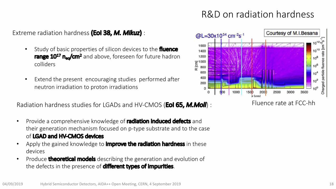
R&D on radiation hardness
Extreme radiation hardness (EoI 38, M. Mikuz) :
• Study of basic properties of silicon devices to the fluence range 1017 neq/cm2 and above, foreseen for future hadron colliders
• Extend the present encouraging studies performed after neutron irradiation to proton irradiations
Radiation hardness studies for LGADs and HV-CMOS (EoI 65, M.Moll) :
• Provide a comprehensive knowledge of radiation induced defects and their generation mechanism focused on p-type substrate and to the case of LGAD and HV-CMOS devices
• Apply the gained knowledge to improve the radiation hardness in these devices
• Produce theoretical models describing the generation and evolution of the defects in the presence of different types of impurities.
Fluence rate at FCC-hh
04/09/2019 Hybrid Semiconductor Detectors, AIDA++ Open Meeting, CERN, 4 September 2019

19
Tools for investigation of silicon devices
Two Photon Absorption TCT (EoI 66, M. Moll) :
TPA-TCT creates charges only in a tiny voxel in the focal point of the laser beam à true three dimensional TCT characterization possible• Complete the development from the proof-of-concept
installation towards a user-friendly TCT system to offer a sensor characterization service to the full community
“RadHardSi” Systematic studies of radiation damage in silicon sensors (EoI 159, O. Brandt) :
• Studies of radiation damage up to the fluences foreseen at FCC-hh with high statistics systematic studies of process variations àautomated test set-up tailored to carry out standardized measurements on dedicated new test-structures in a controlled environment
• Target of improving the radiation hardness of commercially (??) produced silicon detectors
04/09/2019 Hybrid Semiconductor Detectors, AIDA++ Open Meeting, CERN, 4 September 2019

20
Other semiconductor materialsDevelopment of 3D diamond detectors (EoI 108, A. Oh) :
Femto-second laser micro-machining techniques to form electrically conductive nano-graphite wires à
optimise the design and properties of 3D diamond devices for applications that require high radiation tolerance and excellent timing resolution
3D SiC detectors for harsh environment (EoI 4, G. Pellegrini) :
Optimize 3D sensor processing through a doping-selective electrochemical-etching method able tocreate deep holes in SiC.
• Renewed interest due to progress in wafer fabrication (high quality material in 6” wafers)
• Fabrication and full characterisation of 3D SiC detectors as small chips
3D detectors based on a-Si:H for particle tracking(EoI 94, M. Menichelli) :
• Moderate leakage current levels also after irradiation
• Use 3D detectors to overcome high depletion voltages
04/09/2019 Hybrid Semiconductor Detectors, AIDA++ Open Meeting, CERN, 4 September 2019

21
Conclusions
04/09/2019
• 24 different proposals in the field of hybrid semiconductor detectors• 37 institutes and 4 companies• ~4 M Euro EU funds requested in total
• Very diversified proposals in terms of technologies and scope, with a substantial shift of interests with respect to the detectors currently employed or in constructions for the running experiments:• mainly timing + extreme radiation hardness
• Several EoIs have large overlaps and could be merged for the final proposal towards common deliverables
Very strong interest of the HEP community in this detector field!
Hybrid Semiconductor Detectors, AIDA++ Open Meeting, CERN, 4 September 2019