Embed Size (px)
Citation preview

Bergische Universität Wuppertal
Fachbereich Elektrotechnik, Informationstechnik, Medientechnik
Hybrid organic-inorganic structures for
solution processed organic light emitting diodes (OLEDs)
zur Erlangung des akademischen Grades eines
Dr.-Ing.
genehmigte Dissertation
von
Author : Danny Krautz, Dipl.-Ing., M. Sc.
Referent : Prof. Dr. rer. nat. Thomas Riedl
Korreferent : Prof. Dr. rer. nat. Ullrich Scherf
Tag der mündlichen Prüfung : 11.04.2014

Die Dissertation kann wie folgt zitiert werden: urn:nbn:de:hbz:468-20140625-113409-8[http://nbn-resolving.de/urn/resolver.pl?urn=urn%3Anbn%3Ade%3Ahbz%3A468-20140625-113409-8]

Contents
1 Introduction and Motivation 7
2 Fundamentals and experimental details of organic light emitting diodes (OLEDs) 11
2.1 Theoretical background of organic light emitting diodes . . . . . . . . . . . . . . 11
2.1.1 Fundamentals of organic semiconductors . . . . . . . . . . .. . . . . . 12
2.1.2 Charge injection and transport processes . . . . . . . . . . .. . . . . . . 18
2.1.3 Optical losses within the OLED structure . . . . . . . . . . .. . . . . . 22
2.2 Deposition techniques and processing procedure of OLEDdevices . . . . . . . . 26
2.2.1 Atomic layer deposition . . . . . . . . . . . . . . . . . . . . . . . . .. 27
2.2.2 Measurement techniques . . . . . . . . . . . . . . . . . . . . . . . . .. 29
3 Ultra Thin Metal electrode for OLEDs 33
3.1 Experimental details . . . . . . . . . . . . . . . . . . . . . . . . . . . . .. . . 34
3.2 Characterization of the ultra thin metal electrodes . . . .. . . . . . . . . . . . . 36
3.3 Nickel UTMF as bottom anode for OLEDs . . . . . . . . . . . . . . . . .. . . 39
3.3.1 Influence of the Ni layer thickness on the performance of OLEDs . . . . 40
3.3.2 Increased efficiency of Ni-OLEDs due to improved electron injection . . 48
3.3.3 Influence of the oxidation of the UTMF on device performance . . . . . 54
3.4 Further improvements of UTMF layer using double metal layer . . . . . . . . . . 59
3.4.1 Properties of Ni, Cu and CuNi as UTMF . . . . . . . . . . . . . . . . . 59
3.4.2 Double metal layer as anode for bottom light emitting diodes . . . . . . . 64
3.5 Conclusions . . . . . . . . . . . . . . . . . . . . . . . . . . . . . . . . . . . . . 71
4 Atomic Layer Deposition (ALD) Technique applied to multilayer organic LEDs 74
4.1 Experimental details . . . . . . . . . . . . . . . . . . . . . . . . . . . . .. . . 75
i

Contents ii
4.2 Effect of the deposition process on the intrinsic properties of organics . . . . . . 76
4.3 The ALD layer used to avoid intermixing of successive spin coated organic layers 85
4.3.1 Study of the solvent influence on the underlying layer.. . . . . . . . . . 86
4.3.2 Application to multilayer OLEDs; avoidance of intermixing of the layers 88
4.4 Conclusion . . . . . . . . . . . . . . . . . . . . . . . . . . . . . . . . . . . . . 98
5 Blend of a polymer and an organic small molecule as emissive layer for OLEDs 100
5.1 Experimental details . . . . . . . . . . . . . . . . . . . . . . . . . . . . .. . . 101
5.2 Spectroscopy Study of the Energy transfer mechanism . . .. . . . . . . . . . . 102
5.3 Performance of the blend as emissive layer for OLEDs . . . .. . . . . . . . . . 109
5.4 Conclusion . . . . . . . . . . . . . . . . . . . . . . . . . . . . . . . . . . . . . 119
6 Summary and Outlook 120
List of figures 129
A Figures 131
List of tables 131
B Tables 137
C Transfer Matrix Formalism 139
Bibliography 142
D Publications 152

Hiermit versichere ich, die vorliegende Arbeit selbstständig verfasst und nur die angegebenen
Quellen und Hilfsmittel verwendet zu haben.
Hiermit versichere ich, dass die Dissertation in der vorgelegten oder einer ähnlichen Fassung
noch nicht zu einem früheren Zeitpunkt an der Bergische Universität Wuppertal oder einer an-
deren in – oder ausländischen Hochschule als Dissertation eingereicht worden ist.
Danny Krautz
1

Thanks
It has been a pleasure to work at the Fraunhofer IAP and to have the guidance of Prof. Dr.
Thomas Riedl from the University Wuppertal as my supervisorfor the past three years. This
time has been a memorable and valuable experience. This thesis would never have seen the light
of day without my supervisor’s inspiration and superb guidance. Therefore, I would like to say
thank you to Prof. Dr. Thomas Riedl who has been always approachable, patient, supportive and
enthusiastic.
I also would like to thank Prof. Dr. Ullrich Scherf for being myco-adviser and for his valuable
support.
Dr. Armin Wedel from the Fraunhofer IAP has always given soundadvice that have lead to better
ways of continuing my studies and I appreciate his support regarding my thesis and my work at
the Fraunhofer IAP.
I am very grateful to the MERCK Southampton team for the exceptional experience during my
research stay and in particular to Dr. Michael Heckmeier, Dr. Frank Meyer, Dr. David Sparrowe
and Dr. Miguel Carrasco.
A thesis would not be possible with supportive and helpful colleagues. I appreciated the time
spent with them inside the lab and in the real world. I enjoyed the time riding the bike to the ICFO
with Dr. Lars Neumann, I enjoyed the first months sharing the cleanroom with Dr. Dominico Tulli
and I enjoyed our little German island with Dr. Sybille Braungardt and Dr. Florian Wolfgramm.
Additionally, I am grateful to Manuela Furkert and Luis Enrique who helped me with the lab
equipment and administrative work at ICFO.
The Fraunhofer IAP group is too large to thank everyone individually, but members from the past
and from the present have made it a brilliant environment to work in. In special, I would like to
2

Contents 3
say thanks to my colleagues from the Fraunhofer Institute. In particular, Dr. Tonino Greco for
all the valueable discussions and for giving me motivation during the writing of the dissertation;
Dr. Alexander Lange for the help of the AFM measurements; Stefanie Kreißl for processing of
the samples; and Dr. Christine Boeffel for all the fruitful discussions.
I would like to thank Dr. Steve Albrecht for introducing me to the facilities from the soft matter
group at the University of Potsdam.
The thesis is coming to an end and I hope my friends will be able to breathe again. They helped
me so much that I cannot express in words how much I appreciate their friendship and endless
support. Markus, Maik, Silvio, Lu, Francesca, Sabrina, Martin, Korbi, Jimmy, Fred, Kathrin,
Maria and Ronny, you all together are part of this story.
My mother has always been my biggest fan and gave me the biggestsupport through good and
hard times. Love to you always.
Milene, thanks for having been a brilliant support during myPhD, I would not have gone this
far without you. Thank you for trusting my capabilities during the PhD period and for being the
best what happened to me. You gave me the biggest present in life, Luisa. Thank you. I love you!

List of Abbreviations
General
ALD Atomic layer deposition
LCD Liquid Crystal Display
OLED Organic Light Emitting Diode
HOMO Highest Occupied Molecular Orbital
LUMO Lowest Unoccupied Molecular Orbital
ITO Indium Tin Oxide
HTL Hole Transport Layer
HBL Hole Blocking Layer
ETL Electron Transport Layer
EBL Electron blocking Layer
PL Photoluminescence
EL Electroluminescence
AFM Atomic Force Microscope
RPM Revolutions Per Minute
FN Fowler-Nordheim tunneling
RS Richardson-Schottky thermionic emission
SCLC Space-Charge-Limited-Current
PLQE Photoluminescence quantum Efficiency
PLED Polymer light emitting diode
4

Contents 5
Symbol Unit Description
U V Voltage
I A Current
F V/m Electric Field
J A/m2 Current Density
L cd/m2 Luminance
Ro nm Intermolecular Distance
µn,p cm2/Vs Charge Carrier Mobility
µ0 cm2/Vs Low-Field Mobility
ηext % external efficiency
ηr % internal efficiency
ηout % outcoupling efficiency
ηmol % photoluminescence efficiency
γ % charge-carrier balance
EB eV Potential Barrier between LUMO and metal
Np,n eV−1 Density of States
UTFL V Trap Filling Voltage
ε0 / Dielectric Constant
Θ / Trapping Factor
N,PT cm−3 Number of Trap States
kB eV/K Boltzmann Constant
q C Electrical Charge on the Electron
n / Refrective Index
τ s Natural Radiative Lifetime
τr s Overall Lifetime

Contents 6
Materials
Alq3 tris-(8-hydroxyquinoline) Aluminum
PEDOT-PSS polyethylenedioxythiophene:polystyrenesulfonate
PFO Poly(9,9-dioctylfluorene)
SY Poly(phenylenevinylene) co-polymer
MEH-PPV poly[2-methoxy-5-(28-ethyl-hexyloxy)-1,4-phenyl-enevinylene]
Al Aluminium
Al2O3 Aluminum Oxide
ITO Indium-Tin-Oxide
Ni Nickel
Ti Titanium
Cu Copper
Ag Silver
Au Gold
N2 Nitrogen
CHCl3 Chloroform
Tol Toluene
THF Tetrahydrofuran
CB Chlorobenzene
H2O Water

Chapter 1
Introduction and Motivation
More than 20 years ago, in 1987, Tang and V. Slyke reported thefirst efficient small molecule
(SM)-based light emitting device using tris(8-hydroxyquinoline) aluminum Alq3 as active layer
[1]. Three years later, a breakthrough for polymer light emitting diodes (PLEDs) was reached
through the discovery of electroluminescence from poly(para-phenylene vinylene) polymers at
the University of Cambridge [2]. Since then, developments ofvarious polymer or small molecule
materials [3][4] and a range of OLED architectures [5] have been investigated [6][7]. Just a
few years after the above mentioned discoveries, the growinginterest in industry and research
opened a new market for the so-called organic electronics and, in recent times, this technology
has shown its true potential for overcoming some of the limitations of inorganic semiconductor
devices [8].
Organic devices based on small molecules are already placedon the market. [9][10]. In 2002,
Philips and Pioneer supplied OLEDs already in a commercial scale for mobile display applica-
tions. Only one year later, Kodak introduced the first AMOLEDdigital camera - the KODAK
EasyShare LS633. Samsung’s OLED production based on small molecules reached mass pro-
duction in 2008 and this is basically due to the use of the OLEDdisplays in their mobile phone
applications. For displays, organics offer many advantages compared to the current technology
of LCD and Plasma screens [11][12]. Apart from economic advantages and the requirement of
simpler fabrication steps and technology, they also offer lower power consumption [13], a wider
viewing angle[5] and faster response time [14]. However, there are still many challenges until
OLEDs can be integrated in our daily life. Environmental conditions, such as high temperature
7

1. Introduction and Motivation 8
and high humidity, lower the operating lifetime due to the degradation of the organic material
and the use of highly reactive electrode materials. Research work nowadays focuses on the in-
crease of the device lifetime avoiding electrode materialslike calcium or barium and improving
the encapsulation. In addition, there is an ever growing impetus to avoid the use of less abundant
and costly materials.
In this thesis, novel metal combinations, such as ultrathinmetal bilayer, are studied to replace
ITO, which is still a bottleneck for the introduction of organic devices into the mass market due to
its high cost and high process temperature, which is not compatible for the deposition on flexible
substrates such as PET. ITO is a high cost material composition based on rare indium(III) oxide
(In2O3) and tin(IV) oxide (SnO2). Another disadvantage of ITO, looking at the device structure,
is that most of the light is trapped inside the device due to the need of a relatively thick ITO layer
as transparent bottom electrode. Various approaches for animproved light outcoupling have
been proposed and successfully applied into the OLED structure [15]-[18]. Indeed, most of the
presented solutions still use ITO as anode material with either a modified surface or capped with
an additional metal layer. The study in chapter 3 addresses some of the approaches in this area,
such as OLED manufacturing with low cost alternative semitransparent and highly conductive
substrates [19]. Nickel (Ni) is widely studied as an ultra-thinlayer in terms of transmittance,
conductivity and morphology and then Ni is applied as anode material for OLEDs. Ni-OLEDs
show reasonable efficiencies at a comparable brightness, inrespect to the ITO reference device.
It is demonstrated that pure Ni is very stable against temperature and humidity. Better electrical
and optical properties can be measured for pure copper (Cu), however, it shows poor stability
during environmental tests (humidity and temperature). Anexcellent trade-off between the Ni-
stability and the optical and electrical properties of Cu is found by forming a double-layer based
on Cu and Ni. The bilayered CuNi ultra-thin metal films (UTMF) showexcellent stability against
temperature and oxidation. When applied to OLEDs, the devices show high efficiency, almost as
good as ITO-based devices with good operation stability overtime. Thus, it is shown that Ni and
NiCu are potentially better candidates as semitransparent anode material for OLED applications
due to easy fabrication, use of low cost material, low material consumption and a reasonable
OLED efficiency.
A growing research and industry interest on solution processed OLEDs can be noticed despite
the fact that the performance has not reached the one of vacuum deposited devices. However,
solution processed OLEDs can be fabricated via different printing techniques. In the future,

1. Introduction and Motivation 9
it might be even possible to use roll-to-roll (R2R) processes on a continuous web, similarly to
the printing process of newspapers. Such R2R-process tools include usually a Slot Die and/or
Inkjet print-system for the deposition of the electrodes and the active material. The R2R process
would decrease significantly the cost of the OLED fabrication, which could make OLED a seri-
ous competitor of lighting and display technologies. Smallmolecules became printable and the
replacement of the commonly vacuum deposited electrodes with printable materials encourages
the industrialization of solution processed OLEDs. A particular challenge of solution processed
OLEDs is the preparation of multilayer devices. A concept for the preparation of solution pro-
cessed multilayer devices is presented. The insertion of thin A2O3 layer prepared by atomic layer
deposition protects the organic layer on the substrate against the solvent used in the deposition
of the subsequent layer. [22]. Specifically, within this study, Alq3 as electron-transport material
is spin-coated onto an Al2O3 protected emissive polymer layer. The brightness of the device is
furthermore significantly enhanced due to the presence of the electron transport layer and the
avoided dissolution of the emissive polymer. This study proves successful the concept behind this
idea and a further enhancement of the OLED efficiency can be very likely achieved by choosing
a different material combination. However, such a process shows again the importance of the
ALD-process integration into a R2R process due to its extended range of processing possibilities.
The application of the ALD is therefore not only limited to the encapsulation process when used
for organic electronics.
Avoiding the intermixing of materials for solution processed multilayer structures is one of the
main approaches in chapter 4. However, a careful intermixingof two or more polymer materials
might lead also to an increase of the host polymer performance when choosing a proper guest-
host relation. Usually an emissive hole-conductive host polymer is blended with a non-emissive
electron conductive guest polymer [20]. In chapter 5, a different approach is presented based
on an emissive polymer as host material doped with an emissivesmall molecule. MEH-PPV
and Alq3, both emissive materials and commercially available, are blended successfully together
without changing the emission spectra of MEH-PPV as host material. The energy transfer of
MEH-PPV doped with Alq3 varying the concentration is investigated in this chapter and such a
blend is successfully applied as emissive layer into an OLEDstructure. Both concepts, the use of
multilayer structures (chapter 4), and the blending of the host material are compared. The same
emitter, MEH-PPV, is used and Alq3 is either spin-coated or used as dopand. Both concepts
show a significant increase of the OLED efficiency compared tothe MEH-PPV reference OLED.

1. Introduction and Motivation 10
The blended OLED shows still a higher efficiency and lower required voltage for the maximum
light emission. Blending of the host with a charge carrier emitter shows a significant advantage
compared to multilayer structure, due to lower process cost,since less process steps are needed.
Furthermore, a multilayer device fabrication requires additional process steps (for instance,
cross-linking or protection layer) to avoid intermixing ofthe solution processed layers.

Chapter 2
Fundamentals and experimental details of
organic light emitting diodes (OLEDs)
Understanding the physics and process requirements of semiconducting polymers are crucial for
the successful implementation of the polymer as emissive layer in (OLEDs). The fundamentals
of conductive polymers as well as their optical and electrical characteristics are explained in the
following chapter. The fabrication techniques used in this thesis are described and the process
recipes are listed.
2.1 Theoretical background of organic light emitting diodes
Semiconducting conjugated polymers have attracted much interest recently. These materials
combine the processability and outstanding mechanical characteristics of polymers with the
ready-tailored electrical and optical properties of functional organic molecules. The electronic
characteristics of these materials are primarily governedby the nature of the molecular structure,
but intermolecular interactions also exert a significant influence on the macroscopic material
properties. Polymer light emitting diodes consist of a stack of layers where an electrically ex-
cited fluorescent polymer is sandwiched between two conductive electrodes. At least one of
the electrodes has to be transparent for the outcoming light; this can be either the anode or the
cathode depending on the OLED configuration (standard or inverted). A simple OLED stack is
shown in figure 2.1a with an emissive polymer sandwiched between two electrodes. A photo-
11

2. Fundamentals and experimental details of organic light emitting diodes (OLEDs) 12
graph has been taken and is shown in figure 2.1b from a fabricated working device. This device is
the so-called bottom-light emitting diode configuration, meaning that the top-electrode (cathode)
is opaque, so that the emission of light takes place through the glass substrate.
(a) (b)
Figure 2.1: a simple OLED stack (a) can be electrically excited for light emission (b)
A successful electrical excitation requires the injectionof charges, the transport through the
layers as well as a balanced amount of positive and negative charges within the active emissive
material resulting in an effective formation of excitions for the radiative recombination. The
following subchapters give an insight of some of the fundamental processes within the OLED
structure.
2.1.1 Fundamentals of organic semiconductors
When two atoms interact to form a molecule, they form a chemical bond either by creating a
bonding molecular orbital or an antibonding molecular orbital. A bonding molecular orbital is
formed when the wavefunction of the two reacting electrons is in phase; an antibonding molec-
ular orbital will be created when the wavefunction is 180 displaced forming a nodal point (am-
plitude = 0). Orbitals that lie along the bond axis are calledσ-bonds and are very strong and
highly localized in space. They do not allow mobile charge carriers and are largely responsible
for the shape and the structure of the molecule. Theπ-bonds lie above and below the plane of the

2. Fundamentals and experimental details of organic light emitting diodes (OLEDs) 13
polymer backbone, are spatially delocalized over the entire conjugated segment, and are much
weaker [21]. Electrons in theπ orbital make this particular class of organic materials conduc-
tive. A π-bond and aσ-bond can form a double bond resulting in the formation of a combined
orbital, the so-called molecular orbital. Normally, the highest occupied and lowest unoccupied
molecular orbitals (HOMO and LUMO, respectively) in organic semiconductor molecules areπorbitals. The energy difference between the HOMO and the LUMO is then regarded as band gap
energy with a typical energy between 1.5 eV - 3 eV [22][22], asschematically shown in figure
2.2. Therefore, the HOMO corresponds to bondingπ and LUMO to anti-bondingπ∗ orbitals
which have higher energy. In a simplified analogy, the HOMO and LUMO levels are to organic
semiconductors what valence and conduction bands are to inorganic semiconductors. By adding
more conjugated double bonds into the system, more molecular orbitals will be created leading
to a decrease of the energy gap between the highest occupied molecular orbital (HOMO) and the
lowest unoccupied molecular orbital (LUMO). As a result, light with a longer wavelength will
be absorbed.
(a) (b)
Figure 2.2: molecular orbital of Ethylene (a) and the corresponding band splitting (b)
A consideration of the HOMO and LUMO level is mandatory for a well-balanced injection of
positive and negative charges when using conjugated polymers in OLED devices. The electrodes
(anode and cathode) are usually defined by the workfunction which should be aligned to the
HOMO and LUMO level. Assuming a proper injection and transport of the charges towards the
polymer center, an exciton (a bounded state of an electron and a hole) will be formed creating an
excited state. Indeed, two processes are in charge of the formation of an exciton. The first process

2. Fundamentals and experimental details of organic light emitting diodes (OLEDs) 14
is also known as Langevin recombination where an exciton is formed due to the recombination
of an electron-hole pair. This recombination mechanism is dependent on the injection and the
transport of the charges and is more efficient for a well-balanced number of positive and negative
charges. The second process is related to the photon absorption via optical excitation where
an electron of the ground state will be excited towards the HOMO molecular orbital. For both
processes, the excited molecule keeps this gained energy for a very short time, approximately
10−9 to 10−7s until it falls back to the ground level by releasing its energy.
The Jablonski-diagram (figure 2.3) illustrates the electronic states of a molecule and the transi-
tions between them. The singlet ground state S0 and the excited singlet states Sn+1 with n > 1
as well as the triplet states T1 and T2 are shown in the diagram. The ground state can only be a
singlet state regarding Paulis exclusion principle. Therefore, only the singlet state can be excited
via photoabsorption. The excitation of an electron from theground state S0 by photoabsorption
generates an excited state in Sn+1 with n > 1 [24]. The radiative recombination from Sn to S0 is
known as fluorescence. A radiative decay from the triplet state to the ground state is spin for-
bidden. Such a radiative decay is called phosphorescence and has a much smaller recombination
rate than for the fluorescence [22][29].
However, the emission probability for each molecule is time-independent and the emission inten-
sity depends in fact only on the number of molecules in the excited state. The ideal exponential
decay of the fluorescence intensity of the excited molecule can be described with the following
law:
I = I0e−k0 t (2.1)
I0 and I describe the intensity of the emitted radiation directly after the excitation and after
passing the time t.k0 is known as velocity constant and can be calculated from the average
lifetime of the excited state (equation 2.2).
k0 =1τ0
(2.2)
The lifetimeτ0 is almost temperature independent, but it depends on environmental conditions
and also the used solvents. The estimated value for the rate constant for the fluorescence is be-
tweenkF =106 -109s−1. The phosphorescence process is forbidden by nature so thatthe velocity

2. Fundamentals and experimental details of organic light emitting diodes (OLEDs) 15
constant withkP=10−2 -104s−1 is much smaller than for the fluorescence [26].
Sn
S1
Phosphorescence
Ground StateSo
Excited Singlet State
IC
S2Excited Triplet State
IC
T1
Tn
T2
FluorescenceAbsorption
ISC
Figure 2.3: energy transfers and recombination mechanism explained by the Jablonski diagram
The electrical excitation is different from the photoexcitation and involves basically the charge
transfer and the diffusion of the electrons and holes in the polymer material until they are at-
tracted by their mutual coulomb force and recombine either to form a singlet or a triplet state.
The 3:1 law occurs in that case where many more triplet statesare formed and the intersystem
crossing from singlet to triplet can still happen. The internal conversion (IC) is the transfer with
the same spin-multiplicity. Such a non-radiative transition occurs between higher excited states
Sn+1 to S1. On the other hand, electron transfer between states of different multiplicities via
spin-inversion is called intersystem crossing, which is basically the conversion from the triplet
state to the singlet state or vice versa [25]. Only 25 % of all excitons created in this described
way are singlets and 75 % are triplets according to the quantum mechanical rules (also known
as 3:1 rule) which limits the internal quantum efficiency of OLEDs. The limitation of the in-
ternal quantum efficiency is due to the low probability of a radiative recombination of triplet
excitions. Therefore, only the radiative recombination ofsinglet excitons contributes to the emit-
ted light [21]. The electroluminescence efficiency is normally lower than the photoluminescence
efficiency since not all the injected holes and electrons recombine to form excitons and only a
fraction of these are in the singlet state [27].
The presence of molecules from different species might leadto either a fluorescence enhance-
ment or a fluorescence quenching due to the possible energy transfer between the molecules. The
presence of a donor molecule might result in a change of the polymer chain aggregation of the

2. Fundamentals and experimental details of organic light emitting diodes (OLEDs) 16
host polymer. It has been described that MEH-PPV chains are expected to coil more tightly in
CHCl3. The figure 2.4 just illustrates the possible influence of theAlq3 dopand on the MEH-
PPV aggregation. The size of the MEH-PPV (hydrodynamic radius) has been reported to be
between 10 and 30 nm depending on the solvent and on the molecular weight, whereas the size
of the small molecule Alq3 is around 2 nm. The energy transfer between the acceptor (in the
presented case MEH-PPV) and the donor (in this example, Alq3) becomes more dominant for
a high donor concentration compared to the energy transfer between polymer chains from the
same species. Such an energy transfer might lead to a significant emission enhancement when
the molecules (donor and acceptor) are properly chosen. A schematic example for the donor and
acceptor behavior is shown in the following figure:
(a) MEH-PPV polymer chains (b) MEH-PPV doped with Alq3
Figure 2.4: MEH-PPV polymer chain with schematically showninterchain energy transfer (a), MEH-PPV doped
with Alq3 and the corresponding energy transfer between the polymer chain and the molecules.
The energy transfer of the excitons in figure 2.4 is indicatedas red arrows. Excitons can transfer
energy from an excited donor species D∗ to an acceptor species A. In that case, a non-radiative
energy transfer may occur, the so-called Förster transfer or the Dexter transfer [28][29]. The
principle is schematically shown in figure 2.5.
An explanation for the energy transfer by the Dexter processcan be found for a very short dis-
tance in the order of 10 Å or below with a significant overlap ofthe molecular orbitals. The
Dexter process is based on the electron exchange between thedonor and the acceptor with a de-
creased energy transfer probability for larger distances between them. A strong overlap between
the absorption and emission spectrum of the donor and acceptor is not required, however, the
exciton energy of the acceptor should be lower than that of the donor molecule for an efficient
transfer [26]. The Dexter transfer allows both singlet-singlet and triplet-triplet transitions [30].

2. Fundamentals and experimental details of organic light emitting diodes (OLEDs) 17
Singlet Exciton
Triplet Exciton
ISC
Förster Transfer
Dexter Transfer
DonorAcceptorSo
Figure 2.5: schematic of an Förster (long range) and Dexter (short range) transfer
The Förster process explains the energy transfer for an intermolecular distance lower than 100
Å. The excited electrons (donor molecule) act as an oscillating dipole resulting in an alternating
electric field which again creates an oscillating dipole in the acceptor molecule. Only singlet-
singlet energy transfer is created by the Förster process since the spin state of the donor and
acceptor is the same. An example of a strong overlap between the emission spectrum of the
donor and the absorption spectrum of the host polymer have been shown in figure 2.6 with an
overlap between 450 nm and 575 nm of absorption spectrum of MEH-PPV and the emission
spectrum from Alq3.
350 400 450 500 550 600 650 700 7500.0
0.2
0.4
0.6
0.8
1.0 Extinction MEH-PPV
norm
. ext
inct
ion
(a.u
.)
Wavelength (nm)
0.0
0.2
0.4
0.6
0.8
1.0 Photoluminescence Alq3
norm. photolum
inescence intensity (a.u.)
Figure 2.6: absorption spectrum for MEH-PPV and photoluminescence spectrum for Alq3, strong overlap between
450 nm and 575 nm.
If one monomer is in an excited state, the intermolecular interaction is described as excimer. The

2. Fundamentals and experimental details of organic light emitting diodes (OLEDs) 18
term excimer refers to the interaction of equal monomers in which one is originally in the excited
state and the other is in the ground state. The excited state interaction of different monomers is
known as exciplex. Bimolecular excited states can be formed via electron-transfer from donor
to acceptor using blends consisting of at least two components. In that case, exciplexes can have
either singlet or triplet character dependent on the acceptor. An exciplex is therefore similar to
an exciton with electrons and holes on different molecules.
Excimer and exciplex emission is typically broad and unstructured and shifted to lower energies
with respect to the emission of the monomer. Both charge-carriers are able to form either ex-
cimer or molecular emissive states when injecting holes andelectrons via electrical excitation.
Therefore the PL and EL spectrum might differ due to the various types of excimer (singlet and
triplet) which can be formed via electrical excitation [31]. Note that excimer and exciplex can be
observed in both, the PL and the EL spectrum [30][32].
2.1.2 Charge injection and transport processes
The current-voltage characteristic for organic light emitting diodes is characterized mainly by
two effects, the injection of the charge carriers from the electrodes into the devices and the
charge carrier transport within the device structure limited by the organic material properties.
This subsection gives an overview of the commonly applied injection processes of OLEDs and
the current voltage behavior defined by its characteristic regions.
Charge carrier injection mechanism
The OLED device performance is strongly related to a balanceinjection of negative (electrons)
and positive (holes) charges. When applying a voltage, negative and positive charges have to
overcome the energy barrier between the electrodes and the organic material. This energy barrier
is the result of the difference of the metal workfunction andthe HOMO or LUMO level of the
polymer. Two main processes are involved in the injection ofcharges, the Fowler-Nordheim
tunneling (FN) and Richardson-Schottky (RS) thermionic emission (figure 2.7).

2. Fundamentals and experimental details of organic light emitting diodes (OLEDs) 19
Figure 2.7: metal-semiconductor contact without an applied electric field (a), Richardson-Schottky (RS) and Fowler-
Nordheim (FN) injection mechanisms after applying a voltage V with the electric field E (b)
The first model, the FN tunneling mechanism, describes the tunneling principle of charges from
the metal electrode through a triangular barrier into the polymer material, independent of the
temperature [33]. The triangular potential barrier results from the applied electrical field and the
tilt of the energy levels of the semiconductor. The slope of the tilt depends on the electric field
strength and thus the barrier width becomes field dependent.In equation 2.3 it can be seen that
the injection current is limited by the potential barrier EB between the electrode and the polymer
material and the electric field E [34][35].
JFN =2,2(qE)2
8πhEBexp
−8π√
2qm∗E32B
3hE
(2.3)
The second mechanism for the injection of charges is known asthe Richardson-Schottky (RS)
thermionic emission [36][37]. Three effects are importantfor this model [38]. The first effect is
the potential difference EB between the workfunction of the electrode metal and the LUMOen-
ergy level for the electrons of the polymer material. For thesecond effect, the applied electrical
field manipulates the characteristics of the potential, which results in the typical triangular poten-
tial barrier. The last effect results from the image potential of the injected charges. The magnitude
of the electrostatic force EL between two point charges can be calculated by coulombs law and is
inversely proportional to the square of the distance between the charges. The total potential as a

2. Fundamentals and experimental details of organic light emitting diodes (OLEDs) 20
function of the distance is the result of the superposition of those three potentials. The potential
difference EB will be therefore lowered due to the resulting electrical field of the image force.
This lowering of the potential is the so-called Schottky-effect. We obtain the total current as the
final result. As described by equation 2.4, the current depends on the temperature, the applied
electrical field and the lowering of the potential barrier atthe electrode-polymer interface through
the image force [39].
Jth =4πqm∗ (T kB)
2
h3 exp
(
Eb1 − EB
kBT
)
(2.4)
To summarize, several effects increase the injection of thecharge carrier into the OLED when
looking at equations 2.3 and 2.4. Increasing the applied electric field increases also the injection
of charges due to the lowered potential difference. However, a low applied electric field (low
turn-on voltage) is required for commercial OLED application. A key element for tuning the
charge carrier injection is lowering the potential difference EB by aligning the workfunction of
the cathode to HOMO energy level of the Polymer for an increased injection of the holes and
also aligning the workfunction of the cathode to the LUMO level of the polymer for an increased
injection of electrons.
Space-charge-limited current (SCLC) model
The current-voltage behavior curve of the OLEDs can be described with the space-charge-
limited-currents (SCLC) model. The SCLC model includes the material properties, the charge-
carrier-mobility and also the intrinsic charge-carrier concentration of the polymer semiconduc-
tors [40]. Four regions can be distinguished in the I-V curveas it is schematically shown in figure
2.8:

2. Fundamentals and experimental details of organic light emitting diodes (OLEDs) 21
Figure 2.8: current-voltage behavior with traps, ohmic andSCLC transition, with n > i
A perfect single layer device with two symmetric, ohmic contacts, free of traps and a free charge
carrier mobility has been assumed. The diffusion current aswell as the charge carrier densities
at the thermal equilibrium has been neglected in this assumption. The thermally generated free
holes override the square law at low electric field where the number of injected holes is quite
low. This so-called ohmic region occurs until the average density of injected excess free charges
becomes comparable with the thermally generated one. The description of the ohmic region can
be found in equation 2.5 [41]:
J = qn0µUd
(2.5)
The current density is proportional to the applied voltage and to the thermionic intrinsic charge
carrier density n0. When the applied voltage is high enough, more charge carriers are injected
than are present during the transport process within the polymer layer. Taking x = d and V = V(d)
and taking into account the boundary condition (E(x = 0) = 0),we obtain the current voltage char-
acteristic, also known as the trap-free square law, the Mott-Gurnay square law as described in

2. Fundamentals and experimental details of organic light emitting diodes (OLEDs) 22
equation 2.6 [35][36]:
J =98
εε0µU2
d3 (2.6)
A perfect organic single layer device is not a realistic object, but the equation 2.6 can be used
when the applied voltage is high enough. At high voltages, the total number of injected holes
is substantially higher than the total number of empty trapsin the material. The number of free
charges will be reduced at lower injection levels by the presence of charge traps, which can
be impurities or structural defects. Those empty traps willcapture a number of free charges
and therefore the current through the device will be limited. The characteristic range of voltage
where the current abruptly increases is called the trap-filled limit, and UTFL is the characteristic
voltage to reach trap filling. The position of this crossoverfor discrete levels of traps is roughly
estimated from the formula in equation 2.7 [41]:
UTFL =q pT d2
2ε(2.7)
As the current flow grows with applied bias, the quasi-Fermi level moves closer to the valence
band and may eventually cross the energy level of the trap. Atthis point, the traps will become
essentially filled and further injected free carriers will,therefore, not be trapped.
2.1.3 Optical losses within the OLED structure
Optimizing the light extraction of OLEDs is a particular interest in research nowadays. The
external efficiencyηext is related to the internal quantum efficiencyηint of the organic material
and the out-coupling efficiencyηout of the multilayer planar structure as shown in equation 2.8:
ηext = ηint ηout (2.8)
It has been shown that 40 - 50 % of the generated light of the light emissive polymer is trapped
within the ITO-layer and/or absorbed as surface plasmon on the metal-polymer interface [42].
Part of the light (20 - 30 %) is totally reflected on the interface between the substrate and air and
will be therefore guided to the lateral faces of the device. This part of the light is basically not
2. Fundamentals and experimental details of organic light emitting diodes (OLEDs) 23
lost since it can be directed orthogonal to the surface usingoptical systems [43]. A maximum
external efficiency of around 20 - 30 % can be therefore achieved [44].
An OLED stack consists of different organic and inorganic layers with their specific optical prop-
erties. The transmission, absorption, reflection as well asthe optical coefficient n and extinction
coefficient k of these materials are wavelength dependent. Acommon methodology for optimiz-
ing the OLED stack in respect to the emission wavelength of the polymer can be found using the
transfer-matrix analysis (appendix C). The optical properties of the OLED stack will be therefore
described as a matrix where the wavelength dependence of theoptical parameters is considered.
The characteristics of the optical properties of each material are given by the complex refractive
index which can be described with the following formula:
N(λ) = n(λ) − ik(λ) (2.9)
The complex refractive index is wavelength dependent and can be either measured for a known
layer thickness using the spectroscopic ellipsometry or calculated from the optical properties. A
simplified method for the calculation of the complex refractive index n of a thin film with a low
absorption has been already described in 1975 by J. C. Manifacie et.al.[52]. In this thesis, the
refractive index and the absorption coefficient have been calculated from the transmission and
reflection measurements. The imaginary part of the index of refraction is related to the absorption
coefficientα and the wavelength of lightλ, shown in equation 2.10:
k =λα4π
(2.10)
The absorption coefficient can be determined by the optical transmission measurement and the
thickness of the measured film. This parameter is also known as optical density (OD) with the
following relationship:
α =ODln(10)
x(2.11)
The incoming light intensity is given by I in equation 2.12:
IIo
= e−αx (2.12)

2. Fundamentals and experimental details of organic light emitting diodes (OLEDs) 24
The remained light intensity after passing through a film with a thickness x is named with Io .
Basically, the transmission decay through an absorbing medium has been described in equation
2.12. Using these equations and the Matrix Transfer formulation, the refractive index n and the
absorption coefficient k can be calculated over the wavelength and with these results, the out-
coupling efficiency can be evaluated under the consideration of losses due to the formation of
optical modes within the dielectric stack. Layer thicknesses between a few nm and 150 nm are
very common within the OLED stack structure leading to electromagnetic waves or modes; TE
- and TM modes. TE-modes: the electric field is transverse to the direction of propagation (no
longitudinal electric field component) while the magnetic field has both transverse and longitudi-
nal components (Ez = 0, Hz6= 0). TM-modes, the magnetic field is transverse to the direction of
propagation (no longitudinal magnetic field component) while the electric field has both trans-
verse and longitudinal components (Hz = 0, Ez6= 0). Various localized intensity maxima of
the TE or TM modes might occur due to the difference of the thickness and refractive index for
each layer. The out-coupling of such modes can be realized using for example either periodic or
non-periodic nanostructures [49]. A simplified OLED structure is shown in figure 2.9.
Figure 2.9: The OLED stack consists of various layers with different thicknesses, each of the layers have their
unique optical constants n and k as a function of the wavelength. Waveguiding and substrate guided modes are
indicated as arrows. The emitter dipole position defines theoptical paths for the emitted light and possible losses
due to the coupling to the metallic cathode.
The arrows indicate the out-coupling losses due to substrate guided mode (green), waveguiding
modes (grey), and power evanescently coupled to surface plasmons and charge density fluctua-

2. Fundamentals and experimental details of organic light emitting diodes (OLEDs) 25
tions (light blue). Additionally losses due to the absorption properties of the organic layers and
non-radiative losses (for a quantum efficiency of less than 1) are very likely to occur. Figure 2.10
shows an example of the power fraction of the calculated modes within the OLED stack between
500 and 700 nm using the Setfos 3.3 Software and as a function of the relative emitter dipole
position within an emissive polymer with the thickness x ("‘0"’ = metal cathode - polymer inter-
face, "‘1"’ = PEDOT:PSS - polymer interface). The software calculates the outcoupled fraction
of the total emitted power by the emitter dipole (red) withinthe escape cone, as schematically
shown in figure 2.9. The graph shows the fractions of the totalpower, which is outcoupled (red),
coupled to substrate guided modes (blue), absorbed in the organic stack (yellow), waveguided
modes (violet), evanescently coupled to surface plasmons and charge density fluctuations (light
blue), and lost non-radiative, for instance in terms of a PL quantum efficiency lower than 1 (pink).
The intensity of the optical modes depends on the thickness of each layer and furthermore the
position of the emissive dipole due to its influence on the optical path of the emitted light.
Figure 2.10: Simulated exampled for an OLED device with the following structure; ITO (150 nm), PEDOT (25 nm),
emissive polymer (70 nm) and Ag (nm). A PL quantum yield of 75 %for the polymer has been considered for the
simulation.
A simulated example for the dependence of the shape and the intensity of the emission spectrum
by varying only the thickness of the emissive layer is shown in figure 2.11. Only the thickness
of the emissive polymer has been changed and the emission zone has been always kept in the
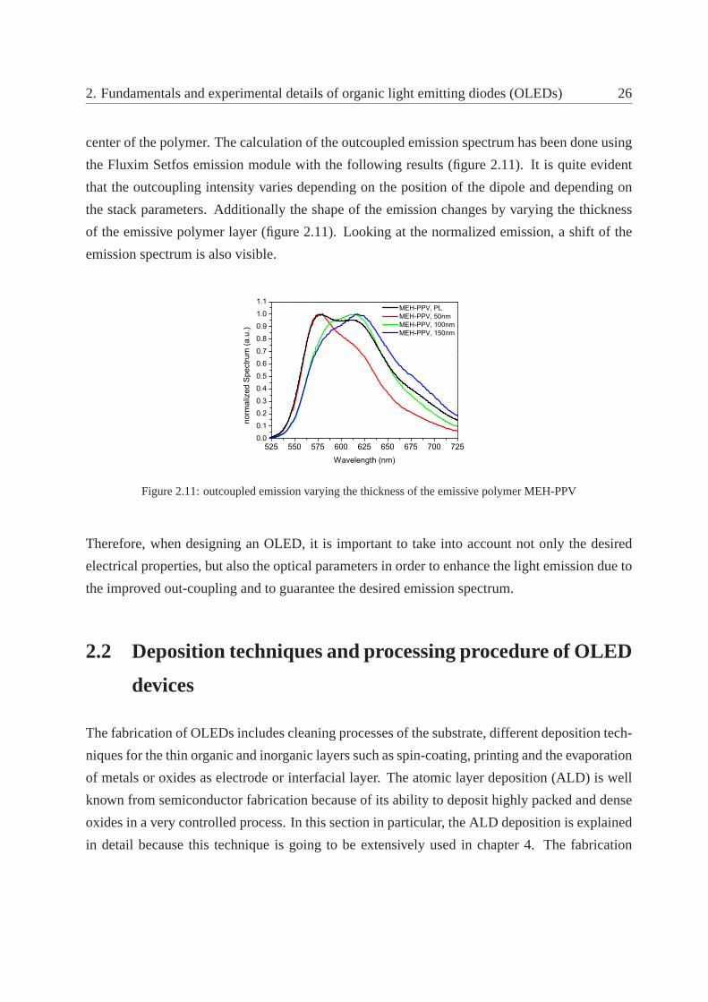
2. Fundamentals and experimental details of organic light emitting diodes (OLEDs) 26
center of the polymer. The calculation of the outcoupled emission spectrum has been done using
the Fluxim Setfos emission module with the following results (figure 2.11). It is quite evident
that the outcoupling intensity varies depending on the position of the dipole and depending on
the stack parameters. Additionally the shape of the emission changes by varying the thickness
of the emissive polymer layer (figure 2.11). Looking at the normalized emission, a shift of the
emission spectrum is also visible.
525 550 575 600 625 650 675 700 7250.0
0.1
0.2
0.3
0.4
0.5
0.6
0.7
0.8
0.9
1.0
1.1 MEH-PPV, PL MEH-PPV, 50nm MEH-PPV, 100nm MEH-PPV, 150nm
norm
aliz
ed S
pect
rum
(a.u
.)
Wavelength (nm)
Figure 2.11: outcoupled emission varying the thickness of the emissive polymer MEH-PPV
Therefore, when designing an OLED, it is important to take into account not only the desired
electrical properties, but also the optical parameters in order to enhance the light emission due to
the improved out-coupling and to guarantee the desired emission spectrum.
2.2 Deposition techniques and processing procedure of OLED
devices
The fabrication of OLEDs includes cleaning processes of thesubstrate, different deposition tech-
niques for the thin organic and inorganic layers such as spin-coating, printing and the evaporation
of metals or oxides as electrode or interfacial layer. The atomic layer deposition (ALD) is well
known from semiconductor fabrication because of its ability to deposit highly packed and dense
oxides in a very controlled process. In this section in particular, the ALD deposition is explained
in detail because this technique is going to be extensively used in chapter 4. The fabrication

2. Fundamentals and experimental details of organic light emitting diodes (OLEDs) 27
procedure of the different OLEDs devices processed within this research work is described as
well.
2.2.1 Atomic layer deposition
The Atomic layer deposition belongs to the chemical vapor deposition and is based on a self-
limiting surface reaction. The semiconductor industry is the main motivation for the recent ALD
development; however, there is a growing interest for the use of thin ALD deposited oxides
as encapsulation layer for organic devices. The ALD thin filmdeposition technique has been
widely used for example for the deposition of high dielectric constant gate oxides in MOSFET
structures. The advantage of ALD is the precise thickness control at the Ångstrom or monolayer
level. The self-limiting aspect of ALD leads to excellent step coverage and conformal deposition
on high aspect ratio structures [53]. ALD can be used to deposit several types of thin films,
including various oxides (e.g. Al2O3, TiO2, SnO2, ZnO, HfO2), metal nitrides (e.g. TiN, TaN,
WN, NbN), metals (e.g. Ru, Ir, Pt), and metal sulfides (e.g. ZnS)[54][55]. An example of the
excellent coverage of the ALD deposition is given in figure 2.12.
Figure 2.12: SEM image of a 300 nm Al2O3 film on a Si wafer taken from reference [56], courtesy of S. M. George
A commercial ALD reactor (the Savannah 300, Cambridge NanoTech) has been used for the
deposition of the Al2O3 layer. The deposition of a thin ALD layer typically involvesbasically
4 steps as explained for the deposition of the Al2O3. The precursor Trimethylaluminum (TMA)
will be injected into the vacuum reaction chamber resultingin a reaction with the available sur-
face groups of H2O. The self-limiting mechanism prevents further reactionson the surface due to
a high amount of precursor and/or due to the purging mechanism. The reaction chamber will be
purged by a gas N2 in the next step for removing all rest-products. After pumping the residues,

2. Fundamentals and experimental details of organic light emitting diodes (OLEDs) 28
the second injection of a precursor takes place again resulting in a chemical reaction with the new
groups on the surface. Another purging step concludes the ALD cycle, removes all the volatile
reaction byproducts and the excess of precursor present in the chamber. After one ALD cycle
(including the 4 steps) a monolayer of material is formed onto the substrate surface with identical
surface groups so that the same reaction can be started again.
The stabilization of the growth rate depends on the dose of the precursor. Initially the growth
rate is very low due to the low injection of the precursor and it increases when more precursor is
injected up to the self-limiting character. A stable deposition growth rate requires a very specific
temperature window, the so-called ALD window. Lower temperatures lead to higher growth rates
due to condensation of the precursor or even lead to lower growth rates due to insufficient thermal
energy as a requirement for the surface reaction. In the opposite way, higher temperatures might
lead to higher growth rates caused by increased gas phase reaction or eventually to lower growth
rates due to the partial decomposition of precursor molecules.
Despite this broad application field, there is still a lack ofunderstanding of the nucleation and
growth of Al2O3 ALD on polymers. ALD processes can be performed at relatively low tempera-
tures compared to standard CVD processes, thus significantlyenlarging the range of applications
especially in the field of polymer-based devices. It has beenshown that Al2O3 can be also
deposited at temperatures as low as 30C keeping most of the material properties, except the
density, which decreased significantly from 3.5 g/cm3 to 2.5 g/cm3 [57]. A longer cycle time is
required at lower process temperatures due to the slower reaction rate and lower vapor pressure
of the precursors. An increased purge is required in order toremove the remaining H2O in the
reaction chamber. The mechanism of the nucleation of the ALDlayer has been investigated in
several studies, especially when depositing on organic layers [56][58]. J. D. Fergusonet. al. ob-
served a migration of Al(CH3)4 reactant into polyethylene [59]. It has been proven furthermore
that the polyethylene particles are covered with an ALD film after 40 cycles. The diffusion effect
of the TMA into polymethylmethacrylate (PMMA), polypropylene, polystyrene, polyethylene,
and polyvinylchloride during cycling was extensively investigated in the work of C. A. Wilson
et. al. in 2005 [53]. The diffusion of the TMA is stronger during the first cycles and will be
hindered when the ALD begins to form a continuous film. The following picture illustrates the
migration of the ALD precursors into the organic layer (figure 2.13a), followed by the partial
coverage (figure 2.13b) until the ALD film prevents further migration (figure 2.13c) and finally
when a closed dense ALD layer has been grown (figure 2.13d).

2. Fundamentals and experimental details of organic light emitting diodes (OLEDs) 29
Figure 2.13: Schematic ALD deposition on polymer films, a.) polymer chains at the surface, b.) Al2O3 nucleation
clusters, c.) growing of a closed ALD film, d.) formation of a dense Al2O3 film (taking from [60], courtesy of S. M.
George)
The ALD process tool Savannah S300 from Cambridge Nanotech has been used throughout this
thesis. The Savannah is known as flow type reactor with a single gas injection and a single outlet
through which the reaction gases are pumped continuously. However, such a reactor might also
create a non-uniformity of the layer thickness since the gasflow is extremely directional atop
the substrate. The process of the atomic layer deposition takes place, as described before, in
cycles where each cycle is supposed to deposit 1.1 Å. The recipes for the process and for each
temperature are discussed and given by Cambridge Nanotech and shown in table 2.1.
Process Purge H2O Stop Purge TMA Stop
80 oC 0.015 s 30 s 0.015 s 30 s
150oC 0.015 s 20 s 0.015 s 20 s
235oC 0.015 s 5 s 0.015 s 5 s
Table 2.1: ALD process recipes for Al2O3 and one cycle
2.2.2 Measurement techniques
The thickness and the quality of the layers and their morphology and roughness have to be con-
trolled during the fabrication process using profilometer from KLA Tencor Alpha-Step IQ and
atomic force microscopy (AFM) from digital Instruments, Dimension D 3100S-1. The pro-
filometer is used to measure the thickness of the layer and to evaluate the quality, in terms of
roughness. In the case of the AFM, a tiny silicon needle is mounted on the cantilever. A de-
2. Fundamentals and experimental details of organic light emitting diodes (OLEDs) 30
flection of the needle takes place too and it is measured by a piezoelectric crystal. The AFM
analyzes the roughness as well as the morphology of the deposited layer. The AFM provides a
true three-dimensional surface profile allowing to obtain high resolution images, without requir-
ing any special treatments of the surface (such as metal/carbon coatings) that would irreversibly
change or damage the sample. The values for the roughness should be as low as possible in order
to avoid short circuits between layers and to obtain a uniform layer.
The optical properties of the organics are obtained by performing photoluminescence, absorp-
tion, reflection and transmission measurements. The optical bandgap of the polymer can be ob-
tained by measuring the absorption spectrum. Once this is known, the polymer can be excited at
the exact wavelength in order to obtain photoluminescent light emission. Such measurements are
also very important when trying to characterize polymer blends where optical interaction might
take place between the two entities of the blend. An example for this will be discussed in chapter
5. Photoluminescence measurements (PL) were done using a setup from an Olympus Micro-
scope (model BX51M). Various filters were used to select the specific wavelength regime of the
white light source. This wavelength regime corresponds to the specific absorption spectrum of
the polymers used in this thesis. The emitted light was then collected through an objective with
50 x magnification, then into an optical fiber coupled to a HR2000 spectrometer from OCEAN
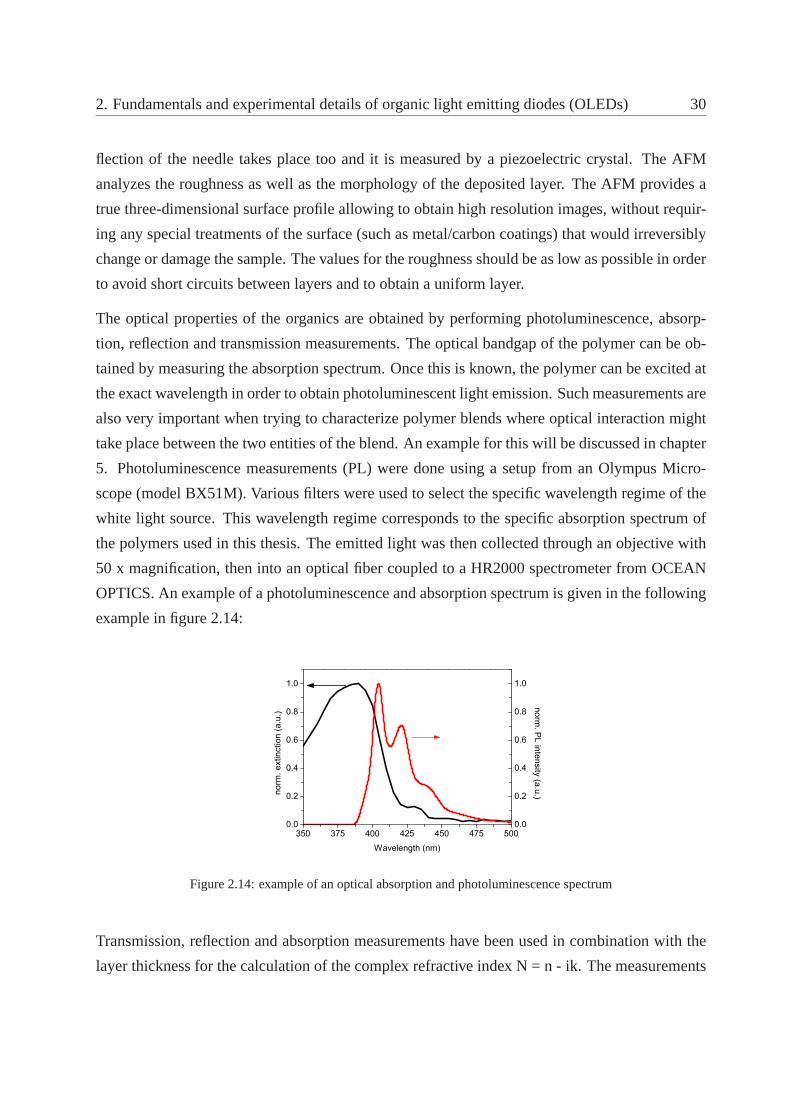
OPTICS. An example of a photoluminescence and absorption spectrum is given in the following
example in figure 2.14:
350 375 400 425 450 475 5000.0
0.2
0.4
0.6
0.8
1.0
norm. P
L intensity (a.u.)norm
. ext
inct
ion
(a.u
.)
Wavelength (nm)
0.0
0.2
0.4
0.6
0.8
1.0
Figure 2.14: example of an optical absorption and photoluminescence spectrum
Transmission, reflection and absorption measurements havebeen used in combination with the
layer thickness for the calculation of the complex refractive index N = n - ik. The measurements

2. Fundamentals and experimental details of organic light emitting diodes (OLEDs) 31
have been performed using the Varian Cary 5000 UV-Vis-NIR spectrometer with an attached
Ulbricht sphere for the measurement of the total emission.
An important parameter for light emitting organic materials is their quantum efficiency (quantum
yield), which is given by the ratio of the number of emitted photons to the number of photons
absorbed by the material. The quantum yield measurements were performed using the quantum
yield measurement system (C9920-02 from HAMAMATSU), for spin coated organic layers on
quartz substrates. The system is made up of an excitation light source that uses a xenon lamp
and a monochromator, an integration sphere and a multi-channel spectrometer. The integration
sphere is basically a hollow spherical cavity where the inside is covered with a diffuse reflective
coating. A detector which is attached on the sphere measuresthe emitted light without the effects
of beam shape, incident position and incident direction.
Electrical characterization allows to obtain the efficiency or performance of the fabricated de-
vices. The light intensity of a light source as perceived by the human eye is included when
referring the luminous intensity (photometric unit) measured in candela (cd). The maximum
spectral intensity of the human eye is described with 555 nm under daylight and shifts to 507 nm
under night light. Candela is a base unit defined as: a monochromatic light source emitting an
optical power of (1/683) W at 555 nm into the solid angle of 1 sr, which has a luminous intensity
of 1 cd. The luminous flux (known as the light power) is measured in lumen (lm) as is defined as:
a monochromatic light source emitting an optical power of (1/683) W at 555 nm has a luminous
flux of 1 lm. This means that 1 cd equals 1 lm/sr. An isotropic emitter with a luminous intensity
of 1 cd thus has a luminous flux of 4π lm. Furthermore, the luminance of an OLED (any sur-
face source) is defined as the ratio of the luminous intensityin a certain direction divided by the
projected surface area of that direction (cd/m2).
An example of the measured current density and luminance as afunction of the applied voltage
is shown in figure 2.15a. The efficiency of the measured OLED can be then calculated from the
current density and the luminance (2.15b).

2. Fundamentals and experimental details of organic light emitting diodes (OLEDs) 32
-2 -1 0 1 2 3 4 5 6 7 81E-5
1E-4
1E-3
0.01
0.1
1
10
100
1000
10000
Luminance (cd/m
2)
VTH
Cur
rent
den
sity
(A/m
2 )
Voltage (V)
1E-3
0.01
0.1
1
10
100
1000
10000
100000
(a)
2 3 4 5 6 7 8 9 10 11 120.1
1
10
Cur
rent
effi
cien
cy (c
d/A
)
Voltage (V)
0.1
1
10
Pow
er efficiency (lm/W
)
(b)
Figure 2.15: I/V and L/V characteristic (a), current and power efficiency (b)
The electrical characterization was done in a glove box system to protect the OLED from air as
the devices are not encapsulated. The devices were measuredwith a Keithley 236, 237 Source
Measure Units and a photodiode coupled to a Keithley 6485 picoampmeter, using a luminance
meter Minolta LS100 to calibrate the photocurrent. Two needles were contacted with the anode
and the cathode of the OLED and a voltage between -2V up to 20 V was applied. Both, the
current density (A/m2) and luminance (cd/m2) versus voltage curves were measured simultane-
ously. The threshold voltage VTH is defined as the voltage where the OLED starts to emit light
(see figure 2.14a).
The electroluminescence spectrum was measured with a HR2000spectrometer from OCEAN
OPTICS. The optical simulations have been performed using the emission module from Fluxim
Setfos package 3.3. All the materials used in this thesis have been characterized by their trans-
mittance and reflectance. The measured characteristics have been used for the calculation of the
refractive index n and absorption coefficient k using software developed by the University of
Potsdam (department Prof. Neher). The calculated constants have been included in the material
database of the simulation software. The software uses an algorithm based on the transfer-matrix
formalism for the simulation of the optical properties of the stack (see appendix).

Chapter 3
Ultra Thin Metal electrode for OLEDs
Nowadays ITO is widely used in research and industry as a semitransparent conductive electrode
material for OLEDs and solar cells. A semitransparent conductive electrode material requires
a low sheet-resistance, a high transmittance in the visiblelight spectrum, a work function, suit-
able for efficient charge injection. Fulfilling such requirements is complicated and although
ITO achieves most of them, it has also many drawbacks. It is wellknown that most of the light
is trapped inside the ITO layer which makes the light-outcoupling less efficient. Furthermore,
ITO contains indium, which is a rare and expensive material. The deposition on flexible plas-
tic substrates is problematic since ITO requires temperature treatments higher than 400C for
achieving a low sheet-resistance and high transmittance. Typical plastic substrates cannot be
treated at temperatures as high as required to achieve high quality ITO. Flexible substrates re-
quire mechanically stable materials, but ITO is brittle andbreaks upon bending. Using flexible
transparent substrates, however, is a strong motivation forthe commercialization of OLEDs.
Various types of doped oxides which do not contain cost intensive indium have been recently
investigated; among them, aluminum doped zinc oxide (AZO) [66] and gallium doped zinc oxide
(GZO) [67], which have promising material properties in terms of electrical conductivity, trans-
mittance, sheet resistance and the same efficiency has been reached as for ITO-based OLEDs
[68]. The light trapping mechanism [61], derived from the difference in refractive index between
the polymer/ ITO layer and the glass substrate, has been lowered through various approaches.
Nano-imprinted [62], nano-structured layers [62][63] or micro-lenses [64] have been shown to
decrease the high refractive index of the ITO resulting in anincreased outcoupling [65]. Oxide
33

3. Ultra Thin Metal electrode for OLEDs 34
based electrodes have to be relatively thick due to the required low sheet resistance. However,
using thick layers usually leads to a lower outcoupling efficiency. As proposed by a number
of research groups [69][70][71], carbon nanotubes (CNTs), when processed as thin films, are
suitable for replacing ITO in OLED technology for flexible applications, because CNTs hold key
properties such as flexibility and transparency. Overcoming the relatively high sheet-resistance,
reproducibility and the quite complex surface functionalization is a focus of the research nowa-
days. A complete oxide and indium free anode has been proposed by Meiss et al [72] where a
multilayer contact made of ultra-thin thermally evaporated Al and Ag films was used for organic
solar cell application with an achieved efficiency up to 2.2% . A solution for an ITO and TCO
free device was presented by H. Peng et al [74] where they proposed a simple thin silver (Ag)
layer as semitransparent anode contact.
Ni as ultra-thin metal for optoelectronic applications has been developed [75]. It was shown
that a similar device performance can be obtained when using Nias anode material instead
of ITO [76], even though the transmittance of the ultrathin Nilayer is poor when compared to
ITO. A further improvement in terms of transmittance and sheet resistance for the metal anode
has been obtained when using Cu capped with Ni, combining the low sheet-resistance and high
transmittance of Cu with the high work-function and stability of Ni [77].
3.1 Experimental details
For the OLED fabrication, glass plates either covered with Indium-tin-oxide (100 nm ITO with
13 Ω/sq, Labor für Bildschirmtechnik, University Stuttgart) ormetal such as Ni, CuNi, Cu
(ICFO, optoelectronic group led by V. Pruneri) were cleaned for 10 min in Methanol using an
ultrasonic bath. The deposition was performed with a DC voltage sputtering machine Kenosistec
Dual Chamber at room temperature and in pure Ar atmosphere on double-side optically polished
UV grade silica substrates. In all cases a DC power of 200 W anda pressure during deposition
of 8 x 10⁻³ Torr have been used. The thickness was calculated based on the deposition rate,
which in turn was determined by an MCM-160 quartz crystal. Theresulting deposition rate for
the single Ni layer was 1.6 Å/s. The deposition rates for the CuNi double layer were 1.5 and 0.57
Å/s for Cu and Ni, respectively. Afterwards, the samples werefirst rinsed in water, then dried
with Nitrogen and finally heated and dried for 10 min at 120C. The samples were exposed
by an ozone treatment for 10 min just before the deposition ofthe PEDOT:PSS (Clevios P VP

3. Ultra Thin Metal electrode for OLEDs 35
Al 4083) hole injection organic film. The measured thicknessof the PEDOT:PSS layer was 25
nm using a spin-coating recipe with no ramp time and 6000 rpm for 40 s followed by a postan-
nealing process for 30 min at 120C. Two polymers (SY and PFO) as emissive layer have been
sandwiched in the device structure, while the transparent conductive bottom electrode material
has been varied. Poly(phenylenevinylene) co-polymer (SY), from MERCK, was dissolved in
Toluene (5 mg/ml) and stirred overnight. Poly(9,9-dioctylfluorene) (PFO) was purchased from
H. W. Sands and dissolved with a concentration of 7 mg/ml chloroform (CHCl3) and finally fil-
tered with a 1µm filter. The samples spin-coated with SY were additionally heated for 10 min
at 120C due to the higher boiling point of Toluene (111C). The spin-coating recipe and the
corresponding thickness vary depending on the concentration and material used. The recipes are
summarized in table 3.1.:
Polymer Concentration Solvent Spincoating Recipe Thickness
PFO 7 mg/ml CHCl3 -/1500/20 70 nm
SY 5 mg/ml Toluene -/2500/20 80 nm
Table 3.1: Polymer solution concentration, spin-coating recipe and resulting thickness
Different electrodes have been used in this study. Thermally evaporated (<5 x 10⁻⁶ mbar) Al or
CaAg films (100 nm) were used as single or double layer cathodesfor the devices. A shadow
mask with a circular electrode has been used (12.6 mm2). The following device architectures
have been used in this chapter:
(a) (b) (c)
Figure 3.1: (a) Variation of the Ni thickness for PFO-based OLEDs, (b) with PFO and Ca as electron injection layer
and (c) SY-based OLEDs with ITO, Ni, Cu, CuNi as anode (thickness of 8 nm)

3. Ultra Thin Metal electrode for OLEDs 36
3.2 Characterization of the ultra thin metal electrodes
Metal films as bottom electrode contacts have excellent electronic properties due to high con-
ductivity. Metals can be easily processed and patterned by various techniques. Despite all ad-
vantages, metal films with a thickness of only 20 nm are mostlyopaque. L. Martínezet.al. [78]
demonstrated that ultrathin-Ni films show promising results in terms of film continuity and sheet-
resistance, although the transmittance was lower than for the ITO. In this section, the ultrathin
Ni-films have been studied in detail and applied as semitransparent anode in OLEDs. Four dif-
ferent deposition times for the Ni process were chosen in this section and the resulting thickness
was calculated from the deposition rate and the deposition time; 6 nm (75 s), 7.2 nm (90 s), 8.5
nm (105 s), 9.5 nm (120 s). The conductivity and transmissionof ultrathin Ni-films have been
compared to those of commercially available ITO. The sheet-resistance is shown as a function of
the Ni thickness in figure 3.2.
5.5 6.0 6.5 7.0 7.5 8.0 8.5 9.0 9.5 10.0 10.5 11.020
30
40
50
60
70
80
90
She
et re
sist
ance
(/s
q)
Ni thickness (nm)
Figure 3.2: Sheet Resistance vs. layer thickness of the Ni layer (Courtesy of D. S. Ghosh)
The sheet resistance was higher for the best Ni-film (30Ω/sq) than for ITO (14Ω/sq) [78] film.
It can be also seen that the sheet resistance is lower for thicker Ni layers. The sheet resistance is
analogous to resistivity when using a three-dimensional system with a planar current flow. The
resistance can be therefore written as shown in equation 3.1:
R=ρLtW
= RsLW
(3.1)
where R is the resistance, L is the length, t is the thickness and W refers to the width of the cross
3. Ultra Thin Metal electrode for OLEDs 37
sectional area. A common term for the definition of the electrical properties isΩ/sq, which is
dimensionless and is exclusively used for sheet resistance(with L = W and Rs = R) [79]. The
transmittance and reflectance of Ni layers with a thickness of 8.5 nm and 9.5 nm have been
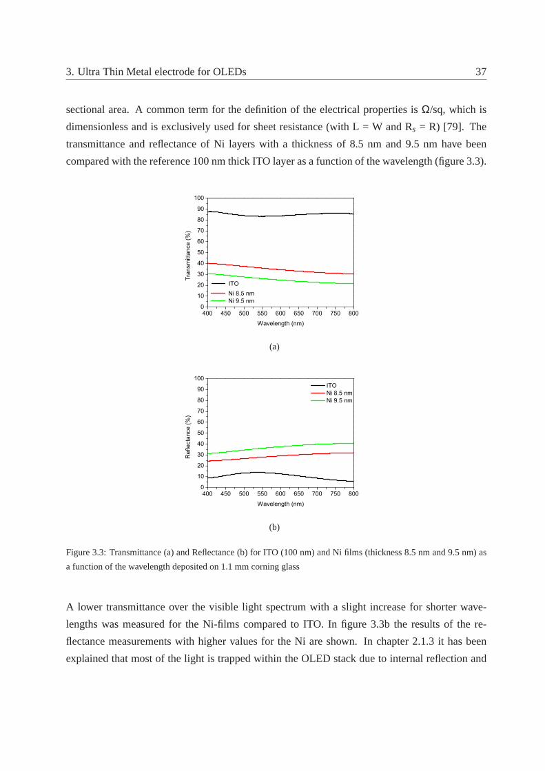
compared with the reference 100 nm thick ITO layer as a function of the wavelength (figure 3.3).
400 450 500 550 600 650 700 750 8000
10
20
30
40
50
60
70
80
90
100
Ni 8.5 nm Ni 9.5 nm
Tra
nsm
ittan
ce (%
)
Wavelength (nm)
ITO
(a)
400 450 500 550 600 650 700 750 8000
10
20
30
40
50
60
70
80
90
100 ITO Ni 8.5 nm Ni 9.5 nm
Ref
lect
ance
(%)
Wavelength (nm)
(b)
Figure 3.3: Transmittance (a) and Reflectance (b) for ITO (100 nm) and Ni films (thickness 8.5 nm and 9.5 nm) as
a function of the wavelength deposited on 1.1 mm corning glass
A lower transmittance over the visible light spectrum with aslight increase for shorter wave-
lengths was measured for the Ni-films compared to ITO. In figure 3.3b the results of the re-
flectance measurements with higher values for the Ni are shown. In chapter 2.1.3 it has been
explained that most of the light is trapped within the OLED stack due to internal reflection and

3. Ultra Thin Metal electrode for OLEDs 38
the different dielectric constants of the materials used. It is therefore mandatory to keep the re-
flectance of the semitransparent electrode as low as possible so that the outcoupling of the light
is not hindered [80].
The surface roughness has to be kept below the thickness of the layer, otherwise films could be
discontinuous and thus non-conductive. Impurities and contaminants are likely to be the most
important source of defects. The fabricated Ni thin layers were characterized by atomic force
microscopy (AFM). The analysis revealed that the surface ofthe Ni layer is homogeneous and
flat for all thicknesses (figure 3.4). In general, the roughness of the Ni layer increases with
thickness and is for each film thickness higher than that of ITO, which is around 0.5 nm.
(a) (b)
Figure 3.4: AFM pictures from ITO (a) and Ni = 9.5 nm (b)
The measurement of the work-function of the Ni films was also carried out and listed in table
3.2. A work-function of 5 eV for the ITO film and a work-function of 5.4 eV for the 6 nm and
5.1 eV for thicker layers have been measured by ultraviolet photoelectron spectroscopy (UPS).
Hung et. al. demonstrated that the workfunction might change for ultrathin metal film due
to the irregular islandic growth of metals. The workfunction for layer thicknesses close to the
percolation thickness of around 2 - 5 nm differs therefore, compared to the continuous film [81],
which explains probably the higher workfunction of the lowest Ni thickness. The percolation
of metals ranges between 2 and 6 nm depending on process and process conditions. Another
explanation has been found for double metal layers [82] The dependence of the workfunction
has been attributed to interfacial issues due to resistivity differences of the metallic films. This is
even more significant in the case where the film thickness is close to the percolation thickness.

3. Ultra Thin Metal electrode for OLEDs 39
Material and Thickness (nm) ITO (100) Ni (6) Ni (7.2) Ni (8.5) Ni (9.5)
Transmittance (%) 86 40 35 31 29
Rs (Ω/sq) 14 80 62 51 33
ϕ =T10
AvRS
15.8 x 10⁻³ 1.31 x 10⁻⁶ 0.44 x 10⁻⁶ 0.16 x 10⁻⁶ 0.13 x 10⁻⁶
Workfunction (eV) 5.0 5.4 5.1 5.1 5.1
RMS (nm) 0.5 not carried out 1 1.5 2.2
Table 3.2: Mean optical transmission and sheet resistance with deposition time of the nickel films. The Haacke
figure of merit was calculated from the average transmittance and the sheet resistance [83]
The values in table 3.2 show, the best figure of merit for the Nilayer is obtained for the highest
transmittance even though the sheet resistance is the lowest. It is therefore important to increase
the transmittance to reach a better figure of merit.
To summarize, Ni as ultra-thin metal film shows good material properties in terms of low sheet-
resistance and low roughness. The films were shown to be continuous by AFM. Furthermore,
it was found that the work function matches quite well the workfunction of the commonly used
ITO electrode material. The transmittance is constant in the visible spectrum although the trans-
mittance is lower than for the ITO. The reasonable electricalproperties of the ultra-thin Ni film
might be useful for the application of such metal films as semitransparent electrode for OLED
application even though the transmittance is rather low. The outcoupling efficiency depends on
both, the transmittance and the thickness of the layer. The single Ni layer is therefore applied
as conductive and semitransparent electrode in the following subchapters in order to investigate
the influence of the UTMF on the outcoupling and finally on the overall OLED performance.
Further work is conducted in the subchapter 3.4 to decrease the sheet resistance and to increase
the transmittance.
3.3 Nickel UTMF as bottom anode for OLEDs
The UTMF-Ni layer was characterized in the previous sectionand is applied as semitransparent
electrode material in bottom-emitting OLEDs in the following section varying the thickness of
the Ni-film. The OLEDs were optimized further, depositing a commonly used electron injection
layer (Ca) between the polymer and the cathode. OLEDs based onblue (PFO) and red (SY)
emitting polymers were fabricated and characterized.

3. Ultra Thin Metal electrode for OLEDs 40
3.3.1 Influence of the Ni layer thickness on the performance of OLEDs
The variation of the electrical and optical properties withthe thickness of the ultra-thin-Ni layer
has been studied in the previous section. Now the influence ofthe metal anode thickness on the
OLED performance has been investigated. Ultra-thin Ni layers have been used as semitranspar-
ent anode material in a bottom light emission OLED configuration. The used device structure
(ITO,Ni/PEDOT:PSS/PFO/Al) and the corresponding energy levels are shown in figure 3.5.
Figure 3.5: OLED schematic (a) and energy band diagram (b)
The device structure in figure 3.5 favors holes as majority charge carrier because of the large
energy gap between the Al-cathode and the LUMO level of the polymer. Thus, the injection of
the electrons is hindered (figure 3.5b). The device efficiency is therefore expected to be low. As
mentioned in the introduction, the main focus of this thesisis to find new concepts (and not to
point efficiency records).
Photoluminescence measurements are mandatory in order to check the quality of the spin-coated
polymer film and whether the Ni-roughness affects the morphology of the deposited polymer
layer. The PL spectra of the ITO and the Ni OLED have been measured at different positions at
the device configuration due to the difference in reflectanceand transmittance spectrum of the
ITO and the Ni. The positions for the measurements are shown in figure 3.6.

3. Ultra Thin Metal electrode for OLEDs 41
Figure 3.6: Positions of the PL measurements position
The figures 3.7 below show the emission spectrum from the PFO film spin coated on ITO and
on Ni (8.5 nm). The emission spectra are very similar and showthree sharp peaks at 440 nm,
470 nm and 490 nm. Those values correspond to the singlet intrachain excitons where the most
intensive first peak at 440 nm refers to the electronicπ∗−π transition [84].
400 425 450 475 500 525 550 575 6000.00.10.20.30.40.50.60.70.80.91.01.1
PFO on ITO PFO on Ni (8.5 nm)
norm
. PL
inte
nsity
(a.u
.)
Wavelength (nm)
(a) PL spectrum from the Top
400 425 450 475 500 525 550 575 6000.00.10.20.30.40.50.60.70.80.91.01.1
PFO on ITO PFO on Ni (8.5 nm)
norm
. PL
inte
nsity
(a.u
.)
Wavelength (nm)
(b) PL spectrum from the Bottom
400 425 450 475 500 525 550 575 6000.00.10.20.30.40.50.60.70.80.91.01.1
PFO on ITO PFO on Ni (8.5 nm)
norm
. PL
inte
nsity
(a.u
.)
Wavelength (nm)
(c) PL spectrum below Al-cathode
Figure 3.7: PL spectrum for Ni/ITO OLED has been taken from the top (a), from the bottom (b) and from the bottom
just below the cathode of the OLED (c)
However, the emission wavelength is not only regarded to theemission of the polymer, but also
to the optical characteristic of the stack. Therefore, the outcoupled spectrum might differ from
the pure emission spectrum of the polymer which has been alsodescribed in equation 2.13 in
the theoretical chapter. Almost no difference can be observed when measuring the PL spectrum
from the top (figure 3.7a), since the effect of the reflection coming from Ni and ITO on the emis-
sion spectrum of the polymer is very low. The PL spectrum has been taken from the top, which
means the measured light does not have to travel through a stack of layers with different optical

3. Ultra Thin Metal electrode for OLEDs 42
properties for each layer as it was observed for the measurement configuration in figure 3.7b.
The refractive index as well as the absorption coefficient varies in dependence to the wavelength.
For the PL spectrum (and later for the EL spectrum) all these parameters have to be considered
when evaluating the Ni-anode as possible replacement for ITO. The recorded PL spectrum looks
different, which might be due to the influence of the optical stack on the emission of the poly-
mer. The emitted light has to travel from the PFO through the PEDOT:PSS (25 nm), the anode
material (either ITO (100 nm) or Ni (8.5 nm)) and through the glass substrate (1.1 mm). The low
outcoupling efficiency of OLEDs has been explained in the theoretical chapter with the result
that most of the light will be trapped inside the OLED stack and guided either to the edges of the
OLED or absorbed within the stack. The different modes are wavelength dependent and they are
related to the reflectance, absorbance and transmittance characteristic over the wavelength for
each material used in this OLED stack [85]. An even stronger difference of the emission spec-
trum for the ITO and Ni has been observed in figure 3.7c. The emitted light will be nearly 100
% reflected by the Al-back electrode and will travel again through the stack overlapping the pure
emission spectrum coming from the polymer. Such a behavior is closely related to the guidance
of the light when the OLED is electrically excited. It is therefore expected that the out-coupled
electroluminescence spectrum will differ from the photoluminescence spectrum, especially for
the vibronic replica.
The current density, luminance and the power efficiency as a function of voltage have been
measured for the uncapsulated OLEDs (figure 3.8a-c). The injection of electrons is unlikely to
be efficient given the estimated energy gap of 1.6 eV between the work-function of the Al and
the LUMO level of the polymer. Apart from the thickest Ni layer device (9.5 nm), in general, the
Ni-based devices show lower current densities and higher voltage thresholds than the ITO-based
device (figure 3.8a). In general, the Ni layers show a higher sheet resistance than ITO resulting
in higher required threshold voltages. It has been reportedthat the current density in the ohmic
regime at low voltages is determined by the anode contact properties rather than by organic bulk
properties [86]. The surface roughness influences also the current density by changing the total
effective area of contact [87]. Y. - R. Jenget. al. [87] has shown that this additional effect
plays a more significant role at initial and low voltages. Thehigher sheet resistance for low Ni
thicknesses limits therefore the device performance in terms of threshold voltage and the voltage
at maximum brightness.
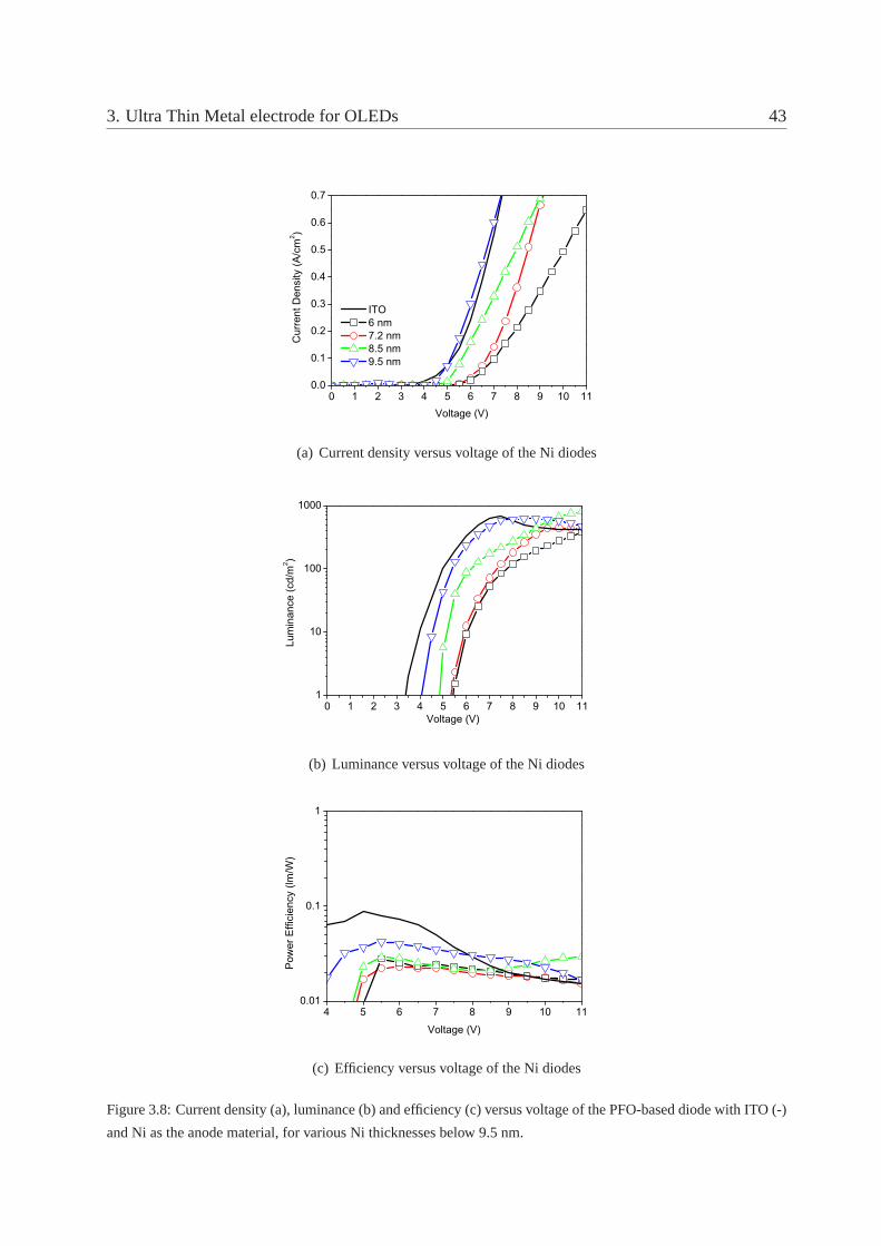
3. Ultra Thin Metal electrode for OLEDs 43
0 1 2 3 4 5 6 7 8 9 10 110.0
0.1
0.2
0.3
0.4
0.5
0.6
0.7
ITO 6 nm 7.2 nm 8.5 nm 9.5 nm
Cur
rent
Den
sity
(A/c
m2 )
Voltage (V)
(a) Current density versus voltage of the Ni diodes
0 1 2 3 4 5 6 7 8 9 10 111
10
100
1000
Voltage (V)
Lum
inan
ce (c
d/m
2 )
(b) Luminance versus voltage of the Ni diodes
4 5 6 7 8 9 10 110.01
0.1
1
Pow
er E
ffici
ency
(lm
/W)
Voltage (V)
(c) Efficiency versus voltage of the Ni diodes
Figure 3.8: Current density (a), luminance (b) and efficiency (c) versus voltage of the PFO-based diode with ITO (-)
and Ni as the anode material, for various Ni thicknesses below 9.5 nm.
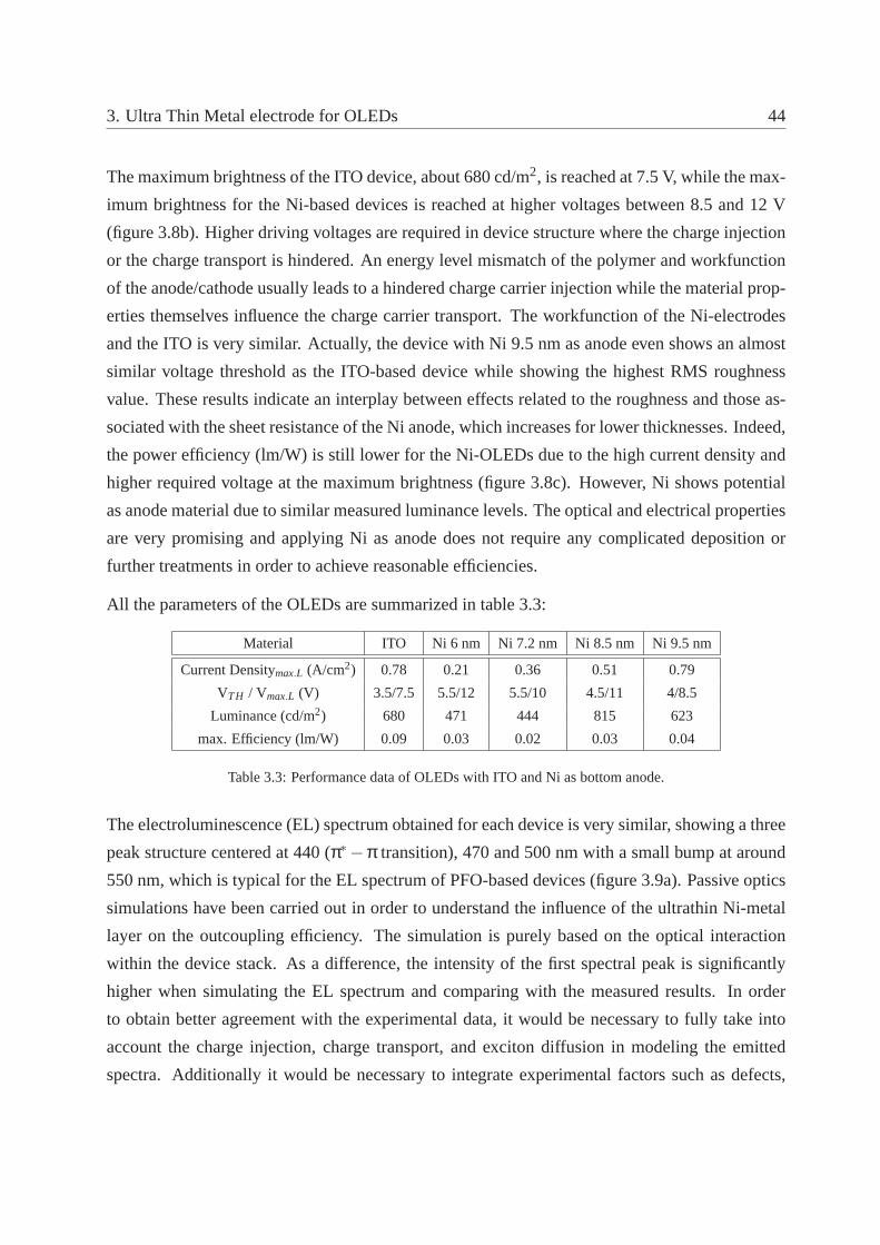
3. Ultra Thin Metal electrode for OLEDs 44
The maximum brightness of the ITO device, about 680 cd/m2, is reached at 7.5 V, while the max-
imum brightness for the Ni-based devices is reached at higher voltages between 8.5 and 12 V
(figure 3.8b). Higher driving voltages are required in device structure where the charge injection
or the charge transport is hindered. An energy level mismatch of the polymer and workfunction
of the anode/cathode usually leads to a hindered charge carrier injection while the material prop-
erties themselves influence the charge carrier transport. The workfunction of the Ni-electrodes
and the ITO is very similar. Actually, the device with Ni 9.5 nm as anode even shows an almost
similar voltage threshold as the ITO-based device while showing the highest RMS roughness
value. These results indicate an interplay between effectsrelated to the roughness and those as-
sociated with the sheet resistance of the Ni anode, which increases for lower thicknesses. Indeed,
the power efficiency (lm/W) is still lower for the Ni-OLEDs dueto the high current density and
higher required voltage at the maximum brightness (figure 3.8c). However, Ni shows potential
as anode material due to similar measured luminance levels.The optical and electrical properties
are very promising and applying Ni as anode does not require any complicated deposition or
further treatments in order to achieve reasonable efficiencies.
All the parameters of the OLEDs are summarized in table 3.3:
Material ITO Ni 6 nm Ni 7.2 nm Ni 8.5 nm Ni 9.5 nm
Current Densitymax.L (A/cm2) 0.78 0.21 0.36 0.51 0.79
VTH / Vmax.L (V) 3.5/7.5 5.5/12 5.5/10 4.5/11 4/8.5
Luminance (cd/m2) 680 471 444 815 623
max. Efficiency (lm/W) 0.09 0.03 0.02 0.03 0.04
Table 3.3: Performance data of OLEDs with ITO and Ni as bottomanode.
The electroluminescence (EL) spectrum obtained for each device is very similar, showing a three
peak structure centered at 440 (π∗−π transition), 470 and 500 nm with a small bump at around
550 nm, which is typical for the EL spectrum of PFO-based devices (figure 3.9a). Passive optics
simulations have been carried out in order to understand theinfluence of the ultrathin Ni-metal
layer on the outcoupling efficiency. The simulation is purely based on the optical interaction
within the device stack. As a difference, the intensity of the first spectral peak is significantly
higher when simulating the EL spectrum and comparing with the measured results. In order
to obtain better agreement with the experimental data, it would be necessary to fully take into
account the charge injection, charge transport, and exciton diffusion in modeling the emitted
spectra. Additionally it would be necessary to integrate experimental factors such as defects,
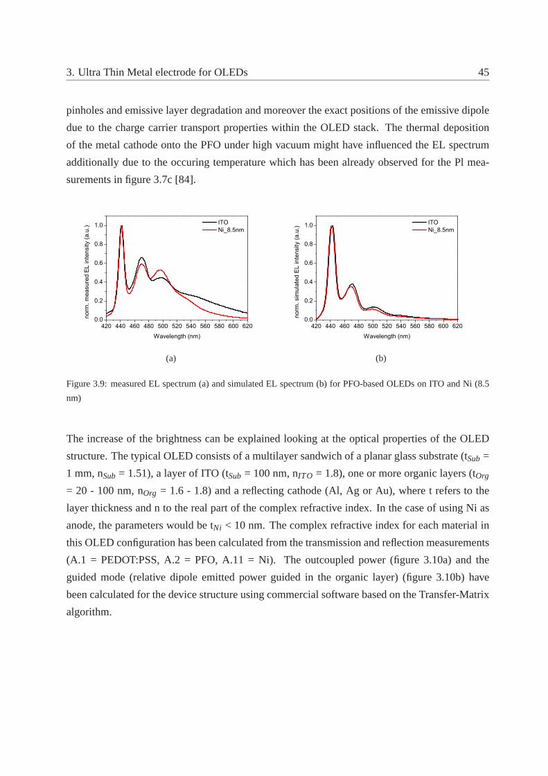
3. Ultra Thin Metal electrode for OLEDs 45
pinholes and emissive layer degradation and moreover the exact positions of the emissive dipole
due to the charge carrier transport properties within the OLED stack. The thermal deposition
of the metal cathode onto the PFO under high vacuum might haveinfluenced the EL spectrum
additionally due to the occuring temperature which has beenalready observed for the Pl mea-
surements in figure 3.7c [84].
420 440 460 480 500 520 540 560 580 600 6200.0
0.2
0.4
0.6
0.8
1.0 ITO Ni_8.5nm
norm
. mea
sure
d E
L in
tens
ity (a
.u.)
Wavelength (nm)
(a)
420 440 460 480 500 520 540 560 580 600 6200.0
0.2
0.4
0.6
0.8
1.0 ITO Ni_8.5nm
norm
. sim
ulat
ed E
L in
tens
ity (a
.u.)
Wavelength (nm)
(b)
Figure 3.9: measured EL spectrum (a) and simulated EL spectrum (b) for PFO-based OLEDs on ITO and Ni (8.5
nm)
The increase of the brightness can be explained looking at the optical properties of the OLED
structure. The typical OLED consists of a multilayer sandwich of a planar glass substrate (tSub=
1 mm, nSub= 1.51), a layer of ITO (tSub= 100 nm, nITO = 1.8), one or more organic layers (tOrg
= 20 - 100 nm, nOrg = 1.6 - 1.8) and a reflecting cathode (Al, Ag or Au), where t refers to the
layer thickness and n to the real part of the complex refractive index. In the case of using Ni as
anode, the parameters would be tNi < 10 nm. The complex refractive index for each material in
this OLED configuration has been calculated from the transmission and reflection measurements
(A.1 = PEDOT:PSS, A.2 = PFO, A.11 = Ni). The outcoupled power (figure 3.10a) and the
guided mode (relative dipole emitted power guided in the organic layer) (figure 3.10b) have
been calculated for the device structure using commercial software based on the Transfer-Matrix
algorithm.

3. Ultra Thin Metal electrode for OLEDs 46
420 440 460 480 500 520 540 560 580 600 6200
2
4
6
8
10 ITO Ni_8.5 nm
outc
oupl
ed fr
actio
n of
tota
l Pow
er (%
)
Wavelength (nm)
(a)
420 440 460 480 500 520 540 560 580 600 6200
4
8
12
16
20
ITO Ni_8.5 nm
Gui
ded
mod
e fra
ctio
n of
tota
l pow
er (%
)
Wavelength (nm)
(b)
Figure 3.10: out-coupled (a) and guided mode (b) fraction ofthe total emitted power for ITO and Ni OLED
The average outcoupling and guided mode fraction of the total emitted power by the dipole have
been calculated using the photoluminescence spectrum of the PFO between 420 and 620 nm. The
calculated outcoupled fraction of the total power for the ITO-OLED for the given wavelength
range is around 5.6 % which is significantly lower than for theNi-OLED (Ni thickness 8.5 nm)
with 7.3 %. Figure 3.10a does not explain the reason for the lower outcoupling efficiency of the
ITO-OLED, but shows the variation of the outcoupling power over the wavelength as a result
of the wavelength dependence of the refractive index. Figure 3.10b demonstrates the possible
reason for the increase of the outcoupling efficiency of the Ni layer even though the transmittance
is much lower. It shows a significant drop of the guided mode intensity defined as the relative
dipole emitted power guided in the organic layers due to the refractive index difference between
the organic layer and the electrode.
Very significant for the lower outcoupled power of the ITO is difference of the dipole emitted
power lost in guided modes. The simulated guided modes are relatively constant over the emis-
sion wavelength of the polymer even with a slight increase for longer wavelength. The opposite
behavior has been observed for this particular device configuration for the Ni device. The power
lost into guided modes drops from an initial high value at shorter wavelengths to very low values.
The ITO outcoupling efficiency suffers therefore due to the presence of high losses due to the
guided modes, in particular at the emission wavelength of the PFO as active material. Again, the
outcoupling efficiency has to be calculated and optimized for each specific device structure and
each specific emissive polymer since the optical propertiesof the stack are wavelength depen-

3. Ultra Thin Metal electrode for OLEDs 47
dent. The electrical properties in terms of workfunction and dipole position have been considered
to be the same for all the devices.
The outcoupled power as a fraction of the total power emittedby the dipole has been simulated
for a Ni layer thickness between 3 and 20 nm (figure 3.11). The device configuration including
the simulation parameters (dipole position, quantum efficiency of the polymer) was identical as
before. The thicker the Ni electrode, the lower the outcoupled power. The highest outcoupled
power has been simulated for the emission wavelength regimeof the polymer, between 430 and
490 nm, and a Ni layer thinner than 10 nm, which again confirms the previous results.
Outc
ouple
d fra
ction o
f tota
l pow
er
(%)
1.5
8.5
9.5nm
8.5nm
7.2nm
6.0nm
440nm 470nm 500nm
Figure 3.11: outcoupled fraction of the total emitted powerin dependence of the Ni thickness for the emission
spectrum of PFO, the used Ni thickness and the characteristic maxima at 440 nm, 470 nm and 500 nm for the PFO
emission are indicated
To conclude, it has been demonstrated that ultrathin Ni films can be easily fabricated without
having any post process and still reach reasonable values interms of electrical and optical
properties. Ultrathin Ni-film have been applied as semitransparent conductive anode contact for
bottom light emitting OLEDs. Despite the fact that thin Ni-layers have a lower transmittance,
higher roughness and a higher sheet resistance compared to ITO films, the device efficiency
was reasonably good when compared to that of the ITO-based device showing the potential
of Ni as anode material. The simulation has shown that the outcoupling intensity of the Ni-
based OLEDs is higher than for the ITO due to a low guided mode intensity, which explains the

3. Ultra Thin Metal electrode for OLEDs 48
similar luminance level even though the transmittance of the Ni layer is lower. Ultrathin Ni films
show therefore a significant potential as low cost and easy processable semitransparent anode
material.
3.3.2 Increased efficiency of Ni-OLEDs due to improved electron injection
The charge injection is very crucial for an efficient functioning of OLEDs with the aim of obtain-
ing a balanced charge injection for both, holes and electrons. Usually calcium (Ca), magnesium
(Mg) or barium (Ba) are used as interfacial layer between the polymer and the metal electrode
to improve the electron injection [89]. A poor electron injection might have lead in the previous
section to an unbalance of electrons and holes resulting in apoor OLED efficiency. Therefore,
a 20 nm thin Ca layer was deposited as interfacial layer between the polymer and the cathode
metal to improve the overall efficiency. The device architecture (Anode/ PEDOT/ PFO/ Ca/ Ag)
and the proposed band diagram are shown in figure 3.11.
(a) (b)
Figure 3.12: Schematic of PFO-based OLEDs (a) with Ca as interfacial layer and corresponding band diagram (b)
As expected, the overall efficiency is higher for the OLEDs with calcium as interfacial layer due
to the improved charge carrier balance since more electronsare injected. The current density is
lower and furthermore the threshold voltage has been significantly decreased, as represented in
figure 3.12.

3. Ultra Thin Metal electrode for OLEDs 49
0 1 2 3 4 5 6 7 8 90.00
0.05
0.10
0.15
0.20
0.25
0.30
0.35
0.40 ITO Ni_10 nm
Cur
rent
Den
sity
(A/c
m2 )
Voltage (V)
0.1
1
10
100
1000
10000
Luminance (cd/m
2)
(a)
4.0 4.5 5.0 5.5 6.0 6.5 7.0 7.5 8.0 8.5 9.00.01
0.1
1
ITO Ni _10 nm
Pow
er E
ffici
ency
(lm
/W)
Voltage (V)
(b)
Figure 3.13: measured OLED characteristics for devices with PFO as active polymer and CaAg cathodes, current
density and luminance level (a) and power efficiency (b)
The measured brightness for the Ni-based OLED is indeed up to45 % higher than for the ITO-
OLEDs. Also the threshold voltage (measured at 1 cd/m2) has been improved and is with 4.5
V slightly lower than for the ITO (5 V). The required voltage at the maximum light emission
for the best Ni-OLED is also 0.6 V lower than for the ITO. Thosetwo factors have a significant
influence on the power efficiency resulting in a strong increase of the power efficiency for the
Ni-OLED, almost 3 times of that one of the ITO. The table 3.4 shows the measured values for all
Ni-based OLEDs; the applied voltage at the maximum brightness, the threshold voltage for light
emission at 1 cd/m2, the maximum brightness and the calculated power efficiency.
ITO Ni 6 nm Ni 8 nm Ni 10 nm
max. Luminancemax.J (cd/m2) 1317 1106 1165 1970
Current Densitymax.L (A/m2) 0.59 0.41 0.45 0.55
VTH / Vmax.L (V) 5/9.7 5.1/11.8 5.3/10.3 4.5/9.1
max. Efficiency (lm/W) 0.08 0.15 0.14 0.24
Table 3.4: Performance data of the PFO-OLEDs with ITO and Ni anode and CaAg as cathode. The current
densitymax.L and Vmax.L has been measured at the maximum luminance before the OLED starts to degrade. The
current density and luminance differ at the in the table given maximum efficiency.
As indicated, the supposedly increased injection of electrons might shift the recombination zone
away from the cathode towards the center of the polymer [90].The emitter dipole position
within the emissive layer has been calculated taking into accout the device stack parameters and

3. Ultra Thin Metal electrode for OLEDs 50
the measured PL/ EL spectrum. The simulation proves that therecombination zone is shifted
from the position close to the CaAg - cathode towards the PEDOT:PSS - PFO interface. A
dipole position at around 61 nm (close to the Al-cathode) hasbeen calculated for the previous
OLED structure without Ca while the dipole position is shifted to be at 19 nm (close to the
PEDOT:PSS-PFO interface) for the present configuration. Shifting the emitter dipole away from
the metal cathode leads to lower losses due to evanescently coupled modes. The simulation in
figure 3.14 shows the calculated fraction of power lost in thedevice due to evanescently coupled
modes, waveguiding modes, absorption losses and non-radiative power losses (measured PL
quantum efficiency of 57 %) and the finally outcoupled power asa function of the emissive
dipole position. The highest outcoupling intensity can be obtained when the emissive dipole is
close to the center of the emissive polymer. The electrical parameters, such as VTH and current
density, are mostly influenced by the improved injection andimproved charge carrier balance.
Both effects together increase the power efficiency (lm/W) of the OLED device.
Figure 3.14: relative average power contribution, outcoupled power (red), substrate guided mode (blue), absorption
losses in the organic stack (yellow), waveguiding modes (violett) and non-radiative losses (pink) depending on the
relative emitter dipole position. An emitter dipole position of "‘0"’ indicates a position at the PEDOT:PSS polymer
interface while a relative position of "‘1"’ refers to the Polymer - CaAg cathode interface
The shift of the emissive dipole towards the PEDOT:PSS-PFO interface influences additionally
the outcoupled emission spectrum. A significant change can be seen for the electroluminescence
of these OLEDs compared to the previous study shown in the recorded electroluminescence
spectra. The comparison can be seen in figure 3.15.

3. Ultra Thin Metal electrode for OLEDs 51
400 425 450 475 500 525 550 575 600 625 6500.0
0.2
0.4
0.6
0.8
1.0 ITO Ni 10 nm
norm
. EL
inte
nsity
(a.u
.)
Wavelength (nm)
Figure 3.15: comparison of the normalized electroluminescence spectrum for Ni and ITO-OLEDs
The three characteristic peaks for the EL emission have the same intensity which has not been
observed in the previous study. In the previous study the first peak was measured to be the most
intense followed by the second and the third peaks. The same behavior has been observed for
the Ni and the ITO-based OLED. A shift of the recombination zone is often related to a spec-
trum shift or even a change of the spectrum shape. Simulations have been used for a better
understanding of the optical characteristics of such a device structure (figure 3.16). The previ-
ously measured optical parameters have been included into the software simulation tool so that
the optical effects and their influences on the emission spectrum of the OLED can be evaluated
[91]. The emission color and in particular the CIE(Y) component is related to the emitter dipole
position. The more green-shifted emission of the Ni OLED might contribute additionally to an
efficiency enhancement due to the wavelength dependent sensitivity of the human eye and the
derive photometric quantities.
0 10 20 30 40 50 60 700.08
0.09
0.10
0.11
0.12
0.13
0.14
0.15
0.16
0.17
CIE_x CIE_y
CIE
coo
rdin
ates
Emitter dipole position (nm)
Figure 3.16: CIE coordinates as a function of the emitter dipole position

3. Ultra Thin Metal electrode for OLEDs 52
It would require more work to optimize the device structure in terms of layer thickness, process
conditions (solvents, annealing) and/or material parameters. An important result was to show
the potential of Ni as semitransparent conductive anode material as replacement for the ITO and
it was not the intention to achieve the highest possible efficiencies. However, in order to show
the potential of Ni, Ni has been additionally tested in a different OLED configuration using SY
polymer. This polymer is known to be stable with high efficiencies in OLED configuration and
it was expected to achieve higher OLED efficiencies for both the ITO and the Ni-OLED. The
proposed OLED structure and proposed band diagram are shownin figure 3.17:
(a) (b)
Figure 3.17: Schematic of SY-based OLEDs with Ca as interfacial layer (a) and corresponding band diagram (b)
The luminance is significantly higher for both devices usingSY as emissive layer (figure 3.18a).
A significant increase of the OLED efficiency has been calculated from the measurements with
a maximum efficiency of 2.1 lm/W at 4 V and 840 cd/m2 for the ITO-OLEDs and 1.1 lm/W at
3.9 V and 143 cd/m2 for the Ni OLED. The lower efficiency for the Ni is related to the lower
outcoupling efficiency of the Ni-OLED compared to the ITO resulting in higher required driving
voltage as shown in figure 3.18a. The lower outcoupled power can be attributed to the difference
in the refractive index of the SY and PFO polymers which influences significantly the optical
interaction within the OLED stack. An outcoupled fraction of the total emitted power of 8.3
% was calculated for the PFO-based Ni device while the outcoupling power of an OLED based
on SY would be around 2 % considering the identical device structure and shift of the emissive
dipole position.

3. Ultra Thin Metal electrode for OLEDs 53
0 1 2 3 4 5 6 70.00
0.05
0.10
0.15
0.20
0.25
0.30 ITO Ni_10 nm
Cur
rent
Den
sity
(A/c
m2 )
Voltage (V)
1
10
100
1000
10000
100000
Luminance (cd/m
2)
(a) Current density and luminance versus applied voltage
2.0 2.5 3.0 3.5 4.0 4.5 5.0 5.5 6.0 6.5 7.00.1
1
10
ITO Ni_10 nm
Pow
er E
ffici
ency
(lm
/W)
Voltage (V)
(b) Power efficiency versus applied voltage
500 525 550 575 600 625 650 675 7000.0
0.2
0.4
0.6
0.8
1.0 ITO Ni
norm
. EL
inte
nsity
(a.u
.)
Wavelength (nm)
(c) Electroluminescence spectrum for ITO and Ni OLEDs
Figure 3.18: measured OLED characteristics for devices with SY as active polymer and CaAg cathodes, (a) current
density and luminance level, (b) power efficiency and (c) electroluminscence spectrum

3. Ultra Thin Metal electrode for OLEDs 54
The presented device structure will be investigated in detail in section 3.4.2., during the analysis
of different metal anodes. The threshold voltage (at 1 cd/m2) is very similar for both devices.
G. G. Malliaraset.al. [92] described theoretically that the layer properties (sheet resistance and
roughness) have a stronger influence when having a lower HOMOlevel and workfunction dif-
ference while, for a high difference, the contact will be injection limited and the layer properties
will play a secondary role. Furthermore, the position of therecombination zone is not optimized
yet and leads additionally to an unbalance of electron and holes. To optimize the OLEDs, the
thickness has to be aligned for achieving the best possible outcoupling intensity and to shift the
recombination zone towards the center of the emissive layer. The measured EL spectrum looks
different when comparing the Ni and the ITO OLED (figure 3.18c). This phenomenon is prob-
ably related to the difference in the optical constants as well as in the thickness difference of Ni
and ITO.
To conclude, the potential of Ni as ITO replacement has been further corroborated. Adding an
electron injection layer obviously increases the presenceof electrons, leading to a higher recom-
bination rate. Additionally, the evaluation of the EL spectrum has shown that the recombination
zone for the PFO-based OLEDs is shifted away from the electrodes. Using the well-known SY
as emissive polymer leads to more efficient OLEDs and shows that the Ni-anode can be applied
in different OLED configurations. The easy processable Ni shows a true potential in both cases
and further optimizations in terms of layer thickness or different hole/electron injection materials
should result in even higher efficiencies.
3.3.3 Influence of the oxidation of the UTMF on device performance
The activation of ITO, which is basically understood as surface oxidation, is widely used in the
fabrication process of OLEDs in order to improve the hole injection from the ITO into the or-
ganic layer [93] due to the increase of the workfunction of the ITO. A significant increase of the
efficiency of OLED devices has been observed and such a treatment is widely accepted as pre-
treatment process for OLEDs and OPV devices. The activationof the ITO layer is usually done
by plasma treatments or UV ozone processes. Furthermore, UVozone has additionally become
a simple, inexpensive and fast method of obtaining ultra-clean surfaces for the manufacturing of
OLEDs. It has been also shown that the contact angle has been modified using these methods so
that the polymer materials will form a uniform layer on top [94].

3. Ultra Thin Metal electrode for OLEDs 55
Many metals are known to be easily corroded. It is therefore likely that the surface treatment
or even the exposure of metals to air might influence the properties of the metal film especially
when using thicknesses of 10 nm or even less. The effect of theoxidization of Ni when stored
under ambient condition and when treated with UV-ozone has been studied in this section. Ni-
films on a glass substrate were left for two months under ambient conditions (naturally oxidized)
and a second Ni-film sample was treated under UV-ozone. OLEDshave been fabricated using
the following structure: Ni/PEDOT/SY/CaAg and the OLEDs with the treated Ni-layers have
been compared with a pristine Ni-based OLED.
In figure 3.19, the effect of the oxidation on the Ni samples byusing the contact angle mea-
surements can be clearly seen. The newly prepared Ni-film shows a contact angle of around
63 while the contact angle was significantly increased to 81.5 after the natural oxidization.
The opposite takes place for the Ni-layer treated for 10 minutes by UV-ozone. The surface be-
comes more hydrophilic and the contact angle is lowered to 54. Usually a low contact angle is
preferred when spin-coating polymer on top for obtaining a smooth and uniform film [95].
Figure 3.19: Contact angle of a thin Ni-film after natural oxidization
The pure Ni-film shows a sheet resistance of 29.7Ω/sq and is slightly lowered to 27.6Ω/sq
by leaving the Ni-film for 2 months under ambient conditions.Again, the Ni-film exposed to
ozone behaves differently and the sheet resistance is increased to around 32.4Ω/sq which is an
increase of more than 9 %. The effect of the ozone treatment onthe transmittance is more or less
negligible. An average Vis transmittance of around 36.5 % was measured before the treatment
and was slightly increased to 36.8 % after the treatment (figure 3.20). A slight enhancement
of the transmittance has been observed for the UV-ozone treated Ni-film for wavelength longer
than 500 nm. ITO compared to Ni shows a constant sheet-resistance when treated with UV-ozone

3. Ultra Thin Metal electrode for OLEDs 56
with around 16.7Ω/sq. A similar behavior arose for the ITO transmittance; almost no change
for the transmittance was evaluated (86.3 % before the treatment and 86.2 % after the treatment).
The UV-ozone process shows a small effect in terms of transmittance for longer wavelengths on
UTMF, but the effect on ITO is negligible.
Figure 3.20: Transmittance and Rs before and after ozone treatment
The different pre-treated Ni-films have been then applied assemitransparent conductive anode
material for OLEDs. The identical OLED configuration has been used as in the previous section
with SY as emissive polymer and a CaAg cathode for an efficient electron injection. The OLED
configuration and the proposed band diagram are shown in figure 3.21a and b.
(a) (b)
Figure 3.21: OLED configuration (a) and proposed band diagram (b)

3. Ultra Thin Metal electrode for OLEDs 57
The Ni films show very similar behavior and the results for theOLED measurements are pre-
sented in figure 3.22. An increase of the OLED efficiency has been observed for the Ni film
which was treated under the UV-ozone. Lower current densities and higher luminance have been
measured for the UV-ozone treated OLED resulting in an increase of the power efficiency. The
maximum power efficiency has been increased from 1.2 lm/W forthe untreated OLED up to 1.4
lm/W for the UV-ozone treated Ni-OLED.
0 1 2 3 4 5 6 7 8 90.00
0.05
0.10
0.15
0.20
0.25
0.30 Reference UV-ozone ambient
Cur
rent
Den
sity
(A/c
m2 )
Voltage (V)
1
10
100
1000
10000
100000
Luminance (cd/m
2)
(a) I/V and L/V curve for Ni and treated Ni samples
2 3 4 5 6 7 8 90.1
1
10 Reference UV-ozone ambient
Pow
er E
ffici
ency
(lm
/W)
Voltage (V)
(b) Efficiency for Ni and treated Ni samples
Figure 3.22: measured OLED characteristics for devices with SY as active polymer and CaAg cathodes, I/V, L/V
and measured efficiency for Ni and oxidized Ni samples

3. Ultra Thin Metal electrode for OLEDs 58
Such an increase of the current density has been explained byKim et. al. [96] where a work-
function enhancement for ITO has been measured due to the reduction of carbon atoms and the
formation of an oxygen-rich surface by the treatment. Furthermore, the UV-ozone treatment re-
moves all organic residues which potentially decrease the contact resistance between the Ni and
the PEDOT film leading to an increase of the brightness and therefore in efficiency. No change
of the workfunction has been observed after the treatments.
A small increase of the current density has been observed forthe Ni-film stored for two months
under ambient conditions (natural oxidization). An oxidization of the Ni takes place leading
to a similar effect as for the UV-ozone treated Ni-OLED [97].However, it is well-known that
Ni has a very slow oxidization rate at room temperature. The characteristics of the OLEDs are
summarized in table 3.5:
Ni Ni UV-ozone Ni ambient
max. Luminancemax.J (cd/m2) 10298 11468 11356
Current Densitymax.L (A/m2) 0.8 0.79 0.8
VTH / Vmax.L (V) 2.5/9.8 2.5/10.1 2.5/9.5
max. Efficiency (lm/W) 1.2 1.4 1.3
Table 3.5: Performance data of the PFO-OLEDs with ITO and Ni anode and CaAg as cathode
To conclude, the contact angle has been significantly decreased when treating the Ni-film with
UV-ozone, which is an advantage when depositing uniform polymer films. The electrical and op-
tical properties in terms of sheet resistance and transmittance of the Ni-film did not change very
much when treated under UV-ozone. Applying the UV-ozone as a pretreatment process for OLED
application leads to an efficiency enhancement of the OLED due to an improved charge carrier
injection [96] compared to the untreated OLED. The thin Ni-metal film is therefore a good can-
didate as an alternative semitransparent conductive anodematerial due to its low oxidization
rate and its potential improvement when treated by UV-ozone.
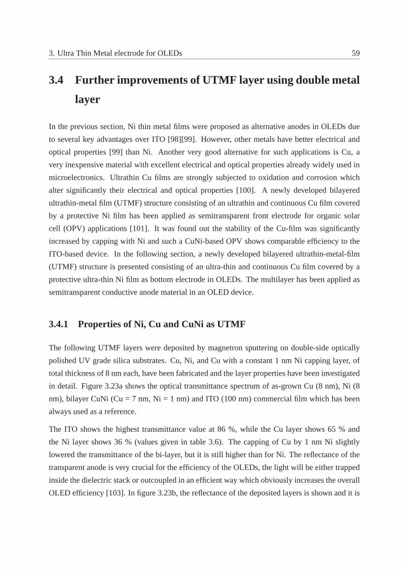
3. Ultra Thin Metal electrode for OLEDs 59
3.4 Further improvements of UTMF layer using double metal
layer
In the previous section, Ni thin metal films were proposed as alternative anodes in OLEDs due
to several key advantages over ITO [98][99]. However, othermetals have better electrical and
optical properties [99] than Ni. Another very good alternative for such applications is Cu, a
very inexpensive material with excellent electrical and optical properties already widely used in
microelectronics. Ultrathin Cu films are strongly subjectedto oxidation and corrosion which
alter significantly their electrical and optical properties [100]. A newly developed bilayered
ultrathin-metal film (UTMF) structure consisting of an ultrathin and continuous Cu film covered
by a protective Ni film has been applied as semitransparent front electrode for organic solar
cell (OPV) applications [101]. It was found out the stability of the Cu-film was significantly
increased by capping with Ni and such a CuNi-based OPV shows comparable efficiency to the
ITO-based device. In the following section, a newly developed bilayered ultrathin-metal-film
(UTMF) structure is presented consisting of an ultra-thin and continuous Cu film covered by a
protective ultra-thin Ni film as bottom electrode in OLEDs. The multilayer has been applied as
semitransparent conductive anode material in an OLED device.
3.4.1 Properties of Ni, Cu and CuNi as UTMF
The following UTMF layers were deposited by magnetron sputtering on double-side optically
polished UV grade silica substrates. Cu, Ni, and Cu with a constant 1 nm Ni capping layer, of
total thickness of 8 nm each, have been fabricated and the layer properties have been investigated
in detail. Figure 3.23a shows the optical transmittance spectrum of as-grown Cu (8 nm), Ni (8
nm), bilayer CuNi (Cu = 7 nm, Ni = 1 nm) and ITO (100 nm) commercialfilm which has been
always used as a reference.
The ITO shows the highest transmittance value at 86 %, while the Cu layer shows 65 % and
the Ni layer shows 36 % (values given in table 3.6). The capping of Cu by 1 nm Ni slightly
lowered the transmittance of the bi-layer, but it is still higher than for Ni. The reflectance of the
transparent anode is very crucial for the efficiency of the OLEDs, the light will be either trapped
inside the dielectric stack or outcoupled in an efficient waywhich obviously increases the overall
OLED efficiency [103]. In figure 3.23b, the reflectance of the deposited layers is shown and it is

3. Ultra Thin Metal electrode for OLEDs 60
visible that the highest reflectance was measured for the Ni layer due to its poor transmittance.
The double layer shows lower reflectance than for the Ni but still higher than for ITO.
350 400 450 500 550 600 650 700 7500
10
20
30
40
50
60
70
80
90
100
ITO Ni = 8 nm Cu = 8 nm CuNi = 7 nm +1 nm
Tr
ansm
ittan
ce (%
)
Wavelength (nm)
(a)
350 400 450 500 550 600 650 700 7500
10
20
30
40
50 ITO Ni = 8 nm Cu = 8 nm CuNi = 7 nm + 1 nm
Ref
lect
ance
(%)
Wavelength (nm)
(b)
Figure 3.23: Transmittance (a) and reflectance (b) over the full visible wavelength range
For the sheet resistance, both ITO and Cu layers show a low value around 15 to 17Ω/sq while Ni
is slightly higher, around 30Ω/sq. It is also observed that the conductivity behavior of the bilayer
UTMF is mainly dominated by the underlying ultra-thin Cu layer [102]. Surface treatment is a

3. Ultra Thin Metal electrode for OLEDs 61
crucial process for the activation of the anode layer, however, an important side effect is the
change of the contact angle [104] for a better spreading of the polymer on the anode surface. A
lower contact angle leads to an uniform layer with an improved anode-polymer contact due to
the change of the surface energy [105], which can be easily proved using the simple but effective
scotch tape test. Several surface treatments have been described and investigated in literature, but
this investigation deals with UV-ozone treatment which seems to be the most efficient one for our
device configuration. It is well known that the ozone treatment affects the hydrophobicity of the
layer by varying the contact angle, and indeed, all the layers including ITO show a reduction of
the contact angle, therefore becoming more hydrophilic, asshown in figure 3.24 as an example
for the CuNi bi-layer.
(a) (b)
Figure 3.24: Contact Angle for CuNi before (a) and after (b) Ozone treatment
A treatment with UV-ozone influences as well the optical and electrical properties. A 10 min
ozone treatment results in an increase of the sheet resistivity of 9 % for Ni, 65 % for Cu, 8.5 % for
Cu-Ni and has almost no influence at all on the ITO layer. Cu layershows a better transmittance
and lower resistivity than Ni. While its transmittance is only 2 % decreased, its sheet resistance
is increased by about 65 % after a 10 min treatment in ozone. Capping the Cu layer with Ni
offers a better stability of the resistivity with ozone exposure, with only an increase of 8 % this
time. The effect of the ozone treatment on the transmittanceis more or less negligible for all the
layers studied.
Looking at the morphology of the various thin layers, the root-mean-square (rms) roughness
measured over an area of 1µm2 of all the layers is quite low (less than 0.7 nm), the rougher layer
being the Cu layer. Surface roughness has to be kept below the thickness of the layer, otherwise

3. Ultra Thin Metal electrode for OLEDs 62
films could be discontinuous and thus non-conductive (figure3.25). A high roughness might also
lead to local short circuits in the device.
(a) (b)
Figure 3.25: AFM pictures from ITO (a) and CuNi (b)
Pre - or postannealing processes are very important for the fabrication of OLEDs. The materials
used in solution processed devices are water-based or contain various solvents. It is well-known
that the presence of solvents or water residues (after the fabrication of the OLEDs) is a limiting
factor for the device lifetime and efficiency. Therefore, annealing processes are crucial for a
functioning device and they might take in a quite broad temperature range with temperatures up
to 200C or even more. The stability improvement of the Cu layer with aNi capping is also
observed upon thermal treatment of the layers, as shown in figure 3.26.
Figure 3.26: Stability of the metallic layers upon thermal treatment (Courtesy of D. S. Ghosh)
The variation of the sheet resistance with thermal treatment reaches high values for temperatures

3. Ultra Thin Metal electrode for OLEDs 63
as low as 100C for the Cu layer, while for the CuNi bilayer, up to 220C the variation in
the sheet resistance is small. Cu films are strongly subjectedto oxidation and corrosion, which
alter significantly their electrical and optical properties. The inevitably partial oxidation of the
Cu layer leads consequently to an increase in the sheet resistance. Ni on the other hand is
characterized by its very slow oxidization rate and protects therefore efficiently the underlying Cu
layer. Aïda Vareaet.al. (Int. J. Electrochem. Sci., 7, p.1288 (2012)) proved that a Ni-rich electro
deposited CuNi film improves the corrosion resistance of the material which is very similar at
surface of the CuNi UMTF bilayer. ITO is known to be stable up tovery high temperatures.
Thus, high temperatures of 300C or more improves the optical and electrical properties of the
ITO. The Ni and the CuNi bilayer also provide a larger work-function, which is beneficial for
the anodic injection. The Haacke figure of meritϕ shows a significant improvement for the
CuNi bi-layer compared to that of the pure Ni even if it still lower than the ITO. The results are
summarized in table 3.6:
ITO Ni 8 nm Cu 8 nm CuNi 8 nm
mean. Transmittance (%) before Ozone 86 36.5 64.1 56.8
mean. Transmittance (%) after Ozone 86 36.8 61.5 58.6
RsΩ/sq before Ozone 16.7 29.6 15.5 15.3
RsΩ/sq after Ozone 16.8 32.4 25.7 16.6
ϕ =T10
AvRS
(after ozone) 13.2 x 10⁻³ 1.4 x 10⁻⁶ 0.3 x 10⁻³ 0.29 x 10⁻³
Contact angle before Ozone 78 63 / 61
Contact angle after Ozone 65 54 / 20
Workfunction (eV) (before Ozone) 5.0 5.1 4.7 5.1
Workfunction (eV) (after Ozone) 5.1 5.2 4.8 5.2
Roughness (nm) (before Ozone) 0.5 0.6 0.7 0.6
Table 3.6: Structural, Optical and Electrical Parameters of the ITO, Ni, Cu and the CuNi layers. The Haacke figure
of merit ϕ was calculated from the average transmittance and the sheetresistance
To summarize, the main drawback of the Cu layer for device application, which is its low stability
to oxidation and temperature, has been alleviated by simplyusing a 1 nm Ni capping layer.
Therefore, the Ni capping makes Cu-Ni UTMF very interesting forthe OLED applications as it
overcomes the stability issue of the Cu layer and increases the work function, still maintaining
good optical and electrical properties.

3. Ultra Thin Metal electrode for OLEDs 64
3.4.2 Double metal layer as anode for bottom light emitting diodes
In the previous section, UTMF anodes were analyzed and applied as semitransparent conductive
anode for bottom light emitting diodes. The following OLED structure has been used in this
investigation with the corresponding layer sequence in figure 3.27.
(a) (b)
Figure 3.27: Schematic of SY-based OLEDs (a) and corresponding band diagram (b) varying the anode material
Figures 3.28a and b compare the current-voltage (I/V) and luminance characteristics of OLEDs
with a thin metal anode against those of a typical ITO anode. It can be seen that the lowest
performance is obtained for the Ni-based device. Slightly higher voltage threshold, lower current
density and lower luminance reflect the poor transmittance and high resistivity of the 8 nm Ni
layer. The luminance of the Ni-based OLED is significant lower although the workfunction
of Ni is similar to the one of ITO and guarantees therefore a similar charge carrier injection.
A limiting factor for the charge carrier transport might be the higher sheet resistance of the Ni
which would explain higher driving voltages but not the lower luminance level. Also the emissive
dipole position is with a simulated value of 56 nm closer to the metallic cathode resulting in a
less efficient radiative recombination due to possible losses at the metal cathode. As a result,
the current efficiency 1.5 cd/A for the Ni-OLED is poor compared to the reference ITO OLED
with 2.9 cd/A. Another limiting factor is the difference of the outcoupling efficiencies of the
different device configuration. The optical interaction inthe stack is explained more in detail
for the presented device structures in the following part ofthe chapter and shows a very low
outcoupling for the Ni-OLED.

3. Ultra Thin Metal electrode for OLEDs 65
0 1 2 3 4 5 6 7 80.0
0.1
0.2
0.3
0.4
0.5
0.6 ITO Ni Cu CuNi
Cur
rent
Den
sity
(A/c
m2 )
Voltage (V)
(a) Current density versus applied voltage
0 1 2 3 4 5 6 7 81
10
100
1000
10000
100000 ITO Ni Cu CuNi
Lum
inan
ce (c
d/m
2 )
Voltage (V)
(b) Luminance versus applied voltage
2 3 4 5 6 7 80.1
1
10 ITO Ni Cu CuNi
Pow
er E
ffici
ency
(lm
/W)
Voltage (V)
(c) Efficiency versus applied voltage
Figure 3.28: IV, LV and efficiency of SY-based OLEDs with the anode being ITO, Ni, Cu or CuNi

3. Ultra Thin Metal electrode for OLEDs 66
The Cu-based device behaves very similarly to the Ni-based device, as the driving voltage at a
given current density is found to be higher than the one of ITO. This difference might be due
to the sheet resistance values of Cu and Ni, which, after the ozone treatment, stand around 32
Ω/sq and 27Ω/sq respectively, compared to 17Ω/sq for ITO. The advantage of the Cu-based
device lies in the higher transmittance of the Cu layer compared to the Ni layer and therefore
it shows a higher luminance level than the Ni-based device. The higher luminance is possibly
obtained due to a shift of the emitter dipole position, simulated to be at 49 nm. When looking at
the device efficiency, the Ni-based and the Cu-based device show a lower efficiency compared to
the ITO-based device.
The CuNi double layer anode has a similar sheet resistance (around 17Ω/sq) to the one of the
ITO resulting in a similar threshold voltage and maximum luminance level for the OLED. A
further increase of the luminance compared to the Ni and Cu-OLEDs has been obtained due
to the lower sheet resistance and the higher transmittance of the CuNi film. The CuNi-OLED
shows a threshold voltage for light emission and a maximum luminance level close to the ITO
reference device. Additionally the emitter dipole position is with a simulated value of 46 nm
well centered leading to an efficient radiative recombination. Furthermore, the current efficiency
has been significantly increased compared to the single layer metal films and is with 2.7 cd/A
close to the value of the ITO-OLED, which again shows the potential of the double metal layer
as anode for bottom light emitting diodes. The results of theOLED measurements including the
calculated power efficiency in lm/W are summarized in table 3.7.
ITO Ni 8 nm Cu 8 nm CuNi 8 nm
VTH / Vmax.Lce (V) 2.4/6.9 2.5/8.6 2.5/11.3 2.4/8.1
max. Luminance (cd/m2) 18730 9265 15024 17165
max. Efficiency (lm/W) 2.1 1.1 1.3 1.9
Table 3.7: Threshold voltage VTH, voltage at maximum brightness Vmax.Lce, efficiency at maximum brightness
efficiencymax.L and maximum efficiency for SY-based OLEDs when using ITO, Ni,Cu or CuNi as anode and CaAg
as cathode.
The difference in terms of OLED efficiency is very likely not only caused by the different elec-
trical properties of the anode metals, but also by the difference in the optical properties within
the OLED structure. An important aspect of metal based OLEDsis the possible presence of
cavity effects, which leads to an angular dependence that isdifferent from that of ITO-based

3. Ultra Thin Metal electrode for OLEDs 67
devices. Hence, the fact that luminous efficiency is comparable in the normal direction does
not necessarily guarantee that it is also in an off-normal direction. Indeed, microcavity OLED
can exhibit significantly enhanced emission in the forward direction as well as a much narrower
emission spectrum [106][107], making evident that possible microcavity effects of the proposed
metal-based devices have to be considered. To this end, the theoretical description of the micro-
cavity effect in OLEDs, as cited in Ref. [107], explains that aweak microcavity effect occurs
associated to the low reflectance of the Cu, Cu-Ni and ITO layers, which is about 15 - 18 % at the
wavelength of the emission peak (for Ni, it is about 30 %). Theelectrically stimulated emission
is slightly shifted for the different material with around 542 nm for the Ni-OLED and around 549
nm for the rest. The highest transmittance and therefore lowest reflectance takes place between
500 and 600 nm for the Cu and CuNi resulting in a low microcavity effect. Furthermore, the
electroluminescence (EL) spectrum for all devices has beenmeasured and the results are shown
in figure 3.29.
500 525 550 575 600 625 650 675 7000.0
0.2
0.4
0.6
0.8
1.0 ITO Ni Cu CuNi
norm
. EL
inte
nsity
(a.u
.)
Wavelength (nm)
Figure 3.29: Electroluminescence spectrum of SY-based OLEDs with the anode being ITO, Ni, Cu or CuNi
The full width half maximum (FWHM) of the spectrum is similar for the Cu, CuNi and for the
ITO-based OLED (around 90 nm). Only the Ni-based device shows a thinner FWHM (around 72
nm), which agrees with the value of its reflectivity – the highest among the three metal electrodes.
The calculated full width at half maximum (FWHM) and the wavelength at the maximum EL
emission have been summarized for the OLEDs in table 3.8.

3. Ultra Thin Metal electrode for OLEDs 68
ITO Ni 8 nm Cu 8 nm CuNi 8 nm
FWHM (nm) 87.3 72.1 91.4 92.2
max. EL (nm) 548.8 542.8 549.2 548.2
Table 3.8: FWHM and the wavelength at the maximum EL emission peak for OLEDs with ITO, Ni, Cu or CuNi as
anode and CaAg as cathode
The electroluminescence and the outcoupling efficiency have been calculated for OLEDs based
on the UTMFs anode and using the measured PL and EL spectrum. The refractive index n and
the extinction coefficient k for the different anode materials (ITO, Ni, Cu, CuNi) and from the
polymer materials used (PEDOT:PSS, SY) have been measured and the results for each material
can be found in the figure section of the appendix. The data have been used in commercially
available optical simulation software.
A shoulder in the EL-spectrum appears for all the measured devices (ITO, Cu, CuNi) at around
600 nm. This shoulder is suppressed for the Ni-OLED and is themain reason for the reduction of
the FWHM. The difference in the EL-spectrum might result fromthe different refractive index
of the Ni and the CuNi as shown in figure A.11 and A13. The change of the spectrum can
be explained in detail when simulating the outcoupled spectrum using the PL spectrum of the
SY (figure 3.30). As an example, the Ni and CuNi OLEDs have been compared since their
FWHM shows a significant difference of 20 nm. The simulated EL spectrum shows a similar
difference at around 600 nm (figure 3.30a). It can be assumed that this effect is only related
to the different optical properties of the stack. The shape of the outcoupled power over the
wavelength is very similar for the Ni and the CuNi (figure 3.30b). But the outcoupled fraction of
the total emitted power is around 1.5 % lower for the Ni deviceover the calculated wavelength
regime. Additionally the curve of the CuNi-bilayer does not follow exactly the Ni curve showing
an enhanced outcoupling between 550 nm and 650 nm which finally results in a difference of
the EL-shape. This effect is more visible when normalizing the outcoupled power between 550
nm and 650 nm (see inset figure 3.30b). This difference of the outcoupling is attributed to the
absorption coefficient, as shown in figure A.11 and A13, whichdrops significantly for the CuNi-
bilayer for wavelengths longer than 550 nm.

3. Ultra Thin Metal electrode for OLEDs 69
500 525 550 575 600 625 650 675 7000.0
0.2
0.4
0.6
0.8
1.0 Ni CuNi
norm
- EL
inte
nsity
(a.u
.)
Wavelength (nm)
(a) simulated EL-spectrum
500 525 550 575 600 625 650 675 7000
1
2
3
4
5
Ni CuNi
Out
coup
led
fract
ion
of to
tal P
ower
(%)
Wavelength (nm)
550 575 600 625 6500.00.20.40.60.81.0
norm
. OC
Wavelength (nm)
(b) calculated out-coupling fraction of total power
Figure 3.30: simulated EL (a), calculated outcoupled fraction of total emitted power (b) for Ni and CuNi OLED
The average outcoupled fraction of the total emitted power by the emitter dipole over the wave-
length range between 500 nm and 700 nm has been calculated forall the device structures.
The highest outcoupled fraction has been calculated for theITO-OLED in this particular de-
vice configuration, resulting in the highest efficiency among the OLEDs. However, the average
outcoupled fraction is not significantly higher for the ITO (4 %) compared to the metal lay-
ers, in particular to the CuNi OLED (3.6 %). Cu, for instance, shows good optical properties
(outcoupled fraction of 3.8 %) with even a slightly higher outcoupled fraction than CuNi which
makes Cu favorable as anode material if it would be thermally stable and not showing such a
fast oxidization. Such values are quite typical for OLEDs with such a configuration indicating
that almost 80 % of the emitted dipole power is therefore lostfor all the presented devices (due
to intrinsic non-radiative losses as explained in the theoretical chapter), but this investigation
also shows the potential of OLEDs when improving the outcoupling. The results show that the
outcoupling intensity as well as the good electrical properties of the CuNi lead to the highest
device efficiency among the UTMF-OLED, even though the efficiency of the ITO-OLED has not
been completely reached. However, the brightness, threshold voltage, as well as the emission
spectrum is very similar which makes CuNi a potential candidate for replacing ITO.
Further improvements in terms of the electron - hole balancewould lead to a further shift of
the emissive dipole position towards the PEDOT:PSS - polymer interface resulting in a further
enhancement of the efficiency for the CuNi OLED. An optimum outcoupling efficiency of around
4.75 (%) can be found for this particular emission spectrum when shifting the emissive dipole at

3. Ultra Thin Metal electrode for OLEDs 70
a position of 21 nm from the PEDOT:PSS - polymer interface. The optimized outcoupled power
as a function of the emission wavelength of the emitting polymer SY and the emitter dipole
position has been simulated in figure 3.31.
Em
itte
r D
ipo
le P
os
itio
n (
nm
)
0.0
7.0
14.0
21.0
28.0
35.0
42.0
49.0
56.0
63.0
70.0
Wavelength (nm)
Figure 3.31: Outcoupled fraction of the total emitted poweras a function of the emitter dipole position with the
distance from the PEDOT:PSS - polymer interface
It is important to point out the role of the capping Ni layer, which has enabled the Cu-Ni layer
to retain good electrical and optical properties after the ozone treatment. This is even more
visible when studying the luminance as a function of the operating time of the devices (shown in
figure 3.32). The graph shows the inital investigation for the lifetime measurement and a deeper
analysis is required to understand the metal anode influenceon the device stability. The lifetime
experiments were performed under inert atmosphere and darkness without encapsulation. The
OLEDs have been stressed for 360 min and the luminance has been measured for every 10 min.
For glass/ ITO device, the luminance decay of the devices is slow, losing around 30 % of its
initial brightness after 360 min. Although the luminance ofthe Cu-Ni anode/ glass substrate
device dropped initially, its decay is very smooth and reaches 35 % after 360 min, at higher
current when compared to the driving current for ITO anode/ glass substrate. Cu anode/glass
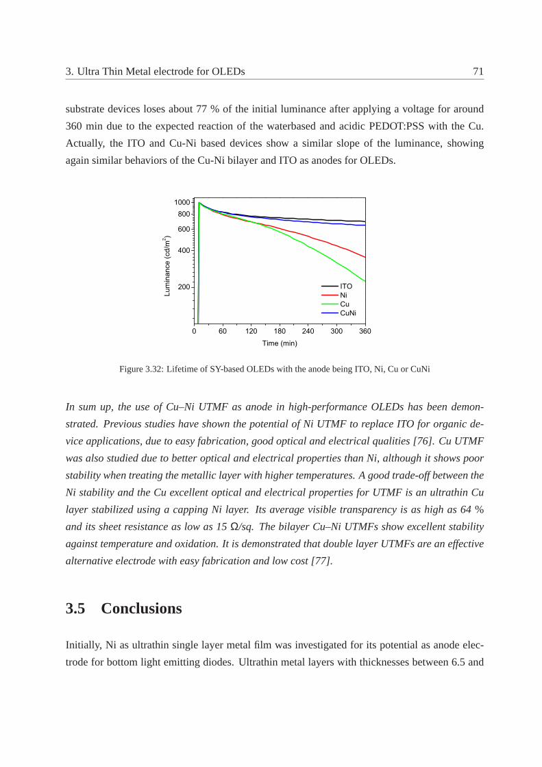
3. Ultra Thin Metal electrode for OLEDs 71
substrate devices loses about 77 % of the initial luminance after applying a voltage for around
360 min due to the expected reaction of the waterbased and acidic PEDOT:PSS with the Cu.
Actually, the ITO and Cu-Ni based devices show a similar slopeof the luminance, showing
again similar behaviors of the Cu-Ni bilayer and ITO as anodesfor OLEDs.
0 60 120 180 240 300 360
200
400
600
8001000
ITO Ni Cu CuNi
Lum
inan
ce (c
d/m
2 )
Time (min)
Figure 3.32: Lifetime of SY-based OLEDs with the anode beingITO, Ni, Cu or CuNi
In sum up, the use of Cu–Ni UTMF as anode in high-performance OLEDs has been demon-
strated. Previous studies have shown the potential of Ni UTMF to replace ITO for organic de-
vice applications, due to easy fabrication, good optical and electrical qualities [76]. Cu UTMF
was also studied due to better optical and electrical properties than Ni, although it shows poor
stability when treating the metallic layer with higher temperatures. A good trade-off between the
Ni stability and the Cu excellent optical and electrical properties for UTMF is an ultrathin Cu
layer stabilized using a capping Ni layer. Its average visible transparency is as high as 64%
and its sheet resistance as low as 15Ω/sq. The bilayer Cu–Ni UTMFs show excellent stability
against temperature and oxidation. It is demonstrated thatdouble layer UTMFs are an effective
alternative electrode with easy fabrication and low cost [77].
3.5 Conclusions
Initially, Ni as ultrathin single layer metal film was investigated for its potential as anode elec-
trode for bottom light emitting diodes. Ultrathin metal layers with thicknesses between 6.5 and

3. Ultra Thin Metal electrode for OLEDs 72
9.5 nm have been investigated and compared with ITO. A 9.5 nm thin Ni film shows a rea-
sonable sheet resistance and workfunction which is suitable for OLED applications. However,
the transmittance is around 33% and therefore much lower than for ITO with 86%. The trans-
mittance of thinner Ni films would be obviously higher, but the drawback is the significantly
increased sheet resistance. Furthermore, the metal film would be discontinuous for thicknesses
below the percolation thickness, which is usually between 3and 6 nm. The Ni film has been
applied as semitransparent conductive anode for bottom emitting OLEDs and it has been shown
that a similar or even higher luminance can be reached even though the transmittance of the Ni
is much lower than for ITO. The improvement is not the result of an improved electrical con-
tact and charge carrier injection, since the power efficiency of the Ni OLEDs is lower due to its
higher driving voltages. The high driving voltage is the result of the missing electron injection
layer leading to an unbalance in electrons and holes. An explanation for the increased luminance
intensity has been found looking at the different optical modes in the device structure. The lu-
minance enhancement is the contribution of an increased outcoupling for the investigated device
specification and the characteristic emission for the used blue-emitting polymer. A simulation
based on the matrix-transfer formalism confirmed this assumption of an increased outcoupling
efficiency. Ni shows therefore its potential as anode electrode with several advantages including
simple deposition, no need for post deposition treatments,and lower cost.
However, the efficiency of the presented OLEDs was still quite poor due to the inefficient electron
injection, which results from the use of only Al on the cathode side. Increasing the overall
efficiency using an electron injection layer (Ca) and PFO and SY as emissive polymer was the
issue in section 3.2.3. The significant enhancement of the luminance as well as the efficiency
is clearly the result of the increased electron injection leading to a more balanced ratio between
electrons and holes. A difference in the electrons - holes ratio influences obviously the position
of the recombination zone. The position of the recombination zone can be simulated and was
shifted from before x = 0.85 (relative distance from the PEDOT - Polymer interface) to 0.26 for
the OLEDs with electron injector and PFO as emissive polymer. The measured efficiencies for
the OLEDs with PFO and Ni were even higher than for the ITO reference OLED with almost a
three-time higher efficiency for the best Ni OLED with a 10 nm thin layer.
To overcome the issues of Ni-metal films such as low transmittance and relatively high sheet
resistance, a double layer based on Cu and Ni has been extensively investigated. Cu shows better
optical and electrical properties than Ni, but poor stability upon heating. Cu as single material

3. Ultra Thin Metal electrode for OLEDs 73
is well-known for oxidizing very fast with a strong negativeimpact on the electrical and optical
properties. It was found that Cu is very stable when capped with a Ni layer, maintaining the
excellent electrical and optical properties of pure Cu and very good stability against temperature
and oxidation of pure Ni. The average transparency in the visible part of the spectrum is around
64 %, which is more than a twofold increase compared to pure Ni. When applied to OLEDs, the
device with CuNi as anode shows the highest efficiencies amongthe metal film based OLEDs.
The efficiency of the CuNi-based OLED is still lower than for ITO in this device configuration;
however, a strong increase has been obtained compared to theNi OLED. A strong enhancement
of the luminance was observed for the double layer with a similar threshold voltage as it was
measured for the ITO. The simulation confirms the significantly increased outcoupling efficiency
for the CuNi-OLED configuration in comparison with the ITO-OLED. The observed temperature
stability, processability at room temperature together with the optical transmittance and electrical
resistivity performances confirm that multilayer Ultrathin Metal Films are serious competitors to
transparent conductive oxides such as ITO.

Chapter 4
Atomic Layer Deposition (ALD) Technique
applied to multilayer organic LEDs
An established method to enhance the efficiency of OLEDs is the use of multilayered device
structures, consisting of layers of organic semiconductormaterials with different energy levels
and functionalities (e.g. charge transport, emission, blocking layers). In small-molecule-based
OLEDs, which are commonly fabricated via vacuum deposition techniques, the fabrication of
heterostructures is relatively straightforward [108][109]. In contrast, in solution-processed
OLEDs, the situation is more complex. When a layer stack is made by solution processing, it
is imperative that a layer is not attacked and dissolved by subsequent coating steps [110][111].
In the past few years many strategies were developed to overcome the dissolution problem and
to prepare multilayer OLEDs by spin coating [112]-[114]. This can be achieved, for example,
by using orthogonal solvents for each layer or by making the deposited film insoluble by, for
instance, a subsequent cross-linking step [114]. Since cross-linking steps require high tempera-
tures and may lead to unwanted diffusion of material, a fully solution processed OLED with good
performance is very difficult to obtain. Recently, a liquid buffer method which completely pre-
vents the dissolution between solution-processed polymer layers was reported to achieve high-
efficiency and stable OLEDs [115].
A possible approach for obtaining multilayer OLEDs is the use of a thin film of a metal-oxide
deposited directly on top of the solution processed organiclayer. C.-Y. Chang et. al. [116] have
shown that OLEDs can withstand an aggressive photolithographic patterning process without
74

4. Atomic Layer Deposition (ALD) Technique applied to multilayer organic LEDs 75
any degradation of the organic layer by using a thin (1 nm) atomic-layer-deposited Al2O3 film
as a protecting layer for the electroluminescent (EL) organic material. A possible routine for the
alignment of the charge carrier transport has been shown in [117] where a 1 nm thin natural
grown aluminum oxide has been used as buffer layer in organic photovoltaic cells. Such Al2O3
can be deposited well controlled via atomic layer depositionas referenced before.
In this chapter, atomic layer deposition (ALD) was used to form Al2O3 films as buffer layers,
taking advantage of ALD’s low defect density, high conformity, and low deposition temperatures
to maximize the surface coverage of such thin films and to avoid thermally degrading the EL
layer. Multilayer OLED structures are realized using sequential solution processing and a thin
Al2O3 film as an intermediate protection layer. Even though ALD is originally a vacuum based
process, there are recent approaches for ALD at atmosphericpressure and R2R manufacturing.
Very recently, BENEQ sold a R2R ALD equipment to the CPI’s NETPark facilities in Sedgefield
in North East England for the development of flexible thin moisture barriers films.
4.1 Experimental details
The same ITO substrate, surface treatments and PEDOT:PSS deposition recipe as described in
chapter 3 have been used for the OLED fabrication. The samples spin-coated with poly(para-
phenylene vinylene) (PPV) copolymer SY were additionally heated for 10 min at 120C due to
the higher boiling point of Toluene (111C) while the samples with 2-methoxy-5-(2-ethylhexyloxy)-
p-phenylene vinylene, namely MEH-PPV were heated for 10 minat 70 C due to the lower
boiling point of chloroform (62C) and low glass transition temperature of the MEH-PPV. The
process recipes are summarized in table 4.1.
Polymer Concentration (mg/ml) Solvent Spincoating Recipe Thickness (nm)
MEH-PPV 10 CHCl3 1500 RPM for 20s 120
SY 5 Toluene 2500 RPM for 20s 80
Alq3−−1 1 CHCl3 2500 RPM for 20s 5 ∗
Alq3−−3 3 CHCl3 2500 RPM for 20s 8 ∗
Alq3−−6 6 CHCl3 2500 RPM for 20s 10 ∗
Table 4.1: Polymer solution concentration, spin-coating recipe and resulting thickness; (∗) indicates that the layers
were measured on glass

4. Atomic Layer Deposition (ALD) Technique applied to multilayer organic LEDs 76
Alq3 (Sigma Aldrich) has been dissolved in chloroform CHCl3 in different concentrations and
spin coated either directly onto the SY film or onto the SY layer protected by the oxide. Al2O3
layers with different thicknesses and deposited at different temperatures have been used in this
chapter. The final multilayer device structure is shown in figure 4.1b.
Figure 4.1: reference OLED (left) and investigated multilayer device with a solution processed Alq3 layer, SY has
been protected by a thin aluminum oxide Al2O3 layer deposited by ALD (right)
4.2 Effect of the deposition process on the intrinsic properties
of organics
High quality Al2O3 can be deposited by the ALD technique when the temperature and the cycling
time (referring to the chemical reaction) are calibrated well [118][119]. In that term, a densely
packed oxide promotes a better protection against environmental impacts (e.g. oxygen, water and
solvents) when used as encapsulation. Usually, the ALD process requires temperatures higher
than the glass transition temperature (Tg) of the polymer, fulfilling the requirements for process-
ing densely packed oxides. It is therefore important to study the effect of the ALD process on the
polymer for two reasons: first, the temperature effect during the deposition process and, second,
the effect of a chemical reaction of the polymer with the precursors. The well-known soluble SY
with a high Tg of around 180C has been used and compared with MEH-PPV with a low glass
transition temperature of around 75C in the following demonstration (figure 4.2a,b). The ALD
layer was deposited with different thicknesses ranging from 0.2 nm up to 5 nm. The process time
was varied depending on the process temperature and the wanted thickness (number of cycles).

4. Atomic Layer Deposition (ALD) Technique applied to multilayer organic LEDs 77
Samples without an ALD deposited oxide have been chosen as reference.
(a) sample with SY as emissive ma-
terial
(b) sample with MEH-PPV as emis-
sive material
Figure 4.2: Al2O3 deposited on SY (a) and MEH-PPV (b)
It should be mentioned that such ALD process has been shown tohave adverse effects on the
organic layer. C.-Y. Changet. al. [116] have shown that the Al2O3 layer deposition disrupt the
conjugation length of the polymer (MEH-PPV in that case). The affected MEH-PPV became
insulating due to the disrupted conjugation, and thereforethe device characteristics deteriorated
drastically. This polymer chain conjugation disruption has been attributed to the exposure to
trimethylaluminum (TMA) and the use of elevated temperature in the ALD process, which ac-
celerated the permeation of TMA vapors into the organic layer [120]. They determined that the
mechanism of the conjugation disruption happens through electrophilic addition of TMA to the
vinylene C=C groups of MEH-PPV. The significant change in the UV-Vis spectrum (spectrum
shift and weakening of the signal) caused by the ALD Al2O3 layer indicated that the TMA expo-
sure affected not only the top surface but also the bulk of theMEH-PPV layer. In order to reduce
the effect of the ALD deposition on the organic layer, the deposition of the Al2O3 layer should be
performed at low temperatures, even though such a low temperature ALD process takes longer
time. The deposition process in this work was very similar tothe ALD process described by
C.-Y. Changet. al. using a pulse of TMA followed by a pulse of H2O [119].
To check the possible deterioration of the organic layer by the ALD process, the optical prop-
erties of MEH-PPV (low Tg) and SY (high Tg) were studied before and after the Al2O3 layer
deposition at different temperatures (80C, 150C and 235C ). Figure 4.3 demonstrates the
importance of a low temperature Al2O3 deposition (80C ) on 2-methoxy-5-(2-ethylhexyloxy)-
p-phenylene vinylene (MEH-PPV) with a glass transition temperature as low as Tg = 75C . The
intensity of the PL spectrum is significantly decreased, even though a low temperature deposition
process (figure 4.3 left) for the deposition of only a 2 nm thinAl2O3 layer has been used. The

4. Atomic Layer Deposition (ALD) Technique applied to multilayer organic LEDs 78
normalized PL spectrum (figure 4.3 right) shows clearly the influence of the deposition process
on the PL spectrum. The spectrum is slightly red shifted and the emission peaks are different.
The polymer properties might be influenced by two process effects, the required elevated process
temperature for the deposition of aluminum oxide layer and the possible degradation of the poly-
mer due to the ALD precursors. A systematic study of the temperature effect and on the chemical
reaction is addressed in the following investigation. The applicability of the ALD process might
depend therefore on the Tg of the polymer and the chemical stability against the reactants.
500 550 600 650 700 7500
1
2
3
4
5
6
7
8 Reference 2 nm Al2O3 at 80°C
PL
inte
nsity
(a.u
.)
Wavelength (nm)500 550 600 650 700 750
0.0
0.2
0.4
0.6
0.8
1.0 Reference 2 nm Al2O3 at 80°C
norm
. PL
inte
nsity
(a.u
.)
Wavelength (nm)
Figure 4.3: PL spectra (left) and normalized PL spectra (right) for MEH-PPV film capped with a 2 nm Al2O3 layer,
deposited at 80C
The phenylsubstituted poly(para-phenylene vinylene) (PPV) copolymer ("‘superyellow"’ (SY)
from Merck) shows excellent properties with a given Tg of around 175C which should lower
the influence of the process temperature on the polymer properties. No shift of the emission
wavelength has been observed in the PL spectrum when depositing at 80C (figure 4.4a). Often
a temperature treatment below Tg is used in order to remove the residual solvent after film depo-
sition. Such a low temperature treatment often increases the PL efficiency due to the change of
the polymer morphology and its influence on the orientation of dipole moments and the degree
of interchain interactions, resulting in an enhanced intensity which is clearly visible for all the
processes [122]. A maximum PL intensity has been measured for the deposition of a 0.8 nm thin
ALD film. An ALD process for the deposition of an Al2O3 thicker than 0.8 nm leads again to
a slight decrease of the PL intensity. However, no damage of the underlying polymer due to the
heating or the migration and reaction with TMA and/or H2O is expected. A change of the poly-
mer itself due to the process temperature has not been expected since the process temperature is
far below the glass transition temperature of the SY.

4. Atomic Layer Deposition (ALD) Technique applied to multilayer organic LEDs 79
500 525 550 575 600 625 650 675 700 7250
500
1000
1500
2000
2500
3000
3500
4000 Reference 0.4 nm 0.8 nm 2 nm 5 nm
PL
inte
nsity
(a.u
.)
Wavelength (nm)
(a) PL spectra of SY after the ALD process at 80C
500 525 550 575 600 625 650 675 700 7250
500
1000
1500
2000
2500
3000
3500 Reference 0.4 nm 0.8 nm 2 nm 5 nm
PL
inte
nsity
(a.u
.)
Wavelength (nm)
(b) PL spectra of SY after the ALD process at 150C
500 525 550 575 600 625 650 675 700 7250
500
1000
1500
2000
2500
3000
3500
4000 Reference 0.4 nm 0.8 nm
PL
inte
nsity
(a.u
.)
Wavelength (nm)
(c) PL spectra of SY after the ALD process at 235C
Figure 4.4: PL spectrum of Al2O3 covered SY, the temperature of the ALD deposition was variedbetween 80C
(a), 150C (b) and 235C (c) and the thickness of the ALD layer was varied between 0.4nm and 5 nm

4. Atomic Layer Deposition (ALD) Technique applied to multilayer organic LEDs 80
It is different for a process temperature of 150C in figure 4.4b, which is close to the glass tran-
sition temperature of the SY polymer. The spectrum for the reference sample and the samples
with a 0.4 nm and 0.8 nm ALD films are identical without any spectral shift or influence on the
PL intensity. For ALD processes with thickness of 2 nm and more, the PL intensity decreases
drastically and the PL emission looks slightly different regarding the shoulder at 600 nm. The
peak at 560 nm and the shoulder at 600 nm are not clearly visible anymore and the PL spectrum
becomes broad and unstructured. It is unlikely that the elevated process temperature decreases
significantly the PL efficiency. Therefore the decrease can be very likely attributed to a chem-
ical reaction of the ALD precursors with the polymer, which on the other hand, is a thermally
activated process [120].
The maximum deposition temperature was considered to be 235C for obtaining a high quality
Al2O3 layer (figure 4.4c). An expected drastic change of the PL spectrum has been observed
for a high deposition temperature of 235C due to the ALD reactants and a process temperature
which is significantly higher than Tg of the polymer. The PL intensity decreases significantly
even when depositing very thin ALD film of only 0.4 nm. No spectrum could be recorded for an
oxide layer thicker than 0.8 nm which corroborates again thedegradation of the polymer itself
due to the thermally activated stronger chemical reaction.
500 525 550 575 600 625 650 675 7000
50
100
150
200
250
300
350 Reference SY_80°C SY_150°C SY_235°C
PL
inte
nsity
(a.u
.)
Wavelength (nm)
Figure 4.5: PL spectrum of temperature treated SY, the temperature of the ALD deposition was varied between 80C , 150C and 235C and with an identical annealing time as for the 2 nm ALD deposition process

4. Atomic Layer Deposition (ALD) Technique applied to multilayer organic LEDs 81
In order to verify if the change of the PL emission spectrum comes purely from the heating
effect or from the chemical reaction of the TMA with the polymer, SY has been spin-coated on
a glass again and treated at 80C, 150C and 235C without the deposition of Al2O3. The
annealing time at different temperatures is equal to the ALDprocess time, so that the effect of
the temperature could be evaluated (figure 4.5). The PL spectrum of the SY does not show a
wavelength shift after the temperature treatment. Only a small decrease of the PL intensity has
been measured for temperature as high as 235C .
Both measurements (figure 4.4 and 4.5) together show that the diffusion of TMA into the poly-
mer layer is stronger for higher temperatures and causes a strong degradation of the polymer
properties. An additional decrease can be expected for a process temperature higher than Tg due
to the morphological change of the polymer. Therefore, a process temperature lower than Tg
should be chosen for the deposition of the Al2O3 in order not to damage the polymer due to the
temperature and moreover the chemical reaction. The ALD-processed SY films show identical
PL spectra at low deposition temperatures due to a low permeation of TMA vapors into the or-
ganic layer. M. D. Groneret. al. [121] have studied the effect of the low temperature on the
quality of the ALD layer grown and have shown that many of the properties of the low tem-
perature Al2O3 ALD films were comparable with the properties of the Al2O3 ALD films grown
at higher temperatures of 177C . Good thin film properties were observed despite decreasing
densities and increasing hydrogen concentrations and impurities. As a result, the ALD process
of Al2O3 deposition should not be detrimental to the SY layer used in this work, and therefore
the protection mechanism of low temperature processed Al2O3 ALD films is investigated in the
next section.
Atomic Force Microscopy was also used to study the heating effect on the morphology of the
polymer film (figure 4.6). The untreated SY film shows the highest roughness (area RMS around
2.5 nm) which decreases with higher temperatures, with 1.7 nm after a temperature treatment of
80 C, 1.1 nm at 150C and with the lowest RMS roughness of 1.0 nm at 235C. It is clearly
visible that a temperature treatment above Tg changes the morphology of the polymer film.

4. Atomic Layer Deposition (ALD) Technique applied to multilayer organic LEDs 82
(a) (b)
(c) (d)
Figure 4.6: AFM images from spin-coated SY-films without annealing (a), annealed at 80C (b), 150C (c) and
235C (d)
The AFM images shown in figure 4.7 illustrate a good uniformity of the ALD film with a thick-
ness of 2 nm and 5 nm all over the organic layer. Furthermore, the organic layer has a root-mean
square (RMS) roughness of around 2.5 nm (figure 4.6a) without any temperature treatment,
which decreases to 0.6 nm (figure 4.7b) when a thin ALD layer (2and 5 nm) is deposited on
top of it. Such parameters should be beneficial for device application in terms of the protection
but, on the contrary, a 5 nm Al2O3 is not suitable, as Al2O3 is an electrical insulator [123].
(a) (b)
Figure 4.7: 2 nm (a) and 5 nm (b) Al2O3 on SY film
An Al2O3 film deposited at 80C with a thickness of 2 nm has been chosen. In the first appli-

4. Atomic Layer Deposition (ALD) Technique applied to multilayer organic LEDs 83
cation, the charge blocking characteristic of the Al2O3 layer is demonstrated with an example
in the next figures before applying the film into the multilayer OLEDs. The insulation Al2O3
has to be thin enough to guarantee a charge carrier transport. It has been demonstrated that the
breakdown electric field for the bulk aluminum oxide is around 10 MV/cm [124]. The charge
carrier transport is dominated by direct charge carrier tunneling for a film thickness of up to 3
nm. Choosing a 2 nm layer thin aluminum oxide guarantees therefore a sufficient charge carrier
transport and protection mechanism. Moreover, this experiment proves if the ALD deposition
process at low temperature has an influence on the emission spectrum due to the migration of the
TMA into the polymer layer. The device structure and the proposed band diagram are shown in
figure 4.8.
(a) (b)
Figure 4.8: OLED device structure (a) with Al2O3 and proposed band diagram (b)
The current density-voltage and luminance-voltage characteristic are presented in figure 4.9a.
As already indicated, the current density is lowered due to the presence of the oxide layer which
acts as charge blocker. As a result, the brightness of the OLED decreases significantly and
its maximum is shifted towards higher voltages. The loweredbrightness and the voltage shift
have a significant influence on the OLED efficiency, shown in figure 4.9b. The voltage drop of
around 0.5 V in the current - voltage behavior is due to the presence of the 2 nm aluminum oxide
film. An applied electric field of around 25 MV/cm can be calculated which is even higher than
the breakdown electrical field given in literature and therefore sufficient high for charge carrier
transport.

4. Atomic Layer Deposition (ALD) Technique applied to multilayer organic LEDs 84
0 1 2 3 4 5 6 7 8 9 100.0
0.1
0.2
0.3
0.4
0.5
0.6
0.7 Reference 2 nm ALD
Cur
rent
Den
sity
(A/c
m2 )
Voltage (V)
1
10
100
1000
10000
100000
Luminance (cd/m
2)
(a) Current Density-Voltage and Luminance-Voltage be-
havior
2 3 4 5 6 7 8 9 100.01
0.1
1
10
Reference 2 nm ALD
Pow
er E
ffici
ency
(lm
/W)
Voltage (V)
(b) Power efficiency versus applied voltage
500 525 550 575 600 625 650 675 7000.0
0.2
0.4
0.6
0.8
1.0 Reference 2 nm ALD
norm
. EL
inte
nsity
(a.u
.)
Wavelength (nm)
(c) normalized EL spectra taken at 8 V
Figure 4.9: OLED characteristic for OLEDs with and without athin 2 nm Al2O3 layer between SY as emissive
polymer and the CaAg cathode

4. Atomic Layer Deposition (ALD) Technique applied to multilayer organic LEDs 85
More important is the record of the emission spectrum of the OLEDs since it shows if the ALD
process changes the intrinsic properties of the polymer filmor if there is a degradation of the
emissive polymer while depositing Al2O3. When normalizing the EL spectrum of both OLEDs,
shown in figure 4.9c, it can be seen that the presence of the oxide and, moreover, the ALD process
itself have no influence on the emission spectrum in this simple device configuration. The effect
on the OLED is therefore truly related to the blocked charge carrier transfer.The characteristics
of these OLEDs are summarized in table 4.2.
Reference without ALD 2 nm Al2O3
Current Densitymax.L (A/m2) 0.8 0.76
VTH / Vmax.L (V) 2.5/9 3/10
max. Luminance (cd/m2) 13220 6360
max. Efficiency (lm/W) 1.4 0.5
Table 4.2: Performance of SY-based OLEDs with and without a thin 2 nm Al2O3 layer between the emissive polymer
and the CaAg cathode
This section shows the importance of a well-chosen process condition for the ALD process when
depositing Al2O3 on film polymer. A degradation of the polymer takes place due to the migration
and possible reaction of the TMA into the polymer. The pure use of Al2O3 as interfacial layer
would result in a lower OLED efficiency because Al2O3 is an electrical insulator. However, the
solution processed injection layer might compensate such an effect. This will be demonstrated in
the next sections.
4.3 The ALD layer used to avoid intermixing of successive
spin coated organic layers
In this section, an ALD deposited layer of 2 nm of Al2O3 is used as a protective layer for a
polymeric film of poly(phenylenevinylene) co-polymer (SY), which was successively covered
by spin coating of a second organic layer [125]. The result isthe deposition by spin coating
of successive organic layers, separated by an ultra-thin Al2O3 layer, without intermixing of the
successive organic layers due to solvent dissolution.

4. Atomic Layer Deposition (ALD) Technique applied to multilayer organic LEDs 86
4.3.1 Study of the solvent influence on the underlying layer.
To study the surface coverage of the ALD layer on top of SY and to show that no penetration of
the solvent from the top organic layer to the bottom organic layer occurs, the following experi-
ment was done. Various SY layer samples were prepared with a 2nm Al2O3 layer deposited at
80 C on top (figure 4.10).
Figure 4.10: Solvent drop on SY protected by a thin Al2O3 layer
Figure 4.11a shows the photos of the samples prepared, whichpresent a strong yellow coloration
uniform throughout the samples.
Figure 4.11: (a.) SY samples with (left) and without (right)a 2 nm thick Al2O3 layer, showing a strong yellow
coloration. A drop of chloroform was deposited on top of bothSY samples. The dissolution of the SY layer below
is clearly seen, with a transparent area appearing where thetoluene was deposited (b) while for the SY covered by
the 2 nm thick ALD layer, no dissolution area nor defect can beseen to the SY layer (c).

4. Atomic Layer Deposition (ALD) Technique applied to multilayer organic LEDs 87
A small drop of solvent was deposited on the Al2O3 coated SY layer, the solvent used being
chloroform. Chloroform has been used as solvent for the Alq3 electron transport/injection layer.
After drying out, the solvent did not damage the bottom SY layer, which still shows the same
yellow coloration uniformly all over the layer (figure 4.11c). If the SY is not protected by the
Al2O3 layer, the small drop of solvent dissolves immediately the SY layer beneath and results
in a white mark on the sample, where the polymer has been dissolved again, as can be seen in
figure 4.11b [125]. Such visual proof shows very well the protective role of the Al2O3 layer to
the organic layer beneath, with no selectivity regarding the solvent used.
Figure 4.12 shows the effect of the solvents on the PL spectrum for samples with or without a
protection layer. A strong deterioration of the PL spectrumhas been observed for the unprotected
SY layer due to the partial dissolution of the SY-film by the solvent. A very strong decrease has
been observed when depositing CHCl3. Looking at the normalized PL spectrum (figure 4.12b),
a strong shift of around 14 nm has been measured.
500 525 550 575 600 625 650 675 7000
100
200
300
400
500 Reference Chloroform 2nm ALD + Chloroform 5nm ALD + Chloroform
PL
inte
nsity
(a.u
.)
Wavelength (nm)
(a)
500 525 550 575 600 625 650 675 7000.0
0.2
0.4
0.6
0.8
1.0 Reference Chloroform 2nm ALD + Chloroform 5nm ALD + Chloroform
norm
. PL
inte
nsity
(a.u
.)
Wavelength (nm)
(b)
Figure 4.12: PL spectrum of SY samples after depositing chloroform and using a 2 nm/ 5nm thin ALD layer as
protection, PL spectrum (a) and normalized PL spectrum (b)
SY SY + CHCl3 SY + 2 nm Al2O3 + CHCl3 SY + 5 nm Al2O3 + CHCl3
FWHM (nm) 80 77.5 76 77.5
max. PL (nm) 557 549 550 552.5
Table 4.3: FWHM and the wavelength at the maximum PL emission for the reference SY film, SY treated with
CHCl3 and protected with a 2 nm and 5 nm Al2O3

4. Atomic Layer Deposition (ALD) Technique applied to multilayer organic LEDs 88
A thin 2 nm Al2O3 layer provides already a protection against solvents. However, the protection
is only lowering the impact of the solvents, since a partial penetration of the solvents into the
polymer cannot be avoided [119][126]. The PL enhancement when depositing a 5 nm film is
the result of the temperature effect at 80C, which has been already observed in the previous
section. The shape of the emission spectrum is similar for all samples, however, a small shift
of the emission spectrum of 7 nm has been still observed due toa partial dissolution of the
polymer surface (figure 4.12b). A 5 nm thick oxide layer provides obviously a stronger protection
resulting in a decreased spectral shift of only 4.5 nm.
In both cases, the emission intensity was higher using a thicker Al2O3 layer resulting in a more
efficient protection. No shift of the emission spectrum was observed and the emission maximum
stays at the same wavelength [127]. Even though it is evident,that a more efficient protection
of the organic layer against solvents is provided by thickerAl2O3 layers, it has to be noted
that Al2O3 is an electrical insulator. Thus, for the multilayer OLEDs,a 2 nm thin Al2O3 is
deposited as protection layer in the following subchapter providing sufficient protection, but still
not blocking all the charges.
4.3.2 Application to multilayer OLEDs; avoidance of intermixing of the
layers
Most of the standard OLED polymers favor hole-transport leading to a charge carrier unbalance
in the device, which results in poor efficiencies. The standard approach to improve the efficiency
of OLEDs is to insert an electron transport and/or injectionlayer (ETL) at the cathode interface
in order to improve the electron transport and/or injection. Such EIL/ETL may consist of an
organic molecule, which is thermally evaporated, or bariumor calcium, which are highly reactive
materials. In this chapter, the possibility to use a spin coated thin film of tris(8-hydroxyquinoline)
aluminum (Alq3) as ETL is investigated by using a thin 2 nm Al2O3 deposited between the two
spin coated layers. Alq3 blocks efficiently the holes due to its deep HOMO level and it is also
a good electron transport layer, commonly used in small molecule OLEDs [128]. Using Alq3
as interfacial layer should therefore provide an improved balance between electron and holes,
leading to a shift of the recombination zone towards the polymer center instead of being close
to the cathode [129]. Alq3 has been spin-coated without any protection onto the polymer film
(figure 4.13b). Furthermore, a Al2O3 layer within the OLED has been prepared (figure 4.13c)

4. Atomic Layer Deposition (ALD) Technique applied to multilayer organic LEDs 89
and, as the final device, an OLED with the complete stack of SY,Al2O3 and Alq3 has been
investigated (figure 4.13d).
(a) (b)
(c) (d)
Figure 4.13: (a) OLED structure without ALD and without electron injection layer as reference, (b) with Alq3
injection layer and without ALD protection layer, (c) with Al2O3 as protection layer and without an electron injection
layer, (d) solution processed Alq3 electron injection layer on a Al2O3 protected SY polymer film
The band diagram is schematically shown in figure 4.14. Figure 4.14a shows the simple OLED
structure without having any interfacial layer for an increased electron injection and transport.
The energy bandgap between the LUMO level of the polymer and the workfunction of the Ag
cathode is big, resulting in a poor electron injection. A different behavior can be expected when
looking at the band diagram in figure 4.14b after inserting Alq3 as electron injection material.
The energetic step between the fermi-level of Ag and the LUMOof Alq3 is slightly smaller than
that to the LUMO of SY. The Alq3 does not only improve the electron transport towards the
emissive polymer, additional it will also improve the poor electron injection. Furthermore, the
holes are blocked at the polymer/ALD/Alq3 interface due to the Alq3’s deep HOMO level.

4. Atomic Layer Deposition (ALD) Technique applied to multilayer organic LEDs 90
(a) (b)
Figure 4.14: proposed band diagram for the reference OLED (a) and the improved OLED with Al2O3 as protection
layer and Alq3 as electron transport layer (b))
The measured current and luminance behavior is shown in the figures 4.15a and b. Additionally,
the power efficiency of these OLEDs has been calculated in figure 4.15c. The OLED efficiency
for the device structure (a) and (c) is poor due to the large energy gap between the cathode and
LUMO level of the polymer. The poor injection of electrons in(a) is even more hindered by
adding an ALD deposited oxide between the polymer and the cathode in (c). Al2O3 blocks ef-
ficiently the charge transport even for very thin layers. Therefore, the efficiency in (c) is even
lower than in (a) due to the higher required voltages and the lower luminance. However, intro-
ducing an electron injection layer (for instance, Alq3) does not necessarily mean that the OLED
efficiency will increase; this can be seen for the OLED (b). The solution processed Alq3 layer
was spin-coated onto the polymer film. The SY film was therefore partially dissolved by the
Alq3 film, as already demonstrated in figure 4.11b. The efficiency of this OLED is very low,
with additionally a strong increase of the threshold voltage for the light emission. It can be seen
that the device performance is significantly improved when inserting a 2 nm thin Al2O3 layer be-
tween the SY and the Alq3 layer (d). Not only does the current density decrease, but additionally
the luminance level is significantly increased leading to anefficiency enhancement of one order
of magnitude (figure 4.15c) from 0.016 lm/W for the referencedevice up to 0.17 lm/W for the
multilayer OLED. When electrically excited, the maximal luminance of 243 cd/m2 measured at
9.7 V for the reference (a) increases up 1445 cd/m2 at the same voltage and with a maximum
possible luminance of 4734 cd/m2 at 12.1 V for the multilayer OLED (d).
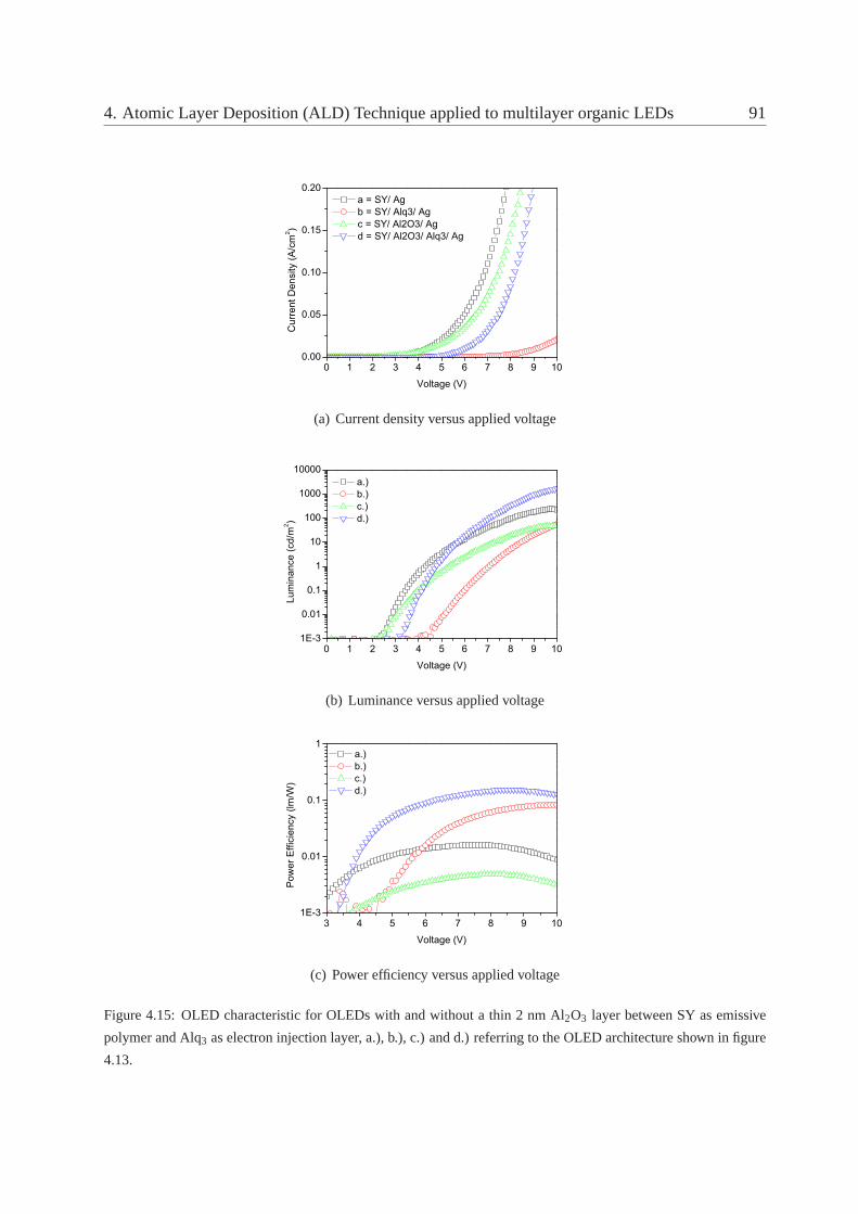
4. Atomic Layer Deposition (ALD) Technique applied to multilayer organic LEDs 91
0 1 2 3 4 5 6 7 8 9 100.00
0.05
0.10
0.15
0.20 a = SY/ Ag b = SY/ Alq3/ Ag c = SY/ Al2O3/ Ag d = SY/ Al2O3/ Alq3/ Ag
Cur
rent
Den
sity
(A/c
m2 )
Voltage (V)
(a) Current density versus applied voltage
0 1 2 3 4 5 6 7 8 9 101E-3
0.01
0.1
1
10
100
1000
10000 a.) b.) c.) d.)
Lum
inan
ce (c
d/m
2 )
Voltage (V)
(b) Luminance versus applied voltage
3 4 5 6 7 8 9 101E-3
0.01
0.1
1 a.) b.) c.) d.)
Pow
er E
ffici
ency
(lm
/W)
Voltage (V)
(c) Power efficiency versus applied voltage
Figure 4.15: OLED characteristic for OLEDs with and withouta thin 2 nm Al2O3 layer between SY as emissive
polymer and Alq3 as electron injection layer, a.), b.), c.) and d.) referringto the OLED architecture shown in figure
4.13.

4. Atomic Layer Deposition (ALD) Technique applied to multilayer organic LEDs 92
The underlying SY-polymer film has been therefore successfully protected by a 2 nm thin Al2O3
film so that a solution processed Alq3 could be deposited on top leading to a significant effi-
ciency increase of the OLED. A decrease of the luminance after reaching its maximum has been
observed and it has been explained literature by the interfacial charge accumulation [130]. This
is more likely the case when the thickness of the layers is notoptimized or when the energy levels
are not optimally aligned.
Additionally, the EL spectra have been measured in order to test if the additional layers (ALD +
Alq3) have an impact on the emission spectrum (figure 4.16). Thereis no shift of the emission
wavelength and no additional emission comes from the Alq3 in the lower wavelength range. The
slight increase at around 600 nm might be a contribution of the additional layers on the optical
properties of the stack.
500 525 550 575 600 625 650 675 7000.0
0.2
0.4
0.6
0.8
1.0 a = SY/ Ag d = SY/ Al2O3/ Alq3/ Ag
norm
. EL
inte
nsity
(a.u
.)
Wavelength (nm)
(a)
500 525 550 575 600 625 650 675 7000.0
0.2
0.4
0.6
0.8
1.0 a = SY/ Ag d = SY/ Al2O3/ Alq3/ Ag
sim
ulat
ed n
orm
. EL
inte
nsity
(a.u
.)
Wavelength (nm)
(b)
Figure 4.16: measured (a) and simulated (b) electroluminescence spectrum for the reference OLED and the OLED
structure using Al2O3 as interfacial layer, a.)and d.) referring to the OLED architecture shown in figure 4.13.
The optical simulation corroborates the above assumption.A measured photoluminescence
quantum yield for the spin-coated superyellow polymer film of 22.5 % has been considered for
the simulation. The optical constants for each material canbe found in the appendix. The out-
coupled EL spectrum has been simulated using the device parameters (thickness of each layer)
as well as the measured photoluminescence spectrum of the SY-film. The developing of the
shoulder between 550 nm and 650 nm on the spectrum of the multilayer film is therefore purely
related to the introduced Alq3 layer with its specific optical constants (figure A.5) as the simu-
lation proved. Additionally, conclusions on the electronic properties of the device stack when
introducing Alq3 can be drawn using the simulated EL spectrum. The relative dipole position

4. Atomic Layer Deposition (ALD) Technique applied to multilayer organic LEDs 93
(relative distance from the PEDOT:PSS - polymer interface)can be calculated using the simula-
tion software. For the device structure shown in figure 4.13a, a relative dipole position of around
0.95 (corresponds to 76 nm distance from the PEDOT:PSS - polymer interface) has been calcu-
lated, while the relative dipole position was clearly shifted towards the PEDOT-Polymer interface
with a value of 0.28 (corresponds to 22 nm distance from the PEDOT:PSS - polymer interface)
for the multilayer device in figure 4.13d. Therefore the inefficient recombination mechanism
close the metallic cathode (in terms of radiation) has been lowered due to the presence of the
Alq3. A dipole position close to the metallic electrode leads to acoupling to surface plasmon
polaritons (SPP).
Additionally, these values have been taken for the calculation of the outcoupling fraction of the
emitted power over the wavelength and as a function of the dipole position (figure 4.17).
500 525 550 575 600 625 650 675 7000
3
6
9
12
15
18 a = SY/ Ag d = SY/ Al2O3/ Alq3/ Ag
Out
coup
ling
fract
ion
of to
tal p
ower
(%)
Wavelength (nm)
500 550 600 650 7000.0
0.2
0.4
0.6
0.8
1.0
norm
. OC
(a.u
.)
Wavelength (nm)
(a)
4 6 8 10 12 14 16 18 207.0
7.2
7.4
7.6
7.8
8.0
outc
oupl
ed fr
actio
n of
tota
l dis
sipa
ted
Pow
er
Alq3 thickness (nm)
(b)
Figure 4.17: Simulated outcoupled power fraction as a function of the wavelength for the reference OLED and the
multilayer OLED (a). Simulated outcoupled power fraction as a function of the Alq3 thickness (b)
The intensity of the optical outcoupling shows a significantdifference between the devices. The
OLED shown in 4.13a has a calculated average outcoupled power fraction of only 2.2 %, which
is significantly lower than 7.7 % for the multilayer OLED. It is therefore very likely that the
multilayer OLED structure not only increases the charge carrier balance, resulting in a recombi-
nation zone shift towards the center, but also it improves the intensity of the outcoupled power.
The outcoupled power is shown as a function of the wavelengthfor both OLEDs. It can be seen
that for the multilayer OLED, the highest outcoupled power fraction of almost 9 % has been
reached at around 590 nm, which is actually exactly the wavelength where a shoulder appears
for this device configuration (see inset 4.17a). The behavior of the outcoupled power for the

4. Atomic Layer Deposition (ALD) Technique applied to multilayer organic LEDs 94
multilayer OLED is shifted towards longer wavelength resulting in a shoulder at around 600 nm
for the electroluminescence spectrum.
Again, the presence of the interfacial layer Al2O3 and the EIL/ETL Alq3 leads to a shift in the
emissive dipole position resulting in an enhancement of theoutcoupled power. The average
outcoupled power varies depending on the thickness of the Alq3 with a maximum of around 7.8
% for an Alq3 thickness of around 8 nm. The intensity of the outcoupled emission varying the
Alq3 thickness and emitter dipole position has been additionally simulated (figure 4.18). The
highest emission intensity (dark red) has been simulated for a dipole position between 16 - 32
nm distance from the PEDOT:PSS - polymer interface and an Alq3 layer thickness lower than 10
nm, which is in an good agreement with the previously presented device structure.
Wavelength (nm)Emitter Dipole Position (nm)
0.0 20.0 40.0 60.0 80.0
Figure 4.18: outcoupled power intensity as a function of theAlq3 thickness and dipole position with the distance
from the PEDOT:PSS - polymer interface
The dipole position has been shifted away from the electrodeas calculated before resulting in a
significant increase of the outcoupling power. The measureddevice characteristics are summa-
rized in table 4.4.

4. Atomic Layer Deposition (ALD) Technique applied to multilayer organic LEDs 95
OLED J(Lmax) (A/m2) VTH / Vmax.Lce (V) Lmax (cd/m2) max. Eff (lm/W)
a.) Reference 0.76 4.3/ 9.7 243 0.016
b.) Alq3 1 mg 0.9 7.1/ 13.8 198 0.08
Alq3 3 mg 0.3 10.6/ 19.4 113 0.07
c.) ALD 0.8 5.3/ 13.6 134 0.005
d.) ALD + Alq3 (5 nm) 0.73 4.8/ 12.1 4734 0.17
ALD + Alq 3 (8 nm) 0.49 5.3/ 13.2 3886 0.19
ALD + Alq 3 (10 nm) 0.12 8.2/ 15.2 701 0.15
Table 4.4: experimental results of SY-based OLEDs with and without a 2 nm Al2O3 layer as protection, varying the
concentration of the spin-coated Alq3 film
The subsequent spin-coating Alq3 layer onto a Al2O3 protected SY polymer film has been suc-
cessfully implemented into the OLED structure. Such a configuration has shown the expected
enhancement in the device efficiency due to the presence of the ETL/EIL. The relative dipole
position was clearly shifted from being very close to the SY -Al2O3 interface towards the SY -
PEDOT:PSS interface as simulated before. Such a shift of theemissive dipole position indicates
an improved charge carrier balance. The result shows the potential of the ALD as protection
and/or interfacial layer. A significant increase of the OLEDefficiency has been measured; how-
ever, the effect has to be investigated for different polymers due to their different required process
conditions (for instance, temperature and used solvents).
As another example, MEH-PPV shows very poor electron conduction. OLEDs with MEH-PPV
as emissive material and without an electron injector hardly emit light. The band diagram as
well as the device structure is shown in figure 4.19. The band diagram shows a big energy gap
between the LUMO level of the MEH-PPV and the workfunction ofthe Al-cathode without an
electron injection layer. The same idea has been applied, asdemonstrated previously. Alq3 was
spin-coated onto the Al2O3 protected MEH-PPV layer and the OLED performance has been
compared with the reference OLED (figure 4.20). Taking into account the low Tg from MEH-
PPV, the impact of the ALD process will be more significant as demonstrated in figure 4.3.

4. Atomic Layer Deposition (ALD) Technique applied to multilayer organic LEDs 96
(a) (b)
Figure 4.19: proposed band diagram for the reference OLED (a) and the improved OLED with Al2O3 as protection
layer and Alq3 as electron injection (b)
The reference OLED shows very poor behavior with a very low efficiency of around 0.002 lm/W.
The maximum luminance of the multilayer OLED is significantly higher with around 900 cd/m2,
resulting in an increase of the power efficiency of around oneorder of magnitude. The efficiency
is still quite low taking into account that the layer thicknesses and process conditions have not
been optimized so far. However, the improvement is quite significant and is related to the shift
of the dipole position away from the Al-cathode due to the introduction of the interfacial Al2O3.
The decrease of the luminance for the MEH-PPV reference OLEDis due to the degradation of the
OLED after reaching its maximum. The results, including thecurrent density at the maximum
brightness, are summarized in table 4.5.
Material MEH-PPV MEH-PPV + ALD + Alq3
Current Densitymax.Lce (A/m2) 0.3 0.68
VTH / Vmax.Lce (V) 4.5/ 7.5 3.5/ 12
max. Luminance (cd/m2) 9 880
max. Efficiency (lm/W) 0.002 0.035
Table 4.5: Performance of MEH-PPV-based OLEDs with and without a thin 2 nm Al2O3 layer between the emissive
polymer and the cathode

4. Atomic Layer Deposition (ALD) Technique applied to multilayer organic LEDs 97
0 1 2 3 4 5 6 7 8 9 10 11 120.0
0.1
0.2
0.3
0.4
0.5 MEH-PPV MEH-PPV_ALD_Alq3
Cur
rent
Den
sity
(A/c
m2 )
Voltage (V)
(a) Current density versus applied voltage
0 1 2 3 4 5 6 7 8 9 10 11 120.1
1
10
100
1000 MEH-PPV MEH-PPV_ALD_Alq3
Lum
inan
ce (c
d/m
2 )
Voltage (V)
(b) Luminance versus applied voltage
3 4 5 6 7 8 9 10 11 121E-4
1E-3
0.01
0.1
MEH-PPV MEH-PPV_ALD_Alq3
Pow
er E
ffici
ency
(lm
/W)
Voltage (V)
(c) Power efficiency versus applied voltage
Figure 4.20: OLED characteristic for OLEDs with and withouta thin 2 nm Al2O3 layer between MEH-PPV as
emissive polymer and Alq3 as electron injection layer

4. Atomic Layer Deposition (ALD) Technique applied to multilayer organic LEDs 98
Both OLED structures show an increase of the efficiency when using Al2O3 as protection layer
and a solution processed Alq3 as electron injection layer. It has been demonstrated that an ALD
deposited Al2O3 film prevents efficiently the degradation of the underlying polymer when spin-
coating a layer on top. Additionally, the charge blocking mechanism of the Al2O3 layer has to
be considered due to its insulation character. Solution processed Alq3 compensates therefore
the charge carrier blocking effect of the ALD film leading to asignificant enhancement of the
luminance and results in a strong increase of the efficiency.Therefore, a good trade-off has to be
found between the protection mechanism and the charge blocking mechanism of the oxide layer.
4.4 Conclusion
In this chapter multi-layered, solution processed OLEDs are developed. Thin intermediate metal-
oxide layer prepared by ALD are used to avoid solvent induceddegradation of the organic layers.
This chapter deals with mainly two issues: 1.) finding the right process condition of the ALD
process for the deposition of oxides onto a polymer layer, and 2.) defining an oxide layer thick-
ness with sufficient protection properties and the charge carrier blocking behavior of the oxide
within the OLED structure. Those ultra-thin ALD films were deposited at low temperatures at
80 C in order to avoid degradation of the bottom organic layer. The degradation of the polymer
results in a change of the PL-spectrum and has been measured for two polymers with different
Tg. It was shown that a 2 nm ALD film on a polymer is very uniform with low roughness. The
deposition process of the Al2O3 at low temperatures onto SY does not degrade the polymer. A
strong degradation of the SY-polymer was found when using higher temperature for the ther-
mally activated chemical reaction during the ALD process. Avery low permeation to various
solvents through the oxide onto the underlying SY-polymer has been demonstrated. Furthermore,
this technique has been applied to the OLED fabrication process, attempting to fabricate both the
emissive layer and the electron transport layer by successive spin coating. No intermixing was
observed between the two organic layers due to the thin ALD film deposited between them. The
device showed an improved luminance and efficiency, which has been expected due to the pres-
ence of the ETL. An enhancement has not been observed when theETL is applied directly on top
of the emissive organic layer. The simulation shows that therecombination zone is shifted away
from the metallic cathode towards the PEDOT:PSS - polymer interface by the presence of the
ALD and Alq3 layer. The additional Al2O3 and Alq3 layers lead to a shift of the emissive dipole

4. Atomic Layer Deposition (ALD) Technique applied to multilayer organic LEDs 99
position away from the polymer-metal cathode resulting in an significant decrease of the non-
radiative losses due to the surface plasmon coupling on the metal cathode surface. Additionally,
the outcoupling intensity is significantly increased leading to a twentyfold increase of the lumi-
nance and a higher efficiency of the OLED of around one order ofmagnitude. The same concept
has been proven using a less efficient polymer, named MEH-PPV. An increase of the efficiency
and brightness in the same order of magnitude has been measured and corroborates the previ-
ously made assumption. Thus, the method reported here improves the applicability of atomic
layer deposition in OLED fabrication and the possibility ofusing solution processed multilayer
for an enhancement of the OLED efficiency.

Chapter 5
Blend of a polymer and an organic small
molecule as emissive layer for OLEDs
A simple approach for the fabrication of efficient OLEDs is the use of blended organic material
in order to avoid multi-layer structures and decrease the complexity of the device architecture.
Many conjugated light emitting polymers are hole conductive showing a low electron mobility.
Low electron mobility leads to an unbalance of electrons andholes in an OLED device structure,
resulting usually in a shift of the position of the recombination zone towards the cathode. The
recombination close to the electrode is known to be inefficient [131]. An increase of the OLED
efficiency can be achieved by doping the polymer with an electron transport material. Both,
the carrier injection and transport can be improved by carefully selecting the materials and their
concentration in the blended polymer [132][133]. Among conjugated polymers, 2-methoxy-5-(2-
ethylhexyloxy)-p-phenylene vinylene (MEH-PPV) has been extensively investigated [134][135]
as host material for polymer blend based devices due to its efficient EL emission and for its hole
transport properties. MEH-PPV as host material was blended with an electron-transport or hole-
blocking material (usually a non-emissive material).It shows a significant enhancement of the
device efficiency when used as emissive layer [132][136]. Forinstance, the device efficiency was
increased by blending MEH-PPV with a newly synthesized electron-transport material (DFD) or
with a hole-blocking material [137][138], but the voltage for the maximum light emission was
shifted towards higher voltages.
In this chapter, MEH-PPV doped with the small molecule electron conductor tris(8-hydroxyquinoline)
100

5. Blend of a polymer and an organic small molecule as emissivelayer for OLEDs 101
aluminum Alq3 was used as active material for the OLED [139]. Both materialsare often used
as emissive layer either for solution processed OLEDs in thecase of MEH-PPV or for vac-
uum processed small molecule OLEDs for Alq3. An efficient energy transfer from the Alq3 to the
MEH-PPV is expected due to the overlap of the emission spectrum of the Alq3 and the absorption
spectrum of the MEH-PPV [140]. The blend has been investigated by means of electrolumines-
cence and fluorescence spectroscopy upon variation of the Alq3 content in the blend. Used in
OLEDs, such a blend shows a significant enhancement for the luminance and power efficiency.
5.1 Experimental details
The OLED fabrication procedure is identical to that described in the previous chapters. The con-
jugated polymer 2-methoxy-5-(2-ethylhexyloxy)-p-phenylene vinylene, namely MEH-PPV, was
blended in different weight concentration with Alq3 (both from Sigma Aldrich) and dissolved
in chloroform CHCl3. The formulations have been stirred overnight and then spincoated on the
PEDOT:PSS layer with no ramp time and 2500 rpm for 30 s. Aluminum (Al) was used as cath-
ode and was thermally evaporated through a shadow mask. The device structure and the finished
device are shown in figure 5.1a,b.
(a) (b)
Figure 5.1: device structure for blend-based OLED (a), working device after fabrication (b)

5. Blend of a polymer and an organic small molecule as emissivelayer for OLEDs 102
5.2 Spectroscopy Study of the Energy transfer mechanism be-
tween the polymer and the organic small molecule
The absorption and emission spectrum for Alq3 and MEH-PPV measured for a thin spin-coated
film are shown in figure 5.2. A strong overlap of the emission spectrum of the Alq3 with absorp-
tion spectrum of the MEH-PPV is indicated with the red hatch.The absorption maximum of the
MEH-PPV was measured to be at 500 nm while the maximum emission wavelength of the Alq3
is at 540 nm.
350 400 450 500 550 600 650 7000.0
0.2
0.4
0.6
0.8
1.0 MEH-PPV Alq3
norm
. ext
inct
ion
(a.u
.)
Wavelength (nm)
0.0
0.2
0.4
0.6
0.8
1.0
norm. P
L intensity (a.u.)
Figure 5.2: optical absorption and photoluminescence for MEH-PPV and Alq3
A broad emission peak can be seen in the photoluminescence spectrum of the MEH-PPV film
with a maximum at 580 nm and a weaker peak at around 620 nm. The features at 580 and 620
nm are assigned to the transition from the lowest vibrational level of the first excited electronic
state to the lowest vibrational level of the ground electronic state (0→ 0) and a combination of its
vibronic replica (0→ 1) and an increasing interchain interaction due to the polymer aggregation
when spin-coated as a film, respectively. This fluorescence signal with its characteristics is the
result of the convolution of the emission of intrachain excitons and interchain species due to the
possible exciton transport along and between the polymer chains. As a result, the usually mea-
sured sharp spectrum with a clear resolution of the vibronicfeatures, as measured for instance
in very low concentrated polymer solution (M. Yan,et.al. Phys. Rev. Lett. 75, p.1992 (1995))
or single MEH-PPV polymer chain, is broadened due to a stronginterchain interaction in the
polymer film [154]. Since interchain interactions lead to the formation of lower-energy excited
(resulting in a redshift) states coupled only weakly to the ground state, they are generally consid-

5. Blend of a polymer and an organic small molecule as emissivelayer for OLEDs 103
ered to lower the luminescence efficiency. An increasing doping concentration might influence
therefore the interchain contribution due to the separation of the polymer chains. This effect
and, as a consequence, resulting influence on the emission spectrum and device performance is
investigated during this chapter.
The optical properties have been measured for MEH-PPV as host material. MEH-PPV was then
blended with Alq3 as electron conductive material in different concentrations (9 %, 17 %, 33 %,
50 % and 60 % weight ratio), spin-coated on glass. The normalized absorption spectrum does
not show any change for the maximum absorption peak, even fora very high blend concentration
(figure 5.3a). The maximum absorption remains located at 500nm for the blended MEH-PPV.
A second absorption peak at 380 nm appears for the blend with an increasing Alq3 amount.
The interaction between two different molecules of the samespecies (MEH-PPV) doped by the
electron transporter Alq3 was investigated by studying the fluorescence measurements. The pre-
sented blended system meets the necessary conditions of Förster-type energy transfer due to the
strong overlap of the donor emission and the absorption spectrum of the acceptor molecule. For
Alq3 concentrations in the range up to 60 %, the blend fluorescenceshows similar spectral fea-
tures as the pure MEH-PPV as it has been demonstrated alreadyin figure 5.2. No substantial
contribution from Alq3 is found when looking at the photoluminescence spectrum of the blend
layer (figure 5.3b). The normalized spectra reveal that the long-wavelength contribution at 620
nm becomes weaker with increasing Alq3 concentration. This may be the result of an increased
separation of individual polymer chains due to the increasing presence of Alq3 molecules and a
resulting reduced chain-chain interaction (figure 5.3c) [141]. A strong aggregation (low separa-
tion of the polymer chains) might, additionally to vibrational feature, lead to an increased num-
ber of weakly emissive species [152]. As the polymer chains become separated by the electron
transporting small molecules, the emission appears to be dominated by single chain MEH-PPV
exciton. No emission coming from the Alq3 is visible for all concentrations.
The FWHM has not been significantly changed when doping the MEH-PPV with Alq3, as shown
in table 5.1. The reference MEH-PPV layer shows a maximum first PL peak at 580 nm with a
calculated FWHM of around 104 nm. These values vary slightly in a range of around 3 nm for
all blend concentrations. It can be therefore concluded that adding Alq3 as electron transport
material in low concentrations does not change significantly the PL spectrum of the host MEH-
PPV material.

5. Blend of a polymer and an organic small molecule as emissivelayer for OLEDs 104
350 375 400 425 450 475 500 525 550 575 6000.0
0.2
0.4
0.6
0.8
1.0 MEH-PPV 9% 17% 33% 50% 60% Alq3
norm
. ext
inct
ion
(a.u
.)
Wavelength (nm)
(a) normalized absorption spectrum MEH-PPV:Alq3
blended films for Alq3 contents from 5% up to 60%.
475 500 525 550 575 600 625 650 675 700 7250
1
2
3
4
5 MEH-PPV 9% 17% 33% 50% 60% Alq3
PL
inte
nsity
(a.u
.)
Wavelength (nm)
(b) CW PL of Alq3 (solid red curve) MEH-PPV (solid
black curve) and the blend for Alq3 contents from 5% up
to 60%.
475 500 525 550 575 600 625 650 675 700 7250.0
0.2
0.4
0.6
0.8
1.0 MEH-PPV 9% 17% 33% 50% 60% Alq3
norm
. PL
inte
nsity
(a.u
.)
Wavelength (nm)
(c) normalized PL spectrum of blended MEH-PPV
Figure 5.3: (a) extinction spectrum, (b) PL spectrum and (c)normalized PL spectrum for MEH-PPV:Alq3 blended
films for Alq3 contents from 5 % up to 60 %.

5. Blend of a polymer and an organic small molecule as emissivelayer for OLEDs 105
MEH-PPV 9 % 17 % 33 % 50 % 60 %
FWHM (nm) 104 101 100 103 110 107
max. PL (nm) 580 574 577 578 583 580
Table 5.1: FWHM and the wavelength at the maximum PL emission intensity for the blended MEH-PPV
A more detailed analysis on the emission contribution is provided by looking at the time-resolved
PL (TRPL). The emission has been detected at the emission maximum of the MEH-PPV at 570
nm. The excitation has been varied between the absorption maxima of the Alq3 (400 nm) or
MEH-PPV (500 nm), respectively. The TRPL shows the influence of the small molecule Alq3
on the luminescence kinetics of the MEH-PPV as emission layer. The blended layer shows
an exponential behavior and the decay function could be fitted by three main components with
their specific percentile contribution. The calculated values for different blend concentrations are
listed in tables B.1 - B.4 in the appendix.
0.0 0.5 1.0 1.5 2.0 2.5 3.0 3.5 4.0 4.5 5.0
0.01
0.1
1 9% 60%
norm
aliz
ed In
tens
ity
Decay (ns)
(a) Excitation wavelength 400 nm, detection
wavelength 570 nm
0.0 0.5 1.0 1.5 2.0 2.5 3.0 3.5 4.0 4.5 5.01E-3
0.01
0.1
1 9% 60%
norm
aliz
ed In
tens
ity
Decay (ns)
(b) Excitation wavelength 500 nm, detection
wavelength 570 nm
Figure 5.4: PL decay for the MEH-PPV emission detected at 570nm and with a blend concentration of 9 % and 60
%, excitation at the absorption maximum of the Alq3 (a), excitation at the absorption maximum of the MEH-PPV
(b)
The PL decay is additionally divided in three different proportions after the exponential fitting
analysis. The tables in the appendix give an overview of the percentage of the PL decay compo-
nent with a certain delay tn. For instance, 63.6 % of the generated photons required 0.15ns for
the decay, 30.9 % of the generated photon required an averagetime of 0.42 ns while only 5.5 %
of the generated photons required an average decay time of 1.1 ns, for pure MEH-PPV and an

5. Blend of a polymer and an organic small molecule as emissivelayer for OLEDs 106
excitation wavelength of 400 nm. Figure 5.4a shows the time-resolved PL decay profiles of the
MEH-PPV fluorescence (probed at 400 nm) of the MEH-PPV:Alq3 blend with a concentration
of 9 % and 60 %. It is clearly visible that the decay time of the blend films are significantly
increased for a concentration of 60 % of Alq3. The time constants of the decay components
increase to maxima of 0.16, 0.47 and 1.98 ns (at 60 % of MEH-PPV:Alq3) compared to 0.14, 0.4
and 1.5 ns for the lower concentration (table B.1). The fluorescence decay kinetics of the blend
is also monitored when exciting MEH-PPV (excitation wavelength 500 nm), as shown in figure
5.4b. The PL decay time is not as significant longer due to the decreased emission contribution
of the Alq3 (excitation wavelength is not at the maximum for exciting the Alq3). The increase
in the photoluminescence lifetime of the MEH-PPV:Alq3 provides further evidence of Förster
energy transfer from the Alq3 to MEH-PPV in the blend films due to the indirect excitation of
the Alq3 in the blend which is an evidence of Förster energy transfer.
Time-resolved spectroscopy evidences the dynamics of excitation transfer from intrachain to in-
terchain species in MEH-PPV and from Alq3 to MEH-PPV for varying Alq3 content (figure 5.5).
The influence of the intrachain and interchain contributionto the blend emission varying Alq3
(percentages 0 %, 9 %, and 60 %) is investigated by carrying out luminescence measurements
with various time windows (i.e. delay intervals) after the excitation.
500 525 550 575 600 625 650 675 7000.0
0.2
0.4
0.6
0.8
1.0
1.2
E MEH-PPV 9% 60% Alq3
norm
aliz
ed T
RP
L in
tens
ity
Wavelength (nm)
E*
(a) excitation pulse with a delay interval be-
tween 0 ps to 960 ps
500 525 550 575 600 625 650 675 700 725 7500.0
0.2
0.4
0.6
0.8
1.0
1.2E E* MEH-PPV
9% 60% Alq3
norm
aliz
ed T
RP
L in
tens
ity
Wavelength (nm)
(b) excitation pulse with a delay interval be-
tween 2.5 ns delay to 17 ns
Figure 5.5: Time resolved PL of MEH-PPV alone (green), MEH-PPV:Alq3 = 9% (blue) and MEH-PPV:Alq3 = 60%
(light blue). The red curve refers to the Alq3 steady state PL emission as a reference. (E) and (E∗) indicate the
double peak signal with the vibrational transitions at 580 and 620 nm.
The delay intervals run from the excitation pulse (0 ps delay) to 960 ps ("‘FAST"’ range) and

5. Blend of a polymer and an organic small molecule as emissivelayer for OLEDs 107
from 2.5 ns delay to 17 ns ("‘MEDIUM"’ range). In the FAST range (figure 5.5a), the fluores-
cence from the three samples with MEH-PPV exhibit similar characteristics (red curves refer to
the CW PL spectrum of Alq3). The signal is dominated by MEH-PPV emission, with the charac-
teristic double peak signal fluorescence transitions visible at 580 nm and 620 nm. The emission
at 620 nm (E∗) loses its intensity with increasing Alq3 content and is therefore related to the
reduced interchain contribution, as pointed out in figure 5.5. As results, a sharper fluorescence
signal has been detected for the highest doping concentration of 60 % with a clear indication of
the vibrational transitions at 580 and 620 nm. The emission from pure MEH-PPV is less struc-
tured and exhibits overlapped interchain and intrachain emission components. The decrease of
the interchain emission component has its origin in the polymer chain separation due to the pres-
ence of the Alq3 molecules. The nature of the emitting species in the blend becomes apparent
when collecting the signal for longer delay times (more appropriate for the Alq3 PL kinetics):
in the case of pure MEH-PPV (figure 5.5b), the intrachain fluorescence rapidly changes into an
unstructured fluorescence centered between 620 nm - 660 nm assigned to MEH-PPV excimers
[142]. In the case of the 9 % and 60 % blend, the emission at longer wavelengths (E∗) is reduced
and tends to dissappear due to the reduced interchain compontribution. Then, the MEH-PPV
excimer formation is nearly completely hindered by the presence of a large amount of Alq3 (60
%). In this latter case, Alq3 emits almost independently from MEH-PPV and its fluorescence
contribution is seen as overlapped by that of MEH-PPV. The observed Alq3 fluorescence com-
ponent lifetime amounts to∼ 6 ns (at 530 nm), i.e., shorter than what is usually measured (τ∼10
ns - 12 ns) at room temperature [143].
It has been shown previously that the intrachain component is not influenced by doping MEH-
PPV with Alq3. The chain – chain interaction is reduced when doping MEH-PPV with Alq3
resulting in a structured fluorescence signal with the characteristic vibrational transitions at 580
and 620 nm and with a lowered emission intensity at 620 nm. Thedifference in the interchain
and intrachain contribution should result also in a difference of the quantum yield which is im-
portant for the use of the blend as emissive layer and this information is additionally required
for the optical simulation (figure 5.6). For the quantum yield measurements in figure 5.6, the
blend layers were excited using either the wavelength at themaximum absorption of the Alq3
(395 nm) or the wavelength at the maximum absorption of the MEH-PPV (480 nm). A de-
crease of the PLQY has been observed for an increasing blend concentration in both cases. This
effect has been observed in various publications. R. Pizzoferratoet.al. (Chemical Physics Let-

5. Blend of a polymer and an organic small molecule as emissivelayer for OLEDs 108
ters 414, p.234, 2005) observed a decrease of the PLQY when blending a PAE co-polymers with
polystyrene or polymethyl-methacrylate since not all the polymer chains within the host polymer
matrix might be effectively dispersed [145] [146]. One explanation has been described as lumi-
nescence quenching mechanism due to low miscibility of the blend components and a possible
dopant aggregation [144]. A possible aggregation at very high Alq3 concentration might result in
locally stronger MEH-PPV interchain interaction due to thelocal compression of the MEH-PPV
polymer chains as a result of the Alq3 aggregates, as described by R. Pizzoferrato. The observed
effect is even stronger for higher doping concentration of the investigated blend where the PLQY
drops from the initial 22 - 24 % (depending on concentration and excitation wavelength) to 18 %
for a blend concentration of 60 %. A lowered PLQY will consequently decrease the outcoupled
power (increasing non-radiative losses) when applying theblend as emissive layer in OLEDs.
0 10 20 30 40 50 60 70 80 90 100
0
5
10
15
20
25
Alq3 excitation (395 nm) MEH-PPV excitation (480 nm)
PLQ
Y (%
)
Blend Ratio (%)
Figure 5.6: Quantum Yield for MEH-PPV:Alq3 blended films for Alq3 contents from 5% up to 60%.
AFM measurements show the morphology difference of the blended polymer reflecting also the
miscibility of the polymer blend (figure 5.7).
(a) (b)
Figure 5.7: AFM images of MEH-PPV:Alq3 blended films with 9 % (a) and 60 % (b) concentration

5. Blend of a polymer and an organic small molecule as emissivelayer for OLEDs 109
The surface roughness is slightly lower for low concentrations (figure 5.7a) and increases for
a high doping concentration of around 60 % (figure 5.7b), which could be an indication of a
possible dopant aggregation due to a lower miscibility at high doping concentrations. A low
surface roughness should be beneficial for device application due to a better interface between
the layers.
To conclude, the modulation observed in the steady state emission spectra of the blends mainly
originates from the different contributions to the fluorescence deriving from excited intrachain
species of MEH-PPV, i.e., excimers states. Progressively passing from low concentrations to
more than 50 % Alq3 in the blend, it is possible to tune the formation of MEH-PPV excimers
(by Alq3 molecules interposition between polymer segments) and, in the limit of Alq3 high con-
centration, to hinder it totally. Whereas the steady state spectrum does not show any evident
contribution of Alq3 fluorescence, by using detection techniques with time resolution and by
properly choosing the delay ranges, it is possible to evidence the contribution of the guest poly-
mer. As a result, as the Alq3 content in the blend increases, the interchain contribution is reduced
with respect to the intrachain one, since the presence of Alq3 molecules augments the distance
between the MEH-PPV chains, progressively hindering the excimer formation. TRPL evidences
the dynamics of excitation transfer from intrachain to interchain species in MEH-PPV and from
Alq3 to MEH-PPV when the Alq3 concentration is increased.
5.3 Performance of the blend as emissive layer for OLEDs
The architecture of the blend-based device was ITO/PEDOT:PSS/Polymer Blend/Al, as seen
in figure 5.8a. The effect on the charge carrier transport wasstudied by the investigation of
the blended MEH-PPV doped with the electron transport smallmolecule Alq3 with different
concentrations as emissive layer in OLEDs. MEH-PPV is a holeconductive material with a
reported mobility between 1 x 10⁻⁵ cm2/Vs and 3 x 10⁻³ cm2/Vs [144]. The electron mobility
is around 1 - 2 order of magnitude lower for MEH-PPV. On the contrary, Alq3 is a typical electron
conductor with good hole-blocking properties due to the lowHOMO energy level of around 5.6
eV and with a maximum electron mobility of around 4 x 10⁻⁵ cm2 [145]. The energy band-
diagram shows the energy level for each layer (figure 5.8b). MEH-PPV is blended with Alq3
in different concentrations which might influence the electronic nature of the blended MEH-
PPV within the OLED structure. Alq3 blocks also efficiently the holes due to its deep HOMO

5. Blend of a polymer and an organic small molecule as emissivelayer for OLEDs 110
level. Therefore, the holes are supposedly trapped at the MEH-PPV:Alq3 interface [146]. The
majority charges are holes traveling form the anode (ITO) towards the Al cathode. The injection
of electrons is very limited due to the energy gap between theworkfunction of the Al and the
LUMO level of the MEH-PPV. On the other hand, the presence of Alq3 might lead to an improved
transport of electrons due to its higher electron mobility.Both effects might lead to a shift of the
emitter dipole position and an increased radiative recombination rate.
(a) (b)
Figure 5.8: OLED architecture for blended OLEDs (a) and proposed band diagram (b)
The electrical characterization of the fabricated OLEDs shows that the current density decreases
when increasing the Alq3 amount (figure 5.9a). On the other hand, an increasing luminance was
measured when doping MEH-PPV with the highest luminance reached for a concentration of
only 9 % of the Alq3 (figure 5.9b). The Alq3 favors the transport of electrons throughout the
blend layer and the blocking of the holes due to the deep HOMO energy level [144][145]. Since
small amounts of Alq3 in the blend do not provide efficient hole blocking, the current flow is still
high. For higher Alq3 concentrations, the overall current density decreases continuously as the
confinement of the holes becomes more efficient due to a denserAlq3 network. As the separation
of the polymer chains by Alq3 insertion becomes larger for very high concentration (resulting
very likely in a dopand aggregation for very high concentrations), the interchain charge transport
is hindered, thus reducing the carrier mobility. Such a behavior is more visible for very high
concentrations of Alq3 due to the rapid decrease of the current density. The threshold voltage
increases significantly for Alq3 content above 33 % weight concentration from originally 5 V up
to 21 V for the highest concentration.

5. Blend of a polymer and an organic small molecule as emissivelayer for OLEDs 111
0 2 4 6 8 10 12 14 160.00
0.02
0.04
0.06
0.08
0.10
MEH-PPV 9% 33% 50%
Cur
rent
Den
sity
(A/c
m2 )
Voltage (V)
(a) Current density versus applied voltage for MEH-
PPV:Alq3 OLEDs
0 2 4 6 8 10 12 14 160.01
0.1
1
10
100
1000
10000 MEH-PPV 9% 33% 50%
Lum
inan
ce (c
d/m
2 )
Voltage (V)
(b) Luminance versus applied voltage characteristic for
MEH-PPV:Alq3 OLEDs
4 6 8 10 12 14 161E-3
0.01
0.1
1 MEH-PPV 9% 33% 50%
Effi
cien
cy (l
m/W
)
Voltage (V)
(c) Power efficiency versus applied voltage characteristic
for MEH-PPV:Alq3 OLEDs
Figure 5.9: characteristic for OLEDs with MEH-PPV:Alq3 as active emissive layer at different concentrations

5. Blend of a polymer and an organic small molecule as emissivelayer for OLEDs 112
The increased presence of electrons and the hole blocking mechanism due to Alq3 might result
in a shift of the emissive dipole towards the center of the polymer and away from the inefficient
recombination close to the metal cathode. The power efficiency in lm/W shows a significant
improvement compared to the reference MEH-PPV device (figure 5.9c), due to the increase
of the luminance by almost keeping the same voltage and current density. The results of the
measurements are summarized in table 5.2.
Weight concentration (%) 0 9 17 33 50 60
Current Densitymax.Lce (A/m2) 0.43 0.42 0.37 0.38 0.22 0.24
VTH / Vmax.Lce (V) 5.5/14.5 5/15.5 4,5/16 5/19 12,5/27 21/40
Luminance (cd/m2) 48 1106 919 709 268 153
max. Efficiency (lm/W) 0.003 0.055 0.05 0.03 0.01 0.005
Table 5.2: Current Density (A/m2) and efficiency (lm/W) at the maximum brightness (cd/m2) for MEH-PPV:Alq3
varying the doping concentration. Best overall performance for the blend OLEDs with a concentration of 9 %
The reference device exhibits a broad EL band centered at around 600 nm, which is assigned to
the convolution of the emission of intrachain excitons and interchain species [142][139] (figure
5.10).
500 525 550 575 600 625 650 675 700 725 7500.00.10.20.30.40.50.60.70.80.91.01.1
MEH-PPV 9% 17% 33% 50% 60%
norm
aliz
ed E
L
Wavelength (nm)
Figure 5.10: Normalized EL spectra for various Alq3 concentrations in the blend as active layer. The arrow shows
the decay of the emission intensity at around 620 nm

5. Blend of a polymer and an organic small molecule as emissivelayer for OLEDs 113
Such a broad structure is especially a characteristic for doping concentrations lower than 33 %
Alq3. Above 33 %, as the Alq3 amount increases, the lower - energy component at around 620
nm of the emission loses intensity and almost disappears, leaving a broadband emission peaked
at 580 nm with a shoulder at 620 nm. The FWHM is reduced from 110 nm for the pure MEH-
PPV OLED up to 55 nm for the highest doping concentration of 60% (table 5.3). The EL
spectra show no Alq3 emission contribution for all blend concentrations [147].A small blueshift
of around 10 nm at the FWHM has been observed for the EL spectrumof the blended layers.
Several publications reported such an effect for blended polymers [148][149]. To clarify, the
blend layers have been processed under the same conditions and using the same solvents. It is
therefore unlikely that the EL shift is related to the process conditions. The changes in the EL
and PL spectrum upon Alq3 doping are often understood in terms of higher sensitivity of the
EL to the chain separation due to the transport of the electrical excited charge carriers, which
happens mainly across the polymer chains [150][151]. However, the lowered emission intensity
at 620 nm as result of the increased Alq3 concentration is not as significant when recording the
CWPL (figure 5.3b) leading to the assumption that the position of the emissive dipole in the
device accounts for the substantial change of the EL spectrum.
MEH-PPV 9 % 17 % 33 % 50 % 60 %
FWHM (nm) 110 110 122 90 67 55
max. EL (nm) 619 606 607 570 571 573
Table 5.3: FWHM and the wavelength at the maximum EL emission peak for blended MEH-PPV OLEDs
The device structure, the CWPL spectrum, the measured EL spectrum, the PLQY and the optical
constants for each layer are required for the simulation of the EL spectrum and the calculation of
the emissive dipole position. The PL and EL spectrum are examined experimental previously in
figure 5.3b and 5.10. The measured transmittance and reflectance required for the calculation of
the optical constants are shown in figure A.14 and A.15. The calculated refractive index n and
the extinction coefficient k for each blend concentration are measured and shown in figure A.4
- A.10. A good agreement between the experimental results (figure 5.10) and simulated outcou-
pled emission spectrum for the pure MEH-PPV and the blend with a concentration of 9 % and
60 % has been found, as shown in figure 5.11a. The shape of the spectra for the given blend
concentrations seems to be similar when comparing the experiment and simulation. The dipole
position has been calculated for the previously simulated blend concentrations (MEH-PPV, 9 %

5. Blend of a polymer and an organic small molecule as emissivelayer for OLEDs 114
and 60 %) (figure 5.11b). The passive optics simulation clearly shows the shift of the emissive
dipole position without consideration of the electronic properties such as charge carrier injection
or charge carrier mobilities. For the undoped MEH-PPV, an emitter dipole position with a dis-
tance of only 5 nm from the metallic cathode - polymer blend interface has been calculated taking
into account an emissive layer thickness of 150 nm. The calculated position of the emitter dipole
was found to be around 26 nm away from the metallic cathode - polymer blend interface for a
concentration of 9 %. More significant is the shift of the emitter dipole for the highest concen-
tration. The emitter dipole position is 125 nm away from the metallic cathode - polymer blend
interface. Again, the simulation is based on passive opticscalculation without consideration of
charge transport and recombination mechanism. As a result,the simulation clearly shows that
the polymer chain separation and its influence on the PL spectrum and PLQY does not influence
significantly the EL spectrum. In fact, the significant decrease at 620 nm is mainly the result of
the shifted emitter dipole position towards the anode side of the active layer.
500 525 550 575 600 625 650 675 700 7250.0
0.2
0.4
0.6
0.8
1.0 MEH-PPV 9% 60%
norm
. sim
ulat
ed E
L (a
.u.)
Wavelength (nm)
(a) (b)
Figure 5.11: simulated EL spectrum for various blend concentration (a), calculated emitter dipole position (b)
Figure 5.12 shows a deeper analysis of the influence of the emitter dipole position and the
changed intrinsic properties on the emission spectrum and their relationship to each other. The
electroluminescence spectrum has been simulated in figure 5.12a using the reference blend
OLED (concentration 9%, black) with n, k, PL and PLQY when doping MEH-PPV with 60
% of Alq3 and keeping the emitter dipole position as calculated for the 9 % blend concentra-
tion (red) and vice - versa (green). A change of the intrinsicproperties of the polymer due to a

5. Blend of a polymer and an organic small molecule as emissivelayer for OLEDs 115
high doping concentration (intrinsic properties) lowers the second peak of the emission spectrum
(red). The second peak at 620 nm is completely suppressed when shifting the emitter dipole
very close to the PEDOT:PSS - polymer interface (as for a doping concentration of 60 %) and
keeping the intrinsic properties (blend concentration 9 %). This simulation proves again that the
difference of the PL and EL spectrum is rather related to the strong shift of the emitter dipole
than to the change of the intrinsic properties.
The emitter dipole position and the intrinsic properties will consequently influence the charac-
teristic of the outcoupled power fraction. Figure 5.12b illustrates the simulation results. The
outcoupling characteristic for the reference blend device(9 %) and the device with the influ-
enced intrinsic properties are very similar, however, the average outcoupled fraction is lowered
from 3.3 % to 2.61 %. A different characteristic of the outcoupled fraction over the wavelength
has been simulated when shifting the emitter dipole towardsthe PEDOT:PSS - polymer interface
(green curve). The average outcoupled power is also loweredto 2.7 % in this particular case.
This drastic change of the outcoupling characteristic whenshifting the emitter dipole is therefore
mainly responsible for the change of the EL spectrum since the outcoupling around 570 nm is
enhanced while the outcoupling at 620 nm is almost completely suppressed.
500 525 550 575 600 625 650 675 700 7250.0
0.2
0.4
0.6
0.8
1.0 Experiment n, k, PL, PLQY 60% Dipole position 60%
norm
aliz
ed E
L (a
.u.)
Wavelength (nm)
(a)
500 525 550 575 600 625 650 675 700 7250
1
2
3
4
5
6 Experiment n, k, PL, PLQY 60% Dipole position 60%
Out
coup
led
fract
ion
of to
tal p
ower
(%)
Wavelength (nm)
(b)
Figure 5.12: simulated EL spectrum (a) and outcoupled fraction of total power (b) for a doping concentration of 9
& varying either the dipole position or the intrinsic properties
An optimization of the optical characteristics of such a device configuration should consider a
low doping concentration since the intrinsic material properties are maintained and the shift of

5. Blend of a polymer and an organic small molecule as emissivelayer for OLEDs 116
the emitter dipole does not influence the EL spectrum and might lower therefore the outcoupling
efficiency. The simulation results are in good agreement with the experimental results when
using a low doped MEH-PPV blend as emissive layer in OLEDs (table 5.2). The outcoupled
fraction of the total emitted power has been simulated for the pure MEH-PPV device, the best
blend device (9 %) and the blend with the highest doping concentration (60 %) (figure 5.13a).
The simulation shows a significant increase of the outcoupled power fraction for the low blend
concentration (up to 3.3 %), while the outcoupled fraction is around 2 % lower for the reference
MEH-PPV and the high concentration blended OLED (figure 5.13a). The outcoupled fraction of
the total power depends on the intrinsic optical propertiesof the blend influenced by the doping
concentration (n, k, PL, PLQY) and moreover the dipole position as previously proved. The
average outcoupled power fraction has been also evaluated for the OLEDs as a function of the
emitter dipole position (figure 5.13b), assuming that the electrical properties will be maintained.
500 525 550 575 600 625 650 675 700 7250
1
2
3
4
5
6 MEH-PPV Blend 9% Blend 60%
Out
coup
led
fract
ion
of to
tal p
ower
(%)
Wavelength (nm)
(a)
0 15 30 45 60 75 90 105 120 135 1500
1
2
3
4
5
6
7
8 MEH-PPV 9 % 60 %
Out
coup
led
fract
ion
of to
tal P
ower
(%)
Dipole position (nm)
(b)
Figure 5.13: outcoupled fraction of total emitted power over the emission wavelength of the blend devices (a),
average outcoupled fraction for blended OLEDs as a functionof the relative dipole position (b) with an indication
of the calculated emitter dipole position for these particular device configurations
The dependence of the outcoupled power on the emitter dipoleposition is clearly visible. The
MEH-PPV and blend 9 % OLED exhibit a very similar characteristic for the outcoupled power
fraction since the low concentration of Alq3 does not influence significantly the intrinsic optical
properties of the MEH-PPV, as seen when evaluating the PLQY (figure 5.6), the PL (figure 5.3)
and EL (figure 5.10) spectrum and the optical constants (figure A.6). The enhancement of the
outcoupled power fraction is therefore mostly related to the shift of the emitter dipole position,

5. Blend of a polymer and an organic small molecule as emissivelayer for OLEDs 117
as shown in figure 5.13b for a low doping concentrations. When doping MEH-PPV with a high
amount of Alq3, the intrinsic material properties, such as n, k, PLQY and the photoluminescence
spectrum are strongly influenced. As a result, the characteristic of the outcoupled power fraction
as a function of the emitter dipole position has been changed(figure 5.13b).
An optical optimization would lead to a significant increaseof the outcoupled power when shift-
ing the emitter dipole towards the center of the blend layer,as illustrated in figure 5.13b (assum-
ing that the electrical performance of the OLED is not affected). An optimum distance of the
emitter dipole of 79.5 nm from the metallic cathode has been calculated reaching a maximum
outcoupling power fraction of 6.76 % (polymer thickness 150nm). Changing the thickness of
the emissive layer also influences the distance of the emitter dipole to the electrodes keeping the
relative position within the polymer. An optimized layer thickness leads to higher outcoupling
power intensities, as shown in figure 5.14., since the distance of the emitter dipole to the metallic
cathode is larger. An optimum for the blend thickness has been found at 380 nm reaching an
outcoupled power fraction of 6.66 %. Again, the optimization method considers only the optical
parameters and does not take into account the electronic properties of this device structure.
100 200 300 400 500 600 7000
1
2
3
4
5
6
7
8
380
Out
coup
led
fract
ion
of to
tal p
ower
(%)
Emitter thickness (nm)
6.66
Figure 5.14: Simulated outcoupled power fraction and its maximum at 380 nm as a function of the thickness of the
blend layer with a concentration of 9 % Alq3.
The best blend OLED device can be compared with the multilayer structure, which has been
investigated in chapter 4.3.2 (figure 4.19). Both concepts presented in this thesis show a strong
improvement compared to the reference OLED. It has been proved that the blending of the host
polymer can even lead to higher efficiencies than multilayerOLEDs when optimizing the doping
concentration. The best blend device shows higher luminance values at much lower current den-

5. Blend of a polymer and an organic small molecule as emissivelayer for OLEDs 118
sities compared to the multilayer OLEDs. The charge carriertransport in such a blend structure
is not hindered due to the presence of an interfacial protection layer. As an advantage, the mul-
tilayer device shows a lower threshold voltage which might be beneficial for some applications.
These both concepts have to be understood as model due to the use of commercially available but
less efficient materials. The choice of solution processed multilayer or blend device concept de-
pends on the required specifications. The measured characteristic of the devices are summarized
for comparison again in table 5.4.
Material MEH-PPV:Alq3 (9 %) MEH-PPV + ALD + Alq3
Current Densitymax.Lce (A/m2) 0.42 0.67
VTH / Vmax.Lce (V) 5/15.5 3.5/ 12
max. Luminance (cd/m2) 1106 880
max. Efficiency (lm/W) 0.055 0.035
Table 5.4: Comparison of MEH-PPV based OLEDs, 1.) MEH-PPV was blended with 9 % Alq3 and 2.) multilayer
device with Al2O3 and Alq3
The significant increase of the MEH-PPV OLED efficiency via doping with Alq3 is the result of
an improved charge carrier transport. An increase of the electron transport can be expected due
to the presence of the electron transport and hole blocking material Alq3. The increased doping
concentration leads to a shift of the emissive dipole position towards the center which prevents
the inefficient and non-radiative recombination close to the metallic electrode. Additionally, the
outcoupled fraction of total power has been increased due to the shift of the emitter dipole. As
a result, a significant enhancement of the OLED luminance fora low doping concentration at
similar voltages and similar current densities has been measured. A significant decrease of the
emission intensity at around 620 nm for increasing Alq3 concentration has been recorded when
examining the EL spectrum. It has been reported that the electroluminescence signal responds
more sensitively to the interchain contribution due to the charge carrier transport across the
polymer chain. However, the difference between the PL and EL signal is very significant and the
passive optics simulation disproved this conclusion. The decreased emission intensity at around
620 nm can be related to the difference in the optical path dueto the shift of the emitter dipole
resulting in an increased outcoupling efficiency. The multilayer concept from chapter 4 has been
compared with the blend OLED, showing slightly lower performances when using multilayer
structures.

5. Blend of a polymer and an organic small molecule as emissivelayer for OLEDs 119
5.4 Conclusion
Blending of polymers is an efficient solution for increasing the efficiency of solution processed
OLED devices. Conjugated polymers are usually hole-conductive and the electron mobility is
very low. The energy transfer from the guest small molecule Alq3 to the host polymer MEH-PPV
has been elaborated in this chapter. Alq3 has been added in different concentrations to MEH-
PPV and the optical and electrical properties have been evaluated. It has been shown that no
contribution of the Alq3 has been measured for the steady state photoluminescence measurement.
TRPL evidences the dynamics of excitation transfer from the intrachain to interchain species in
MEH-PPV and from Alq3 to MEH-PPV when the Alq3 concentration is increased. As the content
of the Alq3 in the blend increases, the interchain contribution to PL isreduced with respect to the
intrachain contribution, since the presence of the Alq3 molecules augments the distance between
the MEH-PPV chains, progressively hindering the excimer formation. The OLED efficiency
has been increased significantly taken into account that no electron-injection has been inserted
between the blend and the Al-cathode. The increase of the luminance when blending MEH-
PPV at similar voltages and current densities can be therefore attributed to the improved electron
transport and the resulting shift emissive dipole away fromthe inefficient recombination position
close to the metallic cathode. However, not only the electronic properties have to be considered in
such a blend device. Blending the host polymer also changes the optical characteristic in terms of
transmittance and reflection. The calculated absorption coefficient k and refractive index n show
strong wavelength dependence and it has been proved that thedoping concentration influences
also the outcoupled emission spectrum. A drastic decrease of the emission intensity at 620 nm
has been measured for the electroluminescence spectrum. A higher response sensitivity of the
EL signal on the interchain contribution has been considered but this explanation is not sufficient
for such a decrease. The simulation proves that the difference of the EL and PL spectrum can
explained by the difference of optical path length due to theshift of the emissive dipole away
from the metallic electrode.Additionally, the outcoupledfraction of the emitted total power by
the emitter dipole is around 2-times as high as for the only MEH-PPV device when doping with
9 %. It is therefore mandatory to consider two effects when blending a polymer: optimizing the
concentration in respect to the desired electronic properties and controlling the influence of the
guest small-molecule on the optical characteristic withinthe OLED stack.
Chapter 6
Summary and Outlook
The introduction of OLEDs for applications such as advertisement or signages is limited due to
the high price of the OLEDs resulting from the use of ITO and the complex and cost intense
processing for achieving high efficient devices. A significant motivation for the applicability
of OLEDs in different niche markets would be a low cost deviceusing commercially available
materials and without ITO and not necessarily achieving high efficiencies and long lifetimes. The
present thesis analyzes different methods for the efficientuse and improvement of commercially
available materials for their application in organic lightemitting diodes. Furthermore, these
materials have been used also in solution processed multilayer OLEDs using an ALD deposited
aluminum oxide film within the stack. The focus of the thesis is to find alternative processes
and material combinations without being focused, in this initial state, on record efficiencies of
OLEDs. Nevertheless, similar or even higher efficiencies have been reached for the proposed
techniques which already show the promising potential of the ideas herein presented even though
further work is required for a deeper analysis.
Three main topics have been covered throughout the thesis. The chapter 3 deals with the re-
placement of ITO using ultra-thin metal films. ITO is one of the cost drivers of OLEDs and it
has also a few fundamental disadvantages due to its couplingability, processing and brittleness
when using flexible substrates. The field of applications of the ALD has been further exploited in
chapter 4. Only a few nanometers thin aluminumoxide layer has been deposited onto the active
emissive polymer to prevent intermixing when spin-coatingan electron transport material on top.
However, intermixing is a desired process when using blendswhere a host material (MEH-PPV)
120

6. Summary and Outlook 121
is controlled doped with an electron transport material (Alq3). The energy transfer and its effect
on the OLED efficiency have been investigated in chapter 5.
It is well know that OLEDs have a poor outcoupling efficiency,which is mostly limited by the
relatively thick conductive and transparent ITO anode. Therefractive index of this oxide is dif-
ferent from the polymer refractive index and influences therefore the intensity of the outcoupling
power. (see equationηout=(1 / 2n2)). Replacing the commonly used ITO as anode material is
one of the main issues in research nowadays. Promising candidates for the replacement of ITO
as electrode materials are ultra-thin metal films (UTMF), such as Ni and a double layer CuNi
layer as presented in chapter 3. Ultra-thin Ni layers can be easily and controlled deposited and
do not require any further treatments. The sheet resistanceand a surface roughness is a bit higher
for the Ni film compare to the ITO. The workfunction matches the HOMO level of the on top
spin-coated PEDOT layer, so that an efficient injection of holes can be guaranteed. The optical
characterization shows that the transmittance is around three times lower. However, an improved
OLED efficiency and a higher brightness can be obtained when applying such an ultrathin Ni
film as anode in OLEDs. The intensity of the outcoupled power is not only dependent on the
transmittance of the layer but also on the thickness due to the possible waveguiding modes. It
has been proved, using a commercial simulation software, that the waveguiding is lowered for
the Ni-film due to its low thickness, which results in an improved outcoupling. Ni has been im-
plemented in OLEDs with different emissive active polymers(SY and PFO). The OLED with Ni
and PFO show even a higher brightness than the ITO based OLED but the efficiency in lm/W is
lower due to the poorer electronic properties of the Ni film and due to the poor electron injection.
Therefore, a further increase of the performance of Ni-based OLEDs requires a further improve-
ment of the material properties itself and an improved electron injection using an interfacial layer
between the polymer and the metal cathode. For instance, pure Cu shows better optical and elec-
trical properties than Ni, but it is not very compatible as pure anode material due to its unstable
behavior within the OLED structure. It was found, however, that these excellent properties can
be maintained capping the Cu layer with Ni forming a CuNi interface which is additionally re-
sistant against oxidization. The transparency is higher than the pure Ni and reaches 64 % for
the visible light. Even the roughness (0.55 nm) and the sheet-resistance (15.3Ω/sq) is very
similar to ITO. When applied into OLEDs with SY as emissive polymer and with an efficient
cathode, the devices show high efficiency, almost as good as ITO-based devices with good op-
eration stability over time. A maximum brightness of more than 17000 cd/m2 with an efficiency

6. Summary and Outlook 122
of 1.9 lm/W at 8 V was measured. This shows the excellent performance of such a CuNi double
layer. The observed temperature stability together with the optical transmittance and electrical
resistivity performances confirm that multilayer ultra-thin metal films are serious competitors to
transparent conductive oxides, such as ITO, for those applications where transparent electrodes
are required.
Avoiding complex processes for the electrode deposition aswell as replacing ITO using cheap
materials is very crucial for the successful commercialization of OLED devices. On the other
hand, complex multilayer structures are widely used for obtaining high performance OLED de-
vices based on vacuum deposited small molecules. In that case different layers can be exactly
deposited on top of each other for a perfect alignment of the energy-level and optimal balance
between electron and holes. Such a technology requires expensive and complex vacuum pro-
cesses. However, multilayer structures are hard to achievefor polymer-based devices due to the
intermixing of solution based organic layers. A novel approach for solution processed multi-
layer OLED structure has been demonstrated in chapter 4, where an ultra-thin ALD deposited
aluminum oxide Al2O3 has been used for the protection of the underlying layer. An atomic layer
deposition process has been chosen because it is a well controllable technique which is already
widely used for the deposition of the encapsulation layer for organic devices due to the high den-
sity of the oxide. Additionally, companies like BENEQ and 3D-Micromac have been working on
the implementation of the ALD technology into a R2R production facility. The combination of
the possible implementation of a high quality dense oxide films for controlling the charge carrier
balance in solution processed multilayer OLEDs is one of themain motivations for this research.
The oxide thickness and the deposition condition have been optimized for the used OLED config-
uration and, finally, the Al2O3 layer was applied into the multilayer OLED structure. A 2 nm thin
aluminum oxide film show sufficient protection and allows still charge carrier transport as proved
when applied in an OLED. Then, the electron transport small molecule tris-(8-hydroxyquinoline)
aluminum (Alq3) was spin-coated on top, between the protected emissive polymer and the cath-
ode. It has been demonstrated that the PL and the EL spectrum of the OLED did not change or
shift significant even though an additional emissive material has been introduced. The appearing
small shoulder in the EL spectrum is the result of the additional layer with its optical properties
as demonstrated in the simulation. Furthermore, the presence of the Alq3 leads to the desired
strong enhancement of the OLED efficiency. The brightness ofthe low efficient reference OLED
was increased from around 200 cd/m2 up to 4700 cd/m2. Not only has the electrical character-

6. Summary and Outlook 123
istic of the OLED been improved by an improved balance of electron and holes, but also the
optical characteristic. The introduced Alq3 and Al2O3 leads to an improved electron transport
and furthermore, the holes are blocked due to the deep energylevel of the oxide so that the emit-
ter dipole is shifted from being close at the metallic cathode towards the center of the emissive
polymer. The simulation proves that the outcoupling fraction of the emitted power is poor for
an emitting dipole located close to the metallic cathode. Assoon as electron transport layer is
present, the dipole position is moved away from the cathode resulting in a strong increase of the
outcoupling fraction of the total emitted power; from 2 % forthe standard device to 9 % for the
multilayer OLED. The concept has been proved for a second polymer and an OLED efficiency
enhancement in the same order has been calculated for the multilayer OLED. It has been there-
fore successfully demonstrated that multilayer structures for solution processed OLEDs can be
achieved using an ultra-thin aluminum oxide as protection layer. Finally, it can be concluded
that the ALD technique shows more potential than just the encapsulation of the polymer based
devices. It offers a broad pool of possible applications, each of which requires further in-depth
investigation.
An attractive alternative to multilayer structure is the use of a blended polymer as single layer.
The active emissive polymers are usually hole-conductive with poor electron conductivity. How-
ever, the electron conduction of this material can be increased by doping with an electron-
conductive material. A potential candidate is Alq3, which is widely used for the electron transport
and as emissive layer for vacuum deposited small molecule OLEDs. Alq3 can be dissolved in
commonly used solvents and can be, therefore, blended with the MEH-PPV solution. Doping
the host material has been widely investigated; but in most of the cases, the used guest material is
non-emissive in order to keep the emission purity. This approach limits the number of materials
which can be used.
In the presented case in chapter 5, both materials used in thepresented host-guest matrix are
commercially available emissive materials. No further complex synthesis or additional chemical
modification was used to change the electrical properties ofthe host and guest material. It has
been shown that the photoluminescence spectrum of the host material (e.g. MEH-PPV) was
maintained even for high Alq3 doping content. When applying the blend as emissive layer into
the OLED structure, a more than 20-fold increase of the brightness with a maximum of around
1100 cd/m2 for a doping concentration of 9 % has been measured. The improvement is due
to the improved electron transport leading to a more efficient radiative recombination since the

6. Summary and Outlook 124
emissive dipole is shift more to the center of the polymer. Not only the intrinsic electronic
properties have been changed via doping, but also the intrinsic optical characteristics of the
doped material are different depending on the doping concentration. The measurements of the
optical constants show the influence of the doping concentration on the refractive index n and
the absorption coefficient k. By applying this knowledge intothe simulation a change of the
dipole position can be calculated which influences also the optical path of the emitted light. The
emitter dipole is clearly shifted towards the center of the emissive layer when doping MEH-PPV
with Alq3. The inefficient recombination close to the metallic electrode is therefore lowered.
The OLED enhancement was therefore the result of the increased electron conduction leading
to an improved balance of electrons and holes and, furthermore, to the increase of the improved
outcoupling due to the shift of the dipole position and the change of the intrinsic optical properties
of the blend. This technology extends, therefore, the rangeof material combinations as emissive
layer for achieving efficient devices which are easy to fabricate. The measured efficiency is even
higher than for the multilayer device with identical materials presented in chapter 4. It shows
also that both concepts are improving the device efficiency,with lower threshold voltage for the
multilayer OLED but higher efficiency for the blend device. Therefore both concepts have been
proved to be attractive depending on the required specification.
Alternative anode materials have been successfully applied into the OLED structure. The pro-
posed Cu-Ni bilayer offers a temperature stable, transparent and highly conductive anode mate-
rial for optoelectronic applications. Well-known polymers have been used in order to success-
fully demonstrate the concept. Further, optimization of the layer thicknesses and the use high
efficient polymers will increase significant the performance of such OLEDs. Ultrathin metal
films increase the intensity outcoupled power due to its thickness resulting in a lower light cou-
pling. Large area device have not been investigated in the presented thesis but future work
should be to exploit the potential of double layer metal filmsfor various big area applications
such as OPV. Furthermore, the potential of the ALD techniquehas been explored for the fab-
rication of multilayer solution-processed OLEDs. Exploiting the technological possibilities of
the ALD as process tool for the deposition of an interfacial oxide protection layer results in a
multilayer OLED with a solution processed active layer and electron transport layer. The emis-
sive layer has been protected successfully the underlying emissive layer leading additionally to a
shift of the emitter dipole. The simulation corroborates the significant increase of the outcoupled
power. Therefore, multilayer solution processed OLEDs canbe fabricated without crosslink-

6. Summary and Outlook 125
ing or a complex chemical modification. The additional layerand variation of layer thickness
can additionally enhance the OLED performance due to a recombination close to the emissive
polymer center. However, sometimes an efficient OLED devicewith fewer layers is required.
Fewer layers might play a role for low cost devices with reasonable performances. This can be
usually done by doping the emissive layer by a hole- or electron transport material. The energy
transfer in blended polymers has been investigated and a successful integration into an OLED
device was demonstrated. Again, the doping of a hole conductive polymer leads usually to a
shift of the emitter dipole position and improves the overall device efficiency. To conclude, the
performance of an OLED device is strongly related to the intrinsic properties of the polymer ma-
terial, the energy alignment between the interfaces of the layers and moreover the electrical and
optical properties of the electrode materials. Thus, solution processed OLEDs with a reasonable
efficiency and brightness can be achieved using commercially available low cost materials.
List of Figures
2.1 OLED scheme and OLED functioning . . . . . . . . . . . . . . . . . . . .. . . 12
2.2 molecular orbital of Ethylene . . . . . . . . . . . . . . . . . . . . . .. . . . . . 13
2.3 Jablonski Diagram . . . . . . . . . . . . . . . . . . . . . . . . . . . . . . . .. 15
2.4 MEH-PPV, undoped and doped . . . . . . . . . . . . . . . . . . . . . . . . .. . 16
2.5 Dexter and Förster Transfer . . . . . . . . . . . . . . . . . . . . . . . .. . . . . 17
2.6 absorption Spectrum for MEH-PPV and photoluminescencespectrum for Alq3 . 17
2.7 metal-semiconductor contact (a), injection mechanisms (b) . . . . . . . . . . . . 19
2.8 SCLC model . . . . . . . . . . . . . . . . . . . . . . . . . . . . . . . . . . . . 21
2.9 optical losses within the OLED structure . . . . . . . . . . . . .. . . . . . . . . 24
2.10 outcoupled emission varying the thickness of the emissive polymer MEH-PPV . 25
2.11 outcoupled emission varying the thickness of the emissive polymer MEH-PPV . 26
2.12 SEM image of a 300 nm Al2O3 film on a Si wafer . . . . . . . . . . . . . . . . . 27
2.13 Schematic ALD deposition on polymer films . . . . . . . . . . . .. . . . . . . 29
2.14 OA and PL spectrum . . . . . . . . . . . . . . . . . . . . . . . . . . . . . . . .30
2.15 I/V and L/V characteristic (a), current and power efficiency (b) . . . . . . . . . . 32
3.1 OLEDs based on PFO and SY with different metal electrodes. . . . . . . . . . . 35
3.2 Sheet Resistance vs. layer thickness . . . . . . . . . . . . . . . . .. . . . . . . 36
3.3 Tr. (a) and Re. (b) for ITO (100 nm) and Ni films (thickness 8.5 nm and 9.5 nm) . 37
3.4 AFM pictures from ITO and Ni = 9.5 nm . . . . . . . . . . . . . . . . . . .. . 38
3.5 OLED schematic (a) and energy band diagram (b) . . . . . . . . .. . . . . . . . 40
3.6 Positions of the PL measurements position . . . . . . . . . . . .. . . . . . . . . 41
3.7 PL spectrum taken at different positions . . . . . . . . . . . . .. . . . . . . . . 41
3.8 IV, LV and Eff characteristic of the Ni-OLEDs . . . . . . . . . .. . . . . . . . . 43
3.9 measured (a) and simulated (b) EL spectrum . . . . . . . . . . . .. . . . . . . . 45
126

List of Figures 127
3.10 out-coupling and guided mode fraction . . . . . . . . . . . . . .. . . . . . . . . 46
3.11 outcoupled fraction in dependence of the Ni thickness .. . . . . . . . . . . . . . 47
3.12 Schematic and band-diagram for OLEDs with Ca . . . . . . . . . .. . . . . . . 48
3.13 OLED characteristics for devices with PFO as active polymer and CaAg cathodes 49
3.14 relative average power contribution . . . . . . . . . . . . . . .. . . . . . . . . . 50
3.15 Normalized electroluminescence spectrum . . . . . . . . . .. . . . . . . . . . . 51
3.16 CIE coordinates . . . . . . . . . . . . . . . . . . . . . . . . . . . . . . . . . .. 51
3.17 Schematic and band-diagram for OLEDs with Ca . . . . . . . . . .. . . . . . . 52
3.18 OLED characteristics for devices with SY as active polymer and CaAg cathodes . 53
3.19 Contact angle after natural oxidization . . . . . . . . . . . . .. . . . . . . . . . 55
3.20 Transmittance and Rs before and after ozone treatment . .. . . . . . . . . . . . 56
3.21 OLED configuration and band diagram . . . . . . . . . . . . . . . . .. . . . . . 56
3.22 I/V, L/V and measured Efficiency for Ni and oxidized Ni samples . . . . . . . . . 57
3.23 Transmittance and reflectance over the full visible wavelength range . . . . . . . 60
3.24 Contact Angle for CuNi before and after Ozone treatment . .. . . . . . . . . . . 61
3.25 AFM pictures from ITO and CuNi . . . . . . . . . . . . . . . . . . . . . . .. . 62
3.26 Stability of the metallic layers . . . . . . . . . . . . . . . . . . .. . . . . . . . 62
3.27 Schematic and band-diagram for OLEDs . . . . . . . . . . . . . . .. . . . . . . 64
3.28 IV, LV and Efficiency of SY-based OLEDs . . . . . . . . . . . . . . .. . . . . . 65
3.29 Electroluminescence spectrum of SY-based OLEDs . . . . .. . . . . . . . . . . 67
3.30 simulated EL (a), calculated outcoupled fraction of total power (b) . . . . . . . . 69
3.31 outcoupled power vs. dipole position vs. wavelength . .. . . . . . . . . . . . . 70
3.32 Lifetime of SY-based OLEDs . . . . . . . . . . . . . . . . . . . . . . . .. . . . 71
4.1 OLED structure . . . . . . . . . . . . . . . . . . . . . . . . . . . . . . . . . . .76
4.2 Al2O3 deposited on SY (a) and MEH-PPV (b) . . . . . . . . . . . . . . . . . . . 77
4.3 PL spectra for MEH-PPV film . . . . . . . . . . . . . . . . . . . . . . . . . .. 78
4.4 PL spectrum varying ALD deposition temperature and thickness . . . . . . . . . 79
4.5 PL spectrum varying ALD deposition temperature . . . . . . .. . . . . . . . . . 80
4.6 AFM images from SY after annealing processes . . . . . . . . . .. . . . . . . . 82
4.7 2 nm and 5 nm Al2O3 on SY film . . . . . . . . . . . . . . . . . . . . . . . . . . 82
4.8 OLED device and band diagram structure with Al2O3 . . . . . . . . . . . . . . . 83
4.9 OLEDs with and without a thin 2 nm Al2O3 layer . . . . . . . . . . . . . . . . . 84

List of Figures 128
4.10 Solvent drop on Al2O3 and SY layer . . . . . . . . . . . . . . . . . . . . . . . . 86
4.11 solvent effect on Al2O3 covered SY-film . . . . . . . . . . . . . . . . . . . . . . 86
4.12 PL spectrum of SY with and without ALD protection . . . . . .. . . . . . . . . 87
4.13 OLED structure using Al2O3 as interfacial layer and ALD protection . . . . . . . 89
4.14 band diagram for reference OLED a.) and OLED with Alq3 and Al2O3 d.) . . . . 90
4.15 OLEDs with and without a thin 2 nm Al2O3 layer . . . . . . . . . . . . . . . . . 91
4.16 measured and simulated EL spectrum for device structure a.) and d.) . . . . . . . 92
4.17 simulated outcoupled power intensity . . . . . . . . . . . . . .. . . . . . . . . 93
4.18 outcoupled power as a function of the Alq3 thickness and dipole position . . . . . 94
4.19 band diagram for reference OLED and OLED with Alq3 and Al2O3 . . . . . . . 96
4.20 OLEDs with and without a thin 2 nm Al2O3 layer . . . . . . . . . . . . . . . . . 97
5.1 device structure and working blend device . . . . . . . . . . . .. . . . . . . . . 101
5.2 optical absorption and photoluminescence for MEH-PPV and Alq3 . . . . . . . . 102
5.3 OA and PL spectrum for MEH-PPV:Alq3 blended films . . . . . . . . . . . . . . 104
5.4 PL decay of Blend layer for 400 nm and 500 nm excitation wavelength . . . . . . 105
5.5 Time resolved PL of MEH-PPV:Alq3 blended films . . . . . . . . . . . . . . . . 106
5.6 Quantum Yield for MEH-PPV:Alq3 blended films . . . . . . . . . . . . . . . . . 108
5.7 AFM images of MEH-PPV:Alq3 blended films with 9 % and 60 % concentration 108
5.8 OLED structure and band diagram . . . . . . . . . . . . . . . . . . . . .. . . . 110
5.9 characteristic for OLEDs with MEH-PPV:Alq3 blend . . . . . . . . . . . . . . . 111
5.10 EL spectra for blend-based OLEDs . . . . . . . . . . . . . . . . . . .. . . . . . 112
5.11 simulated EL spectrum and dipole position . . . . . . . . . . .. . . . . . . . . . 114
5.12 simulated EL and IOC varying the intrinsic properties .. . . . . . . . . . . . . . 115
5.13 IOC and IOC vs. dipole position . . . . . . . . . . . . . . . . . . . . .. . . . . 116
5.14 simulated outcoupled power intensity . . . . . . . . . . . . . .. . . . . . . . . 117
A.1 n and k for PEDOT:PSS . . . . . . . . . . . . . . . . . . . . . . . . . . . . . . .131
A.2 n and k for PFO . . . . . . . . . . . . . . . . . . . . . . . . . . . . . . . . . . . 132
A.3 n and k for SY . . . . . . . . . . . . . . . . . . . . . . . . . . . . . . . . . . . . 132
A.4 n and k for MEH-PPV . . . . . . . . . . . . . . . . . . . . . . . . . . . . . . . 132
A.5 n and k for Alq3 . . . . . . . . . . . . . . . . . . . . . . . . . . . . . . . . . . . 133
A.6 n and k for Blend 9% . . . . . . . . . . . . . . . . . . . . . . . . . . . . . . . . 133
A.7 n and k for Blend 17% . . . . . . . . . . . . . . . . . . . . . . . . . . . . . . . 133

List of Figures 129
A.8 n and k for Blend 33% . . . . . . . . . . . . . . . . . . . . . . . . . . . . . . . 134
A.9 n and k for Blend 50% . . . . . . . . . . . . . . . . . . . . . . . . . . . . . . . 134
A.10 n and k for Blend 60% . . . . . . . . . . . . . . . . . . . . . . . . . . . . . . . 134
A.11 n and k for Ni . . . . . . . . . . . . . . . . . . . . . . . . . . . . . . . . . . . . 135
A.12 n and k for Cu . . . . . . . . . . . . . . . . . . . . . . . . . . . . . . . . . . . . 135
A.13 n and k for CuNi . . . . . . . . . . . . . . . . . . . . . . . . . . . . . . . . . . 135
A.14 Transmission spectrum for polymer blends . . . . . . . . . . .. . . . . . . . . . 136
A.15 Reflection spectrum for polymer blends . . . . . . . . . . . . . . .. . . . . . . 136

List of Tables
2.1 ALD process recipe for Al2O3 . . . . . . . . . . . . . . . . . . . . . . . . . . . 29
3.1 Polymer solution and process recipes . . . . . . . . . . . . . . . .. . . . . . . . 35
3.2 elec. and optic. properties of Ni layers . . . . . . . . . . . . . .. . . . . . . . . 39
3.3 Performance of ITO, Ni OLEDs . . . . . . . . . . . . . . . . . . . . . . . .. . 44
3.4 Performance of ITO, Ni-OLEDs with CaAg as cathode . . . . . . .. . . . . . . 49
3.5 Performance of ITO, Ni-OLEDs with CaAg as cathode . . . . . . .. . . . . . . 58
3.6 Parameters of the ITO, Ni, Cu, CuNi layers . . . . . . . . . . . . . . .. . . . . 63
3.7 OLED performance when using ITO, Ni, Cu or CuNi as anode . . . .. . . . . . 66
3.8 FWHM and maximum EL . . . . . . . . . . . . . . . . . . . . . . . . . . . . . 68
4.1 Polymer solution and process recipes . . . . . . . . . . . . . . . .. . . . . . . . 75
4.2 Performance of OLEDs with and without a thin 2 nm Al2O3 layer . . . . . . . . 85
4.3 FWHM and maximum PL . . . . . . . . . . . . . . . . . . . . . . . . . . . . . 87
4.4 experimental results of ITO-PEDOT-SY-ALD-Ag 150C . . . . . . . . . . . . 95
4.5 Performance of OLEDs with and without a thin 2 nm Al2O3 layer . . . . . . . . 96
5.1 calculated FWHM and maximum PL . . . . . . . . . . . . . . . . . . . . . . .. 105
5.2 Performance of Blend-based OLEDs . . . . . . . . . . . . . . . . . . . .. . . . 112
5.3 FWHM and maximum EL for blend OLEDs . . . . . . . . . . . . . . . . . . . .113
5.4 Comparison of MEH-PPV based OLED, (blend (9 %) and multilayer with ALD) 118
B.1 PL decay for blended MEH-PPV . . . . . . . . . . . . . . . . . . . . . . . . .. 137
B.2 PL decay for blended MEH-PPV . . . . . . . . . . . . . . . . . . . . . . . . .. 137
B.3 PL decay for blended MEH-PPV . . . . . . . . . . . . . . . . . . . . . . . . .. 137
B.4 PL decay for blended MEH-PPV . . . . . . . . . . . . . . . . . . . . . . . . .. 138
130

Appendix A
Figures
350 400 450 500 550 600 650 7001.40
1.45
1.50
1.55
1.60
1.65
1.70
Ref
ract
ive
inde
x n
Wavelength (nm)
0.00
0.01
0.02
0.03
0.04
0.05
Extinction coefficient k
Figure A.1: refractive index n and extinction coefficient k for PEDOT:PSS

A. Figures 132
350 400 450 500 550 600 650 7001.5
1.6
1.7
1.8
1.9
2.0
2.1
2.2
2.3
2.4
2.5
Ref
ract
ive
inde
x n
Wavelength (nm)
0.0
0.1
0.2
0.3
0.4
0.5
0.6
0.7
Extinction coefficient k
Figure A.2: PFO, refractive index n and extinction coefficient k for PFO
350 400 450 500 550 600 650 7001.6
1.7
1.8
1.9
2.0
2.1
2.2
Ref
ract
ive
inde
x n
Wavelength (nm)
0.00
0.05
0.10
0.15
0.20
0.25
0.30
0.35
Extinction coefficient k
Figure A.3: refractive index n and extinction coefficient k for Superyellow
350 400 450 500 550 600 650 7001.5
1.6
1.7
1.8
1.9
2.0
Ref
ract
ive
inde
x n
Wavelength (nm)
0.00
0.05
0.10
0.15
0.20
0.25
0.30
0.35
0.40
0.45
Extinction coefficient k
Figure A.4: refractive index n and extinction coefficient k for MEH-PPV

A. Figures 133
350 400 450 500 550 600 650 7001.68
1.70
1.72
1.74
1.76
1.78
1.80
1.82
1.84
1.86
Ref
ract
ive
inde
x n
Wavelength (nm)
0.00
0.02
0.04
0.06
0.08
0.10
0.12
0.14
Extinction coefficient k
Figure A.5: refractive index n and extinction coefficient k for Alq3
350 400 450 500 550 600 650 7001.4
1.5
1.6
1.7
1.8
1.9
2.0
Ref
ract
ive
inde
x n
Wavelength (nm)
0.00
0.05
0.10
0.15
0.20
0.25
0.30
0.35
0.40
0.45
Extinction coefficient k
Figure A.6: refractive index n and extinction coefficient k for MEH-PPV:Alq3 with 9% doping concentration
350 400 450 500 550 600 650 7001.451.501.551.601.651.701.751.801.851.901.952.00
Ref
ract
ive
inde
x n
Wavelength (nm)
0.00
0.05
0.10
0.15
0.20
0.25
0.30
0.35
0.40
0.45
Extinction coefficient k
Figure A.7: refractive index n and extinction coefficient k for MEH-PPV:Alq3 with 17% doping concentration

A. Figures 134
350 400 450 500 550 600 650 7001.501.551.601.651.701.751.801.851.901.952.002.05
Ref
ract
ive
inde
x n
Wavelength (nm)
0.00
0.05
0.10
0.15
0.20
0.25
0.30
0.35
0.40
Extinction coefficient k
Figure A.8: refractive index n and extinction coefficient k for MEH-PPV:Alq3 with 33% doping concentration
350 400 450 500 550 600 650 7001.60
1.65
1.70
1.75
1.80
1.85
1.90
1.95
2.00
2.05
Ref
ract
ive
inde
x n
Wavelength (nm)
0.00
0.05
0.10
0.15
0.20
0.25
0.30
Extinction coefficient k
Figure A.9: refractive index n and extinction coefficient k for MEH-PPV:Alq3 with 50% doping concentration
350 400 450 500 550 600 650 7001.60
1.65
1.70
1.75
1.80
1.85
1.90
Ref
ract
ive
inde
x n
Wavelength (nm)
0.00
0.05
0.10
0.15
0.20
0.25
0.30
Extinction coefficient k
Figure A.10: refractive index n and extinction coefficient kfor MEH-PPV:Alq3 with 60% doping concentration
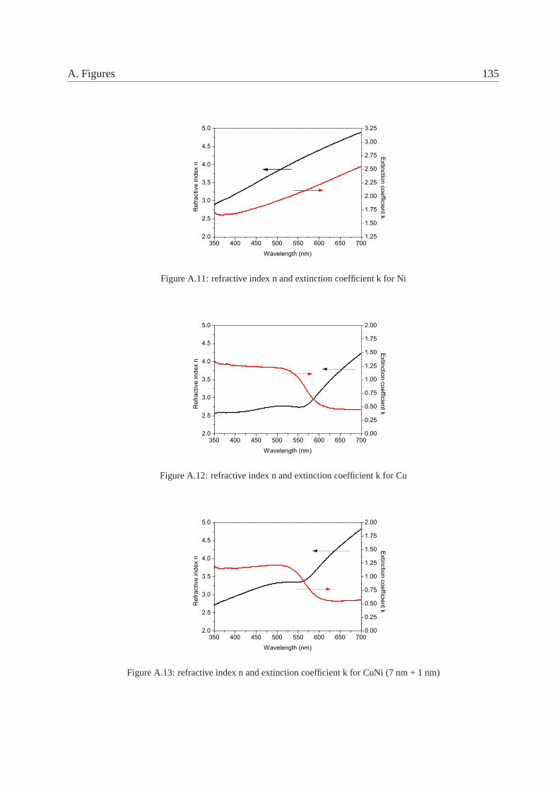
A. Figures 135
350 400 450 500 550 600 650 7002.0
2.5
3.0
3.5
4.0
4.5
5.0
Ref
ract
ive
inde
x n
Wavelength (nm)
1.25
1.50
1.75
2.00
2.25
2.50
2.75
3.00
3.25
Extinction coefficient k
Figure A.11: refractive index n and extinction coefficient kfor Ni
350 400 450 500 550 600 650 7002.0
2.5
3.0
3.5
4.0
4.5
5.0
Ref
ract
ive
inde
x n
Wavelength (nm)
0.00
0.25
0.50
0.75
1.00
1.25
1.50
1.75
2.00
Extinction coefficient k
Figure A.12: refractive index n and extinction coefficient kfor Cu
350 400 450 500 550 600 650 7002.0
2.5
3.0
3.5
4.0
4.5
5.0
Ref
ract
ive
inde
x n
Wavelength (nm)
0.00
0.25
0.50
0.75
1.00
1.25
1.50
1.75
2.00
Extinction coefficient k
Figure A.13: refractive index n and extinction coefficient kfor CuNi (7 nm + 1 nm)

A. Figures 136
350 400 450 500 550 600 650 7000.0
0.2
0.4
0.6
0.8
1.0
MEH-PPV Alq3 9% 60%
norm
. Tra
nsm
ittan
ce (a
.u.)
Wavelength (nm)
Figure A.14: Transmission spectrum for polymer blends
350 400 450 500 550 600 650 7000.0
0.2
0.4
0.6
0.8
1.0 MEH-PPV Alq3 9% 60%
norm
. Ref
lect
ance
(a.u
.)
Wavelength (nm)
Figure A.15: Reflection spectrum for polymer blends

Appendix B
Tables
f1 (%) t1 (ns) f2 (%) t2 (ns) f3 (%) t3 (ns)
9 % 4.6 0.09 73 0.14 22 0.45
60 % 40 0.25 23 1.3 37 6.3
Table B.1: PL decay for blended MEH-PPV at different concentrations: excitation wavelength 400 nm, recorded
emission wavelength 530 nm
f1 (%) t1 (ns) f2 (%) t2 (ns) f3 (%) t3 (ns)
0 % 63.6 0.15 30.9 0.42 5.5 1.1
9 % 71.8 0.14 25.9 0.4 2.3 1.5
60 % 37.0 0.16 50.1 0.47 2.9 1.98
Table B.2: PL decay for blended MEH-PPV at different concentrations: excitation wavelength 400 nm, recorded
emission wavelength 570 nm
f1 (%) t1 (ns) f2 (%) t2 (ns) f3 (%) t3 (ns)
9 % 38.2 0.03 41.3 0.20 20.5 0.53
60 % 30.5 0.04 51.6 0.31 17.9 0.74
Table B.3: PL decay for blended MEH-PPV at different concentrations: excitation wavelength 500 nm, recorded
emission wavelength 530 nm

B. Tables 138
f1 (%) t1 (ns) f2 (%) t2 (ns) f3 (%) t3 (ns)
0 % 42.1 0.07 53.0 0.38 4.9 1.2
9 % 52.4 0.11 44.6 0.38 3.0 1.3
60 % 23.8 0.09 67.9 0.39 8.3 1.13
Table B.4: PL decay for blended MEH-PPV at different concentrations: excitation wavelength 500 nm, recorded
emission wavelength 570 nm

Appendix C
Transfer Matrix Formalism
The transfer matrix formalism has been used in the simulation software Setfos 3.3 (Fluxim) for
the calculation of the passive optics properties of thin multilayer structures [155]. The reflectivity
R, the absorption A and the transmission T of a multilayer structure can been calculated by
considering the complex refractive index and the thicknessof each layer. Assuming a multilayer
system with N layers, each of those with a thickness di and complex refractive index ni .
A transfer matrix for each interface and layers can be calculated and as a result, the complete
transfer matrix can be obtained by simply multiplying each single transfer matrix [156]. The
optical stack can be described as follow:
n(x) = n0, x < x0,
n1, x0 < x < x1,
.
.
.
nN, xN−1 < xi ,
(C.1)
First, we consider an individual transfer matrix through one interface between the layer i and
the layer j. The amplitudes of the forward (indicated as F) and of the backward (indicated as B)

C. Transfer Matrix Formalism 140
propagating wave in a given direction can be expressed in thefollowing way [157][158]:
[
EF(x+i )
EB(x−i )
]
= T0N
[
EF(xN −1+)
EB(xN −1+)
]
=
[
ti j r ji
r i j t ji
][
EF(x−i )
EB(x+i )
]
(C.2)
The Fresnel coefficients for the TE-polarization would be [156][157]:
r i j =ni cosθi − n j cosθ j
ni cosθi + n j cosθ j(C.3)
ti j = 1+ r i j (C.4)
and for the TM-polarization [156][157]:
r i j =n j cosθi − ni cosθ j
n j cosθi + ni cosθ j(C.5)
ti j =ni
n j+ r i j (C.6)
the symmetry relation of the Fresnel coefficients simplifiesthe equation C2:
r i j = − r ji (C.7)
ti j t ji − r i j r ji = 1 (C.8)
so that we obtain:
[
EF(x−i )
EB(x−i )
]
=1ti j
[
1 r i j
r i j 1
][
EF(x+i )
EB(x+i )
]
(C.9)

C. Transfer Matrix Formalism 141
with the transfer matrix Ti j for the wave propagation through the interface between the layer i
and j:
Ti j =1ti j
[
1 r i j
r i j 1
]
(C.10)
the same can be applied for the propagation of the wave through the layer i, with the result
[156][157]:
Ti =
[
ej kx,i di 0
0 ej kx,i di
]
(C.11)
multiplying all transfer matrices, for each interface and for each layer, results in the Transfer-
Matrix T0N from equation C2:
T0N = T01T1T12...T(N−1)N (C.12)
The exact evaluation of the thickness, the transmittance, the reflection and the complex refractive
index of each layer used in the OLED stack is crucial for the calculation of the amplitude of the
reflected and transmitted wave through the stack. The software Setfos uses the prior measured
parameters for the calculation of the influence of the passive optics on the propagating light beam
through the media.

Bibliography
[1] C. W. Tang, S.A. VanSlyke. Appl. Phys. Lett. 51 913, (1987).
[2] J. H. Burroughes, D. D. C. Bradley, A. R. Brown, R. H. Marks, K. Mackay, R. H. Friend,
P. L. Burns and A. B. Holmes, Nature 347, p.539 (1990).
[3] C. Zhong, C. Duan, F. Huang, H. Wu, Y. Cao, Chem. Mater. 23, p.326 (2011).
[4] J. Shinar, R. Shinar, J. Phys. D: Appl. Phys. 41, p133001 (2008).
[5] M. Riede, B. Lüssem, K. Leo, Comprehensive Semiconductor Science and Technology 4,
p.448 (2011).
[6] R. H. Friend, R. W. Gymer, A. B. Holmes, J. H. Burroughes, R. N. Marks, C. Taliani, D.
D. C. Bradley, D. A. Dos Santos, J. L. Brédas, M. Lögdlund, W. R. Salaneck, Nature 397,
p.121 (1999).
[7] K. Meerholz, Nature 437, p.327 (2005).
[8] R. Das, P. Harrop, Organic & Printed Electronics Forecasts, Players & Opportunities
2007-2027, IDTechEx Ltd.
[9] T. Sasaoka, M. Sekiya, A. Yumoto, J. Yamada, T. Hirano, Y.Iwase, T. Yamada, T.
Ishibashi, T. Mori, M. Asano, S. Tamura, T. Urabe, SID Symposium Digest of Techni-
cal Papers 32, 384 (2001).
[10] A. Mikami, T. Koshiyama, T. Tsubokawa, Jpn. J. Appl. Phys. 44, p.608 (2005).
[11] M. Eritt, C. May, K. Leo, M. Toerker, C. Radehaus, Thin SolidFilms, 518 (11), p.3042
(2010).
142
Bibliography 143
[12] F. M. Tseng, A.-C. Cheng, Y.-N. Peng, Technological Forecasting and Social change 76,
p.897 (2009).
[13] J. Shinar, R. Shinar, Comprehensive Nanoscience and Technology, V.1, p.73 (2010).
[14] S.-H. Eom, E. Wrzesniewski, J. Xue, Organic Electronics12, p. 472 (2011).
[15] H.-Y. Lin, J.-H. Lee, M.-K. Wei, C.-L. Dai, C.-F. Wu, Y.-H.Ho, H.-Y. Lin, T.-C. Wu,
Optics Communications 275, p.464 (2007).
[16] R. Bathelt, D. Buchhauser, C. Gärditz, R. Paetzold, P. Weilmann, Organic Electronics 8,
p.293 (2007).
[17] K. Saxena, V. K. Jain, D. S. Mehta, Optical Materials 32,p.221 (2009).
[18] H. Hosono, Thin Solid Films 515, p.6000 (2007).
[19] J. Jancar, J. F. Douglas, F. W. Starr, S. K. Kumar, P. Cassagnau, A. J. Lesser, S. S. Stern-
stein, M. J. Buehler, Polymer 51, p.3321 (2010).
[20] F. So, B. Krummacher, M. K. Mathai, D. Poplavskyy, S. A. Choulis, V.-E. Choong, J.
Appl. Phys. 102, 091101 (2007).
[21] A. Köhler, H. Bässler, Materials Science and Engineering R 66, p.71 (2009).
[22] F. Schindler, Dissertation, Ludwig-Maximilians-Universität München (2006).
[23] M. Hoffmann, Script; Organic Semiconductors, Institut für Angewandte Photophysik, TU
Dresden (2006).
[24] S. A. Benning, Dissertation, University Paderborn (2004).
[25] N. C. Giebink, Y. Sun, S. R. Forrest, Organic Electronics 7, p.375 (2006).
[26] B. Wardle: "‘Principles and Applications of Photochemistry"’, John Wiley & Sons, Ltd.
(2009).
[27] F. Kozlowski, Dissertation, Technische Universität,TU Dresden (2005).
[28] M. Gross, Dissertation, Ludwig-Maximilians-Universität München (2006).
[29] I.-S. Park, S.-R. Park, D.-Y. Shin, J.-S. Oh, W.-J. Song,J.-H. Yoon, Organic Electronics
11, p.218 (2010).

Bibliography 144
[30] S. - A. Chen, T. - H. Jen, H. - H. Lu, J. Chin. Chem. Soc., Vol. 57, No. 3B, p. 439 (2010).
[31] F. Laquai, Dissertation, Johannes-Gutenberg-Universität, Mainz (2006).
[32] M. G. Kaplunov, S. S. Krasnikova, S. L. Nikitenko, N. L. Sermakasheva, I. K.
Yakushchenko, Nanoscale Res Lett. 7, p.206 (2012).
[33] P. S. Davids, S. M. Kogan, I. D. Parker, D. L. Smith, Appl.Phys. Lett. 69 (15), (1996).
[34] Y. Kawabe, G. E. Jabbour, S. E. Shaheen, B. Kippelen, N. Peyghambarian, Appl. Phys.
Lett. 71 (10) (1997).
[35] H. Bässler, Poly. Adv. Technol, 9, 402, (1998).
[36] A. B. Walker, A. Kambili, S. J. Martin, J.Phys.: Condens. Matter 14, p.9825 (2002).
[37] D. M. Taylor, IEEE Transactions and Electrical Insulation, Vol.13, No.5, (2006).
[38] W. D. Gill, J. Appl. Phys., Vol.43, No.12 (1972).
[39] P. M. Borsenberger, J. Appl. Phys., Vol. 68, No. 11, p.5682 (1990).
[40] R. H. Parmenter, W. Ruppel, J. Appl. Phys., Vol.30, No.10 (1959).
[41] P. W. M. Blom, M. J. M. de Jong, J. J. M. Vleggaar, Appl. Phys. Lett. 68, (23), p.3308
(1996).
[42] W. L. Barnes, J. Lightwave Technol. 17 (11), p.2170 (1999).
[43] S. Möller, S. R. Forrest, J. Appl. Phys., Vol. 91, No. 5, (2002).
[44] H. Greiner, Jpn. J. Appl. Phys. 46 (No. 7A), 4125 (2007).
[45] John C. Ho, PhD-Thesis, MIT (2004).
[46] S. Asada, IEEE Journal of Quantum Electronics 27 (4), 884 (1991).
[47] C. Genet, T. W. Ebbesen, Nature 445 (7123), 39 (2007).
[48] P. A. Hobson, S. Wedge, J. A. E. Wasey, I. Sage, W. L. Barnes, Adv. Mater. 14 (19), p.1393
(2002).
[49] F. Flory, L. Escoubas, Gerard Berginc, Journal of Nanophotonics, Vol. 5, 052502-1 (2011).

Bibliography 145
[50] M.-K. Wei, C.-W. Lin, C.-C. Yang, Y.-W. Kiang, J.-H. Lee, H.-Y. Lin, Int. J. Mol. Sci. 11,
p.1527 (2010).
[51] N. Takada, T. Tsutsui, S. Saito, Appl. Phys. Lett. 63, p.2032 (1993).
[52] J. C. Manifacier, J. Gasiot, J. P. Fillard, Journal of Physics E, 9, p.1002 (1976).
[53] C. A. Wilson, R. K. Grubbs, S. M. George, Chem. Mater. 17, p.5625 (2005).
[54] Jill Svenja Becker, PhD Thesis, Harvard University (2002).
[55] Viljami Pore, PhD Thesis, University of Helsinki (2010).
[56] S. M. George, Chem. Rev., Vol. 110, No. 1, p.111 (2010).
[57] M. D. Groner, F. H. Fabreguette, J. W. Elam, S. M. George,Chem. Mater., Vol. 16, No. 4,
p.639 (2004).
[58] R. L. Puurunen, W. Vandervorst, J. Appl. Phys. 96, p.7686(2004).
[59] J. D. Ferguson, A. W. Weimer, S. M. George, Chem. Mater. 16, p.5602 (2004).
[60] K. Neyts, A. U. Nieto, J. Opt. Soc. Am. A, Vol.23, No.5 (2006).
[61] K. Saxena, V. K. Jain, D. S. Mehta, Optical Materials 32,p.221, (2009).
[62] S. M. Jeong, F. Araoka, Y. Machida, K. Ishikawa, H. Takezoe, S. Nishimura, G. Suzaki,
Appl. Phys. Lett. 92, p.083307 (2007).
[63] C. F. Madigan, M.-H. Lu, J. C. Sturm, Appl. Phys. Lett. 13, p.1650 (2000).
[64] Y. Sun, S. R. Forrest , Journal of Applied Physics 100, p.073106 (2006).
[65] Y. Sun, S. R. Forrest, Nature Photonics 2, p.483 (2008).
[66] J. Meyer, P. Görrn, S. Hamwi, H.-H. Johannes, T. Riedl, W.Kowalsky, Appl. Phys. Lett.
93, p.073308 (2008).
[67] J. J. Berry, D. S. Ginley, P. E. Burrows, Appl.Phys.Lett. 92, p.193304 (2008).
[68] Y. Tomita, C. May, M. Toerker, J. Amelung, M. Eritt, F. Loeffler, C. Luber, K. Leo, K.
Walzer, K. Fehse, Q. Huang, Appl. Phys. Lett. 91, p.063510 (2007).

Bibliography 146
[69] C. D. Williams, R. O. Robles, M. Zhang, S. Li, R. H. Baughman, A.A. Zakhidov, Appl.
Phys. Lett. 93 183506 (2008).
[70] Y. Wang, C. A. Di, Y. Liu, H. Kajiura, S. Ye, L. Cao, D. Wei, H.Zhang, Y. Li, K. Noda,
Adv. Mater. 20 4442-9 (2008).
[71] Z. Wu, Z. Chen, X. Du, J. M. Logan, J. Sippel, M. Nikolou, K.Kamaras, J. R. Reynolds,
D. B. Tanner, A. F. Hebard, A. G. Rinzler, Science 305, No. 5688,p.1273 (2004).
[72] J. Meiss, M. K. Riede, K. Leo, Appl. Phys. Lett. 94, p.013303 (2009).
[73] B. O’Connor, C. Haughn, K. - H. An, K. P. Pipe, M. Shtein, Appl. Phys. Lett.93, p.223304
(2008).
[74] H. Peng, X. Zhu, J. Sun, Z. Xie, S. Xie, M. Wong, H.-S. Kwok, Appl. Phys. Lett. 87,
p.173505 (2005).
[75] S. Giurgola, A. Rodríguez, L. Martínez, P. Vergani, F. Lucchi, S. Benchabane, V. Pruneri,
J. Mater. Sci: Mater. Electron. 20, p.181 (2009).
[76] D. Krautz, S. Cheylan, D. S. Ghosh, V. Pruneri, Nanotechnology 20, p.275204 (2009).
[77] S. Cheylan, D. S. Ghosh, D. Krautz, T. L. Chen, V. Pruneri, Org. Electron. 12, p.818
(2011).
[78] L. Martinez, D. S. Ghosh, S. Giurgiola, P. Vergani, V. Pruneri, Opt. Mater. 31, p.1115
(2009).
[79] A. B. Walker, A. Kambili, S. J. Martin, J.Phys.: Condens. Matter 14, p.9825 (2002).
[80] S. Nowy, N. A. Reinke, J. Frischeisen, W. Brütting, Proc. of SPIE Vol. 6999, 69992V,
(2008).
[81] G. K. Hall, C. H. B. Mee, Phys.Status.Solidi.a 5, p.389 (1971).
[82] H. Hornauer, J. Vancea, G. Reiss, H. Hoffmann, Zeitschrift für Physik, B: Condensed
Matter 77(3), p.399 (1989).
[83] G. Haacke, J. Appl. Phys. 47, 4086 (1976)
[84] U. Scherf, E. J. W. List, Adv. Materials 14, No. 7, p.477 (2002).
[85] N. A. Reinke, C. Ackermann, W. Brütting, Optics Communications 266, p.191 (2006).

Bibliography 147
[86] P. E. Burrows, Z. Shen, V. Bulovic, D. M. McCarty, S. R. Forrest, J. A. Cronin, M. E.
Thompson, J. Appl. Phys., Vol. 79, No. 10, p.7991 (1996).
[87] Y. - R. Jeng, M. - L. Guo, H. - C. Li, T. - F. Guo, Electrochemical and Solid-State Letters,
10 (12), p.139 (2007).
[88] K. Hong, J. - L. Lee, Electron. Mater. Lett. Vol. 7, No. 2,p.77 (2011).
[89] S. H. Kim, J. Jang, J. Y. Lee, Appl. Phys. Lett. 91, p.103501 (2007).
[90] M. Kuik, L. J. A. Koster, A. G. Dijkstra, G. A. H. Wetzelaer, P. W. M. Blom, Organic
Electronics 13, p.969 (2012).
[91] B. Perucco, N. A. Reinke, D. Rezzonico, M. Moos, B. Ruhstaller, Optics Express 18,
(2010).
[92] G. G. Malliaras, J. C. Scott, J. Appl. Phys., Vol. 85, No. 10, p.7426, (1999).
[93] S. Woo, J. Kim, G. Cho, K. Kim, H. Lyu, Y. Kim, Journal of Industrial and Engineering
Chemistry 15, p.716 (2009).
[94] Y. Iwama, D. C. Cho, T. Mori, T. Mizutani, Proceedings of the 7th Intemational Confer-
ence on Properties and Applications of Dielectric Materials, Nagoya (2003).
[95] A. Benor, S.-Y. Takizawa, C. Perez-Bolivar, P. Anzenbacher Jr., Organic Electronics 11,
p.938 (2010).
[96] S. Y. Kim, J. - L. Lee, K. - B. Kim, Y. - H. Tak, J. Appl. Phys.,Vol. 95, No. 5, (2004).
[97] M. G. Helander, Z. - B. Wang, M. T. Greiner, Z. - W. Liu, J. Qiu, Z. - H. Lu, Adv. Mater.
22, p.2037 (2010).
[98] K. Tamano, D.-C. Cho, T. Mori, T. Mizutani, M. Sugiyama, Thin Solid Fims 438, 182
(2003).
[99] C.-W. Chen, P.-Y. Hsieh, H.-H. Chiang, C.-L. Lin, H.-M. Wu, C.-C. Wu, Appl. Phys. Lett.
83, 5127 (2003).
[100] G. Papadimitropoulos, N. Vourdas, V. E. Vamvakas, D. Davazoglou, J. Phys.: Conf. Ser.
10 p.182 (2005).

Bibliography 148
[101] D. S. Gosh, R. Betancur, T. L. Chen, V. Pruneri, J. Martorell, Sol. Energy Mater. Sol. Cells
95, p.1228 (2011).
[102] D.S. Ghosh, T.L. Chen, V. Pruneri, Appl. Phys. Lett. 96,091106 (2010).
[103] Z. B. Wang, M. G. Helander, J. Qiu, D. P. Puzzo, M. T. Greiner, Z. M. Hudson, S. Wang,
Z. W. Liu, Z. H. Lu, Nature Photonics 5, p.753 (2011).
[104] S. K. So, W. K. Choi, C. H. Cheng, L. M. Leung, C. F. Kwong, Appl. Phys. A 68, p.447
(1999).
[105] J.S. Kim, R.H. Friend, F. Cacialli, Synthetic Metals 111-112, p.369 (2000).
[106] R. H. Jordan, A. Dodabalapur, R. E. Slusher, Appl. Phys. Lett. 69, p.1997 (1996).
[107] E. F. Shubert, N. E. J. Hunt, M. Micovic, R. J. Malik, D. L.Sivco, A. Y. Cho, G. J. Zydzik,
Science 265 p.943 (1994).
[108] Y. Sun, N. C. Giebink, H. Kanno, B. Ma, M. E. Thompson, S. R. Forrest, Nature 440, 908
(2006).
[109] S. Reineke , F. Lindner , G. Schwartz , N. Seidler , K. Walzer , B. Lüssem , K. Leo , Nature
459, 234 (2009).
[110] S. Y. Ryu, J. T. Kim, J. H. Noh, B. H. Hwang, C. S. Kim, S. J. Jo,H. Seok Hwang, S. J.
Kang, H. K. Baik, C. H. Lee, S. Y. Song, S. J. Lee, Appl. Phys. Lett. 92, 103301 (2008).
[111] M. Zhang, S. Xue, W. Dong, Q. Wang, T. Fei, C. Gu, Y. Ma, Chem. Commun. 46, 3923
(2010).
[112] N. Rehmann, C. Ulbricht, A. Köhnen, P. Zacharias, M. C. Gather, D. Hertel, E. Holder, K.
Meerholz, U. S. Schubert, Adv. Mat. 20, p.129 (2008).
[113] L. Duan, L. Hou, T. - W. Lee, J. Qiao, D. Zhang, G. Dong, L.Wanga, Y. Qiu, J. Mater.
Chem., 20, p.6392 (2010).
[114] S.-R. Tseng, H.-F. Meng, K.-C. Lee, S.-F. Horng, Appl. Phys. Lett. 93, 153308 (2008).
[115] US Patent 7063994 - Organic semiconductor devices andmethods of fabrication including
forming two parts with polymerisable groups and bonding theparts.

Bibliography 149
[116] C.-Y. Chang, F.-Y. Tsai, S.-J. Jhuo, M.-J. Chen, Organic Electronics 9, Issue 5, p.667
(2008).
[117] J. C. Bernède, A. Godoy, L. Cattin, F. R. Diaz, M. Morsli and M. A. del Valle (2010).
Organic Solar Cells Performances Improvement Induced by Interface Buffer Layers, Solar
Energy, Radu D Rugescu (Ed.), ISBN: 978-953-307-052-0, InTech.
[118] J. W. Elam, S. M. George, Chem. Mater., Vol. 15, No. 4, p.1020 (2003).
[119] S. D. Elliott, G. Scarel, C. Wiemer, M. Fanciulli, G. Pavia, Chem. Mater., Vol. 18, No. 16,
p.3764 (2006).
[120] B. D. Chin, N. S. Kang, J.-W. Yu, S. M. Jo, J. Y. Lee, J. Appl.Phys. 102, p.024506 (2007).
[121] M.D. Groner, F.H. Fabreguette, J.W. Elam, S.M. George, Chem. Mater. 16, p.639 (2004).
[122] T. - W. Lee, O. O. Park, Adv. Mater. 12, No. 11, p.801 (2000).
[123] Z. B. Deng, X. M. Ding, S. T. Lee, W. A. Gambling, Appl. Phys. Lett. 74, p.2227 (1999).
[124] H. C. Lin, P. D. Yea, G. D. Wilk, Appl. Phys. Lett. 87, p.182904 (2005).
[125] C. Zhong, C. Duan, F. Huang, H. Wu, Y. Cao, Chem. Mater., Vol.23, No. 3, p.326 (2011).
[126] J. - D. You, S. - R. Tseng, H. - F. Meng, F. - W. Yen, I. - F. Lin, S. - F. Horng, Organic
Electronics 10, p.1610 (2009).
[127] S. - M. Cho, J. - H.Bae, E. Jang, M. - H. Kim, C. Lee, S. - D. Lee,Semicond. Sci. Technol.
27, p.125018 (2012).
[128] C. Zhang, S. Liu, F. Wang, Y. Zhang, Microelectronics Journa l39, p.1525 (2008).
[129] T. - C. Lin, C. - H. Hsiao, J. - H. Lee, Proc. of SPIE Vol. 5937, 59371Q, (2005).
[130] PhD-Thesis, Stefan Nowy, University Augsburg (2010).
[131] J. C. Scott, P. J. Brock, J. R. Salem, S. Ramos, G. G. Malliaras, S. A. Carter, L. Bozano,
Synthetic Metals 111-112, p.289 (2000).
[132] J. H. Ahn, C. Wang, C. Pearson, M. R. Bryce, M. C. Pettya, Appl.Phys. Lett., Vol. 85,
No. 7, p.1283 (2004).

Bibliography 150
[133] L. D. Bozano, K. R. Carter, V. Y. Lee, R. D. Miller, R. DiPietro, J. C. Scott, J. Appl. Phys.,
Vol. 94, No. 5, p.3061 (2003).
[134] S. de F. C. da Silva, M. Foschini, H. S. Silva, J. R. Tozoni,F. A. Castro, R. A. Silva, A.
Marletta, Organic Electronics 13, p.2935 (2012).
[135] D. Y. Kim, J. K. Grey, P. F. Barbara, Synthetic Metals 156, p.336 (2006).
[136] P. Cea, Y. Hua, C. Pearson, C. Wang, M. R. Bryce, F. M. Royo, M. C. Petty, Thin Solid
Films 408. p.275 (2002).
[137] J. H. Ahn, C. Wang, N. E. Widdowson, C. Pearson, M. R. Bryce, M. C. Petty, Journal of
Applied Physics 98, p.054508 (2005).
[138] G. Saygili, C. Varlikli, C. Zafera, C. Ozsoya, Synthetic Metals 162, p.621 (2012).
[139] D. Krautz, E. Lunedei, J. Puigdollers, G. Badenes, R. Alcubilla, S. Cheylan, Appl. Phys.
Lett. 96, p.033301 (2010).
[140] R. Jakubiak, C. J. Collison, W. C. Wan, L. J. Rothberg, and B. R. Hsieh, J. Phys. Chem. A
103, 2394 (1999).
[141] V. Sholin, E. J. Lopez-Cabarcos, S. A. Carter, Macromolecules, Vol. 39, No. 17, p.5830
(2006).
[142] Y. Shi, J. Liu, Y. Yang, J. Appl. Phys., Vol. 87, No. 9, p.4254 (2000).
[143] K. Thangaraju, J. Kumar, P. Amaladass, A. K. Mohanakrishnan, V. Narayanan, Appl.
Phys. Lett. 89, p.082106 (2006).
[144] C. A. Amorim, M. R. Cavallari, G. Santos, F. J. Fonseca, A. M. Andrade, S. Mergulhão,
Journal of Non-Crystalline Solids 358, p.484 (2012).
[145] A. Fuchs, T. Steinbrecher, M. S. Mommer, Y. Nagata, M. Elstner, C. Lennartz, Phys.
Chem. Chem. Phys. 14, p.4259 (2012).
[146] K. - H. Choi, D. - H. Hwang, H. - M. Lee, L. - M. Do, T. Zyung, Synthetic Metals 96,
p.123 (1998).
[147] R. Jakubiak, C. J. Collison, W. C. Wan, L. J. Rothberg, and B. R. Hsieh, J. Phys. Chem. A
103, 2394 (1999).

Bibliography 151
[148] K. - M. Yeh, Y. Chen, Organic Electronics 9, p.45 (2008).
[149] M. Valadares, I. Silvestre, H. D. R. Calado, B. R. A. Neves, P. S. S. Guimarães, L. A.
Cury, Materials Science and Engineering C 29, p.571 (2009).
[150] M. D. McGehee, T. Bergstedt, C. Zhang, A. P. Saab, M. B. O’Regan, G. C. Bazan, V. I.
Srdanov, A. J. Heeger, Adv. Mater. 11, No. 16, p.1349 (1999).
[151] Y. Qiu, L. Duan, X. Hu, D. Zhang, M. Zheng, F. Bai, Synthetic Metals 123, p.39 (2001).
[152] T. Q. Nguyen, I. B. Martini, J. Liu, B. J. Schwartz, J. Phys. Chem. B 104, p.237 (2000).
[153] R. Pizzoferrato, T. Ziller, A. Micozzi, A. Ricci, C. L. Sterzo, A. Ustione, C. Oliva, A.
Cricenti, Chemical Physics Letters 414, p.234 (2005).
[154] B. Ruhstaller, J. C. Scott, P. J. Brock, U. Scherf, S. A. Carter, Chem. Phys. Lett. 317, p.238
(2000).
[155] Fluxim Setfos 3.3, Handbook and Tutorial (2013).
[156] Z. Ye, PhD-Thesis, Iowa State University (2011).
[157] C. C. Katsidis, D. I. Siapkas, Applied Optics Vol. 41, No.19, p.3978 (2002).
[158] M. C. Troparevsky, A. S. Sabau, A. R. Lupini, Z. Zhang, OptExpress. 18 p.24715 (2010).

Appendix D
Publications
Talks
D. S. Ghosh, T. L. Chen, D. Krautz, S. Cheylan, V. Pruneri: "‘Environmentally stable Al –
doped ZnO transparent electrode for organic optoelectronic devices"’, Renewable Energy
and the Environment, Austin, TX, USA, 2. – 4. November 2011
D. S. Ghosh, T. L. Chen, D. Krautz, S. Cheylan, V. Pruneri: "‘Ultrathin metal for indium
free organic lighting and photovoltaics"’, Photonics 2010, 10th International conference
on fiber optics and photonics, Guwahati, India, December 2010
D. S. Ghosh, D. Krautz, S. Cheylan, V. Pruneri: "‘Ultrathin metal transparent electrodes
for lighting and photovoltaic applications"’, Optics and Photonics for Advanced Energy
Technology, Cambridge (USA), 24. June 2009
S. Cheylan, D. Krautz, J. Puigdollers, C. Voz, R. Alcubilla,G. Badenes: "‘Enhanced perfor-
mance of OLEDs using polymer blends as the active layer"’, 7th Conference on Electron
Devices (CDE 09), Santiago de Compostela, 11. – 13. February 2009
S. Cheylan, D. Krautz, J. Puigdollers, C. Voz, R. Alcubilla,G. Badenes: "‘Enhanced per-
formance of OLED based on a molecularly doped polymer"’, 1st International Symposium
on Flexible Organic Electronics (IS – FOE), Greece, Halkidiki, 9. – 11. July 2008
D. Krautz, S. Cheylan, J. Puigdollers, C. Voz, R. Alcubilla,G. Badenes: "‘Enhanced per-
formance of OLEDs based on a molecularly DOPED polymer"’, International Symposium
152

D. Publications 153
on Flexible Electronics (ISFE), Spain, Tarragona, 6. – 9. April 2008
D. Krautz, S. Cheylan, J. Puigdollers, C. Voz, R. Alcubilla,G. Badenes: "‘Polymeric Blends
for organic light emitting diodes"’, ENMM07, VIII Escuela Nacional de Materiales Molec-
ulares, Spain, Estepona, 20. – 27. May 2007
S. Cheylan, H. Bolink, A. Fraleoni – Morgera, D. Krautz, J. Puigdollers, C. Voz, L. Setti, R.
Alcubilla, G. Badenes: "‘Single layer organic light emitting diode based on a thiophene
polymer"’, CDE07, Conferencia de Dispositivos Electronicos, San Lorenzo del Escorial,
January 2007
Posters
D. Krautz, D. S. Ghosh, V. Pruneri, S. Cheylan: "‘Nickel as an alternative semitransparent
anode to Indium Tin Oxide for OLED application"’, European Conference on Molecular
Electronics – ECME09, Copenhagen, Denmark, 09. – 12. September 2009
D. Krautz, S. Cheylan, J. Puigdollers, C. Voz, R. Alcubilla,G. Badenes: "‘Enhanced perfor-
mance of OLED based on a molecularly doped polymer after thermal annealing"’, ICEL
– 7, 7th International Conference on Electroluminescence ofMolecular Materials and Re-
lated Phenomena, Dresden, Germany, 02. – 06. September 2008
D. Krautz, S. Cheylan, H. Bolink, A. Fraleoni – Morgera, J. Puigdollers, C. Voz, L. Setti,
R. Alcubilla, G. Badenes: "‘Thiophene polymer containing a cyano group as a side chain
substituent for OLED application"’, ICEO08, 4th International Conference on Organic
Electronics, Eindhoven, The Netherlands, 16. – 18. June 2008
A. Fraleoni – Morgera, S. Cheylan, D. Krautz, J. Puigdollers,L. Setti, I. Mencarelli, R.
Alcubilla, G. Badenes: "‘Photophysical properties of polythiophenes containingdiffer-
ent amounts of cyano functional group as a side chain substituent"’, EMRS08, European
Material Research Society Spring Meeting, Strasbourg, France, 26. – 30. May 2008
D. Krautz, S. Cheylan, J. Puigdollers, C. Voz, R. Alcubilla,G. Badenes: "‘Solvent influ-
ence on the performance of OLEDs based on polyfluorenes"’, WIP08, School on Photonic
Metamaterials, Paris, France, 14. – 18. April 2008

D. Publications 154
S. Cheylan, D. Krautz, J. Puigdollers, C. Voz, R. Alcubilla,G. Badenes: "‘Organic Blend
for Light Emitting Diodes"’, ECME07, European Conference on Molecular Electronics,
Metz, France, 5. – 08 September 2007
D. Krautz, S. Cheylan, H. Bolink, A. Fraleoni – Morgera, J. Puigdollers, C. Voz, L. Setti,
R. Alcubilla, G. Badenes: "‘Single layer organic light emitting diode based on a thio-
phene polymer with a cyano group"’, PHOREMOST Workshop and General Meeting,
"‘Advances in Nanophotonics"’, Vilnius, Lithuania, 26. – 28.September 2006
Papers
T. L. Chen, D. S. Ghosh, D. Krautz, S. Cheylan, V. Pruneri: "‘Highly stable Al – doped ZnO
transparent conductors using an oxidized ultrathin metal capping layer at its percolation
thickness"’, Appl. Phys. Lett. 99, (2011) 093302
S. Cheylan, D. S. Ghosh, D. Krautz, T. L. Chen, V. Pruneri: "‘Organic light – emitting diode
with indium – free metallic bilayer as transparent anode"’, Organic Electronics 12, (2011)
818
D. Krautz, E. Lunedei, J. Puigdollers, G. Badenes, R. Alcubilla, S. Cheylan: "‘Interchain
and intrachain emission branching in polymer light – emitting diode doped by organic
molecules"’, Applied Physics Letter, 96 (2010) 033301
D. Krautz, S. Cheylan, D. S. Gosh, V. Pruneri: "‘Nickel as an alternative semitransparent
anode to Indium Tin Oxide for polymer LED application"’, Nanotechnology, 20 (2009)
275204
Research Stays
15.02.2009 - 14.08.2009, Merck Chemicals Ltd, Chilworth Technical Centre, University Park-
way Southampton, SO16 7QD, United Kingdom
09.09.2008 - 10.09.2008, Chair of Display Technology, University Stuttgart, Allmandring 3b,
70569 Stuttgart, Germany
08.09.2008 - 08.09.2008, Siemens AG, Corporate Technology, Innovative Electronics, CT MM
1 Günther – Scharowsky – Str. 1, 91058 Erlangen, Germany

D. Publications 155
05.03.2007 - 09.03.2007, Chair of Display Technology, University Stuttgart, Allmandring 3b,
70569 Stuttgart, Germany