Embed Size (px)
Citation preview

HP Archive
This vintage Hewlett Packard document waspreserved and distributed by
www.hparchive.com
Please visit us on the web !
Scanned by on-line curator: Tony Gerbic
** For FREE Distribution Only ***

HEWLETT-PACKARD COMPANY
4.2A/4.4ATRAVELING-VVAVEAMPLIFIER
)
)
)
00144·2
OPERATING AND SERVICE MANUAL
MODEL 492A
AND
MODEL 494A
SERIALS PREFIXED: 010-
TRAVELING-WAVE AMPLIFIERS
Copy,;gh' HEWLETT.'ACICA.D COM' ANY 1962lS01 'AGE MILL ROAD, 'ALO ALTO, CALlFO.NIA, U.S.A.
Printed: JAN 1962

Model 492Aj494A Table of ContentsLists of Illustrations and Tables
TABLE OF CONTENTS
Section Page Section PageI GENERAL INFORMATION 1-1 IV PRINCIPLES OF OPERATIO (cont'd)
1-1. Description 1-1 4-10. Traveling Wave Tube 4-11-6. Instrument Identification 1-2 4-15. Grid Modulation. 4-41-8. Traveling Wave Tube Warranty 1-2 4-17. Helix Modulation · . 4-4
4-22. Constant-Amplitude, LinearII INSTALLATION 2-1 Sawtooth Generator 4-5
2-1. Mechanical Inspection 2-12-3. Power Requirements. 2-1 V MAINTENANCE. 5-12-5. Power Cable. 2-1 5-1. Introduction. · 5-12-8. Installation 2-1 5-3. Cleaning the Air Filter· 5-12-12. Repackaging for Shipment 2-1 5-5. Test Equipment . 5-1
5-7. Repair. 5-3III OPERATING INSTRUCTIONS 3-1 5-8. Cabinet Removal 5-3
3-1. Introduction . 3-1 5-10. Tube Replacement . . 5-33-3. Preliminary Operating Procedure 3-1 5-12. Traveling Wave Tube Capsule3-6. Helix Control 3-1 Replacement 5-33-8. Saturation Power Output 3-1 5-17. Changing the Frequency Range3-12. Bandwidth Considerations . 3-1 of the 492A or 494A 5-53-14. Constant Gain or Constant Output 5-21. Adjustments 5-5
Amplification 3-3 5-22. Excessive Helix Current 5-53-18. Buffer Amplifications 3-3 5-24. Chassis Helix Control 5-53-20. Amplitude Modulation 3-3 5-26. Anode Voltage Control . 5-53-24. Pulse Modulation. 3-6 5-28. Regulated Power Supply 5-53-27. Limited Phase Modulation. 3-6 5-30. Troubleshooting. · 5-63-29. Unlimited Phase Modulation and 5-32. Performance Checks 5-7
Frequency Shifting . 3-6 5-33. Gain Check. 5-73-34. Homodyne Detection 3-7 5-36. Output Power Check 5-73-37. Frequency Modulation 3-9 5-39. Noise Figure Check 5-7
5-42. Hum and Spurious Modulation Check· 5-8
) IV PRINCIPLES OF OPERATION. 4-14-1. Introduction . 4-1 VI REPLACEABLE PARTS . 6-14-3. Magnet Power Supply. 4-1 6-1. Introduction 6-14-5. Regulated Power Supply 4-1 6-4. Ordering Information 6-1
LIST OF ILLUSTRATIONS AND TABLES
Number Illustration Title Page4-3. Cutaway View ofaTWT Capsule and Magnet
Showing the Important Elements· . . . 4-34-4. Cutaway View of an Encapsulated TWT· . 4-34-5. Simplified Circuit of a Constant Amplitude,
Variable Slope Sawtooth Generator·· 4-55-1. Top View of Models 492A and 494A ., 5-25-2. Bottom View Looking Towards the Front
Panel of Models 492A and 494A . .. 5-45-3. Rear View of Models 492A and 494A" 5-45-4. Test Setup for Gain, Output Power, and
Noise Figure Performance Checks 5-75-5. Test Setup for Hum and Spurious
Modulation Performance Check . . 5-85-6. Models 492A and 494A Schematic Diagram' 5-9
Number Illustration Title Page1-1. Model 492A Traveling Wave Amplifier 1-11-2. Traveling Wave Tube Warranty 1-23-1. Operating Controls . 3-03-2. Typical Gain and Power Output
Characteristics . 3-23-3. Block Diagram of a Circuit used to
Maintain Constant-Level Output Powerfrom a TWT Amplifier 3-3
3-4. Block Diagram of an Automatic GainControl to Maintain Constant Ampli-fication from a TWT Amplifier 3-3
3-5. Typical Plot of Output Voltage vs GridVoltage of a Model 492A 3-4
3-6. Typical Plot of Output Voltage vs GridVoltage of a Model 494A. 3-5
3-7. RF Phase Shift Produced by Helix Mod 3-73-8. Offset Frequency Produced by Sawtooth
Modulation of the Helix . 3-73-9. Block Diagram of a Linear (Homodyne)
) Detection System. 3-83-10. Block Diagram of a Circuit to Produce
an FM Signal with a TWT Amplifier 3-84-1. Block Diagram, Models 492A and 494A 4-04-2. TWT and How it Works . 4-2
00144-2
1-1.3-1.
5-1.5-2.5-3.6-1.6-2.
Table TitleSpecifications. . . . . .Maximum Operating Currents for
Models 492A and 494A . . .Recommended Test EquipmentTube Replacement ListTroubleshooting Chart . . •Reference Designation IndexReplaceable Parts· . . . .
1-0
3-15-15-35-66-26-5
iii

Section ITable 1-1
Model 492A/494A
Table 1-1, Specifications
~ Model 492A <Fj! Model 494A
Frequency Range: 4 gc to 8 gc 7 gc to 12,4 gc
Maximum Output Power: 20 mw minimum into 50 ohm load 20 mw minimum into 50 ohm load
Modulated Pulse Delay: Approximately 20 ns Approximately 15 ns
Helix Modulating Voltage: Approximately 40 volts peak-topeak. Provides 3600 phase shift.Input impedance lOOK
Approximately 50 volts peak-topeak. Provides 3600 phase shift.Input impedance lOOK
Hum and Spurious Modulation: At least 45 db below signal level At least 45 db below signal level
Weight:
Power Supply:
66 lb net, 85 Ib shipping
US volts ±10%, 50 to 60 cps,approximately 200 watts
63 Ib net, 84 Ib shipping
U5 volts ±10%, 50 to 60 cps,approximately 225 watts
Accessories Furnished: AC-16Q cable assembly AC-l6Q cable assembly
For Both Models
Small Signal Gain: 30 db minimum
Meter Monitors: Cathode current, anode current, helix current, collector current.
Input Impedance: 50 ohms, swr less than 2
Output Internal Impedance: 50 ohms, swr less than 3
Dimensions: Cabinet Mount: 7-3/8 in.wide, U-l/2 in.high, 20 in.deep.
TypeN
Less than 30 db
t
:0: IU]REAR ,~,,".:0: '.1&
1.----19---.,492AR/494AR
Rack Mount:
Noise Figure:
Connectors,RF Input and Output:
Pulse Rise and Decay Time:
Amplitude Modulating Voltage:
Approximately 15 ns
Approximately 50 volts peak positive pulse will produce a 40 db changein rf power output. Sensitivity approximately 1 db/volt
1-0 00144-2

Model 492A/494A
SECTION I
GENERAL INFORMATION
Section IParagraphs 1-1 to 1-4
1-1. DESCRIPTION.
1-2. The t$ Models 492A and 494A Traveling WaveAmplifiers are broadband, linear amplifiers providing adjustable amplification up to at least 30 db, between 4 and 12.4 gc, and have a maximum power output of at least 20 milliwatts to an external load of 50ohms. The frequency range of the t$ Model 492A is4 to 8 gc; the frequency range of the Model 494A is 7to 12.4 gc. These traveling wave tube (twt) amplifiers are designed to be used also as buffer amplifiersor modulators for any signal within their frequencyrange. As buffers, their input impedances remainconstant with any reasonable load change at the outputterminal; the attenuation between input and output signals is at least 60 db, minus the gain of the amplifier.As modulators, they can be used to amplitude, frequency, pulse, or phase modulate the signal beingamplified with no interaction on the signal source.The gain and power output of the amplifiers are continuously adjustable by the front panel GRID BIAS control. Hum and spurious modulation generated withinthe amplifiers are at least 45 db below the output signal level and the noise figure is less than 30 db.
1-3. The t$ Models 492A and 494A Traveling WaveAmplifiers, amplify any type of rf signal: cw, swept,sine-modulated, pulsed, multiple signals on differentfrequencies, etc. A twt amplifier used as a modulator,in conjunction with a signal generator, can be used toamplitude modulate an rf carrier to approximately 30%with less than 2.5% harmonic distortion and up to 50%with less than 5% distortion. Amplitude modulationsensitivity is approximately 1 db/volt. Pulse modulation is excellent; the rise time is less than 15 ns.Phase modulation up to 3600 with less than 1 dbamplitude modulation is also possible. Wide-bandfrequency modulation is simulated by a step-wise phasemodulation described in section Ill.
1-4. The front panel meter is provided for checkingand adjusting electrode currents in the traveling-wavetube. The meter helps to obtain desired operatingcharacteristics during normal operation of the amplifier and also assists with preventive maintenance andtroubleshooting. An anode voltage adjustment on theinstrument chassis prOVided to adjust the cathodecurrent of the twt back to normal due to tube ageing.
)
00144-2
Figure 1-1. Model 492A Traveling Wave Amplifier
1-1

Section IParagraphs 1-5 to 1-9
1-5. The ~ Model 492A and 494A are similar in thatone model may be changed to the other, by replacingthe twt, as covered in paragraph 5-17.
1-6. INSTRUMENT IDENTIFICATION.
1-7. Hewlett-Packard uses a two-section eight-digitserial number (000-00000). If the first three digitsof the serial number on your instrument do not agree
WA••ANTY CLAIM AND ADJUITMINT 'IOCIDUU
Model 492A/494A
with those on the title page of this manual, changesheets supplied with the manual will define differencesbetween your instrument and the Model 492A or 494Adescribed in this manual.
1-8. TRAVELING WAVE TUBE WARRANTY.
1-9. The Traveling Wave Tube Warranty is illustrated in figure 1-2. A sheet for your use is includedin the appendix of this manual.
MICROWAVE TUBE WARRANTY CLAIMINFORMATION FORM
IMPORTANT: Please ans....er all questions fully -- InsuHlclent Information may delay processingof your claim. -
for microwave tubes supplied by [heHEWLETT· PACKARD COMPANY
for use In *Instruments
Microwave tubes supplied by the Hewlett-Packard Company. either 88 original or replacement.for use in 8 instruments are actually warranted by the tube manufaclUrer and not by 9.However, S will process warranty claims for you, and will promptly pass on all allowancesgranted by the tube manufacturer.
In the event that your tube Is (ound to be repairable, the tube manufacturer reserves the rightto repair and return the tube in lieu of Issuing pro--Tata credil.
For your convenience, warrantyclalms(orall microwave tubes supplied by the Hewlett-PackardCompany may be made on this sIngle form; merely fJII out the lnfonnallon on the reverse sideand rerurn this fonn. along .... lth thedefectlve rube. to your 8 engineering representallve. or tO~.Please be sure each space on the form is filled In··lack of complete infonnation may delayprocessing of yourcTiim.
Each tube manufacturer has his own warranty policy. Copies of Individual Conditions of Warranty are available from your * engineering representative or from Ihe He....len·PackardCompany.
SHIPPING INSTIUCTIONS
FROM: (rube Owner)
Company
Address
Tube type
Tube serial No. _
Tube mfr.
Use in ~ Model _
Instrument serial no. _
Date
FOR FURTHER INFORMATION CONTACT:
Name _
Title _
Company _
Address _
Tube purchased from
On P. O. number
The following instructions are included to aid you In preventing damage in transit. Packageyour tube carefully •• no allowance can be made on broken tubes. Tube is Original ( ) or Replacement (
1. Carefully wrap tube in 1/4 inch thick "klmpack". Cotton batting. or other sofl paddingmaterial.
2. Wrap the above in heavy kraft paper.
3. Pack in a rigid container ....hlch Is at least 4 inches larger than the lube In each dimension.
4. Surround the tube with at least 2 inches of shock absorbing material. Be cenaln that thepacking Is tight all around the tube.
Date tube received _
Date first tested
Date placed in service _
Date of failure _
Hours use per day (average) _
Number of days In service _
Total hours filament operation
5. Tubes returned from outside the continental UnltedSrates should be packed In a wooden box.
6. Mark container FRAGILE and ship prepaid via Air Freight or Railway Expreu. Do notship via Parcel POSt or AJr Parcel POSt since experience has shown that fragile Items aremore apt to be damaged when shipped by these means.
Tubes returned to the Hewlen·Packard Company should be addressed to:
SYMPTOMS: (Please describe conditions prior to and at time of failure. along with description oflube's defect, If known) _
CUSTOMr. snvlcrH.~".,.d.rdCOfftpel'ly]95 ,.~ Mil R_d1'. Alto. C.lifomi., U.S.A.
01 II. W....,..I.r.,.J
H_lett·,.d.,dS.A.kvedIiVifillli",dNo.lG.I'l...... S...itter!Mtd
Were there other circuit component failures at time of failure? Which ones?
Signature _
Title
9/12/61
1-2
Figure 1-2. Traveling Wave Tube Warranty
00144-2
)

Model 492A/494A
SECTION II
INSTALLATION
Section IIParagraphs 2-1 to 2-13
/
2-1. MECHANICAL INSPECTION.
2-2. Unpack the instrument upon receipt and inspectit for signs of phy ical damage such as scratchedpanel surfaces, broken knobs, etc. If there is anyapparent damage, file a claim with the carrier andrefer to the warranty page in this manual.
2-3. POWER REQUIREMENTS.
2-4. The Model 492A and Model 494A require a powersource of 115 volts ± 10%, single phase, 50 to 60 cps,which can deliver approximately 225 watts.
2-5. POWER CABLE.
2-6. For the protection of operating personnel, theational Electrical Manufacturers' Association
(NEMA) recommends that the instrument panel andcabinet be grounded. This instrument is equippedwith a three-prong conductor power cable which, whenplugged into an appropriate receptacle, grounds theinstrument. The offset pin on the power cable threeprong connector is the ground pin.
2-7. To preserve the protection fearure when operating the instrument from a two-contact outlet, use athree-prong to two-prong adapter and connect thegreen pigtail on the adapter to ground.
2-8. I NST ALLATION.
2-9. The only special precaution necessary for installing the twt amplifiers is that they should not beoperated close to very large magnetic fields, such as60-cycle fields, unless externally shielded. Whilethe twt amplifiers are shielded within the cabinet,complete protection against large low-frequency fieldswould require more shielding than is practical to include in the design.
2-10. To operate, connect the instrument to a 115volt ac power source, check and adjust rube operating
00144-2
currents as described in preliminary operating procedure, section 1Il, and connect to the external equipment with coaxial cables terminated in standard UG21D/U, type connectors.
2-11. In section V, beginning with paragraph 5-32,is a list of performance checks for this instrument.These procedures make a good test as part of incoming quality-control inspection following initial rurn-on.
2-12. REPACKAGING FOR SHIPMENT.
2-13. The following list is a general guide for repackaging an instrument for shipment. If you haveany questions, contact your authorized HewlettPackard sales representative.
a. If possible, use the original container designedfor the instrument,
b. Wrap the instrument in heavy paper or plasticbefore placing it in the shipping container.
c. Use plenty of packing material around all sidesof the instrument and protect the panel with cardboard strips.
d. Use heavy cardboard carton or wooden box tohouse the instrument and use heavy tape or metalbands to seal the container.
e. Mark the packing box with "Fragile", "DelicateInstrument", etc.
Note
If the instrument is to be shipped to HewlettPackard Company for service or repair, attach to the instrument a tag identifying theowner and indicating the service or repair tobe accomplished. In any correspondence besure to identify the instrument by modelnumber, serial prefix, and serial number.
2-1

Section IIIFigure 1-3
POWER
1. Turns on all circuits of the amplifier (allowIS minutes warmup).
2. Meter selector switch is used for selection ofcircuit to be checked on the front-panel meter.
3. Pin jack is for measuring grid bias (measuresEk; grid grounded).
4. GRID BIAS control is used to adjust fordesiredtube current. Normal cathode current is indicated on the meter plate. Do not exceed maximum operating currents, refer to table 3-1.
Model 492A/494A
~-~--;3
MAG C1RJD Il100
8
7L
S. HELIX control is used to adjust for best broadband response, position 5, or for maximumgain at anyone frequency.
6. INPUT rf connector is where the rf signal to beamplified is coupled into the instrument.
7. OUTPUT rf connector is where the amplified rfsignal is coupled from the instrument.
8. GRID MOD. connector is the input for amplitude modulation signals.
9. HELIX MOD. connector is the input for phaseand frequency modulation signals.
3-0
Figure 3-1. Operating Controls
00144-2

)
Model 492A/494A
SECTION III
OPERATING INSTRUCTIONS
Section IIIParagraphs 3-1 to 3-13
3-1. INTRODUCTION.
3-2. This section contains operating instructions fortheModels 492A and 494A Traveling WaveTube Amplifiers. Figure 3-1 gives basic operating instructions.The remainder of this section supplements these instructions.
3-3. PRELIMINARY OPERATING PROCEDURE.
3-4. The front panel controls, indicator, and connectors for the 492A and 494A are shown in figure 3-1.This figure also shows the uses for the controls, indicator, and connectors. Whenever the twt is turnedon, use the front panel meter to measure the currentto each electrode in the traveling-wave tube with theGRID BIAS control set for zero bias. The safe maximum current for each electrode is shown in table 3-1.
ormal cathode current for your instrument is indicated on the plate attached to the meter face. Currents are usually a little high when the instrument isfirst turned on, but decrease to normal during warmup. Allow IS minutes warmup before making finalreading. The GRID BIAS control may be used to reduce the tube currents during warmup.
Table 3-1. Maximum Operating Currents forModels 492A and 494A.
Adjusting the HELIX voltage control for maximumgain at the upper frequency limit usually produces theflattest frequency response over the band. Maximizing the gain at frequencies below the upper frequencylimit usually results in additional gain and power output over that obtained when adjusted for flattest broadband operation. The final setting of the HELIX control is independent of the type of signal amplified.
3-8. SATURATION POWER OUTPUT.
3-9. Saturation power output is the maximum outputpower obtainable with a given collector currentand optimized helix voltage. As the input signal isincreased from the noise level, the output-vs-inputcharacteristic is linear until saturation is approachedand the gain begins to decrease. Eventually the outputreaches a peak which is the saturation power outputand any further increase in the input causes theoutput to decrease. If the collector current is reduced,the power output at which saturation occurs will bedecreased. The primary effects which lead tosaturation are: 1) the forces between the electronsin the beam begin to limit the electron density inthe bunches 2) the energy transfer from the electronbeam to the helix causes the beam velocity to decreaseand gradually lose synchronism with the wave on thehelix. These effects become more pronounced assaturation is approached, and cause the gain of thetwt to decrease.
3-6. HELIX CONTROL.
3-7. The HELIX voltage control on the front panelmaximizes the gain and power output of the twt at aselected frequency or optimizes the gain and poweroutput over the entire band; see figures 3-2Aand 3-2B.
3-5. If, following tube replacement, or for someother reason, the cathode current can be increasedwith the GRID BIAS control to slightly above the safemaximum current (see table 3-1), readjust the anodevoltage control, paragraph 5-26. The anode voltagecontrol is set to limit the twt to its normal cathodecurrent when the bias voltage on the twt is zero. Ifthe cathode current is limited to its normal value,but the current to another electrode is excessive, theamplifier requires service or adjustment, see paragraphs 5-21 or 5-30.
)
CAUTION: DO NOT EXCEED:
Cathode current
Helix current
Collector current.
Anode current
3 ma
0.5 ma
3 ma
SO /la
3-10. Operating the 492A or 494A near saturationpower output will produce second harmonic content inthe output. To obtain maximum power output from thetwt without excessive second harmonic content in theoutput, increase the input signal level until saturation is reached, then reduce the input until the output decreases approximately 6 db (an input reductionof 10 to 15 db). If second harmonic content is unimportant, operation at saturation is usually verysatisfactory.
3-11. One advantage of operating the twt near saturation is the constant output characteristic exhibited bya twt at saturation. At saturation the gain of a twtvaries inversely with the input level and input variations of 10 to 15 db cause the output to vary only4 to 6 db. If a more nearly constant output is desired,see paragraph 3-14.
3-12. BANDWIDTH CONSIDERATIONS.
3-13. The graphs in figures 3-2A and B show typicalgain vs frequency and saturation power output curvesfor the 492A and the 494A amplifiers using two different conditions of helix voltage. One set of curvesshows the gain and saturation power output when thehelix voltage is optimized at each frequency. The otherset of curves shows the gain and saturation power output when the HELIX control is set to the broadband
00144-2 3-1

Section IIIFigure 3-2
Model 492A/494A
GAIN: GAIN AT SATURATIONPOWER OUTPUT.
VH OPTIMIZED AT EACH
FREQUENCY.
~ SMALL SIGNAL GAIN: V H OPTIMIZED AT EACH
FREQUENCY.
SIGNAL GAIN; VH OPTIMIZED FOR
BROADBAND OPERATION.
SATURATION POWER OUTPUT: VH OPTIMIZED AT EACH
FREQUENCY
492A
-rra. 15 +-----+-----+-----+--------""'1-----+-----+-------1
50
30
A
VH : HELIX VOLTAGE
Eo= 0 VOLTS
4 5 6 7 8 G-L-248
FREQUENCY KMC
49'4 A SMALL SIGNAL GAIN: VH OPTIMIZED AT EACH
FREQUENCY.
VH OPTIMIZED FOR
BROADBAND OPERATION.
SATURATION POWER OUTPUT: VH
OPTIMIZED AT EACH
FREQUENCY,
GAIN: GAIN AT SATURATIONPOWER OUTPUT •
VH OPTIMIZED AT
EACH FREQUENCY.
rr15 -1-----+-----+-----+-----+----""""""......-..---+-------1
25
45
.c
."
I 35z«(9
B
VH : HELIX VOLTAGE
E g : 0 VOLTS
7 8 9 10 II 12 G-L-248
FREQUENCY KMC
Figure 3-2. Typical Gain and Power Output Characteristics
3-2 00144-2

Model 492A/494A Section IIIParagraphs 3-14 to 3-22
is developed which is then applied to the twt grid tohold its amplification constant.
)
pOSltlOn. To obtain the most nearly constant amplifiergain over the full frequency range set the HELIX control to 5, the setting which yields the optimum broadband helix voltage. Since noise power is directlyproportional to bandwidth, it may be desirable tolimit the bandwidth and therefore noise by maximizingthe gain at a particular frequency with the HELIXcontrol and by installing suitable filters at the output.
3-14. CONSTANT GAIN OR CONSTANT OUTPUTAMPLIFICATION.
SIGNALGENERATOR
TRAVEL ING -WAVETUBE ANPLIflER
TOGRID MOD
INPUT
) (DIRECTIONAL
COUPLER
RfOUTPUT
":>--------o------=<o-----+-- OUT
LO-l-66
00
L=J-=-~/~__,"""",,---_--,BALANCE CONTROL
(SET TO OBTAIN 0 VOLTS TO TWTGRID MOD. CONNECTOR, AT DESIREDAMPLIfiCATION)
3-19. The 492A and 494A serve as very effectivebuffers to isolate a microwave signal source from aload. Mismatches, changes in external circuitry, orthe introduction of modulation do not affect the constant 50-ohm input impedance of the twt and thus willnot affect a signal source connected to the input. Theattenuation between the output and input terminals is60 db due to attenuators placed along the helix. However, when the output signal is reflected from a mismatched load back to the input, the effective signalisolation is the 60 db minus the gain of the amplifier.For example: with an amplifier gain of 25 db, an openor short circuit on the twt output can result in a maximum reflected signal 35 db below the input level(approximately 1/56 of the input signal), which corresponds to a swr of less than 1.04.
Note
The GRID MOD. connector is direct-coupledto the grid of the twt amplifier. If a dc potential accompanies a modulating voltage appliedto this connector, the grid-bias voltage willbe altered. The GRID BIAS control may beused to compensate for the change in grid biasvoltage due to a dc component at the input.
Figure 3-4. Block Diagram of an AutomaticGain Control to Maintain Constant Amplifica
tion from a TWT Amplifier
3-18. BUFFER AMPLIFICATIONS.
3-20. AMPLITUDE MODULATION.
3-21. To amplitude modulate an rf signal applied tothe twt amplifier with a minimum of envelope distortion in the output signal, carefully establish the optimum rf drive, grid bias, and modulating signalamplitude for a given setup.
3-22. For minimum distortion, the twt grid voltagemust not leave the linear region of the grid voltage vsrf output characteristic (see figures 3-5 and 3-6).Also, the rf drive must be adjusted so that the modulation peaks are at least 2 db below saturation power
DIRECTIONALCOUPLER LO-L-'2
00
TRAVELING-WAVETUBE AMPLIfiER
TOAMPLITUDE
MODULATIONSIGNAL INPUT
GENERATOR !
3-15. Although the traveling wave tube amplifier'ssaturated power output characteristic can be used toprovide nearly constant output power, installing suitable feedback circuitry provides a constant output forinput signal variations as great as 20 db.
Figure 3-3. Block Diagram of a Circuitused to Maintain Constant-Level Output
Power from a TWT Amplifier
3-16. An arrangement for obtaining a constant-leveloutput signal from the twt, in spite of variations ininput signal level or variations in amplifier gain, isillustrated in figure 3-3. In this circuit a portion ofthe rf signal is coupled from the traveling-wave tubeoutput, through a directional coupler to a detectorsuch as a crystal rectifier. The rectified voltage isthen amplified in a dc coupled amplifier and appliedto the GRID MOD. connector on the twt. Any tendencyfor the output level from the twt to increase is immediately detected, amplified, and fed back to reduce thegain of the traveling wave tube amplifier in proportion.Conversely, any reduction in output level increasesthe gain of the amplifier to hold the output level constant. The flatness of the rf output power level willbe affected by the frequency response of the detector,directional coupler and the amplifier gain. The bandwidth of the amplifier must be great enough to passany rate of change at which the output level may vary.
3-17. A variation of the basic automatic power levelcontrol circuit can be used to obtain constant amplification with a twt even though the gain changes withfrequency, power line voltage and tube characteristics. This circuit is illustrated in figure 3-4. Thecircuit operates as follows: The rf input and outputsignals are sampled, rectified, and the resulting dcvoltages amplified and compared. The gain or outputfrom each half of the circuit can be adjusted to establish the desired ratio of input to output level. If therf input to output ratio changes, a difference voltage
)
)
00144-2 3-3

Section IIIFigure 3-5
Model 492A/494A
\\,
INPUT- 13 DBM
-24DBM
-27.5DBM
-30.0DBM
-34.0DBM
-36.0DBM
: 6000 Me
: OPTIMIZED AT Eg =0FOR EACH CURVE.
DB BELOW SATURATION
OUTPUT AT Eg=O
OUTPUT--------- 0 DB
-'--'-' 2DB
-_ ..__ __..- 4 DB
-,,-,,-,,-6 DB
----IODB
----12 DB
OUTPUT
FREQUENCY
HELIX VOLTAGE
dJp-- MODEL 492 A
TYPICAL MODULATION CHARACTERISTICS
\ • I I ,
\\ '\\'! I
: .,\ \': ~ \
'\ T\ TT\\ \\
\\ \ ':: I'\ !
\ \ ~: .,
\ ; \ ,\ \\ \ ~
. i ,
\ : ,I \ 1\ ,
: ! . ,
".~k. ,
r···, ,
I ,, ,." I ,r, I
1700
1600I
1500
1400
0et 13000..J
~ 1200%:0
0 11.00\t)
1000C/)
~
..J 9000
>
..J800
..J
~700
z600
~
::) 5000.
~
::)400
0
300
200
100
0
+10 +5 o -5 -10 -15 -20 -25 -30 -35 -40 -45 -50 -55G RID B I A S VOL T S G- M-36
Figure 3-5. Typical Plot of Output Voltage vs Grid Voltage of a Model 492A
3-4 00144-2

Model 492A/494A Section IIIFigure 3-6
)
1600+-----+-----1
-.::..bp-- MODEL 494A
TYPICAL MODULATION CHARACTERISTICS
INPUT
-6 OBM
-21 OBM
-250BM
-280BM
-31 OBM
OUTPUT------- 0 DB
-'-'-'30B
............- _ 6 DB
-,,-,,-9 DB
----12 DB
FREQUENCY : 9000 Me
HELIX VOLTAGE: OPTIMIZED AT Eg=OFOR EACH CURVE.
OUTPUT : DB BELOW SATURATION
OUTPUT AT Eg=0\\\
\\\\\\
,\,,
.\
\.
\.
,. .....,. ,,. ,
\ \
\
::::".\'\
" \
\\
\ \800-fI<--------t--\-----J'l---t---1
~\.\ ',\ \I \ \ \ \
6 00 +--4-~.____--+-.:,.-----4---;.-+-----l..-____,r----__r___---......,.....---_+---__l
'.'. \ \
\>\\ \\400+-------''rl-----T---'';---+-ir----1-----+-----+-----+----~
\\.\..• ',\\\..... 1\\
'. '. ~~\. '\ \ .. \
200+------+------>,r-"""'d-....:...;-"""\r----11-----+-----+-----+----~
~~".•..,~~'~ "~~.............~,.
~:.-.:.:..~0~---_+_---_+_----1f_--==:..::.!!!~---_+_---_+---___l
1400+------+--~
12000<0.J
:E:I:0 1000
0It)
z
V>~.Jo>.J.J
)+10 o -10
GRID
-20 -30
BIAS VOLTS
-40 -50
G-M-37
-60
Figure 3-6. Typical Plot of Output Voltage VB Grid Voltage of a Model 494A
00144-2 3-5

Section IIIParagraphs 3-23 to 3-30
output. The linear modulation region extends fromapproximately +4 volts (where beam de-focusingoccurs) to approximately -15 volts (where the rf output becomes an exponential function of the grid voltage). This linear operating region permits up to 30%modulation with less than 2.5% envelope distortionand up to 50% modulation with less than 5% distortion.Envelope distortion increases rapidly above 50% modulation. In pulse work the twt may be biased near orbelow cut-off and the rf drive adjusted for saturationoutput at the peak amplitude of the modulating pulse.However, the grid voltage at the peak of the modulating signal must not cause de-focusing (approximately +4 to + 8 volts) nor excessive average electrodecurrent, see table 3-1. The transient response of the492A or 494A to a step function applied to the grid isapproximately 15 nsec.
3-23. Amplitude modulation is accompanied by someincidental phase modul'btion of the rf signal, amounting to approximately 90 phase shift of the rf carrierfor a 10 db change in the modulated rf output level.In practice this phase modulation is unimportant whenusing the conventional square-law crystal detectors,but is important in detection systems where the output is a function of the rf carrier phase.
3-24. PULSE MODULATION.
3-25. There is considerably latitude in the adjustmentof modulation characteristics when pulse modulatingan rf signal using the 492A or the 494A; see figures3-5 and 3-6. The cw input level, the modulationpulse amplitude, and the grid bias determine thecharacteristics of the rf output pulse as follows:
a. The cw input signal primarily determines themaximum possible level of the rf output pulse andwhether or not the twt can be operated into saturation.
b. The peak-to-peak amplitude of the modulatingpulse primarily determines the on-off ratio of the rfoutput pulse.
c. The grid bias level primarily determines the rfoutput levels attained during the pulse-on and pulseoff times and also, in conjunction with the modulatingpulse, determines the rf input level necessary tosaturate the twt. The GRID BIAS control alwaysshould be set so that the twt grid will not draw current (approximately 4 volts positive) during the pulseon period.
3-26. To pulse modulate the rf signal being amplifiedin the 492A or 494A, refer to figures 3-5 or 3-6 andproceed as follows:
a. Determine if the twt is to be driven into saturation and if the rf output must be at a specific level.
b. Set the GRID BIAS control for zero bias.
c. Connect the rf input signal to the twt and adjustits level to produce the desired rf pulse output level.
d. Determine the on-off voltage ratio required inthe rf output pulse.
3-6
Model 492A/494A
e. Using the graph in figure 3-5 determine themagnitude of modulation pulse required to produce thedesired on-off ratio.
f. Set the GRID BIAS control to obtain the voltagedetermined in step e., Le., the peak voltage of themodulating pulse. The bias VOltage may be measuredat the pin jack on the front panel.
g. Connect the modulating pulse to the GRID MOD.connector and adjust its amplitude to the voltage determined in step e to produce the desired on-off ratioin the rf output pulse. Since the grid of the twt is connected directly to the GRID MOD. jack, a dc component in the modulating signal will affect the gridbias. Also, if capacitive coupling is used the modulating signal will drive the grid of the twt above andbelow the dc level established by the grid bias, anamount determined by the duty cycle of the modulatingsignal. The GRID BIAS control must be adjusted tocompensate for both of these effects.
h. To increase the on-off ratio of the rf outputpulse, increase the amplitude of the modulation pulse,at the same time adjust the grid bias so that the gridwill not be driven beyond 4 volts positive, see the Noteparagraph 3-21.
Note
Large input modulating pulses, above 15volts, tend to shock-excite the helix, producing ringing on the top of the rf output pulseand a slow rise time. If the traveling-wavetube is operated near saturation this effect isminimized and better pulse characteristicsare obtained.
3-27. LIMITED PHASE MODULATION.
3-28. The signal being amplified in the 492A or 494Acan be phase-modulated by applying voltage to theHELIX MOD. connector. This voltage varies theelectron-beam velocity by changing the potential between the cathode and the helix--a positive voltagechange accelerates the electron bunches and advancesthe phase of the rf output signal; a negative changeslows them and retards the phase of the output signal.The resultant phase deviation in the output signal isdirectly proportional to the applied voltage. The degree of phase deviation produced is limited by therange of helix voltages that produces amplification,and by the amount of incidental amplitude modulationpermissible in the rf output. Phase deviation of 3600
is possible with the output amplitude held to variationsof approximately 1-1/2 db and is obtained with a helixvoltage variation of less than 50 volts. The actualvoltage required for a phase shift of 3600 varies withthe operating frequency and from tube-to-tube.
3-29. UNLIMITED PHASE MODULATION ANDFREQUENCY SHIFTING.
3-30. Although the limited phase deviation describedin paragraph 3-27 is useful in some applications, unlimited phase deviation has a much wider range ofusage. It is particularly useful because the frequency
00144-2

Model 492A/494A Section IIIParagraphs 3-31 to 3-36
G-l-7
TIM E
DESIRED OUTPUT (FtlFR EQU EN CY +-__-'---_----'__---A.__--L.._---l
-- --- ---1---INPUT FREQUENCY (Fl
UNDESIRED OUTPUT ( F )FREQUENCY 2
HIGH
Figure 3-8. Offset Frequency Produced bySawtooth Modulation of the Helix
LOW
SAWTOOTH MODULATIONAPPLIED TO HELIX
3-31. In practical applications, a constant amplitudelinear-slope sawtooth generator is used to producethe sawtooth waveforms. If the amplitude 8f the sawtooth voltage is adjusted to produce a 360 shift, onecycle of the cw signal will be added or subtractedduring each sawtooth, and the frequency shift produced in the output will be equal to the sawtooth repetition rate. Sawtooth voltages having negative slopes(see figure 3-7) produce a decrease in the output frequency (delay in phase). Conversely, sawtooth voltages of the opposite slope cause an increase in outputfrequency.
of the input signal can be shifted by a predeterminedamount. Unlimited phase deviation is effectively simulated by continuously repeating exact 3600 phasedeviations. This is accomplished by modulating thetraveling wave tube helix wiSh a sawtooth waveform,each sawtooth producing 360 phase shift, as shownin figure 3-7. An rf output frequency that is shiftedin relation to the input frequency is thus produced, asshown in figure 3-8.
O·
HIGH
SAWTOOTH MODULATIONAPPLIED TO HELIX
LOW
PHASE DIFFERENCEBETWEEN INPUT ANDOUTPUT WAVES
frequency shift with its relatively small power contentwould be rejected by most narrow band circuits. Insystems where the undesired frequency shift fallswithin the pass band of the equipment under test, anegative pulse can be applied to the GRID MOD. connector to cut off the twt beam current during the flyback time. This method reduces the undesired frequency shift although it produces some small transients and leaves small time intervals during whichthere is no signal output. Practical applications ofoffset frequencies include the measurement of extremely high swr's accurate calibration of attenuators over wide amplitude ranges (paragraph 3-34),frequency shifting of microwave radio relay channelsfor retransmission, production of mixer frequenciesfor radar and other microwave receivers, etc.
G-l-I
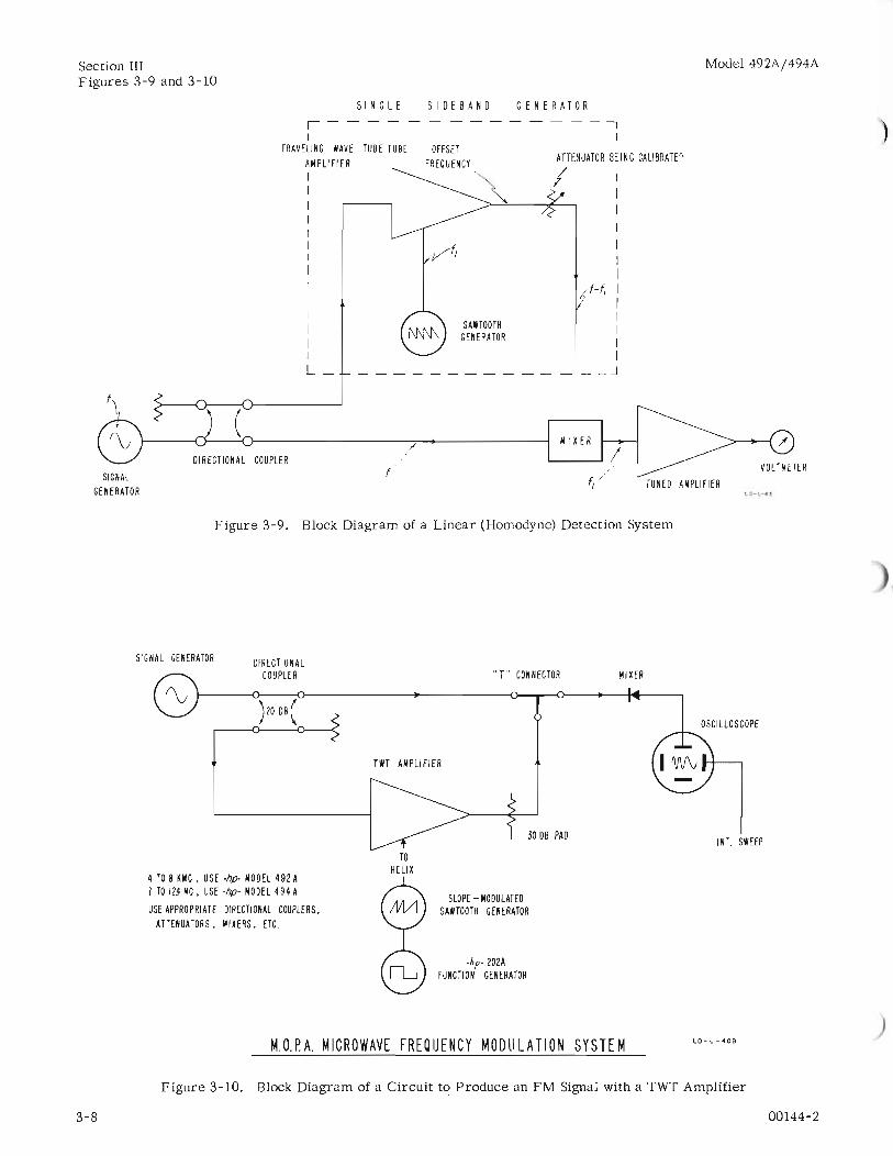
TI ME .. 3-34. HOMODYNE DETECTION.
Figure 3-7. RF Phase Shift Produced byHelix Modulation
3-32. With sawtooth modulation, the desired outputfrequency shift (F in figure 3-8) occurs during thesawtooth formatioJ time, and is proportional to therate of change of voltage. During the sawtooth flyback time the output phase is shifted in the oppositedirection producing an undesired frequency shift (F2in figure 3-8). If the flyback time is made extremelyshort, this frequency is far removed from the desiredfrequency since the degree of frequency shift is inversely proportional to the flyback time. In additionto being far removed from the desired frequency thepower in the undesired frequency is very small sinceit is proportional to the ratio of flyback time to sawtooth time.
3-33. In a typical case involving a desired 50-kc frequency shift, a I-microsecond flyback time wouldproduce a I-megacycle frequency shift in the oppositedirection and would contain only 5% of the total powerin the output wave. In practice, this undesired
3-35. The ability of a twt to produce an offset frequency that is stable with respect to the signal sourcemakes it an ideal instrument to use in a homodyne(linear) detection system. The difference frequencywill be dependent upon the stability of the sawtoothgenerator used to modulate the twt helix, a problemof no consequence at the low modulating frequenciesinvolved.
3-36. A typical linear detector system suitable forcalibrating microwave attenuators is illustrated infigure 3-9. The signal generator supplies a signal(f) both to a crystal mixer and to a traveling wavetube amplifier. The traveling wave tube amplifier issawtooth modulated to produce an offset frequency(f-f ) which is applied to the attenuator to be calibrated. The output signal from the attenuator is thencombined with the original signal (f) in the mixer toproduce a beat frequency (f ) whose amplitude is directly proportional to the ahtplitude of (f-f
j) so long
as the amplitude of (f-fj
) remains within the squarelaw region of the cryStal. This beat frequency isamplified by the tuned amplifier and the output is indicated by an ac voltmeter. The lower sensitivity
01144-2 3-7
Section IIIFigures 3-9 and 3-10
Model 492A/494A
SAWTOOTHGENERATOR
f,
OFFSETFREQUENCY
SINGLE SIDEBAND GENERATOR
-------------1I
ATTENUATOR BE INGCALIBRATE"
/ IIIIIII
f-f, IIIIII
_ _JL_
II
TRAVELING WAVE TUBE TUBEAMPLIFIER
SIGNALGENERATOR
COUPLER /f VOLTMETER
TUNED AMPLIFIERLO-l-'"
Figure 3-9. Block Diagram of a Linear (Homodyne) Detection System
INT. SWEEP
OSCILLOSCOPE
MI XER
30 DB PAO
'T' CONNECTOR
TWT AMPLIFIER
)20 OB (
DIRECTIONALCOUPLER
SIGNAL GENERATOR
4 TO 8 KNC 0 USE -hp- MODEL 492 A7 TO 12.4 MC. USE ·hp· MODEL 494 A
USE APPROPRIATE DIRECTIONAL COUPLERS.ATTENUATORS. MIXERS. ETC.
TOHELIX
SLOPE - MODULATEDSAWTOOTH GENERATOR
.hp' 202AFUNCTION GENERATOR
M.O.P.A. MICROWAVE FREQUENCY MODULATION SYSTEM LD-L-40B
Figure 3-10. Block Diagram of a Circuit tc? Produce an FM Signal with a TWT Amplifier
3-8 00144-2

)
Model 492A/494A
limit is determined by the crystal and IF amplifiernoise and is approximately -100 dbm.
ote
When a swr indicator (such as the <[j) Model4158) calibrated for use with a squarelaw detector is used in place of the tunedamplifier and voltmeter, the db readingsmust be doubled.
3-37. FREQUENCY MODULATION.
3-38. Narrow-band frequency modulation can be obtained by applying the modulation signal directly tothe helix of the twt; however, to frequency modulatewith an appreciable frequency deviation it is firstnecessary to produce an offset frequency as describedin paragraph 3-29. The deviation of the offset frequency should be slightly greater than 1/2 the totalfrequency deviation desired. The offset frequency isthen varied by varying the slope of the sawtooth.
3-39. A sawtooth waveform produced by the specialgenerator described in paragraph 4-20 can be slope-
00144-2
Section 1IIParagraphs 3-37 to 3-40
modulated by any waveform before being applied tothe traveling wave tube helix. In this manner complexsignals can be used to frequency-modulate the signalapplied to the twt and the center of the output frequency will be fixed by the sawtooth repetition ratewithout slope modulation. In no case should the p~ase
shift due to a single sawtooth cycle exceed 360 sothat the amplification properties of the traveling wavetube amplifier will not be adversely affected regardless of the magnitude of the apparent phase deviationwhen the sawtooth wave is modulated.
3-40. Figure 3-10 is a block diagram of a system forthe generation of frequency-modulated offset signals.In this arrangement, the slope-modulated sawtoothvoltage which is applied to the twt helix produces anoffset frequency, the instantaneous frequency of whichis proportional to the slope of the sawtooth. Varyingthe slope of the sawtooth voltage varies the offset frequency. Thus the output signal from the twt is anfm signal. The detected fm signal (the differencebetween the signal generator frequency and the frequency-modulated offset frequency) is shown on theoscilloscope.
3-9

"'", o'r
jC/)
.....
CDO
Qn
c:~.
'i0
CD::s
"'"
,< ......
3:: 8. CD >- "'"'Cl N ;> -.... "'"'Cl "'";>
J4rG
'iiiDl
l!QQJ
J5PIN
JACK
ONFR
ONT
PANE
LFO
RME
ASUR
ING
BIAS
J2
mD
J3
m
(~Jll
HELlX
IMO
O.
Fig
ure
4-1
.B
lock
Dia
gra
m~
Mo
del
s49
2Aan
d49
4A
~
-SR
IHA
LFWA
VERE
CTIF
IER
+
SR2~
VIV5
ASR
3SE
RIES
HELI
XVO
LTAG
ERE
GULA
TOR
MODU
LATO
R
IDO
UBLE
R6B
Q6V4
1126
BQ7A
REFE
RENC
Eew
I-
VOLT
AGE
IHELI
X~
0OA
2ST
RAY
CAPA
CITY
'--c
.--
T1V2
V5B
..,-
,,'-",
CONT
ROL
DISC
HARG
EI
IPO
WER
TUBE
TUBE
,,
I
i~
TRAN
SFOR
MER
6AU6
1 126B
Q7A
IW
I~
II
elY-
:~u
><
@HE
LIXe>
elYI
---
I""
ANOD
E\~.J
~,
"'-
-""~
<
V3~oIGR
IDBI
ASI
<:>BI
ASeIY~
REGU
LATO
ROB
28
0-
L-4
4B
JF1 I.S
A F2 1.6A~
SR4
~T
ITMA
GNET
SISU
PPLY
L----
JL
-
o o ...... "'" "'", N

)
Model 492A/494A
SECTION IV
PRINCIPLES OF OPERATION
Section IVParagraphs 4-1 to 4-13
)
)
4-1. INTRODUCTION.
4-2. The twt amplifier contains very little signal circuitry external to the twt itself. The electrical circuits in the instrument provide the operating voltagesand the means for modulating the twt, as shown in theblock diagram, figure 4-1.
4-3. MAGNET POWER SUPPLY.
4-4. The 492A and 494A utilize a 400-gauss electromagnet (surrounding the traveling wave tube capsule)to hold the emitted electrons in a very narrow beam.The power supply for the magnet consists of a fullwave selenium bridge rectifier connected directlyacross the US-volt line and a capacitive-input filter,and supplies approximately 0.7 ampere at an outputvoltage of 120 volts dc with less than 1 volt rms ripplewhen connected to the magnet. The magnet is coveredby a shield as a protection against stray magneticfields.
4-5. REGULATED POWER SUPPLY.
4-6. The operating voltages applied to the twt areobtained from a voltage doubler followed by a voltageregulator, VI, V2, and V4. The regulation is accomplished by varying the plate resistance of VI in accordance with the output voltage in the following manner, see figure 4-1. V4 is a constant voltage tubewhich holds the voltage at the grid of V2 constant withrespect to the cathode of VI. The cathode of V2 isconnected to a voltage divider between the cathode ofVI and the minus side of the supply. If the cathodevoltage of VI increases, the grid voltage of V2 willalso increase the same amount. However, the cathode voltage of V2 will increase only by an amountequal to the ratio of resistance below the potentiometer arm to the total resistance times the totalvoltage change. Thus, a signal appears on the gridof V2 which is proportional to the rise of voltage onthe cathode of VI. This signal on the grid of V2 isamplified and inverted by V2 and applied to the gridof V1, increasing the plate resistance of V1 and lowering the voltage at the cathode of VI which results ina substantially constant output voltage. If the voltageat the cathode of VI tends to decrease, the plate resistance of VI decreases, holding the voltage at thecathode of V1 substantially constant.
4-7. The chassis Helix control (R25) adjusts the levelof the regulated dc output to compensate for the variations in twt characteristics. The switch, 52, and theassociated voltage dividers permit the use of the samepower supply with two twt types and allows the operator to use the same instrument as a 492A (4-8 gc) oras a 494A (7-12.4 gc) by changing the twt. Changingthe tube type is no more difficult than replacing thetwt with another tube of the same type (see para. 5-17).
00144-2
4-8. The bias voltage for the twt is supplied by V3and controlled by the GRID BIAS control on the frontpanel. The grid of the twt is grounded through a3900-ohm resistor, and the voltage on the cathode isvaried. The circuit is arranged so that all the twtelectrode voltages except the control grid vary as thecathode voltage is varied and therefore remain constant with respect to the twt cathode. If the grid werenot grounded, but connected to a source of variablenegative voltage a blocking capacitor would be requiredwhich would impair the response of the twt to lowfrequency modulating signals. A pin jack on the frontpanel allows the bias voltage to be measured; an external voltmeter haVing 20,000 ohm/volt sensitivity orhigher should be used.
4-9. The anode voltage is controlled by a potentiometer on the chassis of the instrument and is adjustedto obtain normal cathode current for the twt amplifier;see paragraph 5-26. The front panel HELIX controladjusts the helix voltage of the twt to obtain eithermaximum gain and power at a particular frequency oroptimum broadband response.
4-10. TRAVELING WAVE TUBE.
4-11. The basic traveling wave tube consists of anelectron gun which projects a focused electron beamthrough a helically-wound coil to a collector electrode,shown in figure 4-3. The focused electrons are heldin a pin-like beam through the center of the helix bya powerful magnet around the full length of the capsule.
4-12. A cw signal coupled into the input end of thehelix travels around the turns of the helix and thus hasits linear velocity reduced by the amount equal to theratio of the length of wire in the helix to the axiallength of the helix. The electron beam velocity, determined by the potential difference between thecathode and the helix is adjusted so that the electron beamtravels a little faster than the cw signal. The electricfield of the cw signal on the helix interacts with theelectric field created by the electron beam and increases the amplitude of the signal on the helix, thusproducing the desired amplification.
4-13. Figure 4-2 is a diagram showing the principalelements of a typical traveling wave tube in the upperportion and the important steps in the amplificationprocess in the lower portion. The steps should be followed by referring to the numbered captions below.
(1) An electron beam is directed through the centerof the helix.
(2) A cw signal is coupled into the helix. Arrows inthe detail show the direction and magnitude of forceexerted on the electron beam by the cw signal.
4-1

"'"I t-;)
BEAM
FORM
ING
ANOD
E20
0VTO
300
V
,.---
HELIX
MOUN
TING
AND
SHIE
LDVO
LTAG
ESA
NEAS
COLL
ECTO
RLO
SSY
-WIR
E.HE
LIX-C
OUPL
EDAT
TENU
ATOR
COLL
ECTO
RFR
ON50
0V
TO15
00V
(DEP
ENDI
NGON
TUBE
TYPE
l
'TjU
l..
..(1
)O
QO
CM
I-l
....
(1)g
"'".....
.~<
INPU
TDI
RECT
IONA
LCO
UPLE
RSI
NGLE
-WI
REHE
LIXOU
TPUT
DIRE
CTIO
NAL
COUP
LER
CATH
ODE
OV
MODU
LATO
RGR
IDI
OVTO
-50V
TYPE
'N'
INPU
T
!lh I=
IJA
CK--
~
fjjjjjjjjjfjjjjjjjjjjf ril1 I
I
TYPE
'N'
OUTP
UTJA
CK
~ 8. ~ "'"-.0 t-;) » ........ "'"-.0 "'"»
,I
II ,•..
-.n
@----I
Fig
ure
4-2
.T
rav
elin
gW
ave
Tu
be
and
How
ItW
orks
CD
--'\
!\
!~!
..!"
,/1-1
"/1
.>_
.....~~
o o .- "'" "'"I t-;)

Model 492A/494A Section IVFigures 4-3 and 4-4
Figure 4-3. Cutaway View of a Traveling Wave Tube Capsule and Magnet Showingthe Important Elements
OUTPUTCOUPLER
)
COAXIAL CONDUCTOR
CATHODE OUTPUT
Figure 4-4. Cutaway View of an Encapsulated Traveling Wave Tube
00144-2 4-3
Section IVParagraphs 4-14 to 4-21
(3) Electron bunching caused by the electric field ofthe cw signal (see detail).
(4) Amplification of the signal on the helix beginsas the field formed by the electron bunches interactswith the electric field of the cw signal. The newlyformed electron bunch adds a small amount of voltageto the cw signal on the helix. The slightly amplifiedcw signal then produces a denser electron bunch whichin turn adds a still greater voltage to the cw signal,and so on.
(5) Amplification increases as the greater velocityof the electron beam pulls the electron bunches morenearly in phase with the electric field of the cw signal.The additive effect of the two fields exactly in phaseproduces the greatest resultant amplification.
(6) Attenuators placed near the beginning of the helixreduce all the waves traveling along the helix near tozero. This attenuator prevents regeneration andpossible oscillation due to undesired backward waves,such as reflected waves from mismatched loads.
(7) The electron bunches travel through the attenuator unaffected.
(8) The electron bunches emerging from attenuatorinduce a new cw signal on the helix. The new cw signal is the same frequency as the original cw signalapplied.
(9) The field of the newly induced cw signal interacts with the bunched electrons to begin the amplification process over again.
(10) For a short distance the velocity of the electronbunches is reduced slightly due to the large amount ofenergy absorbed by the formation of the new cw signalon the helix.
(11) Amplification increases as the greater velocityof the electron beam pulls the electron bunches morenearly in phase with the electric field of the cw signal.
(12) At the point of the desired amplification theamplified cw signal is coupled out of the helix. Notethat the "amplified" cw signal is a new signal whoseenergy is wholly supplied by the bunched electronbeam.
4-14. The traveling wave tube is completely enclosedin the capsule shown in figure 4-4. The capsule supports and shields the tube and rigidly mounts the capsule attenuator and the input-output couplers, cablesand connectors. The capsule attenuator preventsenergy from being propagated down the capsule in acoaxial mode using the helix as a center conductorand the shield as the outer conductor. The frontpanel INPUT connector connects through a coaxialcable to the helically-wound directional coupler atthegun end of the helix; the OUTPUT connector connectsthrough a similar cable to an identical coupler at thecollector end of the helix. Impedance matching overthe extremely wide frequency range of the twt, isobtained by cavity-coupling. For an explanation of
4-4
Model 492A/494A
cavity-coupling refer to "The Use of Quasi-StaticMode Approximations in the Design of Slow WaveStructure Impedance Matches" by Wayne E. Raub,dated August 1961. Manual number 27-3. Reprintsavailable from Microwave Electronics Laboratory,4061 Transport Street, Palo Alto, California.
4-15. GRID MODULATION.
4-16. The signal being amplified in the traveling wavetube is amplitude-modulated by applying the modulating signal between the cathode and first grid. Makingthe potential on the grid more positive increases thecurrent passing through the center of the helix withoutchanging the velocity and results in greater density ofthe electron bunches which in turn contribute moreenergy to the rf wave being amplified on the helix,and correspondingly increases the level of the outputsignal. Conversely, making the grid more negativedecreases the rf output.
4-17. HELIX MODULATION.
4-18. The Helix Modulator, V5A, is a cathode followerconnected between the regulated voltage and the helix.The front panel HELIX control varies the bias on V5A,and hence the voltage applied to the helix. When thetwt amplifier is helix-modulated, the modulating signal is connected to the grid of the helix modulatorfrom the front panel BNC connector labeled HELIXMOD.
4-19. The rf signal on the helix is phase-modulatedby superimposing the modulating signal on the normaldc helix voltage. Changing the helix voltage changesthe velocity of the electrons in the beam through thehelix without changing beam density. A negative voltage slows the beam down and retards the phase of theoutput signal; a positive voltage speeds up the beam andadvances the phase. Since the final signal taken fromthe helix is the result of electron bunching in the beam,altering the velocity of beam alters the relative positionof the bunches and results in a phase shift between theinput and output signals.
4-20. Since the amount of energy transferred fromthe electron beam to the wave on the helix is in parta function of the phase difference between the fieldsof the helix and the electron bunches, altering theelectron velocity has some effect upon the energygiven to the signal on the helix resulting in some incidental amplitude modulation. Special tubes are available which sacrifice gain to minimize this incidentalamplitude modulation, see paragraph 5-14.
4-21. A certain amount of stray and wiring capacityexists between the helix of the twt and chassis whichmust be charged and discharged as the helix is modulated. When the helix modulating signal goes positivethis capacity can be charged very rapidly through thelow impedance of the helix modulator tube, V5A, andthe power supply. However, if the modulating signalwere a fast negative-going signal, V5A could be cutoff and the stray capacity would discharge through theinsulation (leakage) resistance which exists betweenthe helix and the chassis. This is a relatively long
01144-2

Model 492A/494A Section IVParagraphs 4-22 to 4-25
)
time constant circuit. The discharge tube, V5B, isconnected between the helix of the twt and chassis toform a low-impedance and therefore a rapid-dischargecircuit for this capacity. A negative-going modulatingsignal applied to the HELIX MOD. is coupled to thehelix through the cathode follower, V5A, and simultaneously inverted by V5A and applied to the grid ofV5B. The stray capacity is thus able to dischargerapidly through V5B, allowing a rapid decay timewhen fast pulses are applied to the HELIX MOD. jack.
4-22. CONSTANT-AMPLITUDE, LINEAR SAW-TOOTH GENERATOR.
4-23. To shift the phase or frequency of the rf signalin a traveling wave tube amplifier, a sawtooth suchas is used in oscilloscope sweep circuits can beapplied to the traveling wave tube helix. If the rf output signal is to be a nearly pure offset frequency andcontain a minimum of spurious components, the sawtooth waveform applied to the helix must be constantin amplitude, must be linear, must not contain noiseor ripple and must have a fast flyback time. In addition to frequency-modulate an rf signal, the sawtooth
amplitude and the sawtooth repetition rate must becompletely independent and separately adjustable andthe repetition rate should be adjustable over a widerange. To frequency-modulate an rf signal with atraveling wave tube amplifier it is necessary to modulate the slope or repetition rate of the sawtooth wavewithout affecting the sawtooth amplitude.
4-24. A sawtooth generator having these characteristics is shown in simplified form in figure 4-5.This generator consists of an adjustable, regulatedpower supply, a charging capacitor, a blocking oscillator to charge the capacitor, a pentode tube to discharge the capacitor, and a cathode follower to isolatethe generator from the output.
4-25. The broken line in figure 4-5 indicates thecapacitor-charging circuit, the solid line the dischargecircuit. When power is applied to the generator, thegrid bias on the blocking oscillator tube is zero andthe oscillator goes through one cycle of operation.During the oscillation cycle, the tube conducts heavilyand rapidly charges the capacitor to the B+ voltage,
t----@SAWTOOTH
OUTPUT
SAWTOOTHSLOPE
CD PENTODE DISCHARGESCAPACITOR AT A RATEDETER~INED BY GRIDBIAS
-I-----4~t------@
SLOPEMODULATION
INPUT
o VOLTS
B+r-----I ~ CD BLOCKING OSCILLATOR
;I CHARGES CAPACITORI RAPIDLY TO THE BtI VOLTAGE
II IIII
VARIABLE BtADJUSTS +A~PLI TUDEOF OUTPUTSAWTOOTH
B- ... ......-----4....--------JL 0- L-41
Figure 4-5. Simplified Circuit of a Constant Amplitude, Variable Slope Sawtooth Generator
00144-2 4-5

Section IVParagraphs 4-25 to 4-27
producing a rapid flyback. The charge on the capacitor biases the blocking oscillator tube beyond cutoffand prevents further operation until the charge isremoved.
4-26. The instant the blocking oscillator is biased tocutoff, the capacitor begins to discharge through thepentode tube at a rate determined by the grid bias.The capacitor is discharged at a linear rate due to theconstant current characteristic of the pentode and thusproduces an output voltage with a linear slope. As thecapacitor is discharged, the grid bias on the blockingoscillator returns toward cutoff and at some value the
4-6
Model 492A/494A
tube conducts sufficiently to start the blocking oscillator on another cycle of operation, thus again recharging the capacitor.
4-27. The amplitude of the output sawtooth waveformis adjusted by changing the regulated B+ to vary thecharge placed on the capacitor. The repetition rateor slope is adjusted by changing the pentode grid biasto control the rate at which the capacitor is discharged.Modulating signals applied to the control grid of thepentode modify the nominal grid bias level and changethe capacitors discharge rate, and in turn, the sawtooth slope and repetition rate.
00144-2

)
Mcx:lel 492A/494A
SECTION V
MAINTENANCE
Section VParagraphs 5-1 to 5-6
5-1. INTRODUCTION.
5-2. This section provides maintenance and serviceinformation for Mcx:lels 492A and 494A Traveling WaveTube Amplifiers. The section includes replacementprocedures for tubes, recommended test equipment,adjustment procedures, and troubleshooting. Thissection also includes performance checks which verify proper instrument operation.
5-3. CLEANING THE AIR FILTER.
5-4. Inspect the air filter regularly, and clean itbefore it becomes dirty enough to restrict air flow.
a. Remove filter from instrument rear, and washit in warm water and detergent.
b. Dry filter thoroughly and coat it with filter adhesive. We recommend Filter Coat No.3 from Research Prcx:lucts Company, Inc. This adhesive comesin "Handi-Koter" sprayer cans and is available frommost heating supply stores or from your authorizedHewlett-Packard sales representative.
5-5. TEST EQUIPMENT.
5-6. Test equipment recommended for use in maintaining and checking performance of the Mcx:le1s 492Aand 494A is listed in table 5-1. Equipment havingsimilar characteristics can be substituted for theequipment listed.
)
)
Table 5-1. Recommended Test Equipment
Instrument Type Required Characteristics Use Mcx:lel
AC Voltmeter Voltage Range: 1.0 mv to 1 volt Power supply ripple ~ Mcx:lel 4000Voltage Accuracy: 2% Spurious mcx:lulation checkInput Impedance: 10 megohoms
DC Voltmeter/ Voltage Range: to 1000 volts Power supply ~ Mcx:lel 4108Ohmmeter Voltage Accuracy: 3% measurements
Imput Impedance: 100 megohms
Crystal Detector Frequency Range: to 12.4 gc Spurious mcx:lu1ation check ~ Mcx:lel 420ASensitivity: approximately 0.1 V/mw
Power Meter Power Range: up to 10 mw Gain check ~ Model 430CScale must read in dbm and milliwatts Power check
Noise figure check
DC Voltage Division ratio: 100: 1 or 3: 1 Power supply ~ Mcx:lel 459ADivider Input Impedance: 12,000 megohms measurements
Maximum Voltage: 2000 volts
Thermistor Mount Power Range: to 10 mw Gain check ~ Mcx:lel 4778Frequency Range: to 10 gc Power check
Noise figure check
Signal Generator Frequency Range: 4 to 12.4 gc Power source for ~ Mcx:lels 6188Output Amplitude: at least 1 mw performance checks 620A,626A
Waveguide Coax SWR less than 1.25 With all checks at 10 gc ~ Mcx:lel X281AAdapter and above
Waveguide Power Range: to 10 mw Gain check ~ Mcx:lel X4878Thermistor Mount Frequency Range: to 12.4 gc Power check
Attenuator 10 db power attenuation Power check Weinschel 210-10
00144-2 5-1

Section VFigure 5-1
Model 492A/494A
SR4----....:;:;..=
S2----f--=-.:::::.!
C2
C1
RT1----...;...:,,...;-d~.:
SR2-----;:'
SR3----
~~-'i..:.-...,---MEASU RE TWl
1t:;~~~~}__~H~E:A~T:E:R VOLTAGE~ R47
ir------- C8
r-----r.14
C3A/BV3
~~5.-----V4
---7-r---';O',.....--------C 10
MP-S-5558
Figure 5-1. Top View of Models 492A and 494A
00144-2

)
Model 492A/494A
5-1. REPAIR.
5-8. CABINET REMOVAL.
5-9. To remove the instrument chassis from thecabinet proceed as follows:
a. Place the twt panel down on a soft pad.
b. Remove the two 10-32 round head machinescrews which secure the rear of the cabinet to the instrument chassis.
c. Lift the cabinet up and off the chassis. Thepanel bezel remains attached to the panel.
5-10. TUBE REPLACEMENT.
5-11. A list of tubes in the 492A and 494A and thechecks and adjustments that must be made followingreplacement, are in table 5-2.
Table 5-2. Tube Replacement List
Tube Function AdjustmentType
VI Series Regulator Check voltage rangeof HELIX control(see sChematic)
Adj. R25 if necessarysee paragraph 5-24.
V2 Control Tube Same as VI.
V3 Bias Regulator Check range of GRIDBIAS control.
V4 Reference Tube Same as VI.
V5A, a. Helix Modulator Same as VI.B b. Discharge Tube
V6 Traveling Wave Tube See para. 5-12.
5-12. TRAVELING WAVE TUBE CAPSULEREPLACEMENT.
5-13. Because the traveling wave tube is fragile andadjustment of the coupling helices is critical, replacement tubes are furnished in the complete capsule assembly which includes the tube, coupling helices, coaxial cables, and panel connectors completein a single unit. Refer to the "Conditions of Warranty" page in the manual.
5-14. Special traveling wave tubes in which gain hasbeen sacrificed to obtain a more constant output overthe full frequency range and a very low value of incidental amplitude modulation during phase modulationare available on special order.
5-15. REMOVAL. To remove the encapsulatedtraveling wave tube from the 492A or 494A proceedas follows:
00144-2
Section VParagraphs 5-7 to 5-16
a. Remove the instrument from the cabinet. (Seeparagraph 5-8.)
b. Disconnect the twt collector lead connector atthe rear of the capsule, shown in figure 5-3.
c. Remove the screws mounting the INPUT andOUTPUT connectors to the panel.
d. Loosen all the capsule alignment screws. Thefront alignment screws are shown in figure 5-2 andthe rear alignment screws are shown in figure 5-3.
e. Remove twt plug from socket. This plug islocated on bottom of instrument. Refer to figure 5-2.Grasp the rear of the capsule and carefully pull it outof the magnet.
5-16. INSTALLATION AND ALIGNMENT. To installand align a traveling wave tube capsule proceed asfollows:
a. Hold the twt capsule so the recessed hole incollar is turned upward; insert the capsule into themagnet and be sure the spring-loaded ball (bulletcatch) seats into the recessed hole.
b. Plug the collector lead into its connector asshown in figure 5-3.
c. Reconnect twt plug to socket as shown in figure 5-2.
d. Turn the GRID BIAS control completely clockwise for the most negative bias voltage (cathode positive); turn the power ON. If necessary adjust R47 toobtain correct heater VOltage. Refer to twtdata sheet(supplied with new tubes) and figure 5-1.
e. The alignment screws determine the position ofthe capsule in the magnet. When the capsule is correctly positioned the helix current will be minimum(near zero). Therefore the relative level of the current flowing in the helix is an indication of correctcapsule positioning.
f. Set meter switch to HELIX. If the meter indication is near zero, there is insufficient current flowto check the alignment. Reduce the grid bias voltageuntil the meter indicates some small readable helixcurrent; at the same time be sure that the cathodecurrent is below its safe maximum for continuousoperation after warmup, see table 3-1.
g. Adjust the alignment screws to the setting whichminimizes the helix current.
h. Reduce the cathode current with the anode control and turn the GRID BIAS control to 0, then adjustthe anode control to obtain the normal cathode current(see the meter plate that came with the new tube).
i. Readjust the alignment screws; note the electrode currents. If any currents are abnormal seeparagraph 5-30.
j. Lock the alignment screws, at the same timewatching the meter to see that the helix current doesnot increase. Note the meter reading.
5-3

Section VFigures 5-2 and 5-3
INPUTRF CABLE
FRONTALIGNMENTSCREW
Model 492A/494A
PLUG
,'""==----;:!!I--- 0 UTPUTRF CABLE
FRONTALIGNMENTSCREW
Figure 5-2. Bottom View Looking Towards the Front Panel of Models 492A and 494A
REARALIGNMENTSCREW
INPUT _----,RF" CABLE
COLLECTORLEAD
TWT CAPSULE
MP-S-I020
REARALIGNMENTSCREW
5-4
Figure 5-3. Rear View of Models 492A and 494A
00144-2

)
Model 492A/494A
k. Remove the meter plate which indicates thenormal cathode current for the old tube and installthe new plate.
m. Perform the chassis Helix control adjustment,see paragraph 5-24.
n. Turn the power off and install the cabinet.
p. Set the meter switch to HELIX and turn thepower ON. The meter reading should be the same asin step j; if not, the setting of the capsule was disturbed when the cabinet was replaced. Turn off thepower, remove the cabinet, and reposition the capsuleas before, starting with step f. Replace cabinet; againmeasure the cathode and helix currents, which shouldbe the same as with cabinet removed.
5-17. CHANGI G THE FREQUENCY RANGE OFTHE492A OR 494A.
5-18. The t$j) Models 492A and 494A are identical except for the traveling wave tube type supplied and theoperating voltage adjustments. The proper range ofdc operating voltages for one tube type or the other isselected by S2 on the instrument chassis (figure 5-1).
5-19. To change a 492A to a 494A proceed as follows:
a. Remove the cabinet; see paragraph 5-8.
b. Remove the twt capsule; see paragraph 5-15.
c. Turn S2 to the 494A position; see figure 5-1.
d. Install the typeM2201-K(HPI952-0009)installation procedure is the same as type M2207-A exceptS2 should be in 494A position. (See paragraph 5-16.)
5-20. To change a 494A to a 492A proceed as follows:
a. Remove the cabinet; see paragraph 5-8.
b. Remove the twt capsule; see paragraph 5-15.
c. Turn S2 to the 492A position, see figure 5-1.
d. Install the typeM2207-A (HPI952-0012) installation procedure is the same as type M2201-K, exceptS2 should be in 492A position. (See paragraph 5-16.)
5-21. ADJUSTMENTS.
5-22. EXCESSIVE HELIX CURRENT.
5-23. If excessive helix current is indicated on thefront panel meter with normal currents in the othertwt electrodes, the electron beam is not being focusedaccurately through the center of the helix. Measurethe dc voltage and current supplied to the magnet at115 volt line, which should be approximately 120 voltsat 700 mao The ac ripple on the magnet supply shouldbe less than 1 volt rms. If these measurements donot reveal the cause of the trouble, check the alignment of the twt in the magnet. See paragraph 5-16.
00144-2
Section VParagraphs 5-23 to 5-29
5-24. CHASSIS HELIX CONTROL.
5-25. The chassis Helix control, R25, determinesthe range of the front panel HELIX control by governing the output voltage of the regulated power supply.This adjustment should be performed whenever a newtwt capsule is installed or the gain of the amplifier isless than 30 db. To adjust, proceed as follows:
a. Remove the cabinet, see paragraph 5-8.
b. Set twt HELIX control to position 5, and adjustGRID BIAS control to obtain normal cathode current.
c. Connect a test setup as shown in figure 5-4.
d. Set the generator for the Model 492A to 4 gc,for the Model 494A to 7 gc. For both models set thegenerator attenuator to -30 dbm, in cw operation.
e. Adjust the chassis Helix control, R25, for maximum gain, as read on the 430C.
f. Change the frequency of the generator, for theModel 492A to 8 gc, for the Model 494A to 12.4 gc,maintaining the same power level.
g. The 430C should read greater than 0 dbm. Ifthe 430C doesn't read greater than 0 dbm, readjustthe chassis Helix control, R25, to obtain from 0 dbmto +2 dbm. Recheck the gain for the Model 492A at4 gc, for the Model 494A at 7 gc, and readjust R25,if necessary, to obtain nearly equal gain at both frequencies.
5-26. ANODE VOLTAGE CO TROL.
5-27. The Anode control, R30, on the chassis of theinstrument, (see figure 5-1), is provided so that thetwo cathode current can be maintained at its normallevel (as indicated on the plate attached to the meterface) as the tube ages. To adjust proceed as follows:
a. Place meter selector switch to CATH. positionand GRID BIAS control to O.
b. Rotate Anode control adjust, R30, to obtainnormal cathode current. Also note that other tubeelement currents do not exceed their safe maximumlimits (see table 3-1).
5-28. REGULATED POWER SUPPLY.
5-29. To check the regulated power supply, proceedas follows:
a. Set GRID BIAS control to O.
b. Connect a dc voltmeter to the output of thepower supply, at pin 3 of VI.
c. Adjust the line voltage from low to high line(103 - 127 volts). Power supply voltage should notchange more than 10 volts.
5-5

Section VParagraphs 5-30 to 5-31
d. Connect an ac voltmeter to the output of thepower supply, at pin 3 of VI.
e. Adjust the line voltage from low to high line(103 - 127 volts). Ripple voltage should not begreater than 7 mv.
5-30. TROUBLESHOOTING.
5-31. If the twt amplifier is suspected of unsatisfactory operation, proceed as follows:
Model 492A/494A
a. Remove all the external connections to the instrument and set GRID BIAS to zero.
b. Measure the electrode currents of the twt usingthe front panel meter.
c. If the electrode currents are abnormal, removethe instrument from the cabinet (see paragraph 5-8)and with the indication observed, determine thepossible cause and action from table 5-3.
Table 5-3. Troubleshooting Chart
Indication Possible Cause Action Check
Cathode current low Regulated voltage low Replace VI Table 5-2Check regulation Para. 5-28
Low or no helix voltage Replace V5 Table 5-2
Low anode voltage Adjust anode voltage Para. 5-26
Low twt emission Replace capsule Para. 5-12
Cathode current high High anode VOltage Adjust anode voltage Para. 5-26
Gassy twt Replace capsule Para. 5-12
Anode current high Low helix voltage Adjust chassis helix voltage Para. 5-24Replace V5 Table 5-2
Gassy twt Replace capsule Para. 5-12
High anode voltage Adjust anode voltage Para. 5-26
Helix current high Misalignment of the twt Align capsule Para. 5-16
Collector current Low, or no twt magnet current Replace F2 (iffan does not turn)low (low field). Replace defective magnet powersupply components.
No voltage on collector (discon-nected at connector), Fig. 5-3
No or little control of High impedance path between the Replace capsule Para. 5-12Cathode current with anode and grid. May be 40 meg-GRID BIAS control. ohms or more.
Low gain. Misadjustment of anode voltage. Adjust anode VOltage Para. 5-26The anode may have been ad-justed to obtain the COrrectcathode current with some gridbias on the tube.
Wrong value of helix voltage Adjust chassis helix voltage Para. 5-24
Low cathode current See cathode current low(in indication column)
Oscillation Defective Helical Attenuator Replace capsule Para. 5-12
Excessive cathode current See cathode current high(in indication column)
5-6 00144-2
Model 492Aj494A Section IParagraphs 5-32 to 5-44
5-32. PERFORMANCE CHECKS.
5-33. GAl CHECK.
5-34. For Model 492A proceed as follows:
d. Set the two HELIX control to position 5, andposition the GRID BIAS control to full counterclockwise.
e. Adjust the output power of the generator untilthe 430C reads 2 miIIiwatts.
a. Set the twt HELIX control to position 5, andposition the GRID BIAS control to full counterclockwise. f. Repeat steps c through e throughout the fre
quency band of the twt amplifier, up to 8 gc.
b. Connect test set up as shown in figure 5-4.
c. Set the generator attenuator to -30 dbm, witha frequency output of 4 gc, in cw operation.
d. The 430C should read greater than 0 dbm.
5-38. For Model 494A as for Model 492A, except,generator to be used in figure 5-4 to have a frequencyrange from 7 to 12.4 gc, and the test should start at7 gc and end at 12.4 gc.
e. Change the frequency of the generator to 8 gc,maintaining the same power level. 5-39. NOISE FIGURE CHECK.
f. The 430C should read greater than 0 dbm. 5-40. For Model 492A proceed as follows:
a. Connect test set up as shown in figure 5-4.
5-35. For Model 494A proceed as for Model 492A,except, generator to be used in figure 5-4 to have afrequency range from 7 to 12.4 gc, and the test shouldbe made at these frequencies.
b. Set generator to 6 gc, in cw operation.
c. With generator output power turned off, adjustthe twt HELIX control for a maximum dbm indicationon the 43OC. Record this reading.
5-36. OUTPUT POWER CHECK.
5-37. For Model 492A proceed as follows:
a. Connect test set up as shown in figure 5-4 andinsert a 10 db attenuator between the twt amplifierand the 477B Thermistor Mount.
b. Set the 430C to the 3 mw range.
c. Set the generator to a frequency output of 4 gc,in cw operation.
d. With generator output power turned on, adjustthe generator attenuator to obtain a reading on the430C that is 3 db greater than that recorded in step c.
e. Record the reading on the generator attenuatordial.
f. Take the reading obtained in step e and subtract it from -78 dbm, for the Model 492A. The result is the noise figure for this 492A.
~MODEL430CPOWER METER
~MODEL492A/494ATWT AMPLIFIER
~MODEL6188/620A!626ASIGNAL GENERATOR §] rg©
Mo!l© ©© a © 4778
THERMISTORMOUNT
~
0 (0INPUT OUTPUT
RF OUTPUT ( 0 0RO
)
MODELX281A
ADAPTER
MODELX4878THERMISTOR
TO REPLACE 477BAT FREQUENCIESABOVE IOGC.
Figure 5-4. Test Setup for Gain, Output Power, and Noise Figure Performance Checks
00144-2 5-7

Section VParagraphs 5-41 to 5-44
~DEL618B/620A/
~DEL492A/494ATWT AMPLIFIER
Model 492A/494A
~DEL4000VACUUM TUBE VM
626ASIGNAL GENERATOR §] g@ !DEV~© ©
© a co 420ACRYSTAL
DETECTOR =(()
~rOUTPuT
INPUT ouTPUT (8)RF OUTPUT (
RO
Figure 5-5. Test Setup for Hum and Spurious Modulation Performance Check
5-41. For Model 494A proceed as for Model 492A,except, the generator to be used in figure 5-4 is tobe set at a frequency of 9.7 gc. The value from whichthe attenuator dial reading is to be subtracted, is-76.7 dbm for the Model 494A.
5-42. HUM AND SPURIOUS MOOULATIO CHECK.
5-43. For Model 492A proceed as follows:
a. Connect test setup as shown in figure 5-5.
b. Set the generator to 8 gc and to square wavemodulation, 1000 pps.
5-8
c. Set the twt HELIX control to position 5, andposition the GRID BIAS control to full counterclockwise.
d. Adjust the generator attenuator until the outputis indicated as a -20 db on the 4000.
e. Switch the generator to cw operation.
f. Record the reading on the 4000.
g. Take the difference, in db's, in the readingsin steps d and f and add to it 8 db. The sum ofthese two numbers should be greater than 45 db.
5-44. For Model 494A proceed as for Model 492A,except, the generator to be used in figure 5-5 is tobe set at a frequency of 12.4 gc.
00144-2

8 ......
>I>
>l>
I N
J'
Io~
"4
1~
10
0.
~ 8. CD ..... >I>
'0 N > ' >I>
'0 >I> >
-II
++--IZOY~
:--~--~
IM
...G
NE
TI
~----
I
.. [!;!
!]~
Slo
·eLO
lUC
K
J1 OPAl.
V6
1952
-001
2(4
92
A)
19
52
-00
09
(49
4A
)
TWT
~=
IOU7PV
TI
J>
o1"
·PU
TI
W~--
=~
JSP
INJA
CK
ON
PA
NE
LFO
RM
EA
SU
RIN
GliA
S
l..m
1r-
OO
ZlJ
.FR
44
.3
.9k
CI.
2O~'
~ IS3""'-:.~_
_!3!~"1
-JV
V\r-
'.0 '0
'CA
TH
OD
EI
'00
3301
<... 3301
(C
13
...L
O.I
IJ,-
-r
so
ICO
LL
EC
TO
R'
~'.
OO
E
IIH
EL
IX'
'.Hoo
d...
CW
(AO
J.FO
RM
AX
.CA
THC
UR
)
<2~~
~T
.0<;>
NO
TE
Sl
DC
VO
LTA
GE
SM
EA
SU
RE
DF
RO
MC
HA
SS
ISW
ITH
VT
VM
.G
RID
BIA
SS
ET
TOZ
ER
O.
CH"'$SIS~
CO
NT
RO
LS
ET
TOC
EN
TE
R,
II'V
OLT
•6
0I'
\;L
INE
.V
OL
TA
GE
SA
DJU
ST
ED
FOR
IND
IVID
UA
LV
6,
LIM
ITS
MA
YV
AR
Y:t
,OW
LT
S.
2.U
ND
ER
LIN
ED
VO
LTA
GE
SA
RE
FOR
hp
MO
DE
L4
94
A.
...V
OL
TA
CE
RA
NC
EW
HE
NF
RO
NT
PA
NE
LH
ELI
X,
A21
,IS
VA
RIE
DB
ET
WE
EN
LIM
ITS
•V
OL
TA
CE
RA
NG
EW
HE
NC
HA
SS
ISH
ELI
XC
ON
TR
OL,
RlS
,IS
VA
RIE
DB
ET
WE
EN
LIM
ITS
1.R
ES
IST
AN
CE
INQ
HM
SU
NLE
SS
OT
HE
RW
ISE
NO
TE
D
4W
HE
NR
EP
LAC
ING
V6
,A
DJU
STill
AS
RE
QU
IRE
DTO
OB
TA
INT
HE
CO
RR
EC
TH
EA
TE
RV
OLT
AG
EFO
Rv6
.5
HE
AV
Y9
0X
IND
ICA
TE
SFR
ON
TP
AN
EL
EN
GR
AV
ING
.
... '.OK
••• ,"".
V3
C.-
l'''f
OB
2.047~f
SOl(
cw
BIAS
-."~
RECU
LATO
R1'
12B
IAS
27.
-.,.
l..c
oC
7..
.L(j)
r-.2'~'
,0·~·T
." ,.. .,. ,.. ." ,.. t-.16 ". "7 ,.. .,. ,.. ." ,.. "0 ,..
CO
f'Y
lIG
HlI'~
IYH
lWlm
PA
Clt
AiD
CO
/llU
'AN
T
lhlo
....
wl.
.,I.
"'•
•IOl
I...
,..
1h••
_..
Ie..
....
._
.".,
,__
.1""
wi."
••do~
....
'.O
MII
,...
••,.
...1
__
,.1,...
H..
.'"'
"~
c.,
,.,.
1__
vo
'(jJ
AM
PE
RIT
E0
-•
1I
C2
'SIH
~l~'
...,
YEL
LOW
C,00
\1'
51
.%
-51
8l2
1J
IPO
WE
.j ., I.'.S
LO
-8L
O
,r--
----
-...~
P';
;/
/
CJ1 I '0 ' CJ1 I ...... o
Fig
ure
5-6
.M
odel
s49
2Aan
d49
4AT
rav
elin
g-W
ave
Am
pli
fier
s
'T1 ....
UJ
oqCD
Cn
"1M
CD..
.. oC
J1::
l
6-<

Model 492Aj494A Section VIParagraphs 6-1 to 6-7
) SECTION VI
REPLACEABLE PARTS
6-1. INTRODUCTION. 6-4. ORDERING INFORMATION.
6-2. This section contains information for orderingreplacement parts. Table 6-1 lists parts in alphanumerical order of their reference designators andindicates the description and ~ stock number of eachpart, together with any applicable notes. Table 6-2lists parts in alpha-numerical order of their ~ stocknumbers and provides the following information oneach part:
6-5. To order a replacement part, address order orinquiry either to your authorized Hewlett-Packardsales representative or to
CUSTOMER SERVICEHewlett-Packard Company395 Page Mill RoadPalo Alto, California
a. Description of the part (see list of abbreviationsbelow).
b. Manufacturer of the part in a five-digit code;see list of manufacturers in appendix.
c. Typical manufacturer's stock number.
d. Total quantity used in the instrument (TQ column).
e. Recommended spare part quantity for completemaintenance during one year of isolated service(RS column).
6-3. Miscellaneous parts not indexed in table 6-1 arelisted at the end of table 6-2.
or, in Western Europe, to
Hewlett-Packard S.A.Rue du Vieux Billard o. 1Geneva, Switzerland.
6-6. Specify the following information for each part:
a. Model and complete serial number of instrument.
b. Hewlett-Packard stock number.
c. Circuit reference designator.
d. Description.
6-7. To order a part not listed in tables 6-1 and 6-2,give a complete description of the part and include itsfunction and location.
ABCCRDLDSE
= assembly= motor= capacitor= diode= delay line= device signaling (lamp)= misc electronic part
FFLJKLM
= fuse= filter= jack= relay= inductor= meter
REFERENCE DESIGNATORS
P = plugQ = transistorR = resistorRT = thermistorS = switchT = transformer
v = vacuum tube, neonbulb, photocell, etc.
W = cableX = socketXF = fuseholderXV = tube socketXDS = lampholder
~ = bandpassbwo = backward wave
oscillator
c = carboncer = ceramiccmo = cabinet mount onlycoef = coefficientcom = commoncomp = compositionconn = connectioncrt = cathode - ray tube
lin = linear taperlog = logarithmic taper
m = milli = 10- 3M = megohmsrna = milliamperesminat= miniaturemfg = metal film on
glassmfr = manufacturer
ABBREVIATIONS
mtg = mountingmy = mylar
td = time delayTi0
2= titanium dioxide
tog = toggletol = tolerancetrim = trimmertwt = traveling wave tube
var = variablewi = withW = wattsww = wirewoundwlo = without
• = optimum valueselected at factory,average valueshown (part maybe omitted)
rot = rotaryrms = root- mean- squarermo = rack mount only
s- b = slow - blowSe = seleniumsect = section( s)Si = siliconsl = slide
= normally closed= neon= normally open= negative positive
zero-zero temperature coeffic ient
= not separatelyreplaceable
nsr
obd = order by de-scription
p = peakpc = printed circuit
boardpf = picofarads =
10- 12 faradspp = peak- to- peakpiv = peak inverse
voltagepos = position(s)poly = polystyrenepot = potentiometer
rect = rectifier
NCNeNONPO
elect = electrolyticencap= encapsulated
impg = impregnatedincd = incandescentins = insulation ( ed)
h = henriesHg = mercury
Ge = germaniumgrd = ground (ed)
K = kilo
f = faradsfxd = fixed
= deposited= detector
= Tubes and transistorsselected for bestperformance will besupplied if orderedby ~ stock numbers;tubes or transistorsmeeting ElectronicIndustries' Association standards willnormally result ininstrument operatingwithin specifications
EIA
delidet
co,....0>0-<0-<o
00144-2 6-1

Section VITable 6-1
Table 6-1. Reference Designation Index
Model 492A/494A
Circuit~ stock No. Description If Note
ReferenceB1 3140-0010 Motor, AC
B1A 3160-0014 Fan blade
C1, 2 0180-0025 fxd, elect, 4 sect, 20 j.L f/sect, 450 vdcw
C3AB 0180-0012 fxd, elect, 2 sect, 20 jJf/sect, 450 vdcw
C4, 5 0160-0082 fxd, paper, 4 j.Lf ±1O%, 1000 vdcw
C6 0160-0097 fxd, paper, 0.25 j.Lf ±1O%, 2000 vdcw
C7 0160-0037 fxd, paper, 0.04 j.Lf ±20%, 1600 vdcw
C8, 9 0160-0005 fxd, paper, 0.047 j.Lf ±10%, 600 vdcw
C10 0160-0037 fxd, paper, 0.04 j.Lf ±20%, 1600 vdcw
C11 0150-0023 fxd, cer, 0.002 j.Lf ±20%, 1000 vdcw
C12 0160-0040 fxd, paper, 0.01 j.Lf ±1O%, 1000 vdcw
C13 0160-0001 fxd, paper, 0.1 j.Lf ±10%, 600 vdcw
C14 0180-0011 fxd, elect, 20 j.Lf, 450 vdcw
C15 490A-82 Cathode Bypass Assembly: O. 002 j.Lf
DS1 2140-0009 Lamp, incd: 6-BV, O. 15 amp, #47
F1, 2 2110-0005 Fuse, cartridge: 1.6 amp s-b
J1 1250-0083 Connector, BNC: female
J2,3 nsr; part of V6
J4 1250-0083 Connector, BNC: female
J5 1251-0073 Jack, telephone tip: for single conductor
J6 1251-0027 Connector, female
L1 9110-0019 Choke: 1 H
M1 1120-0060 Meter: ammeter
P1 8120-0015 Power cable
P2 thru P5 Not Assigned
R1 0690-2231 fxd, comp, 22K ohms ±10%, 1 W
R2 0693-4731 fxd, comp, 47K ohms ±10%, 2 W
R3 0690-4701 fxd, comp, 47 ohms ±10%, 1 W
R4 0690-3941 fxd, comp, 390K ohms ±1O%, 1 W
R5 0690-3341 fxd, comp, 330K ohms ±10%, 1 W
R6 0690-8251 fxd, comp, 8. 2M ±1O%, 1 W
R7 0690-2251 fxd, comp, 2. 2M ±1O%, 1 W
R8 0690-1521 fxd, comp, 1500 ohms ±10%, 1 W
R9 0690-3941 fxd, comp, 390K ohms ±10%, 1 W
R10 0687-1051 fxd, comp, 1M ±10%, 1/2 W
R11 2100-0044 var, comp, lin, 50K ohms ±10%
R12 0690-2731 fxd, comp, 27K ohms ±10%, 1 W
# See introduction to this section
6-2 00144-2

Model 492A/494A Section VITable 6-1
Table 6-l. Reference Designation Index (Cont'd)
Circuit<FiJ stock No. Description* Note
ReferenceR13, 14, 15 0693-1831 fxd, comp, 18K ohms ±10%, 2 W
R16, 17 0693-1531 fxd , comp, 15K ohms ±10%, 2 W
R18, 19, 20 0693-1831 fxd , comp, 18K ohms ±10%, 2 W
R21 0693-2241 fxd, comp, 220K ohms ±1O%, 2 W
R22 0693-1541 fxd, comp, 150K ohms ±10%, 2 W
R23 0693-1841 fxd, comp, 180K ohms ±1O%, 2 W
R24 0690-6831 fxd, comp, 68K ohms ±10%, 1 W
R25 2100-0044 var1 comp, lin, 50K ohms ±10%
R26 0690-8231 fxd , comp, 82K ohms ±10%, 1 W
R27 2100-0133 var1 comp, 200K ohms ±20%, 2 W
R28 0690-5641 fxd , comp, 560K ohms ±1O%, 1 W
R29 0690-6831 fxd, comp, 68K ohms ±10%, 1 W
R30 2100-0043 var1 comp, lin, 500K ohms ±10%
R31 0690-4721 fxd , comp, 4.7K ohms ±1O%, 1W
R32 0687-1051 fxd, comp, 1M ±10%, 1/2 W
R33 0687-4741 fxd, comp, 470K ohms ±1O%, 1/2 W
R34 0690-6821 fxd, comp, 6800 ohms ±1O%, 1 W
R35, 36 0690-3341 fxd, comp, 330K ohms ±1O%, 1 W
R37 thru R40 492A-26A fxd, ww1 50 ohms
R41 0690-1041 fxd, comp, lOOK ohms ±10%, 1W
" R42, 43 Not Assigned
R44 0690-3921 fxd, comp, 3900 ohms ±10%, 1 W
R45 0693-1211 fxd, comp, 120 ohms ±10%, 2 W
R46 Not Assigned
R47 0693-4701* fxd, comp, 47 ohms ±5%, 2 W
RT1 0852-0003 Ballast tube, Amperite type 6-4
Sl 3101-0003 SWitch, tog: DPST
S2 3100-0055 SWitch, rot: 4 pole, 2 pos
S3 3100-0099 Switch, rot: 1 sect, 4 pos
SR1 1882-0007 Rectifier, metallic: 620 rna
SR2, 3 1880-0007 Rectifier, metallic: 1430 V
SR4 1880-0003 Rectifier, metallic: 130 V
T1 9100-0109 Transformer1 power
V1 1923-0026 Tube, electron: 6BG6
V2 1923-0021 Tube, electron: 6AU6
V3 1940-0007 Tube, electron: OB2
V4 1940-0004 Tube, electron: OA2
)
# See introduction to this section
00144-2 6-3

Section VITable 6-1
Table 6-1. Reference Designation Index (Cont'd)
Model 492A/494A
Circuit r[j> stock No. Description 'if NoteReference
V5 1932-0021 Tube, electron: 6BQ7A
V6 1952-0012 encap TWT, (492A only) includes .12, 3
1952-0009 encap TWT, (494A only) includes .12, 3
MISCELLANEOUS
G-74D Knob: METER SELECTOR switch
G-74N Knob: CATH. COL.
1200-0009 Socket, tube: 7 pin
1200-0020 Socket, tube: octal
1251-0044 Connector: female and male contacts
1400-0084 Fuseholder
1401-0006 Clip, tube: plate and grid, cer, ins
1450-0027 Lamp holder, bayonet type
3150-0005 Filter, air: 6X6"
9161-0005 Solenoid Assembly
'if See introduction to this section
6-4 00144-2

Model 492A/494A
Table 6-2. Replaceable Parts
Section VITable 6-2
)
~stockNo. Description# Mfr. Mfr. Part No. TQ RS
490A-82 Cathode Bypass Assembly: O. 002 Ilf 28480 490A-82 1 1
492A-26A fxd, WW, 50 ohms 28480 492A-26A 4 1
0150-0023 fxd, cer, 0.002 Ilf ±20%, 1000 vdcw 91418 JF.002 1 1
0160-0001 fxd, paper, O. 11lf ±1O%, 600 vdcw 56289 160P10496 1 1
0160-0005 fxd, paper, 0.047 Ilf ±10%, 600 vdcw 56289 160P47390 2 1
0160-0037 fxd, paper, 0.04 Ilf ±20%, 1600 vdcw 14655 ST16S4-20 2 1
0160-0040 fxd, paper, O. 011lf ±1O%, 1000 vdcw 14655 TST-100 1 1
0160-0082 fxd, paper, 4 Ilf ±1O%, 1000 vdcw 00656 JP09 2 1
0160-0097 fxd, paper, 0.25 Ilf ±lO%, 2000 vdcw 00656 2009 1 1
0180-0011 fxd, elect, 20 Ilf, 450 vdcw 56289 D32550 1 1
0180-0012 fxd, elect, 2 sect, 20 Ilf/sect, 450 vdcw 00853 LPI (obd) 1 1
0180-0025 fxd, elect, 4 sect, 20 Ilf/sect, 450 vdcw 56289 D32452 2 1
0687-1051 fxd, comp, 1M ±10%, 1/2 W 01121 EB-1051 2 1
0687-4741 fxd, comp, 470K ohms ±lO%, 1/2 W 01121 EB-4741 1 1
0690-1041 fxd, comp, lOOK ohms ±10%, 1W 01121 GB-1041 1 1
0690-1521 fxd, comp, 8.2M ±lO%, 1 W 01121 GB-1521 1 1
0690-2231 fxd, comp, 22K ohms ±10%, 1 W 01121 GB-2231 1 1
0690-2251 fxd, comp, 2.2M±10%, 1W 01121 GB-2251 1 1
0690-2731 fxd, comp, 27K ohms ±10%, 1 W 01121 GB-2731 1 1
0690-3341 fxd, comp, 330K ohms ±lO%, 1 W 01121 GB-3341 3 1
0690-3921 fxd, comp, 3900 ohms ±1O%, 1 W 01121 GB-3921 1 1
0690-3941 fxd, comp, 390K ohms ±lO%, 1 W 01121 GB-3941 2 1
0690-4701 fxd, comp, 47 ohms ±10%, 1 W 01121 GB-4701 1 1
0690-4721 fxd, comp, 4.7K ohms ±10%, 1 W 01121 GB-4721 1 1
0690-5641 fxd, comp, 560K ohms ±1O%, 1 W 01121 GB-5641 1 1
0690-6821 fxd, comp, 6800 ohms ±1O%, 1 W 01121 GB-6821 1 1
0690-6831 fxd, comp, 68K ohms ± 10%, 1 W 01121 GB-6831 2 1
0690-8231 fxd, comp, 82K ohms ±10%, 1 W 01121 GB-8231 1 1
0690-8251 fxd, comp, 8.2M ±10%, 1 W 01121 GB-8251 1 1
0693-1211 fxd, comp, 120 ohms ±10%, 2 W 01121 HB-1211 1 1
0693-1531 fxd, comp, 15K ohms ±10%, 2 W 01121 HB-1531 2 1
0693-1541 fxd, comp, 150K ohms ±lO%, 2 W 01121 HB-1541 1 1
0693-1831 fxd, comp, 18K ohms ±10%, 2 W 01121 HB-1831 6 2
0693-1841 fxd, comp, 180K ohms ±lO%, 2 W 01121 HB-1841 1 1
0693-4701 ~ fxd, comp, 47 ohms ±5%, 2 W 01121 HB-4701 1 1
0693-4731 fxd, comp, 47K ohms ±10%, 2 W 01121 HB-4731 1 1
0852-0003 Tube, ballast: Amperite type 6-4 70563 6-4 1 1
# See introduction to this section
00144-2 6-5

Section VITable 6-2
Table 6-2. Replaceable Parts (Cont'd)
Model 492A/494A
~stockNo. Description ti Mfr. Mfr. Part No. TQ RS
1120-0060 Meter: ammeter 55026 Model 182 1 1
1250-0083 Connector, BNC: female 91737 UG-1094/U 2 1
1251-0027 Connector, female 08145 1700D 1 1
1251-0073 Jack, telephone tip: for single conductor 74970 105-521 1 1
1880-0003 Rectifier, metallic: 130 V 84970 Model 65 1 1
1880-0007 Rectifier, metallic: 1430 V 89473 6RS2OGH55TED1 2 2
1882-0007 Rectifier, metallic: 620 rna 89473 6RS22GB5BFD1 1 1
1923-0021 Tube, electron: 6AU6 33173 6AU6 1 1
1923-0026 Tube, electron: 6BG6 86684 6BG6 1 1
1932-0021 Tube, electron: 6BQ7A 86684 6BQ7A 1 1
1940-0004 Tube, electron: OA2 86684 OA2 1 1
1940-0007 Tube, electron: OB2 86684 OB2 1 1
1952-0009 Encapsulated TWT (494A only) includes J2, 3 11312 M2201-K 1 1
1952-0012 Encapsulated TWT (492A only) includes J2, 3 11312 M2207 1 1
2100-0043 var, comp, lin, 500K ohms ±10% 01121 JA4N0568504UA 1 1
2100-0044 var, comp, lin, 50K ohms ±10% 01121 JA1N0565503UA 2 1
2100-0133 var, comp, 200K ohms ±20%, 2 W 11237 95CV 1 1
2110-0005 Fuse, cartridge: 1.6 amp s-b 71400 MDL1.6 2 20
2140-0005 Lamp, incd: 6-8V, 0.15 amp, #47 24455 #47 Frosted 1 1
3100-0055 Switch, rot: 4 pole, 2 pos 76854 47809-F2 1 1
3100-0099 Switch, rot: 1 sect, 4 pos 76854 161711-H1 1 1
3101-0003 Switch, tog: DPST 88140 8908K434 1 1
3140-0010 Motor, AC 73793 G5-CW- ER-6667 1 1
3160-0014 Fan blade 06812 (obd) 1 1
8120-0015 Power cable 70903 KH 3981/PH70/7. 5ft 1 1
9100-0015 Transformer, power 98734 8656 1 19110-0019 Choke, 1 h 98734 1010 1 1
MISCELLANEOUS
G-74D Knob: METER SELECTOR switch 28480 G-74D 1 0
G-74N Knob: Cath. COL. 28480 G-74N 1 0
1200-0009 Socket, tube: 7 pin 91662 316PH-3702 1 1
1200-0020 Socket, tube: octal 71785 51A12272 1 1
1251-0044 Connector: female and male contacts OOOOL PM6S 1 1
1401-0084 Fuseholder 75915 342014 2 1
1401-0006 Clip tube: plate and grid, cer ins 76487 36002 1 0
1450-0027 Lamp holder, bayonet type 72619 81OB-1 1 1
3150-0005 Filter, air: 6X6" 82866 806340 1 0
9161-0005 Solenoid assembly 98734 5016 1 1
# See introduction to this section
6-6 00144-2

Model 492Aj494A Appendix
APPENDIXCODE LIST OF MANUFACTURERS (Sheet 1 of 2)
The following code numbers are from the Federal Supply Code for Manufacturers Cataloging Handbooks H4-1 (Name to Code)and H4-2 (Code to Name) and their latest supplements. The date of revision and the date of the supplements used appear atthe bottom of each page. Alphabetical codes have been arbitrarily assigned to suppliers not appearing in the H4 handbooks.
CODENO. MANUFACTURER ADDRESS
CODENO. MANUFACTURER ADDRESS
CODENO. MANUFACTURER ADDRESS
Fullerton, Calif.
Quincy, Mass.Cleveland, Ohio
Paramus, N.J.
Precision Thermometer andInst. Co. Philadelphia, Pa.
Raytheon Company Lexington, Mass.Shallcro.. Mfg. Co. Selma, N.C.Simpson Electric Co. Chicago, III.Sonotone Corp. Elmsford, N.Y.Sorenson & Co., Inc. So. Norwalk, Conn.Spaulding Fibre Co., Inc. Tonawanda, N.Y.Sprague Electric Co. North Adams, Mass.Telex, Inc. St. Paul, Minn.Union Switch and Signal, Div. of
Westinghouse Air Brake Co. Swissvale, Pa.Universal Electric Co. Owosso, Mich.Western Electric Co., Inc. New York, N.Y.Weston Inst. Diy. of Daystrom, Inc.
Newark, N.J.Wollensak Optical Co. Rochester, N.Y.Allen Mfg. Co. Hartford, Conn.Allied Control Co., Inc. New York, N.Y.Atlantic India Rubber Works, Inc.
Chicago, III.New York, N.Y.
Chicago, III.Cleveland, OhioNew York, N.Y.
John E. Fast & Co.Dialight Corp.General Ceramics Corp.Girard-HopkinsDrake Mfg. Co.Hugh H. Eby Inc.Gudeman Co.Erie Resistor Corp.Hansln Mfg. Co., Inc.Helipot Div. of Beckman
Instruments, Inc.Hughes Products Division of
Hughes Aircraft Co. Newport Beach, Calif.Ampere. Electronic Co., Diy. of
North Americ"an Phillips Co., Inc.Hicksville, N.Y.
Bradley Semicondudor Corp. Hamden, Conn.Carling Electric, Inc. Hartford, Conn.George K. Garre", Co., Inc.
Philadelphia, Pa.Cincinnati, Ohio
Elyria, OhioSan Jose, Calif.
Winchester, Mass.
Fischer Special Mfg. Co.The General Industries Co.Jennings Radio Mfg. Co.J. H. Winns, and Sons
48 6 2 0
49 9 5 65429455026559335593856 t 37562 B95944661775
71 21 871 28671 31 3
7056370903709987100271 041
621 1 9649 5 965092
66 3 4670276703097048 5
7145071468714717148271 52 B
7 1 7 B5 Cinch Mfg. Corp.7 1 984 Dow Corning Corp.72 1 36 Electro Motive Mfg. Co.,
Amperite Co., Inc.Bolden Mfg. Co.Bird electronic Corp.Birnbach Radio Co.80ston Gear Works Diy. of
Murray Co. of TexasBud Radio Inc.Camloc Fastener Corp.Allen O. Cardwell Electronic
Prod. Corp. Plainville, Conn.71 40 a Bunmann Fuse Div. of McGraw.
Edison Co. St. Louis, Mo.CTS Corp. Elkhart, Ind.Cannon Electric Co. Los Angeles, Calif.Cinema Engineering Co. Burbank, Calif.C. P. Clare & Co. Chicago, III.Standard·Thomson Corp.,
Clifford Mfg. Co. Div. Waltham, Ma...71 590 Centralab Div. of Globe Union Inc.
Milwaukee, Wis.71 700 The Cornish Wire Co. New York, N.Y.7 1 744 Chicago Miniature lamp Works
Chicago, III.
7 I 753 A. O. Smith Corp., Crowl~e~;V6range,N.J.
Chicago, III.Midland, Mich.
Inc.Willimantic, Conn.
Chicago, III.Brooklyn, N.Y.Keasbey, N.J.
Oakland, Calif.Chicago, III.
Philadelphia, Pa.Chicago, III.
Erie, Pa.Princeton, Ind.
73 29 3
73 445
73 5 0 673 5 5 973 6B 2
73 74 373 79 3739057445 5
723 5 472 61972656727587276572B25729 2 87298273 0 6173138
Teterboro, N.J.
General Electric Co.G.E., Lamp Division
Nela Park, Cleveland, OhioGeneral Radio Co. Wist Concord, Mass.Grobet File Co. of America, Inc.
Carlstadt, N.J.Hamilton Watch Co. Lancaster, Pa.Hewlett-Packard Co. Palo Alto, Calif.G.E. Rlceivin9 Tube Dept. Owensboro, Ky.lectrohm Inc. Chicago, III.P. R. Mallory & Co., Inc. Indianapolis, Ind.Mechanical Industries Prod. Co.
Akron, OhioMiniature Precision Bearings, Inc.
Keone, N.H.Chicago, III.
Englewood, Colo.Skokie, III.
Cambridge, Mass.
Muter Co.C. A. Norgren Co.Ohmite Mfg. Co.Polaroid Corp.
09026091 340925009569
40920
10411106461123611237
2444624455
1171 71 1 87012697146 5 5
a7 1 17 Transistor Electronics Corp.Minneapolis, Minn.
07 1 38 Westinghouse Electric Corp.Electronic Tube Div. Elmira, N.Y.
0726 1 Avnet Corp. Los Angeles, Calif.a 7 2 '3 Fairchild Semiconductor Corp.
Mountain View, Calif.a7 9 1 a Continental Device Corp. Hawthorne, Calif.a 7 9 1 3 Rhelm Semiconductor Corp.
Mountain View, Calif.07980 Boonton Radio Corp. 800nton, N.J.08145 U.S. Engineering Co. los Angeles, Calif.083 5 B Burge.. Battery Co.
Niagara Falls, Ontario, CanadaoB71 7 Sloan Company Burbank, Calif.0871 8 Cannon Electric Co.
Phoenix Div. Phoenix, Aril.a8 7 9 2 CBS Electronics Semiconductor
Operations, Div. of C.B.S. Inc.Lowell, Mass.
Babcock Relays, Inc. Costa Mesa, Calif.Texas Capacitor Co. Houston, TexasElectro Assemblils, Inc. Chicago, Ill.
M~~o::d~~tt.~J: CO'T:~onto, Ontario, Canada
Ti·Tal, Inc. Berkeley, Calif.Carborundum Co. Niagara Falls, N.Y.CTS of Borne, Inc. Berne, Ind.Chica90 Telephone of California, Inc.
So. Pasadena, Calif.1 1 31 2 Microwave Electronics Corp.
Palo Alto, Calif.1 1 71 1 General Instrument Corporation
Semiconductor Division Newark, N.J.Imperial Electronics, Inc. Buena Park, Calif.Melabs, Inc. Palo Alia, Calif.Clarostat Mfg. Co. Dover, N.H.Cornell Dubilier Elec. Corp.
So. Plainfield, N.J.1 5909 The Daven Co. livingston, N.J.1 675 B Delco Radio Div. of G. M. Corp.
Kokomo, Ind.1 8 B7 3 E. I. DuPont and Co., Inc. Wilmington, Del.1 931 5 Eclipse Pioneer, Div. of
Bendix Aviation Corp.I 9500 Thomas A. Edison Industries,
Div. of McGraw-Edison Co.West Orange, N.J.
Electra Manufacturing Co. Kansas City, Mo.Electronic Tube Corp. Philadelphia, Pa.Fanst.el Metallurgical Corp.
No. Chicago, III.2 1 335 The Fafnir Bearing Co. New Britain, Conn.21 964 Fed. Telephone and Radio Corp.
Clifton, N.J.Schenectady, N.Y.
19701201 8321 520
246 5 526 46 2
26 99 22848 0131 7335 4 3 43794239 5 43
421 90439 9 0446 5 547904
Colton, Calif.New York, N.Y.
Culver City, Calif.Northlake, III.
Chicago, III.
Humidial Co.Westrex Corp.Garlock Packing Co.,
Electronic Products Div. Camden. N.J.A.rovol Corp. New Bedford, Man.Amp, Inc. Harrisburg, P,.Aircraft Radio Corp. Boonton, N.J.S.ng.mo Electric Company,
Ordill Division (Capacitors) Marion, III.Go. Engine.ring Co. Los AnQlles, Calif.Carl E. Holmes Corp. los Angeles, Calif.Allen Bradley Co. Milwaukee, Wis.Litton Industries, Inc. Beverly Hills, Calif.Pacific Semiconductors, Inc.
Culver City, Calif.
Radio Corp. of AmericaSemiconductor and Materials Div.
Somerville, N.J.Vocaline Co. of America, Inc.
Old Saybrook, Conn.Hopkins Engineerin9 Co.
San Fernando, Calif.G.E. Semiconductor Products Dept.
Syracuse, N.Y.Apex Machine & Tool Co. Dayton, OhioEldema Corp. EI Monte, Calif.Transitron Electronic Corp. Wakefield, Mass.Pyrofilm Resistor Co. Morristown, N.J.Air Marine Motors, Inc. Los Angeles, Calif.Arrow, Hart and Hegeman Elect. Co.
Hartford, Conn.Elm.nco Products Co. New York, N.Y.Hi-Q Division of Aerovox Myrtle Boach, S.C.
Eltl:c~r~t~icnsaID~is~~~Co., Burbank, Calif.
Dymec Division ofHewlett-Packard Co. Palo Alto, Calif.
Sylvania Electric Prods., Inc.Electronic Tube Div. Mountain View, Calif.
Motorola, Inc., SemiconductorProd. Div. Phoenix, Arilona
Filtron Co., Inc.Western Division
Automatic Electric Co.PM Motor Co.Twentieth Century Plastics, Inc.
Los Angeles, Calif.Westinghouse Electric Corp.,
Semi·Cbnductor Dept. Youn9wood, Pa.Illumitronic Engineering Co.
Sunnyvale, Calif.Barber Colman Co. Rockford, III.Metropolitan Telecommunications Corp.,
Metro Cap. Di.. Brooklyn, N.Y.Stewart Engineerin9 Co. Santa CruI, Calif.The Ba..ick Co. Bridgeport, Conn.Beede Electrical Instrument Co., Inc.
Penacook, N.H.Torrington Mfg. Co., West Div.
Van Nuys, Calif.
00656007790078100853
003340033500373
0086600891011210125501 281
02735
02771
02777
04404
04651
0471 3
01295 Texas Instruments, Inc.Transistor Products Diy. Dallas, Tu.s
01 349 The Alliance Mfg. Co. Alliance, Ohio01 561 Cha..i-Trak Corp. Indianapolis, Ind.01 589 Pacific Relays, Inc. Van Nuys, Calif.o1 930 Amerock Corp. Rockford, III.019' 1 Pulse Engine.ring Co. Santa Clara, Calif.02 1 ,.. Ferrolcub. Corp. of America
Saugerties, N.Y.022 B6 Cole Mfg. Co. Palo Alia, Calif.02660 Amphenol·Borg Electronics Corp.
Chicago, III.
047 73048 7 005006
05277
0562405729
057830600406555
06812
03508
0370503797038 7 7038 8 8039 5 404009
04062042 2 20429 8
05593
047 3 2
071 1 5 Corning Glass WorksElectronic Components Oept.
Bradford, Pa.Paudena, Calif.o7 1 2 6 Digitran Co.
)
) 00015·19Reviled: , December 1961
From: F.S.C. Handbook SupplementsH4-1 Dated October 1961H4-2 Dated November 1961
00144-2 i-I

Appendix Model 492A/494A
APPENDIXCODE LIST OF MANUFACTURERS (Sheet 2 of 2)
CODENO. MANUFACTURER ADDRESS
CODENO. MANUFACTURER ADDRESS
CODENO. MANUFACTURER ADDRESS
Attleboro, Mass.Madison, Wis.
Evanston, III.
Yonkers, N.Y.
New York, N.Y.
Waltham, Mass.
Versailles, Ky.Providence, R.1.
Palo Alto, Calif.Mineola, N.Y.
Burbank, Calif.New York, N.Y.
Palo Alto, Calif.
Chicago, III.Chicago, III.
Sunnyvale, Calif.Olean, N.Y.
Mt. Carmel, III.los Angeles, Calif.
Chicago, III.Burlington, Mass.
Oakland, Calif.
Danvers, Mass.Jamaica, N.Y.
Pasadena, Calif.So. Pasadena, Calif.
Mamaroneck, N.Y.Redwood City, Calif.
Methode Mfg. Co.Weckesser Co.Huggins laboratoriesHi-Q Division of AerovoxThordarson-Meissner Div. of
Maguire Industri-.s. Inc.Solar Manufacturing Co.Carlton Screw Co.Microwave Associates, Inc.Excel Transformer Co.Automatic and Precision
Mfg. Co.CBS Electronics,
Div. of C.B.S., Inc.Axel Brothers Inc.Francis l. MosleyMicrodot, Inc.Sealectro Corp.Carad Corp.Palo Alto Engineering
Co., Inc.North Hills Electric Co.Clevite Transistor Prod.
Div. of Clevite Corp.International Electronic
Research Corp.Columbia Technical Corp.Varian AssociatesMarshall Industries, Electron
Products Division Pasadena, Calif.Control Switch Division, Controls Co.
of America EI Segundo, Calif.Delevan Electronics Corp. East Aurora, N.Y.Wileo Corporation Indianapolis, Ind.Renbrandt, Inc. Boston, Mass.Hoffman Semiconductor Div. of
Hoffman Electronics Corp.Technology Instrument Corp.
of Calif. Newbury Park, Calif.
96 2 9696 3 3 096 3 4196 5 0 197539
981 419822098278982919840598734
953549598796 0 6 796 0 9 596 2 56
97966
9882198925
98978
9910999 3 1 399 515
99 9 5 7
99 7 0 7
99 8 0 099 84 899 9 3499942
0000 NOOOOPOOOOT
THE FOLLOWING H·P VENDORS HAVE NO NUM.BER ASSIGNED IN THE LATEST SUPPLEMENT TOTHE FEDERAL SUPPLY CODE FOR MANUFACTURERSHANDBOOK.
0000 F Malco Tool and Die Los Angeles, Calif.a a a a J Telefunken (c/o American
Elite)a a a a L Winchester Electronics, Inc.
Santa Monica, Calif.a a a a M Western Coil Div. of Automatic
Ind., Inc. Redwood City, Calif.Nahm-Bros. Spring Co. San leandro, Calif.Ty·Car Mfg. Co., Inc. Holliston, Mass.Texas Instruments, Inc.
Metals and Controls Div.0000 U Tower Mfg. Corp.a a a a W Webster Electronics Co. Inc.
Now York, N.Y.a a a 0 X Spruce Pine Mica Co. Spruce Pine, N.C.0000 Y Midland Mfg. Co. Inc. Kansas City, Kans.0000 Z Willow Leather Products Corp. Newark, N.J.000 A A 8ritish Radio Electronics Ltd.
Washington, D.C.oa a B B Precision Instrument Components Co.
Van Nuys, Calif.000 C C Computor Diodo Corp. Lodi, N.J.a 0 aDD General Transistor los Angeles, Calif.a a 0 E E A. Williams Manufacturing Co.
San Jose, Calif.a a a F F Carmichael Corrugated Specialties
Richmond, Calif.a a a G G Soshen Die Cutting Service Goshen, Ind.
Plainfield, N.J.
Loveland, Colo.Newark, N.J.
Huntington, Ind.Festus, Mo.
New York, N.Y.
Rotron Manufacturing Co., Inc.Woodstock, N.Y.Glendale, Calif.
Cambridge, Mass.
Darlington, S.C.Los Angeles, Calif.
Union, N.J.Red Bank, N.J.8rooklyn, N.Y.
Vector Electronic Co.Carr Fastener Co.
Pyramid Electric Co.Electro Cords Co.Victory Engineering Corp.Bendix Corp., Red Bank Div.Smith, Herman H., Inc.Gavitt Wire and Cable Co.,
Div. of Amerace Corp. Brookfield, Mass.Burroughs Corp.,
Electronic Tube Div.Model Eng. and Mfg., Inc.
Loyd Scruggs Co.Arco Electronics, Inc.A. J. Glesener Co., Inc.
San Francisco, Calif.Good All Electric Mfg. Co. Ogallala, Neb.Sarkes Tanian, Inc. Bloomington, Ind.Boonton Molding Company Boonton, N.J.R. M. Bracamonte & Co.
San Francisco, Calif.New Haven, Conn.
Chicago, III.
Tung-Sol Electric, Inc.Curtiss-Wright Corp.,
Electronics Div. East Paterson, N.J.Tru Ohm Prod. Div. of Model
Engineering and Mfg. Co. Chicago, 111.Worcester Pressed Aluminum Corp.
Worcester, Mass.Miami, Fla.
Woodside, N.Y.New York, N.Y.Burbank, Calif.Sheridan, Wyo.
Bridgeport, Conn.
United Transformer Co.U.S. Rubber Co., Mechanical
Goods Div. Passaic, N.J.Bearing Engineering Co. San Francisco, Calif.Connor Spring Mfg. Co. San Francisco, Calif.Radio Materials Co. Chicago, Ill.Augat Brothers,'lnc. Attleboro, Mass.Dale Electronics, Inc. Columbus, Nebr.Elco Corp. Philadelphia, Pa.Gremar Mfg. Co., Inc. Wakefield, Mass.K F Development Co. Redwood City, Calif.Minneapolis-Honeywell Regulator Co.,
Micro-Switch Division Freeport, III.Universal Metal Products, Inc.
Bassett Puente, Calif.Sylvania Electric Prod. Inc.,
Semiconductor Div. Woburn, Mass.Robbins and Myers, Inc. New York, N.Y.Stevens Mfg. Co., Inc. Mansfield, Ohiolnsuline-Van Norman Ind., Inc.
Electronic Division Manchester, N.H.Raytheon Mfg. Co., Industrial Components
Div., Receiving Tube OperationQuincy, Mass.
Raytheon Mfg. Co., Semiconductor Div.,California Street Plant Newton, Mass.
Scientific Radio Products, Inc
Allies Products Corp.Continental Connedor Corp.Leecraft Mfg. Co., Inc.Lerco Electronics, Inc.National Coil Co.Vitramon, Inc.
82877
83594
8289383058
83125831 48831 86832988333083501
83777
83821841 7184396
84411849708545485474
856608591 1866 8 4
8966590179
Koiled Kords, Inc.Seamless Rubber Co.Radio Corp. of America, RCA
Electron Tube Div. Harrison, N.J.8721 6 Phil co Corp. (Lansdalo Division)
Lansdale, Pa.a7473 Western Fibrous Glass Products Co.
San Francisco, Calif.a a 1 4 a Cutler-Hammer, Inc. Lincoln, III.a 9 4 7 3 General Electric Distributing Corp.
Schenectady, N.Y.a 9 /) 3 /) Carter Parts Div. of Economy Baler Co.
Chicago, III.Chicago, III.
94144
94145
933 3 2
92196
9097 09126091 41 891 50691 637916629173791 82791921
933699341 093983
94148
9431 0
941 54941 97
946 8 2
95236952389 S 26 3952649526595275
Newton, Mass.
Du Bois, Pa.Clifton, N.J.
Greenwich, Conn.
Emporium, Pa.East Newark, N.J.
Chicago, III.Div. of
Columbus 16, OhioDefiance, OhioNow York, N.Y.
Boston, Mass.
Wallingford, Conn.Chicago, III.
Riverside, Calif.
Industrial Condenser Corp. Chicago. III.R.F. Products Division of Amphenol-
Borg Electronics Corp. Danbury, Conn.E. F. Johnson Co. Waseca, Minn.Int.rnational Resistance Co. Philadelphia, Pa.Jones, Howard B., Division
of Cinch Mfg. Corp.James Knights Co.Kulka Electric Corporationlent Electric Mftll. Co.litt.lfuse Inc.Lord Mfg. Co.C. W. MarwedelMicamold Electronic
Chicago, III.Sandwich, III.
Mt. Vernon, N.Y.Chicago, III.
Des Plaines, Ill.Erie, Pa.
San Francisco, Calif.Mfg. Corp.
8rooklyn, N.Y.James Millen Mfg. Co., Inc. Malden, Mass.J. W. Miller Co. Los Angeles, Calif.Monadnock Mills San Leandro, Calif.Mueller Electric Co, Cleveland, OhioOak Manufacturing Co. Chicago, III.Sendix Pacific Division of
8endix Corp. No. Hollywood, Calif.Phaostron Instrument and
Electronic Co. South Pasadena, Calif.Pott.r and Brumfield, Div. of American
Machine and Foundry Princeton, Ind.Radio Condenser Co. Camden, N.J.Radio Receptor Co., Inc. Brooklyn, N.Y.Resistance Products Co. Harrisburg, Pa.Signal Indicator Corp. New York, N.Y.Tilley Mfg. Co. San Francisco, Calif.Stackpole Carbon Co. St. Marys, Pa.Tinnerman Products, Inc. Cleveland, OhioTransformer Engineers Pasadena, Calif.Ucinite Co. Newtonville, Mass.Veeder Root, Inc. HarHord, Conn.Wenco Mfg. Co. Chicago, III.Continental-Wirt Electronics Corp.
Philadelphia, Pa.New Rochelle, N.Y.Zierick Mfg. Corp.
Mepco Division ofSessions Clock Co. Morristown, N.J.
Times Facsimile Corp. New York, N.Y.Electronk Industries Association
Any brand tub. meeting EIAstandards Washington, D.C.
Unimu Switch, Div. ofW. L. Maxson Corp.
Oxford Electric Corp.Bourns Laboratories, Inc.Aero Div. of Robertshaw
Fulton Controls Co.All Star Products Inc.Hammerlund Co., Inc.Stevens, Arnold, Co., Inc.International Instruments, Inc.
New Haven, Conn.Wilkor Products, Inc. Cleveland, OhioRaytheon Mfg. Co., Industrial
Components Div., Industr.Tube Operations
International Rectifier Corp.EI Segundo, Calif.Watertown, Mass.
Skokie, III.Barry Controls, Inc.Carter Parts Co.Jeffers Electronics Division of
Speer Carbon Co.Allen B. DuMont Labs., Inc.Maguire Industries, Inc.Sylvania Electric Prod. Inc.,
Electronic Tube Div.Astron Co.Switchcraft, Inc.Metals and Controls, Inc.,
Texas Instruments, Inc.,Spencer Prods.
Research Products Corp.
76 48 71649376 5 3 07654576 8 5477068
75378753827581 87591 576 0 0 576 21076433
77 2 21
80207
77 6 3 0776 3 87776478 2 8 37847178488785537879078947791427925179727
7996 380031
77 3 4 2
748 6 174868
749 7 07504275173
81 483
80248802948041 1
80486805838064081 030
81 41 581453
818608204282142
821 70822098221 9
823768238982647
82866
801 30801 31
00015-19Revised: /) December 1961
From: F.S,C, Handboo~ SupplementsH4-1 Dated October 1961H4-2 Dated November 1961
i-2 00144-2

(ffj) M.ANUAL CHANGESMODEL 492A/494A
TRAVELIl\G-WAVE AMPLIFIER
M1\nual Serial Prefixed: 010Manual Printed: 1/62
To adapt this manuai to instruments with other serial prefixes check for errata below, and makechanges shown in tables.
Instrument Serial Prefix'
ALL
Make Manual Changes
ERRATA
Instrument Serial Prefix Make Manual Changes
492A ••••••• O. 5 rna494A ••••••• 1.0 rna
-ERRATA:
'/a/63
Table 6-1.SRI: Change to rectifier. metallic: 65 rna, l;OV; ~Stock No. 1880-0003.SR4: Change to rectifier. metallic: 620 rna. l30V; !tStock No. 1882-0007.
Page 3-1,' Table 3-1.'. Change HELIX CU~RENT to read:
Table 6-1.VI: Change descrip:ion to "tube. clectro:l: 6BG6G".
Table 6-2.'iStock ~o. 0690-1521: Change description to "fxd. comp.1500 ohm., ±.IO';'o.
1W".1j'Stock No. 1923-0026: Change description to "tube. electron: 6BG6G".
Under lo-tlSCELLA1\"EOUS, change ~Stock 1\"0. 1401-0084 to 1400-0084.
Section V, Paragraph 5-2ge.Line 3 sh",uirl read 33 folio'."3: "~rc t~r thon -0 m·.· ...
Table I-I. Specifications,Hum a:1d SpUrim.l3 ~lcdulation: Char:ge to "At least 40db below signal le';el"
for r" xlel 492A and 494A.
S :??:e':lle .: ;.~ f::;r-i Q 2h,' ~').;;... -~.-

•
PRINTED IN U.S.A.