Embed Size (px)
Citation preview

i
HOMOEPITAXIAL DEPOSITION OF BORON-DOPED SINGLE CRYSTAL
DIAMOND
by
SUNIL KUMAR LAL KARNA
Y. K. VOHRA, COMMITTEE CHAIR
E. KHARLAMPIEVA
J. G. HARRISON
S. A. CATLEDGE
S. PILLAY
A DISSERTATION
Submitted to the graduate faculty of the University of Alabama at Birmingham,
in partial fulfillment of the requirements of the degree of
Doctor of Philosophy
BIRMINGHAM, ALABAMA
2013

ii
HOMOEPITAXIAL DEPOSITION OF BORON-DOPED SINGLE CRYSTAL DIAMOND
SUNIL KUMAR LAL KARNA
DEPARTMENT OF PHYSICS
ABSTRACT
The boron-doped single crystal diamond films were grown homoepitaxially on synthetic
(100) Type Ib diamond substrates using a microwave plasma assisted chemical vapor deposition.
The optical transmittance of the films was observed to change with the increasing boron content
in the film. The effect of boron and nitrogen on the surface morphology of the film has been
studied using atomic force microscopy. Use of nitrogen in process gas during boron doping
improves the surface topography as well as gives rise to an increase in growth rate of diamond
film. However, presence of nitrogen in the process gas significantly lowers the electrical
conductivity of the film. Raman spectra showed a few additional bands at the lower wavenumber
regions along with the zone center optical phonon mode for doped diamond. The change in the
peak profile of the zone center optical phonon mode and its downshift were observed with the
increasing boron content in the film. The sharpening and increase in intensity of the Raman line
has been also observed in boron doped diamond film when grown in the presence of nitrogen.
Temperature dependent electrical measurement between 90 to 680 K indicates two different
conduction mechanisms were responsible for the semiconducting behavior of the film. The
observed growth rate for homoepitaxial boron-doped diamond films were in the range of
5-16 µm / hour. Various level of boron doping (1018
to 1020
cm-3
) was achieved during this study.
The lowest resistivity of one of the boron doped samples at room temperature was calculated to
be 0.12 Ωcm. The potential of boron-doped single crystal diamond in electronic devices is
discussed.
Keywords: Epitaxial, Semiconductor, Diamond, Spectroscopy, Thin-film, Resistivity

iii
To my wife

iv
ACKNOWLEDGEMENTS
The Department of Physics, University of Alabama at Birmingham is a very
pleasant place to work in, and it is my pleasure to thank the department for providing me
an opportunity to pursue my career in physics. I am also very grateful to the graduate
assistantship fellowship program (GAFP), without its support this work would have been
very difficult to me. I am also very thankful to the department administrators and their
friendly assistants. Thank you Mark J. Case, Amanda J. Holt and Jerry Sewell.
Now, my sincere gratitude goes to my advisor, Prof. Y. K. Vohra for his
invaluable guidance, editorial and technical suggestions during the study. Along with my
advisor, I would like to thank Drs. S. Pillay, E. Kharlampieva, J. G. Harrison, and S. A.
Catledge for serving on my research committee. Special thanks go to Dr. S. A. Catledge,
who taught me to operate and maintain many project related instruments. I am thankful to
Drs. A. Stanishevsky and J. Dashdorje, D. Martyshkin, G. Tsoi and M. E. Zvanut for their
help rendered during this study. I would like to thank Dr. Samuel. T. Weir at Lawrence
Livermore National Lab, with whom I have had a good discussion on the project results. I
also thank him for reading and commenting on the manuscripts. I am also very grateful to
Dr. Patric Kung, University of Alabama, Tuscaloosa, for his help on electrical
characterization of samples. I would like to thank all the people who have helped and
inspired me during this study. I am very grateful for all the support of my colleagues and
friends who assisted me directly or indirectly in this work.
I would like to express my deepest thanks to my parents for their help and
support. Last but not least, my thanks go to my beloved wife Pushpa Kantha and lovely
daughters Priya and Roma for their love and patience during this study. They have also
been sources of strength and inspiration to work even during difficult times.

v
TABLE OF CONTENTS
Page
ABSTRACT ........................................................................................................................ ii
DEDICATION ................................................................................................................... iii
ACKNOWLEDGEMENTS ............................................................................................... iv
LIST OF TABLES ........................................................................................................... viii
LIST OF FIGURES ........................................................................................................... ix
LIST OF ABBREVIATIONS ........................................................................................... xii
CHAPTER 1 ........................................................................................................................1
1.0 INTRODUCTION ..................................................................................................1
1.1 Crystal Structure .....................................................................................................2
1.2 Synthesis of Diamond ............................................................................................3
1.2 (a) HPHT Method ..................................................................................................4
1.2 (b) CVD Method ....................................................................................................5
1.3 Microwave Plasma Chemical Vapor Deposition (MPCVD) .................................6
1.4 Homoepitaxial Growth...........................................................................................7
1.5 Twins......................................................................................................................9
1.6 Defects, Doping and Compensation ....................................................................10
1.7 Conduction in Semiconductors ............................................................................14
1.7.1 Hopping Conduction ....................................................................................16

vi
CHAPTER 2 ......................................................................................................................21
2.0 RESEARCH OBJECTIVES ................................................................................21
CHAPTER 3 ......................................................................................................................24
3.0 EXPERIMENTAL DETAILS .............................................................................24
3.1 Synthesis of Homoepitaxial Single Crystal Diamond ............................................24
3.2 Synthesis of Boron-Doped Homoepitaxial Single Crystal Diamond .....................25
3.3 Calculation of Boron to Carbon Ratio in Gas Phase (B/C)gas .................................25
3.4 Cleaning of Films after Deposition .........................................................................26
3.5 Characterizations.....................................................................................................28
3.5.1 Optical Transmission Spectroscopy .................................................................28
3.5.2 Optical Emission Spectroscopy (OES) ............................................................28
3.5.3 Optical Microscopy (OM)..............................................................................30
3.5.4 Atomic Force Microscopy (AFM) .................................................................30
3.5.5 Raman Spectroscopy ......................................................................................31
3.5.6 Single Crystal X-ray Diffraction (XRD) and Rocking Curve Experiment ....31
3.5.7 Fourier Transform Infra-Red spectroscopy ...................................................32
3.5.8 Diamond Surface and Metallic Contact .........................................................33
3.5.9 Four Point Probe and Hall Measurements .....................................................35
CHAPTER 4 ......................................................................................................................36
4.0 RESULTS AND DISCUSSION .........................................................................36
4.1 Optical Transmission Spectra ................................................................................36
4.2 Optical Emission Spectra .......................................................................................37
4.3 Optical Microscopy Images ...................................................................................40

vii
4.4 Atomic Force Microscopy Images .........................................................................44
4.5 X-ray Diffraction Pattern and Rocking Curve .......................................................48
4.6 Raman Spectra .......................................................................................................49
4.7 Fourier Transform Infrared Spectra .......................................................................52
4.8 Electrical Conductivity Measurements ..................................................................54
CHAPTER 5 ......................................................................................................................59
5.0 CONCLUSIONS ................................................................................................59
CHAPTER 6 ......................................................................................................................61
6.0 FUTURE WORK .................................................................................................61
REFERENCES .................................................................................................................62

viii
LIST OF TABLES
Table Page
3.1. Overview of experimental growth conditions (Set-I), growth rate (r)
and boron concentrations (calculated from four point probe
measurement data above transition temperature) in the grown
diamond films. Total feed gas flow rate was 400 sccm. .........................................27
3.2. Overview of experimental growth conditions (Set-II), growth rate (r)
and boron concentrations (calculated from four point probe
measurement data above transition temperature) in the grown
diamond films. Total feed gas flow rate was 400 sccm. .........................................27
3.3 Observed species in OES of H2/CH4/B2H6/N2/O2 plasma. ....................................29
3.4 Electrical nature of ideal MS contacts. ...................................................................34
4.1 Activation energies of doped films measured in four point probe experiment. 56

ix
LIST OF FIGURES
Figure Page
1.1 Unit cell of diamond, where ao is the cubic lattice constant and d is the
C-C bond length of 0.154 nm. The four thick lines represent
tetrahedral geometry. .................................................................................................3
1.2 (a) Schematic of AsTex type MPCVD system. The deposition chamber is
enclosed in a cylindrical Faraday cage. ...................................................................8
1.2 (b) Microwave power reactor used in this study to deposit boron doped
semiconductor diamond films. Three main units of the system are circled
as vacuum chamber, control unit, and microwave generator. ..................................9
1.3 (a) Penetration twins, and (b) Contact twins. .........................................................10
1.4 Diamond crystals with (a) Boron and (b) presence of defect in the form
of nitrogen–vacancy center in its lattice. The spheres green, red, and pink
represent boron atom, nitrogen atom, and vacancy in carbon lattice .....................11
1.5 Energy level diagram of a substitutional boron in diamond.
EA is an activation energy of boron atoms in diamond lattice and EG is an
energy band gap of diamond. ..................................................................................13
1.6 Schematics of excitations of carriers in a compensated p -type semiconductor. ....16
1.7 Schematics of carrier-hopping mechanism in localized states of a
semiconductor. Here Ef, Ej and Ei are the energy of a Fermi level,
an empty and a filled state respectively. .................................................................18
2.1 Design of water cooling stages (a) stainless steel stage, (b) copper stage,
and (c) copper cap over cooling drum. ...................................................................22
2.2 Design of substrate holders with shallow cavity (0.7mm deep and
4.5mm square shape) (a) narrow holder (diameter 12mm, length 25mm),
and (b) wide holder (diameter 22 mm, length 25mm). ...........................................22
3.1 Energy band in metal semiconductor systems before contact (a) sm ,
and (b) sm ; metal-semiconductor junction after contact
(c) sm , and (d) sm . .................................................................................34

x
4.1 Optical transmission spectra of seed crystal (Seed) and doped diamond
films after applying correction for the absorption in the diamond
seeed crystal. Photographs of seed crystal (Seed) and doped diamond (BD6)
are embedded inside the graph. Yellow color in seed is due to
substitutional nitrogen atom in diamond lattice, and bluish color in BD6
represents boron incorporation in the diamond lattice.. ..........................................37
4.2 Optical emission spectra of H2/CH4/N2 plasma under the pressure, power
and temperature of 80 Torr, 1.5 kw and 1100oC respectively (red color)
and H2/CH4/B2H6 plasma under the pressure, power and temperature of
100 Torr, 1.5 kW and 1100oC respectively (green color). .......................................39
4.3 Optical Emission Spectroscopy (OES) results from the plasma during the
diamond deposition process. The spectra shown were obtained for various
levels of nitrogen in the plasma at a fixed concentration of diborane.. ...................39
4.4 Optical microscopy images of substrate (Seed Crystal), undoped sample (HD1)
and boron doped diamond samples (BD1, BD2, BD3, and BD4) showing
surface morphological change on epitaxial deposition.. .........................................43
4.5 Optical microscopy images of homoepitaxially deposited diamond
samples showing change in surface morphology with boron concentration
in feed gas. Film BD8 and BD13 was deposited with additional
introduction of nitrogen in feed gas (table 3.2).. .....................................................43
4.6 Histogram of growth rate of boron doped diamond as a function of B/C
ratio in gas phase. All the deposition took place at 1100oC, 1.4 kW
microwave power and about 100 Torr chamber pressure. The amount of
diborane used for BD7, BD8 and BD13 growth was same. The amount of
CH4 gas was described in table 3.2. ........................................................................44
4.7 AFM images of seed crystal (seed), the magnified view at top right corner
shows the polishing scratches and the carbon debris on the substrate before
any CVD treatment, undoped sample HD1 and boron doped single
crystal diamond samples (BD1, BD2, BD3, and BD4). The deposition time
for this study was 8 hours.. ......................................................................................45
4.8 AFM images of homoepitaxial sample (HD2), boron doped single
crystal diamond samples (BD5, BD6, BD7, BD8 and BD13). AFM images
of boron doped diamond samples (BD11) and (BD12) grown at 16 sccm
and 32 sccm of methane. AFM images of BD9 and BD10 are not shown
here. The deposition time was 5 hours.. ..................................................................47
4.9 XRD pattern of as received seed crystal (Seed), undoped film (HD)
and boron doped diamond film (BD). The inset is the rocking curve
for boron doped diamond film. ...............................................................................49

xi
4.10 (a) Raman spectra of Set-I of samples undoped film HD1, boron doped films
BD1, BD2 and BD3 and as received seed crystal (Seed). ......................................51
4.10 (b) Raman spectra of Set-II of samples of undoped film HD2, boron doped films
BD5, BD6, BD7 and BD8 and as received seed crystal (Seed). Inset is showing
the peak shift of sample BD7 with respect to that of seed. ......................................51
4.10 (c) Raman spectra at different position on sample BD7. Insets are Fano line shape
fitting with Raman curve of samples BD7 and seed crystal to measure
deformation in optical phonon line due to doping. ..................................................52
4.11 FTIR spectra of as received seed crystal (Seed), undoped diamond film HD1 and I
set of boron doped diamond films BD1, BD2, BD3. Inset is the spectra after
applying correction for the transmission of seed crystal, characteristics boron peak
is shown at 1290 cm-1
.. ............................................................................................53
4.12 Tungsten strips on doped diamond for metallic contact. .........................................56
4.13 Electrical conductivity as a function of 1000/Tof (a) Set-I boron doped diamond
films BD1, BD3 and BD4 and (b) Set-II boron doped diamond films BD6,
BD7 and BD8. ........................................................................................................57
4.14 Electrical conductivity as a function of T-0.25
of (a) Set-I boron doped diamond
films BD1, BD3 and BD4 and (b) Set-II boron doped diamond films BD6,
BD7 and BD8. .........................................................................................................58
xii
LIST OF ABBREVIATIONS
UV Ultra Violet
IR Infrared
HPHT High Presure High Temperature
CVD Chemical Vapor Deposition
MPCVD Microwave Power Assisted CVD
HFCVD Hot Filament CVD
NNH Nearest Neighbor Hopping
VRH Variable Range Hopping
sccm Standard Cubic Centimeter per Minute
ppm Parts per Million
OES Optical Emission Spectroscopy
AFM Atomic Force Microscopy
XRD X-ray Diffraction
OM Optical Microscopy
FTIR Fourier Transform IR
HD Homoepitaxial Undoped Diamond
BD Homoepitaxial Boron Doped Diamond
FWHM Full Width at Half Maximum
MWPD Micro Wave Power Density

1
CHAPTER 1
1.0 INTRODUCTION:
Diamond is a crystalline form of sp3-bonded carbon atoms. It is transparent from
deep UV to far IR radiation and owes an ultimate hardness. It has precious gem-like
quality as well as various unique physical and chemical properties. A natural diamond
forms inside the earth’s crust at vary harsh conditions of pressure and temperature and is
carried to the earth’s surface by volcanic eruption through a kimberlitic pipe. On the basis
of amount of substitutional impurities (nitrogen or boron) present in the carbon lattice
diamond is classified as Type Ia, Ib, IIa and IIb (1, 2). Type Ia and Ib contain high
percentage of nitrogen but type IIa and IIb contain almost no nitrogen. A significant
amount of nitrogen is present in Type Ia in the form of nitrogen pairs and Type Ib
contains nitrogen only as a substitutional impurity. Almost no impurity is found in Type
IIa, but due to a small amount of boron in Type IIb it shows a P-type conducting
behavior. Due to outstanding properties endowed by nature, diamond research continues
to gain popularity in science as well as societal interest. However, availability, cost and
flaws in natural diamond compelled scientists to develop methods to synthesize diamond.
At present diamond is being synthesized by two methods, the High Pressure and High
Temperature (HPHT) method and the Chemical Vapor Deposition (CVD) method. The
HPHT synthesis has a limit of producing isolated crystals of few millimeters in size and
may not be able to deposit polycrystalline diamond films or coatings over large areas.
The HPHT diamond also contains some impurities from catalytic elements like Fe, Ni,

2
and Co. On the other hand, various shapes, sizes and thickness from polycrystalline to
mono-crystalline diamond films can be grown by CVD. The major advantage of the CVD
synthesis is that the properties of diamond can be tuned easily during the deposition and
researchers have control over quality and defects. Various levels of doping in CVD
diamond opens up the possibility of its exploitation in many future electronics and
electrochemical devices (3).
The properties of diamond such as high thermal conductivity, biocompatibility,
chemical inertness and low coefficient of friction can be utilized in many tribological
applications such as cutting tools, heat sinks, and implant materials (4). Its high refractive
index, high dispersive power, and high transparency are being enjoyed in jewelry and
optical windows (5). The other excellent properties of diamond such as wide band gap,
low dielectric constant, high resistivity, and the radiation hardness lead it to exploit in the
semiconductor industries. Low capacitance of diamond due to its low dielectric constant
can be utilized in fast switching devices. Its highest carrier mobility, high saturation
velocity and doping capability makes it an outstanding candidate for high power/high
frequency electronic devices (4, 6).
1.1 Crystal Structure:
Diamond is a solid crystalline form of carbon atoms in which four sp3-hybridized
C atoms are bonded covalently in the tetrahedral geometry, as shown in Figure 1.1. The
diamond unit cell consists of two face centered cubic (fcc) lattices, offset from each other
by a quarter of its length along the body diagonal (7). The two base atoms at each lattice
point are placed at (0, 0, 0) and ),,(4
1ooo aaa , where 3567.0oa nm is the lattice

3
constant. The unit cell comprised of 8 atoms and the atomic number density can be
calculated as 233 1076.1/8 oa cm−3
. Each bond length of diamond is a quarter of its
cubic body diagonal that is 154.04/3 oad nm with the high bond energy of 711
kJ/mol. The small size of a carbon atom and the tight covalent bond of carbon atoms are
responsible for almost all of its unique mechanical, chemical and electronic properties.
Figure 1.1 Unit cell of diamond, where ao is the cubic lattice constant and d is the C-C
bond length of 0.154 nm. The four thick lines represent tetrahedral geometry.
1.2 Synthesis of Diamond:
The synthesis of diamond began with imitating the natural thermodynamic and
kinetic process of diamond formation inside the earth’s crust, the so called high pressure
and high temperature (HPHT) method. Later, researchers developed an alternative way to
4
synthesize diamond from vapor phase at relatively low pressure and low temperature, the
so-called chemical vapor deposition (CVD) method. The brief description of the diamond
synthesis has been discussed below.
1.2 (a) HPHT Method:
Diamond is synthesized using HPHT method by two ways: (1) The static
compression method, and (2) The dynamic compression method. In the static
compression method about 8 to 20 GPa of pressure and (1000 - 3000)o
C of temperature
are required. A diamond anvil cell apparatus or a belt type apparatus is used to generate
such a high pressure and an electric current or a laser is used to heat the sample. In
dynamic compression about 7 to 150 GPa pressure and a variable range of temperature
are required. This way of synthesizing diamond transforms graphite directly into diamond
with the application of extreme high pressure and high temperature (8). However, such
kinetic barrier of high pressure and temperature in diamond production can be reduced by
the solvent-catalyst reaction process. Solvent catalysts make the reaction path faster with
much lower activation energy than the direct transformation kinetics. Transition metals
such as Fe, Co, Ni, Cr and Pd are generally used as solvent catalysts. These solvents
dissolve the carbon, break the bonds between individual or groups of carbon atoms and
transport the carbon into growing diamond surface (9-11). The diamond synthesis using
metal catalysts generally operate at a pressure of 5 GPa and a temperature of 1300oC.

5
1.2 (b) CVD Method:
Diamond can be deposited on diamond or non-diamond substrates by using vapor
phase of carbon at very low pressure (< 1 atm) and low temperature (600-1200oC)
condition. At such condition of pressure and temperature graphite is the most stable form
of carbon. However, the environment inside the CVD chamber is so adjusted that it
favors the diamond growth and suppress the graphitic formation. The CVD is a kinetic
controlled process rather than thermodynamics (12). Varieties of CVD systems are
available in the market for diamond deposition. Based upon their activation methods e.g
thermal, electric discharge and combustion flame, they are named as Microwave plasma
CVD, Hot Filament plasma CVD, RF plasmas CVD, DC arc jet CVD and Oxy-Acetylene
torches CVD. All CVD systems require some form of carbon precursor such as
hydrocarbon for efficient growth of diamond (13). Hydrogen plays an essential role on
diamond deposition in CVD process. Hydrogen etches graphite much faster than it does
to diamond; it prevents graphitization by terminating carbon dangling bonds. However,
hydrogen is not absolutely essential for CVD diamond growth. The growth of CVD
diamond in methane/inert gas mixtures have been reported and it is believed that C2
dimer is responsible for the diamond growth, as shown by the following reaction
mechanism (14, 15).
Any material which can withstand deposition temperature and can support nucleation and
growth of diamond can be used as a substrate for polycrystalline CVD diamond. The
substrate surface must have the following qualities for diamond deposition (16-18). The
substrate surface must be free from any catalyst which enhances graphitic formation; it
2CH4 2CH3*
+ H2 C2H2 + 3H2 C2 + 4H2
6
lies at or near the solubility limit for carbon at deposition temperature and possesses low
carbon diffusivity.
In hot filament plasma chemical vapor deposition (HFCVD) feed gasses are
dissociated by thermal energy generated by hot tungsten or tantalum filament. It can be
used for large area deposition with high growth rate but the reproducibility and
contamination of the film remains the main issue due to limited lifetime of filament. In dc
arc jet CVD the reactant gases are activated by electrical discharge (plasma) and is able
to deposit on small areas with high growth rate but the downside is the substrate
experiences very high temperature 1000o-1500
oC during the deposition. In combustion
flame CVD thermal energy from oxy-acetylene torch is used and is able to deposit
diamond at atmospheric pressure with very high growth rate however, the process is
difficult to control because of extreme heat produced by the high thermal plasma jet. In
microwave plasma chemical vapor deposition (MPCVD) microwave energy (electric
discharge) creates plasma to activate the reactant gases in very controllable manner hence
the deposition of diamond is of high quality and scalable over large areas.
1.3 Microwave Plasma Chemical Vapor Deposition (MPCVD):
In this system, microwave reactor generates plasma inside the chamber which
dissociates the hydrogen into hydrogen ions. Hydrogen ions then collide with the other
reactant gasses such as methane and produce active species such as C2, CH3, C2H2, etc.
These species then interact with diamond nuclei on the surface to grow diamond film on
the substrate (19). The schematic and photograph of MPCVD is shown in Figure 1.2 (a)
and 1.2 (b) respectively. The MPCVD is being used to deposit diamond films on various

7
substrates from non-diamond to diamond and from polycrystalline to monocrystalline.
Various micro and nanostructured forms of diamond have unique properties; hence film
properties can be tuned during deposition as per its intended application.
1.4 Homoepitaxial Growth:
Homoepitaxy is the process of growing monocrystalline films of the one material
on top of substrate of the same material. Since substrate acts as a seed crystal the
deposited film takes the same orientation and lattice structure as that of the substrate. The
homoepitaxy grows the films of high purity than the substrate itself and can deposit films
with different doping levels (20, 21). It is believed that the epitaxial growth mechanism is
based on the vapor-solid interaction. The surface mobility of the atoms, lattice misfit
between substrate and epitaxial layer, substrate electronic influence, super saturation of
the vapor and the competition between the surface energy and the interface energy are
believed to be responsible for the epitaxial growth (22, 23). Since the surface energy of
the substrate and the film is same in homoepitaxy and the interface does not play a
significant role in the growth process, the surface mobility of atoms is believed to be
mainly responsible for the homoepitaxial growth. Atoms with high surface mobility
would migrate on the substrate surface until they are hindered by the step. Those
migrating atoms when meet together form a cluster. A cluster can either decay to atoms
by breaking away or grows as nucleus when gather together. An atom with low surface
mobility would hit the substrate surface and stick to the site where it first hits (23). The
homoepitaxial growth may therefore proceed as a step-flow mechanism. The carbon
atoms that is being adsorbed from the gas phase onto the substrate surface are

8
incorporated into the growing crystal at the kinks of atomic surface steps. When the
carbon concentration in the gas phase exceeds the ability of the surface steps to
incorporate them, abnormal nucleation occurs on the surface terraces and results a non-
epitaxial growth in the form of hillocks or twins (24).
Fig. 1.2 (a) Schematic of AsTex type MPCVD system. The deposition chamber is
enclosed in a cylindrical Faraday cage.

9
Control unit
Vacuum Chamber
Pyrometer
Microwave generator unitAntenna
Fig. 1.2 (b) Microwave power reactor used in this study to deposit boron doped
semiconductor diamond films. Three main units of the system are circled as vacuum
chamber, control unit, and microwave generator.
1.5 Twins:
Twins are the symmetrical intergrowth of same crystal species. They are formed
through the process of growth, transformation and deformation (25). It obeys reflection,
rotational, and inversion symmetry. Reflection across a mirror plane defines the twins
plane, rotation about an axis of crystal defines the twins axis, inversion through a point
defines the twins center (26). There are two types of twins found in a crystal called
penetration twins and contact twins. In penetration twins the compositional surfaces
penetrate each other perpendicularly and in contact twins the compositional surfaces are
parallel. Examples of twins are given in Figure 1.3. The lattice points are shared along the
compositional surface in the twinned crystal.

10
(a)
(b)
Fig. 1.3 (a) Penetration twins, and (b) Contact twins.
1.6 Defects, Doping and Compensation:
A defect is an imperfection in the microscopic arrangement of atoms in a crystal.
Presence of defect in a crystal disturbs the crystal symmetry and hence changes the
material properties. It may be in the form of disorder, dislocation, impurities, vacancies
and grain boundaries. Presence of defect like nitrogen or boron in diamond lattice
changes its optical property. Yellow color of a diamond indicates presence of
substitutional nitrogen and blue color of diamond represents presence of substitutional
boron in a diamond lattice. However, a defect is not always detrimental to the material
property. For example, doping is essential for electronic (p-type or n-type) properties of a
diamond. A defect in the form of nitrogen-vacancy center in diamond acts as a single
photon source and retains the quantum information called qubit, is useful for quantum
computation (27). The crystal structure of diamond with impurity doping and vacancies is
shown in Figure 1.4.
It has already been observed that the level of doping can change a diamond from
an insulator to a conductor and then to a superconductor (3). However, a high quality

11
(a)
(b)
Fig. 1.4 Diamond crystals with (a) Boron and (b) presence of defect in the form of
nitrogen–vacancy center in its lattice. The spheres green, red, and pink represent boron
atom, nitrogen atom, and vacancy in carbon lattice.
extrinsic or intrinsic single crystal diamond is required for fabricating any diamond-based
device. The electrical properties of diamond can be enhanced by fabricating single
crystal doped diamond. Polycrystalline diamond limits the electrical properties of
diamond due to grain boundary scattering of the carriers. Intrinsic diamond is an insulator
at room temperature but by doping with a suitable impurity it can be turned into a
semiconductor. Boron, a natural impurity of Type IIb diamond can be doped into a
diamond lattice to give synthetic diamond a p-type behavior. The n-type behavior in
diamond can be achieved by phosphorus or nitrogen incorporation in its lattice. However,
a suitable n-type donor dopant is still a topic of intense research activity.
A dopant is chosen in such a way that the activation energy lies near k T where k
is the Boltzman constant ( 510617.8 k eV/K) and T is the temperature. The dopant
which has low activation energy is called shallow dopant and its level lies near the
conduction or the valance band edge in the band gap. However, a deep level dopant needs

12
high activation energy and its level lies far from conduction or valance band edge in the
band gap. The basic need to realize diamond electronics depends on the success of
doping shallow dopants at the substitutional site in a diamond lattice. To make a device
work efficiently these levels should be shallow enough to assure dopant activation at
room temperature, where kT = 0.025 eV. A low boron concentration at substitutional
sites creates an acceptor level with an activation energy of 0.37 eV. At such high
activation energy of boron in diamond, only 0.2 % holes are activated at room
temperature (27). At higher temperatures, the device conductivity increases but the
mobility of holes decreases. The increasing phonon concentration with the rise of
temperature creates more scattering centers in a crystal and reduces carriers mobility.
While higher boron concentration (~1021
cm-3
) shows metallic properties due to the
broadening of the acceptor level into a band (28-30). A superconducting behavior in
heavily boron-doped diamond below 11 K has also been reported and it seems to be
related to the strong electron-phonon coupling in a diamond lattice (31, 32).
Diborane (B2H6), Boron Nitride (BN), Boron Alkoxide B(OR)3 [R = alkyl group]
and Trimethylboron, TMB [B(C2H5)3] are mostly used precursors for boron (B) doping in
CVD diamond (31, 33-35). Instead of Boron (B) diamond thin films can also be made
conductive by substitutional doping with some other hetro-atoms (like Al, N, P, S, Si, Ni,
As, Sb, Cr, Ni, Fe, W, Mo, etc.) with slightly different electronic configurations in the
diamond lattice leading to the formation of new energy levels in the band structure that
facilitate both p- and n-type conduction depending on the type of dopant (36). Nitrogen
(N) and phosphorous (P) doping in a diamond form a deep level at 1.7eV and 0.52eV
respectively below the conduction band minimum leading to n-type conduction. Energy
13
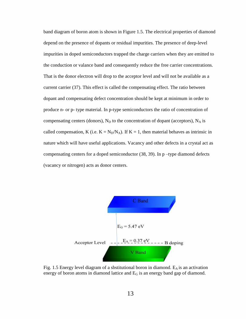
band diagram of boron atom is shown in Figure 1.5. The electrical properties of diamond
depend on the presence of dopants or residual impurities. The presence of deep-level
impurities in doped semiconductors trapped the charge carriers when they are emitted to
the conduction or valance band and consequently reduce the free carrier concentrations.
That is the donor electron will drop to the acceptor level and will not be available as a
current carrier (37). This effect is called the compensating effect. The ratio between
dopant and compensating defect concentration should be kept at minimum in order to
produce n- or p- type material. In p-type semiconductors the ratio of concentration of
compensating centers (donors), ND to the concentration of dopant (acceptors), NA is
called compensation, K (i.e. K = ND/NA). If K = 1, then material behaves as intrinsic in
nature which will have useful applications. Vacancy and other defects in a crystal act as
compensating centers for a doped semiconductor (38, 39). In p –type diamond defects
(vacancy or nitrogen) acts as donor centers.
Fig. 1.5 Energy level diagram of a sbstitutional boron in diamond. EA is an activation
energy of boron atoms in diamond lattice and EG is an energy band gap of diamond.

14
1.7 Conduction in Semiconductors:
Semiconductor is a material whose resistivity lies between that of a conductor and
an insulator. The conductivity of semiconductor can vary by several orders of magnitude
by introducing a suitable foreign element. Semiconductors can be an elemental material
like Si and Ge or a compound material like SiC, GaN, GaAs, AlN, and InP or an alloy
like Si1-xGex, Al1-xGaxAs, Hg1-xCdxTe. Diamond, however comprises of sp3 bonded group
IV element carbon and has a tetrahedral atomic structure like Si or Ge but it is not
considered as a semiconductor, because it does not have any free charge carrier to
conduct electricity. A semiconductor establishes its conduction properties through a
complex quantum mechanical behavior within a crystalline structure. The periodic nature
of crystalline lattice possesses energy bands in semiconductor and bands have a gap in
allowed energy states which are responsible for conduction. Bloch’s theorem explains the
detailed understanding of band structure (40). The Hamiltonian of the system with its
electronic eigenstates gives a basis for understanding electronic conduction in a material.
In a crystalline material the eigenstates, )(r are spatially extended Bloch states (41).
Due to the extended nature of the Bloch states, electrons with equal energy have an equal
probability2
)(r to be in every unit cell in space and are thus extended. The real crystal
is assumed to be weakly disordered due to defects and therefore conductivity is
dependent on the scattering of carriers from defects in the lattice. The perturbative
approach or percolation network theory is used to calculate conduction in such a crystal
(41). The band conduction and hopping conduction are the charge transport mechanism
in semiconductors. The schematics of carrier excitation in bands are shown in Figure 1.6.

15
Thermal holes and electrons are created in a semiconductor when electrons
undergo electronic transition from the valence band to the conduction band at sufficiently
high temperature. This is also called an intrinsic conduction of semiconductor. Wide band
gap semiconductors cannot have such conduction. The defects in semiconductor always
take compensating position i.e. defect has a p-type effect if semiconductor is an n-type
material and vice versa. Electron has a tendency to stay in lowest possible energy states
in a material. Hence electrons from a compensating donor level drop off to the acceptor
levels and produce ionized acceptors which are filled state of holes. At high enough
temperature some of the acceptors are also occupied by the excited electrons from
valance band and form acceptors holes in a valence band and ionized acceptors in
acceptor levels. The conduction due to the transition of electrons from a valence band to
an impurity band or vice-versa is called the band conduction in semiconductors. As the
temperature is reduced electrons from ionized (filled) acceptors begin to go back to the
acceptor holes in the valence band and give rise to band conduction. With the further
decrease of temperature all the electrons recombine their holes in a valence band and
produce saturation effect for conduction. At this point no change in conductivity is
recorded with some span of temperatures. If the temperature is reduced again further
there are only empty (unoccupied) acceptors in acceptors levels except for some ionized
acceptors due to compensating donors. Hence holes begin to hop from a filled impurity
band to an empty impurity band within the band gap. Such transition of carriers gives
hopping conduction. The details of hopping conduction are described below.

16
Fig. 1.6 Schematics of excitations of carriers in a compensated p-type semiconductor.
1.7.1 Hopping Conduction:
Hopping conduction is a phonon assisted quantum mechanical tunneling of charge
carriers. In a doped semiconductor charge carriers are located in localized states around
the impurities at low temperature. When charge carriers of a material jump (hop) in these
localized states of different energy, electric conduction occurs. Hopping nature of charge
carriers in localized states can be determined by the hopping probability (42-44).
Hopping probability ( hopP ) is the product of a tunneling factor )/2( R and a Boltzmann
factor )/( TkE Bij . R is a hopping distance and is the localization length (impurity
radius) that characterize the extension of wave functions in space. ijE is the energy
difference between sub states i and j. If the electronic wavefunctions of the two localized
states overlap, hopping takes place in the form of direct tunneling between the states. On

17
the other hand, when carriers trapped in localized states absorb a phonon to jump to the
next available site then thermally assisted hopping is taking place. Schematic of carriers
hopping from a filled site to an empty site by the absorption of a phonon is illustrated in
Figure 1.7. If 0 ijij EEE , The probability of a carrier to hop from a filled site to
any of the empty site (A, B or C) by the absorption of a phonon is given by the equation
]2
exp[Tk
ERP
B
ij
hop
(1),
and if 0 ijij EEE then the probability of hoping is given by equation
)2
exp(
RPhop (2)
In equation (2) TkB makes an important contribution to hop. For localized states, when
)/2()/( RTkE Bij then hopP is maximum for R minimum and conduction is nearest
neighbor hopping (NNH) (45, 46). The number of available states for hopping is small at
this case and Boltzmann factor will decrease the total hopping probability. The
conductivity at this point can be determined as follows:
The diffusion coefficient for hopping is
21RP
fD hophop (3)
Where f is the co-ordination number and for diamond 6f .
The conductivity is given by
TkEeENne Bf )()( (4)

18
Fig. 1.7 Schematics of carrier hopping mechanism in localized states (impurity band) of a
semiconductor. Here Ef, Ej and Ei are the energy of a Fermi level, an empty and a filled
state respectively.
Here, TkENn Bf )( , is the number of carriers per unit volume taking part in hopping
and have energy E such that TkEE Bf . The density of states )( fEN at the Fermi
level is given by
])(4[
33REN
Ef
ij
(5)
The mobility from the Einstein’s relation is given as
Tk
eD
B
hop
(6)
Hence the conductivity can be written as
]2
exp[)(6
1 22
Tk
ERRewEN
B
ij
of
Or, ]2
exp[)4
3(
6
1 2
Tk
ER
RE
ew
B
ij
ij
o
(7)

19
Hence the thermally activated hops can be characterized by
)/exp( 3 TkBo (8)
Equation (8) shows the temperature dependent behavior of hopping conductivity of a
system, ow is the factor depending on phonon frequency, N(E) is the density of state and
o is the pre exponential factor. The activation energy 3 ijE , is necessary for the
carrier to surmount coulomb potential between occupied and unoccupied sites.
If the temperature reduces further then spatial term begins to affect the conductivity
because ijE becomes small and R becomes large. This condition creates large number
of available states for carriers to be hopped i.e. Boltzmann factor enhances the large
hopping probability equation (1). This new regime is called Mott variable range hopping
(VRH). With the decreasing temperature, the hopping probability of both A and B
decreases but )(AP decreases much more then )(BP due to the large energy separation
( ijE ). Therefore, it is more favorable for a carrier to hop at a longer distance to find a
lower energy state (44, 45). In this case TkE Bij / is not negligibly small compared with
/2R , hence hopP is maximum for minimum )/()/2( TkER Bij . In order to
maximize hopP , at low temperature regime the localization centers R (hopping distance)
and energy separation ijE can be expressed by eqn. (5). )(REEij is the energy for
which the number of states in a radius R , with energy )(0 REE .
Now substituting )(RE for ijE in equation (1) we get
)2
exp(3R
aRPhop
(9)

20
Here, fB ENTk
a(4
3
, and the most probable hopping distance R is found by
minimizing the exponential term, i.e.
4
1
)(8
3
fB ETNkR
(10)
And, 4
14
3
)(3
8
4
3)(
f
Bij EN
TkREE
(11)
Substituting equation (11) into equation (7), the expression for conductivity is
4
1
exp
T
Too (12)
Here,
)(
3
fB
oENk
T
(13)
Which is a famous Mott’s 4
1
T VRH law.

21
CHAPTER 2
2.0 RESEARCH OBJECTIVES:
The objectives of this study were
1. To optimize the deposition parameters for the high growth rate and high quality
boron-doped single crystal diamond,
2. To investigate the influence of nitrogen on the growth process of the boron-doped
single crystal diamond, and
3. To understand the basic mechanism of temperature dependent resistivity in boron
doped single crystal diamond.
To achieve these goals, we have designed a new water cooled copper stage which
can be favorable to high growth rate and high quality of diamond. Substrate holder design
is one of the factors for better growth rate, as it directly relates to the substrate
temperature and plasma density. The concentration of microwave field changes according
to the holder shape. The higher the concentration of microwave field, the faster is the
deposition. High power and high pressure in CVD has been demonstrated recently for
high quality and low defect of single crystal diamond (47). In a single crystal diamond
deposition, the main challenges are the process control and the deposition growth rate.
Several designs of substrate holders and stages have been examined during the
experiment to optimize the process control. Some of them are discussed here.

22
80 mm(a) 80 mm
Copper Cap over
cooling drum
(b)
(c)
Fig. 2.1 Design of water cooling stages (a) stainless steel stage, (b) copper stage, and
(c) copper cap over cooling drum.
(a) (b)
Fig. 2.2 Design of substrate holders with shallow cavity (0.7mm deep and 4.5mm square
shape) (a) narrow holder (diameter 12mm, length 25mm), and (b) wide holder (diameter
22 mm, length 25mm).
23
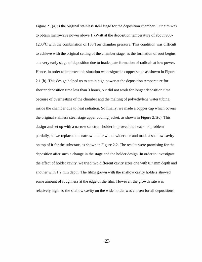
Figure 2.1(a) is the original stainless steel stage for the deposition chamber. Our aim was
to obtain microwave power above 1 kWatt at the deposition temperature of about 900-
1200oC with the combination of 100 Torr chamber pressure. This condition was difficult
to achieve with the original setting of the chamber stage, as the formation of soot begins
at a very early stage of deposition due to inadequate formation of radicals at low power.
Hence, in order to improve this situation we designed a copper stage as shown in Figure
2.1 (b). This design helped us to attain high power at the deposition temperature for
shorter deposition time less than 3 hours, but did not work for longer deposition time
because of overheating of the chamber and the melting of polyethylene water tubing
inside the chamber due to heat radiation. So finally, we made a copper cap which covers
the original stainless steel stage upper cooling jacket, as shown in Figure 2.1(c). This
design and set up with a narrow substrate holder improved the heat sink problem
partially, so we replaced the narrow holder with a wider one and made a shallow cavity
on top of it for the substrate, as shown in Figure 2.2. The results were promising for the
deposition after such a change in the stage and the holder design. In order to investigate
the effect of holder cavity, we tried two different cavity sizes one with 0.7 mm depth and
another with 1.2 mm depth. The films grown with the shallow cavity holders showed
some amount of roughness at the edge of the film. However, the growth rate was
relatively high, so the shallow cavity on the wide holder was chosen for all depositions.

24
CHAPTER 3
3.0 EXPERIMENTAL DETAILS:
A Type Ib (100) oriented HPHT diamond seed crystal of dimensions
3.5 × 3.5 × 1.5 mm3 was used as a substrate in a 6 kW, 2.45 GHz microwave reactor
system MPCVD (48, 49). Diborane diluted in 90% of hydrogen was used as a boron
source gas in this study (30, 50). In particular, 4 to 10% ratio of CH4 /H2, and 0.2% of O2
have been introduced in a total of 400 standard cubic centimeters (sccm) of feed gas. The
microwave power and pressure were varied from 1.35 – 2.0 kW and 95 - 140 Torr
respectively for the substrate temperature range of 900 to 1200oC. The p-type
conductivity of diamond films and their quality were tuned by introducing 0.5 to 3 sccm
of diborane in a feed gas.
3.1 Synthesis of Homoepitaxial Single Crystal Diamond:
To optimize deposition process, we first synthesized few undoped homoepitaxial
diamond films. Two of them are discussed here, the seed was ultrasonicated in acetone
before placing on a shallow cavity of molybdenum holder. The holder was mounted on a
cooling jacket. The first undoped diamond film was synthesized using 8% methane, 0.4
sccm of nitrogen, 0.8 sccm of oxygen and remaining hydrogen respectively. The
deposition temperature was set at 1100oC for 8 hours. The other one was deposited for 5
hours only with 6% CH4/H2 ratio and 0.8 sccm of O2 with the remaining hydrogen.
25
3.2 Synthesis of Boron-Doped Homoepitaxial Single Crystal Diamond:
Two sets of boron doped single crystal diamond films were synthesized
homoepitaxially with varying diborane from 0 to 750 ppm (B/Cgas from 0 to 25000 ppm)
content in a feed gas. Set-I was deposited to optimize temperature and other deposition
parameters like microwave power, chamber pressure and the deposition time. We have
deposited doped diamond films from the substrate temperature range of 900oC to 1200
oC
with the step of 100oC for 8 hours. After the optimization of the temperature, Set-II was
deposited for 5 hours at a fixed temperature of 1100oC. In Set-II, we have first optimized
the flow of diborane in the process gas and then investigate the effect of nitrogen on the
growth process of boron doping. Some of the samples in Set-II were grown in presence of
0.2% oxygen. The overview of experimental growth conditions for both the set of
depositions was summarized in Table 3.1 and 3.2.
3.3 Calculation of Boron to Carbon Ratio in Gas Phase (B/C)gas:
The dilution of diborane was 10000 ppm in hydrogen (10% in H2).Taking an
example of 6% methane in a feed gas, the B/C ratio in gas phase was calculated using
following procedure: the amount of boron atoms (twice the B2H6 concentration in ppm)
divided by the number parts of carbon (which will be 6/100 for 6% of CH4 flow). So
depending on the B2H6 flow (sccm) out of the total flow (sccm) in the reactor, the amount
of B2H6 (ppm) in the feed gas can be determined.
The B/C is equal to (2×B2H6 flow (ppm) / methane fraction.
i.e.
100/%2
4
62
CH
ppmHB
C
B
gas
(14)

26
So if there is 150 ppm B2H6, 6% CH4 in the feed gas, then B/C ratio will be (2×150/0.06)
ppm, which is 5000 ppm.
For conversion of standard cubic centimeters per minute (sccm) to parts per
million (ppm), suppose total flow of gas is 400 sccm which we distribute into 106 parts,
so if we use 0.6 sccm of diborane (B2H6) which is diluted in hydgrogen by 10% then only
0.06% of B2H6 is only going into the feed gas hence from unitary method
we have 400 sccm = 106 (1 million parts)
1 sccm = 106/400 ppm (parts per million)
Therefore, 0.06 sccm of B2H6 = (106/400)×0.06 ppm = 150 ppm.
3.4 Cleaning of Films after Deposition:
The films of Set-I were cleaned in saturated solution of CrO3 + H2SO4 solution at
150oC for 5 minutes, 10 minutes of rinsed in a 1:1 boiling solution of H2O2 and 30%
NH4OH with the final rinse in deionized water and 10 minutes of ultrasonication in
acetone (51). Finally, the samples were exposed in hydrogen plasma at 900oC for 10
minutes before further characterization. To avoid any ambiguity due to hydrogenation
electrical resistance measurement was taken during cool down procedure in a four point
probe vacuum chamber. The Set-II samples were characterized without further cleaning
after deposition. However, mechanical cleaning of boron soot at the edges of samples has
been scratched with the sharp knife and final rinsed with acetone ultrasonication. In order
to ensure ohmic contact conditions with bulk limited currents, the currents through the
samples were limited to 0.1 to 1.0 mA.

27
Table 3.1. Overview of experimental growth conditions (Set-I), growth rate (r) and boron
concentrations (calculated from four point probe measurement data above transition
temperature) in the grown diamond films. Total feed gas flow rate was 424 sccm.
Sample Temp.
(oC)
Power
(kW)
Pressure
(Torr)
r
(μm/h)
[B/C]gas
(ppm)
B2H6
(ppm)
[B]
(atom cm
-3)
HD1
BD1
BD2
BD3
BD4
1050
1100
1000
1200
1100
1.5
1.5
1.2
2.5
1.6
75
95
80
140
110
23
16
10
8
2
0
2300
4700
6200
6200
0
90
140
190
190
0
2.4×10¹⁸
-
2.2×10¹⁹
1.0×10²⁰
*HD1 was grown in 8% of CH4 and additional 0.4 sccm of N2.
BD1 was grown in 8% of CH4 and BD4 was grown only in 318 sccm of total gas flow rate.
Table 3.2. Overview of experimental growth conditions (Set-II), growth rate (r) and
boron concentrations (calculated from four point probe measurement data above
transition temperature) in the grown diamond films. Total feed gas flow rate was 400
sccm.
Sample r
(μm/h)
B2H6
(ppm) [B/C]gas
(ppm)
%
CH4
N2 [B]
(atom cm
-3)
HD2
BD5
BD6
BD7
BD8
BD9
BD10
BD11
BD12
BD13
10
6
5
4
6
3
7
2
8
12
0
150
250
500
500
750
150
150
150
500
0
5000
8000
16000
16000
25000
5000
7500
4000
16000
6
6
6
6
6
6
6
4
8
6
0
0
0
0
1000
0
0
0
0
2000
5.5×10¹⁷
1.1×10¹⁹
6.6×10¹⁹
2.3×10²⁰
3.9×10¹⁹
-
-
-
-
-
*all samples are grown in additional 0.8 sccm of O2, BD10 was grown for 15 hrs.

28
3.5 Characterizations:
In order to understand the vapor phase growth mechanism, surface morphology
and doping behavior of single crystal diamond by various characterization techniques
have been utilized in this study. An optical transmission spectroscopy was used to
quantify effect of boron on the appearance of diamond color. An optical emission
spectroscopy (OES) was used to analyze in situ excited species during the growth
process. The surface morphology of samples was characterized by optical microscope
(OM), and atomic force microscope (AFM). The crystal phase and purity was verified by
X ray rocking curve experiment and Raman spectroscopy. Doping level was determined
by FTIR spectroscopy and finally electrical conductivity and number of charge carriers
were calculated using four point probe and Hall measurement.
3.5.1 Optical Transmission Spectroscopy:
The effect of doping on color of the film has been analyzed using Horiba
Microscope paired with Transmission Spectrometer in the visible range.
3.5.2 Optical Emission Spectroscopy (OES):
A hot gas or plasma emits electromagnetic radiation of different wavelengths at
low pressure which is characteristics of atoms, ions and molecules within the plasma. The
spectral analysis is the sorting of this radiation as a function of wavelength and is called
an emission spectrum. Optical emission spectrum is well known in-situ and non-invasive
technique for plasma diagnostics. It can provide information about properties of materials
within the plasma such as excited species densities, energy distribution of species, and

29
temperature of plasma (52, 53). In OES, light emitted by electronically excited species is
collected and detected. The transition from electronic ground state and excited states
contain both vibrational and rotational states. An emission from a particular electronically
excited state therefore consists of a number of emission lines corresponding to transition
from the rotational/vibrational sublevels. Hence such electronic spectrum is used to
identify emitting species (54-57). The analysis done here was to find the types of species
present in the plasma rather than deducing the absolute concentration of species. The
observed species in the H2/CH4/N2 and H2/CH4/B2H6 plasma are listed in Table 3.3.
Acton Research Corporation SpectraPro 500i, 0.500 meter triple grating monochromator /
spectrograph, has been used in this study with a 1200 grating/mm blazed at 300 nm. The
details of the result are discussed in Section 4.2.
Table 3.3 Observed species in OES of H2/CH4/B2H6/N2/O2 plasma.
Species Peak Position (nm)
Hα
Hβ
Hγ
658.6
488.2
433.2
H2 602.1
CH 431.4,
388.9
CN 360.58, 388.6, 421.6
C2 472.6, 516.5, 563.5,
BH 432.8

30
3.5.3 Optical Microscopy (OM):
High resolution optical microscopy has been widely used technique to
characterize the surface morphology of the diamond deposition. It gives information on
the presence of non-epitaxial deposition, growth sectors, and growth twins and other
imperfections on the surface or at the corner of the diamond. Crystal imperfection is often
observed in high microwave plasma density (MWPD) deposition. The Wild/Leica M420
optical microscope and Fisher scientific micromaster optical microscope were used in
this study for micro-photography of the samples.
3.5.4 Atomic Force Microscopy (AFM):
It is a high resolution scanning probe microscope. It relies on mechanical force of
atoms between the tip (probe) and the sample. It is a widely used tool for the surface
topographic image of sample at nano – scale. It is composed of a cantilever with a tip at
the end that scans on the surface. AFM can be divided into two basic scanning modes,
contact mode, and non-contact mode. In contact mode when probe is brought in to the
proximity of the varying topographic features forces between the tip and samples lead to
the deflection of the cantilever according to Hook’s law (58). This deflection can then be
measured by the using reflected laser spot from cantilever into a photodetector. In contact
mode tip can acquire electrostatic charge by friction from the surface and reduces the
actual force to detect and can also damage the sample or can dull the tip. In non-contact
mode cantilever is oscillating at its resonant frequency near the sample surface which
causes to change in force between tip and sample. These changes in forces are referred to
as force gradient. The force gradient changes the amplitude and phase of oscillation of

31
the cantilever which can be measured by the detector. Thermomicroscope’s TM Explorer
AFM instrument with Veeco probe in contact and non-contact mode was used to measure
surface morphology in this study.
3.5.5 Raman Spectroscopy:
Raman spectroscopy is a non-destructive technique to characterize various carbon
phases present in CVD diamond. It is based on inelastic scattering of monochromatic
laser radiation. When sample is illuminated with monochromatic laser light, some of the
re-emitted photons from the sample change (shift) its original frequency. This change in
frequency provides information about the vibrational, rotational or other low frequency
transitions in a system. Atomic or molecular vibrational energy is used to identify sample
quality in Raman spectroscopy. Both Raman and IR spectroscopy are based on
vibrational modes in the system. We have employed both techniques in our
characterization of homoepitaxial diamond. Asymmetric stretch in system is IR active
(59). The 532 nm line of solid state laser is used in this study as an excitation source and
the detection of the Raman signal was done in 180o configuration by a Dilor XY
spectrometer combined to a Pulnix CCD camera.
3.5.6 Single Crystal X-ray Diffraction (XRD) and Rocking Curve Experiment:
The single crystal x-ray diffraction technique was utilized to study the crystalline
quality of homoepitaxial boron-doped diamond films (60). The crystal perfection was
investigated by performing the rocking curve measurement on the (400) Bragg reflection
from the CVD diamond. In rocking curve experiment scan is performed by rotating

32
sample with an angular step (Δω of 0.02 degree) and a detector is fixed at (2) Bragg
position with the incident beam. A precise value of Bragg angle for (400) position was
first obtained using powder diffraction 2 scan for rocking curve experiment. Once this
value is determined the detector is fixed at (2) Bragg position with the incident beam
and then omega scan is performed by rotating sample with 0.02o angular step. Defects in
crystal broaden the intrinsic rocking curve (61). Philips X- ray diffractometer, model
(PW3040) with monochromatic CuK radiation has been used in this study for powder
diffraction pattern and Omega scan of the samples. A nickel filter was used to eliminate
the CuK. Philips X’Pert organizer software was used for data acquisition.
3.5.7 Fourier Transform Infrared Spectroscopy:
All the atoms in a molecule or substance are vibrating in a characteristic
frequency with respect to each other above absolute temperature. If the frequency of a
specific vibration of atom is equal to the frequency of IR radiation passing through the
sample, then IR radiation gets absorbed by the substance. Measurement of such IR
frequencies absorption by a sample is studied in Infra-red spectroscopy. To analyze the
signal of different frequencies with their intensity a mathematical operation Fourier
transformation is performed via computer, hence the term FTIR. Vertex 70 FTIR
spectrometer with Bruker optics hyperion 3000 IR microscope was used in this study for
FTIR spectra of the films.
33
3.5.8 Diamond Surface and Metallic Contact:
In order to study electrical properties of semiconducting CVD diamond films,
metallic contact is necessary. Two types of metallic contact are made on semiconductor
surface: Ohmic (non-rectification) and Schottky (rectification) contacts. When metal is
brought in contact with the semiconductor a potential barrier is formed between the
surfaces due to transfer of charges to equalize the Fermi levels. This barrier is called
Schottky barrier which has a non-linear response to I-V characteristics. Hence it is very
difficult to obtain good Ohmic contact between metal-semiconductor (MS) interfaces.
However, one can minimize the barrier height by selecting the metal work function
nearly similar to semiconductor on which metallic contact has to be made. The Table 3.4
and Figure 3.1 are given below to explain the formation of barrier between metal-
semiconductor interfaces. Charges are trapped in the depletion region between metal-
semiconductor interfaces by forming Schottky junction as shown in Figure 3.1 (d) but
Ohmic contact is formed with no charge traps between the interfaces as shown in Figure
3.1 (c). Space charge limited region is formed on the interface if work function of metal
( m ) is less than that of p-type semiconductor ( s ) (62). Boron doped diamond has a
work function about 5.16 eV and Tungsten (W) has about 4.65 to 5.70eV depending upon
its crystal orientation (63) and also tungsten shows good adhesion on diamond surface
(64). We deposited tungsten on the surface of Set-I diamond by magnetron sputtering for
electrical characterization. Electrical characterization of Set-II samples was performed
using silver epoxy on the surface of diamond film.

34
Table 3.4 Electrical nature of ideal MS contacts.
Work function n-type semiconductor p-type semiconductor
sm Rectifying Ohmic
sm Ohmic Rectifying
(a)
(b)
(c)
(d)
Fig. 3.1 Energy band in metal-semiconductor systems before contact (a) sm , and (b)
sm ; metal-semiconductor junction after contact (c) sm , and (d) sm .

35
3.5.9 Four Point Probe and Hall Measurements:
The electrical properties of the samples were determined by four point probe and
Hall measurement techniques. Measurements were taken in linear configuration in four
point probe. The resistivity of the sample was determined by the following formula
)/(.2
stFtLn
R
, (15)
Where ,, R and t are resistivity, resistance, and thickness of the film and s is spacing
between two probes (65). Since st , the correction factor )/( stF is assumed to be equal
to unity. MMR technology four probes system with the help of Keithly 237 instrument
was used in this study.
Hall measurements were performed at room temperature in van der Pauw
configuration with Ecopia HMS-3000 instrument. The I-V characteristics were
maintained during experiment by limiting the current supply within 1mA at zero –
magnetic field. The value of sheet resistance was measured in magnetic field of 0.55
Tesla. The measurements were taken for both positive and negative current with both
polarities of magnetic field. P-type of doping was determined by Hall measurements.

36
CHAPTER 4
4.0 RESULTS AND DISCUSSION:
4.1 Optical Transmission Spectra:
A series of homoepitaxial boron doped single crystal diamond films were
synthesized with different level of boron doping and characterized in this study. The
color of seed crystal was observed to change from yellow to pale blue then to dark blue
and finaly opaque as boron concentration was increased in the films. Optical transmission
spectra of the samples in the visible range were taken in order to measure the effect of
doping on the color of the films. The spectra indicate small downshift of peak and
decrease in transmitted intensity as the doping level of the films increases. The peak of
low doped film (sample BD5) appeared at 454 nm in the optical transmission spectra, as
shown in Figure. 4.1.

37
Fig. 4.1 Optical transmission spectra of seed crystal (Seed) and doped diamond films
after applying correction for the absorption in the diamond seed crystal. Photographs of
seed crystal (Seed) and doped diamond (BD6) are embedded inside the graph. Yellow
color in seed is due to substitutional nitrogen atom in diamond lattice and bluish color in
BD6 represents boron incorporation in the diamond lattice.
4.2 Optical Emission Spectra:
To detect excited species within the plasma during the diamond growth process,
an optical emission spectroscopy was used. The spectral peak(s) observed during the
diamond growth process with and without diborane are labeled corresponding to the
excited species and is shown in Figures 4.2. Visible range of emissive scan showed very
intense Balmer series of atomic hydrogen and diatomic hydrogen and carbon, CH and CN
molecules. The atomic hydrogen lines produce singlets while diatomic species such as
C2, H2, and CH produce doublets. Several C2 bands from Swan band system were also

38
detected throughout the visible range. The strongest C2 band is in the green region at
516.5 nm. The observed species in OES of H2/CH4/B2H6/N2 /O2 plasma have been
summarized in Table 3.3. Addition of oxygen in source gas did not significantly change
the emission spectrum. Change in spectrum has been observed when nitrogen gas was
removed and the diborane gas was introduced for the deposition as shown in Figure 4.2.
High power and pressure may reduce the intensities of the peaks and absence of nitrogen
removed the nitrogen related peaks. Literature shows that atomic boron OES peaks
appear at around 250 nm and BH radicals appear at 432.8 nm (52). We were unable to
observe peak at 250 nm but peak at 432.8 nm seemed to be overlapping with other peaks
as shown in Figure 4.2. Because the high percentage of hydrogen gas was used as the
source gas a high concentration of atomic (H and molecular (H2) hydrogen was visible
in the spectrum. High amount of atomic hydrogen is needed to produce active carbon
radicals during diamond deposition.
The increase in flow rate of nitrogen was observed to increase the intensity of CN
band but did not show noticeable effect on the other species such as C2 dimer as shown in
Figure. 4.3. The increase in growth rate suggests that the nitrogen causes surface catalytic
reaction. The addition of nitrogen increases the surface kink density that provides the
sites to incorporate active carbon species. Atomic hydrogen increases the growth rate by
increasing the number of active surface sites or shifting the balance among adsorption,
desorption and incorporation steps (66). Locher et al and Wolden et al suggests that
atomic hydrogen affects the growth rate by enhancing the sp3
componet. In contrast,
nitrogen additon affects the growth by inhibiting the sp2 component. However, excess
nitrogen creates negative effects on the sp3
component (67, 68).

39
Fig. 4.2 Optical emission spectra of H2/CH4/N2 plasma under the pressure, power and
temperature of 80 Torr, 1.5 kw and 1100oC respectively (red color) and H2/CH4/B2H6
plasma under the pressure, power and temperature of 100 Torr, 1.5 kW and 1100oC
respectively (green color).
10000
8000
6000
4000
2000
0
Inte
nsi
ty (
a.u
.)
700650600550500450400350300
Wavelength (nm)
N2 = 1.2 sccm
N2 = 0.8 sccm
N2 = 0.4 sccm
N2 = 0 sccm
CN
CN
C2
C2
C2
H
H
BH/H
H2
CH
H2
Pressure ~ 100 TorrPower ~ 1.4 kWatt B2H6 = 16000 ppm
Fig. 4.3 Optical Emission Spectroscopy (OES) results from the plasma during the
diamond deposition process. The spectra shown were obtained for various levels of
nitrogen in the plasma at a fixed concentration of diborane.

40
4.3 Optical Microscopy Images:
The surface morphology of diamond films had been observed using optical
microscope. The untreated HPHT substrate (seed crystal) has shown macroscopically flat
surface with <100> crystal plane. The image of homoepitaxially deposited diamond film
(HD1) shows round hillocks and twins on the film surface. This film was deposited in 8%
of CH4-H2 gas, 900 ppm of N2 and 1800 ppm of O2 with a total 434 sccm of feed gas. The
deposition temperature, microwave power, and chamber pressure was maintained at
1050oC, 1.5 kW, and 75 Torr respectively. The edge of the film was observed to be very
rough. The roughness at the edge of film may be due to the formation of bright ring of
plasma at the edge of the substrate. Formation of twins and hillocks may be assumed to
be the effect of instability in plasma due to process control. The problem in process
control in MPCVD is normal because the leakage of e-m wave inside the chamber is
obvious, lack of uniform cooling system of substrate during the long deposition time and
the high thermal conductivity of hydrogen gas which can heat the chamber wall in long
run of deposition time. If the substrate is mounted in a holder above the cavity then a very
bright rim of plasma is formed around the edge of the sample may cause the edge
roughening. This explanation was verified with nearly smooth edge of sample deposited
by placing the substrate in the cavity as flushed where substrate edges are not exposed to
plasma. Optical microscope images of some of the samples are shown in Figure 4.4 and
4.5. The flow of diborane in source gas causes the formation of carbon-boron soot and
darkening of chamber wall in long deposition time. In the absence of plasma activation,
enhanced soot formation is noted (49). The growth condition of Set-I and Set-II is given

41
in Table 3.2. The experiment was performed at microwave power density (MWPD) of 90
to 100 W/cm3.
In Set-II, the experiment deposition temperature was fixed at 1100oC with 1.4 -
1.5 kWatt microwave power and 100 Torr chamber pressure. The deposited
homoepitaxial film HD2 shows some non-epitaxial deposition on its surface but no twins.
The ratio of methane and hydrogen was 6% with a total feed gas flow rate of 400 sccm.
The deposition conditions have been shown in Table 3.2. The films either grown at high
percentage of diborane or longer deposition time show polycrystalline in nature as shown
of sample BD9 (3 sccm of diborane) and BD10 (0.6 sccm of diborane for 15 hours
deposition) respectively in Figure 4.5. More hillocks were seen on the surface of the
samples grown at both low and high methane content as shown in samples BD11 and
BD12. The optical microscope images below are showing the gradual improvement in
quality. The deposition temperature, flow of gases, cleaning of substrate with H2/O2
plasma before deposition and other deposition parameters have been selected after
performing a series of experiment in Set-I. All the substrates have been exposed to 4% of
O2/H2 plasma for 10 minutes before deposition begins. The growth rate and surface
morphology was found to be dependent on B/C ratio in the gas phase. High B/C ratio
with low methane in feed gas decreases the growth rate as summarized in Figure 4.6. The
optimal growth with good quality had been observed with 2 sccm (16000 ppm) of
diborane in feed gas. The quality was improved with the additional supply of 1000 ppm
of nitrogen in feed gas as shown of sample BD7 (16000 ppm of B2H6) and BD8
(additional 1000 ppm of N2) in Figure 4.5. However, the quality degraded by forming
hillocks with the addition of further increase of nitrogen to 2000 ppm, but it improved the

42
growth rate of diamond films by a factor of two as compared to 1000 ppm of nitrogen as
shown of samples BD8 and BD13 in Figure 4.6. Addition of a little amount of nitrogen
and low (B/C)gas ratio in feed gas may be the cause of high growth rate of sample BD1.
On the other hand, the same (B/C)gas ratio in samples BD3 and BD4 but less supply of
hydrogen and methane in feed gas for sample BD4 may have caused the reduction in
growth rate of sample BD4. It can be concluded from the above discussion that a proper
amount of diborane and nitrogen is favorable for improving the structural quality and
growth of boron-doped single crystal diamond.

43
Fig. 4.4 Optical microscopy images of substrate (Seed Crystal), undoped sample (HD1)
and boron doped diamond samples (BD1, BD2, BD3, and BD4) showing surface
morphological change on epitaxial deposition.
Fig. 4.5 Optical microscopy images of homoepitaxially deposited diamond samples
showing change in surface morphology with boron concentration in feed gas. Film BD8
and BD13 was deposited with additional introduction of nitrogen in feed gas (table 3.2).

44
Fig. 4.6 Histogram of growth rate of boron doped diamond as a function of B/C ratio in
gas phase. All the depositions took place at 1100oC, 1.4 kW microwave power and about
100 Torr chamber pressure. The amount of diborane used for BD7, BD8 and BD13
growth was same. The amount of CH4 gas was described in table 3.2.
4.4 Atomic Force Microscopy Images:
AFM images were taken of the flat surfaces of the epitaxial films over scanned areas of
20 × 20 µm2 (Set-I) as shown in Figure 4.7. The surface morphology of the undoped and doped
films was seen modified after deposition. The polishing scratches of the seed crystals
disappeared and step flow morphological features were observed after deposition. Groove shaped
features seen on the surface of sample BD4 may be the result of step bunching as shown in Figure
4.7. Step asymmetry during deposition may be the cause of step bunching in CVD (69-72).
In order to compare growth rate and surface morphology of doped and undoped diamond film the
sample (HD1) was grown without using diborane in the feed gas. Presence of diborane in feed
gas prevent formation of microtwins and hillocks on diamond film, as shown in Figure 4.4 and

45
Fig. 4.7 AFM images of seed crystal (seed), the magnified view at top right corner shows
the polishing scratches and the carbon debris on the substrate before any CVD treatment,
undoped sample HD1 and boron doped single crystal diamond samples (BD1, BD2, BD3,
and BD4). The deposition time for this study was 8 hours.

46
4.6. In sample (seed) polishing lines (which are trace of mechanical polishing in HPHT
production) are seen periodic and parallel to each other. The formation of steps, kinks and
terraces (sample HD1 in Figure 4.7) are normal phenomena in step flow growth
mechanism of diamond. Additional information in step flow growth and step bunching
can be found in (71-75).
In order to study the effect of boron and nitrogen on the growth morphology of
diamond, few samples were grown at varying diborane and nitrogen contents in feed gas
for 5 hours deposition. The growth conditions are summarized in Table 3.2. The contact
mode AFM images over scanned areas of 10 × 10 µm2 for Set-II are shown in Figure 4.8.
The rms roughness of the samples was observed to decrease with increasing boron
concentration in feed gasses (samples BD5, BD6 and BD7). Introduction of 1000 ppm of
nitrogen during boron doping improved the surface morphology and increased the growth rate of
film (sample BD8). However, when higher amount of nitrogen 2000 ppm along with the same
16000 ppm of B/C ratio was used, the growth rate of film was shown to double than that using
1000 ppm of nitrogen. On the other side, higher amount of nitrogen reduces the film quality as
some non-epitaxial features are seen on the surface of the film as shown in sample BD13 of
Figure 4. 5.
Samples BD11 and BD12 were grown with 4 and 8% of methane by keeping a
constant diborane flow at 150 ppm. As we see here low methane gives smooth surface
but reduces the growth rate and on the other hand high methane produced very rough
surface but high growth rate in the grown experimental condition. From OM image of
sample BD12 in Figure 4.5 we can see that it has high hillocks density and non-epitaxial
crystallite on its surface. When high diborane 750 ppm or high methane 10% was

47
Fig. 4.8 AFM images of homoepitaxial sample (HD2), boron doped single crystal
diamond samples (BD5, BD6, BD7, BD8 and BD13). AFM images of boron doped
diamond samples (BD11) and (BD12) grown at 16 sccm and 32 sccm of methane. AFM
images of BD9 and BD10 are not shown here. The deposition time was 5 hours.

48
introduced in the deposition chamber amorphous carbon and polycrystalline nature of
diamond film was grown on seed crystal as shown in OM images of samples BD9 and
BD10 in Figure 4.5. Overall, there is a significant decrease in diamond growth rate with
an increase in boron content in the plasma as summarized in Tables 3.1 and 3.2.
4.5 X-ray Diffraction Pattern and Rocking Curve:
The quality of the film was also tracked with an x-ray powder scan and rocking
curve experiment as shown in Figure 4.9. The intense peak of (400) Bragg reflection was
observed at 119.8o in powder scan and a single intense peak of (400) was observed in the
rocking curve experiment from 30-62o omega scans indicating high quality film inset of
Figure 4.9. The FWHM of the Bragg peak was observed to be broadened and varied from
0.07o to 0.10
o with increasing boron content in the films. Few week peaks due to trace
elements from seed crystal are also observed in the powder scan. Transition metals or
their alloy have been used in the HPHT synthesis process to grow seed crystal. Those
trace metals may invite the non-epitaxial growth in CVD diamond deposition and have
detrimental effect for single crystal diamond.

49
Fig. 4.9 XRD pattern of a as received seed crystal (seed), undoped film (HD) and boron
doped diamond film (BD). The inset is the rocking curve for boron doped diamond film.
4.6 Raman Spectra:
The Raman spectra of doped and undoped single crystal diamonds are shown in Figure
4.10 (a, b and c). No graphitic carbon related peak was observed in the spectrum indicating high
quality of homoepitaxial layer. Doping was found to be uniform in its thickness as we
investigated the spectrum inside the film for few microns depths, as shown in Figure 4.10 (c). An
intense zone-center optical phonon mode of diamond is visible at 1334 cm-1
along with additional
broad bands at 580, 900, 1042, 1233 cm-1
. At low doping, no asymmetry in Raman line and no
additional band were observed in the spectrum. The observed additional bands at lower
wavenumber were previously reported mainly on polycrystalline boron-doped diamond (3, 76,
77). The significant modification in zone center optical phonon line was observed. The

50
asymmetry in optical phonon Raman line was seen increased with doping level. A small
downshift of bands 1233 and 580 cm
-1 with increasing boron concentration was also observed in
this study (77). The downshift of optical phonon line and broadening of full width at half
maximum (FWHM) with a significant change in intensity of bands 580 and 1233 cm-1
were also
observed. The origin of those additional bands is not completely understood yet but the literature
shows that bands around 1233 and 580 cm-1
are attributed to the presence of large cluster of boron
atoms in diamond (30, 76, 79). The downshift of optical phonon line with increasing boron
content has also been described by Gheeraert et al (80). The asymmetric broadening and
downshift of Raman peak of boron-doped diamond films could be explained by Fano-effect (81-
85). Fano effect is the quantum mechanical interference between discrete zone-center optical
phonon state and continuum of electronic states induced in presence of boron. The Raman peak
position and FWHM was calculated by Lorentzian fit of the spectrum. The Fano asymmetry of
diamond was derived by excellent fits of the Raman curves, as shown in inset of Figure 4.10 (c).
The Fano asymmetry of doped diamond BD7 was calculated to be (q = 9.2) and for seed crystal
q = 492. The Fano profile used in this fitting was,
Cq
II o
)1(
)(2
2
(16)
here C is constant, oI is prefactor and
o ; where and o are Raman peak position
of doped diamond and seed crystal respectively and is FWHM of a Raman curve of sample
BD7 (84).

51
Fig. 4.10 (a) Raman spectra of Set-I of samples undoped film HD1, boron doped films
BD1, BD2 and BD3 and as received seed crystal (Seed).
Fig. 4.10 (b) Raman spectra of Set-II of samples as received seed crystal (Seed), undoped
film HD2 and boron doped films BD5, BD6, BD7, BD8 and BD9. Insert (a) and (b) are
showing the peak shift and FWHM of samples in unit of cm-1
.

52
(c)
Fig. 4.10 (c) Raman spectra at different depth in sample BD7. Insets are Fano line shape
fitting with Raman curve of samples BD7 and Seed crystal to measure deformation in
optical phonon line due to doping.
4.7 Fourier Transform Infrared Spectra:
The boron concentration of Set-I samples were determined from absorption
spectrum of FTIR spectra. Strong absorption was seen in IR Spectra of the films above
2000 cm-1
wavenumber as shown in Figure 4.11. The one–phonon absorption peak at
about 1290 cm-1
was used to calculate boron concentration (82)
)1290(
1731)101.2()(][
cmcmB (17)
where tA/ , is the linear absorption coefficient at 1290 cm-1
band, and A and t
being absorbance and thickness of the film. In order to calculate concentration FTIR
spectrum first converted into absorption spectrum after that seed (reference) spectrum

53
was subtracted from it. The boron concentration in film of samples BD1, BD2 and BD3
was found to be 8.6×10¹⁸
, 1.5×10¹⁹
and 3.6×10¹⁹
cm-3
respectively. Due to strong
absorption to infrared signal, the FTIR spectrum of sample BD4 was not obtained hence
its dopant level could not be estimated using equation (17).
Characteristics Boron Peak
Fig. 4.11 FTIR spectra of as received seed crystal (seed), undoped diamond film HD1
and I set of boron doped diamond films BD1, BD2, BD3. Inset is the spectra after
applying correction for the transmission of seed crystal, characteristics boron peak is
shown at 1290 cm-1
.

54
4.8 Electrical Conductivity Measurements:
Conductivity of the grown diamond films have been measured as a function of
temperature using four point probe measurement system. The four point probe measurement
was conducted in vacuum with a pressure less than 5 mTorr. Nitrogen gas was used to cool the
samples in a four point probe system. To measure electrical conductivity, tungsten strips were
deposited on the surfaces of the diamond films using a magnetron sputtering technique. An
optical microscope image of the tungsten strips on a film surface is shown in Figure 4.12. The
currents through the samples were limited to 0.1 to 1.0 mA in order to minimize self-heating of
the samples and ensure ohmic contact conditions with the bulk limited currents. The variation in
conductivity, (σ) of the films with temperature (T) was determined from four point probe
measurement as shown in Figure 4.13. The room temperature resistivity of the most heavily
doped sample BD4 was determined to be 0.12 Ωcm. Activation energies of the samples have been
obtained by best fit Arrhenius plot of the conductivity data at high and low room temperatures
from the transition point. The activation energies of samples are listed in Table 4.1. The
difference in activation energy from high to low temperature indicates that the two different
conduction mechanisms are responsible for carrier transport in the film (81, 82). At higher
temperatures, carrier is transported via band conduction and at low temperatures, carrier hops in
the localized states via hopping conduction. At high temperatures, the activation energy of
carriers was found to decrease with increasing doping concentration. Increasing doping
concentration increases the acceptor band width which ultimately reduces the activation energy of
acceptors (85). A transition in the conduction mechanism from localized hopping to band
conduction was observed to shift towards higher temperature as the amount of doping increased.
However, in Set-II of samples this transition is seen to shift towards lower temperature with
increasing boron content in the film. The reason for such shift is not much clear yet, but the one
possibility could be the change in carrier mobility in the diamond film with increasing boron

55
concentration. Scattering centers for carriers, residual impurities, non-epitaxial growth and grains
all have diverse effect on carrier mobility. The variable range hopping conductivity of Set-I and
Set-II is shown in Figure 4.14 (a and b). The conductivity of films at lower temperature region
obeys Mott T-0.25
law.
The Pearson and Bardeen formula was also taken into account to estimate the boron
concentration, aN of the films from the calculated activation energy, aE (86).
3/1)( aoa NEE (18)
here eVEo 37.0 , is the activation energy of an isolated dopant, and is a material dependent
constant whose value for diamond is 6.7 × 10⁻⁸
eV/cm. The boron concentrations in samples BD1,
BD3 and BD4 were estimated using equation (18) to be 2.4×10¹⁸
, 2.2×10¹⁹
, and 1.0×10²⁰
cm-3
respectively. These values lie close to the estimated values of the dopant level determined from
the FTIR data at high temperatures. The boron concentrations in samples BD6, BD7 and BD8
calculated from room temperature Hall measurement were 6.6×10¹⁹
, 2.3×10²⁰
, and 3.9×10¹⁹
atom
cm-3
respectively and that calculated from a four point measurement above transition temperature
were 3.6×10¹⁹
, 0.6×10²⁰
and 2.7×10¹⁹
respectively.

56
Table 4.1 Activation energies of doped films measured in four point probe experiment.
Samples Above Transition Temperature. Below Transition Temperature
BD1
BD2
BD3
BD6
BD7
BD8
0.27 eV
0.18 eV
0.05 eV
0.19 eV
0.10 eV
0.16 eV
0.02 eV
0.05 eV
0.03 eV
0.02 eV
0.02 eV
0.01 eV
BD
Fig. 4.12 Tungsten strips on doped diamond for metallic contact.
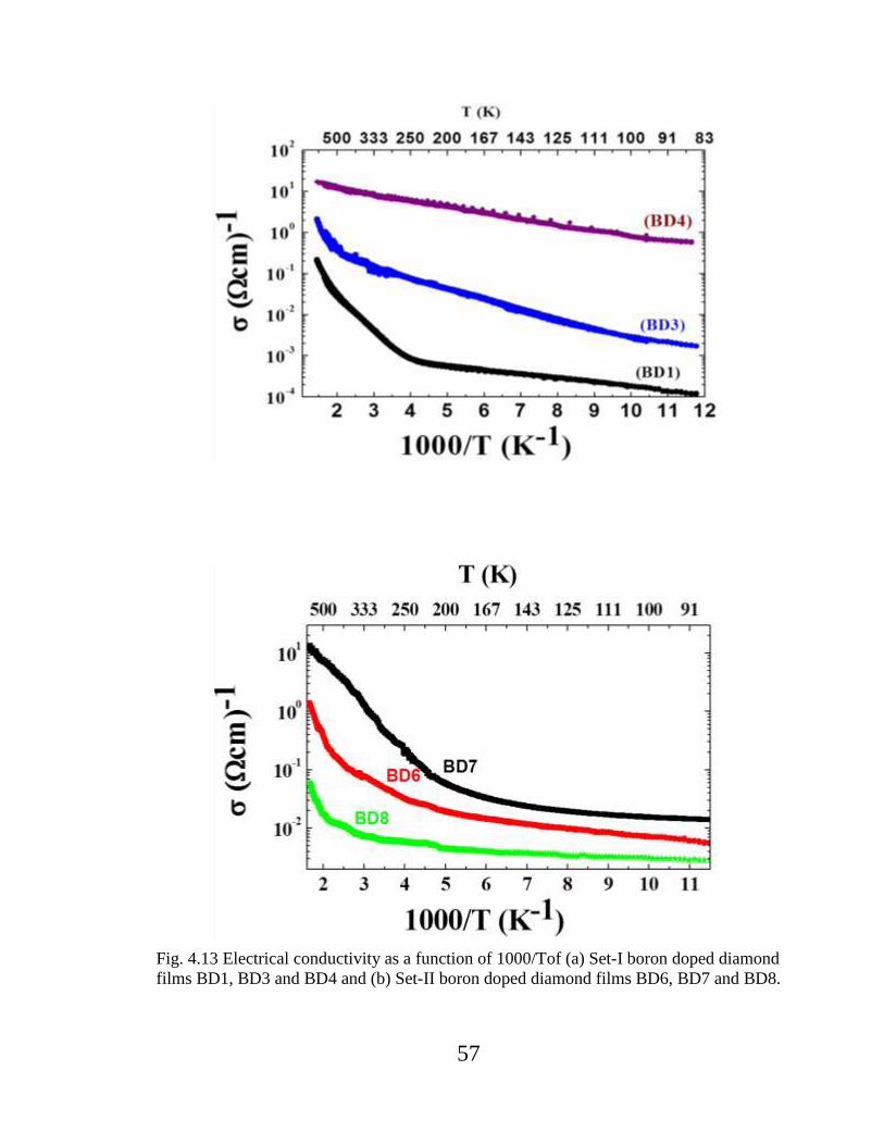
57
Fig. 4.13 Electrical conductivity as a function of 1000/Tof (a) Set-I boron doped diamond
films BD1, BD3 and BD4 and (b) Set-II boron doped diamond films BD6, BD7 and BD8.

58
Fig. 4.14 Electrical conductivity as a function of T-0.25
of (a) Set-I boron doped diamond
films BD1, BD3 and BD4 and (b) Set-II boron doped diamond films BD6, BD7 and BD8.

59
CHAPTER 5
5.0 CONCLUSIONS:
Boron-doped single crystal diamond has been synthesized using microwave
plasma chemical vapor deposition on commercially available synthetic Type-Ib diamond
substrates. The homoepitaxial diamond films were grown with boron-doping levels of
1018
to 1020
cm-3
. The color of seed crystal was seen to change from yellow to pale blue,
then to dark blue, and finally to completely opaque as the doping concentration in the
film increased. The effect of nitrogen in the growth plasma on boron doping was also
investigated during this study. Nitrogen shows both positive and negative effects on
boron doped diamond film. Surface morphology and growth rate of diamond deposition
improved with the use of 1000 ppm of nitrogen, but when the amount of nitrogen was
increased to 2000 ppm, non-epitaxial growth appeared on the surface of the doped film.
On the other hand, either the boron incorporation in diamond lattices decreases in the
presence of nitrogen in the process gas or due to the compensating nature of nitrogen in
p-type, we observed a decrease in the electrical conductivity of diamond films. Doping
concentrations of boron in films estimated by the FTIR measurements and from the four-
probe electrical resistance data are in reasonable agreement with each other. P-type
conductivity of the film is verified by an independent set of Hall measurements. The
crystalline quality of the film has been confirmed by an x-ray rocking curve and the
Raman scattering. The Raman spectrum of boron-doped diamond films contains
additional bands in the lower wavenumber regions, along with the first order Raman
60
peak. The downshift and broadening of Raman lines are also observed with the
increasing boron concentration in the crystal. The diamond growth rate was observed to
decrease with increasing boron content in the film. Temperature dependent resistivity
measurements show that the current conduction mechanism depends upon the doping
level and obeys semiconducting behavior in the temperature range between 90 to 680 K.
A significant difference was found in the activation energies of the films over the given
experimental temperature range. A transition in the conduction mechanism from
localized hopping to band conduction was observed to shift towards higher temperatures
as the amount of doping increased. The high growth rates of 5-16 μm/hr were obtained in
this study for high quality boron doped single crystal diamond. The lowest room
temperature electrical resistivity of one of the samples (BD4) was determined to be 0.12
Ωcm which is suitable for the fabrication of high power electronic devices.

61
CHAPTER 6
6.0 FUTURE WORK:
All doped diamonds selected in this study were transparent to visible light and of
p-type. Transparent p-type semiconductor can be very useful in touch panel, solar cell,
electrochemical electrodes and field effect transistor.
Upon the availability of good quality heavily boron-doped diamond samples uni-
junction diamond devices such as Schottky Barrier Diode (SBD) or Metal Semiconductor
Field Effect Transistor (MESFET) can be fabricated for industrial applications. The
nitrogen effects in the present study are intriguing and future work can emphasize n-type
doping possibilities with nitrogen in the diamond lattice. Free standing doped diamond
films are useful in many high frequency power devices, so further research efforts should
be directed to synthesize few mm thick boron-doped single crystal diamond films.

62
REFERENCES
1. Burns, R. C., Hansen, J. O., Spits, R. A., Sibanda M., Welbourn, C. M., Welch, D.
L. (1999). Growth of high purity large synthetic diamond crystals. Diam. Rel.
Mater., 8 (9),1433-1437.
2. Shang, S. L. (2011). Synthesis and characterization of p-type boron-doped IIb
diamond large single crystals. Chinese Phys. B, 24 (2) 028103.
3. Bustarret, E., Achatz, P., Sacepe, B., Chapelier, C., Marcenat, C., Ortega, L.
(2008). Metal-to-insulator transition and superconductivity in boron-doped
diamond. Phil. Trans. R. Soc. A, 9, 267.
4. Gracio, J. J., Fan, Q. H., Madaleno, J. C. (2010). Diamond growth by chemical
vapor deposition. J. Phys. D, 43, 374017.
5. Burns, R. C. (2007). Diamonds for X-ray optical applications at 3rd
and
4th generation X-ray sources. Proceedings of SPIE, the International Society for
Optical Engineering ISSN, 0277-786X.
6. Kalish, R. (2007). Diamond as a unique high-tech electronic material: difficulties
and prospects. J. Phys. D, 40 (20), 6467-78.
7. Chen, A. B., Sher, A. (1995). Semiconductor Alloys: Physics and Materials
Engineering. Plenum Press New York.
8. M. H. Nazare, (2001). Properties, growth and application of diamond. A. J.
Neves, (ed.), (pp 40), Institute of engineering and technology.
9. Pierson, H. O. (1993). Handbook of Carbon, Graphite, Diamond and Fullerenes
- Properties, Processing and Applications, William Andrew Publishing/Noyes.
10. Sumiya, H., Toda, N., Satoh, S. (2005). Development of High-quality Large-size
Synthetic Diamond Crystals. SEI TECHNICAL REVIEW, 60, 11.
11. Caper, P., (2005). Bulk crystal growth of electronic, optical & optoelectronic
materials (pp 416). John Wilely and Sons Ltd.,
12. Pickarczyk, W. (1998). How and Why CVD diamond is formed: a solution of the
thermodynamics. J. Mater. Sci., 33, 3443.
63
13. Spear, K. E. (1994). Frenklach M. High temperature chemistry of CVD (chemical
vapor deposition) diamond growth. Pure & App. Chem., 66 (9), 1773.
14. Tanabe, K., Nishibayashi, Y., Imai, T., Ikegaya, A., Fujimori, N. (1990).
Deposition of diamond film from the O2-CH4 system. KTK scientific publiser,
Japan.
15. Ellendorf, M. D., Bernard, Y. C. (1997). Chemical vapor deposition, proceedings
of the Fourteenth International and eorocvd-11, Electrochemical Society
proceedings, New Jersey.
16. Catledge, S. A, Vaid, R., Diggins, P., Weimer, J. J., Koopman, M., Vohra, Y. K.
(2011). Improved adhesion of ultra-hard carbon films on cobalt–chromium
orthopaedic implant alloy. J. Mater. Sci. Mater Med.
17. Godbole, V. P., Narayan, R., (1999). Diamond films and composites on cobalt -
chromium alloys. Mater. Sci. Eng. B, 58 251-257.
18. Benno, L. (1994). Diamond substrate interactions and the adhesion of diamond
coatings. Pure & App. Chem., 66 (9), 1783.
19. Byrappa, K., Ohachi, T. (2003). Crystal Growth Technology, Willium Andrew
inc. New York.
20. Weisbuch, C., Vinter, B. (1991). Quantum Semiconductor Structures, Academic
Press.
21. Sze, S. M. (1998). Physics of Semiconductor Devices, (2nd ed.), Wiley.
22. Physics of Advanced Materials, Winter School (2008). Retrieved from
http://www.mansic.eu/documents/PAM1/Ferro.pdf.
23. Tansel, K. (2011). Thin-film growth dynamics with shadowing and re-emission
effects. J. Nanophoton., 5, 052501.
24. Fujishima, A, Einaga, Y., Rao, T. N., Tryk, D. A. (2005). Diamond
electrochemistry, BKC Inc., Tokyo.
25. Buerger, M. J. (1945). The genesis of twin crystals. American mineralogist, pp.
469.
26. Tulane University (2011). Twinning, Polymorphism, Polytypism,
Pseudomorphism Retrieved from
http://www.tulane.edu/~sanelson/eens211/twinning.htm.

64
27. Kennedy, T. A., Charnock, F. T., Colton, J. S., Butler, J. E., Linares, R. C.,
Doering, P. J. (2002). Single-Qubit Operations with the Nitrogen-Vacancy Center
in Diamond. phys. stat. sol. (b), 233 (3), 416.
28. Lagrange, J. P., Deneuville, A., Gheeraert, E. (1998). Activation energy in low
compensated homoepitaxial boron-doped diamond films. Diam. Rel. Mater., 7,
1390.
29. Ramamurti, R., Becker, M., Schuelke, T., Grotjohn, T., Reinhard, D., Swain, G.
(2008). Boron doped diamond deposited by microwave plasma-assisted CVD at
low and high pressures. Diam. Rel. Mater., 17, 481.
30. Kawano, A,, Ishiwata, H., Iriyama, S., Okada, R., Yamaguchi, T., Takano, Y.
(2010). Superconductor-to-insulator transition in boron-doped diamond films
grown using chemical vapor deposition. Phys. Rev. B, 82, 085318.
31. Deneuville, A., Baron, C., Ghodbane, S., Agnès, C. (2007). Highly and heavily
boron doped diamond films. Diam. Rel. Mater., 7, 915.
32. Xiang, H. J., Li, Z., Yang, J., Hou, J. G., Zhu, Q. (2004). Electron-phonon
coupling in a boron-doped diamond superconductor. Phys. Rev. B, 70, 212504.
33. Visser, E. P., Bauhuis, G. J., Janssen, G., Vollenberg, W., Enckevort, W. J.,
Giling, L. J. (1992). Electrical conduction in homoepitaxial, boron doped
diamond films. J. Phys. Condens. Matter., 4, 7365.
34. Okano, K., Naruki, H., Akiba, Y., Kurosu, T., Iida, M., Hirose, Y., (1988).
Synthesis of Diamond Thin Films Having Semiconductive Properties. J. Appl.
Phys., 27, L173.
35. Habka, N., Pinault, M. A., Mer, C., Jomard, F., Barjon, J., Nesladek, M. (2008).
Substrate influence on MPCVD boron-doped homoepitaxial diamond. phys. stat.
sol. (a), 206 (9), 2169.
36. Vadali, S., Sampath, P., Vijay, B. (2012). A Brief Review on the In Situ Synthesis
of Boron-Doped Diamond Thin Films. Int. J. Electrochem. 2012, Article ID
218393
37. Kane, P. F., Larrabee, G. B. (1970). Characterization of semiconductor materials.
McGrow-Hill Book Company, New York.
38. Collins, A. T., (2002). The Fermi level in diamond. J. Phys. Condens. Matter., 14,
3743.

65
39. Baskin, E., Reznik, A., Saada, D., Adler, J., Kalish, R. (2001). Model for the
defect-related electrical conductivity in ion-damaged diamond. Phys. Rev. B., 64,
224110.
40. Grundmann, M. (2010). The Physics of Semiconductors- an ntroduction including
nanophysics and applications (2nd ed.), Springer.
41. Overhof, H., Thomas, P. (2000). Electronic Transport in Disorder
Semiconductors. In Boolchand P, editor. Insulating and Semiconducting Glasses.
17 (pp. 554-600) World Scientific.
42. Mott, N. F., Davis, E. A. (1979). Electronic process in non-crystalline materials.
(2nd
ed.), Clarendon Press- Oxford.
43. Street, R. A. (1991). Hydrogenated amorphous silicon. Cambridge university
press.
44. Massarani, B., Bourgoin, J. C., Chrenko, R. M. (1978). Hopping conduction in
semiconducting diamond. Phys. Rev. B., 17 (4), 1758.
45. Kramer, B., Mackinnon, A. (1993). Localization: Theory and Experiment. Rep.
Prog. Phys., 56, 1469.
46. Teraji, T., Arima, K., Wada, H., Ito, T. (2004). High quality boron-doped
homoepitaxial diamond grown by high-power microwave-plasma chemical vapor
deposition. J.App. Phys., 203 (13), 5906.
47. Koizumi, S., Nebel, C. E., (2008). Physics and Applications of CVD Diamond.
Wiley-VCH, Germany.
48. Samudrala, G. K, Tsoi, G., Weir, S.T., Vohra, Y. K. (2010). Conducting boron -
doped single crystal diamond films for high pressure research. High Pres. Res.,
31, 388.
49. Issaoui, R., Achard, J., Silva, F., Tallaire, A., Tardieu, A., Gicquel, A. (2010).
Growth of thick heavily boron-doped diamond single crystals: Effect of
microwave power density. Appl. Phys. Lett., 97, 182101.
50. Grot, S. A., Gildenblat, G. S., Hatfield, C. W., Wronski, C. R., Badzian, A. R.,
Badzian, T. (1990). The effect of surface treatment on the electrical properties of
metal contacts to boron-doped homoepitaxial diamond film. IEEE Elect. Dev.
Lett., 17, 100.
51. Roberts, J. R. (1995). Optical Emission Spectroscopy on the Gaseous Electronics
Conference RF Reference Cell. J. Res. Natl. Inst. Stand. Technol., 353.

66
52. Rayar, M., Supiot, P., Veis, P., Gicquel, A. (2008). Optical emission study of a
doped diamond deposition process by plasma enhanced chemical vapor
deposition. J. Appl. Phys., 104, 033304.
53. Park, H. S., Nam, S.H., Park, S. M. (2004). Optical Emission Studies of a Plume
Produced by Laser Ablation of a Graphite Target in a Nitrogen Atmosphere. Bull.
Korean Chem. Soc. 25 (5).
54. Richley, J. C, Davies, D. R. W., Ashfold, M. N. R., Mankelevich, Y. A. (2010).
Spectroscopic and Modeling Investigations of the Gas Phase Chemistry and
Composition in Microwave Plasma Activated B2H6/CH4/Ar/H2 Mixtures. J.
Phys. Chem. A, 114 (37) 10076.
55. Clay, K., Speakman, S., Amaratunga, G. and Silva, S. (1996). Characterization of
a-C:H:N deposition from CH4/N2 rf plasmas using optical emission
spectroscopy. J. Appl. Phys. 79, 7227.
56. Liu, Y. K, Tso, P. L., Pradhan, D., Lin, I. N., Clark, M., Tzeng, Y. (2005).
Structural and electrical properties of nanocrystalline diamond (NCD) heavily
doped by nitrogen. Diam. Rel. Mater., 14, 2059.
57. Ma, J., Ashfold, M. N. R., Mankelevich ,Y. A. (2009). Validating optical
emission spectroscopy as a diagnostic of microwave activated CH4/Ar/H2
plasmas used for diamond chemical vapor deposition. J. Appl. Phys., 105,
043302.
58. Clemente, A. V., Gloystein, K. (2008). Principles of Atomic Force Microscopy
(AFM). Phys. Adv. Mater. Winter School, Greece.
59. Radom, L., Scott, A. (1996). Raman Spectroscopy. J. Phys. Chem., 100, 16502.
60. Scintag inc. (1999). Basics of X-ray Diffraction Retrived from
http://www.scintag.com.
61. MIT Mater. Sci. Eng. Introduction to High Resolution X-Ray Diffraction
of Epitaxial Thin Films Retrieved from
http://prism.mit.edu/xray/Introduction%20to%20HRXRD.pdf.
62. Sawyer, S. (2012). Semiconductor Devices and Models Retrieved from
http://www.rpi.edu/~sawyes/courses.html.
63. Muller, E. W. (1995). Work Function of Tungsten Single Crystal Planes
Measured by the Field Emission Microscope. J. Appl. Phys. 26 (6).
64. Alam, M., Peebles, D. E., Ohlhausen, J. A. (1995). Adhesion measurement of
films and coatings. K. L. Mital, (ed.), VSP BV Netherlands.

67
65. Pauw, L. (1958). A Method of Measuring the Resistivity and Hall Coefcient
on Lamellae of Arbitrary Shape. Philips Technical Review, 59 (8), 220.
66. Muller, W., Worner E., Fuchs, F., Wild, C. and Koidl, P. (1996). Nitrogen
induced increase of growth rate in chemical vapor deposition of diamond. Appl.
Phys. Lett. 68, 759.
67. Locher, R., Wild, C., Herres, N., Behr, D. and Koidl, P. (1994). Nitrogen
stabilized〈100〉texture in chemical vapor deposited diamond films. Appl. Phys.
Lett. 65, 34.
68. Wolden, C.A., Draper, C.E., Sitar, Z. and Prater, J. T. (1998). The Influence of
Nitrogen on the Morphology, Growth Rate and Raman Spectra of Combustion
Grown Diamond, Diam. & Rel. Mater.
69. Moazed, K. L., Nguyen, R. A., & Zeidler, J. R. (1988). Ohmic Contacts to
Semiconducting Diamond. IEEE Elect. Dev. Lett. 9 (1).
70. Asmussen, J., & Reinhard, D. K. (2002). Diamonds Films Handbook: Marcel
Deker, New York.
71. Kobashi, K. (2005). Diamond Films. Elsevier.
72. Schwoebel, R. L. (1969). Step Motion on Crystal Surfaces II. J. Appl. Phys., 40.
73. Everson, M. P., & Tamor, M. A. (1992). Investigation of growth rates and
morphology for diamond growth by chemical vapor deposition. J. Mater. Res., 7
(6), 1438.
74. Takeuchi, D., Watanabe, H., Yamanaka, S., Okushi, H., & Kajimura, K. (2000).
Homoepitaxial diamond films grown by step-flow mode in various misorientation
angles of diamond substrates. Diam. Rel. Mater. 9, 231.
75. Theije, F. K., Schermer, J. J., & Enckevort, W. J. P. (2000). Effects of nitrogen
impurities on the CVD growth of diamond: step bunching in theory and
experiment. Diam. Rel. Mater., 9, 1439.
76. Wang, Y. G, Lau, S. P, Tay, B. K, & Zhang, X. H. (2002). Resonant Raman
scattering studies of Fano-type interference in borondoped diamond. J. Appl.
Phys., 92, 7253.
77. Pruvost, F. B. E., & Deneuville, A. (2000). Characteristics of homoepitaxial
heavily boron-doped diamond films from their Raman spectra. Diam. Rel. Mater.,
9, 295.

68
78. Karna, S. K, Martyshkin, D. V, Vohra, Y. K., & Weir, S. T. (2013). Synthesis and
Characterization of Boron-Doped Single Crystal Diamond. MRS Proceedings,
1519.
79. Mavrin, B. N., Denisov, V. N, Popova, D. M, Skryleva, E. A., Kuznetsov, M. S.,
& Nosukhin, S. A. (2008). Boron distribution in the subsurface region of heavily
doped IIb type diamond. Phys. Lett. A., 372 (21), 3914.
80. Gheeraert, E., Gonon, P., Deneuville, A., Abello, L., & Lucazeau, G. (1993).
Effect of boron incorporation on the “quality” of MPCVD diamond films. Diam.
Rel. Mater., 2, 742.
81. Werner, M., Dorsch, B. H. U., Obermeier, E., Haase L., & Seifert, W. (1994).
Charge transport in heavily B-doped polycrystalline diamond films. Appl. Phys.
Lett., 64 (5), 595.
82. Walker, P., Thrower, P. (eds.). (1997). Chemistry and Physics of Carbon. Marcel
Dekker, New York.
83. Nebel, C. E., & Ristein, J. (2003). Thin - Film Diamond I (I ed.). Elsevier. pp 209.
84. Mitani, T., Nakashima, S., Kojima, K., Kato, T., & Okumura, H. (2012).
Determination of carrier concentration by Fano interference of Raman scattering
in heavily doped n-type 4H-SiC. J. Appl. Phys., 112, 043514.
85. Werner, M., Job, R., Zaitzev, A., Faiirner, W. R., Seifert, W., & Johnston, C.
(1996). The relationship between resistivity and boron doping concentration of
single crystal and polycrystalline diamond. Phys. stat.sol. (a), 154, 385.
86. Pearson, G. L., Bardeen, J. (1949). Electrical Properties of Pure Silicon and
Silicon Alloys Containing Boron and Phosphorus. Phys. Rew., 75, 865.