Embed Size (px)
Citation preview

HITACHI HIGH TECHNOLOGIES AMERICA, INC. (HTA) STEM EDUCATIONAL OUTREACH PROGRAM HTA Learning Lab with Model TM3000 TableTop Scanning Electron Microscope
The HTA STEM Educational Outreach Program offers an opportunity for students to experiment with the world of Nano Science in their classroom. ANALYZE Model TM3000 Table Top Scanning Electron Microscope is used for imaging and analysis of materials and biological specimens. HTA will bring the TM3000 to your educational institute (K-post grad) for demonstration or extended use. PORTABLE The portable design of the TM3000 affords quick and easy installation at your facility. Special environment or electrical conditions are not necessary. Only standard 110V outlet is required. SUPPORT HTA-certified and trained personnel assist educators with setup, training, and sample analysis. SCHEDULE Recommended Learning Lab is for 1-2 weeks; including a half-hour setup and 1 to 2 hour training session on day 1. Upon completion of the Learning Lab or when the educator is ready, HTA will de-install and remove (~1hr) the TM3000. RESPONSIBILITY Educators will be responsible for the instrument while it is located at their facility.
Hitachi High Technologies America, Inc. | www.hitachi-hta.com Contact: Robert J. Gordon | phone 925-218-2817 | email [email protected]
Contact HTA if you wish to request a TM3000 Learning Lab.

© Hitachi High Technologies America, Inc. 2013. All rights reserved.
Hitachi High Technologies America
Educational Outreach Programs &
Change The Equation Participation

© Hitachi High Technologies America, Inc. 2013 All rights reserved.
Hitachi & CTEq
Ø July 2010 The origin of the relationship between Hitachi and CTEq During a meeting between Presidential aide John Holdren and Hitachi Ltd. Chairman Kawamura, STEM education in the U.S. and Japan was discussed, and both acknowledged the importance of STEM education.
Ø April 2011 Hitachi becomes a member of CTEqOne of two Japanese companies to become a member (Sony Pictures)

© Hitachi High Technologies America, Inc. 2013 All rights reserved.
Hitachi is prominent in STEM Education Outreach Programs through out the U.S. Market. Teacher and educator sharing of learning modules and teaching tools now exist across North and South America.
STEM Outreach Activities

© Hitachi High Technologies America, Inc. 2013 All rights reserved.
• LCD projectorused to train entire class
• All studentssigned up fortwo 1/2hr SEMsessions
• Acquired 50x,500x and 5000x of samples they chose
Duke University Educational Outreach

© Hitachi High Technologies America, Inc. 2013 All rights reserved.

© Hitachi High Technologies America, Inc. 2013 All rights reserved.
National Science Teachers Association – Indianapolis

© Hitachi High Technologies America, Inc. 2013 All rights reserved.
Materials Camp - University of Tennessee Knoxville

© Hitachi High Technologies America, Inc. 2013 All rights reserved.
Why Nano Education?
• The NSF estimates that by the year 2015 there will be a need for 2 million workersworldwide in the fields of nanoscienceand nanotechnology. – An additional 5 million workers will be
needed in support areas for these fields
• 0.8-0.9 million – US• 0.5-0.6 million – Japan• 0.3-0.4 million - EU
• By 2015, nanotechnology is expected to be a $2.0 trillion “industry”

© Hitachi High Technologies America, Inc. 2013 All rights reserved.
What is Nanoscale Science?

© Hitachi High Technologies America, Inc. 2013 All rights reserved.
• Medicine• Food Industry• Materials Research• Biology• Geology• Semiconductor Research• Archaeology
• Aerospace Research• Automotive Research• Cosmetics• Industrial• Forensics• Entomology• Oceanography
Industries That Use SEMs
Why do we need Scanning Electron Microscopes?

© Hitachi High Technologies America, Inc. 2013 All rights reserved.
Feature Optical Desktop SEM Full-Size SEM
Footprint Small Small Large
Ease of Use Easy Easy Trained Operator
Depth of Focus Shallow Deep Deep
Magnification Low: 1,000x High: 30,000x Very High: 300,000X
Resolution Low High: 20 nm Very High: 2-3 nm
Chemistry Not Possible Good Spectroscopy Better Spectroscopy
Maintenance Simple Simple Stringent
Cost $250 to $100,000 $75,000 to $125,000 $200,000 to $1M+
Optical versus Electron Microscopy

© Hitachi High Technologies America, Inc. 2013 All rights reserved.
Hitachi HTA STEM Outreach
Desktop models available for loan to schools, universities, community colleges, tech institutes, science camps, etc.
HTA trains teachers on how to handle the machine, input samples and adjust magnification, output results.
Hitachi TM-3000 A Portable Scanning Electron Microscope

© Hitachi High Technologies America, Inc. 2013 All rights reserved.
HTA STEM Outreach Flyer

© Hitachi High Technologies America, Inc. 2013 All rights reserved.
STEM Microscopy Handout

© Hitachi High Technologies America, Inc. 2013 All rights reserved.
Hitachi HTA STEM Outreach

© Hitachi High Technologies America, Inc. 2013 All rights reserved.
Hitachi HTA STEM Outreach
Mobility is Important:• Take Technology to the students• Support for remote educators in STEM fields• Encourages “Hands On” learning

© Hitachi High Technologies America, Inc. 2013 All rights reserved.
TM3000 Loading Process

© Hitachi High Technologies America, Inc. 2013 All rights reserved.
TM3000 is Transportable

© Hitachi High Technologies America, Inc. 2013 All rights reserved.
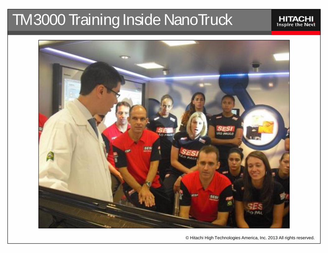
NanoTruck for Brazilian Education Outreach
© Hitachi High Technologies America, Inc. 2013 All rights reserved.
TM3000 Training Inside NanoTruck

© Hitachi High Technologies America, Inc. 2013 All rights reserved.
Inside Senai Brazil Nano Truck

© Hitachi High Technologies America, Inc. 2013 All rights reserved.
1) Choose a topic general subject of inquiry
2) Develop a question “If I make a change in X, what will happen to Y?”
3) Plan an investigation think carefully about the sort of equipment and materials needed to investigate the research question
4) Predict an outcome this is not a hypotheses
5) Experiment and observe WRITE THINGS DOWN in lab notebook
6) Interpret resultstabulating, averaging, graphing
7) Communicate findingsposter, oral presentation
7 Steps of Science Inquiry

© Hitachi High Technologies America, Inc. 2013 All rights reserved.
Eye of George Washington
Student SEM Powerpoint

© Hitachi High Technologies America, Inc. 2013 All rights reserved.
Actual Size 50x magnification
500x magnification 5000x magnification
My sample was a circuit. There were several interesting objects within the circuit.One interesting detail was the group of lines that at first appear as a solid block. As seen in the 50x image, the solid block of lines is about 300 microns thick. However,
when you magnify it further, you can see that the block of lines is not solid. There are6 micron wide lines with 1 micron spacing in between them. I learned a lot by operating
the SEM. It was a great experience and I hope to use it again.
Student SEM Powerpoint

© Hitachi High Technologies America, Inc. 2013 All rights reserved.
ßPeach
50xà
ß500x
5000xà
I put a small sliver of peach skin under the microscope to see what the “fuzz” was and to look at the skin’s features.
Taking a closer look at a peach skin, we can see that the “fuzz” is really tiny hair-like strands that are about 40 µm tall and roughly 5-10 µm in diameter.
I learned that there is more on a surface then what we first think and only by using advanced technology can we even begin to explore this world.
Student SEM Powerpoint

© Hitachi High Technologies America, Inc. 2013 All rights reserved.
Paper
TM3000 Imaging

© Hitachi High Technologies America, Inc. 2013 All rights reserved.
Band-Aid
TM3000 Imaging

© Hitachi High Technologies America, Inc. 2013 All rights reserved.
Razor Edge
TM3000 Imaging

© Hitachi High Technologies America, Inc. 2013 All rights reserved.
Fly Wing and Eye
TM3000 Imaging

© Hitachi High Technologies America, Inc. 2013 All rights reserved.
Butterfly Wing
TM3000 Imaging

© Hitachi High Technologies America, Inc. 2013 All rights reserved.
These tiny structures allow plants to take in and release gases which achieves
photosynthesis.
Stoma (Stomata)
TM3000 Imaging

© Hitachi High Technologies America, Inc. 2013 All rights reserved.
Flower Stamen and Pollen
TM3000 Imaging

© Hitachi High Technologies America, Inc. 2013 All rights reserved.
Gecko Skin
TM3000 Imaging

© Hitachi High Technologies America, Inc. 2013 All rights reserved.
Cat Hair and Dander
Are you allergic to cats? This is the dander that
makes you sneeze!
TM3000 Imaging

© Hitachi High Technologies America, Inc. 2013 All rights reserved.
Inside of a Smart Phone
TM3000 Imaging

© Hitachi High Technologies America, Inc. 2013 All rights reserved.
Salt (NaCl)
TM3000 Imaging

© Hitachi High Technologies America, Inc. 2013 All rights reserved.
Sugar
TM3000 Imaging

© Hitachi High Technologies America, Inc. 2013 All rights reserved.
EDS Elemental Analysis

© Hitachi High Technologies America, Inc. 2013 All rights reserved.
EDS Elemental Analysis

© Hitachi High Technologies America, Inc. 2013 All rights reserved.
STEM Education Website

www.inspireSTEMeducation.us | 41
• Educators are able to request 3 actions when visiting the site:
• Request Access: This gives the user additional information including lesson plans, images, abstracts and teaching tools.
• Request a Learning Lab: This will send a request to HTA where we will further coordinate with the educator to bring an instrument to the school for hands-on learning.
• Request a Speaker: This will send a request to HTA where we will coordinate an on-site visit to speak to the students and educators about STEM Education.

www.inspireSTEMeducation.us | 42
Our mission is to inspire the next generation of innovative pioneers through the advancement of Science, Technology,
Engineering, and Mathematics. Together we work with Change The Equation and The National Nanotechnology
Infrastructure Network to promote STEM education nationally.

www.inspireSTEMeducation.us | 43
Materials and resources are created and made available to educators across the country to help them teach STEM Education
in the classrooms. Lesson plans and curriculums are being continually updated as TM3000 is installed in classrooms to
stimulate learning. Once educators request access to the site, they are able to download the lesson plans freely to implement into
their course material.

www.inspireSTEMeducation.us | 44
People interested in seeing the TM3000 in action can view upcoming events where TM3000 will be displayed.


Ql We use tni cut or scro.tc~ when we nave ourselves.
Q3 This red del" . ' summer fruJ IC10US pies and . t makes Jam&.
Q2 We use th" something. IS when we write
Q4 You know fin. It looks this big fish by Its covering is t ~ooth, but this ougn armor.
Answ.n t a the bott om of page lO.
.Hitachi Hlgh-li echnologles Co rporatlon
' __ _...--'A
Hitachi HighT«h HrmcHI

1
J;l~tg~ gfiJ tbA gl_~~fiJjQIJ JDj~Jji§,€Q~~ How were microscopes invented?
Microscopes that U5e light, from the sun for example, are called optica~ microscopes. Light acts like waves. Waves have o. wavelength (the dlsto.nc~ I between the waves). Sunlight contains a mixture of light with different wavelengths. The light that our eyes can see is called visible light. Optical microscopes U5e visible light to illumincste the object.
Optical microscopes were invented arcund 1590. Dutchman Hans Janssen and his son Z4charias Janssen disc;(Wered that you ccsn make something look bigger if you combine two CQrW&X lenses. This discovery triggered the development of the first optic41 microscope. Then, in the 17th Century, Robert Hooke in Englcsnd published drawings of cork cells and microorganisms as seen through o. microscope. At that t ime microscopes could only magnify things up to 150 times in size.
If you want to see objects that are smaller than the things you can see with an optical microscope, you need to have a microscope thClt U5es something with a wavelength that Is shorter than visible light. In 1924, scientists proved that electrons act like waves, jU5t like light. Then in 1926, Hans Busch of Gennany discovered that magnetic or electrical fields could act like a lens and bend electron beams, just like an optical lens bends light.
This disccMty led the way to the invention of the electron microsc:ape, using electrnns instead of light becelUM electrons helve a shorter wavelength than visible light.
The first electron microscope was invented in 1931 by Max Knoll and Ernst RU5ka at tha Technical University of Berlin In Genncmy. Ruska than went on to Invent an electron microscope with even better ~ity. He was awarded the Nobel Prlz.e In Physics In 1986 because of this research.
How big are things at the micro level?
1m (meter)
Microwaves (microwave oven)
1mm (millimeter)
You all know what the word "mil II" meeln&, right? Mllll means one thousandth of something, so 1 millimeter Is one thoU5andth of a meter. Micro means one thousandth of a millimeter.
I Infrared rays Ultraviolet rays Electron
beam Visible light rays
11Jm (micrometer)
1nm (nanometer)
1/1,000,000 1/1,000,000,000
We basically use meters (m) to describe the length of thing&. A micrometer means Ofl8 millionth of a meter and a nanometer means one billionth of o. meter. It is difficult to imagine how small these things are.
Lets look at an axampte. If we 54Y 1m is the size of the earth (diameter: lZ,OOOkm = 1.Z billion em), then lnm would be the siz.e of a marble (diameter. 1.2cm). That is how small a nanometer is.

~tumJ rom-~~ gu@; b..@l'~fW! ibJ I.Qf§) gfi/ WA~
This is the smallest diamond ring in the world (5 millionths of a meter) as seen through an electron microscope. Electron microscopes are useful to see manufactured products at this micro level or to make sure things are of good quality.
Electron microscopes have been very helpful in the development of medicines when new viruses are discovered, to watch cells growing, or when making new biological discoveries.
Electron microscopes are used for research in ragweed or :Japanese cedar pollen that cause hay fever, and research into the body's tissues.
Electron microscopes have helped us to see the bird flu virus and norovirus
Several years ago, many people were infected by the bird flu virus or norovirus and these viruses became a major threat. The viruses that cause these diseases are only 3D-150nm in size {1nm = 1 billionth of a meter), so they can only be seen using an electron microscope. When the disease SARS spread, mainly in China, in 2003, electron microscopes helped scientists to confirm that a new type of coronavirus caused this highly dangerous disease. Now scientists are investigating new treatments and medicines. Electron microscopes are therefore important as they help scientists to develop new medicines.
Hong Kong flu (influenza A virus)
More infectious than a normal cold
-.A:i:~ovirus
.... •• • ~ A type of virus
that can cause conjunctivitis and pneumonia
~orovirus
A type of virus that can cause acute gastroenteritis
Pnoto: Dr. Etsuko Utagawa, Senior Researcher, Department of Virology II, National Institute of Infectious Diseases

5
...... ) ..,( ~ •••• ...
Diatom All diatoms photosynthesize and have one or several chloroplasts
in their cells. You cannot tell from this black and white picture, but the diatom has a green body.
Sunflowe pollen There are lots like a sea urchin! .... ~• -~• designed to stick easily .
The little ovals may look like a bumper crop of potatoes but are actually starch. Potato starch is used to keep baked goods soft and is also used in papermaking as an adhesive and coating.
Ant The v-shaped bent antennae are really important. Ants live in the dark soil and
use their antennae to identify different smells. Based on the smell, they know what is out there and where things are located.
Hair With the naked eye, a hair just looks like a single strand. When we look at
a healthy strand of hair using an electron microscope, we can see the cuticle that looks like fish scales.
Ei

7
The beautiful world of nanoArt• as seen
These are photographs of objects seen using an electron microscope. What do you see?
through electron microscopes NanoArt® involves using electron signals to create black and white images that capture the beauty within metals, minerals, or living things and then turning these into gorgeous photographs by applying colors using computer graphics technology.
This looks like a butterfly fluttering through a field of grass. The picture is actually calcium sulfate as seen through an electron microscope. Calcium sulfate is used in chalk and other substances.
This looks like a tree in a snowy field supported by ropes. This photograph is actually of a fungus that grows when it rains a lot.
This looks like J"upiter in the front and the sun at the back, right? It is actually a combination of 200 pictures of bismuth oxide particles, which are used in glass. Amazingly, the tiny world as seen through the microscope looks like outer space!
This one looks like a small frog in water, but it is actually small bumps sticking out of the cell wall of plant plankton called a diatom. The frog's face and legs are made up of different types of bumps and the artist has combined images of these different bumps to make a cute frog.
This is a diffraction image of oxides as seen through an electron microscope. The electron beam passing through the crystals produces a brilliant picture just like a firework display.
This looks like the ocean floor in a beautiful tropical sea. When looking at things through an electron microscope, scientists sometimes freeze the object being studied. This picture shows the ice that has formed on the surface of a frozen sample. Isn't it interesting that the ice looks like a tropical sea?
*
Micro Bouquet (2009)
The pretty colors look like a bunch of flowers. This is actually a picture of a synthetic zeolite. There are lots of holes on the zeolite surface, which can be used to clean smells and water. The picture looks like flowers with many layers of petals, just like real roses.
This looks like a photograph of a bridge lined with gaslights. The gaslights are only 15}.11Tl tall (0.015mm)! They are made of silicon wafers that have been processed using a special machine. The artist made the picture look like the Bandai Bridge that crosses the Shinano River in Niigata. J"apan.
* Silicon wafer: The metalloid silicon is used to make the integrated chips found in mobile phones and other devices. A silicon wafer is made of silicon cut into a very thin disk shape.
* You can see more nanoArt• here: http:/ /www.hitachi-hitec.com/global/em/nanoart/index.html * nanoArt® is a registered trademark of
Hitachi High-Technologies
8

!3
What are electrons?
Electrons are particles (the smallest units making up substances) that rotate around an atomic nucleus (the heart of the atom, which makes up matter) and also flow along electrical circuits. Electrons are so small we cannot see them and they have energy called an electric charge. Electrons have a negative charge.
What is an atom?
Negatively charged electrons are attracted to things with a positive charge. The atomic nucleus has a positive charge, so electrons are drawn towards the atomic nucleus. This force makes the electron rotate around the atomic nucleus. This combination of an atomic nucleus and electrons makes up an atom. An atom is the smallest unit of matter.
What is a virus?
•Visible to the naked eye: 0.2mm •Bacteria: 1-S.um
(,um: one millionth of a meter) •E. coli: 2,um •Visible with an optical microscope: 200nm
(nm: one billionth of a meter) •Yellow fever virus: 40-SOnm •Norovirus: 25-3Snm
A virus is a disease-causing agent that lives and replicates by taking over the cells of other living things. Viruses are only between several dozen and several hundred nanometers in size (nanometer: one billionth of a meter).
Viruses are smaller than bacteria, which are 1-S.um in size (micrometer: one millionth of a meter). Almost all viruses are smaller than 300nm, so they can only be seen using an electron microscope.
What does wavelength mean?
Wavelength describes the distance between electromagnetic waves (radio waves, infrared rays, visible light rays, ultraviolet rays). For example, light acts like waves and the distance between each wave valley (or between each wave peak) is called the wavelength. Visible light in the electromagnetic spectrum refers to the light that we can see (the colors we can detect) and has a wavelength of between 0.4,um and 0.8,um. We cannot see light with a wavelength longer or shorter than this.
Why do electron microscopes take black and white pictures? Unlike the optical microscope that produces magnified images using visible light (that we can see), an electron microscope uses an electron beam to produce a magnified image of something. An electron beam has a shorter wavelength than visible light and we cannot see the color of an electron beam, so the pictures come out black and white.
What does resolution mean?
~A Resolution describes the shortest distance between two neighboring points that allows us to see them as two separate points. Resolution gets better as this distance gets smaller. Therefore, we can see smaller things as resolution increases. --
n