Embed Size (px)
Citation preview

Highly Conductive and Low Cost Ni-PET Flexible Substrate forEfficient Dye-Sensitized Solar CellsHaijun Su,*,†,‡,∥ Mingyang Zhang,†,∥ Ya-Huei Chang,† Peng Zhai,† Nga Yu Hau,† Yu-Ting Huang,†
Chang Liu,† Ai Kah Soh,†,§ and Shien-Ping Feng*,†
†Department of Mechanical Engineering, The University of Hong Kong, Hong Kong‡State Key Laboratory of Solidification Processing, Northwestern Polytechnical University, Xi’an, 710072 Shaanxi, P. R. China§Monash University Sunway Campus, 46150 Petaling Jaya, Selangor, Malaysia
*S Supporting Information
ABSTRACT: The highly conductive and flexible nickel-polyethyleneterephthalate (Ni-PET) substrate was prepared by a facile way includingelectrodeposition and hot-press transferring. The effectiveness was demon-strated in the counter electrode of dye-sensitized solar cells (DSSCs). The Nifilm electrodeposition mechanism, microstructure, and DSSC performancefor the Ni-PET flexible substrate were investigated. The uniform and con-tinuous Ni film was first fabricated by electroplating metallic Ni on fluorine-doped tin oxide (FTO) and then intactly transferred onto PET via hot-pressing using Surlyn as the joint adhesive. The obtained flexible Ni-PETsubstrate shows low sheet resistance of 0.18Ω/□ and good chemical stabilityfor the I−/I3− electrolyte. A high light-to-electric energy conversion efficiencyof 7.89% was demonstrated in DSSCs system based on this flexible electrodesubstrate due to its high conductivity, which presents an improvement of 10.4% as compared with the general ITO-PEN flexiblesubstrate. This method paves a facile and cost-effective way to manufacture various metals on a plastic nonconducive substratebeneficial for the devices toward flexible and rollable.
KEYWORDS: flexible substrate, counter electrode, electrodeposition, conductive, photovoltaic, dye-sensitized solar cell
1. INTRODUCTION
As a promising alternative for next generation of renewablegreen energy, dye-sensitized solar cells (DSSCs) have attractedgreat attention due to their low cost, environmental friend-liness, simple fabrication, great potential of miniaturization, andportability,1−4 as well as the recent high power conversionefficiency up to 12% on fluorine-doped tin oxide (FTO) glasssubstrates.5 In general, DSSCs are composed of transparentconductive oxide (TCO) glass substrates, dye-sensitized TiO2thin film, liquid redox electrolyte, and platinum (Pt) counterelectrode (CE),1 in which the TCO glass substrates extremelyaccount for the cells volume, weight, and cost (∼60%).6Moreover, as noted, TCO glass is fragile and rigid, whose shapegreatly limits its roll-to-roll mass production. As a result, towardthe future where DSSCs go rollable and lightweight,7,8 indiumtin oxide (ITO) fabricated on plastic substrate has been widelydeveloped.4,8,9 Contrary to the rigid glass substrate, the poly-meric substrates, such as polyethylene naphthalate (PEN) andpolyethylene terephthalate (PET), cannot withstand the hightemperature so that ITO has to be coated by using RF or DCmagnetron sputtering at low temperature (<150 °C).8,10,11
Consequently, the ITO-PEN generally presents a relatively highsheet resistance (15−30 Ω/□) and poor wettability,8 de-grading the performance of flexible DSSCs. Additionally, thefabrication process of ITO substrate is time-consuming and
requires costly vacuum equipment.12−14 Accordingly, a cost-effective flexible substrate, which possesses low sheet resistance,economic efficiency, good chemical stability, and high electro-catalytic activity for the reduction of the I3
−/I− redox couple,will be greatly beneficial to facilitate DSSCs toward flexible androllable.15−17
Many groups have devoted their efforts to reduce thepreparation cost of currently used ITO-PEN or develop a newflexible substrate.18−25 Recently, the low temperature solution-based processes to fabricate ITO film on plastic substrates havebeen developed,18−21 but the resistance is relatively high dueto the unavoidable impurities remaining in the finished layer.As compared with ITO, metal films have superior conductivity.Therefore, the aqueous methods to coat metal thin film onplastic substrates present greater potentials due to their lowcost and low resistance, thereby attracting considerable researchinterest.22−26 Takehiro et al. fabricated a conductive substrateby using the self-assembly of Ag nanowires in a bubble tem-plate.24 Chen et al. coated Ag thin films on PET sheets byinkjet-printing a self-reduction silver ink synthesized by silverammonia solution mixed with diethanolamine (DEA).25
Received: December 30, 2013Accepted: March 26, 2014Published: March 26, 2014
Research Article
www.acsami.org
© 2014 American Chemical Society 5577 dx.doi.org/10.1021/am406026n | ACS Appl. Mater. Interfaces 2014, 6, 5577−5584

However, their applications as a flexible counter electrodesubstrate in DSSCs have not been reported. Moreover, thefabrication processes involve many steps, and silver is easilydissolved into the iodide-based electrolyte.27 Recently,graphene has been studied to replace Pt-based flexible CEsbut requires a costly fabrication process. In addition, the reduc-tion electrocatalytic activities of the flexible graphene-basedCEs still cannot match up to those of Pt so that limits theirfurther applications.28,29
In this work, we therefore aim to develop a highly conductiveand flexible Ni-PET substrate prepared by a facile solutionelectrodeposition and film-transferring approach, which isdemonstrated as a flexible substrate in DSSCs CE. Ni-PEThas a high electrical conductivity, good chemical stability, andlow cost30 as well as good flexibility. The polyvinylpyrrolidone(PVP)-capped Pt nanoparticles (PtNPs) were coated on theNi-PET substrate by a two-step dip coating process at lowtemperature to fabricate highly conductive PtNPs/Ni-PET CE.The DSSCs with the Ni-PET substrate show a superior energyconversion efficiency of 7.89% compared to the general ITO-PEN substrate and the rigid FTO substrate. The developedmethod is expected to provide a cost-effective and high-performance flexible substrate to facilitate DSSCs towardflexible, rollable, and lightweight.
2. EXPERIMENTAL SECTION2.1. Preparation of Conductive Ni-PET Flexible Substrate.
The FTO glasses with size of 1 × 3 cm2 (7Ω/□, 2.2 mm thick,Pilkington) were ultrasonically cleaned in 4% glass cleaner (PK-LCG545, Parker) at 50 °C for 30 min, followed by rinsing withdeionized water. The electrodeposition of Ni was carried out in astandard three-electrode system by using the FTO glass as the workingelectrode, a clean Pt mesh as the counter electrode, and an Ag/AgClelectrode as the reference electrode. Nickel was then electroplatedonto the Bepop mask (Max, CM-200E) covered FTO glass under aconstant operating voltage (−2 V) from a commercial electrolyte(Electroless Nickel Jumbo Kit, CASWEL) at 53 °C.29 Meanwhile, PET(200 μm thick, XinRuiDa) plastic with the size of 1.5 × 2 cm2 wascleaned, dried, and then treated by UV ozone (350 nm, TK-110-H01,Kingo). The Ni-PET flexible substrate was then obtained bytransferring the electroplated Ni film from FTO to the PET surfacevia hot pressing under 140 °C for 30 s using a Surlyn (Surlyn 1706,DuPont) as the joint adhesive, as schematically shown in Figure 1.
Two holes with diameters of 0.5 mm were drilled by a drilling machineso as to inject an electrolyte during DSSCS assembly.
2.2. Preparation of Flexible PtNPs/Ni-PET CE. A two-step dip-coating process was utilized to prepare PtNPs/Ni-PET CE. Ni-PETwas first immersed in a 1% conditioner solution (ML-371, OMGroup) for 5 min at 60 °C to change the surface charge state of thesubstrate to facilitate PtNPs adsorption and then was treated in PVP-PtNPs suspension (250 ppm, ACROS) for 10 min at 40 °C to form athin catalytic Pt layer. The preparation of PVP-PtNPs solution canrefer to our previous paper.31 After each step, the substrate was rinsedwith deionized water and dried using high-pressure nitrogen. UV(275W, TK-110-H01, Kingo) was used for 10 min to decompose thecapped PVP to obtain PtNPs/Ni-PET CE. As the references, thePtNPs/FTO glass CE and PtNPs/ITO-PEN flexible CE were alsoprepared with the same method for the comparison.28
2.3. Fabrication of DSSCs. The 1.5 cm × 1.5 cm FTO glass(10Ω/□, 3.1 mm thick, Nippon Sheet Glass) was used as thephotoanode substrate. The commercial nano-TiO2 paste (particle size20 nm, Eternal) was coated on the cleaned FTO glass by screenprinting to form a film with 10 μm thickness, and then a 4 μm TiO2film was printed on it as a light scattering layer using another TiO2paste (PST400, CCIC). The resulting TiO2 bilayer film was sintered at450 °C for 30 min to remove the organics and then slowly cooled toroom temperature. Subsequently, the sintered TiO2 photoanode wasimmersed in a 0.4 mM N719 dye solution (Solaronix) at roomtemperature for 12 h in order to sufficiently absorb dye molecules,followed by rinsing with ethanol and drying in air. The DSSCs werefabricated by sandwiching TiO2 photoanode (FTO-based) and flexiblePtNPs/Ni-PET CE with an electrolyte (0.2 M PMII, 0.05 M I2, 0.1 MLiI, 0.2 M TBAI, 0.5 M, TBP in AN/VN) using a 25 μm thick thermal-plastic Surlyn spacer (SX1170-25, Solaronix). The active area of thecells is 0.16 cm2. Finally, the injection holes were hot sealed using apiece of thin cover glass with a hot-melt film underneath as anadhesive. For comparison purposes, the DSSCs based on PtNPs/FTOCE and PtNPs/ITO-PEN CE with the same photoanodes wereassembled.
2.4. Characterization. The voltage and current of Ni depositionwas determined by measuring the linear sweep voltammetry (LSV)from −0.5 to −2.5 V at a scanning rate of 5 mV/s. The Ni platingcurrent versus time (chronoamperometry) at constant voltage wasmeasured. The surface morphology and composition of the as-platedNi and PtNPs/Ni-PET were investigated by field-emission scanningelectron microscope (SEM, S-4800, Hitachi) and energy dispersiveX-ray spectrometer (EDS). The four-point probe method was used tomeasure the surface resistance. The electrochemical impedance spec-troscopy (EIS) was measured by scanning the symmetric dummy cell(CE/electrolyte/CE) with a potentiostat (CHI 660E) from 100 kHzto 0.1 Hz with 5 mV amplitude at open-circuit conditions. Thephotocurrent−voltage (J-V) curves of DSSCs were recorded with acomputer-controlled digital source meter (Keithley 2400) underexposure of a standard solar simulator (PEC-L01, Pecell) under 1 sunillumination (AM 1.5G, 100 mW cm−2) based on four cells for eachcondition.
3. RESULTS AND DISCUSSION
3.1. Electrodeposition Behavior of Nickel Films onFTO. It is known that the electroplating is a simple and cost-effective method to prepare metallic film on the conductivesubstrate, which has been widely used in various fields. Ni is ahighly conductive metal commonly used in microelectronic andoptoelectronic devices. It has been reported that Ni also hashigh stability against corrosive liquid electrolyte when used inthe DSSCs.32,33 However, the PET plastic is nonconductive,which is not allowed to directly deposit Ni particles on it. Toresolve this issue, a facile approach including electrodepositionand film-transferring was used, which first obtained a metallicfilm on a FTO substrate and then transferred the metallic filmonto the PET substrate. As noted, different from the common
Figure 1. The schematical process flow for fabrication of a conductiveNi-PET flexible substrate. (a) A FTO glass was ultrasonically in glasscleaner and rinsed with deionized water; (b) The metallic nickel layerwas electroplated on FTO glass; (c) The electroplated Ni film wastransferred to a PET surface by hot-pressing, and Surlyn was worked asthe joint adhesive, creating the Ni-PET layer on the FTO substrate(d); (e) The Ni-PET substrate was removed from the FTO substrateto obtain a conductive Ni-PET flexible substrate.
ACS Applied Materials & Interfaces Research Article
dx.doi.org/10.1021/am406026n | ACS Appl. Mater. Interfaces 2014, 6, 5577−55845578

electrodeposition,34 it requires a dense Ni film having arelatively poor adhesion on FTO so as to peel off the intact Nifilm from FTO surface. In this case, the nucleation process ofelectroplated nickel on FTO is of importance to determine theNi film quality and its adhesion.Figure 2a shows the typical LSV curves of Ni electroplated
on Ni and FTO substrates from commercial Ni electrolyte at53 °C based on a potential scan rate of 5 mV/s. During theelectroplating process, the film generally undergoes theprocesses of nucleation (due to deposition potential) andgrowth (due to current density). As seen, the I−V curve ofnickel on the FTO glass presents a more negative shift(−0.8 V) than the Ni plate (−0.4 V), which indicates that thenickel electrodeposition onto the FTO surface requires a highernucleation energy. This means that the films deposited on FTOprefer to form poor adhesion than on the Ni plate, which ismore favorable to later film-transferring. The chronoampero-grams (Figure 2b and c) display the current response at anoptimized operating voltage of −2 V for Ni electroplated on Niand FTO. As seen, the current response of electroplating Ni onNi is correlated with the Cottrell equation, which reveals acertain amount of nucleation sites are rapidly generated in thevery beginning and then gradually reach a diffusion control(Figure 2b). In the case of electroplating Ni on FTO, thecurrent response increases at an initial few seconds and thenreaches a plateau (Figure 2c). As noted, the current density ofelectroplating Ni on FTO is about two times lower than that onNi. The reason is that the relatively poor wettability (lowsurface energy) of FTO leads to a higher nucleation energy so
that Ni atoms are more preferably bound to each other than tothe FTO surface.35 As shown in Figure 2d, the initial transientportions of the experimental data were analyzed in i vs t1/2 plotfor the characterization of instantaneous nucleation, while i vst3/2 plot in the inset for the progressive nucleation. A goodlinearity in i vs t1/2 plot indicates that an instantaneous nuclea-tion occurs when electroplating Ni on FTO. In the case ofinstantaneous nucleation, the nuclei density is almost the sameas the initial nuclei density (N0), which can be calculated basedon the following equation36
π ρ= −N CM zFC i t0.065(8 / ) [ /( )]01/2
max max2
(1)
where C is the metal ion concentration in the solution, zF is themolar charge transferred during electrodeposition, imax is thepeak current density, tmax is the peak time, and M and ρ aremolecular weight and density of the deposited material,respectively. The calculated nuclei density of nickel on FTOis around 1.7 × 107 cm−2, which is much smaller than thegeneral value of the nuclei density (∼109 cm−2) for electro-plating Ni on metal substrates.37 The average rate of Ni filmdeposition on FTO is about 0.8 μm/min based on themeasured film thickness by the α-step method (Figure S1).Figure 3 shows the SEM microstructure morphology of
electroplated nickel on a blank FTO at −2 V for different initialelectrodeposition times of 0, 0.25, and 0.5 s. As seen, the blankFTO glass exhibits an uneven and random distribution of tinoxide grains with an obvious grain boundary and irregular shapeand large size (Figure 3a). After an instantaneous deposition of0.25 s, spherical Ni nuclei with a adiameter size of about 40 nm
Figure 2. Linear sweep voltammetry for Ni electroplated on a Ni plate and FTO at a potential scan rate of 5 mV/s (a); Chronoamperograms ofelectroplating Ni on a Ni plate (b) and FTO (c) under an operating voltage of −2 V; (d) Dependence of i vs t1/2 plot for the initial transient portionof Ni electroplated on FTO. The inset shows the dependence of i vs t3/2 plot.
ACS Applied Materials & Interfaces Research Article
dx.doi.org/10.1021/am406026n | ACS Appl. Mater. Interfaces 2014, 6, 5577−55845579

have been formed (Figure 3b). With further increasing thedeposition time (Figure 3c), it is found that the number ofnucleation sites does not increase, but the sizes of particlesincrease and the distributions of size and shape become uneven.In this stage, the formation of Ni nuclei has finished, and Nigrain begins to grow, of which the growth rate is determined bythe operating current. As mentioned, the early stage of theelectrochemical phase transformation corresponds to aninstantaneous nucleation model, where the growth of nucleion a small number of active sites, such as atomic step, grainedge, crystal defects, and impurities,31 occurs in a very shorttime period. These nucleation sites grow into islands and thencoalesce (Volmer−Weber growth).38,39 Island growth duringelectroplating nucleation is usually not desirable fortechnological applications due to its poor adhesion. Here, incontrast, we utilized this unique property to transfer the intactNi film from FTO to PET via hot-pressing with the aid ofSurlyn as a joint adhesive. The peel-off test demonstrates thatthe nickel film can be simply and intactly detached from FTO byan ordinary tape due to its weak interfacial adhesion, as seen inFigure 4.3.2. Characterization of Ni-PET and PtNPs/Ni-PET
Substrates. Figure 5a shows the SEM microstructuremorphology of the obtained flexible Ni-PET. The compositionof the film is characterized by EDS (Figure S2) and listed inTable 1. As seen, the morphology of the Ni surface is an inversemorphology of the FTO surface because electroplated Ni wasgrown along with FTO. It provides a microroughness Nisurface which is beneficial to the subsequent two-step PVP-PtNPs dip-coating process.10 As shown in Figure 5b, the Ptnanoclusters are homogeneously distributed on the surface ofNi-PET. Compared with PtNPs/FTO and PtNPs/ITO-PEN
using the same coating process (Figure S3), the relatively highPt loading of 1.64 wt % can be achieved in PtNPs/Ni-PET(Table 1). Moreover, no significant carbon impurity was foundon PtNPs/Ni-PET (Figure S4), revealing that most of PVP canbe completely decomposed by UV treatment.As mentioned, Surlyn plays an important role to joint Ni and
PET together via hot pressing. In this sandwich scheme, theadhesion between Surlyn and PET is not as good as thatbetween Surlyn and Ni, causing a localized peeling underbending deformation, as shown by the red circles in Figure 6a.To solve this problem, UV ozone treatment was employed tomodify the PET surface before hot pressing to enhance theinterfacial bonding. Figure 6b shows no obvious peeling orcracks occurring under bending deformation. The sheetresistance of the Ni-PET substrate is 0.18 Ω/□ measured by
Figure 3. SEM images showing the microstructure morphology of electroplated nickel on blank FTO at an initial deposition time of 0 s (a), 0.25 s(b), and 0.5 s (c) at an operating voltage of −2 V.
Figure 4. Typical photograph (a) of electroplated nickel on blankFTO at an operating voltage of −2 V for 60 s. (b) Showing the film iscompletely peeled off by the tape.
ACS Applied Materials & Interfaces Research Article
dx.doi.org/10.1021/am406026n | ACS Appl. Mater. Interfaces 2014, 6, 5577−55845580

the four-point probe method, which is obviously superior toFTO (10 Ω/□) and ITO-PEN (15−30 Ω/□).40 This resultindicates that the obtained Ni-PET film possesses highconductivity and good bending characteristics, which is suitableto be used as DSSCs CE.3.3. Photovoltaic Performance of DSSCs. The interfacial
electrochemical behaviors between flexible Pt/Ni-PET CEs andelectrolytes are determined by a two-electrode EIS system. Forcomparison purposes, three kinds of CEs (PtNPs/Ni-PET,PtNPs/ITO-PEN, PtNPs/FTO) were investigated. Here, theseeletrodes were all assembled with another PtNPs/FTO andthereby formed the symmetric (PtNPs/FTO vs PtNPs/FTO)or the asymmetric (PtNPs/Ni-PET vs PtNPs/FTO or PtNPs/ITO-PEN vs PtNPs/FTO) two-electrode dummy cells. TheNyquist plots of three dummy cells are shown in Figure 7a.The equivalent circuit is depicted in the inset of Figure 7aincluding series resistance (Rs) in the high-frequency region,charge transfer resistance (Rct) and double-layer capacitance(Cct) in the middle frequency region, and electrolyte diffusionresistance (Zw) in the low frequency.41 Resistance contributionof each CE in the symmetric cell (FTO/FTO) can be simplydivided by two, while that in the asymmetric cases (Ni-PET/
FTO, ITO-PEN/FTO) should be obtained by subtracting theresistance of single PtNPs/FTO from the total resistance. Thefitted data based on this model is summarized in Table 2. Asseen, PtNPs/Ni-PET CE shows a much smaller Rs of 0.23 Ωthan PtNPs/FTO CE of 7.48 Ω and PtNPs/ITO-PEN CE of12.94 Ω, which is mainly attributed to the low sheet resistanceof the Ni film. The great decrease of Rs is beneficial to enhancethe electron transportation ability and thereby to improve thefill factor of DSSCs.42Based on the first semicircles (Figure 7a),the charge transfer resistances for these CEs are almost thesame, indicating the similar electrochemical catalytic activityto the I3−/I− redox reaction. The electrolyte diffusion resistance(Zw) represented in the second semicircles shows a slightincrease in PtNPs/Ni-PET CE compared to its counterpartspossibly due to the localized relative long diffusion distancecoming from the inverse FTO microstructure (see Figure 5).Meanwhile, the catalytic peaks (Figure 7b) for three counterslie at the same frequency, revealing that the flexible Pt/Ni-PETCE performs a good catalytic activity comparable to Pt/FTOCE and Pt/ITO-PEN CE. Moreover, the corresponding Bode
Figure 5. SEM images showing the microstructure morphology of the transferred Ni-PET film (a) and the PtNPs/Ni-PET film (b).
Table 1. Composition of Ni-PET and PtNPs/Ni-PET Films
film element weight percent (wt %) atomic percent (at %)
Ni-PET Ni 100.00 100.00PtNPs/Ni-PET Ni 98.36 99.50
Pt 1.64 0.50
Figure 6. Photographs of the transferred nickel film onto the PET substrate during bending: (a) PET without UV ozone treatment and (b) PETwith UV ozone treatment.
Table 2. Electrochemical Impedance Parameters of the Two-Electrode Configuration Based on the Ni-PET, FTO, andITO-PEN Substrates
substrate Rs (Ω) Rct (Ω) Zw (Ω)
Ni-PET 0.23 2.04 2.41FTO 7.48 2.42 1.31ITO-PEN 12.94 1.68 1.81
ACS Applied Materials & Interfaces Research Article
dx.doi.org/10.1021/am406026n | ACS Appl. Mater. Interfaces 2014, 6, 5577−55845581
plot in Figure 7b shows the same level of characteristic electronlifetime constant (τe = 1/2πf),43 indicating the same reactionrate of the I3−/I− redox reaction among PtNPs/Ni-PET CE,PtNPs/ITO-PEN CE, and PtNPs/FTO CE.
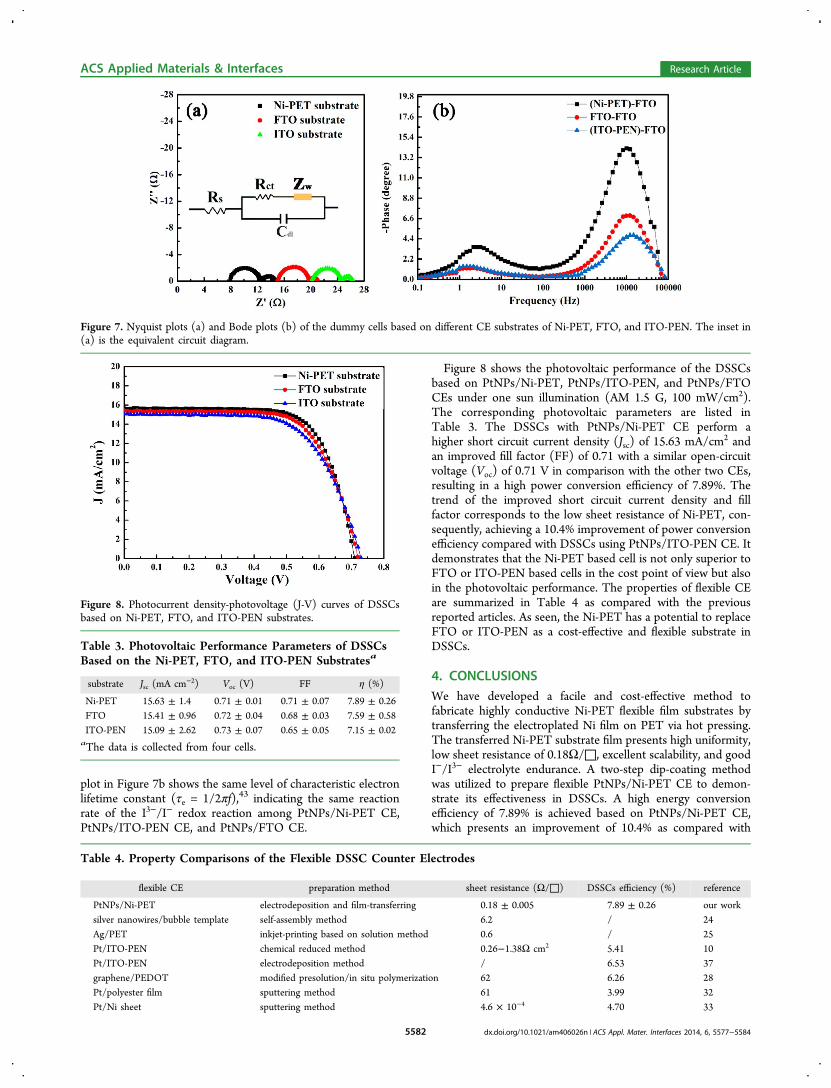
Figure 8 shows the photovoltaic performance of the DSSCsbased on PtNPs/Ni-PET, PtNPs/ITO-PEN, and PtNPs/FTOCEs under one sun illumination (AM 1.5 G, 100 mW/cm2).The corresponding photovoltaic parameters are listed inTable 3. The DSSCs with PtNPs/Ni-PET CE perform ahigher short circuit current density (Jsc) of 15.63 mA/cm2 andan improved fill factor (FF) of 0.71 with a similar open-circuitvoltage (Voc) of 0.71 V in comparison with the other two CEs,resulting in a high power conversion efficiency of 7.89%. Thetrend of the improved short circuit current density and fillfactor corresponds to the low sheet resistance of Ni-PET, con-sequently, achieving a 10.4% improvement of power conversionefficiency compared with DSSCs using PtNPs/ITO-PEN CE. Itdemonstrates that the Ni-PET based cell is not only superior toFTO or ITO-PEN based cells in the cost point of view but alsoin the photovoltaic performance. The properties of flexible CEare summarized in Table 4 as compared with the previousreported articles. As seen, the Ni-PET has a potential to replaceFTO or ITO-PEN as a cost-effective and flexible substrate inDSSCs.
4. CONCLUSIONSWe have developed a facile and cost-effective method tofabricate highly conductive Ni-PET flexible film substrates bytransferring the electroplated Ni film on PET via hot pressing.The transferred Ni-PET substrate film presents high uniformity,low sheet resistance of 0.18Ω/□, excellent scalability, and goodI−/I3− electrolyte endurance. A two-step dip-coating methodwas utilized to prepare flexible PtNPs/Ni-PET CE to demon-strate its effectiveness in DSSCs. A high energy conversionefficiency of 7.89% is achieved based on PtNPs/Ni-PET CE,which presents an improvement of 10.4% as compared with
Figure 7. Nyquist plots (a) and Bode plots (b) of the dummy cells based on different CE substrates of Ni-PET, FTO, and ITO-PEN. The inset in(a) is the equivalent circuit diagram.
Figure 8. Photocurrent density-photovoltage (J-V) curves of DSSCsbased on Ni-PET, FTO, and ITO-PEN substrates.
Table 3. Photovoltaic Performance Parameters of DSSCsBased on the Ni-PET, FTO, and ITO-PEN Substratesa
substrate Jsc (mA cm−2) Voc (V) FF η (%)
Ni-PET 15.63 ± 1.4 0.71 ± 0.01 0.71 ± 0.07 7.89 ± 0.26FTO 15.41 ± 0.96 0.72 ± 0.04 0.68 ± 0.03 7.59 ± 0.58ITO-PEN 15.09 ± 2.62 0.73 ± 0.07 0.65 ± 0.05 7.15 ± 0.02aThe data is collected from four cells.
Table 4. Property Comparisons of the Flexible DSSC Counter Electrodes
flexible CE preparation method sheet resistance (Ω/□) DSSCs efficiency (%) reference
PtNPs/Ni-PET electrodeposition and film-transferring 0.18 ± 0.005 7.89 ± 0.26 our worksilver nanowires/bubble template self-assembly method 6.2 / 24Ag/PET inkjet-printing based on solution method 0.6 / 25Pt/ITO-PEN chemical reduced method 0.26−1.38Ω cm2 5.41 10Pt/ITO-PEN electrodeposition method / 6.53 37graphene/PEDOT modified presolution/in situ polymerization 62 6.26 28Pt/polyester film sputtering method 61 3.99 32Pt/Ni sheet sputtering method 4.6 × 10⁻⁴ 4.70 33
ACS Applied Materials & Interfaces Research Article
dx.doi.org/10.1021/am406026n | ACS Appl. Mater. Interfaces 2014, 6, 5577−55845582

PtNPs/ITO-PEN CE and is also comparable to PtNPs/FTOCE. This facile and cost-effective method for fabricating theconductive flexible substrate has a great potential in the applica-tion of other flexible devices, such as organic solar cell and lightemitted diode (LED).
■ ASSOCIATED CONTENT*S Supporting InformationThickness measurement and EDS spectrum of the Ni film onPET substrates and the SEM images and EDS results of thePtNPs/Ni-PET film. This material is available free of charge viathe Internet at http://pubs.acs.org.
■ AUTHOR INFORMATIONCorresponding Authors*E-mail: [email protected] (H.S.).*E-mail: [email protected] (S.P.F.).Author Contributions∥These authors contributed equally to this work.NotesThe authors declare no competing financial interest.
■ ACKNOWLEDGMENTSThis work was supported by the General Research Fund fromResearch Grants Council of Hong Kong Special AdministrativeRegion, China, under Award Numbers HKU 717011 and HKU719512E and the Hong Kong Scholars Program Fund (No.XJ2011030).
■ REFERENCES(1) O’Regan, B.; Gratzel, M. A Low-Cost, High-Efficiency Solar CellBased on Dye-Sensitized Colloidal TiO2 Films. Nature 1991, 353,737−740.(2) Gratzel, M. Photoelectrochemical Cells. Nature 2001, 414, 338−344.(3) Gratzel, M. Recent Advances in Sensitized Mesoscopic SolarCells. Acc. Chem. Res. 2009, 42, 1788−1798.(4) Upadhyaya, H. M.; Senthilarasu, S.; Hsu, M. H.; Kumar, D. K.Recent Progress and the Status of Dye-Sensitised Solar Cell (DSSC)Technology with State-of-the-Art Conversion Efficiencies. Sol. EnergyMater. Sol. Cells 2013, 119, 291−295.(5) Yella, A.; Lee, H. W.; Tsao, H. N.; Yi, C.; Chandiran, A. K.;Nazeeruddin, M. K.; Diau, E. W. G.; Yeh, C. Y.; Zakeeruddin, S. M.;Gratzel, M. Porphyrin-Sensitized Solar Cells with Cobalt (II/III)-Based Redox Electrolyte Exceed 12% Efficiency. Science 2011, 334,629−634.(6) Wang, Y. D.; Wu, M. X.; Lin, X.; Shi, Z. C.; Hagfeldt, A.; Ma, T.L. Several Highly Efficient Catalysts for Pt-Free and FTO-FreeCounter Electrodes of Dye-Sensitized Solar Cells. J. Mater. Chem.2012, 22, 4009−4014.(7) Jen, H. P.; Lin, M. H.; Li, L. L.; Wu, H. P.; Huang, W. K.; Cheng,P. J.; Diau, E. W. G. High-Performance Large-Scale Flexible Dye-Sensitized Solar Cells Based on Anodic TiO2 Nanotube Arrays. ACSAppl. Mater. Interfaces 2013, 5, 10098−10104.(8) Weerasinghe, H. C.; Huang, F. Z.; Cheng, Y. B. Fabrication ofFlexible Dye Sensitized Solar Cells on Plastic Substrates. Nano Energy2013, 2, 174−189.(9) Gong, Y.; Li, C. H.; Huang, X. M.; Luo, Y. H.; Li, D. M.; Meng,Q. B.; Iversen, B. B. Simple Method for Manufacturing Pt CounterElectrodes on Conductive Plastic Substrates for Dye-Sensitized SolarCells. ACS Appl. Mater. Interfaces 2013, 5, 795−800.(10) Chen, L. L.; Tan, W. W.; Zhang, J. B.; Zhou, X. W.; Zhang, X.L.; Lin, Y. Fabrication of High Performance Pt Counter Electrodes onConductive Plastic Substrate for Flexible Dye-Sensitized Solar Cells.Electrochim. Acta 2010, 55, 3721−3726.
(11) Li, Y.; Cui, P.; Wang, L. Y.; Lee, H.; Lee, K.; Lee, H. HighlyBendable, Conductive, and Transparent Film by an EnhancedAdhesion of Silver Nanowires. ACS Appl. Mater. Interfaces 2013, 5,9155−9160.(12) Tuna, O.; Selamet, Y.; Aygun, G.; Ozyuzer, L. High Quality ITOThin Films Grown by Dc and RF Sputtering without Oxygen. J. Phys.D: Appl. Phys. 2010, 43, 055402.(13) David, S. H.; Richard, B. K. Solution-Processed TransparentElectrodes. MRS Bull. 2011, 36, 749−755.(14) Yun, J.; Park, Y. H.; Bae, T. S.; Lee, S.; Lee, G. H. Fabrication ofa Completely Transparent and Highly Flexible ITO NanoparticleElectrode at Room Temperature. ACS Appl. Mater. Interfaces 2013, 5,164−172.(15) Wu, M. X.; Lin, X.; Wang, T. H.; Qiu, J. S.; Ma, T. L. Low-CostDye-Sensitized Solar Cell Based on Nine Kinds of Carbon CounterElectrodes. Energy Environ. Sci. 2011, 4, 2308−2315.(16) Huang, S.; Li, L.; Yang, Z.; Zhang, L.; Saiyin, H.; Chen, T.;Peng, H. A New and General Fabrication of an Aligned CarbonNanotube/Polymer Film for Electrode Applications. Adv. Mater. 2011,23, 4707−4710.(17) Yamaguchi, T.; Tobe, N.; Matsumoto, D.; Nagai, T.; Arakawa,H. Highly Efficient Plastic-Substrate Dye-Sensitized Solar Cells withValidated Conversion Efficiency of 7.6%. Sol. Energy Mater. Sol. Cells2010, 94, 812−816.(18) Lee, J.; Lee, S.; Li, G.; Petruska, M. A.; Paine, D. C.; Sun, S. AFacile Solution-Phase Approach to Transparent and Conducting ITONanocrystal Assemblies. J. Am. Chem. Soc. 2012, 134, 13410−13414.(19) Dattoli, E. N.; Lu, W. ITO Nanowires and Nanoparticles forTransparent Films. MRS Bull. 2011, 36, 782−788.(20) Puetz, J.; Aegerter, M. A. Direct Gravure Printing of Indium TinOxide Nanoparticle Patterns on Polymer Foils. Thin Solid Films 2008,516, 4495−4501.(21) Pasquarelli, R. M.; Ginley, D. S.; O’Hayrea, R. SolutionProcessing of Transparent Conductors: From Flask to Film. Chem. Soc.Rev. 2011, 40, 5406−5441.(22) De, S.; Higgins, T. M.; Lyons, P. E.; Doherty, E. M.; Nirmalraj,P. N.; Blau, W. J.; Boland, J. J.; Coleman, J. N. Silver NanowireNetworks as Flexible, Transparent, Conducting Films: Extremely HighDC to Optical Conductivity Ratios. ACS Nano 2009, 3, 1767−1774.(23) Rathmell, A. R.; Bergin, S. M.; Hua, Y. L.; Li, Z. Y.; Wiley, B. J.The Growth Mechanism of Copper Nanowires and Their Propertiesin Flexible, Transparent Conducting Films. Adv. Mater. 2010, 22,3558−3563.(24) Tokuno, T.; Nogi, M.; Jiu, J.; Sugahara, T.; Suganuma, K.Transparent Electrodes Fabricated via the Self-Assembly of SilverNanowires Using a Bubble Template. Langmuir 2012, 28, 9298−9302.(25) Chen, S. P.; Kao, Z. K.; Lin, J. L.; Liao, Y. C. Silver ConductiveFeatures on Flexible Substrates from a Thermally Accelerated ChainReaction at Low Sintering Temperatures. ACS Appl. Mater. Interfaces2012, 4, 7064−7068.(26) Carlson, A.; Bowen, A. M.; Huang, Y. G.; Nuzzo, R. G.; Rogers,J. A. Transfer Printing Techniques for Materials Assembly and Micro/Nanodevice Fabrication. Adv. Mater. 2012, 24, 5284−5318.(27) Lee, J.; Connor, S.; Cui, Y.; Peumans, P. Solution-ProcessedMetal Nanowire Mesh Transparent Electrodes. Nano Lett. 2008, 8,689−692.(28) Lee, K. S.; Lee, Y.; Lee, J. Y.; Ahn, J. H.; Park, J. H. Flexible andPlatinum-Free Dye-Sensitized Solar Cells with Conducting-Polymer-Coated Graphene Counter Electrodes. ChemSusChem 2012, 5, 379−382.(29) Wang, H.; Hu, Y. H. Graphene as a Counter Electrode Materialfor Dye-Sensitized Solar Cells. Energy Environ. Sci. 2012, 5, 8182−8188.(30) Huang, Y. T.; Feng, S. P.; Chen, C. M. Nickel SubstrateCovered with a Sn-Based Protection Bi-Layer as a PhotoanodeSubstrate for Dye-Sensitized Solar Cells. Electrochim. Acta 2013, 99,230−237.
ACS Applied Materials & Interfaces Research Article
dx.doi.org/10.1021/am406026n | ACS Appl. Mater. Interfaces 2014, 6, 5577−55845583

(31) Feng, H. P.; Paudel, T. C.; Yu, B.; Chen, S.; Ren, Z. F.; Chen, G.Nanoparticle-Enabled Selective Electrodeposition. Adv. Mater. 2011,23, 2454−2459.(32) Ma, T.; Fang, X.; Akiyama, M.; Inoue, K.; Noma, H.; Abe, E.Properties of Several Types of Novel Counter Electrodes for Dye-Sensitized Solar Cells. J. Electroanal. Chem. 2004, 574, 77−83.(33) Fang, X.; Ma, T.; Akiyama, M.; Guan, G.; Tsunematsu, S.; Abe,E. Flexible Counter Electrodes Based on Metal Sheet and PolymerFilm for Dye-Sensitized Solar Cells. Thin Solid Films 2005, 472, 242−245.(34) Bai, A.; Hu, C. C. Effects of Electroplating Variables on theComposition and Morphology of Nickel-Cobalt Deposits Platedthrough Means of Cyclic Voltammetry. Electrochim. Acta 2002, 47,3447−3456.(35) Kaganer, V. M.; Jenichen, B.; Shayduk, R.; Braun, W.; Riechert,H. Kinetic Optimum of Volmer-Weber Growth. Phys. Rev. Lett. 2009,102, 016103.(36) Khelladi, M. R.; Mentar, L.; Azizi, A.; Sahari, A.; Kahoul, A.Electrochemical Nucleation and Growth of Copper Deposition ontoFTO and N-Si (100) Electrodes. Mater. Chem. Phys. 2009, 115, 385−390.(37) Adriana, I.; Hisayoshi, M.; Andreas, B.; Benedetto, B.Nucleation and Growth of Thin Nickel Layers under the Influenceof a Magnetic Field. J. Electroanal. Chem. 2009, 626, 174−182.(38) Fu, N. Q.; Xiao, X. R.; Zhou, X. W.; Zhang, J. B.; Lin, Y.Electrodeposition of Platinum on Plastic Substrates as CounterElectrodes for Flexible Dye-Sensitized Solar Cells. J. Phys. Chem. C2012, 116, 2850−2857.(39) Chang, H.; Chen, T. L.; Huang, K. D.; Chien, S. H.; Hung, K. C.Fabrication of Highly Efficient Flexible Dye-Sensitized Solar Cells. J.Alloys Compd. 2010, 504, S435−S438.(40) Kawashima, T.; Matsui, H.; Tanabe, N. New TransparentConductive Films: FTO Coated ITO. Thin Solid Films 2003, 445,241−244.(41) Yin, X.; Xue, Z. S.; Liu, B. Electrophoretic Deposition of PtNanoparticles on Plastic Substrates as Counter Electrode for FlexibleDye-Sensitized Solar Cells. J. Power Sources 2011, 196, 2422−2426.(42) Ikegami, M.; Miyoshi, K.; Miyasaka, T.; Teshima, K.; Wei, T. C.;Wan, C. C.; Wang, Y. Y. Platinum/Titanium Bilayer Deposited onPolymer Film as Efficient Counter Electrodes for Plastic Dye-Sensitized Solar Cells. Appl. Phys. Lett. 2007, 90, 153122.(43) Lee, K. M.; Lee, E. S.; Yoo, B. Y.; Shin, D. H. Synthesis of ZnO-Decorated TiO2 Nanotubes for Dye-Sensitized Solar Cells. Electrochim.Acta 2013, 109, 181−186.
ACS Applied Materials & Interfaces Research Article
dx.doi.org/10.1021/am406026n | ACS Appl. Mater. Interfaces 2014, 6, 5577−55845584
![Substrate and p-layer effects on polymorphous silicon solar ......by texturing of transparent conductive oxide (TCO) lay-ers on glass substrates [11]. However, this approach tends](https://img.dokumen.tips/doc/110x75/60802e6fc0b1ac7f436b0306/substrate-and-p-layer-effects-on-polymorphous-silicon-solar-by-texturing.jpg)


![Bio‐Based Transparent Conductive Film Consisting of ...homepage.ntu.edu.tw/~shtung/Publications/2018_Macromol...flexible optoelectronic devices.[1] Among which, PET, as the most](https://img.dokumen.tips/doc/110x75/613cd4514c23507cb635a1a1/bioabased-transparent-conductive-film-consisting-of-shtungpublications2018macromol.jpg)