Embed Size (px)
Citation preview

General rights Copyright and moral rights for the publications made accessible in the public portal are retained by the authors and/or other copyright owners and it is a condition of accessing publications that users recognise and abide by the legal requirements associated with these rights.
Users may download and print one copy of any publication from the public portal for the purpose of private study or research.
You may not further distribute the material or use it for any profit-making activity or commercial gain
You may freely distribute the URL identifying the publication in the public portal If you believe that this document breaches copyright please contact us providing details, and we will remove access to the work immediately and investigate your claim.
Downloaded from orbit.dtu.dk on: May 12, 2020
High-voltage integrated transmitting circuit with differential driving for CMUTs
Llimos Muntal, Pere; Larsen, Dennis Øland; Færch, Kjartan Ullitz; Jørgensen, Ivan Harald Holger; Bruun,ErikPublished in:Analog Integrated Circuits and Signal Processing
Link to article, DOI:10.1007/s10470-016-0793-2
Publication date:2016
Document VersionPeer reviewed version
Link back to DTU Orbit
Citation (APA):Llimos Muntal, P., Larsen, D. Ø., Færch, K. U., Jørgensen, I. H. H., & Bruun, E. (2016). High-voltage integratedtransmitting circuit with differential driving for CMUTs. Analog Integrated Circuits and Signal Processing, 89(1),25-34. https://doi.org/10.1007/s10470-016-0793-2

Noname manuscript No.(will be inserted by the editor)
High-Voltage Integrated Transmitting Circuit with Differential Drivingfor CMUTs
Pere Llimos Muntal · Dennis Øland Larsen · Kjartan Færch · Ivan H.H. Jørgensen ·Erik Bruun
Received: date / Accepted: date
Abstract In this paper, a high-voltage integrated differen-tial transmitting circuit for capacitive micromachined ultra-sonic transducers (CMUTs) used in portable ultrasound scan-ners is presented. Due to its application, area and powerconsumption are critical and need to be minimized. The cir-cuitry is designed and implemented in AMS 0.35 µm high-voltage process. Measurements are performed on the fabri-cated integrated circuit in order to assess its performance.The transmitting circuit consists of a low-voltage controllogic, pulse-triggered level shifters and a differential outputstage that generates pulses at differential voltage levels of60 V, 80 V and 100 V, a frequency up to 5 MHz and a mea-sured driving strength of 2.03 V/ns with the CMUT electri-cal model connected. The total on-chip area occupied by thetransmitting circuit is 0.18 mm2 and the power consumptionat the ultrasound scanner operation conditions is 0.936 mWincluding the load. The integrated circuits measured prove tobe consistent and robust to local process variations by mea-surements.
Keywords Integrated · Transmitting circuit ·High-voltage ·Pulser · Level shifter ·Output stage ·Ultrasound · Scanners ·CMUT
Pere Llimos Muntal · Dennis Øland Larsen · Ivan H.H. Jørgensen ·Erik BruunDepartment of Electrical Engineering, Electronics GroupTechnical University of Denmark (DTU)Building 325, Kgs. Lyngby, 2800 DenmarkE-mail: [email protected]
Kjartan FærchAnalogic Ultrasound, BK Medical Design CenterMileparken 34, Herlev, 2730 Denmark
1 Introduction
Ultrasound scanners are widely used in medical applicationssince it is a very effective and fast diagnostic technique. Thetraditional static ultrasound scanners are large devices whichare plugged into the grid and therefore they have no powerconsumption limitation. Consequently, the design tendencyis to keep increasing their complexity to obtain better pic-ture quality. The electronics used in static ultrasound scan-ners are typically discrete components due to their low cost.These components are over-designed and tend to consumeconsiderably more power than needed for a specific applica-tion. Nonetheless, this is not an issue due to the practicallylimitless amount of power available.
Even though static ultrasound scanners are very effec-tive, they have some drawbacks. Firstly, due to size and com-plexity, the amount of diagnosis that can be performed perunit of time is limited. Furthermore, the amount of devicesavailable per hospital is also limited by the cost per scanner.In order to overcome these drawbacks, portable ultrasounddevices are being developed. These devices have a muchlower cost and allow a significant increase in the amountof diagnosis per unit of time. However, portable scannershave power consumption, heat dissipation and area limita-tions, hence the design approach of a portable ultrasoundscanner is to utilize the power budget and area available inthe most effective way in order to achieve the best picturequality possible. The electronics for the scanner need to becustom designed requiring an application specific integratedcircuit (ASIC) solution. In the last decade, high integrationhas enabled portable ultrasound scanners to have a sufficientpicture quality, even comparable to the performance of thelow end traditional static ultrasound scanners, making themusable for medical applications.
Portable ultrasound scanners consist of hundreds of chan-nels and each of them has a transducer, a high-voltage trans-

2 Pere Llimos Muntal et al.
Fig. 1 Picture of the CMUT array.
mitting circuit (Tx) and a low-voltage receiving circuit (Rx).The Tx provides the high-voltage pulses that the transducerneeds to generate ultrasonic waves and the Rx amplifies anddigitizes the low-voltage signal induced in the transducer.There are several types of transducers, and the most com-monly used are the piezoeletric transducers. However, re-cent studies have shown that capacitive micromachined ul-trasonic transducers (CMUTs) have several advantages re-spect to the piezoelectric ones such as wider bandwidth, bet-ter temporal and axial resolution, and also better thermic andtransduction efficiency [1]. Furthermore, CMUTs have highintegration compatibility with electronics since their fabri-cation process is similar to the standard silicon processesused for integrated circuits [2].
CMUTs are composed of a thin movable plate suspendedon a small vacuum gap on top of a substrate. They have twoterminals, one connected to the substrate and the other con-nected to the movable plate. By applying a voltage differ-ence between the two terminals of the CMUT, the thin platedeflects due to an electrostatic force. The ultrasound is gen-erated when applying high-voltage pulses in one of the ter-minals of the CMUT which makes the thin plate vibrate [3].
This paper is an extended version of the work [4] pub-lished in 13th IEEE International NEW Circuits And Sys-tems (NEWCAS) conference in 2015. The transmitting cir-cuit design is a new and improved version of the work pre-sented in [5]. Due to the high-voltage necessity of the trans-ducers, the circuitry is implemented in AMS 0.35 µm high-voltage CMOS process. Designing in high-voltage processesis a challenge because of the very strict design rules in or-der to avoid breakdown voltages and the use of high-voltagedevices, which are more complex than the standard CMOSprocess ones.
Fig. 2 Transmitting circuit block structure.
2 Transmitting circuit specifications
The transmitting circuit needs to drive a particular CMUT,therefore its specifications come from the inherent trans-ducer characteristics. The CMUT used in this project hasbeen designed and modeled at Nanotech department at theTechnical University of Denmark (DTU), and even thoughthe driving requirements are described here, the electricalequivalent model of the CMUT is confidential, therefore itis not presented in this paper. A picture of several of theseCMUTs collected in an array is shown in Fig. 1. Each CMUT,which is mainly a capacitive load, has an equivalent capac-itance of approximately 30 pF and has a resonant frequencyof ft = 5MHz. In receiving mode, the transducer needs abias voltage of 80 V and during transmission, the CMUT re-quires high-voltage pulses from 60 V to 100 V toggling at itsresonant frequency and a driving strength corresponding toa slew rate (SR) of 2 V/ns. Ultrasound scanners transmit fora short period of time, 400 ns, and receive for a much longerperiod of time, 106.4 µs, hence the operation transmittingduty cycle is 1/266 in this particular application.
3 Design and implementation of the Tx
The structure of the transmitting circuit designed in this pa-per is shown in Fig. 2. The Tx consists of a three-level high-voltage output stage that drives the ultrasonic transducer,which is controlled with high-voltage signals provided bythe level shifters. The low-voltage signals needed for thelevel shifters’ operation are generated by the control logicblock. The design approach is to minimize the area and powerconsumption therefore no reconfigurability features have beenadded. The Tx is designed to drive a specific CMUT with thecharacteristics described in Section 2.
In the next subsections the design of each block of theTx circuit is presented. The MOS devices used in all theschematics are devices with different maximum drain-source(VDS,max) and gate-source (VGS,max) breakdown voltages.A summary table with the symbol of each device is shownin Fig. 3. Note that NMOSi stands for an NMOS which islocated in its own P-well, therefore its bulk terminal can betied to a different voltage potential than the p-substrate.
Fig. 3 Symbols of the transistors used in the Tx design.
High-Voltage Integrated Transmitting Circuit with Differential Driving for CMUTs 3
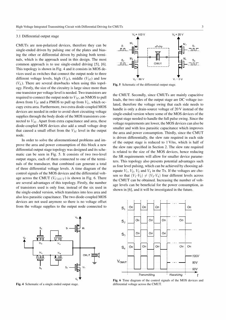
3.1 Differential output stage
CMUTs are non-polarized devices, therefore they can besingle-ended driven by pulsing one of the plates and bias-ing the other or differential driven by pulsing both termi-nals, which is the approach used in this design. The mostcommon approach is to use single-ended driving [5], [6].This topology is shown in Fig. 4 and it consists in MOS de-vices used as switches that connect the output node to threedifferent voltage levels, high (VH ), middle (VM ) and low(VL). There are several drawbacks when using this topol-ogy. Firstly, the size of the circuitry is large since more thanone transistor per voltage level is needed. Two transistors arerequired to connect the output node to VM , an NMOS to pulldown from VH and a PMOS to pull up from VL, which oc-cupy extra area. Furthermore, two extra diode-coupled MOSdevices are needed in order to avoid short circuiting voltagesupplies through the body diode of the MOS transistors con-nected to VM . Apart from extra capacitance and area, thesediode-coupled MOS devices also add a small voltage dropthat caused a small offset from the VM level in the outputnode.
In order to solve the aforementioned problems and im-prove the area and power consumption of this block a newdifferential output stage topology was designed and its sche-matic can be seen in Fig. 5. It consists of two two-leveloutput stages, each of them connected to one of the termi-nals of the transducer, that combined can generate a totalof three differential voltage levels. A time diagram of thecontrol signals of the MOS devices and the differential volt-age across the CMUT (VCMUT ) is shown in Fig. 6. Thereare several advantages of this topology. Firstly, the numberof transistors used is only four, instead of the six used inthe single-ended version, which translates into less area andalso less parasitic capacitance. The two diode-coupled MOSdevices are not used anymore so there is no voltage offsetfrom the voltage supplies to the output node connected to
Fig. 4 Schematic of a single ended output stage.
Fig. 5 Schematic of the differential output stage.
the CMUT. Secondly, since CMUTs are mainly capacitiveloads, the two sides of the output stage are DC voltage iso-lated, therefore the voltage swing that each side needs tohandle is only a drain-source voltage of 20 V instead of thesingle-ended version where some of the MOS devices of theoutput stage needed to handle the full pulse swing. Since thevoltage requirements are lower, the MOS devices can also besmaller and with less parasitic capacitance which improvesthe area and power consumption. Thirdly, since the CMUTis driven differentially, the slew rate required in each sideof the output stage is reduced to 1 V/ns, which is half ofthe slew rate specified in Section 2. The slew rate requiredis related to the size of the MOS devices, hence reducingthe SR requirements will allow for smaller device parame-ters. This topology also presents potential advantages suchas four level pulsing, which can be achieved by choosing ad-equate V1, V2, V3 and V4 in the Tx. If the voltages are cho-sen so that (V1-V2) 6= (V3-V4) four different levels acrossthe CMUT can be obtained. Increasing the number of volt-age levels can be beneficial for the power consumption, asshown in [6], and it will be investigated in the future.
Fig. 6 Time diagram of the control signals of the MOS devices anddifferential voltage across the CMUT.
4 Pere Llimos Muntal et al.
There is one consideration to be made regarding the dif-ferential topology, which is the need of an extra pad in the in-tegrated circuit since it needs to be connected to the two ter-minals of the CMUT instead of one. In principle, this wouldrequire a full extra high-voltage ESD protected pad, whichoccupies an area of approximately 0.11 mm2. However, theoutput stage transistors are significantly large, hence the in-herent ESD protection is estimated, through simulations, tobe enough in order to protect the integrated circuit. Conse-quently, in the full ultrasound scanner system, the ESD pro-tection would not be present since they occupy extra unnec-essary space. For the purpose of reducing the risk of havinga non-functional integrated circuit, it was decided to includetwo complete differential Tx circuits in the die, one withESD protected pads and one with only two small pad open-ings. These small pad opening of 0.025 mm2 are placed onthe top of the output stage occupying no additional area. Incase that the non-ESD protected version would not work, anESD protected version could be measured, and some infor-mation could be taken out of the integrated circuit.
In order to select the devices for the output stage thebreakdown voltages |VDS,max| and |VGS,max| need to bedetermined. As it can be seen from Fig. 5, the |VDS,max| forall the devices is 20 V, however, the |VGS,max| comes deter-mined by the swing of the gate signal. The higher tolerable|VGS,max|, the bigger the transistor and also, the more para-sitics it will have. For this reason, devices with a |VGS,max| of5 V are chosen, which is the lowest |VGS,max| available inthis process for high-voltage devices. This device choicealso sets the maximum gate signal swing to 5 V.
The MOS devices M1, M2, M3 and M4 are sized in or-der to achieve a minimum SR of 1 V/ns in each side of the
Fig. 7 Layout of the differential output stage.
Table 1 Level shifters voltage levels
Device M1 M2 M3 M4
VHI 100 85 20 5VLO 95 80 15 0
differential output stage for all the different voltage transi-tions and in all process corners. The SR was measured withthe CMUT connected since its impedance affects the perfor-mance of the output stage. Another consideration during thesizing of the output stage transistors is the maximum peakcurrent. It needs to be guaranteed that each MOS device canhandle the maximum peak current without being destroyed.The total area occupied by the output stage, which includesthe transistors and the required guard-rings to avoid voltagebreakdowns, is approximately 0.055 mm2. The layout of thedifferential output stage is shown in Fig. 7.
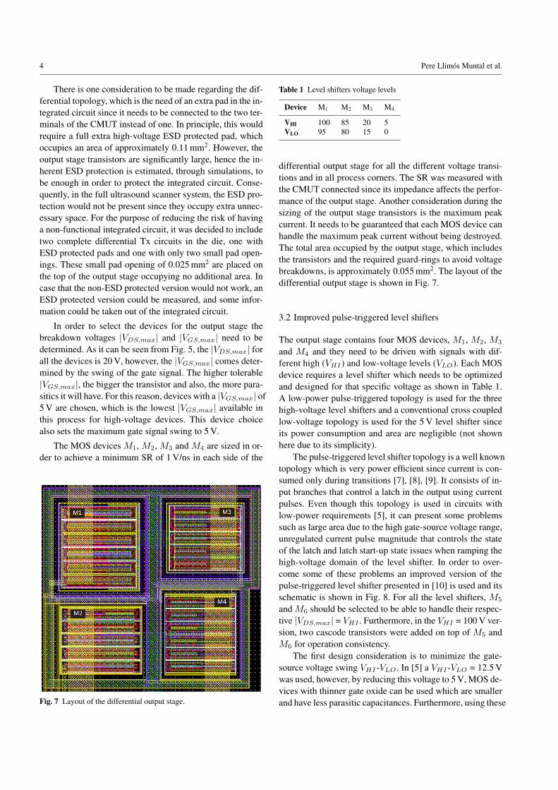
3.2 Improved pulse-triggered level shifters
The output stage contains four MOS devices, M1, M2, M3
and M4 and they need to be driven with signals with dif-ferent high (VHI ) and low-voltage levels (VLO). Each MOSdevice requires a level shifter which needs to be optimizedand designed for that specific voltage as shown in Table 1.A low-power pulse-triggered topology is used for the threehigh-voltage level shifters and a conventional cross coupledlow-voltage topology is used for the 5 V level shifter sinceits power consumption and area are negligible (not shownhere due to its simplicity).
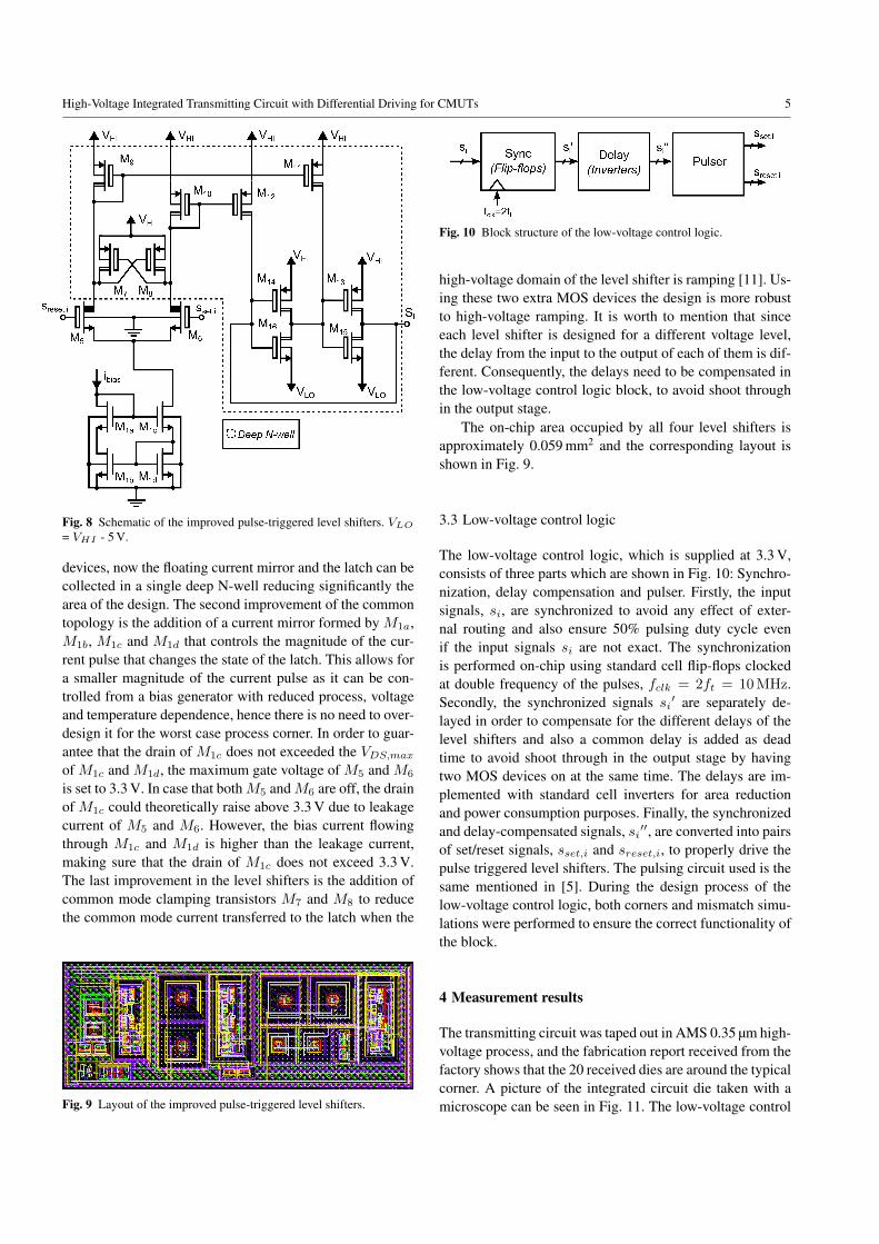
The pulse-triggered level shifter topology is a well knowntopology which is very power efficient since current is con-sumed only during transitions [7], [8], [9]. It consists of in-put branches that control a latch in the output using currentpulses. Even though this topology is used in circuits withlow-power requirements [5], it can present some problemssuch as large area due to the high gate-source voltage range,unregulated current pulse magnitude that controls the stateof the latch and latch start-up state issues when ramping thehigh-voltage domain of the level shifter. In order to over-come some of these problems an improved version of thepulse-triggered level shifter presented in [10] is used and itsschematic is shown in Fig. 8. For all the level shifters, M5
and M6 should be selected to be able to handle their respec-tive |VDS,max| = VHI . Furthermore, in the VHI = 100 V ver-sion, two cascode transistors were added on top of M5 andM6 for operation consistency.
The first design consideration is to minimize the gate-source voltage swing VHI -VLO. In [5] a VHI -VLO = 12.5 Vwas used, however, by reducing this voltage to 5 V, MOS de-vices with thinner gate oxide can be used which are smallerand have less parasitic capacitances. Furthermore, using these
High-Voltage Integrated Transmitting Circuit with Differential Driving for CMUTs 5
Fig. 8 Schematic of the improved pulse-triggered level shifters. VLO
= VHI - 5 V.
devices, now the floating current mirror and the latch can becollected in a single deep N-well reducing significantly thearea of the design. The second improvement of the commontopology is the addition of a current mirror formed by M1a,M1b, M1c and M1d that controls the magnitude of the cur-rent pulse that changes the state of the latch. This allows fora smaller magnitude of the current pulse as it can be con-trolled from a bias generator with reduced process, voltageand temperature dependence, hence there is no need to over-design it for the worst case process corner. In order to guar-antee that the drain of M1c does not exceeded the VDS,max
of M1c and M1d, the maximum gate voltage of M5 and M6
is set to 3.3 V. In case that bothM5 andM6 are off, the drainof M1c could theoretically raise above 3.3 V due to leakagecurrent of M5 and M6. However, the bias current flowingthrough M1c and M1d is higher than the leakage current,making sure that the drain of M1c does not exceed 3.3 V.The last improvement in the level shifters is the addition ofcommon mode clamping transistors M7 and M8 to reducethe common mode current transferred to the latch when the
Fig. 9 Layout of the improved pulse-triggered level shifters.
Fig. 10 Block structure of the low-voltage control logic.
high-voltage domain of the level shifter is ramping [11]. Us-ing these two extra MOS devices the design is more robustto high-voltage ramping. It is worth to mention that sinceeach level shifter is designed for a different voltage level,the delay from the input to the output of each of them is dif-ferent. Consequently, the delays need to be compensated inthe low-voltage control logic block, to avoid shoot throughin the output stage.
The on-chip area occupied by all four level shifters isapproximately 0.059 mm2 and the corresponding layout isshown in Fig. 9.
3.3 Low-voltage control logic
The low-voltage control logic, which is supplied at 3.3 V,consists of three parts which are shown in Fig. 10: Synchro-nization, delay compensation and pulser. Firstly, the inputsignals, si, are synchronized to avoid any effect of exter-nal routing and also ensure 50% pulsing duty cycle evenif the input signals si are not exact. The synchronizationis performed on-chip using standard cell flip-flops clockedat double frequency of the pulses, fclk = 2ft = 10MHz.Secondly, the synchronized signals si′ are separately de-layed in order to compensate for the different delays of thelevel shifters and also a common delay is added as deadtime to avoid shoot through in the output stage by havingtwo MOS devices on at the same time. The delays are im-plemented with standard cell inverters for area reductionand power consumption purposes. Finally, the synchronizedand delay-compensated signals, si′′, are converted into pairsof set/reset signals, sset,i and sreset,i, to properly drive thepulse triggered level shifters. The pulsing circuit used is thesame mentioned in [5]. During the design process of thelow-voltage control logic, both corners and mismatch simu-lations were performed to ensure the correct functionality ofthe block.
4 Measurement results
The transmitting circuit was taped out in AMS 0.35 µm high-voltage process, and the fabrication report received from thefactory shows that the 20 received dies are around the typicalcorner. A picture of the integrated circuit die taken with amicroscope can be seen in Fig. 11. The low-voltage control

6 Pere Llimos Muntal et al.
logic is located in area a) with an area of 0.01 µm2, the levelshifters are situated in area b) with an area of 0.059 mm2 andthe differential output stage is located in c) and occupies anarea of 0.055 mm2. The total area of the transmitting circuitaccounting also for the routing is 0.18 mm2.
As previously mentioned, two full transmitting circuitswere included in the die, one with ESD protected pads and asecond one with just pad openings. Some initial ESD evalua-tion tests were performed on the non ESD protected versionobtaining very robust results and consistent performance,even through reckless integrated circuit manipulation. Con-sequently, all measurement results were made with the non-ESD protected Tx, since the ESD protection would not bepart of the ultrasound scanner system. The complete ESDevaluation is going to be performed in the future.
For the purpose of assessing the performance of the trans-mitting circuit, a PCB was built to test it. The measure-ment setup used is shown in Fig. 12. Two Hewlett PackardE3612A voltage supplies were used to generate 20 V and100 V, and from those voltages the on-board linear regula-tors generate the rest of the voltage levels used in the Tx,5 V, 15 V, 80 V, 85 V and 95 V. During the current mea-surements, only the current from each voltage level fed intothe chip was accounted, hence the current sunk by the linearregulators was not considered. The low-voltage input signalsand the low-voltage supply were generated using an exter-nal Xilinx Spartan-6 LX45 FPGA with a maximum clockfrequency of 80 MHz and 3.3 V operation. The voltage out-puts of the Tx connected to the transducer and the currentconsumption were measured using a Tektronix MSO4104Boscilloscope and a Tektronix TCP202 current probe.
Using the described setup, the integrated circuit was tes-ted with pulses from 60 V to 100 V, frequency of 5 MHz, areceiving bias voltage of 80 V and ultrasound scanner trans-mitting duty cycle of 1/266. The measured voltage of thetwo terminals of the CMUT and the differential voltage be-
Fig. 11 Picture of the taped-out differential transmitting circuit. a) a’)Low-voltage logic, b) b’) Level shifters, c) c’) Output stage.
Fig. 12 Setup for the integrated circuit measurements.
tween the plates of the CMUT can be seen in Fig. 13. Thebias voltage is stable at 80 V when receiving and it togglesaccording to the input signals supplied between 60 V and100 V at a measured frequency of 5 MHz when transmitting.
The transmitting circuit power consumption is charac-terized with no load, with the equivalent capacitance of theCMUT connected and with the full electrical model of theCMUT connected. In order to measure the power consump-tion of the Tx for these three load scenarios, the currentsfrom all the voltage sources supplying the integrated circuitwere measured for each case. The measurements are shownin Table 2. The currents measured from the 5 V, 15 V, 85 Vand 95 V supplies were negligible compared to the ones mea-sured in the other voltage supplies, so they are accounted aszero and are not shown in the table. Using these current mea-surements, the power consumption can be calculated obtain-ing 0.056 mW for the non-loaded Tx, 0.754 mW for the Txwith the equivalent capacitance of the CMUT connected and0.936 mW for the Tx with the electrical model of the CMUTconnected. These numbers highly correlate with the resultsof the simulations with parasitics of 0.052 mW, 0.712 mWand 0.894 mW respectively.
Fig. 13 Measurements of the output terminals of the differential trans-mitting circuit. The red trace and green trace are the voltages measuredat the high-voltage and low-voltage terminals of the Tx respectively.The cyan trace is the differential voltage between them.

High-Voltage Integrated Transmitting Circuit with Differential Driving for CMUTs 7
The minimum SR measured in the high-voltage termi-nal of the Tx is SRH = 0.91 V/ns and the SR measured inthe low-voltage terminal is SRL = 1.12 V/ns. The result-ing differential SR seen from the CMUT load is 2.03 V/ns.These results are a bit below the simulated values with par-asitics, which for the typical corner were SRH = 1.09 V/nsand SRL = 1.23 V/ns. This slightly reduced slew rate is at-tributed to the external PCB routing and the capacitance ofthe probes used to measure, which affect the total load ca-pacitance that the Tx has to charge and discharge. For thepurpose of comparing the simulation results and measure-ments accurately, the equivalent capacitances of the probeswere added to the simulation testbench of the Tx in the typ-ical corner and extracted parasitics. SRH and SRL weresimulated again obtaining 0.97 V/ns and 1.17 V/ns respec-tively, which are now much closer to the measured results.This simulation can be performed again through the cornersleading to SRH = 0.76 V/ns and SRL = 0.94 V/ns for theslowest corner and SRH = 1.15 V/ns and SRL = 1.40 V/nsfor the fastest corner. According to these numbers, the diesreceived seem to be very close to typical corner as it wasreported from the factory.
Even though the received dies are around the typical cor-ner, the local process variations generate a spread on theperformance of each die. In order to assess this variationon fabricated dies, the minimum SRH and SRL of the 20fabricated integrated circuits were measured and comparedto the expected variation from the simulations. In Fig. 14the histograms of SRH and SRL obtained from a MonteCarlo simulation are shown. The simulation was made withextracted parasitics, in the typical corner, and using 100 ran-
a) SRH
[V/ns]0.7 0.8 0.9 1 1.1 1.2 1.30
5
10
15
20
25SimulationMeasurements
b) SRL [V/ns]
0.7 0.8 0.9 1 1.1 1.2 1.30
5
10
15
20
25SimulationMeasurements
Fig. 14 Monte carlo simulation with 100 random points in the typicalcorner and extracted parasitics plotted in blue. Measurement results ofthe 20 dies in red.
dom points. The equivalent capacitances of the measuringprobes were also included in the simulation. The measuredresults from the 20 dies, which are also close to the typi-cal corner, are plotted on top of the simulated distribution.Even though the measured sample size is not big enough totake direct conclusions, it can be seen that for both SRH andSRL the samples fall around the expected values. Howeverit is still unclear how the simulated and measured distribu-tions differ.
Typically, when analyzing samples, it is common to showthe ±3σ limits without taking into account the number ofsamples used and directly compare them with the expecteddistribution. This approach is highly problematic due to sev-eral false assumptions as it is suggested in [12]. In orderto show this information more precisely, the approach sug-gested in [12] is used resulting in Fig. 15. The SRH andSRL of the 20 measured samples (N = 20) and their re-spective median range M and percentiles P15.87 and P84.13
for a confidence level of 95% are shown. For the purpose ofcomparing the measured results with the simulation results,the same information is plotted for the 100 Monte Carlo it-erations. As it can be seen, there is a good correlation be-tween results. However, the measured M ranges are 6% to10% lower than the simulated ones, which is very likely dueto external PCB routing and fabrication not being exactlyin the typical corner. Furthermore, the measured M rangesare wider due to the lower number of samples compared tothe simulations. The percentiles are similarly spread aroundM for the SRH , but for the SRL, the P84.13 percentile ismuch narrower. These results could be caused by variancedue to small sample size. Overall, there is a high correlationbetween the expected results from simulations and measure-ments.
a) SRH
[V/ns]0.8 0.85 0.9 0.95 1 1.05 1.1 1.15 1.2 1.25 1.3 1.35 1.4
MP15.87
P84.13
MP15.87
P84.13
b) SRL [V/ns]
0.8 0.85 0.9 0.95 1 1.05 1.1 1.15 1.2 1.25 1.3 1.35 1.4
MP15.87
P84.13
MP15.87
P84.13
MeasurementsSimulation
Fig. 15 Data sets of SRH and SRL for a 95% confidence level, show-ing the spread of the medianM and the percentiles P15.87 and P84.13
for N = 20.

8 Pere Llimos Muntal et al.
Table 2 Current measurements on the integrated circuit
Vsupply [V] 100 80 20
Ino-load [µA] 1.65 -1.69 1.29Icapacitive-load [µA] 14.3 -12.2 15.0ICMUT-load [µA] 30.6 -34.9 33.4
Table 3 Transmitting circuit performance comparison
[5] this work %
On-chip area [mm2] 0.938 0.18 -80.8Pno-load [mW] - 0.056 -Pcapacitive-load [mW] 1.8 0.754 -58.2PCMUT-load [mW] - 0.936 -
5 Discussion
The design presented can not be compared directly withstate of the art transmitting circuits since the references foundeither do not specify the driving conditions, area and powerconsumption or only the full channel consumption, includ-ing the receiving circuitry, is stated [13], [14], [15]. Never-theless, a comparison with the single-ended driving topol-ogy in [5] can performed since both area and power con-sumption with a capacitive load are stated. The operatingconditions in [5] are different: The pulse voltage swing is50 V, the duty cycle is 50% and a load is 15 pF. In orderto compare the topologies accurately, the same operatingconditions should be defined. The conditions chosen are theones closest to the operation of an ultrasound scanner suchas the ones defined in this paper: pulse voltage range of 40 V,pulsing frequency of 5 MHz, a transmitting duty cycle of1/266 and an capacitive load of 30 pF, which is the equiv-alent capacitance of the CMUT. Adjusting the power con-sumption of [5] to the operation conditions of an ultrasoundscanner, a comparison can be performed and a summary isshown in Table 3. The differential Tx presented in this paperachieves a very significant area reduction of 80.8% and thepower consumption is reduced by 58.2%.
The measurements performed show a good correlationwith the simulated results, which increases the reliability ofthe simulations. Even though the measured sample size islimited to the amount of dies received, the design shows tobe solid and functional through local process variations. Itcan probably be expected that the Tx will behave accordingto the simulations in other process corners, however, in or-der to prove that, the design should be fabricated with thespecific corner conditions desired to test. Nevertheless, dueto the good correlation between simulations and measure-ments, any future tapeout with an improved Tx has a lowerrisk to generate a non-functional integrated circuit.
The next step for the Tx would be to implement on-chipvoltage regulation. As mentioned before, the number of volt-
age levels required in the Tx is significantly high and a lotof external extra circuitry is required to generate them. Onlyone high-voltage supply would be needed with internal volt-age regulation, furthermore, the high-voltage ramping of allthe level shifters would be better controlled.
6 Conclusions
In this paper a differential integrated high-voltage transmit-ting circuit for CMUTs is successfully designed and imple-mented in AMS 0.35 µm high-voltage process. The circuitsupplies pulses with a frequency of 5 MHz, voltage levels of60 V, 80 V and 100 V and a measured slew rate of 2.03 V/nswith the load connected. The transmitting circuit is mea-sured under the operation conditions of an ultrasound scan-ner in order to accurately assess the performance of the cir-cuitry. The total operating power consumption measured onthe integrated circuit is 0.936 mW and the circuit occupiesan on-chip area of 0.18 mm2 obtaining a small and efficientthe transmitting circuit very suitable for portable ultrasoundscanner applications. The design shows to be robust throughlocal process variations and a high correlation between mea-surements and simulations is found.
References
1. Arif. S.Ergun, Goksen G. Yaralioglu and Butrus T. Khuri-Yakub,”Capacitive Micromachined Ultrasonic Transducers: Theory andTechnology” in Journal of Aerospace Engineering, pp.74-87, 2003.
2. G. Gurun, P. Hasler and F.L. Degertekin, ”Front-End Receiver Elec-tronics for High- Frequency Monolithic CMUT-on-CMOS ImagingArrays” in IEEE Transactions on Ultrasonics, Ferroelectrics, andFrequency Control, Vol. 58, No. 8, pp.1658-1668, 2011.
3. Butrus T. Khuri-Yakub and Omer Oralkan, ”Capacitive microma-chined ultrasonic transducers for medical imaging and therapy” inJournal of Micromechanics and Microengineering, Vol. 21, pp.1-11, 2011.
4. P. Llimos Muntal, D. Ø. Larsen, K. Færch, I. H.H. Jørgensen andE. Bruun, ”Integrated Differential High-Voltage Transmitting Cir-cuit for CMUTs” in IEEE 13th International New Circuits and Sys-tems Conference (NEWCAS), 2015.
5. P. Llimos Muntal, D. Ø. Larsen, I. H.H. Jørgensen and E. Bruun,”Integrated reconfigurable high-voltage transmitting circuit forCMUTs” in Analog Integrated Circuits and Signal Processing, Vol.84, Issue 3, pp.343-352, 2015.
6. K. Chen, H-S. Lee, A.P. Chandrakasan and C.G. Sodini, ”Ultra-sonic Imaging Transceiver Design for CMUT: A Three-Level 30-Vpp Pulse-Shaping Pulser With Improved Efficiency and a Noise-Optimized Receiver” in IEEE Journal of Solid-State Circuits, Vol.48, No. 11, pp.2734-2745, 2013.
7. H. Ma, R. van der Zee, and B. Nauta, ”Design and Analysis ofa High-Efficiency High-Voltage Class-D Power Output Stage” inIEEE Journal of Solid-State Circuits, Vol. 49, No. 7, pp.1514-1524,2014.
8. T. Lehmann, ”Design of fast low-power floating high-voltage level-shifters.” in Electronics Letters, Vol. 50, No. 3, p. 1, 2014.
9. D. Liu, S. J. Hollis, and B. H. Stark, ”A new circuit topology forfloating high voltage level shifters” in 10th Conference on Ph.D.
High-Voltage Integrated Transmitting Circuit with Differential Driving for CMUTs 9
Research in Microelectronics and Electronics (PRIME), pp. 1-4,2014.
10. D. Ø. Larsen, P. Llimos Muntal, I. H.H. Jørgensen and E. Bruun,”High-voltage Pulse-triggered SR Latch Level-Shifter Design Con-siderations” in 32nd Norchip Conference, 2014.
11. H. Ma, R. van der Zee, and B. Nauta, ”Design and Analysis ofa High-Efficiency High-Voltage Class-D Power Output Stage” inSolid-State Circuits, IEEE Journal of, vol.49, no.7, pp.1514-1524,2014.
12. H.Schmid and A. Huber, ”Measuring a Small Number of Samples,and the 3σ Fallacy: Shedding Light on Confidence and Error Inter-vals” in Solid-State Circuits Magazine, IEEE, vol.6, no.2, pp.52-58,2014.
13. I.O. Wygant, X. Zhuang, D.T. Yeh, . Oralkan, A.S. Ergun,M. Karaman and B.T. Khuri-Yakub, ”Integration of 2D CMUT Ar-rays with Front-End Electronics for Volumetric Ultrasound Imag-ing” in IEEE Transactions on Ultrasonics, Ferroelectrics, and Fre-quency Control, Vol. 55, No. 2, pp.327-342, 2008.
14. G. Gurun, P. Hasler and F.L. Degertekin, ”A 1.5-mm DiameterSingle-Chip CMOS Front-End System with Transmit-Receive Ca-pability for CMUT on-CMOS Forward-Looking IVUS” in IEEEInternational Ultrasonics Symposium Proceedings, pp.478-481,2011.
15. Sung-J. Jung, Jong-K. Song and Oh-K. Kwon, ”Three-Side But-table Integrated Ultrasound Chip With a 16 16 ReconfigurableTransceiver and Capacitive Micromachined Ultrasonic TransducerArray for 3-D Ultrasound Imaging Systems” in IEEE Transactionson Electron Devices, Vol. 60, No. 10, pp.3562-3569, 2013.