Embed Size (px)
Citation preview

High-Voltage Impulse GeneratorHigh-Voltage Impulse Generator
ECE–490 Senior Design Project Dr. Ken KaiserSummer 2002
Domenic DeGiuliJohn Murlick
Cindy Nguyen-DangAkhil Nutakki

Project GoalProject Goal
The project was intended to challenge students to meet the The project was intended to challenge students to meet the following formal program educational objectives defined by following formal program educational objectives defined by the electrical engineering faculty:the electrical engineering faculty:
Ability to analyze and design basic electrical, electronic and Ability to analyze and design basic electrical, electronic and digital systems.digital systems.
Necessary interpersonal and communications skills to be Necessary interpersonal and communications skills to be productive members in a team work environment.productive members in a team work environment.
Development of experience and self-confidence to be Development of experience and self-confidence to be technical and/or managerial leaders.technical and/or managerial leaders.
Consciousness of safety, ethical and professional Consciousness of safety, ethical and professional responsibilities of an engineer.responsibilities of an engineer.

Project Requirements/SpecificationsProject Requirements/Specifications Battery - 3V Duracell CR2032 220 ma-HrBattery - 3V Duracell CR2032 220 ma-Hr Load - voltage divider network setup with a 500Load - voltage divider network setup with a 500ΩΩ and a 20 and a 20ΩΩ high power high power
resistorresistor Volume - 100 cmVolume - 100 cm33
Charge up Time - one minute max. with an indicator (“ready”) lightCharge up Time - one minute max. with an indicator (“ready”) light Printed Circuit Board - must be carefully designed and professionally Printed Circuit Board - must be carefully designed and professionally
finished with no gluing, no surface mounted devices (SMD), and with finished with no gluing, no surface mounted devices (SMD), and with sockets for all transistors and integrated circuitssockets for all transistors and integrated circuits
Professional connectors between major componentsProfessional connectors between major components Stranded wire between componentsStranded wire between components Chassis - quick access to the battery and switchesChassis - quick access to the battery and switches No screws through or into plasticNo screws through or into plastic Indication of when impulse generator is readyIndication of when impulse generator is ready Neat LabelingNeat Labeling No Mechanical GeneratorsNo Mechanical Generators Two probes – connected to High Voltage Impulse; must not have long wiresTwo probes – connected to High Voltage Impulse; must not have long wires
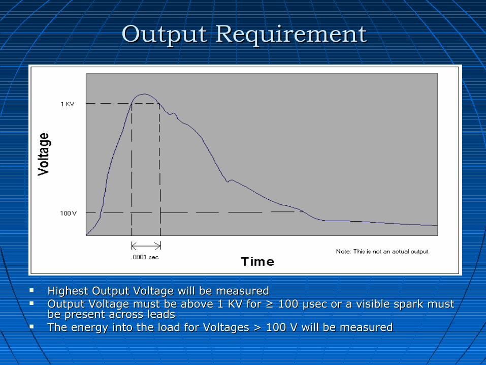
Output RequirementOutput Requirement
Highest Output Voltage will be measuredHighest Output Voltage will be measured Output Voltage must be above 1 KV for ≥ 100 Output Voltage must be above 1 KV for ≥ 100 μμsec or a visible spark must sec or a visible spark must
be present across leadsbe present across leads The energy into the load for Voltages > 100 V will be measured The energy into the load for Voltages > 100 V will be measured

Bonus Points awarded to Groups in Bonus Points awarded to Groups in Various Categories Various Categories
Smallest SizeSmallest Size Highest Output Voltage Highest Output Voltage Highest Energy into load Highest Energy into load
(for > 100 V)(for > 100 V) Appearance (outside) Appearance (outside) Ease of useEase of use

Engineering NotebooksEngineering Notebooks
An unique engineering notebook is kept by each An unique engineering notebook is kept by each individual studentindividual student
The notebook is signed and dated on each pageThe notebook is signed and dated on each page It contains all the work performed by the student It contains all the work performed by the student
for the design project (sketches, contacts, for the design project (sketches, contacts, schematics, ideas etc.) schematics, ideas etc.)

Project MilestonesProject Milestones
Milestone 1Milestone 1(100pts)(100pts)
Paper design Paper design w/some PSpicew/some PSpice
OscillatorOscillator Battery Battery
characteristics characteristics experiments; experiments;
(V(Vococ, R, Rthth, I, Imaxmax, E, Etottot))
Milestone 3Milestone 3(141 pts)(141 pts)
PCB Board PCB Board versionversion
Components Components need not be need not be connectedconnected
Chassis to show Chassis to show all buttons and all buttons and switchesswitches
Probes Probes
Milestone 2Milestone 2(150 pts)(150 pts)
Battery operated Battery operated working working prototypeprototype
Load-Test setupLoad-Test setup
The project is spilt up into three milestones for organization and to The project is spilt up into three milestones for organization and to ensure that it will be completed on timeensure that it will be completed on time

How does a High Voltage How does a High Voltage Impulse Generator Work?Impulse Generator Work?
The circuit starts with a 3 VoltThe circuit starts with a 3 Volt battery battery; It supplies electricity to a circuit ; It supplies electricity to a circuit consisting of various electrical components.consisting of various electrical components.
After the battery is an After the battery is an oscillatoroscillator; It fluctuates current to produce a ; It fluctuates current to produce a specific pulse pattern of electricity.specific pulse pattern of electricity.
After the oscillator is a After the oscillator is a transformertransformer; It boosts the voltage in the circuit, ; It boosts the voltage in the circuit, and reduces the amperage.and reduces the amperage.
After the transformer is a After the transformer is a multiplier circuitmultiplier circuit; It further increases the ; It further increases the overall voltage.overall voltage.
After the multiplier circuit is a After the multiplier circuit is a capacitorcapacitor; It builds up a charge, and ; It builds up a charge, and releases it to the probes.releases it to the probes.
After the capacitor are the After the capacitor are the probesprobes (electrodes); They are simply two (electrodes); They are simply two plates of conducting metal positioned in the circuit with a gap between plates of conducting metal positioned in the circuit with a gap between them. Since the probes are positioned along the circuit, they have a high them. Since the probes are positioned along the circuit, they have a high voltage difference between them. voltage difference between them.
When the gap is filled with a When the gap is filled with a conductorconductor (a person perhaps?), the electrical (a person perhaps?), the electrical pulses will try to move from one electrode the other, dumping electricity pulses will try to move from one electrode the other, dumping electricity through the conductor.through the conductor.
There is a There is a buttonbutton that is pressed to start the charge cycle. that is pressed to start the charge cycle. There is a There is a neon lamp indicatorneon lamp indicator which lights when the circuit is capable of which lights when the circuit is capable of
producing the appropriate voltage (≥ 1000 volts).producing the appropriate voltage (≥ 1000 volts).
*A circuit schematic can be seen on the next slide*A circuit schematic can be seen on the next slide

SchematicSchematic

Technical DataTechnical Data
Charge-up CircuitCharge-up Circuit Multiplier CircuitMultiplier Circuit Output CircuitOutput Circuit
For a better understanding we need to take an in-depth look For a better understanding we need to take an in-depth look at the functionality and design of a high voltage impulse at the functionality and design of a high voltage impulse generator. We can discuss it in terms of three main stages generator. We can discuss it in terms of three main stages and the integration of those stages:and the integration of those stages:

Charge-Up CircuitCharge-Up CircuitThe main components of the charge up The main components of the charge up circuit consist of a 555 timer, a bipolar circuit consist of a 555 timer, a bipolar junction transistor (BJT), and a junction transistor (BJT), and a transformer. The output of the 555 transformer. The output of the 555 timer operates as an oscillator timer operates as an oscillator producing a 20 kHz, 3 V, peak to peak producing a 20 kHz, 3 V, peak to peak square wave. The signal from the 555 square wave. The signal from the 555 timer is used to drive the base of the timer is used to drive the base of the BJT, thus turning it on and off. The BJT BJT, thus turning it on and off. The BJT is used to drive the voltage step up is used to drive the voltage step up transformer via connection between the transformer via connection between the primary side of the transformer and to primary side of the transformer and to ground. The high voltage induced in the ground. The high voltage induced in the secondary of the transformer is secondary of the transformer is determined by the 6:1750 turns ratio to determined by the 6:1750 turns ratio to the primary windings. Thus, the battery the primary windings. Thus, the battery voltage supplied is correspondingly voltage supplied is correspondingly stepped up by the transformer to stepped up by the transformer to approximately 600 VAC on the approximately 600 VAC on the secondary side. secondary side.
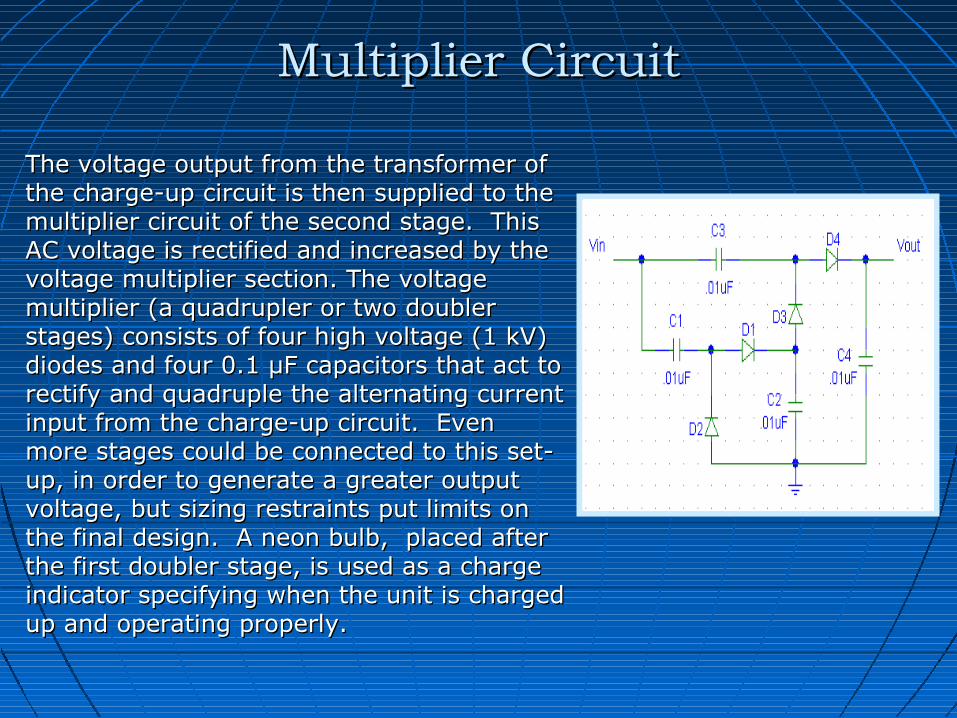
Multiplier CircuitMultiplier Circuit
The voltage output from the transformer of The voltage output from the transformer of the charge-up circuit is then supplied to the the charge-up circuit is then supplied to the multiplier circuit of the second stage. This multiplier circuit of the second stage. This AC voltage is rectified and increased by the AC voltage is rectified and increased by the voltage multiplier section. The voltage voltage multiplier section. The voltage multiplier (a quadrupler or two doubler multiplier (a quadrupler or two doubler stages) consists of four high voltage (1 kV) stages) consists of four high voltage (1 kV) diodes and four 0.1 μF capacitors that act to diodes and four 0.1 μF capacitors that act to rectify and quadruple the alternating current rectify and quadruple the alternating current input from the charge-up circuit. Even input from the charge-up circuit. Even more stages could be connected to this set-more stages could be connected to this set-up, in order to generate a greater output up, in order to generate a greater output voltage, but sizing restraints put limits on voltage, but sizing restraints put limits on the final design. A neon bulb, placed after the final design. A neon bulb, placed after the first doubler stage, is used as a charge the first doubler stage, is used as a charge indicator specifying when the unit is charged indicator specifying when the unit is charged up and operating properly. up and operating properly.

Output CircuitOutput Circuit
The voltage at the output of the The voltage at the output of the multiplier stage is then used to charge a multiplier stage is then used to charge a capacitor bank before a switch is capacitor bank before a switch is triggered to release the voltage, which triggered to release the voltage, which terminates at the electrodes. These terminates at the electrodes. These electrodes have been integrated into the electrodes have been integrated into the PCB, separated by 1 cm in order to PCB, separated by 1 cm in order to avoid sparking. The current will only avoid sparking. The current will only travel across these electrodes if an travel across these electrodes if an outside conductor is inserted betweenoutside conductor is inserted betweenthe electrodes. A mechanical sparking switch was integrated into the the electrodes. A mechanical sparking switch was integrated into the chassis consisting simply of a metal strip that when depressed by a chassis consisting simply of a metal strip that when depressed by a button, creates a smaller gap between the two discharge electrodes. button, creates a smaller gap between the two discharge electrodes. The resulting voltage output of this circuit is high enough to ionize the The resulting voltage output of this circuit is high enough to ionize the air particles between the metal strip and the discharge electrodes; air particles between the metal strip and the discharge electrodes; thus, the flow of charge continues until the capacitor bank is thus, the flow of charge continues until the capacitor bank is discharged displaying a visible spark and crackling noise. discharged displaying a visible spark and crackling noise.

Integration of Three Circuit StagesIntegration of Three Circuit StagesAltogether, there are three switches that permit a fully functional circuit. The first Altogether, there are three switches that permit a fully functional circuit. The first ((powerpower) switch connects the battery to the charge-up circuit. When depressed, a ) switch connects the battery to the charge-up circuit. When depressed, a button (button (chargecharge) switch within the charge-up circuit provides the necessary ) switch within the charge-up circuit provides the necessary current path, allowing the transformer to step up the voltage, which is then current path, allowing the transformer to step up the voltage, which is then multiplied. A neon indicator light located within the first doubler stage is activated multiplied. A neon indicator light located within the first doubler stage is activated at approximately 300 V. When the neon light goes on, signaling that the at approximately 300 V. When the neon light goes on, signaling that the capacitors have charged up to a suitable voltage level, the last button (capacitors have charged up to a suitable voltage level, the last button (firefire) switch ) switch is then depressed allowing the capacitors at the output stage to discharge. This is then depressed allowing the capacitors at the output stage to discharge. This step releases the voltage stored within the capacitor network to the discharge step releases the voltage stored within the capacitor network to the discharge electrodes.electrodes.
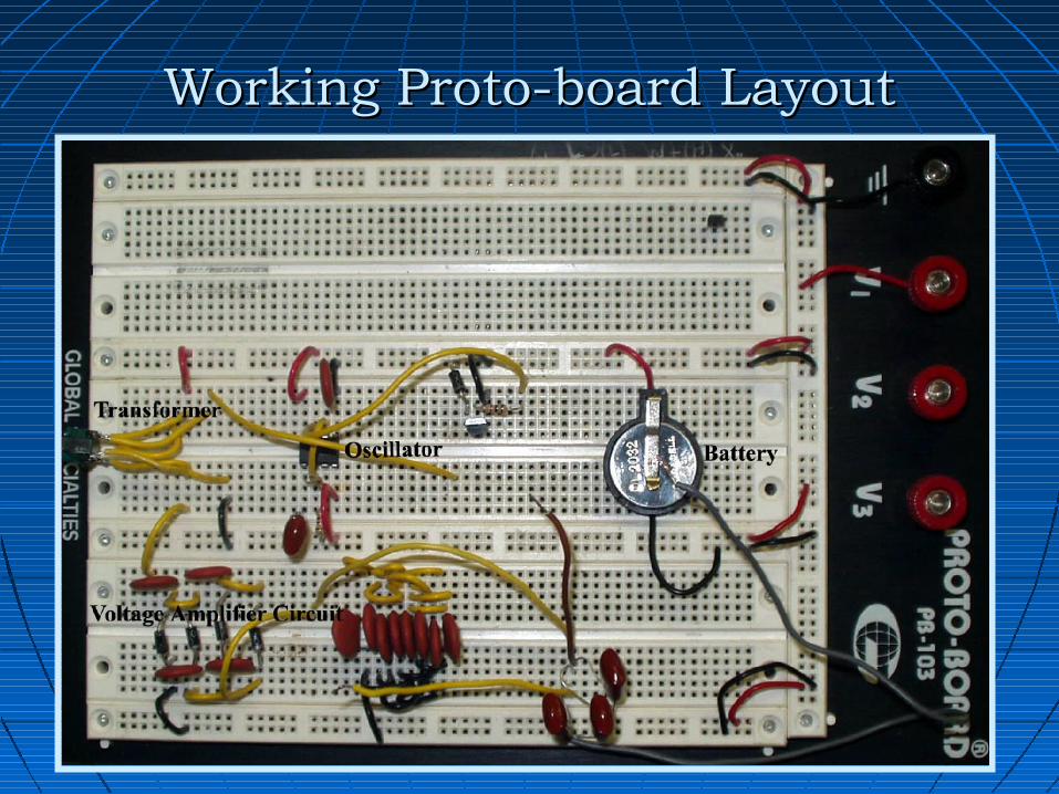
Working Proto-board LayoutWorking Proto-board Layout

PCB Board VersionPCB Board Version
<- Printed Circuit Board <- Printed Circuit Board without components without components attachedattached
Complete circuit board (bothComplete circuit board (bothsides), with all componentssides), with all componentsattached; including the probesattached; including the probesand light indicatorand light indicator
<-<-
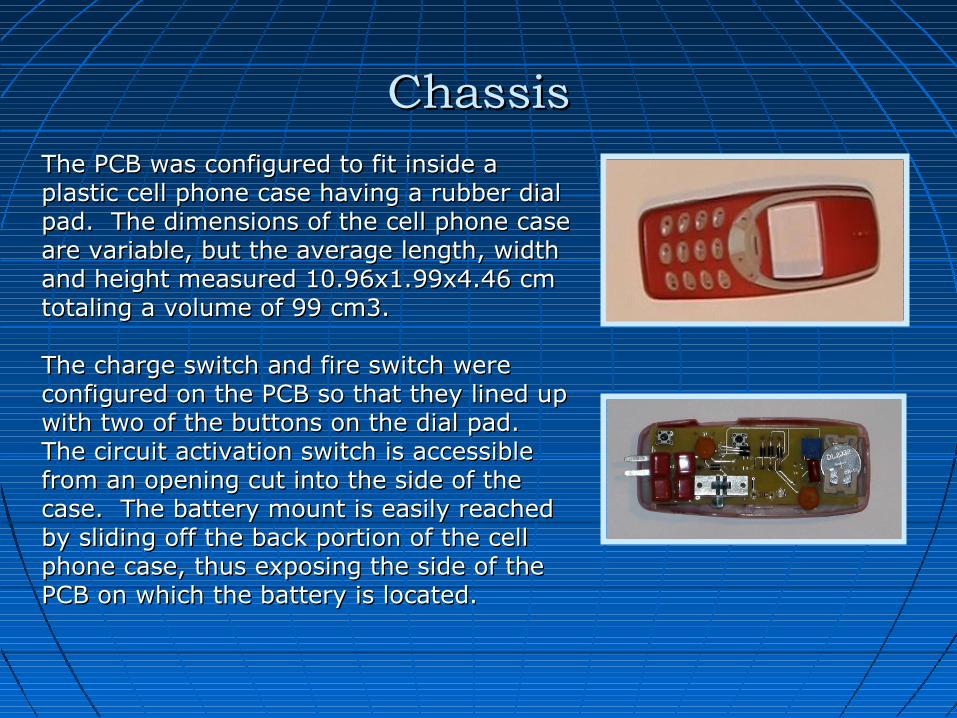
ChassisChassisThe PCB was configured to fit inside a The PCB was configured to fit inside a plastic cell phone case having a rubber dial plastic cell phone case having a rubber dial pad. The dimensions of the cell phone case pad. The dimensions of the cell phone case are variable, but the average length, width are variable, but the average length, width and height measured 10.96x1.99x4.46 cm and height measured 10.96x1.99x4.46 cm totaling a volume of 99 cm3. totaling a volume of 99 cm3.
The charge switch and fire switch were The charge switch and fire switch were configured on the PCB so that they lined up configured on the PCB so that they lined up with two of the buttons on the dial pad. with two of the buttons on the dial pad. The circuit activation switch is accessible The circuit activation switch is accessible from an opening cut into the side of the from an opening cut into the side of the case. The battery mount is easily reached case. The battery mount is easily reached by sliding off the back portion of the cell by sliding off the back portion of the cell phone case, thus exposing the side of the phone case, thus exposing the side of the PCB on which the battery is located.PCB on which the battery is located.

Experimental Set-up/ResultsExperimental Set-up/Results
The load set-up was configured as The load set-up was configured as illustrated on the right.illustrated on the right.
The oscilloscope was set up to read 10 The oscilloscope was set up to read 10 V per division along the y-axis with a V per division along the y-axis with a 50 μs time base.50 μs time base.
The charge switch was depressed until The charge switch was depressed until the indicator light illuminated.the indicator light illuminated.
The fire switch was then pressed and The fire switch was then pressed and the resulting output was viewed on the the resulting output was viewed on the oscilloscope.oscilloscope.
Since the output voltage of the circuit is much higher than the voltage Since the output voltage of the circuit is much higher than the voltage capabilities of the oscilloscope, it was necessary to step down the capabilities of the oscilloscope, it was necessary to step down the voltage. A voltage divider was configured using high voltage, high voltage. A voltage divider was configured using high voltage, high power, inductive resistors, which are approximately equal to 500 power, inductive resistors, which are approximately equal to 500 ΩΩ (Ohmite model 47824) and 20 (Ohmite model 47824) and 20 ΩΩ (Biddle model 41 1K85C5). This (Biddle model 41 1K85C5). This resistor set-up provided a voltage ratio of 26:1.resistor set-up provided a voltage ratio of 26:1.
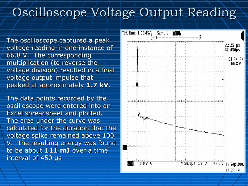
Oscilloscope Voltage Output ReadingOscilloscope Voltage Output Reading
The oscilloscope captured a peak The oscilloscope captured a peak voltage reading in one instance of voltage reading in one instance of 66.8 V. The corresponding 66.8 V. The corresponding multiplication (to reverse the multiplication (to reverse the voltage division) resulted in a final voltage division) resulted in a final voltage output impulse that voltage output impulse that peaked at approximately peaked at approximately 1.7 kV1.7 kV..
The data points recorded by the The data points recorded by the oscilloscope were entered into an oscilloscope were entered into an Excel spreadsheet and plotted. Excel spreadsheet and plotted. The area under the curve was The area under the curve was calculated for the duration that the calculated for the duration that the voltage spike remained above 100 voltage spike remained above 100 V. The resulting energy was found V. The resulting energy was found to be about to be about 111 mJ111 mJ over a time over a time interval of 450 μsinterval of 450 μs

Final Product Final Product

BONUS AWARDS!!BONUS AWARDS!!
Smallest Size: Winner (Smallest Size: Winner (33), 8.7*10), 8.7*1044 mm mm33 Highest Output Voltage: Winner (Highest Output Voltage: Winner (33), ~19872 V), ~19872 VHighest Energy into load: Winner (Highest Energy into load: Winner (44))Appearance: Winner (Appearance: Winner (44) ) Ease of use: Winner (Ease of use: Winner (66))

Conclusion
The High Voltage Impulse Generator The High Voltage Impulse Generator design project intended to challenge design project intended to challenge students and met many of the formal students and met many of the formal program educational objectives program educational objectives defined by the electrical engineering defined by the electrical engineering faculty. It provided students with a faculty. It provided students with a fun, educational experience which will fun, educational experience which will help provide a solid foundation for help provide a solid foundation for future engineering work.future engineering work.

![Code No: HIGH VOLTAGE ENGINEERING - padhle.com · impulse generator circuits. [7] 5 a) ... Explain about tripping and control of impulse generators. [7] 5 a) With neat sketch,](https://img.dokumen.tips/doc/110x75/5b55ff9d7f8b9ad9688c03ab/code-no-high-voltage-engineering-impulse-generator-circuits-7-5-a-.jpg)