Embed Size (px)
Citation preview

Copyright © 2016, Texas Instruments Incorporated
ISO7140
DRV8803
Protection
SN6501
Bea
gleB
one
Con
nect
or
Protection
3.3 V
Pulse input
4
5 V
5 V
4 OUT1
OUT4
Protection OUT2
Protection OUT3
LM2765
10 V
Fault
1TIDUC29A–August 2016–Revised September 2016Submit Documentation Feedback
Copyright © 2016, Texas Instruments Incorporated
High-Speed Digital Output PLC Module Reference Design
TI DesignsHigh-Speed Digital Output PLC Module Reference Design
All trademarks are the property of their respective owners.
DescriptionThis high-speed digital output module TI Design forprogrammable logic controllers (PLCs) illustrates thedesign of low-cost, simple high-speed single-endeddigital output module using standard low-side driverand backplane powered using isolated power stage.High-speed digital output modules are required formotor control and positioning applications.
Resources
TIDA-00319 Design FolderDRV8803 Product FolderISO7140CC Product FolderSN6501 Product FolderLM2765 Product FolderTIDEP0027 Tools Folder
ASK Our E2E Experts
Features• Four High-Speed Digital Outputs• External Load Power• Single-Ended Outputs Working up to
– 500 kHz With 5-V Field Power– 100 kHz With 24-V Field Power
• 210-mW Power Consumption From BackplaneIsolated Power Stage
• Less Than 100-ns Transition Time With 15-mCable
• 300-mW Power Consumption Per Load for 5-VSupply and 44-Ω Load
Applications• Factory Automation and Process Control• Programmable Logic Controllers (PLCs)• Position Controller• Servo Motor and Stepper Motor driver
An IMPORTANT NOTICE at the end of this TI reference design addresses authorized use, intellectual property matters and otherimportant disclaimers and information.
Copyright © 2016, Texas Instruments Incorporated
xxxx
x
Driver
Encoder
Servomotor
PTO/HSDO
PLC
High Speed Counter
Copyright © 2016, Texas Instruments Incorporated
xxxx
x
Driver
Stepper Motor
PTO/HSDOPLC
System Overview www.ti.com
2 TIDUC29A–August 2016–Revised September 2016Submit Documentation Feedback
Copyright © 2016, Texas Instruments Incorporated
High-Speed Digital Output PLC Module Reference Design
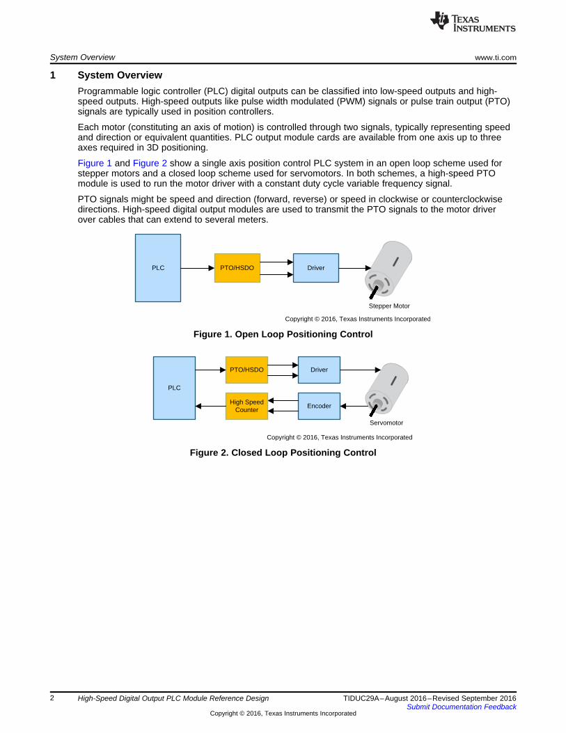
1 System OverviewProgrammable logic controller (PLC) digital outputs can be classified into low-speed outputs and high-speed outputs. High-speed outputs like pulse width modulated (PWM) signals or pulse train output (PTO)signals are typically used in position controllers.
Each motor (constituting an axis of motion) is controlled through two signals, typically representing speedand direction or equivalent quantities. PLC output module cards are available from one axis up to threeaxes required in 3D positioning.
Figure 1 and Figure 2 show a single axis position control PLC system in an open loop scheme used forstepper motors and a closed loop scheme used for servomotors. In both schemes, a high-speed PTOmodule is used to run the motor driver with a constant duty cycle variable frequency signal.
PTO signals might be speed and direction (forward, reverse) or speed in clockwise or counterclockwisedirections. High-speed digital output modules are used to transmit the PTO signals to the motor driverover cables that can extend to several meters.
Figure 1. Open Loop Positioning Control
Figure 2. Closed Loop Positioning Control
Copyright © 2016, Texas Instruments Incorporated
Digital Isolator
LineDriver
Protection
Isolated Power
Bea
gleB
one
Con
nect
or
Protection
3.3 V
Pulse input
4
5 V
5 V
4 OUT1
OUT4
Protection OUT2
Protection OUT3
Voltage converter
www.ti.com System Overview
3TIDUC29A–August 2016–Revised September 2016Submit Documentation Feedback
Copyright © 2016, Texas Instruments Incorporated
High-Speed Digital Output PLC Module Reference Design
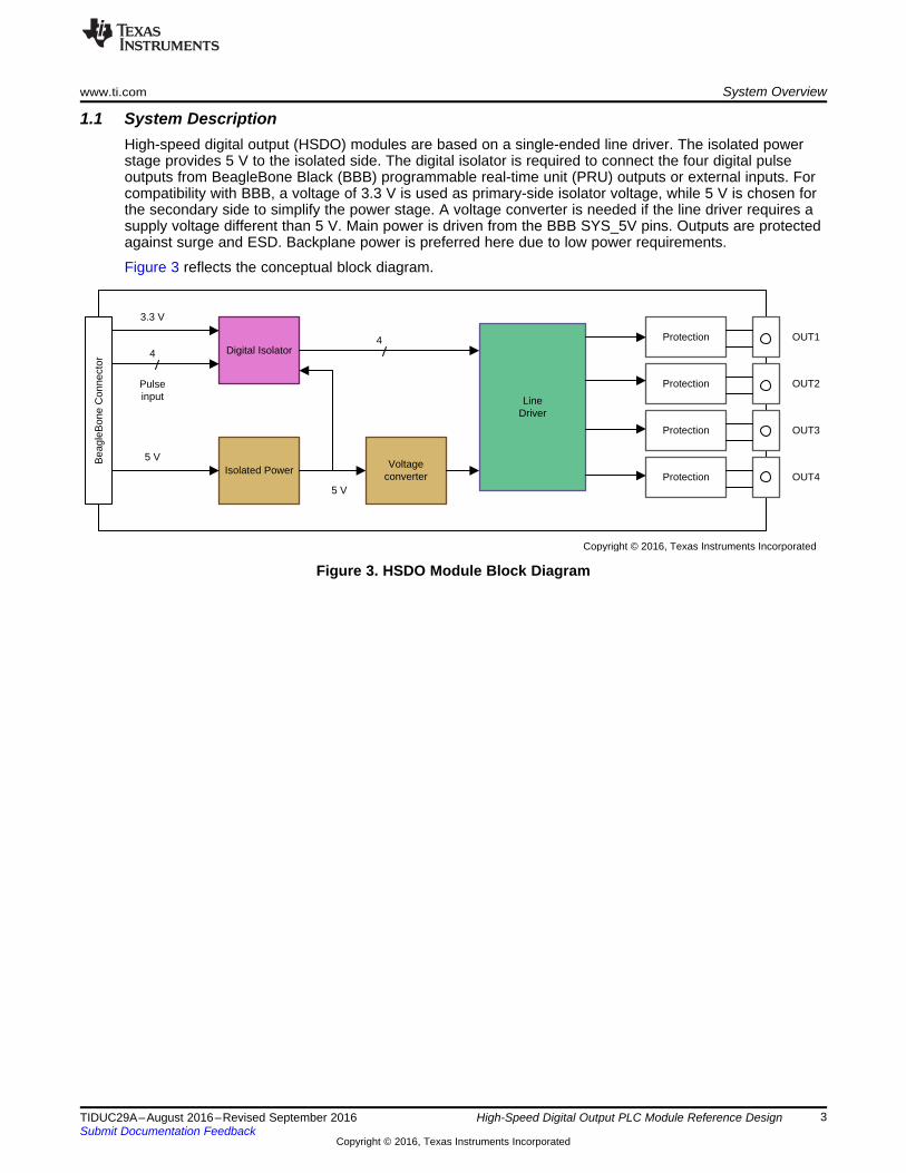
1.1 System DescriptionHigh-speed digital output (HSDO) modules are based on a single-ended line driver. The isolated powerstage provides 5 V to the isolated side. The digital isolator is required to connect the four digital pulseoutputs from BeagleBone Black (BBB) programmable real-time unit (PRU) outputs or external inputs. Forcompatibility with BBB, a voltage of 3.3 V is used as primary-side isolator voltage, while 5 V is chosen forthe secondary side to simplify the power stage. A voltage converter is needed if the line driver requires asupply voltage different than 5 V. Main power is driven from the BBB SYS_5V pins. Outputs are protectedagainst surge and ESD. Backplane power is preferred here due to low power requirements.
Figure 3 reflects the conceptual block diagram.
Figure 3. HSDO Module Block Diagram

Copyright © 2016, Texas Instruments Incorporated
ISO7140
DRV8803
Protection
SN6501
Bea
gleB
one
Con
nect
or
Protection
3.3 V
Pulse input
4
5 V
5 V
4 OUT1
OUT4
Protection OUT2
Protection OUT3
LM2765
10 V
Fault
System Overview www.ti.com
4 TIDUC29A–August 2016–Revised September 2016Submit Documentation Feedback
Copyright © 2016, Texas Instruments Incorporated
High-Speed Digital Output PLC Module Reference Design
1.2 Key System SpecificationsTable 1 lists the target specifications for the HSDO module. This design targets a single-ended output.See TI Design TIDA-00766 for a counterpart in differential-ended output implementation. To enable themodule to work with the TIDEP0027 reference design, the design is made in BBB cape format.
Table 1. Design Specifications
PARAMETER DETAILSNumber of outputs 2 channels, 4 single-ended outputs
Load type ohmic, opto-coupler inputs for step or servo amplifierLoad voltage 5 to 36 V external
Rated output current 125 mA rated, 500 mA max over temp rangeOutput signaling 5- to 36-V open drain
Load impedance 20 to 100 Ω: for 5-V supply;120 to 300 Ω: for 24-V supply
Frequency 100 Hz to 500 kHz: for 5-V external load;100 Hz to 200 kHz: for 24-V external load
Input duty cycle (mark/space ratio) 50% typicalCable length 10 m minimum
Electrical Isolation 2 kVPower source 5-V backplane power
Power consumption 0.5 W maximumTemperature range 0°C to 85°C
EMC protection
ESD: 12 kV IECContact: 15 kV HBM
EFT: 4 kVSurge: 1 kV
1.3 Block DiagramFigure 4 reflects the component selected in Section 2 as well as the signage LED components added tomonitor the availability of different power levels and input signals.
Figure 4. TIDA-00319 Block Diagram
www.ti.com Component Selection
5TIDUC29A–August 2016–Revised September 2016Submit Documentation Feedback
Copyright © 2016, Texas Instruments Incorporated
High-Speed Digital Output PLC Module Reference Design
2 Component Selection
2.1 Line DriverFor a targeted >10-m cable drive capability, single-ended high-speed driving is challenging. Higher speeddriving calls for higher driving capability as well as low load impedance, which means high powerconsumption.
Assuming load capacitance is around 5 nF including cable and receiver capacitance. If 1-MHz speed is tobe achieved and RC time constant of the load is to be kept below 0.1 in a period of 1 μs, a maximum loadof 20 Ω must be used. When full-swing driving is used (like CMOS or TTL) and to maintain the VOL andVOH levels, driver output impedance must be in the range of 1 Ω for proper voltage levels.
Such low impedance with industrial voltage level of 24 V would result in high current ( > 1 A) per outputand significant load power consumption (> 20 W). The high current is restricting the driver choice. Thehigh power requirement also limits the supply choice to the external field power supply. A low-side (LS)driver is suitable for these requirements. An LS switch allows for external power of the load and allows ahigher drive for the same package compared to push-pull drivers. To allow higher speed with reasonablepower, a restriction on the load supply voltage can be set (for example, 5 V) to limit both the power andmaximum current in the driver. Select the receiver on the other side to be sensitive to the falling edge asthe rising time is dominated by the load impedance.
Because this design will be used with the TIDEP0027, a direct output control is needed rather thanencoded input or serial interface. LS motor drivers is a suitable solution for single ended line drivers,search in the Stepper Motor with integrated FETs page would show a wide range of selection. TheDRV8803 is the best (and only valid) choice that provides four outputs direct interface. The DRV8803 is asmall form-factor device with four integrated low-side drivers with 0.5 A each of simultaneous RMS currentdriving with only PCB passive cooling.
2.2 Isolated PowerAmong the simplest topologies to realize the 5-V to 5-V isolated power is the push-pull DC-DC converter.There are almost no design equations. The push-pull driver SN6501 is a highly integrated driver. It islimited in output power, but for the application at hand where the line driver is relying on the external loadpower, the power requirement is way below the SN6501 maximum limit.
2.3 Voltage ConverterThe DRV8803 works with a voltage supply in the range of 9 to 60 V. As this design will use external loadpower, the driver voltage is only used for gate driving. A voltage level as low as 8.3 V can still switch thegate with a little bit of higher driver impedance. Given that the DRV8803 requires a maximum < 2.1 mA tooperate, one of the simplest power solutions is using a voltage doubler (charge pump) as a voltageconverter. With a 5-V input, a stable 10-V output is generated using the charge pump given light load. TheLM2765 is a switched capacitor voltage converter running with a supply voltage in the range of 1.8 to 5.5V with 90% efficiency at a 20-mA load. Compared to the alternative boost converters, the switchedcapacitor solution is much more compact and cost effective.
2.4 Digital IsolatorThe ISO7140 is selected as a four-channel digital isolator. The ISO714x family provides galvanic isolationat 2500 VRMS for 1 minute per UL or 4242 VPK per VDE. The selected isolators support up to 50 Mbps,which is well above the communication speed used in this TI Design.

Thermal
Shut down
OUT1
GND
(multiple pins)
VCLAMP
IN1
IN2
IN3
Internal
Reference
Regs
UVLO
Int. VCC
nFAULT
Control
Logic
IN4
nENBL
VMLS Gate
Drive
OUT2
OUT3
OUT4
OCP
&
Gate
Drive
8.2V – 60V
OCP
&
Gate
Drive
OCP
&
Gate
Drive
OCP
&
Gate
Drive
8.2V – 60V
Optional
Zener
Inductive
Load
Inductive
Load
Inductive
Load
Inductive
Load
RESET
Copyright © 2016, Texas Instruments Incorporated
Getting Started Hardware www.ti.com
6 TIDUC29A–August 2016–Revised September 2016Submit Documentation Feedback
Copyright © 2016, Texas Instruments Incorporated
High-Speed Digital Output PLC Module Reference Design
3 Getting Started Hardware
3.1 DRV8803 DriverThe DRV8803 is a four-channel low-side driver with overcurrent protection. It has built-in diodes to clampturnoff transients generated by inductive loads and can be used to drive unipolar stepper motors, DCmotors, relays, solenoids, or other loads like cables and resistive loads as in our design. The DRV8803can supply up to a 0.8-A continuous current per channel with all channels turned on at 25°C with passivePCB heat sinking. Being controlled through a simple parallel interface allows it to work with existingTIDEP0027 PTOs.
Internal shutdown functions are provided for overcurrent protection, short-circuit protection, undervoltagelockout, over-temperature protection, and faults are indicated by a fault output pin. A 16-pin HTSSOPpackage is used for its compact layout.
The DRV8803 can withstand power supply voltage up to 65 V, giving more flexibility in field power supplyselection and a more robust application.
Figure 5 shows the internal structure of the DRV8803. The four-input parallel interface (IN1 to IN4) can bedisabled by nENBL pin. nFAULT indicates fault conditions, which requires RESET assertion to restoreoperation. VCLAMP is used to clamp output voltage to a certain level or to the field supply level.
Figure 5. DRV8803 Functional Block Diagram

IN
1T
f=
LOAD LOADR Ct = ´
OH FIELD OFF LOADV V I R= - ´
OL R DSV I r= ´
FIELD
R
L
VI
R=
2
FIELD
R
L
VP D
R=
Copyright © 2016, Texas Instruments Incorporated
IN (fIN)
OUTVSUPPLY
CLOAD
RLOAD
VFIELD
VOH = VFIELD
VOL
2�
ILS
www.ti.com Getting Started Hardware
7TIDUC29A–August 2016–Revised September 2016Submit Documentation Feedback
Copyright © 2016, Texas Instruments Incorporated
High-Speed Digital Output PLC Module Reference Design
3.1.1 External LoadExternal load (resistive and capacitive) is calculated here within the limits of low side maximum currentand reasonable power dissipation as well as maximum expected frequency.
Figure 6. TIDA-00319 Driver Load Circuit
Figure 6 illustrates the load circuit connected to the LS driver. The output waveform is also plotted inFigure 6. Use these simple equations to calculate the different design parameters:• Average load power
(1)where D is the duty cycle of the input signal (50% in case of PTO)
• Load current when VOUT is low
(2)• Output low level
(3)where low-side switch resistance is 0.4 to 0.8 Ω for a low VSUPPLY
• Output high level(4)
as IOFF is in the μA range, consider VOH = VFIELD
• Time constant of the rising edge(5)
• Period
(6)

VM1
VCLAMP2
OUT13
OUT24
GND5
OUT36
OUT47
ENBL8
RESET9
IN410
IN311
GND12
IN213
IN114
NC15
FAULT16
PAD17
U6
DRV8803PWPR
GND_ISO
2mA
1A max
overcurrent,shortcircuit,undervoltage,overtemp.
uA Iin
36V
D15
SMBJ36A-13-F
GND_ISO
GND_ISO
DisableGND_ISO
0.1µFC15
0.1µFC16
VDD_10V_ISO
OUTA
OUTB
OUTC
OUTDRed
12
D16
3.9kR20
1.6mA , 1.6V@low current
3.9k
R23DNP
VDD_5V_ISO
3.9k
R22
Copyright © 2016, Texas Instruments Incorporated
Getting Started Hardware www.ti.com
8 TIDUC29A–August 2016–Revised September 2016Submit Documentation Feedback
Copyright © 2016, Texas Instruments Incorporated
High-Speed Digital Output PLC Module Reference Design
Assuming the maximum frequency of 500 kHz, and assuming t = T/10 and 4 nF of the total load includingthe cable, this results in a maximum load of 50 Ω.
If targeting a lower frequency such as 200 kHz, use a higher impedance of 120 Ω. Assuming a field supplyof 5 V and a load of 40 Ω, a maximum current of 125 mA and an average power of 0.3125 W is calculatedfor one channel.
Assuming a field supply of 24 V and a load of 100 Ω, a maximum current of 240 mA and an averagepower of 2.9 W is calculated for one channel. This shows the high power requirement of a high fieldsupply, which prevents high-speed operation on that field supply level.
With the given current calculations, and assuming worst case switch resistance of 0.8 Ω, a worst caseoutput low level would be ~0.1 V for a 5-V supply, and ~0.2 V for the 24-V supply; this does not includereflection and other signal distortion aspects.
3.1.2 Clamp DiodeThe DRV8803 has internal diodes to a common clamping pin. This pin allows setting a clamping voltagedifferent from the operating voltage set by external Zener diode. Unlike the application circuit in theDRV8803 datasheet (SLVSAW5), the Zener diodes are connected between the clamping point andground. This connection guarantees independence of the low voltage supply used (10 V) and theclamping voltage (rated field supply, for example, 36 V max).
The unidirectional SMB TVS diode with a 36-V reverse standoff voltage is used. This allows the usage ofhigh field supply with low power supply for the driver, still protecting the driver from surges and othertransient events.
Figure 7. DRV8803 Output Driver Schematic

65V max
36V
D17
SM
BJ36
A-1
3-F
GND_ISO
36V
D18
SM
BJ36A
-13-F
GND_ISO
GND_ISO
100pFC17
GND_ISO
100pFC19
GND_ISO
4
1
2
3
J8
1844236
Earth
1000pF
C18
GND_ISOEarth
Copyright © 2016, Texas Instruments Incorporated
www.ti.com Getting Started Hardware
9TIDUC29A–August 2016–Revised September 2016Submit Documentation Feedback
Copyright © 2016, Texas Instruments Incorporated
High-Speed Digital Output PLC Module Reference Design
3.1.3 Thermal ConsiderationsAt its peak power dissipation, an area of about 15 cm2 per DRV8803 device would suffice to operate atambient temperatures of 85°C with only PCB cooling. The layout design provides around 26-cm2 copperon the top layer, and 33 cm2 on the bottom layer per device. The thermal management should not be anissue at all, and the layout area can be further reduced if smaller footprint is required.
3.1.4 ProtectionIn addition to the clamp diode, similar diodes are placed at each output for protection against electricaltransient. Same unidirectional SMB TVS diode with a 36-V reverse standoff voltage is used for eachoutput plus a 100-pF output capacitor to reduce the output transient time and enhance signal properties.Figure 8 shows the TVS diodes on a couple of outputs.
Figure 8. Protection TVS Diodes for Two Outputs

Vcc
GNDGND
D2
SN6501
D1S
S
G2
G1
fOSC Freq.
DividerOSC
BBM
LogicQ1
Q2
Q1 on Q2 on
Q2 off
tBBM
Q1 off
Getting Started Hardware www.ti.com
10 TIDUC29A–August 2016–Revised September 2016Submit Documentation Feedback
Copyright © 2016, Texas Instruments Incorporated
High-Speed Digital Output PLC Module Reference Design
3.2 Isolated PowerThe SN6501 is a monolithic oscillator and power-driver, specifically designed for small form factor, isolatedpower supplies in isolated interface applications. The device drives a low-profile, center-tappedtransformer primary from a 3.3-V or 5-V DC power supply. The secondary can be wound to provide anyisolated voltage based on transformer turns ratio.
The SN6501 is a transformer driver designed for low-cost, small form-factor, isolated DC-DC convertersusing the push-pull topology. The device includes an oscillator that feeds a gate-drive circuit. The gatedrive, comprising a frequency divider and a break-before-make (BBM) logic, provides two complementaryoutput signals, which alternately turn the two output transistors on and off.
Figure 9. SN6501 Block Diagram
The output frequency of the oscillator is divided down by an asynchronous divider that provides twocomplementary output signals, S and S, with a 50% duty cycle. A subsequent BBM logic inserts a deadtime between the high pulses of the two signals.
The switching frequency for the 5-V input is in the range of 300 to 600 kHz with 400 kHz nominal. Thepush-pull driver is an unregulated supply, which is acceptable if the input voltage range is limited, and theload range is also limited. In this TI Design, the load is almost constant regardless of the input activity andoutput driver load.
The push-pull stage design consists of:• Diode selection• Capacitor selection• Transformer selection
3.2.1 Diode SelectionA diode is chosen to minimize the forward voltage to maximize secondary voltage and minimize powerdissipation. In a high-frequency application like using with the SN6501, a short recovery time is alsorequired. Diode breakdown voltage must exceed the output voltage, and maximum current handling mustexceed maximum current in the switch. A good choice for low-volt applications and ambient temperaturesof up to 85°C is the low-cost Schottky rectifier MBR0520L with a typical forward voltage of 275 mV at a100-mA forward current.
3.2.2 Capacitor SelectionTwo capacitor components are required at the output of the push-pull stage: a bypass capacitor with lowimpedance at high frequencies, typically in the range of 10 to 100 nF, and a bulk capacitor at the rectifieroutput to smooth output voltage, which is at least 10 µF. 22 µF plus 0.1-µF caps are used at the output.An input bulk capacitor at the center tap of the primary supports large currents into the primary during thefast switching transients. To minimize ripple, two capacitors (1 μF and 10 μF) are used.

Copyright © 2016, Texas Instruments Incorporated
Oscillator divided by two
GNDCAPí
S3
GND
C2
VOUT = 2 V+
S1CAP+
S2
C1
S4
V+
475µH
6
5
1
2
3 4
T1
D11
MBR0520LT1G
D12
MBR0520LT1G
D11
VCC2
D23
GND4
GND5
U5
SN6501QDBVRQ1
GND_ISO
22µFC13
0.1µFC14
DGND
GND_ISO
VDD_5V_ISO
21 Green
D14LTST-C150KGKT
GND_ISO
DGND
10µFC11
1µFC10
TR_P
TR_N
2.2kR9
SYS_5V
TP_5V_ISO
Copyright © 2016, Texas Instruments Incorporated
www.ti.com Getting Started Hardware
11TIDUC29A–August 2016–Revised September 2016Submit Documentation Feedback
Copyright © 2016, Texas Instruments Incorporated
High-Speed Digital Output PLC Module Reference Design
3.2.3 Transformer SelectionTransformer design parameters include the V-t product to prevent transformer from saturation and turnsratio to deliver the output voltage in presence of the diode drop. Maximum power and isolation voltage areother two parameters to consider when selecting. For more details about transformers and othercomponents selection, see SN6501 datasheet (SLLSEA0).
Figure 10. Push-Pull Circuit Schematic
3.3 Charge Pump Voltage ConverterThe LM2765 CMOS charge-pump voltage converter operates as a voltage doubler for an input voltage inthe range of 1.8 to 5.5 V. Two low-cost capacitors and a diode are used in this circuit to provide an outputcurrent of up to 20 mA.
The operating principle is shown in Figure 11. Input voltage is stored on capacitor C1 in one phase, and inthe next phase this voltage is added to the input voltage to generate double the voltage at the output.
Figure 11. Voltage Doubling Principle

SD4
V+1
GND2
C1+6
C1-3
OUT5
U3
LM2765M6
VDD_5V_ISO
3.3µFC7
5.6V
D7
BZT52C5V6T-7
VDD_10V_ISO
21 Green
D10LTST-C150KGKT
GND_ISO
20mA max
3.3µFC6
GND_ISO
0.1
R14
GND_ISO
3.3µFC8
GND_ISO
2.2kR15
TP_10V_ISO
GND_ISO
5.6V
D13BZT52C5V6T-7
22R18
Copyright © 2016, Texas Instruments Incorporated
O
RIPPLE O C2
OSC 2
IV 2 I ESR
f C= + ´ ´
´
OUT SW C1 C2
OSC 1
2R 2R 4 ESR ESR
f C@ + + +
´
Getting Started Hardware www.ti.com
12 TIDUC29A–August 2016–Revised September 2016Submit Documentation Feedback
Copyright © 2016, Texas Instruments Incorporated
High-Speed Digital Output PLC Module Reference Design
The LM2765 operates at a 50-kHz switching frequency to reduce output resistance and voltage ripple withan operating current of only 130 μA (operating efficiency greater than 90% with most loads) and 0.1-μAtypical shutdown current.
One important design parameter in the charge pump circuit is the output resistance, which is a function ofthe switch resistance, oscillator frequency, pumping capacitor C1, and output capacitor C2.
(7)
RSW is typically 8 Ω in the LM2765. Equation 7 shows the benefit of increasing the switching frequencyand selecting low ESR capacitors to reduce the output resistance.
Output ripple voltage is a function of the load current, switching frequency, output capacitance, and itseffective series resistance.
(8)
A high capacitance, low ESR reduces both the output ripple and the output resistance.
The diode connecting input and output only needs to protect the device from turning on its own parasiticdiode and potentially latching up. During start-up, D1 will also quickly charge up the output capacitor toVIN minus the diode drop, thereby decreasing the start-up time. Therefore, the diode D1 must haveenough current carrying capability to charge the output capacitor at start-up, as well as a low forwardvoltage to prevent the internal parasitic diode from turning on. Instead of a using a typical Schottky diode,a Zener diode BZT52C5V6T-7 is used. The purpose of this Zener is to prevent the voltage from exceeding2× the input voltage as a simple regulating method.
The same method is used at the input side, where the same Zener diode of the 5.6-V reverse breakdownis used to regulate the push-pull output and ensure the maximum input voltage of the charge pumpLM2765 is not exceeded.
Figure 12. Charge Pump Doubler Schematic
LeCroy WaveSurfer 454
Agilent E3631A Power Supply
TIDA-00319
Agilent 33120A Waveform Generator
In1
3.3 V 5 V
out1
VFIELD
LeCroy WaveSurfer 454
Agilent E3631A Power Supply
CLOAD
In1
330 �F
RLOAD
www.ti.com Testing and Results
13TIDUC29A–August 2016–Revised September 2016Submit Documentation Feedback
Copyright © 2016, Texas Instruments Incorporated
High-Speed Digital Output PLC Module Reference Design
4 Testing and Results
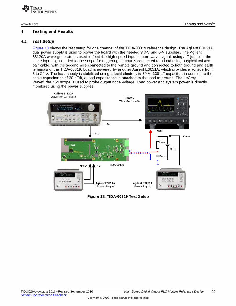
4.1 Test SetupFigure 13 shows the test setup for one channel of the TIDA-00319 reference design. The Agilent E3631Adual power supply is used to power the board with the needed 3.3-V and 5-V supplies. The Agilent33120A wave generator is used to feed the high-speed input square wave signal, using a T-junction, thesame input signal is fed to the scope for triggering. Output is connected to a load using a typical twistedpair cable, with the second wire connected to the remote ground and connected to both ground and earthterminals of the TIDA-00319. Load is powered by another Agilent E3631A, which provides a voltage from5 to 24 V. The load supply is stabilized using a local electrolytic 50-V, 330-μF capacitor. in addition to thecable capacitance of 30 pF/ft, a load capacitance is attached to the load to ground. The LeCroyWavefurfer 454 scope is used to probe output node voltage. Load power and system power is directlymonitored using the power supplies.
Figure 13. TIDA-00319 Test Setup
Copyright © 2016, Texas Instruments Incorporated
IN (500 kHz)
OUT10 V
1 nF
44 �
5 V
15-m cable
Testing and Results www.ti.com
14 TIDUC29A–August 2016–Revised September 2016Submit Documentation Feedback
Copyright © 2016, Texas Instruments Incorporated
High-Speed Digital Output PLC Module Reference Design
4.1.1 Test ProcedureAn output waveform as well as rise and fall times, output delay, output delay variation, output high, outputlow levels, system, and load power are measured for different input frequencies as well as different fieldvoltages. High field voltage is limited only to lower input frequency for limiting power of the load.
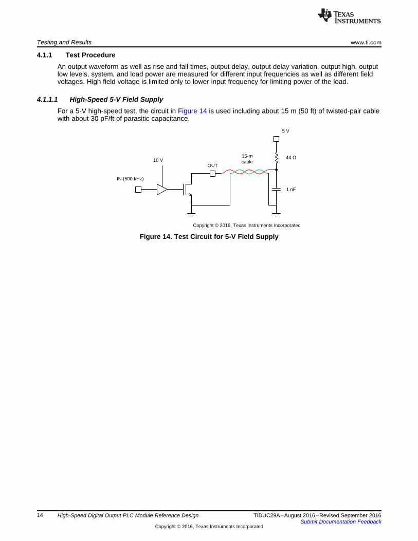
4.1.1.1 High-Speed 5-V Field SupplyFor a 5-V high-speed test, the circuit in Figure 14 is used including about 15 m (50 ft) of twisted-pair cablewith about 30 pF/ft of parasitic capacitance.
Figure 14. Test Circuit for 5-V Field Supply

www.ti.com Testing and Results
15TIDUC29A–August 2016–Revised September 2016Submit Documentation Feedback
Copyright © 2016, Texas Instruments Incorporated
High-Speed Digital Output PLC Module Reference Design
Table 2 lists the test results of the 500-kHz signal input. The cable effect on the signal waveform is shownin Figure 15, which clearly shows large undershoot. Lower overshoot levels can be achieved by reducingthe transition times using a higher load capacitor close to the driver. The higher low-voltage level is due tocable impedance. 400 mV is still acceptable even for the standard TTL and CMOS logic.
Table 2. Test Results at VFIELD = 5 V With 15-m Cable
PARAMETER VALUEBackplane power consumption 5 V: 37 mA , 3.3 V: 8 mA
Field power consumption Average current = 60 mARise time 20% to 80% 93 nsFall time 80% to 20% 78 ns
Output low level 431 mVOutput high level 5 V
Overshoot + 1.8%Overshoot – 3.5%
Figure 15. Output Waveform at 500 kHz With 15-m Cable

Testing and Results www.ti.com
16 TIDUC29A–August 2016–Revised September 2016Submit Documentation Feedback
Copyright © 2016, Texas Instruments Incorporated
High-Speed Digital Output PLC Module Reference Design
The test is repeated with the cable removed to have transition times measured. Capacitive load is alsoremoved. Low level voltage is lower as expected and transition times are about the half of the previoustest. Rise and fall times are symmetric, which shows the attached direct capacitive load is at anappropriate value.
Table 3. Test Results at VFIELD = 5 V, No Cable
PARAMETER VALUERise time 20% to 80% 50 nsFall time 80% to 20% 47 ns
Output low level 131 mVOutput high level 5 V
Overshoot + 3.8%Overshoot – 2.9%
Figure 16. Output Waveform Without Cable at 500 kHz

www.ti.com Testing and Results
17TIDUC29A–August 2016–Revised September 2016Submit Documentation Feedback
Copyright © 2016, Texas Instruments Incorporated
High-Speed Digital Output PLC Module Reference Design
The delay variation of the driver is shown in Figure 17. The delay itself is due to the isolator and the driveras well as external load. The delay variation, though, is solely a function of the DRV8803 driver. This isone of the limiting factors (among other factors mentioned earlier) that limits the maximum frequency ofoperation in the case of a single-ended driver.
Table 4. Delay Variation at VFIELD = 5 V, No Cable
PARAMETER VALUERising delay 550 nsFalling delay 430 ns
Rising delay variation 144 nsFalling delay variation 144 ns
Minimum output duty cycle 40.5 %Maximum output duty cycle 48.3 %
Figure 17. Delay Variation of Output Driver
Testing and Results www.ti.com
18 TIDUC29A–August 2016–Revised September 2016Submit Documentation Feedback
Copyright © 2016, Texas Instruments Incorporated
High-Speed Digital Output PLC Module Reference Design
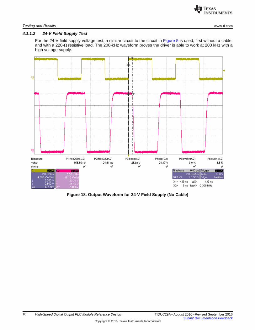
4.1.1.2 24-V Field Supply TestFor the 24-V field supply voltage test, a similar circuit to the circuit in Figure 5 is used, first without a cable,and with a 220-Ω resistive load. The 200-kHz waveform proves the driver is able to work at 200 kHz with ahigh voltage supply.
Figure 18. Output Waveform for 24-V Field Supply (No Cable)
www.ti.com Testing and Results
19TIDUC29A–August 2016–Revised September 2016Submit Documentation Feedback
Copyright © 2016, Texas Instruments Incorporated
High-Speed Digital Output PLC Module Reference Design
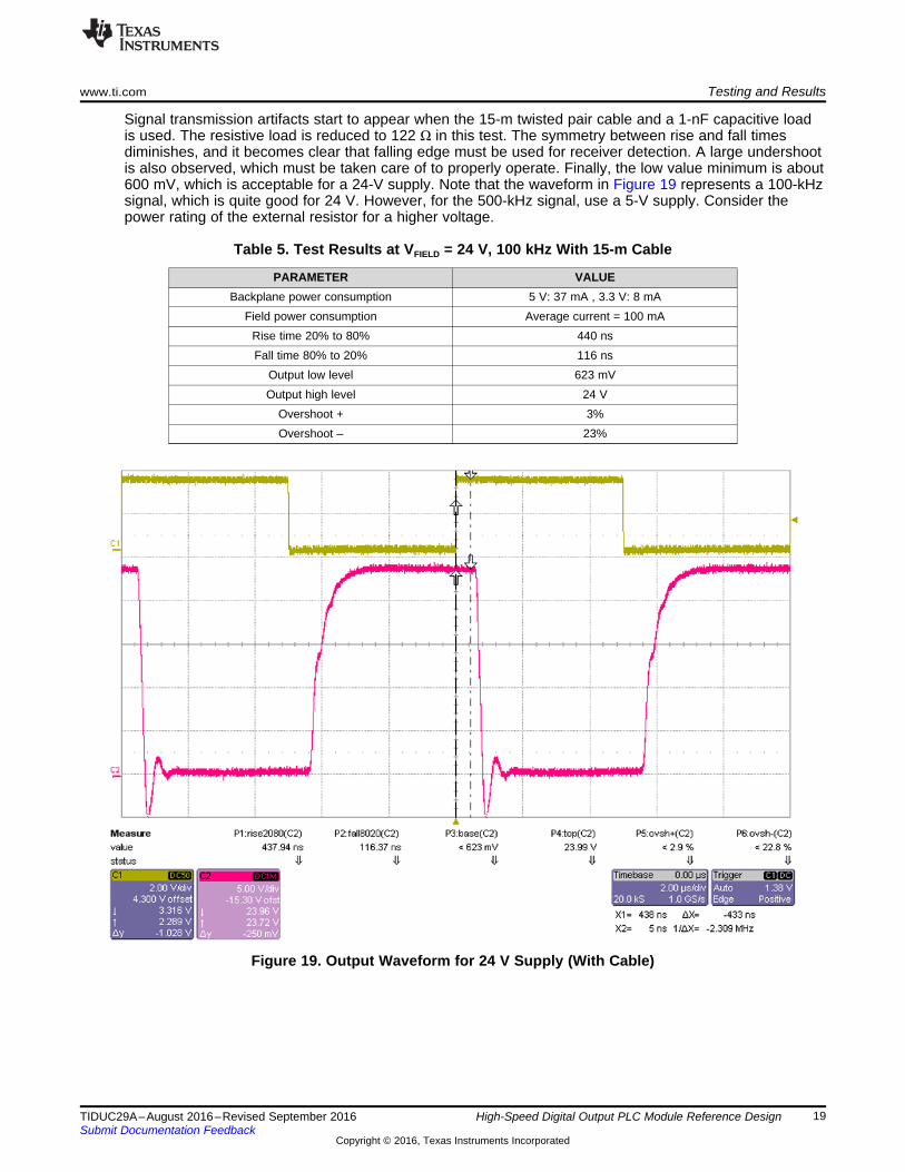
Signal transmission artifacts start to appear when the 15-m twisted pair cable and a 1-nF capacitive loadis used. The resistive load is reduced to 122 Ω in this test. The symmetry between rise and fall timesdiminishes, and it becomes clear that falling edge must be used for receiver detection. A large undershootis also observed, which must be taken care of to properly operate. Finally, the low value minimum is about600 mV, which is acceptable for a 24-V supply. Note that the waveform in Figure 19 represents a 100-kHzsignal, which is quite good for 24 V. However, for the 500-kHz signal, use a 5-V supply. Consider thepower rating of the external resistor for a higher voltage.
Table 5. Test Results at VFIELD = 24 V, 100 kHz With 15-m Cable
PARAMETER VALUEBackplane power consumption 5 V: 37 mA , 3.3 V: 8 mA
Field power consumption Average current = 100 mARise time 20% to 80% 440 nsFall time 80% to 20% 116 ns
Output low level 623 mVOutput high level 24 V
Overshoot + 3%Overshoot – 23%
Figure 19. Output Waveform for 24 V Supply (With Cable)

Design Files www.ti.com
20 TIDUC29A–August 2016–Revised September 2016Submit Documentation Feedback
Copyright © 2016, Texas Instruments Incorporated
High-Speed Digital Output PLC Module Reference Design
5 Design Files
5.1 SchematicsTo download the Schematics for each board, see the design files at TIDA-00319.
5.2 Bill of MaterialsTo download the Bill of Materials for each board, see the design files at TIDA-00319.
5.3 Layout PrintsTo download the Layout Prints for each board, see the design files at TIDA-00319.
5.4 Altium ProjectTo download the Altium project files for each board, see the design files at TIDA-00319.
5.5 Gerber FilesTo download the Gerber files for each board, see the design files at TIDA-00319.
5.6 Assembly DrawingsTo download the Assembly Drawings for each board, see the design files at TIDA-00319.
6 About the AuthorAHMED NOEMAN is a system engineer at Texas Instruments Germany developing reference designsolutions for industrial applications. Ahmed has many years of experience in analog and RF design, AMSmodeling, and verification as well as application and system engineering in a wide range of fields includingRF transceivers, clocks and PLLs, memory systems, and others. Ahmed received his BSC and MSEEfrom Ain Shams University, Egypt.
www.ti.com Revision A History
21TIDUC29A–August 2016–Revised September 2016Submit Documentation Feedback
Copyright © 2016, Texas Instruments Incorporated
Revision History
Revision A HistoryNOTE: Page numbers for previous revisions may differ from page numbers in the current version.
Changes from Original (August 2016) to A Revision ..................................................................................................... Page
• Changed from preview draft ............................................................................................................. 1

IMPORTANT NOTICE FOR TI REFERENCE DESIGNS
Texas Instruments Incorporated (‘TI”) reference designs are solely intended to assist designers (“Designer(s)”) who are developing systemsthat incorporate TI products. TI has not conducted any testing other than that specifically described in the published documentation for aparticular reference design.TI’s provision of reference designs and any other technical, applications or design advice, quality characterization, reliability data or otherinformation or services does not expand or otherwise alter TI’s applicable published warranties or warranty disclaimers for TI products, andno additional obligations or liabilities arise from TI providing such reference designs or other items.TI reserves the right to make corrections, enhancements, improvements and other changes to its reference designs and other items.Designer understands and agrees that Designer remains responsible for using its independent analysis, evaluation and judgment indesigning Designer’s systems and products, and has full and exclusive responsibility to assure the safety of its products and compliance ofits products (and of all TI products used in or for such Designer’s products) with all applicable regulations, laws and other applicablerequirements. Designer represents that, with respect to its applications, it has all the necessary expertise to create and implementsafeguards that (1) anticipate dangerous consequences of failures, (2) monitor failures and their consequences, and (3) lessen thelikelihood of failures that might cause harm and take appropriate actions. Designer agrees that prior to using or distributing any systemsthat include TI products, Designer will thoroughly test such systems and the functionality of such TI products as used in such systems.Designer may not use any TI products in life-critical medical equipment unless authorized officers of the parties have executed a specialcontract specifically governing such use. Life-critical medical equipment is medical equipment where failure of such equipment would causeserious bodily injury or death (e.g., life support, pacemakers, defibrillators, heart pumps, neurostimulators, and implantables). Suchequipment includes, without limitation, all medical devices identified by the U.S. Food and Drug Administration as Class III devices andequivalent classifications outside the U.S.Designers are authorized to use, copy and modify any individual TI reference design only in connection with the development of endproducts that include the TI product(s) identified in that reference design. HOWEVER, NO OTHER LICENSE, EXPRESS OR IMPLIED, BYESTOPPEL OR OTHERWISE TO ANY OTHER TI INTELLECTUAL PROPERTY RIGHT, AND NO LICENSE TO ANY TECHNOLOGY ORINTELLECTUAL PROPERTY RIGHT OF TI OR ANY THIRD PARTY IS GRANTED HEREIN, including but not limited to any patent right,copyright, mask work right, or other intellectual property right relating to any combination, machine, or process in which TI products orservices are used. Information published by TI regarding third-party products or services does not constitute a license to use such productsor services, or a warranty or endorsement thereof. Use of the reference design or other items described above may require a license from athird party under the patents or other intellectual property of the third party, or a license from TI under the patents or other intellectualproperty of TI.TI REFERENCE DESIGNS AND OTHER ITEMS DESCRIBED ABOVE ARE PROVIDED “AS IS” AND WITH ALL FAULTS. TI DISCLAIMSALL OTHER WARRANTIES OR REPRESENTATIONS, EXPRESS OR IMPLIED, REGARDING THE REFERENCE DESIGNS OR USE OFTHE REFERENCE DESIGNS, INCLUDING BUT NOT LIMITED TO ACCURACY OR COMPLETENESS, TITLE, ANY EPIDEMIC FAILUREWARRANTY AND ANY IMPLIED WARRANTIES OF MERCHANTABILITY, FITNESS FOR A PARTICULAR PURPOSE, AND NON-INFRINGEMENT OF ANY THIRD PARTY INTELLECTUAL PROPERTY RIGHTS.TI SHALL NOT BE LIABLE FOR AND SHALL NOT DEFEND OR INDEMNIFY DESIGNERS AGAINST ANY CLAIM, INCLUDING BUT NOTLIMITED TO ANY INFRINGEMENT CLAIM THAT RELATES TO OR IS BASED ON ANY COMBINATION OF PRODUCTS ASDESCRIBED IN A TI REFERENCE DESIGN OR OTHERWISE. IN NO EVENT SHALL TI BE LIABLE FOR ANY ACTUAL, DIRECT,SPECIAL, COLLATERAL, INDIRECT, PUNITIVE, INCIDENTAL, CONSEQUENTIAL OR EXEMPLARY DAMAGES IN CONNECTION WITHOR ARISING OUT OF THE REFERENCE DESIGNS OR USE OF THE REFERENCE DESIGNS, AND REGARDLESS OF WHETHER TIHAS BEEN ADVISED OF THE POSSIBILITY OF SUCH DAMAGES.TI’s standard terms of sale for semiconductor products (http://www.ti.com/sc/docs/stdterms.htm) apply to the sale of packaged integratedcircuit products. Additional terms may apply to the use or sale of other types of TI products and services.Designer will fully indemnify TI and its representatives against any damages, costs, losses, and/or liabilities arising out of Designer’s non-compliance with the terms and provisions of this Notice.IMPORTANT NOTICE
Mailing Address: Texas Instruments, Post Office Box 655303, Dallas, Texas 75265Copyright © 2016, Texas Instruments Incorporated


![High-efficiency Operation, Outstanding Performance · VF200 is used to control the speed of motor, ultimately the pressure of pump. Use PLC [FP-X] to output speed command (0 to 10V](https://img.dokumen.tips/doc/110x75/5f1f4303b7bbf31c191570d9/high-efficiency-operation-outstanding-performance-vf200-is-used-to-control-the.jpg)