Embed Size (px)
Citation preview
High-resolution timing inphoton detection – a new
frontier in physics ?
J. Va’vra, SLAC
Light travels 300µm in one ps

11/14/07 J. Va'vra, Photon Detectors, AISSLAC
2
Some photon detectors in the past 10-20 years:MCP-PMT
MaPMT
HAPD
Mesh PMT
G-APD (SiPMT) Multi-GEM
Micromegas+MCP
GEM+MHSPGEM+MHSP
127 mm
ReFerencReFerenc
PMT+G-APDPMT+G-APD
SLD CRID
DELPHI
OMEGA
CERES
G-APDs
College de France
Cornell RICH
JETSET
MCP-PMTMCP-PMT
HPDMCP-PMT
11/14/07 J. Va'vra, Photon Detectors, AISSLAC
3
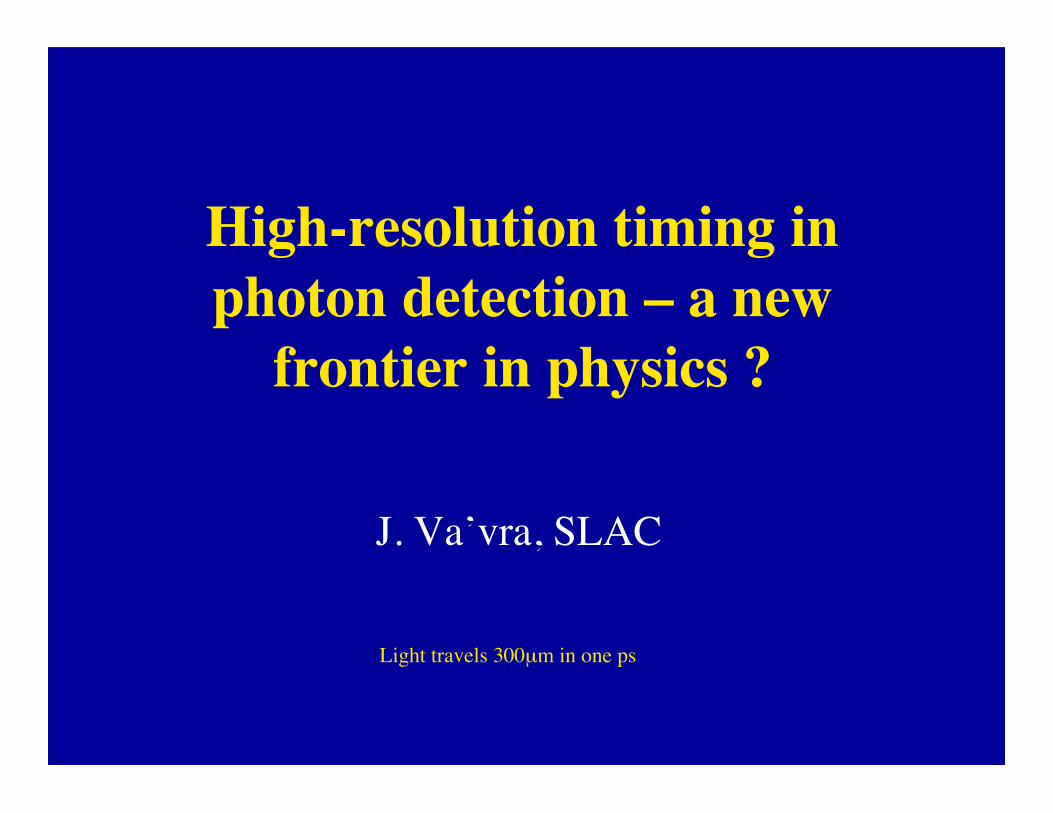
Content• Aim of the talk is to explore high resolution timing• Basic properties of the photon detectors:
(TTS, Photocathodes, PDE = photon detection efficiency, timing tails, etc.)• Timing strategies:
- double-threshold timing, time-over-threshold timing, waveform sampling, CFD.• Compare timing results for these detector:
- Vacuum-based photon detectors with micro-channel plates (MCP-PMT)- Silicone photon detectors (APD) operating in a Geiger mode (G-APD)- Hybrid photon detectors, combining vacuum and APD detector (HAPD)
• Examples of applications:- CMS and Atlas TOF detector for FP420 experiments at LHC: goal is σ ~ 10-15 ps- TOF for Super B Forward PID: goal is σ ~ 15-20 ps- Focusing DIRC for Super B to tag Cherenkov photon color: goal is σ ~ 150 ps- TOP DIRC at Super B at KEK to measure photon coordinate: goal is σ ~ 50 ps- Add a TOF capability to the PET machines in medicine: goal is σ ~ 30-50 ps.- The astrophysics detectors such as MAGIC: goal is σ ~ 100-200 ps (or even less ???)
• Institution interested in a high resolution timing at present:- Nagoya U.,KEK, Saclay, U. of Chicago, Argonne lab, Fermi lab, Arlington U., SLAC, etc.
11/14/07 J. Va'vra, Photon Detectors, AISSLAC
4
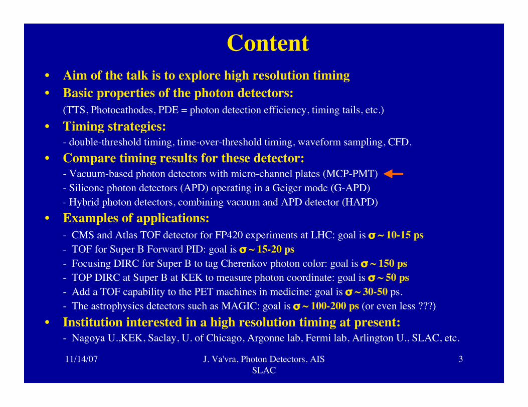
A bit of history of a high resolution timing• ~35 years ago:
Helmuth Spieler of LBL (private communication):Built, as a part of his Ph.D. thesis work, a TOF system using MCPs for an experiment detectingheavy ions. He routinely achieved a timing resolution of σ ~ 20-30 ps.
- ~27 years ago:Bill Attwood of SLAC (lecture on the TOF technique at SLAC in 1980):The lecture series did not even mention MCP-PMTs. The technology clearly existed at thattime, but was either not affordable or obtainable or simply ignored for large scale applications.
• ~10 years ago:Crispin Williams of CERN proposes a TOF detector for ALICE based on multi-gap glass-basedRPC chambers; test beam results indicate resolution of σ ~ 40-50 ps/track.
• ~ 4 years ago:Henry Frisch of Univ. of Chicago (the 1-st proposal for a 1 ps timing with a MCP-PMTscoupled to a Cherenkov radiator):Aspen talk in 2003, and Credo et al., IEEE Nucl. Sci. Symp., Conf. Records, Vol. 1 (2004).
• ~2 years ago:Takayoshi Ohshima’s group in University of Nagoya (reached a σ ~ 6.2 ps in the test beam)“The Pico-Sec Timing Workshop,” 18 Nov 2005, U. of Chicago, http://hep.uchicago.edu/psec/.

11/14/07 J. Va'vra, Photon Detectors, AISSLAC
5
What are the reasons to push the TOFtechnique towards the new limits ?
• Fast Cherenkov light rather than a scintillation
• New detectors with a small transit time spread (TTS)
• Fast electronics is easily available even from catalogues(amplifiers, splitters, cables, etc., in 1-19 GHz BW range)
• New optics available for testing (fast laser diodes, fiber optics,light splitters, etc.)

11/14/07 J. Va'vra, Photon Detectors, AISSLAC
6
Issues important for fast photon detectors ?
• Photon Detection Efficiency (PDE).• Transit time spread (σTTS).• Detector design.• Current best experimental timing results.• Degradation of performance in magnetic field.• Bad effects (aging, rate effects, cross-talk, bad ground return, etc.).• Systematic effects (start time error, tracking, drifts, etc.).• Pixilization and its effect on timing.• Electronics.• Reliability and affordability.
Will concentrate on these issuesin this talk.
water
iceberg

Photon Detection Efficiency
PDE = QE x εpe collection x εdetection x εpacking geometry
Examples of typical PDE values at present:1. PMT: > 20%
2. Multi-pixel G-APD: ≥ 40%
3. MaPMT such as H-8500: < 20%
4. MCP-PMT: < 20 %
Watch out for after pulsing.Do not include them in PDE !

Photocathode QE
11/14/07 J. Va'vra, Photon Detectors, AISSLAC
9
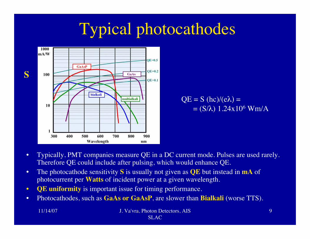
Typical photocathodes
• Typically, PMT companies measure QE in a DC current mode. Pulses are used rarely.Therefore QE could include after pulsing, which would enhance QE.
• The photocathode sensitivity S is usually not given as QE but instead in mA ofphotocurrent per Watts of incident power at a given wavelength.
• QE uniformity is important issue for timing performance.• Photocathodes, such as GaAs or GaAsP, are slower than Bialkali (worse TTS).
QE = S (hc)/(eλ) = = (S/λ) 1.24x10⁶ Wm/A
S

11/14/07 J. Va'vra, Photon Detectors, AISSLAC
10
Compilation of various Photocathodes
• In the past 20 years, there was a steady push to develop photocathodes operating in the visiblewavelength range. The main reasons: (a) The radiators are very chromatic in the UV region, (b)Materials are less transparent, expensive, (c) Mirrors are difficult to make, expensive, (d) The far UVregion is difficult to work in (cleanliness, outgasing pollution, etc).
• Benzene was used by HRS, TMAE by DELPHI, SLD, OMEGA, CERES, JETSET and CAPRICE;TEA by CLEO, CsI by ALICE, COMPASS, HADES; Bialkali by HERA-B, DIRC, HERMES, Belle,CELEX, Multi-alkali by LHC-b, and GaAsP, GaAs or Si will be pushed by new detectors.
• QE in TMAE, TEA and Benzene measured in the gas.
Compilation of data by J. Va‘vra, SLAC

11/14/07 J. Va'vra, Photon Detectors, AISSLAC
11
QE depends on the manufacturerCompilation of data by J. Va‘vra, SLAC
• We will see that moving towards the red wavelength range reduces the time spreadof the photoelectrons at the photocathode. However, the Cherenkov light yield issmaller for red wavelengths.
• For example, Photonis Multi-alkali photocathode, which I am not allowed to show, wouldyield half of photoelectrons compared to Burle Bialkali on MCP-PMT, all else equal.
Enhanced QE(Hamamatsu quote for H-8500at 420nm as of 2.8.2007)
11/14/07 J. Va'vra, Photon Detectors, AISSLAC
12
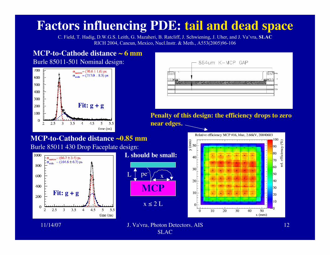
Factors influencing PDE: tail and dead spaceC. Field, T. Hadig, D.W.G.S. Leith, G. Mazaheri, B. Ratcliff, J. Schwiening, J. Uher, and J. Va’vra, SLAC
RICH 2004, Cancun, Mexico, Nucl.Instr. & Meth., A553(2005)96-106
MCP-to-Cathode distance ~ 6 mmBurle 85011-501 Nominal design:
Fit: g + g
Fit: g + g
Penalty of this design: the efficiency drops to zeronear edges.
MCP-to-Cathode distance ~0.85 mmBurle 85011 430 Drop Faceplate design:
MCPpe-L x
x ≤ 2 L
L should be small:
11/14/07 J. Va'vra, Photon Detectors, AISSLAC
13
Timing strategy(this is the hardest part of the problem)
11/14/07 J. Va'vra, Photon Detectors, AISSLAC
14
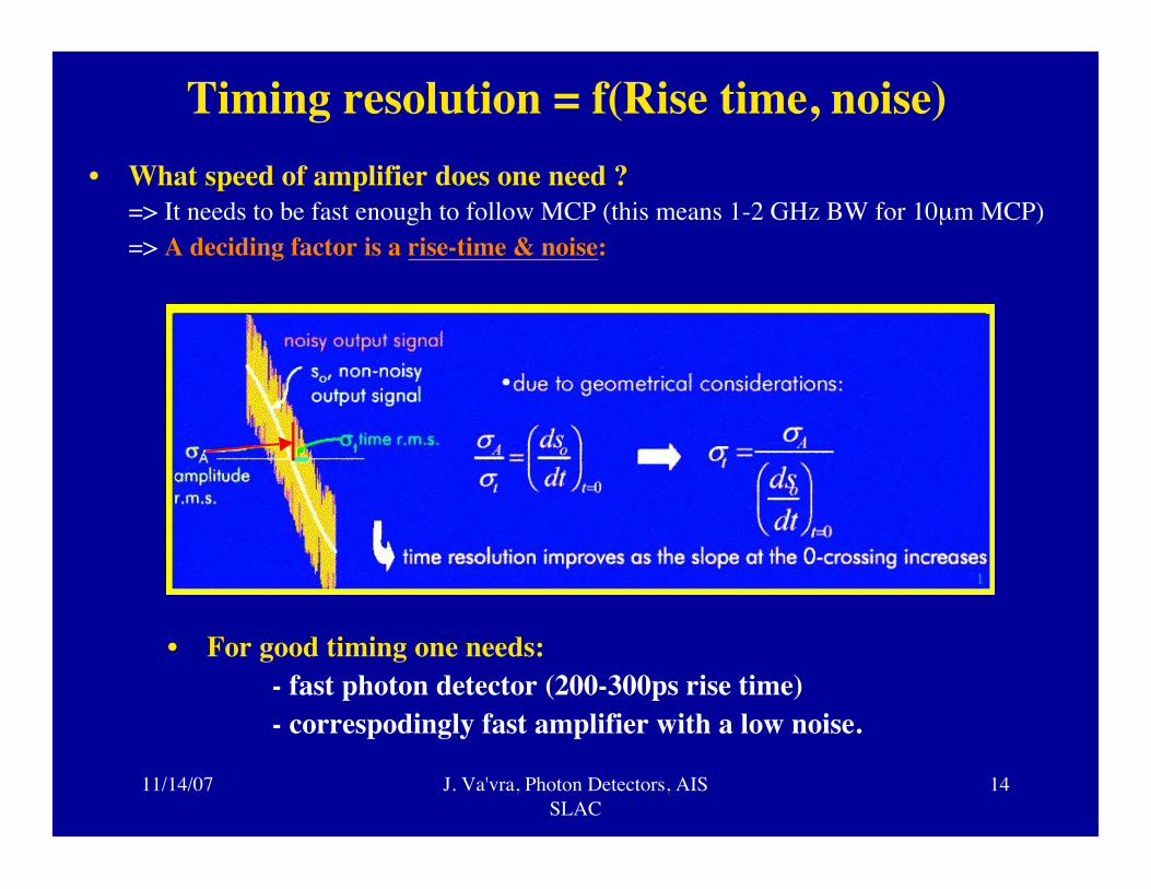
Timing resolution = f(Rise time, noise)• What speed of amplifier does one need ?
=> It needs to be fast enough to follow MCP (this means 1-2 GHz BW for 10µm MCP)=> A deciding factor is a rise-time & noise:
• For good timing one needs:- fast photon detector (200-300ps rise time)- correspodingly fast amplifier with a low noise.
11/14/07 J. Va'vra, Photon Detectors, AISSLAC
15
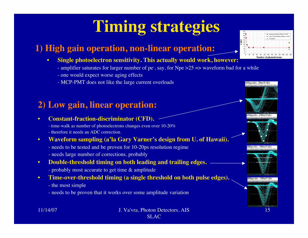
Timing strategies
• Constant-fraction-discriminator (CFD).- time-walk as number of photoelectrons changes even over 10-20%- therefore it needs an ADC correction.
• Waveform sampling (a’la Gary Varner’s design from U. of Hawaii).- needs to be tested and be proven for 10-20ps resolution regime- needs large number of corrections, probably
• Double-threshold timing on both leading and trailing edges.- probably most accurate to get time & amplitude
• Time-over-threshold timing (a single threshold on both pulse edges).- the most simple- needs to be proven that it works over some amplitude variation
1) High gain operation, non-linear operation:• Single photoelectron sensitivity. This actually would work, however:
- amplifier saturates for larger number of pe-, say, for Npe >25 => waveform bad for a while- one would expect worse aging effects- MCP-PMT does not like the large current overloads
2) Low gain, linear operation:. . ... ..
. ..
.

11/14/07 J. Va'vra, Photon Detectors, AISSLAC
16
• At a level of 5-10 ps, the time-walk needs to be corrected with ADC - for allmethods, including CFD method ! So, why to use a CFD discriminator at all ?
• Ortec 9327 Amp/CFD time-walk is the smallest, but still significant !
Zoom into a more likely range of variation in Npe:
Time-walk = f(Npe)Example of a CFD timing(zero-crossing point):

11/14/07 J. Va'vra, Photon Detectors, AISSLAC
17
Double threshold timing ?
• A double-threshold method does not lead to a single intersect point, probably due toa nonlinearity in the amplification process, if one accepts a large variation in Npe !It may work only over a small range of variation in Npe => need uniformity.
• Important point: (a) one should be linear, (b) Npe should not vary much.
• Burle/Photonis MCP-PMTs with 10 µm MCP holes operating at 2.80kV; no amplifier; red laser (635 nm).• Tektronix TDS 5104 scope with 1 GHz BW; trigger: PiLas trigger; thresholds 5 & 20 mV; scope: 200ps/div & 10 mV/div.

Some basic principles fordetector candidates for high
resolution timing
11/14/07 J. Va'vra, Photon Detectors, AISSLAC
19
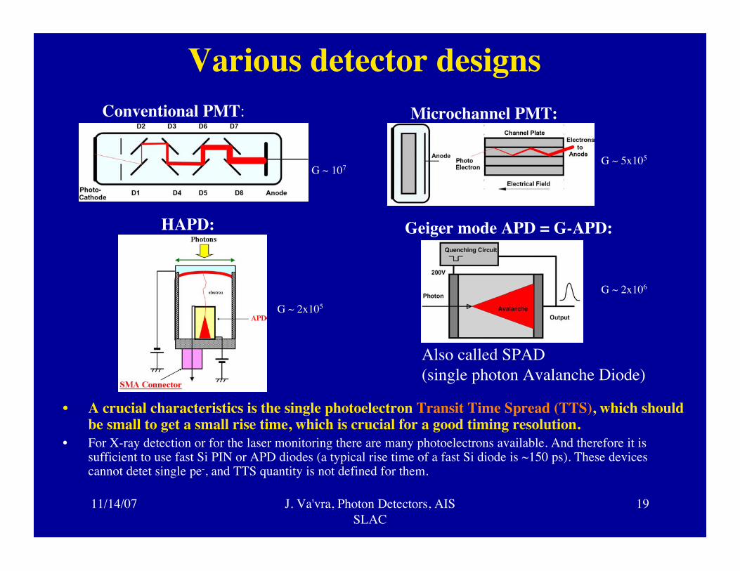
Various detector designsConventional PMT: Microchannel PMT:
Also called SPAD (single photon Avalanche Diode)
Geiger mode APD = G-APD:HAPD:
• A crucial characteristics is the single photoelectron Transit Time Spread (TTS), which shouldbe small to get a small rise time, which is crucial for a good timing resolution.
• For X-ray detection or for the laser monitoring there are many photoelectrons available. And therefore it issufficient to use fast Si PIN or APD diodes (a typical rise time of a fast Si diode is ~150 ps). These devicescannot detet single pe-, and TTS quantity is not defined for them.
G ~ 5x10⁵
G ~ 2x10⁶
G ~ 2x10⁵
G ~ 107

11/14/07 J. Va'vra, Photon Detectors, AISSLAC
20
Relative comparison of pulses
• MCP-PMT has lower gain, very narrow pulses, needs a fast amplifier, and needs afast ADC to know its charge.
• One consequence of the MCP speed is that one needs to have fast components(cables, splitters, terminatores, etc.), and many “usual” practices are not allowed.
Standard PMT: MaPMT: MCP-PMT:
~2 mV40 µA~400 ps~105PCP-PMT~ 5 mV100 µA~1.5 ns~106MaPMT16 mV0.32 mA~ 5 ns~107Standard
VSingle el. pulse(50Ω)ISingle el. pulsePulse FWHMPMT GainPMT
Isingle el. pule = Gxe/FWHM
11/14/07 J. Va'vra, Photon Detectors, AISSLAC
21
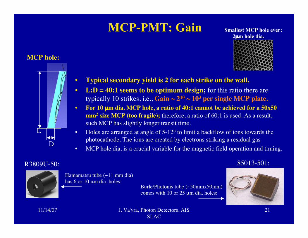
MCP-PMT: Gain
MCP hole:
• Typical secondary yield is 2 for each strike on the wall.• L:D = 40:1 seems to be optimum design; for this ratio there are
typically 10 strikes, i.e., Gain ~ 210 ~ 103 per single MCP plate.• For 10 µm dia. MCP hole, a ratio of 40:1 cannot be achieved for a 50x50
mm2 size MCP (too fragile); therefore, a ratio of 60:1 is used. As a result,such MCP has slightly longer transit time.
• Holes are arranged at angle of 5-12o to limit a backflow of ions towards thephotocathode. The ions are created by electrons striking a residual gas
• MCP hole dia. is a crucial variable for the magnetic field operation and timing.
L
D
Smallest MCP hole ever: 2µm hole dia.
Burle/Photonis tube (~50mmx50mm)comes with 10 or 25 µm dia. holes:
Hamamatsu tube (~11 mm dia)has 6 or 10 µm dia. holes:
R3809U-50: 85013-501:

11/14/07 J. Va'vra, Photon Detectors, AISSLAC
22
Single electron transit time spread - TTSStandard PMT: G-APD (=SPAD):
• Emission at the photocathode = f(λ).• Cathode-to-dynode transit (or 1-st MCP)• Multiplication process.• Emission at MCP exit towards anode.• Light source jitter
(usually one is trying to subtract this)• Timing jitter of subsequent electronics
(usually one is trying to subtract this)
Contributions to TTS:Standard PMT & MCP-PMT: G-APD:
• Different depth of photon conversion = f(λ).• Multiplication process.• Sensitivity to passive quenching circuit.• Light source jitter
(usually one is trying to subtract this)• Timing jitter of subsequent electronics
(usually one is trying to subtract this)
MCP-PMT:
σTTS(best) ~ 17 psσTTS(best) ~ 10-11 psσTTS(best) ~ 150 ps

11/14/07 J. Va'vra, Photon Detectors, AISSLAC
23
Example of a TTS measurement J.Va’vra, log book
5-m long fiber
Detector
Lens + collimator
Lens + collimator
Laser diode
Control unit
PiLas
1.5-meter longcable
Start
x & y stage +rotation
Detector
PiLas laser head:
62.5 µmFiber size
~ 30 psTTS light spread (FWHM)
635 nmWavelength
PiLasLaser diode source
SLAC testsParameter
Lens + collimator
5m-long fiber
Start
Calibration of a fast detector:
Ultra-fast Si Detector:(can use also a Streak camera)
11/14/07 J. Va'vra, Photon Detectors, AISSLAC
24
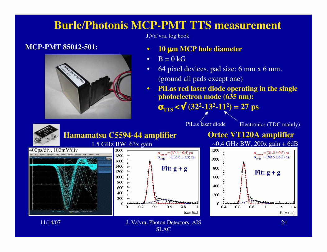
Burle/Photonis MCP-PMT TTS measurementJ.Va’vra, log book
• 10 µm MCP hole diameter• B = 0 kG• 64 pixel devices, pad size: 6 mm x 6 mm.
(ground all pads except one)• PiLas red laser diode operating in the single
photoelectron mode (635 nm):σTTS < √ (322-132-112) = 27 ps
Ortec VT120A amplifier ~0.4 GHz BW, 200x gain + 6dB
Fit: g + g
MCP-PMT 85012-501:
Fit: g + g
Hamamatsu C5594-44 amplifier 1.5 GHz BW, 63x gain
PiLas laser diode Electronics (TDC mainly)
11/14/07 J. Va'vra, Photon Detectors, AISSLAC
25
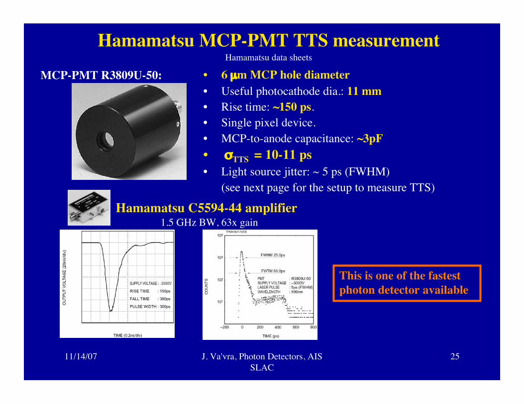
Hamamatsu MCP-PMT TTS measurementHamamatsu data sheets
• 6 µm MCP hole diameter• Useful photocathode dia.: 11 mm• Rise time: ~150 ps.• Single pixel device.• MCP-to-anode capacitance: ~3pF• σTTS = 10-11 ps• Light source jitter: ~ 5 ps (FWHM)
(see next page for the setup to measure TTS)
MCP-PMT R3809U-50:
Hamamatsu C5594-44 amplifier 1.5 GHz BW, 63x gain
This is one of the fastestphoton detector available

11/14/07 J. Va'vra, Photon Detectors, AISSLAC
26
Setup to measure a very small TTS of R3809U-50 tube(Hamamatsu Co.)
• Nd-YAG laser jitter: σ ~ 2.1 ps• Red wavelength: λ = 596 nm

Variables controlling theMCP rise time

11/14/07 J. Va'vra, Photon Detectors, AISSLAC
28
Rise time = f(MCP pore size)(Photek Ltd. & Burle/Photonis information)
Rise time =f(pore size) in MCP (Photek):18 GHz scope
0100200300400500600
0 5 10 15 20 25Pore size [microns]
Tran
sit ti
me
[ps] L:D = 40:1, V-MCP = 1000V
L:D = 60:1, V-MCP = 1500 V
Transit time in a MCP hole (from Burle):
Smaller pore size, smaller the transit time.
Smaller MCP pore size, faster rise time.Note: Cost to buy of ~18 GHz scope: ~$120k. Cost to rent: ~$5k/month.
11/14/07 J. Va'vra, Photon Detectors, AISSLAC
29
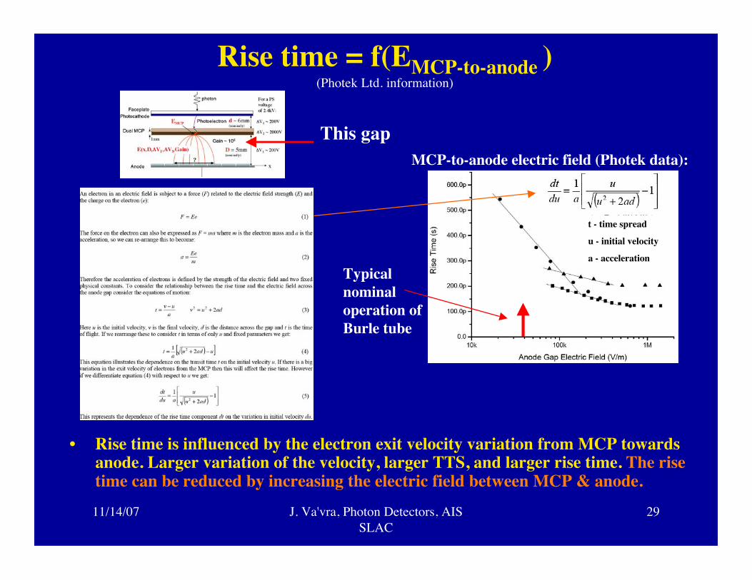
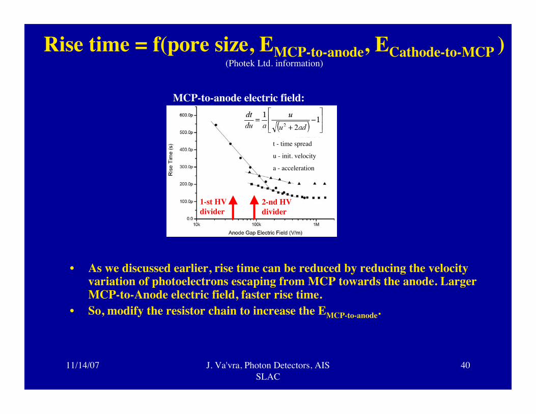
Rise time = f(EMCP-to-anode )(Photek Ltd. information)
• Rise time is influenced by the electron exit velocity variation from MCP towardsanode. Larger variation of the velocity, larger TTS, and larger rise time. The risetime can be reduced by increasing the electric field between MCP & anode.
MCP-to-anode electric field (Photek data):
t - time spread
u - initial velocity
a - acceleration
Typicalnominaloperation ofBurle tube
This gap

11/14/07 J. Va'vra, Photon Detectors, AISSLAC
30
Rise time = f(ECathode-to-MCP )(Photek Ltd. & Burle/Photonis information)
• Electron exit velocity variation from the cathode towards MCP affects the rise time also.However, it is a small effect for red wavelengths & Bialkali because:[635 nm <=> ~2 eV => dt/du|max ~ ((2-φ)/200 eV)*1000ps] ~ 0, for 200 Volts and Bialkaliphotocathode’s work fctn. φ ~1.5-2 eV. May be more significant for λ < 300 nm !!
Cathode-to-MCP voltage (Photek):
6µm MCP pore 5o hole angleλ = 635 nm
18 GHz scope
Cathode – MCP Transit Time (from Burle):
10
100
1000
10000
100 300 500 700 900 1100
MCP-to-Cathode voltage [V]
Tran
sit ti
me
[ps]
Cathode-to-MCP dist. = 6.1 mm
Cathode-to-MCP dist. = 0.86 mm
Increased voltage or decreased gap can reduce the transit time.
For red wavelength (635 nm), there is no variation of the rise time.
This gap
11/14/07 J. Va'vra, Photon Detectors, AISSLAC
31
An example of the detector possiblechoice for the TOF application
- Our effort- Nagoya U. effort

11/14/07 J. Va'vra, Photon Detectors, AISSLAC
32
Burle/Photonis MCP-PMT Burle/Photonis data
Faceplate
Anode & Pins
Indium Seal Dual MCP
Ceramic Insulators
A real device:
3 µAMaximum average total anode current
70 - 80% *Geometrical collection efficiency of the 1-st MCP
5.94 x 5.94 or ~1 x 1 [mm2]Pixel size (8x8 & 32x32 matrix)
4, 64, 256 or 1024Number of pixels
2x2, 8 x 8, 16x16 or 32 x 32Matrix of pixels
27 psσTTS - single electron transit time spread (for 10 µm dia. pores)
17 - 23% *PDE = Total fraction of “in time” photoelectrons detected (for Bi-alkali QE)
85 - 90% *Geometrical packing efficiency
~5 x 10⁵Total average gain @ -2.4kV & B = 0 kG
2Number of MCPs/PMT
28 - 32%Photocathode: Bi-alkali QE at 420nm
ValueParameter
* Higher number is for a future improvement

11/14/07 J. Va'vra, Photon Detectors, AISSLAC
33
A TOF counter prototype
• Burle/Photonis MCP-PMTs (85013-501) with 10 µm MCP holes.• Short together 4 pads to get a signal; all the rest of pads grounded.• A 10mm-long, 10mm dia, quartz radiator, Al-coating on cylinder sides.• Ortec 1GHz BW 9327Amp/CFD & TAC566 & 14 bit ADC114.• Calculation: 10mm long quartz radiator & a window should give Npe ~ 50 pe/track.• Laser diode light can be easily adjusted to provide Npe ~ 1- 200 pe.• The laser spot size: ~1mm dia.; beam spot size typically σ ~1-2mm
Four pads connected via equal-time traces:
Quartz radiator
11/14/07 J. Va'vra, Photon Detectors, AISSLAC
34
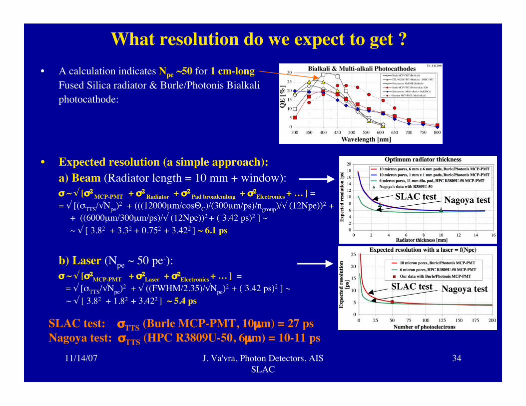
What resolution do we expect to get ?• A calculation indicates Npe ~50 for 1 cm-long
Fused Silica radiator & Burle/Photonis Bialkaliphotocathode:
• Expected resolution (a simple approach):a) Beam (Radiator length = 10 mm + window):σ ~ √ [σ2
MCP-PMT + σ2 Radiator + σ2
Pad broadenibng + σ2Electronics + … ] =
= √ [(σTTS/√Npe)2 + (((12000µm/cosΘC)/(300µm/ps)/ngroup)/√ (12Npe))2 + + ((6000µm/300µm/ps)/√ (12Npe))2 + ( 3.42 ps)2 ] ~ ~ √ [ 3.82 + 3.32 + 0.752 + 3.422 ] ~ 6.1 ps
b) Laser (Npe ~ 50 pe-):σ ~ √ [σ2
MCP-PMT + σ2Laser + σ2
Electronics + … ] = = √ [σTTS/√Npe)2 + √ ((FWHM/2.35)/√Npe)2 + ( 3.42 ps)2 ] ~
~ √ [ 3.82 + 1.82 + 3.422 ] ~ 5.4 ps
SLAC test: σTTS (Burle MCP-PMT, 10µm) = 27 psNagoya test: σTTS (HPC R3809U-50, 6µm) = 10-11 ps
SLAC test Nagoya test
SLAC test Nagoya test

11/14/07 J. Va'vra, Photon Detectors, AISSLAC
35
Setup with two MCP-PMTs and a fiber splitter
START
STOP
ADC 114
TAC 566
σ MCP-PMT
Ortec 9327 Amp/CFD
Ortec 9327 Amp/CFD
Control unit
PiLas635 nm
Laser diode
Fiber splitter MCP_stop
MCP_start
Npe ~ 502.33 kV400 ps/div10 mV/div

11/14/07 J. Va'vra, Photon Detectors, AISSLAC
36
Calibration of the electronics
Pulser
START
STOP
ADC 114
TAC 566
σ MCP-PMT
σ = √ [2 σ2MCP-PMT + (σ2
Pulser+TAC_ADC+Amp/CFD - σ2Pulser)]
+ Systematic effects (much smaller when the PiLas source eliminated)
σ Pulser + TAC_ADC + Amp/CFD ~ 3.42 ps
Ortec 9327 Amp/CFD
Ortec 9327 Amp/CFD
Control unit
PiLas635 nm
Laser diode
Fiber splitter
MCP_stop
MCP_start
σ ~ 3.42 ps
20dB att.
20dB att.
• The best electronics performance to my knowledge.

11/14/07 J. Va'vra, Photon Detectors, AISSLAC
37
A final result with two TOF counters in tandem
• Two Burle/Photonis MCP-PMTs with 10 µm MCP holes operating at 2.27 & 1.88 kV.• Ortec 9327Amp/CFD (two) with a -10mV threshold and a walk threshold of +5mV & TAC566 & 14 bit ADC114
σsingle detector ~ (1/√2) σ double detector ~ 7.2 psσ ~ 10.2 ps
Two detector resolution (Npe ~50 pe):
Each detector has Npe ~ 50 pe-:
Running conditions:1) Low MCP gain operation (<105)2) Linear operation3) CFD discriminator4) No additional ADC correction
ADC [counts]
11/14/07 J. Va'vra, Photon Detectors, AISSLAC
38
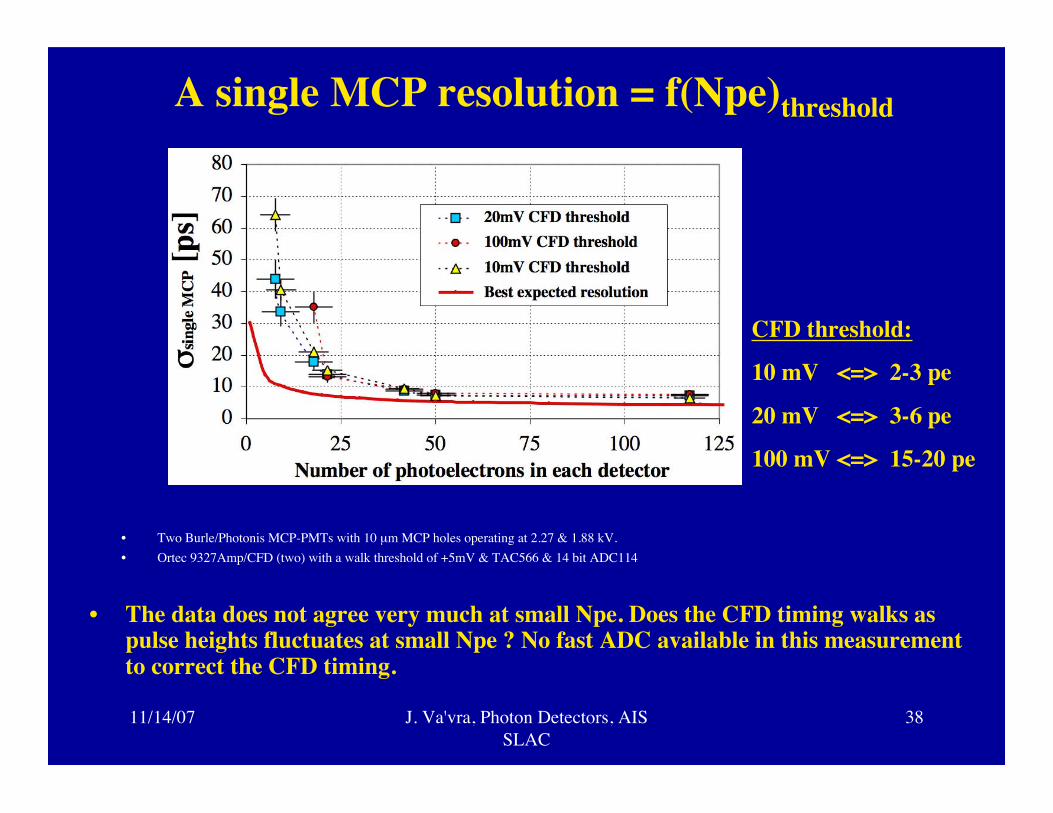
A single MCP resolution = f(Npe)threshold
• The data does not agree very much at small Npe. Does the CFD timing walks aspulse heights fluctuates at small Npe ? No fast ADC available in this measurementto correct the CFD timing.
CFD threshold:
10 mV <=> 2-3 pe
20 mV <=> 3-6 pe
100 mV <=> 15-20 pe
• Two Burle/Photonis MCP-PMTs with 10 µm MCP holes operating at 2.27 & 1.88 kV.• Ortec 9327Amp/CFD (two) with a walk threshold of +5mV & TAC566 & 14 bit ADC114

11/14/07 J. Va'vra, Photon Detectors, AISSLAC
39
Can we improve it further ?
11/14/07 J. Va'vra, Photon Detectors, AISSLAC
40
Rise time = f(pore size, EMCP-to-anode, ECathode-to-MCP )(Photek Ltd. information)
• As we discussed earlier, rise time can be reduced by reducing the velocityvariation of photoelectrons escaping from MCP towards the anode. LargerMCP-to-Anode electric field, faster rise time.
• So, modify the resistor chain to increase the EMCP-to-anode.
MCP-to-anode electric field:
1-st HV divider
2-nd HV divider
t - time spread
u - init. velocity
a - acceleration
11/14/07 J. Va'vra, Photon Detectors, AISSLAC
41
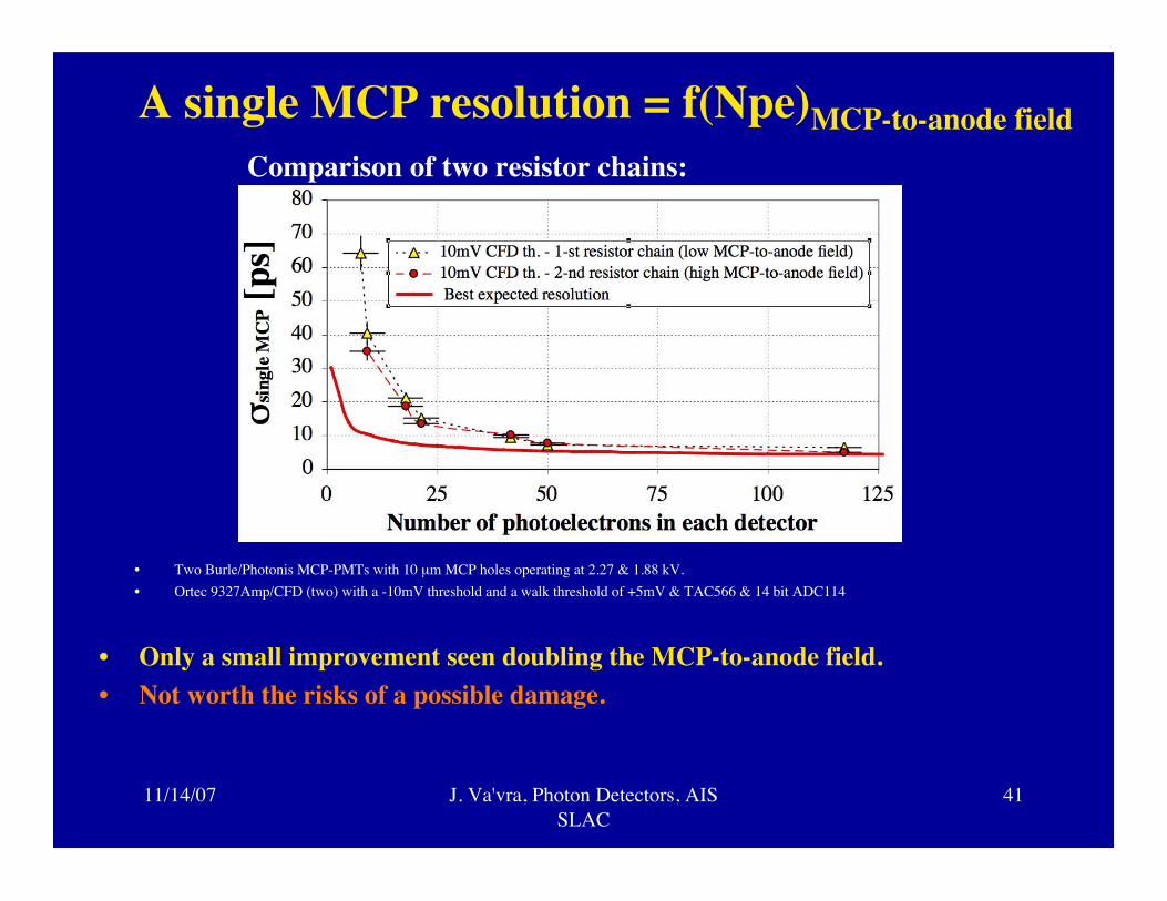
A single MCP resolution = f(Npe)MCP-to-anode field
• Only a small improvement seen doubling the MCP-to-anode field.• Not worth the risks of a possible damage.
Comparison of two resistor chains:
• Two Burle/Photonis MCP-PMTs with 10 µm MCP holes operating at 2.27 & 1.88 kV.• Ortec 9327Amp/CFD (two) with a -10mV threshold and a walk threshold of +5mV & TAC566 & 14 bit ADC114

11/14/07 J. Va'vra, Photon Detectors, AISSLAC
42
The best result with two TOF counters in tandem
• Two Burle/Photonis MCP-PMTs with 10 µm MCP holes operating at 2.85 & 2.43 kV.• Ortec 9327Amp/CFD (two) with a walk th. of +5mV & TAC566 & 14 bit ADC11
σsingle detector ~ (1/√2) σ double detector ~ 5.0 ps
Two detector resolution (resistor chain #2):
Contribution of the MCP-PMT itself to the above single detector resolution:
σMCP-PMT < √1/2 { σ2 - [σ2
Pulser+TAC_ADC+Amp/CFD - σ2Pulser ]} < 4.5 ps
< 2 ps (manufacturer)3.42 ps7.0 ps
Each detector has Npe ~ 115-120 pe-:
σ ~ 7.0 ps
Running conditions:1) Low MCP gain operation (<105)2) Linear operation3) CFD discriminator4) No additional ADC correction
11/14/07 J. Va'vra, Photon Detectors, AISSLAC
43
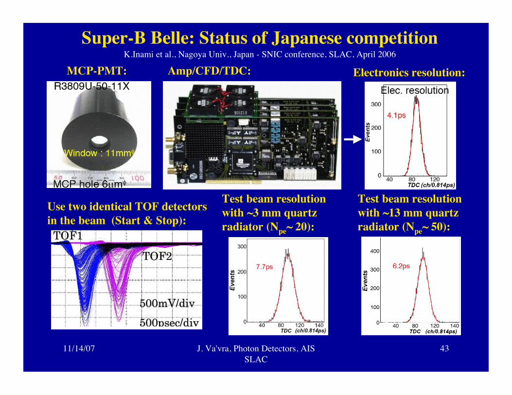
Super-B Belle: Status of Japanese competitionK.Inami et al., Nagoya Univ., Japan - SNIC conference, SLAC, April 2006
Electronics resolution:
Test beam resolution with ~13 mm quartz radiator (Npe~ 50):
Use two identical TOF detectorsin the beam (Start & Stop):
Amp/CFD/TDC:MCP-PMT:
Test beam resolution with ~3 mm quartz radiator (Npe~ 20):
Other competing fast detectors
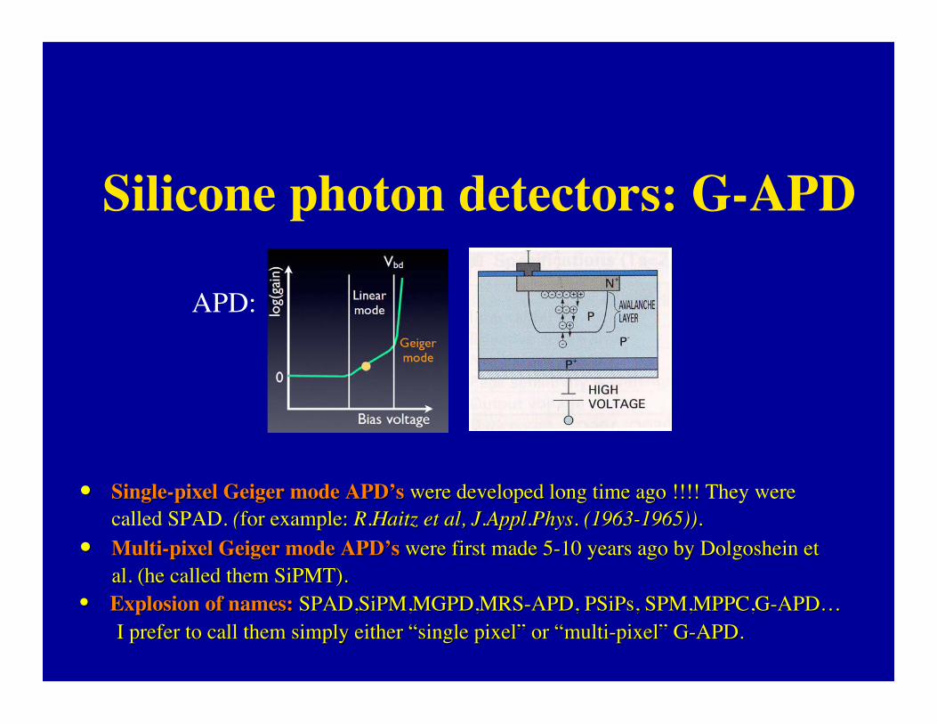
Silicone photon detectors: G-APD
•• Single-Single-pixel Geiger mode APDpixel Geiger mode APD’’ss were developed long time were developed long time agoago !!!! !!!! They were called SPAD. ( (for example: for example: R.Haitz et al, J.Appl.Phys. (1963-1965)).R.Haitz et al, J.Appl.Phys. (1963-1965)).•• Multi-pixel Geiger mode APDMulti-pixel Geiger mode APD’’ss were first made were first made 5-10 years ago 5-10 years ago by Dolgoshein etby Dolgoshein et al. al. (he called them SiPMT).(he called them SiPMT).•• Explosion of names: Explosion of names: SPAD,SiPM SPAD,SiPM,MGPD,MRS-APD,MGPD,MRS-APD, , PSiPsPSiPs, , SPM,MPPCSPM,MPPC,G-APD,G-APD…… I prefer to call them simply I prefer to call them simply either either ““single pixelsingle pixel”” or or ““multi-pixelmulti-pixel”” G-APD. G-APD.
APD:
11/14/07 J. Va'vra, Photon Detectors, AISSLAC
46
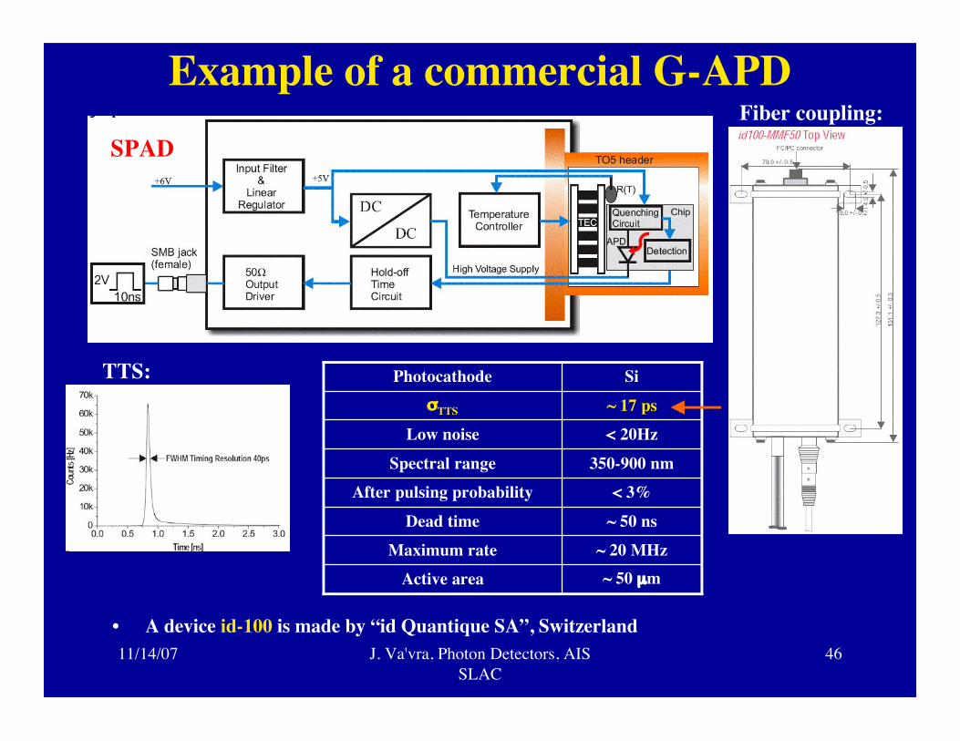
Example of a commercial G-APD
• A device id-100 is made by “id Quantique SA”, Switzerland
TTS:
Fiber coupling:SPAD
~ 50 µmActive area~ 20 MHzMaximum rate
~ 50 nsDead time
< 3%After pulsing probability350-900 nmSpectral range
< 20HzLow noise~ 17 psσTTS
SiPhotocathode
11/14/07 J. Va'vra, Photon Detectors, AISSLAC
47
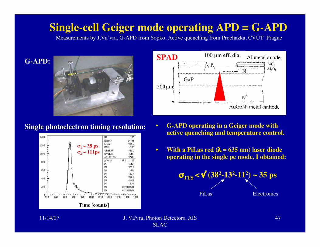
Single-cell Geiger mode operating APD = G-APD Measurements by J.Va’vra, G-APD from Sopko, Active quenching from Prochazka, CVUT Prague
• G-APD operating in a Geiger mode withactive quenching and temperature control.
• With a PiLas red (λ = 635 nm) laser diodeoperating in the single pe mode, I obtained:
σTTS < √ (382-132-112) ~ 35 ps
Single photoelectron timing resolution:
G-APD:100 µm eff. dia.
GaP
PiLas Electronics
SPAD
11/14/07 J. Va'vra, Photon Detectors, AISSLAC
48
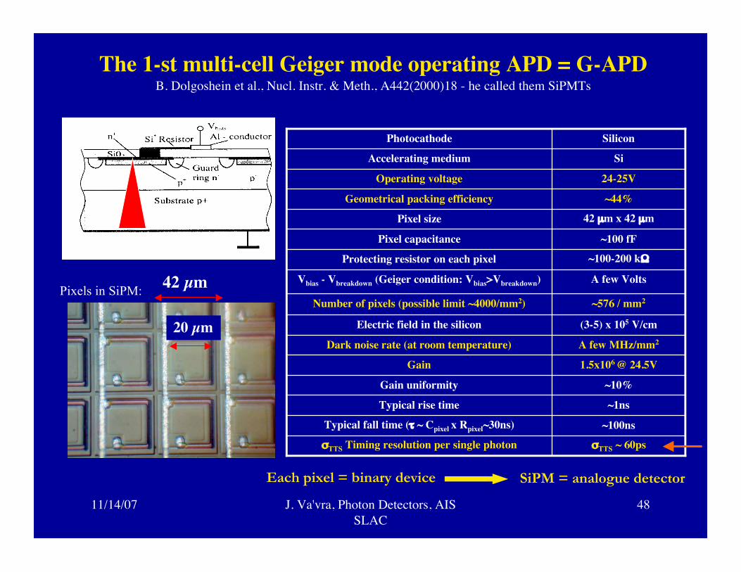
The 1-st multi-cell Geiger mode operating APD = G-APDB. Dolgoshein et al., Nucl. Instr. & Meth., A442(2000)18 - he called them SiPMTs
σTTS ~ 60psσTTS Timing resolution per single photon
~100nsTypical fall time (τ ~ Cpixel x Rpixel~30ns)
~1nsTypical rise time
~10%Gain uniformity
1.5x10⁶ @ 24.5VGain
A few MHz/mm2Dark noise rate (at room temperature)
(3-5) x 105 V/cmElectric field in the silicon
~576 / mm2Number of pixels (possible limit ~4000/mm2)
A few VoltsVbias - Vbreakdown (Geiger condition: Vbias>Vbreakdown)
~100-200 kΩProtecting resistor on each pixel
~100 fFPixel capacitance
42 µm x 42 µmPixel size
~44%Geometrical packing efficiency
24-25VOperating voltage
SiAccelerating medium
SiliconPhotocathode
42 µm
20 µm
Pixels in SiPM:
Each pixel = binary device SiPM = analogue detector

11/14/07 J. Va'vra, Photon Detectors, AISSLAC
49
How does a multi-pixel G-APD compareto MCP-PMT for a TOF application ?
• MCP-PMTs are winners for timing, although a resolution of σG-APD ~ 12psfor 1 cm thick quartz radiator (~50 pe) is not bad.
A simple calculation, assuming σTTS (G-APD)~ 80 ps:

11/14/07 J. Va'vra, Photon Detectors, AISSLAC
50
HAPD
A combination of vacuum tube and APD
11/14/07 J. Va'vra, Photon Detectors, AISSLAC
51
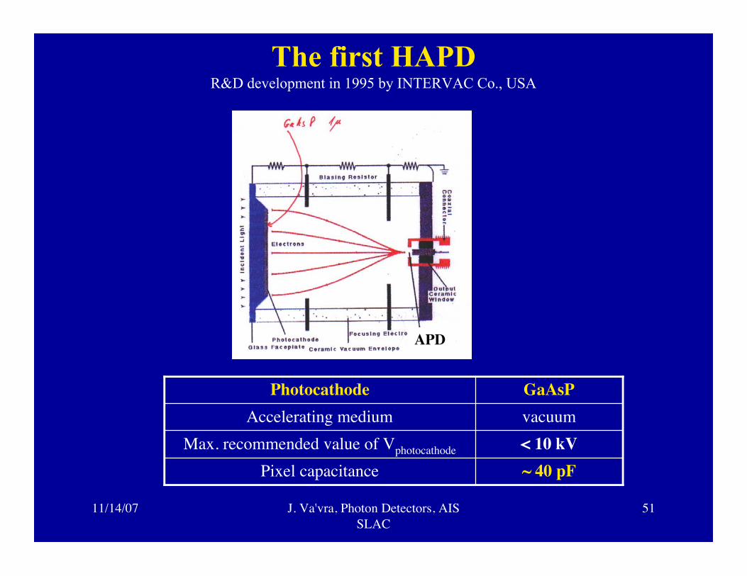
The first HAPDR&D development in 1995 by INTERVAC Co., USA
~ 40 pFPixel capacitance< 10 kVMax. recommended value of Vphotocathode
vacuumAccelerating mediumGaAsPPhotocathode
APD
11/14/07 J. Va'vra, Photon Detectors, AISSLAC
52
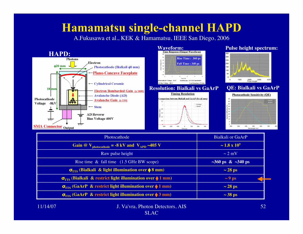
Hamamatsu single-channel HAPDA.Fukusawa et al., KEK & Hamamatsu, IEEE San Diego, 2006
~ 28 psσTTS (Bialkali & light illumination over φ 8 mm)
~ 9 psσTTS (Bialkali & restrict light illumination over φ 1 mm)
~ 28 psσTTS (GaArP & restrict light illumination over φ 1 mm)
~ 38 psσTTS (GaArP & restrict light illumination over φ 3 mm)
~360 ps & ~340 psRise time & fall time (1.5 GHz BW scope)
~ 2 mVRaw pulse height
~ 1.8 x 10⁵Gain @ Vphotocathode = -8 kV and VAPD ~405 V
Bialkali or GaArPPhotocathode
HAPD:Pulse height spectrum:Waveform:
Resolution: Bialkali vs GaArP QE: Bialkali vs GaArP

11/14/07 J. Va'vra, Photon Detectors, AISSLAC
53
HPD with Multi-pixel Avalanche DiodeHPD with Multi-pixel Avalanche DiodeJ. Haba, S. Iwata, M. Sakuda, F. Takasaki, M. Tanaka, T. Tsuboyama, Y. Yamada (KEK), T. Sumiyoshi (Tokyo
Metropolitan Univ.), T. Iijima (Nagoya Univ.), A. Fukasawa (Hamamatsu Photonics K.K.)
• Proximity focusing design=> can work in magnetic field
• Relatively small gain so far.
HAPD with 8x8 APD array:
8 x 8APD pixel matrix
2 x 2 mm2Area per pixel
~0.12 mmLow gain region between pixels
~ 90 psTransit time spread σTTS
~5 x 10⁴Total Gain (design)
~ 50Total APD gain @ 400 V
~ 2000Total HPD gain @ -8kV
16 x 16 mm2Sensitive area
~400 VoltsMax. APD diode bias voltage VAPD
~ 9 kVMax. value of Vphotocathode
Multi-alkaliPhotocathode
Timing resolution:
Back-illuminated APD array => more uniformity

11/14/07 J. Va'vra, Photon Detectors, AISSLAC
54
Hamamatsu HAPD for MAGIC experimentBased on the initial development of R7110U-01MOD tube - initiated by E. Lorenz,
Present work: J.Ninkovic, M. Hayashida, J. Hose, C. Hsu, R. Mirozyan, M. Teshima.MPI/Hamamatsu joint development for MAGIC experiment
24 pFPixel capacitance
~ 1600Total HPD gain @ -8kV
~2.1 nsPulse width
~1.9 nsFall time
~0.8 nsRise time
~8 x 10⁴Total gain (APD gain alone is ~30x)
~ 50Total APD gain @ 400 V
18 mm dia.Sensitive area
~400 VoltsAPD diode bias voltage VAPD
-8 kVMax. value of Vphotocathode
250 < λ < 700Bandwidth [nm]
GaAsPPhotocathode
Pulse height spectrum:
The MAGIC telescope:
Very fast pulses thanks to small capacitance:
HAPD:

11/14/07 J. Va'vra, Photon Detectors, AISSLAC
55
Summary of best resultsSummary of best resultsBest timing results in the field of photon detectors:a) Laser:
− ΜCP-PMT R3809U-50 (6µm holes): σ TTS ~ 10-11 ps for Npe ~ 1(Hamamatsu measurement).
− ΗAPD (restrict light to 1 mm dia.): σ TTS ~ 9 ps for Npe ~ 1(KEK group with Hamamatsu tube).
− ΜCP-PMT 85013-501(10µm holes): σ single MCP ~ 5.0 ps for Npe ~ 50,(my measurements with Burle/Photonis tube).
b) Particle beam:− ΜCP-PMT R3809U-50-11X (6µm holes): σ TTS ~ 6.2 ps for Npe ~ 50
(Nagoya Univ. group with Hamamatsu tube).
c) Best electronics bench performance:− Εlectronics contribution: σ Total_electronics ~ 3.4 ps
(my measurement with Ortec 1 GHz BW Amp/CFD 9327, TAC566, 14 bitADC114, and a fast pulser).
11/14/07 J. Va'vra, Photon Detectors, AISSLAC
56
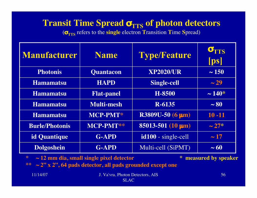
Transit Time Spread σTTS of photon detectors(σTTS refers to the single electron Transition Time Spread)
~ 29Single-cellHAPDHamamatsu
10 -11R3809U-50 (6 µm)MCP-PMT*Hamamatsu
~ 17id100 - single-cellG-APDid Quantique~ 60Multi-cell (SiPMT)G-APDDolgoshein
~ 27*85013-501 (10 µm)MCP-PMT**Burle/Photonis
~ 80R-6135Multi-meshHamamatsu~ 140*H-8500Flat-panelHamamatsu
~ 150XP2020/URQuantaconPhotonis
σTTS[ps]Type/FeatureNameManufacturer
* ~ 12 mm dia, small single pixel detector** ~ 2” x 2”, 64 pads detector, all pads grounded except one
* measured by speaker

11/14/07 J. Va'vra, Photon Detectors, AISSLAC
57
Towards a final TOF detectordesign

11/14/07 J. Va'vra, Photon Detectors, AISSLAC
58
Towards a better MCP-PMT design for timing
• Starting parameters, which Burle/Photonis is willing to try next:- 5 mm quartz window & radiator => ~ 25 pe-
- 0.07” (~1.8mm) cathode-to-MCP distance (allows a placement of a getter).- 0.02” (~0.5mm) MCP-to-anode distance.- 64 pads, 6x6 mm initially, combine 4 into one just like we did so far. This would create 16 macro-pixels.
• Electronics:- One threshold on leading edge and one on the trailing edge of a pulse.
MCP-PMT:

This is end
Let’s hope that we will not have wait another ~35 yearsbefore a high resolution timing will become reality

11/14/07 J. Va'vra, Photon Detectors, AISSLAC
60
Backup slides

11/14/07 J. Va'vra, Photon Detectors, AISSLAC
61
Bad effects

11/14/07 J. Va'vra, Photon Detectors, AISSLAC
62
Cross-talk and coherent oscillations inBurle/Photonis MCP-PMTs
• MCP avalanche is a very fast phenomenon. It can excite a resonance in a cableharness or cause reflections. One needs to do a coupling to the anode with a care.Preferably electronics should be on the tube, and one has to work closely with thecompany to fix this.
• For comparison, MaPMT H-8500 does not have this problem.
A.Brandt’s MCP-PMT with his cable harness(tests related to the LHC FP420 experiment):
When a large number of pe arrives at MCP, cross-talk adds coherently (FDIRC prototype):
All pixels shows this All pixels shows this
11/14/07 J. Va'vra, Photon Detectors, AISSLAC
63
Systematic effects
11/14/07 J. Va'vra, Photon Detectors, AISSLAC
64
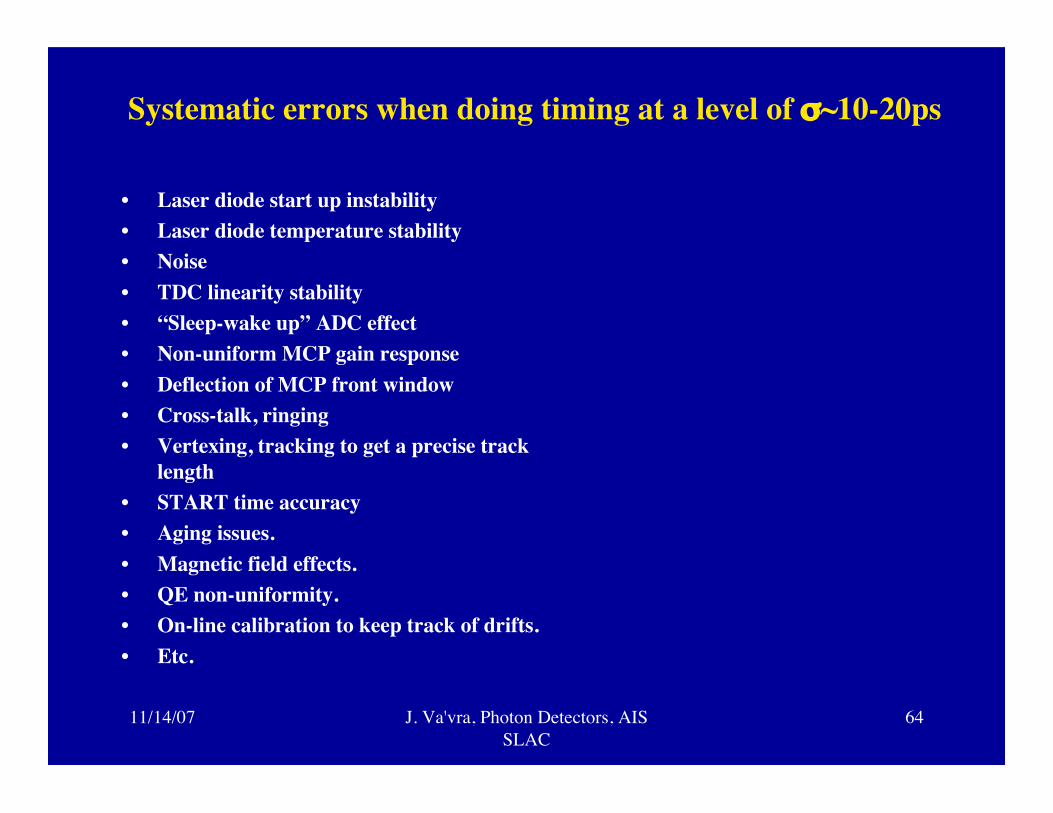
Systematic errors when doing timing at a level of σ~10-20ps
• Laser diode start up instability• Laser diode temperature stability• Noise• TDC linearity stability• “Sleep-wake up” ADC effect• Non-uniform MCP gain response• Deflection of MCP front window• Cross-talk, ringing• Vertexing, tracking to get a precise track
length• START time accuracy• Aging issues.• Magnetic field effects.• QE non-uniformity.• On-line calibration to keep track of drifts.• Etc.

11/14/07 J. Va'vra, Photon Detectors, AISSLAC
65
Magnetic field effects

11/14/07 J. Va'vra, Photon Detectors, AISSLAC
66
MCP gain reduction in a magnetic field
• Gain in MCP: G ~ e(A*MCP thickness/MCP dia) - drops in a magnetic field.• 25µm dia. holes are too large. One needs to reduce their size to ~6-10µm dia.,
to operate at 15kG.
Russian MCP-PMT:Barnyakov et al., Novosibirsk, Russia, The 10th Pisa meeting, La Biodola, Italy, 2006
Burle MCP-PMT:M.Akatsu et al., Nagoya, Japan
8 µm

11/14/07 J. Va'vra, Photon Detectors, AISSLAC
67
Aging issues

11/14/07 J. Va'vra, Photon Detectors, AISSLAC
68
Aging rate of MCP-PMTI.Adachi, et al., Nagoya University, SuperB workshop at SLAC
• The protective Al2O3 layer blocks the positive ions backflow to cathode.• Nagoya group predicts ~13 years of lifetime at Super B-factory.• However, there is a price: a 40% reduction of the photoelectron transmission.• Japanese group concluded that the Russian protective film does not work as well.• Russian results indicate that the blockage of positive ions with 3 MCPs seems to
be as effective as with a protective Al2O3 layer, up to a rate of ~108 pe/sec. Theydo not show an equivalent integrated charge dose as the Nagoya people show.
• It is hopeful, but more studies are needed.
A. Barnyakov et al., Novosibirsk, Russia
The 10th Pisa meeting, La Biodola, Italy, 2006
Three MCP solution:Protective Al2O3 film:

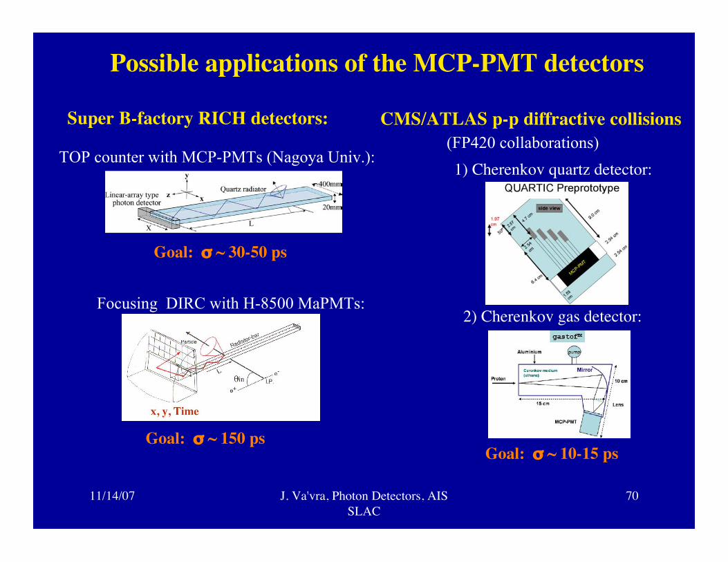
Applications for fast timing
11/14/07 J. Va'vra, Photon Detectors, AISSLAC
70
2) Cherenkov gas detector:
1) Cherenkov quartz detector:
Goal: σ ~ 10-15 ps
CMS/ATLAS p-p diffractive collisionsSuper B-factory RICH detectors:
TOP counter with MCP-PMTs (Nagoya Univ.):
Focusing DIRC with H-8500 MaPMTs:
Possible applications of the MCP-PMT detectors
(FP420 collaborations)
Goal: σ ~ 30-50 ps
Goal: σ ~ 150 ps
11/14/07 J. Va'vra, Photon Detectors, AISSLAC
71
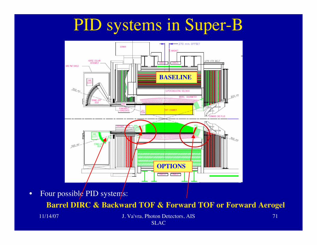
PID systems in Super-B
• Four possible PID systems: Barrel DIRC & Backward TOF & Forward TOF or Forward Aerogel
BASELINE
OPTIONS

11/14/07 J. Va'vra, Photon Detectors, AISSLAC
72
Timing at a level of σ ~15ps can startcompeting with the RICH techniques
• The PID performance of a forward TOF system with σ ~15-20ps isequivalent to the PID performance of BaBar DIRC.
Example of variousSuper-BfactoryPID designs:
Calculation done for Flight Path Length = 2m
11/14/07 J. Va'vra, Photon Detectors, AISSLAC
73
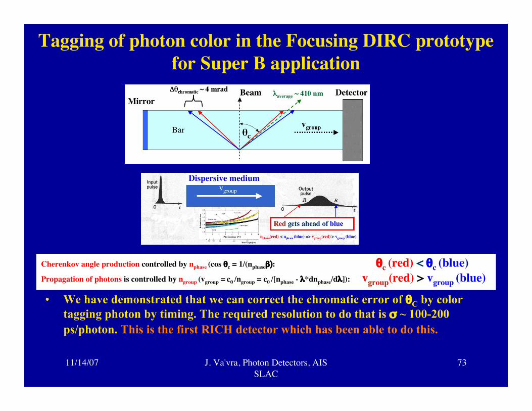
Tagging of photon color in the Focusing DIRC prototypefor Super B application
• We have demonstrated that we can correct the chromatic error of θC by colortagging photon by timing. The required resolution to do that is σ ~ 100-200ps/photon. This is the first RICH detector which has been able to do this.
Cherenkov angle production controlled by nphase (cos θc = 1/(nphaseβ): θc (red) < θc (blue)Propagation of photons is controlled by ngroup (vgroup = c0 /ngroup = c0 /[nphase - λ*dnphase/dλ]): vgroup(red) > vgroup (blue)
11/14/07 J. Va'vra, Photon Detectors, AISSLAC
74
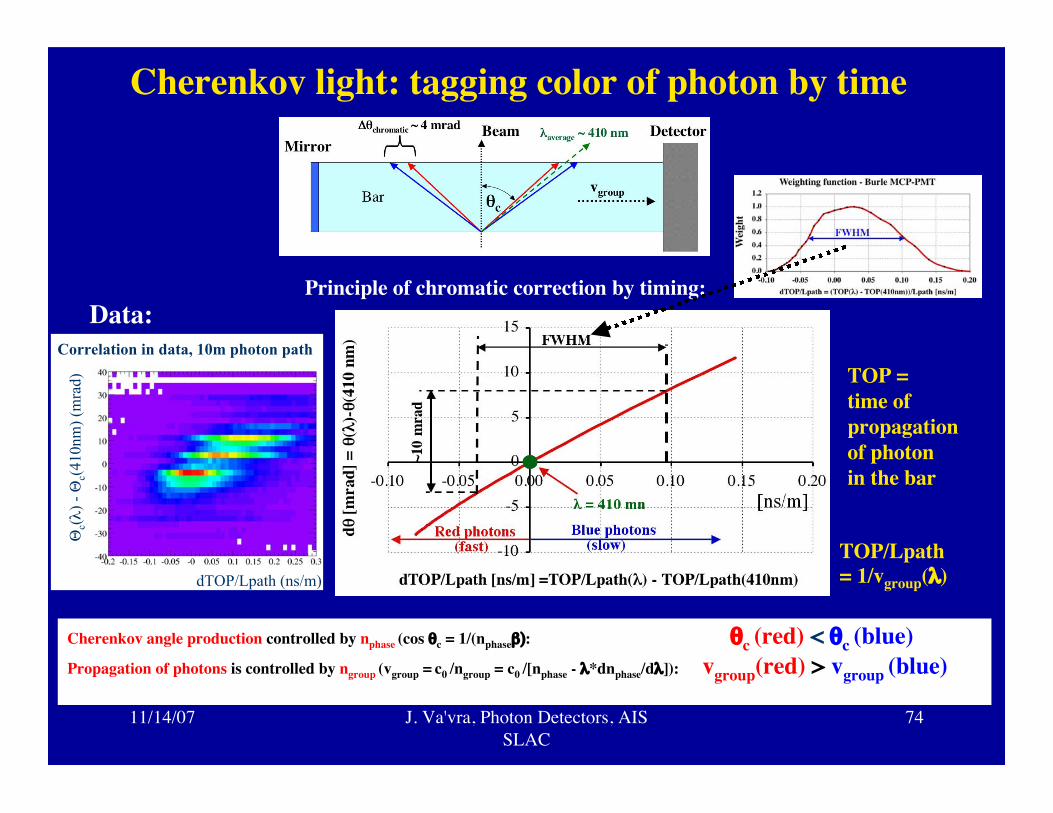
Cherenkov light: tagging color of photon by time
Cherenkov angle production controlled by nphase (cos θc = 1/(nphaseβ): θc (red) < θc (blue)Propagation of photons is controlled by ngroup (vgroup = c0 /ngroup = c0 /[nphase - λ*dnphase/dλ]): vgroup(red) > vgroup (blue)
Principle of chromatic correction by timing:
TOP = time ofpropagationof photonin the bar
TOP/Lpath = 1/vgroup(λ)dTOP/Lpath (ns/m)
Θc(λ
) - Θ
c(410
nm) (
mra
d )
Correlation in data, 10m photon path
Data:
11/14/07 J. Va'vra, Photon Detectors, AISSLAC
75
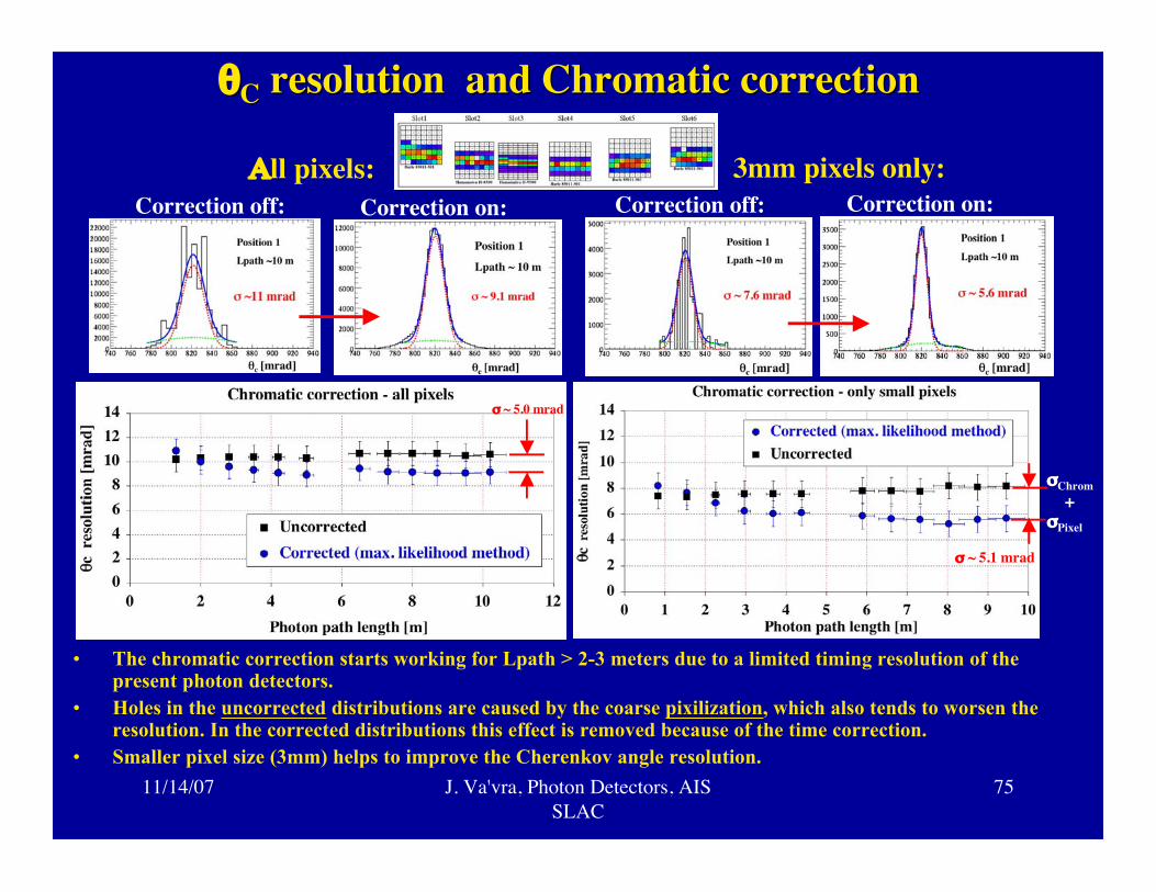
θθCC resolution and Chromatic correction resolution and Chromatic correction
Αll pixels: 3mm pixels only:
• The chromatic correction starts working for Lpath > 2-3 meters due to a limited timing resolution of thepresent photon detectors.
• Holes in the uncorrected distributions are caused by the coarse pixilization, which also tends to worsen theresolution. In the corrected distributions this effect is removed because of the time correction.
• Smaller pixel size (3mm) helps to improve the Cherenkov angle resolution.
Correction off: Correction off:Correction on: Correction on:
σ ~ 5.0 mrad
σ ~ 5.1 mrad
σChrom +σPixel
11/14/07 J. Va'vra, Photon Detectors, AISSLAC
76
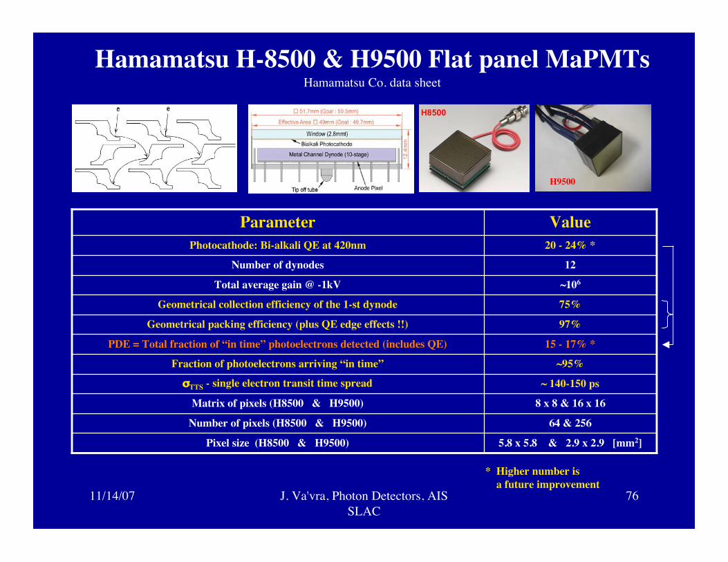
Hamamatsu H-8500 & H9500 Flat panel MaPMTsHamamatsu Co. data sheet
~95%Fraction of photoelectrons arriving “in time”
20 - 24% *Photocathode: Bi-alkali QE at 420nm
75%Geometrical collection efficiency of the 1-st dynode
5.8 x 5.8 & 2.9 x 2.9 [mm2]Pixel size (H8500 & H9500)
64 & 256Number of pixels (H8500 & H9500)
8 x 8 & 16 x 16Matrix of pixels (H8500 & H9500)
~ 140-150 psσTTS - single electron transit time spread
15 - 17% *PDE = Total fraction of “in time” photoelectrons detected (includes QE)
97%Geometrical packing efficiency (plus QE edge effects !!)
~106Total average gain @ -1kV
12Number of dynodes
ValueParameter
H9500
* Higher number is a future improvement

11/14/07 J. Va'vra, Photon Detectors, AISSLAC
77
Hamamatsu MaPMT
• MaPMT has much smaller tailcompared to MCP-PMTs.
• The Hamamatsu MaPMTuniformity is ~1:2.5, compared toBurle’s MCP-PMT uniformity of~1:1.5.
• Hamamatsu Flat Panel MaPMTrelative efficiency is 50-70% ofthe Photonis XP 2262B PMT at430nm. The efficiency drops to30-50% around the edges.
• Clearly see the details of the dynodeelectrode structure. Spatialresolution of the system is less than150 µm, for a step size of 25µm.
Flat Panel H8500 PMT:
C. Field, T. Hadig, D.W.G.S. Leith, G. Mazaheri, B. Ratcliff, J. Schwiening, J. Uher, and J. Va’vra, RICH 2004, Cancun, Mexico, Nucl.Instr. & Meth., A553(2005)96-106
430nm:
Micro-structure of the dynode electrodes: