Embed Size (px)
Citation preview

High-resolution light field prints by nanoscale 3D printing Authors: John You En Chan 1, Qifeng Ruan 1 *, Menghua Jiang 2, Hongtao Wang 1,
Hao Wang 1, Wang Zhang 1, Cheng-Wei Qiu 2, Joel K.W. Yang 1,3 *
1 Engineering Product Development, Singapore University of Technology and
Design, Singapore 487372. 2 Department of Electrical and Computer Engineering, National University of
Singapore, Singapore 117583. 3 Institute of Materials Research and Engineering, Singapore 138634.
* To whom correspondence should be addressed. Email: [email protected];

Abstract A light field print (LFP) displays three-dimensional (3D) information to the naked-eye
observer under ambient white light illumination. Changing perspectives of a 3D image
are seen by the observer from varying angles. However, LFPs appear pixelated due
to limited resolution and misalignment between their lenses and colour pixels. A
promising solution to create high-resolution LFPs is through the use of advanced
nanofabrication techniques. Here, we use two-photon polymerization lithography as a
one-step nanoscale 3D printer to directly fabricate LFPs out of transparent resin. This
approach produces simultaneously high spatial resolution (29 – 45 µm) and high
angular resolution (~ 1.6 °) images with smooth motion parallax across 15 × 15 views.
Notably, the smallest colour pixel consists of only a single nanopillar (~ 300 nm
diameter). Our LFP signifies a step towards hyper-realistic 3D images that can be
applied in print media and security tags for high-value goods.
Commonly available prints have a fixed two-dimensional (2D) appearance as they
store only intensity and colour information. Unfortunately, these prints lack a vital piece
of information – the directional control of light rays1-4 – to display a three-dimensional
(3D) image. With no ability to discriminate the direction of light rays, the prints appear
unchanged to an observer from all viewing angles. On the other hand, light field prints
(LFPs) encode directional information, which enables them to display changing
perspectives of a 3D image seen from varying viewing angles. This technique of
displaying a 3D image was discovered in 1908 by the Nobel Laureate, Gabriel
Lippmann5. He proposed using an array of tiny lenses on film to record a scene, so
that each lens formed its own sub-image with a slightly shifted perspective. The film
would then be illuminated under diffuse light to reconstruct an integral 3D image of the
scene. LFPs are autostereoscopic as their 3D images are visible to the naked eye
under incoherent and unpolarized illumination, which gives them an advantage over
stereoscopic prints6,7 that require viewing through a pair of anaglyph glasses or
orthogonally polarized filters. LFPs also do not require laser illumination used in
conventional holograms8. However, LFPs appear pixelated because of low spatial
resolution and low angular resolution caused by fabrication limitations. Spatial
resolution is limited by the centre-to-centre separation between lenses, and angular
resolution is limited by the density of pixels under each lens9,10.
To create high-resolution LFPs, we leverage on advanced nanofabrication techniques
in structural colour printing11-24. Structural colour prints with plasmonic
nanostructures16,18 can attain a pixel resolution of ~ 100,000 dots per inch, which is
several orders of magnitude higher than that of conventional inkjet prints17. Though
inkjet printers are capable of printing LFPs for art25, their pixel resolution is insufficient
for optical security devices26 that require the spatial resolution to be < 50 µm (i.e.
beyond the resolving power of human vision). Moreover, misregistration between
colour layers is an issue in these printers, but not in nanofabrication tools such as
electron beam lithography that position plasmonic colour pixels without
misregistration14. Jiang et. al. demonstrated high-resolution multi-colour motion effects
by bonding a microlens array onto a plasmonic colour print27. However, this approach
is relatively complicated because it requires multiple processing steps and manual
alignment between the microlenses and pixels. Accurate alignment is essential to
reconstruct clear 3D images but doing manual alignment at the nanoscale is

challenging as it relies on delicate movements and visual inspection. As manual
alignment has been done for regular arrays of microlenses and colour pixels, an
alternative alignment approach is thus needed for irregular arrays.
Here, we used two-photon polymerization lithography (TPL) to fabricate high-
resolution LFPs in one patterning step that circumvents the need for doing manual
alignment. The microlenses and structural colour pixels of our LFPs were aligned
automatically in the TPL system (Nanoscribe GmbH Photonic Professional GT
system), which can position each volumetric pixel exposed by the laser up to an
accuracy of 10 nm. As TPL is an additive manufacturing technology, the microlenses
and structural colour pixels were fabricated in discrete slicing height steps of 20 nm
and 300 nm respectively. The microlenses and structural colour pixels were made of
the same low refractive index material, IP-Dip photoresist (n ~ 1.55). Unlike plasmonic
colour pixels, our structural colour pixels do not require additional metal deposition,
which makes the TPL system only necessary for fabricating LFPs. The microlenses
and structural colour pixels were fabricated together in a pseudorandom arrangement
to minimize moiré patterns caused by the superposition of regular arrays28. A
pseudorandom arrangement can also be used to encode secret information for
security applications. More importantly, our LFP displayed high spatial resolution (29
µm – 45 µm) and high angular resolution (~ 1.6 °) images with smooth motion parallax
that appeared unpixellated to the naked eye, even up close.
Results Design concepts We propose the working principle of our light field print (LFP): A white light source is
used to illuminate the structural colour pixels, which function as colour filters that
transmit varying intensities of visible wavelengths within a range of angles collected
by the microlenses. The microlenses then project the collected light to an observer
who sees the colours of selected pixels at the corresponding viewpoint in the far field.
All these selected pixels form a complete 3D image (Fig. 1a). The design of our LFP
was inspired by Thiele et. al.’s compound microlens system29. Instead of a compound
system, we designed our system (Fig. 1b) with a hollow tower to support a spherical
plano-convex microlens above a block of structural colour pixels that contains an array

of nanopillars8,30,31. We refer to this system as a display unit. Our LFP comprised 65 ×
65 display units placed in a pseudorandom arrangement with centre-to-centre
separation between 29 µm – 45 µm. A centre-to-centre separation < 50 µm ensured
that the 3D image appeared unpixellated to the naked eye. In each display unit, the
tower was constructed with several openings to allow uncured photoresist to be
washed away after printing. The tower had height = 34.6 µm and diameter = 26 µm,
whereas the microlens had radius of curvature R = 22 µm and diameter L = 21 µm.
Each microlens was placed one focal length ~ 37 µm above the structural colour pixels
to obtain a focused image (see Raytracing simulations). The diameter and focal length
of our microlens corresponded to a numerical aperture (NA) of ~ 0.28, designed to
cover an acceptable range of viewing angles (ϕ = 0° to 16 °) that was limited by our
structural colour pixels (see Electromagnetic wave simulations). This NA yielded a
diffraction-limited focal spot size of ~ 1 µm, which equalled the smallest pixel pitch P
in our design. Initially, we designed 3 × 3 pixels per display unit. Each pixel comprised
5 × 5 nanopillars (P = 5 µm) with diameter D, height H and pitch S (Fig. 1c).
Subsequently, we increased the number of pixels per display unit to 5 × 5 pixels (P =
3 µm, 3 × 3 nanopillars per pixel) and 15 × 15 pixels (P = 1 µm, single nanopillar per
pixel). In every display unit, the block of pixels fits within the circular cross-section of
the microlens (Fig. 1d). The number assigned to each square represents a pixel
extracted from an input image with that number, e.g. a pixel labelled ‘1’ is extracted
from the first input image. Hence, the number of pixels per display unit equals the
number of input images. We generated 9 input images of a multi-coloured cube with
different perspectives, and used an algorithm32 to create an interlaced digital image
that maps the pixel positions to their display units. Note that the order of numbers
assigned to the input images is flipped horizontally and vertically from the order of
numbers assigned to the pixels (equivalent to a 180 ° rotation about the optical axis).
This order ensured that the LFP displayed a 3D image with proper depth and motion
parallax, otherwise it would appear pseudoscopic (i.e. depth-inverted)9,33. In the
design process, we performed raytracing simulations to determine the microlens focal
length and acceptable range of viewing angles. We also performed full
electromagnetic wave simulations to determine the microlens focal spot size and the
colour change of pixels with viewing angle.

Figure 1. (a) Schematic that illustrates the working principle of our light field print (LFP). A
white light source is used to illuminate the structural colour pixels in the LFP. Transmitted light
from the pixels is collected by the microlenses and projected to the far-field. An observer in
the far-field sees a colourful 3D image from the viewpoint denoted by azimuthal angle α and
elevation angle β. (b) Schematic of one display unit: A tower supports a spherical plano-
convex microlens placed one focal length above a block of structural colour pixels that

contains an array of nanopillars. (c) Schematic of one structural colour pixel that contains 5 ×
5 nanopillars, in which each nanopillar has diameter D, height H and pitch S. ϕ is the viewing
angle of the pixel. (d) (Left) Plan-view schematic of 3 × 3 pixels in a display unit. L is the
diameter of the microlens, represented by a circle; P is the pitch of each pixel, represented by
a square. Each pixel is assigned a number 1 – 9 and it is extracted from an input image
assigned with the same number. (Right) The input images are interlaced to generate a digital
map of pixel positions for printing the LFP.
Raytracing simulations As our structural colour pixels had a limited acceptable range of viewing angles (ϕ =
0° to 16 °), they required microlenses with numerical aperture ~ 0.28. To fulfil this
requirement, we designed spherical plano-convex microlenses with diameter L = 21
µm and radius of curvature R = 22 µm. From the lens-maker equation, we derived the
theoretical focal length of our microlenses to be F’ = 40 µm for refractive index n =
1.55. The theoretical focal length is expressed in Equation 1:
𝐹𝐹′ =𝑅𝑅
𝑛𝑛 − 1 (1)
To validate our design, we simulated parallel incident light rays on the convex side of
the microlens for field angle θ = 0 ° and sampling wavelengths λ = {450, 532, 635} nm
(Supplementary Note 1). We refer to field angle as the angle between the incident ray
and optical axis. For the respective wavelengths, we set n = {1.56, 1.55, 1.54}
according to the Cauchy parameters of UV cured IP-Dip photoresist34. After
accounting for aberrations, we found that the focal plane of the microlens was located
at ~ z = 37 µm below its vertex (Fig. 2a). We used this value as our design focal length
F, which is in close agreement with F’. Based on the principle of reversibility of light,
we designed the structural colour pixels at this focal plane, so that transmitted light
from the pixels would emerge as parallel rays into the far field. Our microlens showed
spherical aberration and chromatic aberration. In geometric optics35, spherical
aberration is caused by the spherical microlens which focuses marginal rays and
paraxial rays at different points along the optical axis, whereas chromatic aberration
is caused by the dispersion of the material due to its wavelength-dependent refractive
index. At θ = 16 ° (Fig. 2b), we found that the focal plane shifted in the negative z-
direction due to another aberration known as field curvature, which causes light rays
with different field angles (θ ≥ 0 °) to focus on a curved surface rather than on a flat

plane. Despite the presence of aberrations, the microlens behaves as intended: an
optical router31 that directs light rays from selected pixel positions to the observer. In
the thin lens approximation, the pixel’s position selected by the microlens is expressed
in Equation 2:
𝑥𝑥 = 𝐹𝐹 tan 𝜃𝜃 (2)
For a given field angle θ, the microlens forms a focal spot at position x. As a change
in θ leads to a change in x, the set of light rays focused by the microlens translates
across different pixel positions. This translation mechanism enables the microlens to
steer the direction of light rays and display changing perspectives of a 3D image at
their corresponding viewpoints.
Electromagnetic wave simulations To evaluate the microlens focal spot size, which determined the smallest pixel pitch in
our LFP, we simulated the electric field intensity distributions of the focal spot on the
plane z = 37 µm, for field angle θ = 0 ° and wavelengths λ = {450, 532, 635} nm. We
then calculated the full width at half maximum (FWHM) of the electric field intensity
profile of the horizontal slice at y = 0 (Fig. 2c). For the respective wavelengths, the
FWHM = {0.85, 1.00, 1.19} µm, which are in close agreement with their own diffraction-
limited value (FWHM’) expressed in Equation 3.
𝐹𝐹𝐹𝐹𝐹𝐹𝐹𝐹′ = 0.51𝜆𝜆𝑁𝑁𝑁𝑁 (3)
where λ is the wavelength of light, and NA is the microlens numerical aperture. On the
same plane z = 37 µm, we also simulated how the FWHM changed from θ = 0 ° to 16 °
for the respective wavelengths. The plot of FWHM vs. θ revealed an overall increasing
trend (Fig. 2d), which suggests that image defocus becomes more severe at larger
field angles. This trend is expected for a single lens element that is uncorrected for
aberrations.
Based on the simulation results of our microlens, we designed our initial pixel pitch (P
= 5 µm) to be larger than the FWHM. Our initial pixel comprised 5 × 5 nanopillars, in
which each nanopillar has diameter D, height H and pitch S (Fig. 1c). Though these
nanopillars have previously been shown to produce a wide range of colours8,30,31, their
colour change with viewing angle has not yet been characterized. To simulate a
representative pixel, we set D = 0.3 µm, H = 1.2 µm, S = 1 µm, and calculated its

transmittance spectra for different viewing angles ϕ (Fig. 2e). From ϕ = 0 ° to 8 °, the
shape of the spectra remained unchanged. However, from ϕ = 8 ° to 16 °, the trough
of the spectra shifted from 570 nm to 586 nm and increased its transmittance from 3 %
to 12 %, which suggests that the spectral contrast and saturation are reduced at larger
viewing angles. Hence, the numerical aperture of our microlens (NA ~ 0.28) was
optimal for our structural colour pixels, as it covered an acceptable range of viewing
angles from ϕ = 0 ° to 16 °. Within this range of angles, we expect to see minimal
colour change in any pixel, or in the image of the LFP.

Figure 2. (a – b) Raytracing simulation of the microlens for field angles θ = {0, 16} ° that select
the centre and corner pixel positions respectively. (c) Simulated normalized electric field
intensity distribution of the focal spot on the plane z = 37 µm, for θ = 0 ° and wavelengths λ =
{450, 532, 635} nm respectively. The focal spot size was calculated as the full width at half

maximum (FWHM) of the normalized electric field intensity profile of the horizontal slice y = 0,
indicated by the yellow dashed line. (d) Plot of the simulated FWHM vs. θ for the respective
wavelengths. (e) Simulated transmittance spectra of a representative pixel (which comprised
5 × 5 nanopillars with diameter D = 0.3 µm, height H = 1.2 µm, pitch S = 1 µm) for viewing
angles ϕ = {0, 8, 16} °.
Fabrication and observation We fabricated our LFP by two-photon polymerization lithography of IP-Dip photoresist
on a glass substrate. To create a wide range of structural colour pixels, we varied the
height of nanopillars from 0.6 µm and 2.7 µm in steps of 0.3 µm, and the laser
exposure time from 0.04 ms to 0.32 ms in steps of 0.04 ms per exposed voxel. The
laser exposure time controlled the diameter of nanopillars. All nanopillars were
exposed by femtosecond laser pulses, with the laser power set to 20 mW. We then
measured the transmittance spectra of the structural colour pixels and plotted their
coordinates on the CIE chromaticity diagram (Supplementary Fig. 1 and
Supplementary Note 2). We used the CIE data to map the structural colour pixels of
our LFP to their patterning parameters. To reduce printing time, the laser scanned only
the surface shell of the towers and microlenses. Uncured photoresist within the shell
was later solidified by UV curing36. The display units were fabricated in a
pseudorandom arrangement, such that the centre-to-centre separation between
adjacent display units ranged from 29 µm – 45 µm in x and y directions. Under an
optical microscope, the display units of our LFP looked like colourful compound eyes
as found in insects (Fig. 3a). Though each display unit comprised a microlens and a
block of pixels with multiple colours, a bright single-colour spot was produced when
the optical microscope was focused at the front focal plane of the display unit. This
bright single-colour spot was caused by the mixing of different wavelengths of light
from pixels under each microlens (Supplementary Fig. 2).
To demonstrate the colour mixing effect, we fabricated a display unit and a block of
pixels next to each other on a separate substrate. We designed the pixels with equal
areas of red, blue, and green stripes. The same pixels were patterned beneath the
microlens of the display unit. When the optical microscope was focused on the pixels,
the stripes were clearly resolved (Fig. 3b). However, when the optical microscope was
focused on the front focal plane of the display unit, the stripes became out-of-focus,

and a bright white spot was formed above the display unit (Fig. 3c). The spot appeared
white because the stripes had equal areas, so the colour of each stripe contributed in
equal proportion to the total spectral power distribution of the spot. Hence, larger areas
of pixels with the same colour will contribute a larger proportion to the total spectral
power distribution and influence the resultant colour of the spot. We also fabricated 2
× 2 display units to examine their structure under a scanning electron microscope
(SEM) (Fig. 3d). As the microlenses were printed at a discrete slicing height step of 20
nm, their layering artefacts are visible in the SEM image. Despite the presence of
layering artefacts, the microlenses still showed good optical performance. To test the
microlens performance, we used a laser setup to capture focal spot images for central
wavelengths λ = {450, 532, 635} nm (Supplementary Fig. 3). In each focal spot image,
we measured the intensity distribution of its centre horizontal slice, then calculated the
FWHM = {0.88, 1.03, 1.21} µm and Strehl ratio = {0.88, 0.88, 0.89} for the respective
wavelengths. The Strehl ratio was calculated by normalizing the intensity distribution
of the horizontal slice with same area under the curve as an ideal Airy disk function37.
A Strehl ratio > 0.8 suggests that the microlens performance approaches the diffraction
limit. We fabricated another 3 × 3 structural colour pixels to examine their nanopillars
under the SEM (Fig. 3e). Each pixel comprised 5 × 5 nanopillars with the same height
and diameter. The pixels are distinguishable from one another in the SEM image, as
adjacent pixels have different heights and diameters of nanopillars. Due to the similar
structure of nanopillars in each pixel, its colour appeared uniform under the optical
microscope.

Figure 3. (a) Brightfield transmission optical microscope image (plan-view) of the display units
in a pseudorandom arrangement. (b – c) Brightfield transmission optical microscope images
of a display unit (left) and a block of structural colour pixels designed with red, blue, and green
stripes (right). The same pixels were patterned beneath the microlens of the display unit. (b)
The optical microscope image was focused on the pixels. (c) The optical microscope image
was focused on the front focal plane of the display unit. (d) Scanning electron microscope
(SEM) image (45 ° tilt angle) of 2 × 2 display units. (e) SEM image (30 ° tilt angle) of 3 × 3
pixels, in which each pixel is recognizable by 5 × 5 nanopillars with the same height and
diameter.
Next, we used a white light-emitting diode lamp to illuminate our LFP and observed it
from several viewpoints in the far field. The viewpoints are indicated by azimuthal

angle α = {-8, 0, 8} ° and elevation angle β = {-8, 0, 8} ° relative to the centre normal
line of sight (Fig. 1a). We captured digital camera images of the LFP, which revealed
different perspectives of the cube at different viewpoints (Fig. 4). These images have
a grainy appearance as they were captured by the camera’s macro lens that resolved
individual microlenses in the LFP. However, the LFP appeared unpixellated to the
naked eye as the centre-to-centre separation between microlenses (29 µm – 45 µm)
was smaller than the eye’s resolving power (~ 50 µm). We observed that the colours
of the cube were consistent throughout the acceptable range of viewing angles (ϕ =
0 ° to 16 °), which agreed with our simulation results in Fig. 2e. When the camera was
placed in between the specified viewpoints, we observed an image with different
perspectives of the cube fused together, which we refer to as crosstalk
(Supplementary Fig. 4). Crosstalk was caused by the position of the microlens focal
spot on at least two adjacent structural colour pixels in each display unit. To avoid
crosstalk, the focal spot should be smaller than one pixel and positioned within the
area of any given pixel. As each pixel encoded a discrete perspective of the 3D object,
the image transition between viewpoints was quasi-continuous, which gave an
impression of motion parallax. Smoother motion parallax can be achieved by reducing
pixel pitch and encoding the LFP with more input images that have smaller angular
differences in perspective.

Figure 4. Digital camera macro images of a multi-coloured cube, taken from 3 × 3 different
viewpoints denoted by the azimuthal angle α and the elevation angle β. In this light field print,
each pixel comprised 5 × 5 nanopillars (pixel pitch P = 5 µm). The cube appeared to protrude
out of the plane of the substrate.
Effects of reducing pixel pitch To investigate how smaller pixel pitch affects image crosstalk and the smoothness of
motion parallax, we fabricated another LFP in which each pixel comprised 3 × 3
nanopillars. The pitch between nanopillars remained as S = 1 µm, but the pixel pitch
was reduced to P = 3 µm. In designing the LFP, we used an open-source 3D model
of a cartoon face (http://objects.povworld.org/cgi-bin/dl.cgi?soldier.zip) and computer
graphics software (POV-Ray) to generate 5 × 5 input images with different
perspectives. We encoded each input image with a row number on the left side, and
a column number on the right side. The row number increases from top to bottom

viewpoints, and the column number increases from left to right viewpoints. These
numbers served as visual cues for us to position the camera at each specified
viewpoint and avoid crosstalk when capturing images of the LFP. We followed the
same design and fabrication process, and captured images of the LFP from different
viewpoints (Fig. 5). Due to the larger number of input images, we found that these
captured images of the cartoon face (P = 3 µm) showed crosstalk at more transition
viewpoints than the images of the cube (P = 5 µm). However, the captured images of
the cartoon face also showed smoother motion parallax than the images of the cube
due to a smaller angular sampling interval of the LFP. The angular sampling interval
ωa is expressed in Equation 4:
𝜔𝜔𝑎𝑎 = tan−1 �𝑃𝑃𝐹𝐹�
(4)
where P is the pixel pitch, and F is the microlens focal length. A smaller value of ωa
indicates higher angular resolution and smoother motion parallax.

Figure 5. Digital camera macro images of a computer-generated cartoon face, taken from 5
× 5 different viewpoints indicated by the azimuthal angle α and the elevation angle β. In this
light field print, each colour pixel comprised 3 × 3 nanopillars (pixel pitch P = 3 µm). The
cartoon face appeared to protrude out of the plane of the substrate.
To determine the highest angular resolution of our LFP, we fabricated each pixel with
only a single nanopillar (~ 300 nm diameter), which was the smallest printable feature
size in our TPL system. This LFP was encoded with 15 × 15 input images of the
cartoon face and its pixel pitch was P = 1 µm, same as the pitch between nanopillars
(S = 1 µm). The area of the LFP spanned 2 mm × 2 mm. Remarkably, we still observed
clear and colourful images with smooth motion parallax, as this result shows that a
single nanopillar suffices to represent a colour pixel. We found that reducing the pixel
size from 5 × 5 nanopillars to only a single nanopillar had little effect on the appearance
of pixel colour and contrast (Supplementary Fig. 5). To achieve the smoothest motion
parallax, we propose that the angular sampling interval (ωa) and the angular difference
in perspective between input images (ωb) should be smaller than a threshold angle38
expressed in Equation 5:
𝛿𝛿 = tan−1 �𝐸𝐸𝑉𝑉�
(5)
where δ is the angle between two sampled light rays that enter the eye, E is the pupil
diameter of the eye, and V is the viewing distance from the eye to the 3D image. If this
condition is satisfied (i.e. ωa ≤ δ and ωb ≤ δ), the eyes will perceive the smoothest
motion parallax and resolve the accommodation-vergence conflict38-40 (i.e. the
experience of visual discomfort when the eyes focus on a different point from where
they converge). For E = 6 mm and V = 150 mm (i.e. the close focusing distance of the
naked eye), δ = 2.3 °. Under close inspection, we observed images with smooth motion
parallax because ωa (~ 1.6 °) and ωb (~ 2.1 °) were smaller than δ. We also observed
how the images transitioned smoothly by tilting the substrate horizontally and vertically,
while fixing the position of the camera and light source (Supplementary Movie 1). As
the substrate was tilted, the varying incident angle of light on the LFP caused variation
in its image colour brightness and contrast. The image became white or translucent
when the substrate was tilted beyond the largest acceptable viewing angle ~ 16 °,
which caused the microlenses to select an area with no pixels on the substrate. We
verified that the LFP formed a 3D image when we focused the camera on the
microlenses (Fig. 6a) and slightly above the microlenses (Fig. 6b). The image
appeared clearer in the latter case, which was closer to what we observed by naked
eye. The images in Fig. 6 revealed the pixelated composition of the LFP as they were
captured by the macro lens of the camera that resolved individual microlenses in the
LFP. To mitigate the pixelated appearance of the image, the LFP can be fabricated
with a larger total area and captured at reduced magnification. By using a simplified
geometric model41 (Supplementary Note 3), we calculated the maximum image depth
to be 1.3 mm, which refers to how much the 3D image appeared to float above or sink
below the LFP as seen from the centre viewpoint. The maximum image depth I is
expressed in Equation 6:
𝐼𝐼 =𝐶𝐶𝐹𝐹𝑃𝑃 (6)

where C is the centre-to-centre separation distance of the microlens, F is the focal
length of the microlens, and P is the pixel pitch. In the calculation of maximum image
depth, we used an average C of 37 µm. Hence, the total depth range of the 3D image
was 1.3 mm × 2 = 2.6 mm. Our LFP worked in transmission mode, where the light
source and observer are on opposite sides of the glass substrate. The LFP can also
work in reflection mode by adding a mirror on the clean side of the substrate and
placing the light source on the same side as the observer. However, the image
brightness and contrast were reduced in reflection mode (Supplementary Fig. 6) due
to more light scattering and optical losses at the interfaces of the microlenses, which
gave the LFP a washed-out appearance.
Figure 6. Digital camera macro images of the computer-generated cartoon face taken straight
on from the central viewpoint (azimuthal angle α = 0 ° and elevation angle β = 0 °). This light
field print was encoded with 15 × 15 input images, and each colour pixel comprised only a
single nanopillar ~ 300 nm diameter (pixel pitch P = 1 µm). (a) Image taken with the camera
focused on the plane of the microlenses. (b) Image taken with the camera focused slightly in
front of the microlenses, which also simulates what an observer sees.
Discussion We have presented a nanoscale 3D printing approach to directly fabricate high-
resolution light field prints by two-photon polymerization lithography. Our fabrication
process only involved patterning IP-Dip photoresist on a glass substrate and
developing the photoresist in chemical solution, along with UV curing. We fabricated
plano-convex spherical microlenses with numerical aperture ~ 0.28 and structural
colour pixels with nanopillars, that were designed to display directional information
across a range of viewing angles from 0 ° to 16 °. We systematically reduced the size
of each pixel from 5 × 5 nanopillars to just a single nanopillar (~ 300 nm in diameter)
and found that it still produced clear and colourful images with smooth motion parallax.
By fabricating single nanopillar pixels in our LFP, we achieved a maximum pixel
resolution of 25,400 dots per inch. To the best of our knowledge, this pixel resolution
is the highest for LFPs that have been reported so far. From the palette of 64 colours
(6 bits) in Supplementary Fig. 1a, we calculated the maximum amount of information
stored in our LFP to be 0.98 Megabits per mm2. We also achieved a LFP with
simultaneously high spatial resolution (29 – 45 µm) and high angular resolution (~
1.6 °). Ultimately, the highest spatial resolution is determined by the smallest centre-
to-centre separation between microlenses, and the highest angular resolution is
determined by the maximum density of pixels under the microlenses.
Due to the serial patterning process of our TPL system, it took about 24 hours to print
our LFP with an area that spanned 2 mm × 2 mm. Though this process currently limits
upscaling and mass production, it can be improved by using parallel processing TPL
systems42,43 that increase the throughput by several orders of magnitude while
maintaining sub-micron features and accurate alignment between the microlenses and
pixels. Sub-micron features are needed to create a high-resolution LFP, whereas
accurate alignment is essential to reconstruct a clear 3D image. The microlenses and
pixels of our LFP were aligned automatically in the TPL system, which eliminated the
need for doing manual alignment. The fabrication process can be further optimized by
using more sensitive photoresists, higher laser powers and improving the design of
microlenses and pixels. As the total area of the LFP is scaled up, the design needs to
consider optimal observer positions based on the NA of microlenses to avoid an optical
problem where some parts of the image lie outside the acceptable range of viewing
angles. The NA of a microlens is determined by its diameter and focal length. In our
LFP, we set the focal length equal to the separation distance between microlenses
and pixels. This separation distance also needs to be carefully designed. A larger
separation distance increases the aspect ratio of the support structure, which makes
it less stable and less feasible to fabricate. We suggest that the aspect ratio should

not exceed ~ 10:1, which was the case in our LFP. Conversely, a smaller separation
distance would produce less saturated colours as unwanted wavelengths of light
scattered from the nanopillar pixels are collected by microlenses with larger NA. Hence,
the separation distance has an upper limit determined by the mechanical stability of
high aspect ratio support structures and the minimum acceptable range of viewing
angles. The lower limit is determined by matching the NA of microlenses with the
maximum viewing angle of pixels (Fig. 2e) to avoid reducing colour saturation.
In terms of security, copying the LFP by nanoimprint lithography would be extremely
difficult because the lenses shield the pixels from being moulded, which can provide
a physically unclonable function for anti-counterfeiting. At the same time, the LFP is
easy to observe by naked eye under ambient white light illumination and its optically
variable feature can benefit security documents such as passports. The LFP does not
require special glasses for viewing, nor does it require laser illumination used in
conventional holograms. In terms of performance, the pixels of our LFP covered only
a limited colour gamut (~ 40% sRGB) as they were made entirely of IP-Dip photoresist,
a low refractive index material. By contrast, pixels made of high refractive index
materials such as silicon can yield a much wider colour gamut19,44,45 covering up to the
Rec. 2020 colour space. However, the downside is that high refractive index materials
also introduce stronger dispersion and reflective losses that diminish the optical
performance of microlenses. Whilst more research is needed in nanoscale 3D printing
of high refractive index materials46, the choice of a low refractive index material
allowed the microlenses and pixels to be printed in a single process that greatly
reduced the design constraints of our LFP. Another limitation is that the fabricated
structures of the LFP are fragile and can be easily wiped off by hand. To protect the
LFP from structural damage, we suggest keeping it inside a glass enclosure under
room temperature and pressure. Nonetheless, we emphasize the main advantage of
nanoscale 3D printing in creating not only high-resolution, but also fully customizable
LFPs.
In the future, hyper-realistic LFPs can be created by integrating high optical
performance metalenses47-50 and structural colour pixels. Hyper-realistic LFPs will
require a wide range of viewing angles to deliver an immersive 3D experience. This
goal can be achieved by sophisticated design and fabrication of metalenses51,52 that

provide large fields of view up to 180 ° and correct for field-dependent aberrations. To
reduce unwanted iridescence over a wide range of viewing angles, angle-insensitive
structural colour pixels53,54 should also be designed and fabricated. In addition, the
metalenses and structural colour pixels can be fabricated on curved substrates55
instead of flat substrates. If high numerical aperture metalenses (NA ~ 1) are combined
with angle-insensitive structural colour pixels of 250 nm pitch, a hyper-realistic LFP
that provides a ~ 180 ° range of viewing angles and an angular resolution of 0.4 ° can
be achieved. Hyper-realistic LFPs will find potential applications in artworks and
product protection features aimed at the high-value market.
Methods Simulations. Raytracing simulation of the microlens was done in MATLAB by defining
the geometric profile of the microlens and applying Snell’s law at each interface
(Supplementary Note 1). Electromagnetic wave simulation of the microlens and
structural colour pixel was done in Lumerical FDTD Solutions by using the finite-
difference time-domain method. The microlens surface was defined by diameter = 21
µm, radius of curvature = 22 µm, conic constant = 0. A plane wave source was
launched from the convex side of the microlens and its electric field intensity
distribution at the focal plane (z = 37 µm) was recorded and normalized to the
maximum intensity. The structural colour pixel contained an array of 5 × 5 nanopillars
on a glass substrate. Each nanopillar was modelled as a cylinder capped with a
hemisphere, with diameter = 0.3 µm, height = 1.2 µm and pitch = 1 µm, which were
average values measured from the SEM images. A total-field scattered-field source
was launched from the substrate side. The power transmitted into the far field was
calculated within a 16 ° integration cone. The centre of the integration cone was tilted
at 0°, 8°, and 16° to simulate different viewing angles. The calculated spectra were
normalized to a reference transmission spectrum from a control setup without the
nanopillars.
Fabrication. A drop of IP-Dip photoresist was placed on a fused silica substrate and
patterned by a Nanoscribe GmbH Photonic Professional GT system. The writing mode
was set to GalvoScanMode, and the laser’s power was set to 20 mW. The nanopillars
of the pixels were written in PulsedMode, while the towers and microlenses were
written in ContinuousMode. After patterning, the substrate was immersed in propylene
glycol monomethyl ether acetate solution for 11 mins, then in isopropyl alcohol solution
for 2 mins with UV curing, and then in nonafluorobutyl methyl ether solution for 5 mins.
Lastly, the substrate was dried in air.
Imaging. The optical microscope images in Fig. 3a – 3c were taken with a Nikon T
Plan EPI SLWD 10× NA0.2 objective attached to a Nikon DS-Ri2 microscope camera.
The SEM images in Fig. 3d – 3e were taken with a JEOL JSM-7600F field emission
SEM system. The digital camera images in Figs. 4 – 6 were taken with a Canon EF
100 mm f/2.8 Macro USM lens mounted on a Canon EOS 5D Mark III DSLR camera
set to manual exposure mode: ISO 800, f/4, 1/100 s. The colour brightness and
contrast of the digital camera images were adjusted via image processing to provide
a consistent appearance for presentation.
Code availability The code used to fabricate the light field print is available from the corresponding
authors upon reasonable request.
References
1 Ng, R. Digital light field photography. (Stanford university, 2006). 2 Lam, E. Y. Computational photography with plenoptic camera and light field capture:
tutorial. J. Opt. Soc. Am. A 32, 2021-2032 (2015). 3 Manuel, M.-C. & Bahram, J. Fundamentals of 3D imaging and displays: a tutorial on integral
imaging, light-field, and plenoptic systems. Adv. Opt. Photon. 10, 512-566 (2018). 4 Yoon, H. et al. Arrays of Lucius microprisms for directional allocation of light and
autostereoscopic three-dimensional displays. Nat. Commun. 2, 455 (2011). 5 Lippmann, G. La photographie intégrale. C. R. Acad. Sci. 46, 446-451 (1908). 6 Woods, A., Harris, C., Leggo, D. & Rourke, T. Characterizing and reducing crosstalk in printed
anaglyph stereoscopic 3D images. Opt. Eng. 52, 043203 (2013). 7 Goh, X. M. et al. Three-dimensional plasmonic stereoscopic prints in full colour. Nat.
Commun. 5, 5361 (2014). 8 Lim, K. T. P., Liu, H., Liu, Y. & Yang, J. K. W. Holographic colour prints for enhanced optical
security by combined phase and amplitude control. Nat. Commun. 10, 25 (2019). 9 Xiao, X., Bahram, J., Manuel, M.-C. & Adrian, S. Advances in three-dimensional integral
imaging: sensing, display, and applications [Invited]. Appl. Opt. 52, 546-560 (2013). 10 Park, S.-g. et al. Recent issues on integral imaging and its applications. J. Inf. Disp. 15, 37-46
(2014). 11 Kumar, K. et al. Printing colour at the optical diffraction limit. Nat. Nanotechnol. 7, 557-561
(2012).

12 Tan, S. J. et al. Plasmonic color palettes for photorealistic printing with aluminum nanostructures. Nano Lett. 14, 4023-4029 (2014).
13 Roberts, A. S., Pors, A., Albrektsen, O. & Bozhevolnyi, S. I. Subwavelength plasmonic color printing protected for ambient use. Nano Lett. 14, 783-787 (2014).
14 Gu, Y., Zhang, L., Yang, J. K. W., Yeo, S. P. & Qiu, C.-W. Color generation via subwavelength plasmonic nanostructures. Nanoscale 7, 6409-6419 (2015).
15 James, T. D., Mulvaney, P. & Roberts, A. The plasmonic pixel: Large area, wide gamut color reproduction using aluminum nanostructures. Nano Lett. 16, 3817-3823 (2016).
16 Kristensen, A. et al. Plasmonic colour generation. Nat. Rev. Mater. 2, 16088 (2016). 17 Miyata, M., Hatada, H. & Takahara, J. Full-color subwavelength printing with gap-plasmonic
optical antennas. Nano Lett. 16, 3166-3172 (2016). 18 Zhu, X., Vannahme, C., Højlund-Nielsen, E., Mortensen, N. A. & Kristensen, A. Plasmonic
colour laser printing. Nat. Nanotechnol. 11, 325-329 (2016). 19 Dong, Z. et al. Printing beyond sRGB color gamut by mimicking silicon nanostructures in free-
space. Nano Lett. 17, 7620-7628 (2017). 20 Zhu, X., Yan, W., Levy, U., Mortensen, N. A. & Kristensen, A. Resonant laser printing of
structural colors on high-index dielectric metasurfaces. Sci. Adv. 3, e1602487 (2017). 21 Liu, Y. et al. Structural color three-dimensional printing by shrinking photonic crystals. Nat.
Commun. 10, 4340 (2019). 22 Rezaei, S. D. et al. Wide-gamut plasmonic color palettes with constant subwavelength
resolution. ACS Nano 13, 3580-3588 (2019). 23 Wang, H. et al. Painting with hue, saturation, and brightness control by nanoscale 3D
printing. Preprint at https://arxiv.org/abs/2010.11035 (2020). 24 Zhang, W. et al. Structural multi-colour invisible inks with submicron 4D printing of shape
memory polymers. Nat. Commun. 12, 112 (2021). 25 Yasuda, S. & Shimizu, K. Pinned square lens arrays and their application to integral
photography. Jpn. J. Appl. Phys. 52, 06GL03 (2013). 26 Cote, P. F. Micro-optic security device. United States patent US8739711B2 (2014). 27 Jiang, H., Kaminska, B., Porras, H., Raymond, M. & Kapus, T. Microlens arrays above
interlaced plasmonic pixels for optical security devices with high-resolution multicolor motion effects. Adv. Opt. Mater. 7, 1900237 (2019).
28 Zhou, Y. et al. Pseudo-random arranged color filter array for controlling moiré patterns in display. Opt. Express 23, 29390-29398 (2015).
29 Thiele, S., Arzenbacher, K., Gissibl, T., Giessen, H. & Herkommer, A. M. 3D-printed eagle eye: Compound microlens system for foveated imaging. Sci. Adv. 3, e1602655 (2017).
30 Nawrot, M., Zinkiewicz, Ł., Włodarczyk, B. & Wasylczyk, P. Transmission phase gratings fabricated with direct laser writing as color filters in the visible. Opt. Express 21, 31919-31924 (2013).
31 Chan, J. Y. E., Ruan, Q., Ng, R. J. H., Qiu, C.-W. & Yang, J. K. W. Rotation-selective moiré magnification of structural color pattern arrays. ACS Nano 13, 14138-14144 (2019).
32 Chiou, P.-C. & Li, J.-H. Effects of number of lenses in microlens arrays on field of view in integral imaging systems. Int. J. Autom. Smart Technol. 5, 107-111 (2015).
33 Okano, F., Hoshino, H., Arai, J. & Yuyama, I. Real-time pickup method for a three-dimensional image based on integral photography. Appl. Opt. 36, 1598-1603 (1997).
34 Gissibl, T., Wagner, S., Sykora, J., Schmid, M. & Giessen, H. Refractive index measurements of photo-resists for three-dimensional direct laser writing. Opt. Mater. Express 7, 2293-2298 (2017).
35 Mahajan, V. N. Optical imaging and aberrations: part i. ray geometrical optics. (SPIE, 1998). 36 Nair S, P., Trisno, J., Wang, H. & Yang, J. K. W. 3D printed fiber sockets for plug and play
micro-optics. Int. J. Extrem. Manuf. 3, 015301 (2020).

37 Khorasaninejad, M. et al. Polarization-insensitive metalenses at visible wavelengths. Nano Lett. 16, 7229-7234 (2016).
38 Takaki, Y. High-density directional display for generating natural three-dimensional images. Proc. IEEE 94, 654-663 (2006).
39 Jung, J.-H., Hong, K. & Lee, B. Effect of viewing region satisfying super multi-view condition in integral imaging. SID Symp. Dig. Tech. Papers 43, 883-886 (2012).
40 Chen, C., Deng, H., Zhong, F., Ji, Q. & Li, Q. Effect of viewpoints on the accommodation response in integral imaging 3D display. IEEE Photonics J. 12, 1-14 (2020).
41 Kim, Y. M., Choi, K.-H. & Min, S.-W. Analysis on expressible depth range of integral imaging based on degree of voxel overlap. Appl. Opt. 56, 1052-1061 (2017).
42 Saha, S. K. et al. Scalable submicrometer additive manufacturing. Science 366, 105-109 (2019).
43 Geng, Q., Wang, D., Chen, P. & Chen, S.-C. Ultrafast multi-focus 3-D nano-fabrication based on two-photon polymerization. Nat. Commun. 10, 2179 (2019).
44 Yang, B. et al. Ultrahighly saturated structural colors enhanced by multipolar-modulated metasurfaces. Nano Lett. 19, 4221-4228 (2019).
45 Yang, W. et al. All-dielectric metasurface for high-performance structural color. Nat. Commun. 11, 1864 (2020).
46 Vyatskikh, A., Ng, R. C., Edwards, B., Briggs, R. M. & Greer, J. R. Additive manufacturing of high-refractive-index, nanoarchitected titanium dioxide for 3D dielectric photonic crystals. Nano Lett. 20, 3513-3520 (2020).
47 Chen, W. T. et al. A broadband achromatic metalens for focusing and imaging in the visible. Nat. Nanotechnol. 13, 220-226 (2018).
48 Chen, W. T., Zhu, A. Y., Sisler, J., Bharwani, Z. & Capasso, F. A broadband achromatic polarization-insensitive metalens consisting of anisotropic nanostructures. Nat. Commun. 10, 355 (2019).
49 Fan, Z.-B. et al. A broadband achromatic metalens array for integral imaging in the visible. Light Sci. Appl. 8, 67 (2019).
50 Lin, R. J. et al. Achromatic metalens array for full-colour light-field imaging. Nat. Nanotechnol. 14, 227-231 (2019).
51 Fan, C.-Y., Lin, C.-P. & Su, G.-D. J. Ultrawide-angle and high-efficiency metalens in hexagonal arrangement. Sci. Rep. 10, 15677 (2020).
52 Lassalle, E. et al. Imaging properties of large field-of-view quadratic metalenses and their applications to fingerprint detection. Preprint at https://arxiv.org/abs/2102.07999 (2021).
53 Wu, Y.-K. R., Hollowell, A. E., Zhang, C. & Guo, L. J. Angle-Insensitive Structural Colours based on Metallic Nanocavities and Coloured Pixels beyond the Diffraction Limit. Sci. Rep. 3, 1194 (2013).
54 Lee, K.-T. et al. Angle-Insensitive and CMOS-Compatible Subwavelength Color Printing. Adv. Opt. Mater. 4, 1696-1702 (2016).
55 Wang, W. et al. Large-scale microlens arrays on flexible substrate with improved numerical aperture for curved integral imaging 3D display. Sci. Rep. 10, 11741 (2020).
Acknowledgements We acknowledge the funding support from the National Research Foundation (NRF)
Singapore, under its Competitive Research Programme award NRF-CRP20-2017-
0004 and NRF Investigatorship Award NRF-NRFI06-2020-0005. J.Y.E.C. thanks
Andrew Bettiol, Jay Teo and Yek Soon Lok for their mentorship.

Author contributions J.Y.E.C. did the experiments and simulations, captured the images, analysed the
results, and wrote the manuscript. Q.F.R. assisted in the experiments, simulations,
and analysis of results. M.H.J., H.T.W., H.W. and W.Z. assisted in the analysis of
results and drawing of schematics. C.W.Q. and J.K.W.Y. supervised the research. All
authors edited the manuscript.
Competing interests The authors declare no conflicts of interest.

Supplementary information for High-resolution light field prints by nanoscale 3D printing
Authors: John You En Chan 1, Qifeng Ruan 1 *, Menghua Jiang 2, Hongtao Wang 1,
Hao Wang 1, Wang Zhang 1, Cheng-Wei Qiu 2, Joel K.W. Yang 1,3 *
1 Engineering Product Development, Singapore University of Technology and
Design, Singapore 487372. 2 Department of Electrical and Computer Engineering, National University of
Singapore, Singapore 117583. 3 Institute of Materials Research and Engineering, Singapore 138634.
* To whom correspondence should be addressed. Email: [email protected];

Supplementary Figure 1. (a) Brightfield transmission optical microscope image
(taken with 10X NA 0.2 objective) showing the colour palette used to fabricate our light
field print. A wide range of colour pixels was produced by varying the height of
nanopillars in each pixel and the laser’s exposure time per exposed voxel. The laser’s
power was set to 20 mW. (b) Experimentally measured transmittance spectra for
pixels labelled R, G and B. (c) The CIE xy coordinates of all pixels were calculated
and mapped onto the chromaticity diagram, for CIE 1931 2° Standard Observer and
D65 illuminant. The sRGB colour space is outlined by the white dashed triangle.

Supplementary Figure 2. Schematic illustrating the colour-mixing effect in a display
unit that comprises a microlens above a group of red, blue and green pixels with equal
areas. Normally incident light rays from the colour pixels are focused by the microlens
into a white focal spot above the display unit. Beyond the focal spot, the colour of each
pixel is observed in the far-field at the corresponding viewing angle.

Supplementary Figure 3. (a) Side-view schematic of the laser setup used to capture
focal spot images of a fabricated microlens. (b) (Top) Focal spot images for
wavelengths λ = {450, 532, 635} nm. The centre horizontal slices of the focal spot
images are indicated by the yellow dashed line. (Bottom) Measured intensity
distributions of the horizontal slices normalized to an ideal Airy disk function for the
respective wavelengths.

Supplementary Figure 4. Digital camera images of crosstalk between viewpoints. (a)
Crosstalk in the diagonal direction. (b) Crosstalk in the horizontal and vertical
directions.

Supplementary Figure 5. Brightfield transmission optical microscope images (taken
with 50X NA 0.4 objective) showing consistent appearance of pixel colour and contrast
as the pixel size is reduced. (a) From left to right, the pixel size is gradually reduced
from 5 × 5 nanopillars to only a single nanopillar. (b) Checkerboard patterns of
alternating light and dark colour pixels. From left to right, the pixel size in each
checkboard is reduced from 5 × 5 nanopillars to 3 × 3 nanopillars to only a single
nanopillar.
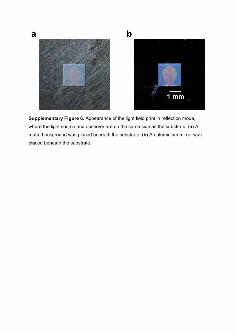
Supplementary Figure 6. Appearance of the light field print in reflection mode,
where the light source and observer are on the same side as the substrate. (a) A
matte background was placed beneath the substrate. (b) An aluminium mirror was
placed beneath the substrate.

Supplementary Note 1 – Geometric equations for raytracing through a lens1 Ignoring higher order terms, the sag z of a rotationally symmetric lens is expressed in
Equation S1:
𝑧𝑧(𝑥𝑥,𝑦𝑦) =𝑥𝑥2 + 𝑦𝑦2
𝑅𝑅 �1 + �1− (1 + 𝐾𝐾) 𝑥𝑥2 + 𝑦𝑦2𝑅𝑅2 �
+ ⋯ (S1)
where (x, y, z) are the cartesian coordinates of the lens surface, R is the radius of
curvature at the lens vertex, and K is the conic constant. We set K = 0 (spherical case)
and R = 22 µm.
Due to the rotational symmetry of the lens, analysis of the lens profile is simplified by
considering only its sagittal cross-section (y = 0). On this plane, the angle σ that the
normal of the lens surface makes with the optical axis is expressed in Equation S2:
𝑡𝑡𝑡𝑡𝑡𝑡 𝜎𝜎 =𝜕𝜕𝜕𝜕𝜕𝜕𝑥𝑥 =
𝑥𝑥𝑅𝑅(1 + 𝜀𝜀)�2 +
(1 + 𝐾𝐾)(𝑥𝑥2 + 𝑦𝑦2)𝜀𝜀(1 + 𝜀𝜀)𝑅𝑅2 �+ ⋯ (S2)
where 𝜀𝜀 = �1− (1 + 𝐾𝐾) 𝑥𝑥2+𝑦𝑦2
𝑅𝑅2.
Once the normal of the lens surface is known, rays are traced through the lens by
applying Snell’s Law, which is expressed in Equation S3.
𝑡𝑡1 sin 𝜃𝜃1 =𝑡𝑡2 sin 𝜃𝜃2 (S3)
where n1 and n2 are the refractive index of the first medium and second medium
respectively, θ1 is the angle of incidence, and θ2 is the angle of refraction.

Supplementary Note 2 – Calculation of CIE XYZ and xy coordinates2 The CIE tristimulus values (X, Y, Z) are expressed in Equations S4 – S7:
𝑋𝑋 = 𝑘𝑘�𝑇𝑇(𝜆𝜆)𝑆𝑆(𝜆𝜆)�̅�𝑥(𝜆𝜆)𝛥𝛥𝜆𝜆780
380
(S4)
𝑌𝑌 = 𝑘𝑘�𝑇𝑇(𝜆𝜆)𝑆𝑆(𝜆𝜆)𝑦𝑦�(𝜆𝜆)𝛥𝛥𝜆𝜆780
380
(S5)
𝑍𝑍 = 𝑘𝑘�𝑇𝑇(𝜆𝜆)𝑆𝑆(𝜆𝜆)𝑧𝑧̅(𝜆𝜆)𝛥𝛥𝜆𝜆780
380
(S6)
where
𝑘𝑘 = 100/�𝑆𝑆(𝜆𝜆)𝑦𝑦�(𝜆𝜆)𝛥𝛥𝜆𝜆780
380
(S7)
𝑘𝑘 is the normalizing factor, 𝑇𝑇(𝜆𝜆) is the transmittance of the pixel, 𝑆𝑆(𝜆𝜆) is the relative
spectral power of a CIE standard illuminant, �̅�𝑥(𝜆𝜆) , 𝑦𝑦�(𝜆𝜆) and 𝑧𝑧̅(𝜆𝜆) are the colour
matching functions of a CIE standard observer, and 𝛥𝛥𝜆𝜆 is the wavelength
measurement interval.
The CIE chromaticity coordinates (x, y) are then calculated from Equations S8 – S9:
𝑥𝑥 =𝑋𝑋
𝑋𝑋 + 𝑌𝑌 + 𝑍𝑍 (S8)
𝑦𝑦 =𝑌𝑌
𝑋𝑋 + 𝑌𝑌 + 𝑍𝑍 (S9)
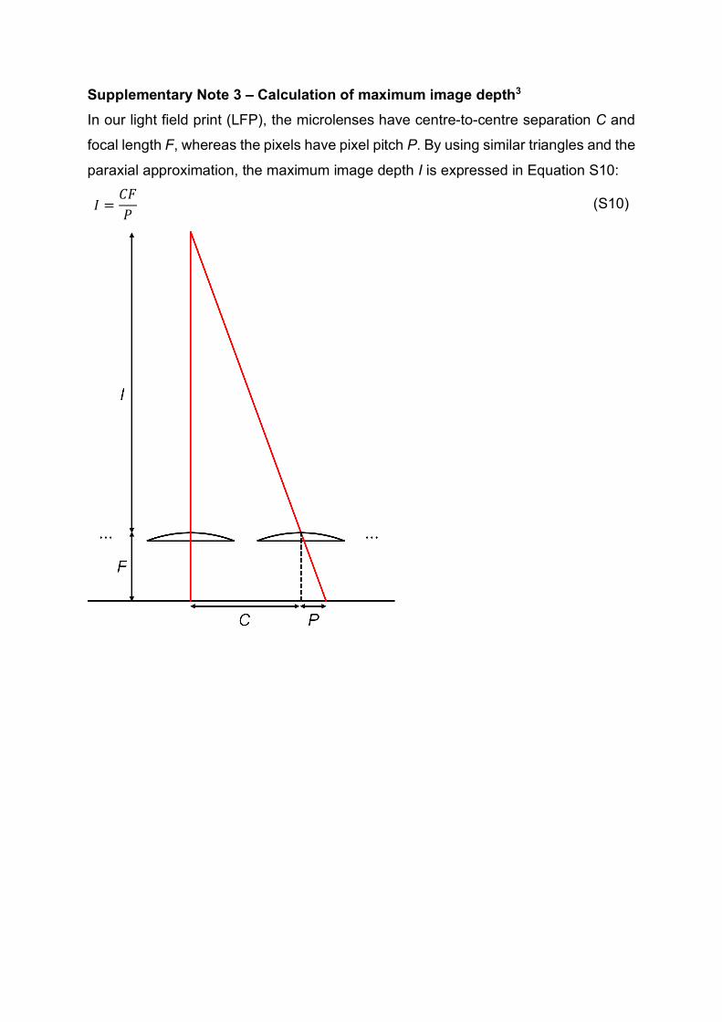
Supplementary Note 3 – Calculation of maximum image depth3 In our light field print (LFP), the microlenses have centre-to-centre separation C and
focal length F, whereas the pixels have pixel pitch P. By using similar triangles and the
paraxial approximation, the maximum image depth I is expressed in Equation S10:
𝐼𝐼 =𝐶𝐶𝐶𝐶𝑃𝑃 (S10)

Supplementary References
1 Mikš, A., Novák, P. & Novák, J. Calculation of aberration and direction of a normal to aspherical surface. Opt. Laser Technol. 45, 708-712 (2013).
2 ASTM International. Standard Practice for Computing the Colors of Objects by Using the CIE System. ASTM E308-01 (2001).
3 Kim, Y. M., Choi, K.-H. & Min, S.-W. Analysis on expressible depth range of integral imaging based on degree of voxel overlap. Appl. Opt. 56, 1052-1061 (2017).