Embed Size (px)
Citation preview

Sensors, Cameras, and Systems for Industrial/Scientific Applications X, Edited by Erik Bodegom, Valerie Nguyen, Proc. of SPIE-IS&T Electronic Imaging, SPIE Vol. 7249, 72490R
Copyright 2009 SPIE-IS&T. One print or electronic copy may be made for personal use only. Systematic reproduction and distribution, duplication of any material in this paper for a fee or for commercial purposes, or modification of the
content of the paper are prohibited. CCC code: 0277-786X/09/$18 http://dx.doi.org/10.1117/12.806272
High quantum efficiency, back-illuminated, crystallographically etched, silicon-on-sapphire avalanche photodiode with very wide
dynamic range, for manufacturable high resolution imaging arrays
A.G. Stern*a, Daniel C. Coleb
aDept. of Electrical Eng., Boston Univ., 8 St. Mary’s St., Boston, MA, USA 02215; bDept. of Manufacturing Eng., Boston Univ., 15 St. Mary’s St., Brookline, MA, USA 02446;
ABSTRACT
There is a growing need in industrial and scientific research applications for very wide dynamic range, high sensitivity imaging methods. To fill this need, an advanced back-illuminated avalanche photodiode (APD) design is presented based on crystallographically etched (100) epitaxial silicon on R-plane sapphire (SOS), enabling large single photon sensitive, solid-state focal plane arrays with very wide dynamic range. The design will enable reliable and low cost fabrication. When (100) silicon is properly etched with KOH:IPA:H2O solution through a thermally grown oxide mask, square based pyramidal frustum or mesa arrays result with the four mesa sidewalls of the APD formed by (111) silicon planes that intersect the (100) planes at a crystallographic angle, φc = 54.7°. The APD is fabricated in the silicon mesa. Very wide dynamic range operation at high quantum efficiencies exceeding 50% for 250 nm< λ<400 nm and exceeding 80% for 400 nm< λ<700 nm, is enabled by a carefully optimized p-type boron spatial impurity profile, fabricated by high temperature diffusion. Monte Carlo modeling confirms the majority of electron-hole pairs are photogenerated outside of the narrow device multiplication region, resulting in a very low APD excess noise factor.
Keywords: silicon APD arrays, back-illuminated, high quantum efficiency, silicon-on-sapphire, crystallographically selective etching, sapphire microlens, sensitive-area-fill-factor, optical cross-talk
1. INTRODUCTION We present in this paper a novel back-illuminated APD device design that enables the fabrication of low cost, high-performance silicon APD arrays. The method enables high quantum efficiency, formed with 27 µm square pixels for high resolution imaging with 100% sensitive-area-fill-factor, on a mechanically rugged and optically transparent sapphire substrate. To the best of our knowledge, a solid-state APD camera has not been designed before that employs APD devices that can be used in both linear and Geiger-mode with high quantum efficiency. This paper describes much about how this wide dynamic range design can be achieved. When (100) silicon is properly etched with KOH:IPA:H2O solution through a thermally grown oxide mask, square based pyramidal frustum or mesa arrays result with the four mesa sidewalls of the APD formed by (111) silicon planes that intersect the (100) planes at a crystallographic angle, φc = 54.7°. [1] The APD is fabricated in the mesa using conventional silicon processing technology and is specially designed to operate over a wide dynamic range in a dual-mode, operating in a linear mode with or without internal gain for passive imaging in daylight conditions and in single-photon sensitive Geiger-mode for active or passive imaging under low-light level conditions. The detector is back-illuminated through a light focusing spherical microlens fabricated in the thinned sapphire substrate that directs light toward the device interior and away from the silicon mesa sidewalls, thereby compensating the optical dead space between pixels resulting from the mesa isolation etch and also from the internal device guard diode geometry. The sapphire microlenses can be coated with an antireflective (λ/4) MgF2 layer, to improve the optical power transmittance from air into the sapphire. In addition, a lattice matched aluminum nitride (AlN) antireflective crystal layer can be grown at the sapphire-silicon interface to further increase the optical power transmittance into the device silicon as shown in Fig. 1. The APDs in the array share a common, front-side anode contact, made locally at the base of each device mesa. A low resistance aluminum (Al) or copper (Cu) metal anode grid fills the space between pixels and also *[email protected]; phone 1 617 669-6029; fax 1 617 353-8381; bu.edu

Sensors, Cameras, and Systems for Industrial/Scientific Applications X, Edited by Erik Bodegom, Valerie Nguyen, Proc. of SPIE-IS&T Electronic Imaging, SPIE Vol. 7249, 72490R
Copyright 2009 SPIE-IS&T. One print or electronic copy may be made for personal use only. Systematic reproduction and distribution, duplication of any material in this paper for a fee or for commercial purposes, or modification of the
content of the paper are prohibited. CCC code: 0277-786X/09/$18 http://dx.doi.org/10.1117/12.806272
functions to inhibit optical cross-talk by shielding adjacent detectors from stray photons generated during the avalanche process. SOS-APD arrays are indium bump-bonded to CMOS readout ICs to produce hybrid focal plane arrays (FPAs) as shown in Fig. 2, which might be 1024x1024 pixels or larger. [2,3] The camera lens focal length and focal ratio maintain 100% sensitive-area-fill-factor over the full FPA active area by limiting the maximum incidence angle of the extreme rays shown in red in Fig. 2, incident at the microlens edges of the pixel, located farthest from the camera optic axis at the corner of the FPA.
Fig. 1: Advanced back-illuminated, crystallographically etched silicon-on-(R-plane) sapphire APD device for arrays, showing a monolithically integrated sapphire microlens and λ/4-MgF2 and AlN antireflective layers.
Fig. 2: Back-illuminated, silicon-on-sapphire APD array chip, bump-bonded to CMOS readout-IC. Extreme rays (shown in red) are incident at the maximum incidence angle θ1-max.
The silicon APD is designed with a carefully optimized high electric field multiplication region, fabricated by high temperature diffusion of boron. The boron impurity profile needs to be optimized for several purposes. This profile essentially determines the spatial electric field in the device as well as the boundary between the low-electric-field absorption-collection region and the high-electric-field multiplication region, plus the APD guard diode geometry. The guard diode boundary function fgd(x,y), shown in Fig. 1 describes the latter geometry. The narrow, high electric field multiplication region and the much wider low electric field collection-absorption region, help to provide stable, uniform gain with minimum variance, for nearly all of the photogenerated electrons in the device. Since most electron-hole pairs (EHPs) are generated through light absorption outside of the multiplication region, this results in a low excess noise factor for the APD. [4]
2. SILICON-ON-SAPPHIRE MATERIAL SYSTEM FOR APD ARRAYS The capability of Czochralski grown R-plane sapphire crystal substrates to support the epitaxial growth of (100) oriented silicon, was discovered in 1963 by researchers at the Boeing corporation. Since the initial discovery, SOS technology has been applied primarily for producing high speed, radiation resistant CMOS circuits for use in space applications. In fact, the microprocessor aboard the Voyager space craft launched in 1977 was fabricated using silicon-on-sapphire and it still continued to function in 2006, three years after the craft had exited the earth’s solar system. In the early years of SOS technology, material challenges provided the main obstacle to its rapid commercialization for VLSI-CMOS transistor fabrication. The relatively large lattice mismatch between atoms in the silicon crystal and atoms of the sapphire R-plane, resulted in high defect concentrations in the thin device silicon near the sapphire interface where FET transistors were fabricated. High defect concentrations in the epitaxial silicon led to low process yields early on, that prevented the technology from becoming cost competitive with bulk silicon CMOS processes. As a result, the technology was only used for special applications that could justify the increased cost.

Sensors, Cameras, and Systems for Industrial/Scientific Applications X, Edited by Erik Bodegom, Valerie Nguyen, Proc. of SPIE-IS&T Electronic Imaging, SPIE Vol. 7249, 72490R
Copyright 2009 SPIE-IS&T. One print or electronic copy may be made for personal use only. Systematic reproduction and distribution, duplication of any material in this paper for a fee or for commercial purposes, or modification of the
content of the paper are prohibited. CCC code: 0277-786X/09/$18 http://dx.doi.org/10.1117/12.806272
A breakthrough occurred in 1979 with the development of a method to improve the silicon crystal quality at the sapphire interface. Silicon ions were implanted using channeling, to amorphise the higher defect density silicon near to the sapphire interface while leaving the higher quality silicon closer to the epitaxial surface undamaged. [5] The substrate was subsequently annealed to recrystallize the silicon near the sapphire interface using the high quality silicon at the top, as a template for crystal growth. By the early 1990s, SOS-CMOS technology had become viable commercially for high speed RF-CMOS circuit applications. Although silicon-on-sapphire was originally developed for integrated circuit applications, it also has many ideal attributes for use as a substrate material, supporting back-illuminated, solid-state, silicon detector arrays. Sapphire is an anisotropic, dielectric crystal of the negative uniaxial type that is weakly birefringent (no-ne= 0.008); it possesses broadband optical transmittance ranging from the deep ultraviolet (λo = 200 nm) to the midwave IR (λo = 5500 nm). Sapphire is extremely resilient, supporting thinning below 100 µm which is an important requirement for high resolution back-illuminated detector arrays. Sapphire can be optically polished to better than an 80-50 surface finish and can be etched optically using 157 nm excimer laser ultraviolet light to fabricate light focusing microlenses for the silicon detectors. Sapphire is chemically resistant to most liquid etchants at room temperature and therefore functions as an ideal etchstop material during liquid crystallographic etching with KOH:IPA:H2O solution to define the silicon pixel mesa arrays. To enable high quantum efficiency, back-illuminated silicon detector arrays, the refractive index mismatch between air, sapphire and silicon has to be corrected however. The wide bandgap semiconductor material AlN, is closely lattice matched and refractive index matched to both sapphire and silicon and offers the prospect of enabling fabrication of high transmittance (100) silicon-on-(AlN)-sapphire substrates for back-illuminated silicon imagers. Aluminum nitride is a birefringent, direct bandgap semiconductor of the positive uniaxial type (no < ne), and possesses a room temperature bandgap Eg-AlN = 6.13 eV, corresponding to a wavelength λEg = (hco)/qEg-AlN = 201.5 nm. High quality crystalline material shows excellent optical transmittance for TE and TM polarized waves and can be considered a lossless dielectric for λo ≥ 250 nm. We have shown in Ref. 6 that the atoms occupying positions in the AlN A-plane match the symmetry of both the sapphire R-plane atoms and the silicon (100) atoms. The lattice mismatch between AlN atoms and R-plane sapphire atoms is 4.8% in the direction parallel to the AlN A-plane and normal to the [100] direction while the mismatch is 4.5% in the [001] c-axis direction of AlN. The lattice mismatch between AlN atoms and (100) silicon atoms is 0.8% and 8.3% respectively. A review of the literature shows that A-plane AlN can in fact be grown on R-plane sapphire; this fact strengthens the possibility of also being able to grow (100) epitaxial silicon on R-plane sapphire having a thin (< 100 nm thick) lattice matched AlN single crystal antireflective layer. [7,8,9] Such epitaxial growth would produce novel silicon-on-(AlN)-sapphire substrates for low-cost, high quantum efficiency, back-illuminated silicon optoelectronics. At the air-sapphire interface, a single (λ/4) MgF2 antireflective layer provides almost unity optical power transmittance from air into sapphire at the design wavelength. MgF2 has a low refractive index and is used commonly as an antireflective coating for sapphire and conventional glass optics. At the sapphire silicon interface, AlN provides the required lattice matching between R-plane sapphire and (100) silicon and in addition, can provide refractive index matching to enhance the optical power transmitted into the device silicon from sapphire over a broad wavelength range [10,11]. In Ref. 6 we calculated the back-illuminated optical power transmittance into silicon through the MgF2(82 nm)-sapphire-AlN(82 nm) dielectric stack to be greater than 50% for wavelengths between 250 nm and 400 nm and greater than 80% for wavelengths between 400 nm and 700 nm. 2.1 High quantum efficiency crystallographically etched silicon pixel design Silicon on R-plane sapphire substrates support a reliable and low cost method for fabricating large area, high resolution silicon APD arrays with 27 µm pixels or smaller by using the anisotropic, crystallographically selective liquid etchant KOH:IPA:H2O or TMAH (trimethyl ammonium hydroxide), to define an array of square based silicon pixels or device mesas that are electrically isolated from each other. [12] The dielectric sapphire substrate acts as a natural etchstop barrier, ensuring that all mesas are uniformly etched to the same height and are fully isolated electrically from each other. Anisotropic, crystallographically selective liquid etching is performed through a hard silicon dioxide mask which is deposited or thermally grown on the epitaxial silicon prior to the crystallographic etching step. Openings are patterned and etched in the hard SiO2 mask using photolithography and isotropic etching of the SiO2 with aqueous HF or a buffered oxide etching solution. Figure 3 shows a hard oxide mask with aperture that could be used to

Sensors, Cameras, and Systems for Industrial/Scientific Applications X, Edited by Erik Bodegom, Valerie Nguyen, Proc. of SPIE-IS&T Electronic Imaging, SPIE Vol. 7249, 72490R
Copyright 2009 SPIE-IS&T. One print or electronic copy may be made for personal use only. Systematic reproduction and distribution, duplication of any material in this paper for a fee or for commercial purposes, or modification of the
content of the paper are prohibited. CCC code: 0277-786X/09/$18 http://dx.doi.org/10.1117/12.806272
crystallographically etch a 3x3 pixel array of APD device mesas. Crystallographic directions for the underlying silicon are also indicated.
Fig 3: SiO2 hard mask design showing the aperture for crystallographically etching a square based silicon mesa frustum array. Anisotropic liquid etching with KOH:IPA:H2O or TMAH solution allows the precise and rapid fabrication of large area APD arrays with small pixel sizes for high spatial resolution imaging FPAs. The APD array design presented here has square pixels as shown in Fig. 3 with a side length of 27 µm and a mesa height of 10 µm. Although, smaller pixel sizes can be fabricated by anisotropic liquid etching, the fixed angle φc = 54.7° between the (100) and (111) planes in silicon constrains the mesa top area and the height of the mesa. Increasing the mesa height to improve the absorption efficiency of light in silicon reduces the mesa top area which needs to remain large enough to accommodate an indium metal solder bump of at least 15 µm in diameter in order not to sacrifice bump fabrication yields. A pixel size of 27 µm with mesa height h = 10 µm therefore represents a good compromise between the need for high resolution and light absorption efficiency while supporting a square mesa pixel top area with a side length of nearly 13 µm for reliable indium bump fabrication. [3] High photodetector quantum efficiency is critical for APD device performance and is described by Eq. (1).
( ) ( )( )[ ]ζη λα heff eR −−−= 11 (1)
Three terms in Eq. (1) contribute to the overall APD photodetector quantum efficiency including the optical power transmittance into silicon given by the first term, light absorption efficiency in silicon given by the second term and the collection efficiency ζ, of photogenerated electron-hole pairs (EHPs) that contribute to the photocurrent in the device. The optical power transmittance term T(λ) = (1-R(λ)) was calculated in Ref. 6 as a function of wavelength for TE polarized waves normally incident on the back-illuminated APD substrate. The absorption efficiency term (1-e-α(λ)h) in Eq. (1), describes the efficiency of light absorption in the device silicon and depends on the silicon mesa height h, and the silicon absorption efficiency α(λ). Electrical isolation of APD pixels by crystallographic etching results in a mesa geometry with non-uniform height that depends on position as h(x,y) where x and y are coordinates located in the square base plane area of the pixel. The effective absorption efficiency was calculated in Ref. 6 for the APD pixel with non-uniform height for back-illuminated normally incident light, by integrating the absorption efficiency term from Eq. (1) over the pixel base area followed by a normalization of the result by the base area of the pixel. The maximum attainable quantum efficiency of the APD pixel with and without a microlens was calculated in Ref. 6 assuming uniform TE-wave back-illumination at normal incidence on the pixel base area through the substrate and assuming ideal collection

Sensors, Cameras, and Systems for Industrial/Scientific Applications X, Edited by Erik Bodegom, Valerie Nguyen, Proc. of SPIE-IS&T Electronic Imaging, SPIE Vol. 7249, 72490R
Copyright 2009 SPIE-IS&T. One print or electronic copy may be made for personal use only. Systematic reproduction and distribution, duplication of any material in this paper for a fee or for commercial purposes, or modification of the
content of the paper are prohibited. CCC code: 0277-786X/09/$18 http://dx.doi.org/10.1117/12.806272
efficiency of photogenerated carriers in the device with ζ = 1. With a microlens the quantum efficiency was shown to be greater than 50% for wavelengths between 250 nm and 400 nm and 80% for wavelengths between 400 nm and 700 nm. The collection efficiency term zeta ζ in Eq. (1), represents the fraction of photogenerated EHPs contributing to photocurrent in the device, that are not lost to recombination at defect/trap sites or at the internal APD guard diode structure. A guard diode structure shown in Fig. 1 is necessary in a mesa isolated APD device to collect the surface generated electrons at the passivated (111) sidewalls, thereby preventing them from being transported to the device interior where they can be multiplied to increase device noise. The ζ term is certainly nontrivial to deduce because information is needed about the trap species and their spatial concentrations in the device. Moreover, information about the spatial electric field in the device under bias conditions is also needed to describe photogenerated carrier drift either toward the high electric field multiplication region in the device or toward the guard diode at the periphery of the mesa that is intended ideally to collect only the surface generated noise electrons. For a two terminal APD with a guard diode, an expression for ζ is given by Eq. (2), where β represents the fraction of multiplied photoelectrons and γ represents the fraction of unmultiplied photoelectrons collected by the guard diode. The quantities β and γ sum to unity in the absence of recombination or other carrier loss mechanisms in the device.
Gγβζ += (2)
The multiplication gain value G, appears in the denominator of Eq. (2) because photoelectrons collected by the guard diode are not multiplied by the avalanche gain of the APD and therefore the gain term in the denominator of Eq. (2) cancels the gain term that multiplies the overall APD quantum efficiency ηeff used in calculating the device photocurrent ip. The photocurrent ip includes a contribution from the multiplied and unmultiplied photoelectrons. [11] The quantum efficiency of the APD should always be calculated with G set to unity in Eq. (2). A function fgd(x,y) shown in Fig. 1 that deterministically separates the internal regions of the APD where photogenerated electrons will be collected by the multiplication region or the guard diode is an idealization and does not exist in practice due to the probabilistic nature of charge carrier motion. In Sec. 4 of this paper however, the spatial electric field inside the APD at a fixed reverse bias voltage, is used to evaluate the ζ term in Eq. (1) by the Monte Carlo computational statistical method to obtain precise average values for β and γ for the APD, and to allow the excess noise factor of the internal APD gain G, to be evaluated.
3. WIDE DYNAMIC RANGE SILICON MESA APD DESIGN
To image effectively under all ambient illumination ranging from (1) the extreme AM0 condition in outer space when the APD-FPA imager is staring directly into the sun and the illuminance at the camera lens is approximately 130,000 Lux, to (2) the photon starved case when imaging a scene on a cloudy night with no moon and far away from city lights when the illuminance at the camera lens might be 0.0001 Lux, the APD should be capable of operating in a dual mode. The two modes are a linear mode, with or without internal gain biased below the reverse breakdown voltage, or the single photon sensitive Geiger-mode biased above the reverse breakdown voltage. The APD mode of operation (analog linear or digital Geiger-mode) is selected by the requirement of maximizing the signal to noise ratio (SNR) of the APD-FPA optical receiver. [11,16] The linear mode of operation is appropriate when detected signals are large compared to the noise of the APD optical receiver and would cause the Geiger-mode APD to saturate, such as in daylight imaging applications. In contrast, the Geiger-mode of operation provides large internal APD gain for single photon sensitivity and zero electronic readout noise which is needed for very low light level passive or active imaging. Geiger-mode operation is especially useful for active imaging when the photon returns from an object are well localized temporally as with a pulsed laser, and must be discriminated from background noise uniformly spread out in time. The maximum single photon counting rate for a two terminal silicon APD operating in the Geiger-mode is approximately 1E7 photons per second or about 10 MHz. This detection rate is limited by the minimum dead time of 50 nsec following each avalanche event that is needed to allow charge carriers in the pn-junction to recombine before rearming the APD. [3] Reducing the deadtime below 50 nsec, increases the APD afterpulsing probability and the dark count rate as the unrecombined carriers generated during the previous avalanche event may erroneously retrigger the

Sensors, Cameras, and Systems for Industrial/Scientific Applications X, Edited by Erik Bodegom, Valerie Nguyen, Proc. of SPIE-IS&T Electronic Imaging, SPIE Vol. 7249, 72490R
Copyright 2009 SPIE-IS&T. One print or electronic copy may be made for personal use only. Systematic reproduction and distribution, duplication of any material in this paper for a fee or for commercial purposes, or modification of the
content of the paper are prohibited. CCC code: 0277-786X/09/$18 http://dx.doi.org/10.1117/12.806272
APD. Hence, afterpulsing limits the maximum Geiger-mode count rate of the silicon APD. This criteria enables one to calculate the maximum illuminance at the camera lens below which Geiger-mode operation of the detector is possible. Figure 4 shows the calculated unmultiplied photocurrent of the back-illuminated, crystallographically etched, silicon-on-sapphire APD detector pixel of 27 µm size described in Sec. 2 with quantum efficiency calculated in Ref. 6, for different illuminance (in Lux) at the camera lens having a focal length F = 21 cm and focal ratio setting of f/# = 5.6. In determining the threshold current below which Geiger-mode operation of the APD is possible, it is assumed that all photogenerated electrons comprising the photocurrent, produce a detection event and that the dark current and associated dark count rate is negligible compared to the photogenerated signal current.
Fig. 4: Average unmultiplied photocurrent of a 27 µm APD pixel in a 1024x1024 array with a camera lens having FL = 21 cm and f/# = 5.6. Geiger-mode operation is only possible after late dusk. According to Fig. 4, Geiger-mode operation of the detector without saturation of the count rate is only possible below a photocurrent of ip = 1.6 pA corresponding to an illuminance of less than 1 Lux at the camera lens. Single photon sensitive Geiger-mode imaging therefore only becomes possible after late dusk. The calculation in Fig. 4 confirms the need for wide dynamic range operating capability for the APD detector. Designing an APD that can operate with high quantum efficiency in both the analog linear mode, with or without internal gain and in the digital Geiger-mode when biased above the reverse breakdown voltage, is difficult and has not been successfully implemented yet in a solid-state APD-FPA camera. To operate efficiently, such a device must deplete the p-type silicon fully to the sapphire interface at relatively low reverse bias in the linear mode without gain, to efficiently collect photogenerated electrons near the silicon back surface. Figures 5 and 6 show the crystallographically etched APD mesa pixel in cross-section. Two dimensional ray tracing was performed to illustrate probabilistic photon absorption for 530 nm (Fig. 5) and 800 nm (Fig. 6) TE polarized light which is normally incident to the pixel back surface through a focusing spherical sapphire microlens and 50 µm thick sapphire substrate, as shown in Fig. 1.
Fig. 5: Two dimensional cross-section of Si mesa APD with 50 µm thick sapphire substrate and spherical microlens (not shown). Ray tracing of normally incident TE-waves shows the probabilistic absorption of 530 nm photons.
Fig. 6: Two dimensional cross-section of Si mesa APD with 50 µm thick sapphire substrate and spherical microlens (not shown). Ray tracing of normally incident TE-waves shows the probabilistic absorption of 800 nm photons.

Sensors, Cameras, and Systems for Industrial/Scientific Applications X, Edited by Erik Bodegom, Valerie Nguyen, Proc. of SPIE-IS&T Electronic Imaging, SPIE Vol. 7249, 72490R
Copyright 2009 SPIE-IS&T. One print or electronic copy may be made for personal use only. Systematic reproduction and distribution, duplication of any material in this paper for a fee or for commercial purposes, or modification of the
content of the paper are prohibited. CCC code: 0277-786X/09/$18 http://dx.doi.org/10.1117/12.806272
The simulated, probabilistic nature of photon absorption at 530 nm in Fig. 5 and especially at shorter wavelengths, confirms the need for full depletion of the p-type device silicon to the sapphire interface in order to collect short wavelength photons efficiently. As the reverse bias voltage is increased, the critical electric field (Ec = 3E5 V/cm) in silicon is reached in the more heavily doped multiplication region of the device. Impact ionization occurs above the critical electric field and produces avalanche gain which is useful for linear mode device operation with gain. As the reverse bias voltage is increased to the reverse breakdown voltage, the electric fields become sufficiently large to produce nearly infinite gain in the APD causing a large current to flow that can damage the pn-junction. Biasing the APD above the reverse breakdown voltage is possible however, using digital pixel control circuitry with active quenching that supports operation in the Geiger-mode with zero electronic readout noise. [2,3] The mesa etched silicon APD design we developed is manufacturable and supports high quantum efficiency operation with wide dynamic range in the ultraviolet and visible wavelengths. Figure 7 shows the simulated APD device structure.
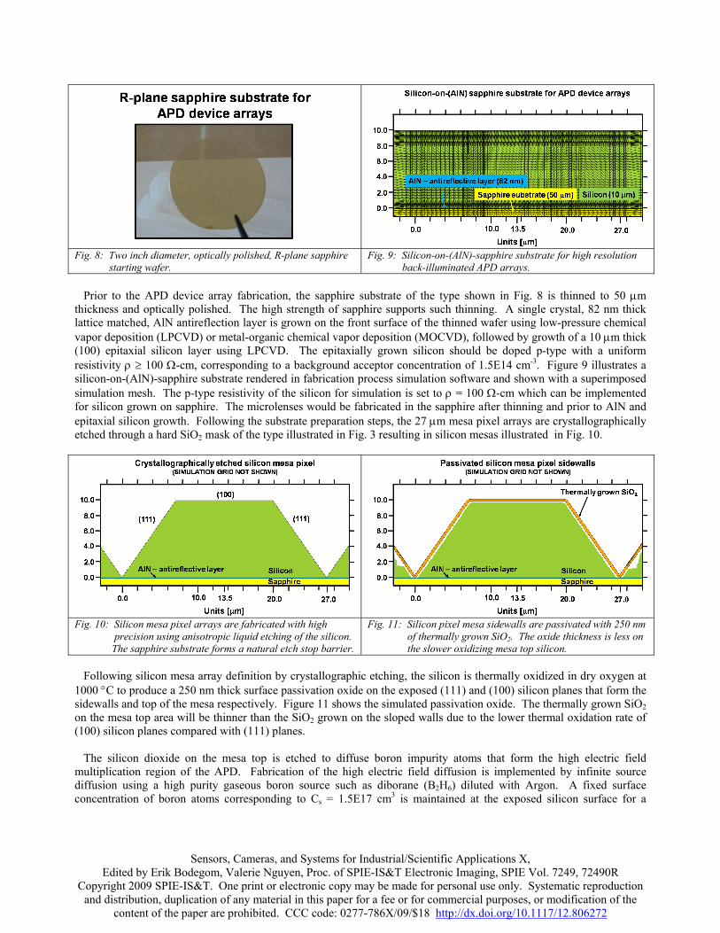
Fig. 7: Simulated silicon APD mesa device structure for arrays. Wide dynamic range APD device operation is achieved by allowing the polysilicon cathode to extend beyond the edges of the mesa top over the thermally grown passivation oxide to form a MOS capacitor which acts as a CCD gate. When the APD is reverse biased, the combination of the APD pn-junction and the MOS capacitor formed by the overhanging polysilicon operate similarly to the input diode and input gate of a CCD. [1] At reverse bias voltages well below the reverse breakdown voltage of the APD, the APD pn-junction cannot deplete fully to the silicon-sapphire interface due to blocking by the high electric field boron impurity diffusion. However, the polysilicon MOS capacitor can deplete into the p-type silicon fully to collect any photogenerated electrons in the device. The APD pn-junction prevents an inversion layer from forming under the polysilicon CCD gate by collecting the photoelectrons under the gate, producing an unmultiplied photocurrent. Therefore, at low reverse bias voltages the polysilicon MOS capacitor depletes deep into the silicon to collect photogenerated electrons that are in turn collected by the cathode of the APD pn-junction, bypassing the high electric field region of the APD without being multiplied. 3.1 Reliable fabrication process for wide dynamic range, silicon mesa APD devices and arrays Fabrication of the crystallographically etched, wide dynamic range silicon APD shown in Fig. 7, can be implemented reliably using well developed silicon processing methods such as thermal oxidation, diffusion, deposition, isotropic liquid etching and photolithography. The starting substrate consists of a sapphire wafer, cut in an off axis direction to expose the R-crystallographic plane at the surface. Figure 8 shows such a substrate which is available commercially.
Sensors, Cameras, and Systems for Industrial/Scientific Applications X, Edited by Erik Bodegom, Valerie Nguyen, Proc. of SPIE-IS&T Electronic Imaging, SPIE Vol. 7249, 72490R
Copyright 2009 SPIE-IS&T. One print or electronic copy may be made for personal use only. Systematic reproduction and distribution, duplication of any material in this paper for a fee or for commercial purposes, or modification of the
content of the paper are prohibited. CCC code: 0277-786X/09/$18 http://dx.doi.org/10.1117/12.806272
Fig. 8: Two inch diameter, optically polished, R-plane sapphire starting wafer.
Fig. 9: Silicon-on-(AlN)-sapphire substrate for high resolution back-illuminated APD arrays.
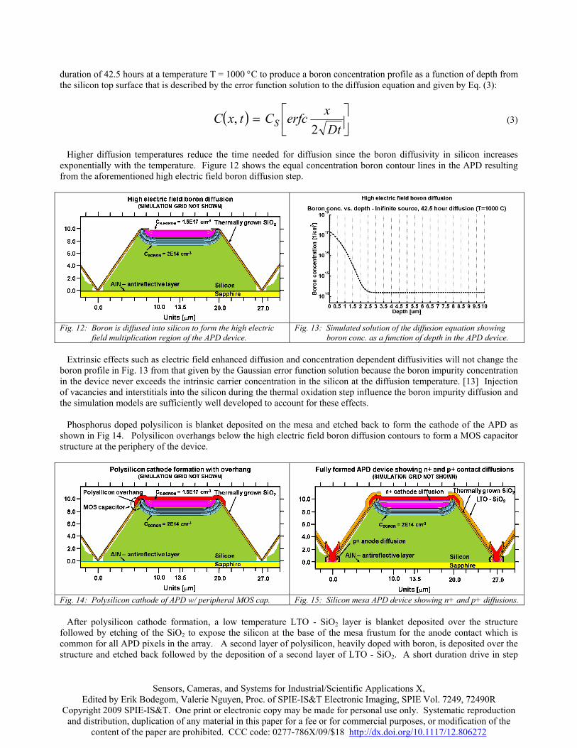
Prior to the APD device array fabrication, the sapphire substrate of the type shown in Fig. 8 is thinned to 50 µm thickness and optically polished. The high strength of sapphire supports such thinning. A single crystal, 82 nm thick lattice matched, AlN antireflection layer is grown on the front surface of the thinned wafer using low-pressure chemical vapor deposition (LPCVD) or metal-organic chemical vapor deposition (MOCVD), followed by growth of a 10 µm thick (100) epitaxial silicon layer using LPCVD. The epitaxially grown silicon should be doped p-type with a uniform resistivity ρ ≥ 100 Ω-cm, corresponding to a background acceptor concentration of 1.5E14 cm-3. Figure 9 illustrates a silicon-on-(AlN)-sapphire substrate rendered in fabrication process simulation software and shown with a superimposed simulation mesh. The p-type resistivity of the silicon for simulation is set to ρ = 100 Ω-cm which can be implemented for silicon grown on sapphire. The microlenses would be fabricated in the sapphire after thinning and prior to AlN and epitaxial silicon growth. Following the substrate preparation steps, the 27 µm mesa pixel arrays are crystallographically etched through a hard SiO2 mask of the type illustrated in Fig. 3 resulting in silicon mesas illustrated in Fig. 10.
Fig. 10: Silicon mesa pixel arrays are fabricated with high precision using anisotropic liquid etching of the silicon. The sapphire substrate forms a natural etch stop barrier.
Fig. 11: Silicon pixel mesa sidewalls are passivated with 250 nm of thermally grown SiO2. The oxide thickness is less on the slower oxidizing mesa top silicon.
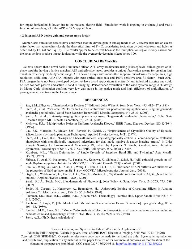
Following silicon mesa array definition by crystallographic etching, the silicon is thermally oxidized in dry oxygen at 1000 °C to produce a 250 nm thick surface passivation oxide on the exposed (111) and (100) silicon planes that form the sidewalls and top of the mesa respectively. Figure 11 shows the simulated passivation oxide. The thermally grown SiO2 on the mesa top area will be thinner than the SiO2 grown on the sloped walls due to the lower thermal oxidation rate of (100) silicon planes compared with (111) planes. The silicon dioxide on the mesa top is etched to diffuse boron impurity atoms that form the high electric field multiplication region of the APD. Fabrication of the high electric field diffusion is implemented by infinite source diffusion using a high purity gaseous boron source such as diborane (B2H6) diluted with Argon. A fixed surface concentration of boron atoms corresponding to Cs = 1.5E17 cm3 is maintained at the exposed silicon surface for a
Sensors, Cameras, and Systems for Industrial/Scientific Applications X, Edited by Erik Bodegom, Valerie Nguyen, Proc. of SPIE-IS&T Electronic Imaging, SPIE Vol. 7249, 72490R
Copyright 2009 SPIE-IS&T. One print or electronic copy may be made for personal use only. Systematic reproduction and distribution, duplication of any material in this paper for a fee or for commercial purposes, or modification of the
content of the paper are prohibited. CCC code: 0277-786X/09/$18 http://dx.doi.org/10.1117/12.806272
duration of 42.5 hours at a temperature T = 1000 °C to produce a boron concentration profile as a function of depth from the silicon top surface that is described by the error function solution to the diffusion equation and given by Eq. (3):
( ) ⎥⎦⎤
⎢⎣⎡=
DtxerfcCtxC S 2
, (3)
Higher diffusion temperatures reduce the time needed for diffusion since the boron diffusivity in silicon increases exponentially with the temperature. Figure 12 shows the equal concentration boron contour lines in the APD resulting from the aforementioned high electric field boron diffusion step.
Fig. 12: Boron is diffused into silicon to form the high electric field multiplication region of the APD device.
Fig. 13: Simulated solution of the diffusion equation showing boron conc. as a function of depth in the APD device.
Extrinsic effects such as electric field enhanced diffusion and concentration dependent diffusivities will not change the boron profile in Fig. 13 from that given by the Gaussian error function solution because the boron impurity concentration in the device never exceeds the intrinsic carrier concentration in the silicon at the diffusion temperature. [13] Injection of vacancies and interstitials into the silicon during the thermal oxidation step influence the boron impurity diffusion and the simulation models are sufficiently well developed to account for these effects. Phosphorus doped polysilicon is blanket deposited on the mesa and etched back to form the cathode of the APD as shown in Fig 14. Polysilicon overhangs below the high electric field boron diffusion contours to form a MOS capacitor structure at the periphery of the device.
Fig. 14: Polysilicon cathode of APD w/ peripheral MOS cap. Fig. 15: Silicon mesa APD device showing n+ and p+ diffusions. After polysilicon cathode formation, a low temperature LTO - SiO2 layer is blanket deposited over the structure followed by etching of the SiO2 to expose the silicon at the base of the mesa frustum for the anode contact which is common for all APD pixels in the array. A second layer of polysilicon, heavily doped with boron, is deposited over the structure and etched back followed by the deposition of a second layer of LTO - SiO2. A short duration drive in step

Sensors, Cameras, and Systems for Industrial/Scientific Applications X, Edited by Erik Bodegom, Valerie Nguyen, Proc. of SPIE-IS&T Electronic Imaging, SPIE Vol. 7249, 72490R
Copyright 2009 SPIE-IS&T. One print or electronic copy may be made for personal use only. Systematic reproduction and distribution, duplication of any material in this paper for a fee or for commercial purposes, or modification of the
content of the paper are prohibited. CCC code: 0277-786X/09/$18 http://dx.doi.org/10.1117/12.806272
diffuses phosphorus from the cathode polysilicon and boron from the anode polysilicon into the device to form the n+ and p+ regions of the APD pn-junction. The APD device thus formed in Fig. 15 is ready for back end processing which includes silicidation of the polysilicon with TiSi2 to form the adhesion/contact layer. A 1 µm thick LTO-SiO2 layer is then deposited over the mesa APDs to provide robust encapsulation of the mesas to help withstand the mechanical stresses of bump bonding. Via holes are etched in the thick LTO-SiO2 and TiN is deposited as a barrier/adhesion layer before and after tungsten via formation. Aluminum metal is deposited and reflowed to form the anode and cathode contact terminals of the APD. The aluminum at the anode also functions to inhibit optical cross-talk between neighboring pixels in the array. The fabrication process described is both reliable and cost effective to implement in existing silicon foundries to produce the final APD device and array structure shown in Fig. 7. During operation, the APD is reverse biased and the polysilicon at the peripheral MOS structure acts as a CCD gate to deplete the silicon bulk fully at reverse bias voltages below the avalanche breakdown voltage of the APD. This unique design feature enables the APD to operate with high quantum efficiency over a wide dynamic range in either the linear mode with gain or in the Geiger-mode. Many variations are possible on the basic design of the wide dynamic range crystallographically etched mesa pixel described above, including double crystallographic etching of the mesa to fabricate a step pyramid with the step near the top of the main mesa frustum. Such a design would allow the high electric field boron diffusion to be prepared epitaxially rather than by thermal diffusion, resulting in a more spatially uniform doping profile in the lateral and depth dimensions, and also a more abrupt transition in boron concentration between the background and high electric field doping regions. The advantage would be an APD with even greater gain uniformity and reduced gain excess noise factor. It is shown in Sec. 4, however, that the present wide dynamic range APD structure of Fig. 7 with carefully optimized high electric field boron diffusion and MOS capacitor is capable of providing stable operation with very low gain noise, obviating the need for more elaborate designs that increase the device complexity and cost of fabrication. 4. PERFORMANCE EVALUATION OF THE APD DESIGN BY MONTE CARLO SIMULATION To evaluate the performance of the silicon mesa APD device structure shown in Fig. 7, a semiconductor equation solver tool (Medici) was used to solve Poisson’s equation in two spatial dimensions. Boundary conditions were applied to the structure in Fig. 16 and the resulting spatial electric field was calculated. Figure 16 on the left shows the equipotential contours and electric field lines from device simulation at the low reverse bias voltage of 28 V, which is 8 V below the 36 V breakdown voltage of the APD. At low reverse bias, the photogenerated electrons are mainly directed toward the MOS capacitor at the periphery of the device and relatively few photogenerated electrons in the APD reach the high electric field multiplication region. Therefore, the internal gain of the device is low even though the electric field in the multiplication region does reach the critical value of 3E5 V/cm in silicon required for impact ionization.
Fig. 16: APD device simulation showing equipotential contours and electric field lines for reverse bias voltages of 28 V (left) and 44 V (right). The reverse breakdown voltage of the APD is 36 V and the p-type silicon background resistivity is 100 Ω-cm.

Sensors, Cameras, and Systems for Industrial/Scientific Applications X, Edited by Erik Bodegom, Valerie Nguyen, Proc. of SPIE-IS&T Electronic Imaging, SPIE Vol. 7249, 72490R
Copyright 2009 SPIE-IS&T. One print or electronic copy may be made for personal use only. Systematic reproduction and distribution, duplication of any material in this paper for a fee or for commercial purposes, or modification of the
content of the paper are prohibited. CCC code: 0277-786X/09/$18 http://dx.doi.org/10.1117/12.806272
Figure 16 on the right shows the equipotential contour change when the APD is reverse biased at 44 V, corresponding to an 8 V bias value above the reverse breakdown voltage of the APD. The result is a much larger fraction of photogenerated electrons directed toward the high electric field multiplication region of the APD than for the lower bias voltage on the left resulting in more internal gain. In both examples, the silicon is fully depleted to enable efficient collection of photogenerated electrons from the entire device volume. 4.1 Evaluation of the fractions of multiplied and unmultiplied photogenerated electrons Monte Carlo simulation is effective for estimating the fractions of the multiplied and unmultiplied photogenerated electrons in the APD. The spatial electric field calculated by device simulation at 44 V reverse bias and shown on the right in Fig. 16, can be imported into Matlab software and Newton’s classical equation of motion is solved for photogenerated electrons and holes to trace their trajectory in the device under influence of the electric field for different optical wavelengths used to generate the electron hole pairs as shown in Figs. 5 and 6. The probability for electrons and holes in the device to generate additional electron hole pairs through impact ionization is calculated using the ionization rates for electrons and holes in silicon that depend on the energy of the carriers according to Eq. (4) and Eq. (5) respectively [14,15].
( ) ( )[ ] 6.411 1.1102 eVe −×=Γ εε (4)
( ) ( )[ ] ( )( ) 0.4120.69 45.11011.1102 eVeVh −×+−×=Γ εεε (5) Figure 17 shows the calculated spatial electric field in the APD device mapped into Matlab software at 44 V reverse bias. Figure 18 shows the average values of β and γ calculated by Monte Carlo simulation as a function of the wavelength for electrons in the APD. These quantities were introduced in Eq. (2) and represent the fractions of multiplied and unmultiplied photogenerated electrons in the APD. It is assumed that no loss mechanisms exist for photogenerated electrons in the APD and all are either multiplied in the high field region or are not multiplied but still collected to contribute to the APD photocurrent with β + γ = 1.
Fig. 17: Mesa APD biased at 44 V for Geiger-mode operation showing the electric field for Monte Carlo simulation.
Fig. 18: Efficiency of collection and multiplication of photogenerated electronsin the APD at 44 V bias.
In Fig. 18 it is apparent that at longer wavelengths the efficiency of collection of photogenerated electrons into the multiplication region of the APD given by β, is lower than for visible wavelengths. The result is expected because longer wavelength light is absorbed more uniformly throughout the 10 µm thickness of the device as seen in Fig. 6, and therefore some electrons are created above the high field multiplication region where they will not be multiplied. In addition, the spatial electric field in Fig. 16 on the right also indicates that some of the electrons created near the left and right central regions of the device will be transported to the periphery of the multiplication region where the probability
Sensors, Cameras, and Systems for Industrial/Scientific Applications X, Edited by Erik Bodegom, Valerie Nguyen, Proc. of SPIE-IS&T Electronic Imaging, SPIE Vol. 7249, 72490R
Copyright 2009 SPIE-IS&T. One print or electronic copy may be made for personal use only. Systematic reproduction and distribution, duplication of any material in this paper for a fee or for commercial purposes, or modification of the
content of the paper are prohibited. CCC code: 0277-786X/09/$18 http://dx.doi.org/10.1117/12.806272
for impact ionizations is lower due to the reduced electric field. Simulation work is ongoing to evaluate β and γ as a function of wavelength for the APD at 28 V applied bias. 4.2 Internal APD device gain and excess noise factor Monte Carlo simulation results have confirmed that the device gain in analog mode at 28 V reverse bias has an excess noise factor that approaches closely the theoretical limit of F = 2, considering ionization by both electrons and holes as described by Eq. (4) and Eq. (5). The results appear to be correct because the multiplication region is very narrow and the holes seldom produce impact ionization while the average device gain is kept below 100.
CONCLUDING REMARKS We have shown that a novel back-illuminated silicon APD array architecture using (100) epitaxial silicon grown on R-plane sapphire having a lattice matched AlN antireflective layer, provides a unique fabrication means for creating high quantum efficiency, wide dynamic range APD device arrays with monolithic sapphire microlenses for large area, high resolution, solid-state APD-FPA imagers with zero optical cross talk and 100% sensitive-area-fill-factor. Such APD-FPA imagers have not been developed before, yet have broad applications in scientific and industrial imaging and could be used for both passive and active 2D and 3D imaging. Performance evaluation of the wide dynamic range APD design by Monte Carlo simulation confirms very low gain noise in the analog mode and high efficiency of multiplication of photogenerated electrons in the Geiger-mode.
REFERENCES [1] Sze, S.M., [Physics of Semiconductor Devices 2nd Edition], John Wiley & Sons, New York, 495, 412-427, (1981). [2] Stern, A., et al., “Scalable CMOS readout circuit architecture for photo-counting applications using Geiger-mode
avalanche photodiodes,” Solid State Research Report MIT Lincoln Laboratory, (4), 25-30, (2001). [3] Stern, A., et al., “Intensity-imaging focal plane array using Geiger-mode avalanche photodiodes,” Solid State
Research Report MIT Lincoln Laboratory, (4), 23-31, (2003). [4] McIntyre, R.J., “Multiplication Noise in Uniform Avalanche Diodes,” IEEE Trans. Electron Devices, ED-13(164),
(1966). [5] Lau, S.S., Matteson, S., Mayer, J.W., Revesz, P., Gyulai, J., “Improvement of Crystalline Quality of Epitaxial
Silicon Layers by Ion-Implantation Techniques,” Applied Physics Letters, 34(1), (1979). [6] Stern, A.G., Cole, D.C., “Design of a back-illuminated, crystallographically etched, silicon-on-sapphire avalanche
photodiode with monolithically integrated microlens, for dual-mode passive & active imaging arrays,” in Lidar Remote Sensing for Environmental Monitoring IX, edited by Upendra N. Singh, Kazuhiro Asai, Achuthan Jayaraman, Proceedings of SPIE Vol. 7153, (SPIE, Bellingham, WA, 2008) 71530Z.
[7] Kronberg, M.L., “Plastic Deformation of Single Crystals of Sapphire: Basal Slip and Twinning,” Acta Metall., 5(507), (1957).
[8] Shibata, T., Asai, K., Nakamura, Y., Tanaka, M., Kaigawa, K., Shibata, J., Sakai, H., “AlN epitaxial growth on off-angle R-plane sapphire substrates by MOCVD,” J. of Crystal Growth, 229(1), 63-68, (2001).
[9] Luo, W., Wang, X., Guo, L., Xiao, H., Wang, C., Ran, J., Li, J., Li, J., “Influence of AlN buffer layer thickness on the properties of GaN epilayer on Si(111) by MOCVD,” Microelectronics Journal, Jan., (2008).
[10] Ozgür, Ü., Webb-Wood, G., Everitt, H.O., Yun, F., Morkoc, H., “Systematic measurement of AlxGa1-xN refractive indices,” Applied Physics Letters, 79(25), (2001).
[11] Saleh, B.E.A., Teich, M.C., [Fundamentals of Photonics], John Wiley & Sons, New York, 246-253, 755, 789, (2007).
[12] Seidel, H., Cspergi, L., Heuberger, A., Baumgärtel, H., “Anisotropic Etching of Crystalline Silicon in Alkaline Solutions,” J. Electrochem. Soc., 137(11), 3612-3625 (1990).
[13] Plummer, J.D., Deal, M.D., Griffin, P.D., [Silicon VLSI Technology], Prentice Hall, Upper Saddle River NJ, 618-619, (2000).
[14] Jacoboni, C., Lugli, P., [The Monte Carlo Method for Semiconductor Device Simulation], Springer-Verlag, Wien, 104-113, (1989).
[15] Fischetti, M.V., Laux, S.E., “Monte Carlo analysis of electron transport in small semiconductor devices including band-structure and space-charge effects,” Phys. Rev. B, 38(14), 9721-9745, (1988).
[16] Stern, A.G., (Ph.D. thesis calculations)