Embed Size (px)
Citation preview

University of Pennsylvania University of Pennsylvania
ScholarlyCommons ScholarlyCommons
Publicly Accessible Penn Dissertations
2013
High Performance Optical Transmitter Ffr Next Generation High Performance Optical Transmitter Ffr Next Generation
Supercomputing and Data Communication Supercomputing and Data Communication
Xiaotie Wu University of Pennsylvania, [email protected]
Follow this and additional works at: https://repository.upenn.edu/edissertations
Part of the Communication Commons, and the Electrical and Electronics Commons
Recommended Citation Recommended Citation Wu, Xiaotie, "High Performance Optical Transmitter Ffr Next Generation Supercomputing and Data Communication" (2013). Publicly Accessible Penn Dissertations. 820. https://repository.upenn.edu/edissertations/820
This paper is posted at ScholarlyCommons. https://repository.upenn.edu/edissertations/820 For more information, please contact [email protected].

High Performance Optical Transmitter Ffr Next Generation Supercomputing and High Performance Optical Transmitter Ffr Next Generation Supercomputing and Data Communication Data Communication
Abstract Abstract High speed optical interconnects consuming low power at affordable prices are always a major area of research focus. For the backbone network infrastructure, the need for more bandwidth driven by streaming video and other data intensive applications such as cloud computing has been steadily pushing the link speed to the 40Gb/s and 100Gb/s domain. However, high power consumption, low link density and high cost seriously prevent traditional optical transceiver from being the next generation of optical link technology. For short reach communications, such as interconnects in supercomputers, the issues related to the existing electrical links become a major bottleneck for the next generation of High Performance Computing (HPC). Both applications are seeking for an innovative solution of optical links to tackle those current issues.
In order to target the next generation of supercomputers and data communication, we propose to develop a high performance optical transmitter by utilizing CISCO Systems®'s proprietary CMOS photonic technology. The research seeks to achieve the following outcomes:
1. Reduction of power consumption due to optical interconnects to less than 5pJ/bit without the need for Ring Resonators or DWDM and less than 300fJ/bit for short distance data bus applications.
2. Enable the increase in performance (computing speed) from Peta-Flop to Exa-Flops without the proportional increase in cost or power consumption that would be prohibitive to next generation system architectures by means of increasing the maximum data transmission rate over a single fiber.
3. Explore advanced modulation schemes such as PAM-16 (Pulse-Amplitude-Modulation with 16 levels) to increase the spectrum efficiency while keeping the same or less power figure.
This research will focus on the improvement of both the electrical IC and optical IC for the optical transmitter. An accurate circuit model of the optical device is created to speed up the performance optimization and enable co-simulation of electrical driver. Circuit architectures are chosen to minimize the power consumption without sacrificing the speed and noise immunity.
As a result, a silicon photonic based optical transmitter employing 1V supply, featuring 20Gb/s data rate is fabricated. The system consists of an electrical driver in 40nm CMOS and an optical MZI modulator with an RF length of less than 0.5mm in 0.13&mu m SOI CMOS. Two modulation schemes are successfully demonstrated: On-Off Keying (OOK) and Pulse-Amplitude-Modulation-N (PAM-N N=4, 16). Both versions demonstrate signal integrity, interface density, and scalability that fit into the next generation data communication and exa-scale computing. Modulation power at 20Gb/s data rate for OOK and PAM-16 of 4pJ/bit and 0.25pJ/bit are achieved for the first time of an MZI type optical modulator, respectively.
Degree Type Degree Type Dissertation
Degree Name Degree Name Doctor of Philosophy (PhD)
Graduate Group Graduate Group Electrical & Systems Engineering

First Advisor First Advisor Jan Van der Spiegel
Subject Categories Subject Categories Communication | Electrical and Electronics
This dissertation is available at ScholarlyCommons: https://repository.upenn.edu/edissertations/820

HIGH PERFORMANCE OPTICAL TRANSMITTER FOR NEXT GENERATIONSUPERCOMPUTING AND DATA COMMUNICATION
Xiaotie Wu
A DISSERTATION
in
Electrical and Systems Engineering
Presented to the Faculties of the University of Pennsylvania
in
Partial Fulfillment of the Requirements for the
Degree of Doctor of Philosophy
2013
Supervisor of Dissertation
Jan Van der Spiegel, Professor, Electrical and Systems Engineering
Graduate Group Chairperson
Saswati Sarkar, Professor, Electrical and Systems Engineering
Dissertation Committee
Nader Engheta, H. Nedwill Ramsey Professor, UPENN
Kenneth R. Laker, Professor, UPENN
Dale Nelson, Adjunct Professor, UPENN
Kal Shastri, Distinguished Engineer, CISCO Systems

HIGH PERFORMANCE OPTICAL TRANSMITTER FOR NEXT GENERATION
SUPERCOMPUTING AND DATA COMMUNICATION
c© COPYRIGHT
2013
Xiaotie Wu
This work is licensed under the
Creative Commons Attribution
NonCommercial-ShareAlike 3.0
License
To view a copy of this license, visit
http://creativecommons.org/licenses/by-nc-sa/3.0/

Dedication to my wife and parents.
iii

ACKNOWLEDGEMENT
Although this work bears my name as the only author, it would not have been possible
without the support and help of many people to whom I would like to express my greatest
gratitude.
First, I would like to thank my advisor, Professor Jan Van der Spiegel, who offered me this
fantastic opportunity to do research in his group and patiently guided me through my entire
Ph.D. study. From him, I not only learned how to write a good paper and give an impressive
presentation, but also learned how to become a competent researcher. I would also like to
thank my committee members, Professor Kenneth R. Laker, Professor Nader Engheta and
Professor Dale Nelson, for the intriguing class they taught and knowledgeable answers to
my research questions.
I am indebted to the companies, Lightwire and CISCO Systems, who sponsored this re-
search program both financially and technically for the past two years. In 2012 Lightwire
was acquired by CISCO, who continued to support this work by granting me access to
their latest silicon photonic technology, providing me the EDA tools, chip fabrication and
lab equipments.
I would like to give my very special thanks to Kal Shastri, founder and CTO of Lightwire,
for bringing me onto the team at Lightwire and introducing me to the exciting field of silicon
photonics and showing me so many amazing technological applications.
I am also grateful to the management team, Kaushik Patel, Bipin Dama, and Sanjay Sunder
at CISCO, for the trust in assigning me with projects, patient mentoring, and encourage-
ments despite results. I don’t believe I will ever be able to find another work environment
with such an amazing group of individuals who are so capable, creative, and supportive of
my personal development on so many different levels - professionally and intellectually.
It was also my honor and pleasure to work with the SERDES team at CISCO: Bill, Bahar,
iv

Craig, Dale, Gregg, Joe, Mark, Peter, Pratix, Rajesh, Som, Terry, Will and Yifan. From
them, I’ve been able to gain a new and deeper understanding in silicon photonics as well
as in IC designs. Without them working day and night, in supporting of my designs, I might
have pushed out the tape-out date for decades.
I would also like to especially thank the Post Doc Milin Zhang and former Ph.D. student
Chengjie Zuo at UPENN, for their kindly help in the design, simulation and characterization
of the wire-grid polarization senor and low power MEMS oscillator.
Last but not least, I would like to thank my wife and parents, for their constant support,
patience and encouragement throughout this journey.
v

ABSTRACT
HIGH PERFORMANCE OPTICAL TRANSMITTER FOR NEXT GENERATION
SUPERCOMPUTING AND DATA COMMUNICATION
Xiaotie Wu
Jan Van der Spiegel
High speed optical interconnects consuming low power at affordable prices are always a
major area of research focus. For the backbone network infrastructure, the need for more
bandwidth driven by streaming video and other data intensive applications such as cloud
computing has been steadily pushing the link speed to the 40Gb/s and 100Gb/s domain.
However, high power consumption, low link density and high cost seriously prevent tra-
ditional optical transceiver from being the next generation of optical link technology. For
short reach communications, such as interconnects in supercomputers, the issues related
to the existing electrical links become a major bottleneck for the next generation of High
Performance Computing (HPC). Both applications are seeking for an innovative solution of
optical links to tackle those current issues.
In order to target the next generation of supercomputers and data communication, we pro-
pose to develop a high performance optical transmitter by utilizing CISCO R©’s proprietary
CMOS photonic technology. The research seeks to achieve the following outcomes:
1. Reduction of power consumption due to optical interconnects to less than 5pJ/bit
without the need for Ring Resonators or DWDM and less than 300fJ/bit for short
distance data bus applications.
2. Enable the increase in performance (computing speed) from Peta-Flop to Exa-Flops
without the proportional increase in cost or power consumption that would be pro-
hibitive to next generation system architectures by means of increasing the maximum
vi

data transmission rate over a single fiber.
3. Explore advanced modulation schemes such as PAM-16 (Pulse-Amplitude-Modulation
with 16 levels) to increase the spectrum efficiency while keeping the same or less
power figure.
This research will focus on the improvement of both the electrical IC and optical IC for the
optical transmitter. An accurate circuit model of the optical device is created to speed up the
performance optimization and enable co-simulation of electrical driver. Circuit architectures
are chosen to minimize the power consumption without sacrificing the speed and noise
immunity.
As a result, a silicon photonic based optical transmitter employing 1V supply, featuring
20Gb/s data rate is fabricated. The system consists of an electrical driver in 40nm CMOS
and an optical MZI modulator with an RF length of less than 0.5mm in 0.13µm SOI CMOS.
Two modulation schemes are successfully demonstrated: On-Off Keying (OOK) and Pulse-
Amplitude-Modulation-N (PAM-N N=4, 16). Both versions demonstrate signal integrity,
interface density, and scalability that fit into the next generation data communication and
exa-scale computing. Modulation power at 20Gb/s data rate for OOK and PAM-16 of
4pJ/bit and 0.25pJ/bit are achieved for the first time of an MZI type optical modulator,
respectively.
vii

TABLE OF CONTENTS
ACKNOWLEDGEMENT . . . . . . . . . . . . . . . . . . . . . . . . . . . . . . . . . . iv
ABSTRACT . . . . . . . . . . . . . . . . . . . . . . . . . . . . . . . . . . . . . . . . . vi
LIST OF TABLES . . . . . . . . . . . . . . . . . . . . . . . . . . . . . . . . . . . . . . xi
LIST OF ILLUSTRATIONS . . . . . . . . . . . . . . . . . . . . . . . . . . . . . . . . xviii
CHAPTER 1 : Introduction . . . . . . . . . . . . . . . . . . . . . . . . . . . . . . . 1
CHAPTER 2 : High Speed Interconnect Overview . . . . . . . . . . . . . . . . . . 8
2.1 Interconnect at a Glance . . . . . . . . . . . . . . . . . . . . . . . . . . . . . 8
2.1.1 Wireless Interconnect . . . . . . . . . . . . . . . . . . . . . . . . . . 9
2.1.2 Electrical Wireline Interconnect . . . . . . . . . . . . . . . . . . . . . 10
2.1.3 Optical Interconnect . . . . . . . . . . . . . . . . . . . . . . . . . . . 16
2.2 Optical Communication Overview . . . . . . . . . . . . . . . . . . . . . . . . 17
2.2.1 System Architecture . . . . . . . . . . . . . . . . . . . . . . . . . . . 19
2.2.2 Modulation Format and Spectral Efficiency . . . . . . . . . . . . . . 21
2.3 Light Fundamental . . . . . . . . . . . . . . . . . . . . . . . . . . . . . . . . 23
2.3.1 Light Property . . . . . . . . . . . . . . . . . . . . . . . . . . . . . . 23
2.3.2 Material’s Physical Effects . . . . . . . . . . . . . . . . . . . . . . . . 28
2.4 Optical Modulator Classification . . . . . . . . . . . . . . . . . . . . . . . . . 32
2.4.1 Direct Modulation . . . . . . . . . . . . . . . . . . . . . . . . . . . . . 33
2.4.2 Electroabsorption Modulator . . . . . . . . . . . . . . . . . . . . . . 34
2.4.3 Phase Modulator . . . . . . . . . . . . . . . . . . . . . . . . . . . . . 34
2.4.4 Mach-Zehnder Interferometer(MZI) Modulator . . . . . . . . . . . . . 35
2.4.5 Resonant Modulator . . . . . . . . . . . . . . . . . . . . . . . . . . . 36
viii

2.5 Optical Modulator Characteristics . . . . . . . . . . . . . . . . . . . . . . . . 38
2.6 Silicon Photonics Based Optical Modulator . . . . . . . . . . . . . . . . . . 43
2.6.1 Electrical Structure of Silicon Photonic Modulator . . . . . . . . . . 44
2.6.2 Optical Structure of Silicon Photonic Modulator . . . . . . . . . . . . 47
2.7 Summary . . . . . . . . . . . . . . . . . . . . . . . . . . . . . . . . . . . . . 49
CHAPTER 3 : SISCAP MZM Model . . . . . . . . . . . . . . . . . . . . . . . . . . 51
3.1 SISCAP MZM Overview . . . . . . . . . . . . . . . . . . . . . . . . . . . . . 52
3.1.1 Structure Detail . . . . . . . . . . . . . . . . . . . . . . . . . . . . . . 52
3.1.2 SISCAP MZM Operation Principle . . . . . . . . . . . . . . . . . . . 55
3.1.3 Driver and Driving Scheme . . . . . . . . . . . . . . . . . . . . . . . 57
3.1.4 Performance . . . . . . . . . . . . . . . . . . . . . . . . . . . . . . . 59
3.2 SISCAP Characteristics . . . . . . . . . . . . . . . . . . . . . . . . . . . . . 60
3.2.1 Physical Effects in SISCAP . . . . . . . . . . . . . . . . . . . . . . . 60
3.2.2 Carrier Concentration . . . . . . . . . . . . . . . . . . . . . . . . . . 62
3.2.3 Electrical Parameter . . . . . . . . . . . . . . . . . . . . . . . . . . . 65
3.2.4 Simulation of SISCAP . . . . . . . . . . . . . . . . . . . . . . . . . . 70
3.3 Circuit Model of Optical IC . . . . . . . . . . . . . . . . . . . . . . . . . . . . 73
3.3.1 Model Hierarchy . . . . . . . . . . . . . . . . . . . . . . . . . . . . . 76
3.3.2 Model of MZI . . . . . . . . . . . . . . . . . . . . . . . . . . . . . . . 78
3.3.3 Model of SISCAP . . . . . . . . . . . . . . . . . . . . . . . . . . . . . 81
3.3.4 Model of Bond Wire . . . . . . . . . . . . . . . . . . . . . . . . . . . 85
3.3.5 Model of Routing Parasitic . . . . . . . . . . . . . . . . . . . . . . . . 86
3.3.6 Simulation and Experiment Result . . . . . . . . . . . . . . . . . . . 86
3.4 Summary . . . . . . . . . . . . . . . . . . . . . . . . . . . . . . . . . . . . . 89
CHAPTER 4 : Optical Transmitter Performance Optimization . . . . . . . . . . . . 90
4.1 System Architecture . . . . . . . . . . . . . . . . . . . . . . . . . . . . . . . 90
4.2 Optical Modulator Performance Optimization . . . . . . . . . . . . . . . . . 92
ix

4.2.1 Bandwidth Enhancement . . . . . . . . . . . . . . . . . . . . . . . . 93
4.2.2 Power Reduction . . . . . . . . . . . . . . . . . . . . . . . . . . . . . 99
4.2.3 Polarization . . . . . . . . . . . . . . . . . . . . . . . . . . . . . . . . 109
4.2.4 Integrated Polarization Detection Imager . . . . . . . . . . . . . . . . 109
4.3 Electrical Driver Performance Optimization . . . . . . . . . . . . . . . . . . 122
4.3.1 System Level . . . . . . . . . . . . . . . . . . . . . . . . . . . . . . . 122
4.3.2 VCO and Tunable MEMS Based Oscillator . . . . . . . . . . . . . . 127
4.3.3 Clock and Data Recovery . . . . . . . . . . . . . . . . . . . . . . . . 138
4.4 Measurement Result . . . . . . . . . . . . . . . . . . . . . . . . . . . . . . . 144
4.4.1 Test Setup . . . . . . . . . . . . . . . . . . . . . . . . . . . . . . . . 145
4.4.2 Characterization Result . . . . . . . . . . . . . . . . . . . . . . . . . 148
4.5 Summary . . . . . . . . . . . . . . . . . . . . . . . . . . . . . . . . . . . . . 152
CHAPTER 5 : Conclusion and Future Works . . . . . . . . . . . . . . . . . . . . . 154
5.1 Summary . . . . . . . . . . . . . . . . . . . . . . . . . . . . . . . . . . . . . 154
5.2 Future Work . . . . . . . . . . . . . . . . . . . . . . . . . . . . . . . . . . . . 156
BIBLIOGRAPHY . . . . . . . . . . . . . . . . . . . . . . . . . . . . . . . . . . . . . . 157
x
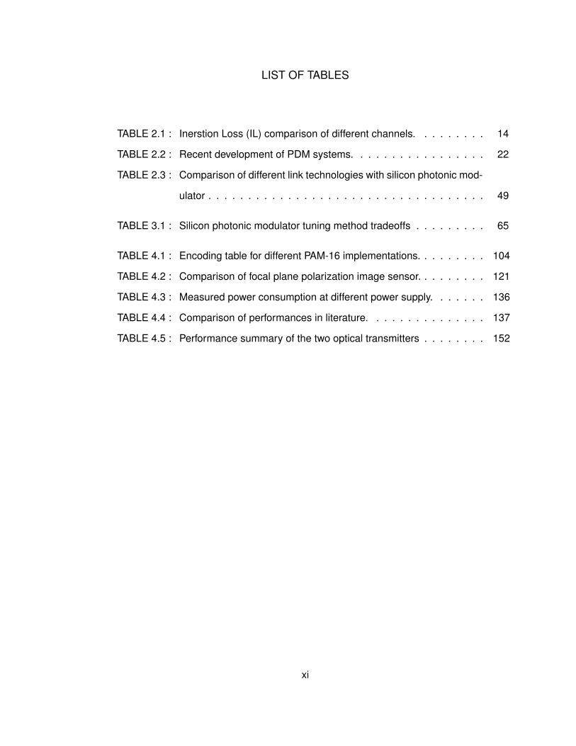
LIST OF TABLES
TABLE 2.1 : Inerstion Loss (IL) comparison of different channels. . . . . . . . . 14
TABLE 2.2 : Recent development of PDM systems. . . . . . . . . . . . . . . . . 22
TABLE 2.3 : Comparison of different link technologies with silicon photonic mod-
ulator . . . . . . . . . . . . . . . . . . . . . . . . . . . . . . . . . . . 49
TABLE 3.1 : Silicon photonic modulator tuning method tradeoffs . . . . . . . . . 65
TABLE 4.1 : Encoding table for different PAM-16 implementations. . . . . . . . . 104
TABLE 4.2 : Comparison of focal plane polarization image sensor. . . . . . . . . 121
TABLE 4.3 : Measured power consumption at different power supply. . . . . . . 136
TABLE 4.4 : Comparison of performances in literature. . . . . . . . . . . . . . . 137
TABLE 4.5 : Performance summary of the two optical transmitters . . . . . . . . 152
xi

LIST OF ILLUSTRATIONS
FIGURE 1.1 : Global IP traffic forcast.(Source: Cisco VNI, 2012) . . . . . . . . 1
FIGURE 2.1 : Moore’s Law of IC (data is compiled from various data sheets and
web sources): (A)CPU Total Transistor Count. (B)CPU Frequency.
(C)GPU Total Transistor Count. (D)FPGA Total Transistor Count. 12
FIGURE 2.2 : IEEE802.3 100Gb/s backplane insertion loss (Data is from IEEE
website). . . . . . . . . . . . . . . . . . . . . . . . . . . . . . . . . 13
FIGURE 2.3 : Causes of copper channel loss: (A) Skin effect. (B) Surface rough-
ness. (C) Dielectric loss . . . . . . . . . . . . . . . . . . . . . . . 14
FIGURE 2.4 : System diagram of a DWDM optical link. . . . . . . . . . . . . . . 19
FIGURE 2.5 : Constellation diagrams of different modulation formats in optical
communications. . . . . . . . . . . . . . . . . . . . . . . . . . . . 21
FIGURE 2.6 : Simulation result of photon shot noise. PI is the number of interac-
tion photons with the photo detector. (A)Distribution when number
of photons that interact with detector is small. (B)Distribution when
number of photons that interact with detector is large. (C)Distribution
with different number of photons that interact with detector. . . . 27
FIGURE 2.7 : Optical Modulator Classification. . . . . . . . . . . . . . . . . . . 32
FIGURE 2.8 : (A)VCSEL cross section. (B)VCSEL output power v.s. bias volt-
age. (C)VCSEL driving diagram. . . . . . . . . . . . . . . . . . . 33
FIGURE 2.9 : Mach-Zehnder interferometer (MZI) modulator working diagram. 35
FIGURE 2.10 :Fabry-Perot modulator (A)Modulator diagram (B)Maximum output
condition (C)Transmittance curve . . . . . . . . . . . . . . . . . . 37
FIGURE 2.11 :(A) Ring resonator modulator diagram. (B)Electric field simulation
of ring modulator. . . . . . . . . . . . . . . . . . . . . . . . . . . . 38
FIGURE 2.12 :Definition of OMA . . . . . . . . . . . . . . . . . . . . . . . . . . . 38
xii

FIGURE 2.13 :Extinction ratio and power efficiency comparison. . . . . . . . . . 40
FIGURE 2.14 :Diagram of light pulse and different types of chirp. . . . . . . . . . 42
FIGURE 2.15 :(A)Cross section of P-i-N silicon modulator. (B)Cross section of
PN junction silicon modulator. (C)Cross section of MOS capacitor
silicon modulator. (D)Cross section of SISCAP silicon modulator. 45
FIGURE 2.16 :Vπ · L comparison chart of different modulator technologies (data
is compiled from various research publications). . . . . . . . . . . 46
FIGURE 2.17 :(A)MZM based on SISCAP (Courtesy of CISCO Systems). (B)Ring
resonator based on forward biased lateral P-i-N diode. . . . . . . 47
FIGURE 3.1 : (A)Diagram of SISCAP based MZM. (B)Cross section of SISCAP
structure (Courtesy of CISCO). . . . . . . . . . . . . . . . . . . . 53
FIGURE 3.2 : SISCAP high frequency capacitance versus applied voltage. . . . 54
FIGURE 3.3 : Output optical power transfer curve in SISCAP MZM. . . . . . . . 56
FIGURE 3.4 : (A)Differential driving of SISCAP MZM. (B)Common-poly driving
of SISCAP MZM. (C)Asymmetric poly driving of SISCAP MZM. . 58
FIGURE 3.5 : SISCAP electrical structure. . . . . . . . . . . . . . . . . . . . . . 62
FIGURE 3.6 : SISCAP band diagram at different bias conditions (not drawn to
scale). (A)V a = VFB. (B)V a > VFB. (C)V a < VFB . . . . . . . . 63
FIGURE 3.7 : SISCAP capacitance. (A)At low frequency. (B)At high frequency. 66
FIGURE 3.8 : SISCAP capacitance break down. (A)In accumulation region. (B)In
depletion region. . . . . . . . . . . . . . . . . . . . . . . . . . . . 67
FIGURE 3.9 : Simulated SISCAP C-V curve with different gate oxide thickness. 68
FIGURE 3.10 :Simulated SISCAP C-V curve at different doping levels. . . . . . 69
FIGURE 3.11 :FDTD electrical domain simulation results in SISCAP. (A)Electric
field (V/cm). (B)Hole concentration (cm−1).(C)Electron concentra-
tion (cm−1). . . . . . . . . . . . . . . . . . . . . . . . . . . . . . . 72
xiii

FIGURE 3.12 :FDTD simulation result of the optical mode (electric field) in SIS-
CAP and MOSCAP. (A)SISCAP with λ = 1310nm. (B)SISCAP
with λ = 1550nm. (C)MOSCAP with λ = 1310nm . . . . . . . . . 74
FIGURE 3.13 :FDTD simulation result of the phase shift in SISCAP. . . . . . . . 75
FIGURE 3.14 :Top level circuit model diagram of the SISCAP based MZI. . . . . 76
FIGURE 3.15 :Model hierarchy created in this research. . . . . . . . . . . . . . 77
FIGURE 3.16 :Optical transfer function in the MZI structure. . . . . . . . . . . . 78
FIGURE 3.17 :Electrical model of SISCAP created in this research. . . . . . . . 82
FIGURE 3.18 :Measured SISCAP capacitance vs voltage and the comparison
with curve fitting result. . . . . . . . . . . . . . . . . . . . . . . . . 82
FIGURE 3.19 :Measurement result and curve fitting comparison. (A)SISCAP at-
tenuation vs voltage. (B)SISCAP phase shift vs voltage. . . . . . 84
FIGURE 3.20 :Transmitter connection diagram. . . . . . . . . . . . . . . . . . . 85
FIGURE 3.21 :Wire bond model. . . . . . . . . . . . . . . . . . . . . . . . . . . . 86
FIGURE 3.22 :Simulation result of the bond wire model. (A)Self inductance and
mutual inductance. (B) Skin depth and resistance for 800µm long
bond wire. (C) Mutual capacitance for different bond wire distance
‘D’. . . . . . . . . . . . . . . . . . . . . . . . . . . . . . . . . . . . 87
FIGURE 3.23 :Simulated eye diagram (on the top) and measured optical eye dia-
gram (on the bottom) at different data rate. (A)10Gb/s. (B)28Gb/s.
. . . . . . . . . . . . . . . . . . . . . . . . . . . . . . . . . . . . . 88
FIGURE 4.1 : System architecture of the proposed optical transmitter. . . . . . . 90
FIGURE 4.2 : Measured SISCAP MZI characters versus MZI length for different
doping levels, center overlap lengths, and contact to center spac-
ings. (A)ER change with MZI arm length. (B)OMA change with
MZI arm length. (C)Average optical output power change with MZI
arm length. . . . . . . . . . . . . . . . . . . . . . . . . . . . . . . 95
xiv

FIGURE 4.3 : Simulated optical eye diagram at 40Gb/s with 480µm SISCAP RF
section. . . . . . . . . . . . . . . . . . . . . . . . . . . . . . . . . 96
FIGURE 4.4 : 1-tap FFE implementation in SISCAP MZM. . . . . . . . . . . . . 97
FIGURE 4.5 : ∆φ change in the MZM. (A)Without traveling wave matching. (B)With
traveling wave matching. . . . . . . . . . . . . . . . . . . . . . . . 97
FIGURE 4.6 : Measured OOK modulation eye diagram from the test chip. (A)32Gb/s
PRBS7 electrical input. (B)32Gb/s PRBS7 optical output. (C)40Gb/s
PRBS31 electrical input. (D)40Gb/s PRBS31 optical output. . . . 98
FIGURE 4.7 : Simplified MZI driver diagram for power consumption analysis. . 100
FIGURE 4.8 : Different PAM schemes. (A)PAM-2(OOK). (B)PAM-4. (C)PAM-16. 102
FIGURE 4.9 : Implementation methods of PAM-16 with segmented SISCAP MZM:
PAM-2 or OOK (top), binary code weighted PAM-16 (middle) and
thermometer code weighted PAM-16 (bottom). . . . . . . . . . . 103
FIGURE 4.10 :(A)Binary/thermometer code weighted PAM-N (N=8 in this plot).
(B)Enhanced binary code weighted PAM-N (N=8 in this plot). . . 105
FIGURE 4.11 :MZM structure implementing the enhanced binary code weighted
PAM-16 scheme. . . . . . . . . . . . . . . . . . . . . . . . . . . . 105
FIGURE 4.12 :PAM-N (N=4 in this plot) level position optimization. (A)Before op-
timization: the 4 levels are unequally spaced. (B)Using 3 SISCAP
segments with random lengths to generate 8 levels. (C)After op-
timization: 4 levels with equal space are pick from (B) to get the
final PAM-4. . . . . . . . . . . . . . . . . . . . . . . . . . . . . . . 106
FIGURE 4.13 :Output intensity distribution in PAM-N. (A)With equally spaced out-
put levels. (B)With optimum output level spacing. . . . . . . . . . 107
FIGURE 4.14 :Simulated PAM-16 optical eye diagram with PRBS31 pattern. (A)Data
rate is 40Gb/s with symbol rate = 10GBaud/s. (B)Data rate is
112Gb/s with symbol rate = 28GBaud/s. . . . . . . . . . . . . . 108
FIGURE 4.15 :Metal wire grid for polarization filter. . . . . . . . . . . . . . . . . 111
xv

FIGURE 4.16 :FDTD simulation model (right) and electrical field (left) of metal
wire grid polarization filter. . . . . . . . . . . . . . . . . . . . . . . 112
FIGURE 4.17 :Simulation results of the extinction ratio for a single layer wire-grid
made of the first metal layer (M1), while (A) wire-grid period Λ is
increasing from 100nm to 180nm with a fixed wire-grid duty cycle
of 50%; (B) the duty cycle of the wire-grid is increasing from 40%
to 80% with a fixed Λ = 200nm. The extinction ratio is evaluated
for different incident wavelength varying from 450nm to 650nm. . 113
FIGURE 4.18 :A comparison of the extinction ratio performance while different
metal layer is selected for a single layer wire-grid implementation. 114
FIGURE 4.19 :Simulation result of metal wire grid polarizer at communication
wave length: ER (top), transmission efficiency T⊥ (middle) and
reflection efficiency R⊥ (bottom). . . . . . . . . . . . . . . . . . . 115
FIGURE 4.20 :(A) Circuit diagram of the overall system. The 32 × 32 active pixel
sensor (APS) array is divided into 2× 2 blocks. Within each block,
three wire-grid polarizer filters are implemented on top of the pho-
todiode region. The architecture of the pixel and current conveyor
is illustrated on the right. (B)Microphotography of the the polariza-
tion image sensor. (C)Layout of the 45 wire grid with an effective
period of about 250nm. . . . . . . . . . . . . . . . . . . . . . . . 117
FIGURE 4.21 :(A)Metal stack of the 65nm CMOS process. (B)Wire grid cross
section. (C)Pixel mosaic structure. . . . . . . . . . . . . . . . . . 118
FIGURE 4.22 :Test setup of the polarization image sensor. . . . . . . . . . . . . 118
FIGURE 4.23 :Measurement result. (A)Transmission efficiency. (B)Phase error
of pixels covered by wire-grid with a different layout orientations
of 0, 45 and 90. The degree value on the x-axis is the rotation
angle of the polarizer on the path of the incident. . . . . . . . . . 120
FIGURE 4.24 :Sample image of the polarization image sensor. . . . . . . . . . . 121
xvi

FIGURE 4.25 :Top level circuit diagram of the transmitter. . . . . . . . . . . . . . 123
FIGURE 4.26 :DLL based Frequency doubler. . . . . . . . . . . . . . . . . . . . 125
FIGURE 4.27 :Simulation of 40nm process inverter chain at 1.0V supply. (A)Testbench.
(B)Waveform for SS process, -40C. . . . . . . . . . . . . . . . . 126
FIGURE 4.28 :(A) SEM photo of the AlN CMR and the MBVD circuit model of the
resonator, (B) Measured AlN CMR admittance curve. . . . . . . . 130
FIGURE 4.29 :Schematic of the tunable Pierce oscillator working in sub-threshold
region. . . . . . . . . . . . . . . . . . . . . . . . . . . . . . . . . . 131
FIGURE 4.30 :(A) Simulated transient waveform of the oscillator. (B) Simulated
frequency tuning range. . . . . . . . . . . . . . . . . . . . . . . . 133
FIGURE 4.31 :Photo of the oscillator system (Left: Electrical IC, Right: MEMS
resonator). . . . . . . . . . . . . . . . . . . . . . . . . . . . . . . 134
FIGURE 4.32 :Characterization result with 3 different resonators: 204MHz(Top),
517MHz(Middle) and 850MHz(Bottom). (A)Measured output fre-
quency. (B)Measured frequency variation. . . . . . . . . . . . . . 135
FIGURE 4.33 :Measured phase noise of the 204MHz oscillator. . . . . . . . . . 137
FIGURE 4.34 :Master-slave CDR top level diagram. . . . . . . . . . . . . . . . . 138
FIGURE 4.35 :Half rate bang-bang CDR timing diagram. . . . . . . . . . . . . . 139
FIGURE 4.36 :Phase detector design: using CML logic (top) and using CMOS
logic (bottom). . . . . . . . . . . . . . . . . . . . . . . . . . . . . . 140
FIGURE 4.37 :Dynamic D flip-flop built with transmission gate inverter. . . . . . 141
FIGURE 4.38 :Circuit diagram of the phase interpolator. . . . . . . . . . . . . . 142
FIGURE 4.39 :Phase interpolator’s output with different input waveform. Bold red
curve is input IP . Bold green curve is input QP . Thin blue curve
is the output signal after interpolation. . . . . . . . . . . . . . . . 143
FIGURE 4.40 :Clock buffer and duty cycle correction. . . . . . . . . . . . . . . . 143
FIGURE 4.41 :(A)Simulated phase step. (B)DNL of phase step. . . . . . . . . . 144
xvii

FIGURE 4.42 :Chip photograph of the 40Gb/s serial (OOK) optical transmitter:
electrical driver IC (top) in 40nm CMOS and optical modulator IC
in 0.13µm SOI CMOS (bottom). . . . . . . . . . . . . . . . . . . . 145
FIGURE 4.43 :Measurement setup of the optical transmitter for both 40G/s serial
and PAM-16 operation. . . . . . . . . . . . . . . . . . . . . . . . . 146
FIGURE 4.44 :A close look of the setup in the DUT region. . . . . . . . . . . . . 147
FIGURE 4.45 :Measured OOK modulation eye diagram showing 20Gb/swith large
duty-cycle distortion. . . . . . . . . . . . . . . . . . . . . . . . . . 148
FIGURE 4.46 :Measured PAM-4 modulation eye diagram . (A)Without average in
the scope settings. (B)With average in the scope settings. . . . . 149
FIGURE 4.47 :Measured PAM-16 modulation eye diagram. (A)DC level sweep.
(B)Running at 40Gb/s with bit errors due to eye closure. . . . . . 150
FIGURE 4.48 :ER measurement result of the PAM-16 transmitter. . . . . . . . . 151
xviii

CHAPTER 1 : Introduction
Wireline interconnects, as a medium of conveying information, exist in every scale of peo-
ple’s daily lives. On the macro level, the inter-continental IP network has greatly influenced
the way of how people communicate, work and entertain. On the micro level, the nanome-
ter wide metal wire inside a modern integrated circuits is an essential element responsible
for transmitting and receiving signals among transistors.
2010 2011 2012 2013 2014 2015 2016
Business 47,160 59,304 91,356 112,500 134,724 157,560 91,356
Consumer 194,652 309,504 446,928 566,376 715,824 913,236 1,165,82
0
200,000
400,000
600,000
800,000
1,000,000
1,200,000
1,400,000
Traf
fic(
Pe
taB
yte
s)
Annual Global IP Traffic Forcast
Figure 1.1: Global IP traffic forcast.(Source: Cisco VNI, 2012)
Despite of the economy contracting since 2008, the network traffic as shown in Figure 1.1,
driven by streaming video and other data intensive applications such as cloud computing
has been steadily increasing and is expected to reach 110.3 exa-bytes per month or nearly
1.3 zetta-byte (1.3 × 10²¹ Bytes) per year by the end of 2016 [1], which is equivalent to a
compound annual growth rate of 29%. The demand mostly comes from consumer traffic
which will, in 2016, account for more than 90% of all internet traffic because of the widely
use of mobile devices such as smart phone and tablet computers.
1

Thirst for bandwidth also exists in the supercomputers and data centers driven by cus-
tomers from financial services, technical companies and military. One major barrier to take
supercomputing to the next level are limitations on data transmission rates between CPUs
and memory, and the connections that switch between CPU nodes for parallel process-
ing. Supercomputer’s tremendous speed is achieved through “parallel processing” which
allows thousands of CPUs to work in concert through a series of switches. The current
design of supercomputers requires significant cabling to tie together inter-node links using
materials that are inefficient, resulting in high energy requirements and high costs for the
operation. Statistics shows that almost 15% ∼ 23% of energy is consumed by the inter-
connects [2]. Existing supercomputer such as Roadrunner [3] has a significant appetite
for power, consuming roughly three megawatts of power, or about the power required by a
large suburban shopping center. The power needs for a Japanese supercomputer devel-
oped by Fujitsu Labs is in the neighborhood of 13 megawatts [4], which would likely require
its own power station.
Similarly, seeking for higher speed is the ultimate goal for the semiconductor industry be-
cause of the increasingly demand on computational power. Benefit from the semiconductor
processing scaling down, the total transistor count as well as the overall chip performance
of today’s computer processors follows pretty well Moore’s law. However, this trend does
not apply to the maximum clock frequency a processor can operate mainly because of
the on-chip interconnect delays introduced by the parasitic R and C. It is more likely that
the chip speed will be limited by the wire delay instead of the transistor’s transit frequency
fT which is generally higher for finer process nodes. This speed gap is one of the major
issues for further improving the performance of processors.
Traditionally, the medium for long distance data communication is dominated by optical
fiber because of its high speed, low loss, and excellent signal integrity. However, high
power consumption, low link density and high cost seriously prevent traditional optical
transceiver from being the next generation of optical link technology for novel applications.
2

For short reach applications, although copper is the most cost-effective choice for intercon-
nect, the issues related to the existing electrical links such as high power, low bandwidth
and cross talk become major bottlenecks for the next generation of High Performance
Computing (HPC).
As the communication bandwidth requirement increases at its current exponential rate,
copper and traditional optoelectronics interconnects currently provide these connections
are hitting a wall in terms of power consumption, signal integrity and cost limitations at
high speeds. Both applications are seeking for an innovative solution of link technology to
tackle those current issues.
Compared to other emerging or novel interconnect technologies such wireless, nanowire,
Single-Walled Carbon Nanotube (SWCNT) and superconductor, optical is still the best
candidate with a foreseeable future to meet both the performance and commercialization
standard. There is already a tendency of replacing copper wires with optical links in all
system levels even for the IC’s on-chip interconnection [5].
Among all building blocks, finding better method for controlling light is the key element to
build the optical link which has drawn extensive research attention for the past 60 years
since the invention of the laser [6]. In order to address the current issues related to the
optical and electrical links and target the next generation of supercomputers and data
communication, we propose to develop a high performance optical transmitter by utilizing
CISCO R©’s proprietary CMOS photonic technology. The research would seek to achieve
the following outcomes:
1. Reduction of power consumption due to optical interconnects to less than 5pJ/bit
without the need for ring resonator modulators and less than 300fJ/bit for short
distance data bus applications.
2. Enable the increase in performance (computing speed) from Peta-Flop to Exa-Flops
without the proportional increase in cost or power consumption that would be pro-
3

hibitive to next generation system architectures by means of increasing the maximum
data transmission rate over a single fiber. The goal is to achieve 40Gb/s transmission
data rate using single fiber and single wavelength without using Dense Wavelength
Division Multiplexing (DWDM).
3. Explore the advanced modulation scheme such as PAM-16 to increase the spectrum
efficiency while keeping the same or less power figure.
However, realizing these targets is not trivial. It requires significant research and develop-
ment efforts with heavily investment on equipment, software and human resource. A group
of people at Lightwire (currently CISCO) have been actively involved in this development
process for more than 10 years. This research, as a part of this large project, will focus
on the improvement of both electrical IC and optical IC for the optical transmitter based on
their existing work. An accurate circuit model of the optical device is created to speed up
the performance optimization and enable co-simulation of electrical driver. Circuit architec-
tures and sub blocks are chosen to minimized the power consumption without sacrificing
the speed and noise immunity.
Major challenges of this research are:
1. How to precisely model the behaviors of the electrical IC and optical IC to optimize
their performance.
2. How to push the speed limit of current CMOS technology higher to the 40Gb/s range.
3. How to keep the power figure low with the presence of various leakage sources and
routing parasitics.
4. How to deal with non-ideal factors such as supply noise and signal interference.
None of them are trivial for circuits running above 10GHz. Efforts have been made to
resolve these issues and will be discussed in detail in the corresponding chapters.
4

As a result, a silicon photonic based optical transmitter employing 1V supply, featuring
20Gb/s data rate is fabricated. The system consists of an electrical driver in 40nm CMOS
and an optical MZI (Mach-Zehnder Interferometer) modulator with an RF length of less than
0.5mm in 0.13µm SOI CMOS. Two modulation schemes are successfully demonstrated:
OOK (On-Off Keying) and Pulse-Amplitude-Modulation-N (PAM-N N=4, 16). Both versions
demonstrate signal integrity, interface density, and scalability that fit into the next generation
data communication and exa-scale computing. Modulation power at 20Gb/s data rate for
OOK and PAM-16 of 4pJ/bit and 0.25pJ/bit are achieved for the first time of an MZI type
optical modulator, respectively.
The contribution of this thesis is summarized as follows:
1. Enhance the existing model of the optical device from Lightwire by adding more accu-
rate parasitic R, L, C information such as bond wire’s mutual inductance, skin effect,
and S-parameter model of the routing. Besides the parasitic components, the model
also incorporates the voltage and temperature dependency. Geometry dependent
information is also added which means the final model is almost fully parameterized.
Thus, the user can simply set the size, doping, voltage, and etc to get the device’s
performance simulated.
2. MZI(Mach-Zehnder Interferometer) models for advanced modulation scheme have
been created including 5 different versions: 40Gb/s serial, PAM-16 binary weighted,
PAM-16 thermometer weighted, PAM-16 enhanced binary weighted, and PAM-16
enhanced thermometer weighted. Other designers can use these models to optimize
the MZI length and determine the best scheme to be implemented.
3. Electrical circuits supporting the operation of the MZI have been developed which
are: 1) Phase picking CDR(clock and data recovery); 2) Resistive termination with
adjustable range and automatic calibration circuit to compensate for PVT variation;
3) Various sense and control blocks such as laser driver, voltage sensor and temper-
5

ature sensor which are migrated from different process based on existing Lightwire’s
designs.
4. Matlab model of CDR is created and simulated to evaluating the jitter tolerance per-
formance. The jitter budget analysis is then carried out to help selecting the structure
of the CDR.
5. A MEMS(Micro-Electro-Mechanical Systems) based tunable oscillator is designed to
explore the possibility of further reducing the power consumption.
6. Explore the possibility of using the on-chip metal wire grid to detect the polarization
status of light. An image sensor integrated with focal plane 2 × 2 wire-grid polarizer
filter mosaic targeted at visible spectrum is designed.
The thesis comprises 5 chapters. Chapter 2 starts with an general overview of the high
speed interconnects. The advantages and issues with existing technologies are briefly
compared. The remaining sections will focus on the optical interconnect, covering the
both the system level structure and key building blocks. The fundamental properties of
light and its interactions with materials such as electro-absorptive effect, electro-optical
effect and free carrier effect, are described first. The classification and key parameters to
characterize the optical modulator is then discussed in detail. Finally, the optical modulator
based on silicon photonic technology is introduced. Various modulator structures, such
as ring resonator, PN junction based MZI, PIN based MZI , and SISCAP based MZI are
presented in detail. Finally, the chapter will conclude with the performance comparison of
different modulator architectures.
Chapter 3 first introduces basic the structure and key parameters of the SISCAP structure.
A simplified analytical model is then created and discussed. More accurate numerical
simulation is performed and result is given. Based on the model and lab characterization,
a circuit model is constructed which enable the co-simulation of SISCAP with the electrical
driver.
6

Chapter 4 is devoted to the performance optimization of the SISCAP based MZI transmit-
ter. The research focuses on the improvement both the electrical IC and optical IC. The
techniques to reduce the power as well as increase the operating speed are discussed in
detail from the system level down to each building blocks. Simulation result and measure-
ment data are then presented and discussed.
An overall summary of this dissertation is provided in Chapter 5. Suggestions for future
research directions are given in the end.
7

CHAPTER 2 : High Speed Interconnect Overview
This chapter first introduces the background of different interconnect technologies with
more emphasis on the optical links. Among all the building blocks in an optical communi-
cation link, the transmitter especially the optical modulator serves a more important role.
The rest of this chapter concentrates on the optical transmitter technology, starting by in-
troducing the fundamental properties of light. Then, the interaction of materials with light
will be described in detail which serves as the basis of most of the optical modulators. Nex-
t, a classification of optical modulators will be given followed by the major parameters to
characterize the performance of the modulator. Last but not least, the silicon based optical
modulators will be presented. The key parameters of different modulators are summarized
in the end of this chapter.
2.1. Interconnect at a Glance
Communication, coming from the Latin word “communis” which means to share, is the
activity of exchanging information, messages, or thoughts and exists in every aspects of
our society [7]. Interconnect, as the medium of communication, enables the convey of
information by various means such as sound, visuals, or optics/electric signals etc. The
developments of interconnect technologies make possible the communication from billions
of miles between the the earth and the satellite “Voyager1” [8] down to tens of nanometers
between two transistors in the latest generation of computer processor [9].
Theoretically, any detectable changes can be used to carry information. Thus, intercon-
nection can be realized in various approaches. It could be the mechanical vibration of air
stimulated by human’s speech where the combinations of pitches and intensity represent
different meanings. It could be the beacon out of a lighthouse where colors, intensity and
on/off interval provide important information, such as weather conditions, reef locations
and status of an airport. It could be the electrical signals going either wirelessly in the air
or through a copper cable. It could be a Fedex truck loaded with thousands of hard drives
8

full of data travelling at 60mph on the highway which may have more bandwidth than most
of our home networks. It could also be the quantum status of an atom travelling faster than
light in the teleportation [10] predicted by Albert Einstein’s theory of special relativity [11].
Among all the realizations of interconnects, three of them are most widely adopted by
modern information systems for different applications:
1. Wireless signals via the air
2. Electrical signals carried by metal wire
3. Optical signals through fiber
The choice of which technique to implement is determined by the systems’ unique char-
acteristics which lead to trade-offs among speed, distance, power, cost and deployment
difficulty, just to name a few.
2.1.1. Wireless Interconnect
Wireless interconnect is undoubtedly the first choice for applications where mobility is im-
portant such as in the cell phone market, or when it is impossible to establish a wired
connection such as in communications between the earth and satellite. Beside the con-
venience that user device can move easily within the signal range, wireless also has the
advantages of easy and inexpensive to deploy since there is no need for cabling infras-
tructures and devices. In addition, it can easily support hundreds of users simultaneously
through either broadcasting or multiplexing.
However, wireless has its own disadvantages such as relatively lower bandwidth, limited
working ranges affected by environment condition, and less security. Due to attenuation
and interference, the wireless link can not support very high data rate. Even the latest
802.11ac WiFi standard [12] can only reach 867Mb/s within tens of meter using a single
antenna. Going to higher carrier frequencies such as 60GHz can provide more bandwidth
but the distance is significantly reduced due to attenuation. With the evolution of mobile
9

network from GSM to 3G or 4G LTE, the global mobile phone sales reached 472 million
units in the fourth quarter of 2012 [13], 44% of which are smart phones with data network
feature. In order to support the explosive network traffic, the backbone system in the base
station has to use electrical routers/switches and optical links running at multiple Gb/s.
Attenuation is a serious problem in extending the wireless link’s range. Apart from the
intensity decrease due to inverse-square law geometric spreading, the energy of electro-
magnetic wave can be absorbed or scattered by the molecules in the atmosphere. The
wireless signals are also vulnerable to a wide variety of interference, as well as complex
propagation effects which degrades the signal to noise ratio (SNR) and finally reduce the
link distance. Increasing the transmit power, adding repeaters or using a directional an-
tenna can partially address this issue at the expense of decreased power efficiency and
increased system cost. Wireless networks is also prone to breaches due to the physical
channel’s open nature. Utilizing the encryption technologies can only alleviate this issue
but doesn’t guarantee 100% level of security.
2.1.2. Electrical Wireline Interconnect
Compared to wireless and all the other forms of communication mediums, metal wire is
still the most widely adopted medium for a broad range of applications because it has
the advantages of simple interface, wide selections of link distance, flexible data rate, low
power and inexpensive to fabricate. Since most of today’s information and data are pro-
cessed electrically by electrical integrated circuit (IC), metal wire carrying electrical signals
eliminating the need of doing signal converting at systems’ boundaries which makes the
interface between different functional blocks very simple. While considering the distance
of a wired link, it can be tens of nanometers in a semiconductor chip or several kilometers
in the metropolitan networks. Besides, almost all the circuit board level connections, rack
to rack links and local area networks (LAN) are implemented with copper wires. As for link
capacity, a single channel of metal wire provides flexible choices from several hundred bit/s
to tens of Gb/s depending on distance. The link capacity can also be easily expanded by
10

running multiple channels in parallel. Copper wire also consumes less energy than wire-
less since most of its signal power is confined within the wire and sent only to the receivers
with known distance and data rate. As regards the cost, since both the material is easy to
acquire and the manufacturing process is mature, metal wires can be fabricated in large
volume at very low price. Electrical wiring can also carry power and provide ground which
are essential to any electronic circuits.
Albeit having those advantages, metal wires still suffer from several drawbacks which pre-
vent them from meeting the future needs of interconnect. These channel impairments
include but are not limited to:
1. Limited bandwidth and large delay caused by parasitic RC
2. Frequency dependent attenuation (insertion loss) which results in inter-symbol inter-
ference(ISI) and finally leads to deterministic jitter (TX and RX)
3. Crosstalk caused by coupling between traces and in connector which includes near
end crosstalk (NEXT) and far end crosstalk (FEXT)
4. Reflection(return loss) caused by impedance discontinuities
5. Thermal noise which degrades the SNR
First, the metal wire demonstrates parasitic R and C which limit the maximum achievable
signal frequency and increase the signal latency especially in the IC industry. Fueled by
process scaling during the past 50 years, the number of transistors in a processor and
its overall computational power double every two years which is known as Moore’s Law.
Although the scaling predicted by Moore’s Law will eventually hit a wall when the thickness
of transistor’s gate oxide reaches 0.5nm (about 2 times of silicon atom’s diameter) as
indicated by ITRS 2006 Front End Process Update [14], a quick check among different
computer companies shows the total transistor count in modern CPU, GPU, and FPGA
still follows the law pretty closely so far (Figure 2.1 (A), (C) and (D)).
11

As Moore’s Law applies to the total transistor count, it is not the case for the maximum clock
frequency although the transistor performance, such as intrinsic frequency (fT ), improves
as gate length, dielectric thickness, and junction depth are scaled. From Figure 2.1 (B), it is
clear to see that the maximum CPU frequency deviates from Moore’s Law after 2000. The
key reason of this deviation is that the metal wires in modern integrated circuits, usually
made of copper or aluminum, don’t benefit from the scaling since the parasitic R and C,
intrinsic to those wires, increase as the minimum feature size decreases. Parasitic RC from
interconnect contributes most of the delays not only limiting the local switching frequency
but also increase the global signal latency. Simulations indicates that for 65nm process,
the signal delay of 0.1mm copper trace is about 200ps, about two orders of magnitude
higher than the propagation delay of the electromagnetic waves associated with SiO2.
1980 1990 2000 2010
4
5
6
7
8
9
Year
Tra
nsis
tor
Cou
nt (
log
scal
e)
CPU Transistor Count and Moore’s Law
1980 1990 2000 20105
6
7
8
9
10
11
Year
CP
U C
lock
Fre
quen
cy (
log
scal
e)
CPU Frequency and Moore’s Law
(A) (B)
1998 2000 2002 2004 2006 2008 2010 2012
7
7.5
8
8.5
9
9.5
Year
Tra
nsis
tor
Cou
nt (
log
scal
e)
GPU Transistor Count and Moore’s Law
1998 2000 2002 2004 2006 2008 2010
8
8.5
9
9.5
Year
Tra
nsis
tor
Cou
nt (
log
scal
e)
FPGA Transistor Count and Moore’s Law
(C) (D)Figure 2.1: Moore’s Law of IC (data is compiled from various data sheets and websources): (A)CPU Total Transistor Count. (B)CPU Frequency. (C)GPU Total TransistorCount. (D)FPGA Total Transistor Count.
Thus, the RC delay is worse in finer technology with thinner and narrower wires which is
a serious issue for higher operating frequency and affects the overall chip performance.
12

While the resistivity can be reduced by replacing aluminum with copper, tremendous re-
search efforts have focused primarily on how to minimize the parasitic capacitance. One
method is to use low dielectric constant (low-k) material such as fluorine-doped silicon
dioxide [15] or carbon-doped silicon dioxide [16] which lowers the dielectric constant of
SiO2 from 3.9 to 3.0. Researchers also try to partially remove the SiO2 between metals
which creates voids or pores filled with air with a dielectric constant of nearly 1. Employing
this method, the effective dielectric constant as low as 2.0 has been reported [17]. More-
over, the power consumption is higher with larger parasitic. As IC process scales down,
the energy consumed by the interconnect eventually exceeds that is needed to switch a
transistor on and off. Simulation result shows, for 40nm process, the energies to make a
’0’ to ’1’ transition in a transistor and a 1mm wire are 0.15fJ and 3.5fJ , respectively.
The second issue of metal wire is it has a frequency dependent loss.
0 10 20 30 40-200
-150
-100
-50
0
Loss
(dB
)
Frequency(GHz)
Frequency Dependent Insertion Loss
Nelco4000-6 42.8"Megtron-6 42.8"Nelco4000-6 29.8"Megtron-6 29.8"
Figure 2.2: IEEE802.3 100Gb/s backplane insertion loss (Data is from IEEE website).
Figure 2.2 plots the insertion loss versus signal frequency of a typical IEEE802.3 100Gb/s
backplane with different substrate materials and trace lengths [18]. The insertion losses at
10GHz and 20GHz are summarized in Table 2.1 which shows, at 20-40Gb/s, the electrical
13

Table 2.1: Inerstion Loss (IL) comparison of different channels.Channel Type Length(inch) IL at 10GHz(dB) IL at 20GHz(dB)Nelco4000-6 42.8¨ -39.9 -79.3Megtron-6 42.8¨ -22.6 -43.3Nelco4000-6 29.8¨ -28.1 -57.2Megtron-6 29.8¨ -16.2 -32.2
backplane may have huge insertion loss which could exceed 80dB at half of the signal data
rate. In effect, this frequency dependent loss tends to attenuate signal with high frequency
pattern such as 01010101 more than the low frequency pattern such as 111000111 and
leads to ISI or Data-Dependent Jitter which limits the range of communication.
There are 3 major causes of insertion loss in the copper channel:
1. Skin effect (IL(dB) ∝√Frequency)
2. Surface roughness (IL(dB) ∝ Frequency)
3. Dielectric loss (IL(dB) ∝ Frequency)
as denoted in Figure 2.3.
Metal
MetalDepth
AC Current Density
f1>f2
Metal
(A) (B) (C)
Figure 2.3: Causes of copper channel loss: (A) Skin effect. (B) Surface roughness. (C)Dielectric loss
Skin effect confines the high frequency AC current to flow only in a thin layer on the metal
surface which increases the effective resistance of the channel. The surface roughness
exaggerates the skin effect by increasing the total signal path’s length. The molecules of
the dielectric material usually have more or less the dipole moments due to asymmetric
distributions of positive and negative charges of various atoms. Energy consumed by
14

rotating these dipoles dominates the loss at higher frequency since it is proportional to the
signal frequency.
To address the loss issue, equalization technique, at both the transmitter and the receiver
side, has been employed intensively which tries to compensate the signal distortion of
the communication channel by making the overall frequency response as flat as possible.
Nevertheless, these techniques are still facing a lot of challenges such as high power
consumption, increased chip area, cost and complexity, susceptible to process, voltage,
and temperature (PVT) variations in an analog equalizer, and stringent timing requirements
in a digital equalizer etc.
Another approach to tackle the loss issue is to reduce the symbol rate by implementing
a multi-level modulation scheme such as PAM-4(Pulse-amplitude modulation with 4 lev-
els) [19] where the symbol rate is only one half of the data rate. While PAM-N (N is the
number of levels) achieves a symbol rate reduction of log2N from the data rate, it has the
drawbacks of requiring an log2N -bit DAC (digital-to-analog converter) and an log2N -bit AD-
C (analog-to-digital converter) on both sides of the interconnect as well as reduced SNR
performance. The symbol rate can also be kept low by running multiple wires in parallel.
However, it is difficult to align the parallel data to clock at high frequency due to mismatch.
Furthermore, when integrating so many transceiver into a small area, the heat generated
by these circuitry could be prohibitively high for the system to function properly.
While the use of parallel wires for data and address could mitigate the loss problem and
increases the link capacity to a certain extent, the crosstalk arises from the parasitic capac-
itance between wires which is another severe issue of metal interconnect. Crosstalk not
only increases the chance of data error but also consumes more power while charging and
discharging the parasitic capacitance. To maintain the signal integrity, differential signaling
or shielded wire are widely used while both of them will reduce the link density and incur
higher costs.
15

2.1.3. Optical Interconnect
When an electrical channel is reaching its fundamental limits such as bandwidth and dis-
tance, optical links, on the other hand, are far from those limits. Optical fiber communica-
tion has several major advantages over conventional electrical links.
1. Very long link distance and extreme high data rate
2. Thinner,lighter and low cost
3. No crosstalk issue
An optical link can be treated as a wireless channel with carrier frequency many thousand-
s of times higher than those of microwave electrical carriers (about 194THz for 1.55µm
wavelength) which provides ample bandwidth for data. With the help of wavelength-division
multiplexing (WDM), the optical equivalent of frequency-division multiplexing, one opti-
cal fiber can transmit multiple carriers simultaneously. In addition, advanced modulation
schemes such as pulse amplitude modulation (PAM), quadrature phase-shift keying (QP-
SK), and polarization-division multiplexing further increase the link capacity. Link speed
of 112Tb/s over a 76.8km 7-core fiber has been achieved with 160 107Gb/s channels per
fiber [20]. As transmission technology advances, higher bandwidths are possible over
the same optical fibre links without having to replace the cables. Thanks to the extremely
low loss fiber and low noise optical amplifier, the optical signal can be transmitted over
12,000km at 495Gb/s [21]. The optical fiber core, usually made of SiO2 or glass with a
diameter of 125µm, is cheaper and lighter than copper. More importantly, optical fibre is
immune to electro-magnetic interference due to the dielectric nature of the fiber materials,
and so is ideal for environments where there is high voltage equipment nearby.
Even though an optical link provides unsurpassable link speed and distance over electrical
link, its disadvantages should also be mentioned:
1. Price - Although the raw material for fabricating optical fibres is abundant and cheap,
16

optical links, when considering the transmitter, receiver, repeater, and etc., are still
more expensive than copper. The commercial product are also bulky and power
hungry in order to meet the stringent specifications of the telecom market.
2. Fragility - Optical fibre can’t be bent too much otherwise it will break.
3. Sensitive to chemicals - SiO2 property can be affected by various chemicals such as
hydrogen gas in underwater environment.
4. Opaqueness - Most fibers become hard and opaque when exposed to Nuclear radi-
ation.
5. Hard to maintain - Optical fibres cannot be connected together as a easily as copper
wire.
For these reasons, optical links are mostly found in long haul applications where capacity
and distance were big concerns prior to 2000.
In summary, the choice among wireless, electrical, optical fiber or other technologies for a
particular system is based on a number of trade-offs. There is no single solution can serve
all applications needs.
2.2. Optical Communication Overview
Optical communication has a long history which can go back to more than 2000 years ago.
At that time, people in ancient China, Greece and Egypt once used mechanical methods
to modulate the light including smoke signals, fire beacons, and optical telegraphs [22]
some of which are still being used today in some emergency situations. These approach-
es, which are referred to as free-space optical communication now, can not achieve a very
high data rate due to its mechanical nature. The distance is also subject to environmental
conditions such as fog, rain and day light. Lacking of techniques to tackle these issues,
their positions in real time, long distance communication were soon replaced by electrical
wireline and wireless systems in the latter half of the eighteenth century and early twen-
17

tieth century , during which period extraordinary scientific progresses had been made in
the electromagnetic theory, generation and detection of radio signals, new materials, and
elemental electronic devices etc.
Due to lack of capable technologies to generate, modulate, and detect the the light, the
evolution of optical communication seems to stop until the 1950s. In 1958, the major
breakthrough of optical communication, laser, was first invented [6] after its theoretical
foundations being established by Albert Einstein almost 40 years before [23]. After that,
optical communication embraced its golden age with the explosive discoveries and ad-
vancements in the areas of light sources, light detectors, material’s interaction with light,
low loss optical transmission medium, integrated circuits and etc.
Shortly after the invention of the laser, the semiconductor laser diode was successfully
demonstrated [24] followed by the high speed avalanche photo detector [25]. In the mean
time, extensive research had been carried out to study the material electro-optic proper-
ties which can be potentially used to modulate light. In fact, the first optical modulators
based on electro-optic effect was introduced almost the same time as the ruby laser was
invented [26]. For the optical fiber, the major medium in optical links, the fiber loss has
been reduced from the early date of 20dB/km [27] to about 0.15dB/km [28] at the low-
loss window around 1.55µm. In addition, to compensate for the fiber loss, Erbium-doped
fiber amplifier (EDFA) was invented [29] which greatly extended the optical link reach. Ad-
vanced modulation and multiplexing schemes, such as QAM, DWDM, OFDM (orthogonal
frequency-division multiplexing), and PolPSK (polarization multiplexing phase-shift keying),
have been developed to sustain the increasing demand for bandwidth.
After almost 60 years of intensive developments, a global optical network infrastructure
has been established responsible for carrying virtually all telephone calls and internet traf-
fics. Initially, fiber networks were mainly deployed for long-haul or submarine transmission
because it offers unparallel reach and bandwidth product. In the mean time, the explosive
increasing in network traffic continuously pushes the optical network to the metro level or
18

even into individual homes. For short reach applications such as HPC, there is also a trend
of replacing the interconnect, historically dominated by copper wire, with optical links at all
levels from local area network (LAN) and rack to rack, to board level or even inter chip
interconnect [5]. In these domains, traditional optoelectronics interconnects have some
serious issues in terms of power consumption, link density and cost. For example, the IBM
Roadrunner supercomputer has 57 miles of cable and consumes nearly 3 megawatts of
power, almost 15% ∼23% of which is contributed by the interconnects [2]. The existing
optical transceiver module is also bulky and expensive which usually costs a few thousand
dollars for a 10Gb/s module. To meet the future needs of HPC, the price of optical link has
to be cheaper than $1/Gb/s and the power efficiency has to be better than 5mW/Gb/s [30].
It also needs to be compact such that hundreds of links can fit into a small space.
2.2.1. System Architecture
When people talk about optical communication, most of them refer to the long-haul fiber
network which spreads globally. To increase the capacity, dense wavelength division mul-
tiplexing (DWDM) is intensively employed in today’s optical links, in which more than a
hundred wavelengths carrying 10Gb/s or more data are combined into a single fiber of
125µm in diameter [20, 31, 32].
Laser λ1 Modulator
MUX
Laser λn Modulator
Fiber
Amplifier
Information
Information
DEMUX
Detector λ1
Detector λn
Figure 2.4: System diagram of a DWDM optical link.
Figure 2.4 shows the system diagram of a typical DWDM optical link. In this system, digital
information such as audio, video and data is first converted to optical power through the
external modulator which is known as electrical to optical converter, or E/O converter. The
optical input of the modulator comes from laser sources with different wavelengths (e.g.
λ1 − λn) usually spaced 100GHz or 50GHz away. The laser source could also be directly
19

modulated by the information to generate the desired output. All the outputs from the mod-
ulator are then merged into a single strand of fiber via the optical multiplexer (MUX). After
the light travels a long distance in the fiber, it may suffer from loss, chromatic dispersion
and polarization mode dispersion which require optical amplifier or repeater to regenerate
the signal before it reaches the receiver. On the receiver end, after de-multiplexing (DE-
MUX), lights with different wavelengths are sensed by the photo detector and converted
back to electrical signal (optical to electrical conversion, or O/E). This electrical signal is
then processed, which may include reconditioning the signal in the analog domain and
restoring the clock in the digital domain, to recover the original information.
One of the key building blocks in the optical link is the modulator or the transmitter since it
directly impacts the performance of the link such as capacity, reach, power consumption,
receiver design, and in some applications the cost. In the past 60 years, tremendous
research efforts have been spent in the areas of material, electrical circuit, and fabrication
process etc. to develop the E/O converter in order to meet these performance requests.
The focus of this work is to design a high performance optical transmitter by leveraging the
novel modulator technologies developed by CISCO Systems.
In real systems, there are also other additional blocks to make the link more robust. For
example, a temperature control unit is required for the laser source to keep the wavelength
stable especially in the DWDM system where the channel spacing is so small (0.8nm with
100GHz channel spacing). In the polarization division multiplexing DWDM, a polarization
detector is necessary to de-multiplex the signal. Also, when the optical power exceeds the
working range of the detector, a variable optical attenuator (VOA) is needed.
Although optical links other than this long-haul network may have slightly different topolo-
gies, their fundamental building blocks and system scheme, as mentioned above, are es-
sentially the same.
20

2.2.2. Modulation Format and Spectral Efficiency
Analogous to electrical wireline or wireless communication, the physical signals in opti-
cal communication could have multiple forms. Although continuously changing intensity
of light can carry information such as TV signal [33], it is susceptible to noise, nonlin-
earity of fiber and other non-ideal factors due to its analog nature and is rarely used in
commercial products. On the contrary, digital modulation formats don’t demonstrate these
drawbacks because they map information into discrete digital status. Thus, digital modula-
tion formats are the primary choices in fiber links. The constellation diagrams of different
digital modulation formats are illustrated in Figure 2.5. On-off keying (OOK), as a two-level
ImEx
ReEx
OOK
ImEx
ReEx
DPSK
ImEx
ReEx
PAM-4
ImEx
ReEx
QAM-16
ImEx
ReEx
ImEy
ReEy
PDM-QPSK
ImEx
ReEx
QPSK
Figure 2.5: Constellation diagrams of different modulation formats in optical communica-tions.
amplitude-shift keying (ASK), is probably the simplest form in optical links where the binary
information is represented by the presence and absence of light which can be expressed
by the amplitude of the electric field (Ex) or light intensity (∝ Ex2). Owing to its simplicity,
OOK was exclusively adopted by digital optical networks prior the year of 2000. It is ac-
tually the first format being employed in 40Gb/s commercial product [34] and in 100Gb/s
research project [35]. OOK has a spectral efficiency (SE) of 1 b/s/Hz. To increase the SE,
digital message is encoded to multiple intensity levels resulting in N-level pulse-amplitude
modulation (PAM-N). In a PAM-N link, the SE becomes log2N b/s/Hz where N is the
21

number of levels.
Phase-shift keying (PSK), in which digital signals are mapped to different phases of the
carrier — light, is another important modulation form in optical links. Several schemes
exist for PSK such as binary phase-shift keying (BPSK) — the basic 2-level PSK, differen-
tial phase-shift keying (DPSK) — the differential version of BPSK, quadrature phase-shift
keying (QPSK) — BPSK in quadrature form, and n-PSK — multi-level PSK. Similar as in
PAM-N, the SE in PSK is determined by the number of phases. Because the error rate can
not be well controlled, higher order PSK than 8-PSK is seldom implemented.
As demand for bandwidth continuously increases, high order quadrature amplitude modu-
lation (QAM) is developed in which PAM-N is applied to two carriers (lights with the same
wavelength) 90 out of phase (quadrature phase). The result waveform is called QAM-N2
with a SE of N b/s/Hz.
To further increase the SE, polarization is another parameter to leverage. Since the linear
polarizations, Ex and Ey, are orthogonal, the information contained in each polarization
direction is resolvable at the receiver after polarization filters. Combining this polarization-
division multiplexing (PDM) with other modulation techniques, the SE is easily doubled.
Performances of some recently developed PDM systems are summarized in Table 2.2.
Table 2.2: Recent development of PDM systems.Format Baud rate (GBaud/s) Data rate (Gb/s) Reference
PDM QAM-256 4 64 [36]PDM QAM-32 10 93 [37]PDM QAM-64 9.3 112 [38]PDM QPSK 56 224 [39]
There are also other formats available such as frequency-shift keying (FSK) and orthogonal
frequency-division multiplexing (OFDM) which can be thought as a special type of WDM
by encoding data into different frequencies.
To be noted that, the SE mentioned above is only the theoretical maximum value. The
22

real SE, as determined by Shannon’s “Theory of Information” [40], is always smaller due
to noise.
2.3. Light Fundamental
To effectively control the light, a profound knowledge of its fundamental properties is es-
sential. Among all kinds of light, laser is virtually the solo source of all commercialized
optical communication systems because it has high coherence, very pure spectrum and
high directionality. This section starts by introducing the basic properties of light. Then, the
physical effects of material which influence these optical properties will be given.
2.3.1. Light Property
Light/laser exhibits both wave and particle properties which is known as wave-particle du-
ality, a central concept of quantum mechanics.
While considering its wave property, light is a type of electromagnetic wave following
Maxwell equations (2.1) - (2.4):
∇ ·D = ρ (2.1)
∇ ·B = 0 (2.2)
∇×E = −∂B
∂t(2.3)
∇×H = J +∂D
∂t(2.4)
where E and H are the electrical and magnetic field, D = εE, B = µH, and J = σE are
called the constitutional relations. The permittivity ε and permeability µ are related to the
relative permittivity εr and relative permeability µr by ε = ε0εr and µ = µ0µr respectively.
For nonmagnetic medium, which is true for most optical devices, µr is one.
Considering the simple plane wave case where uniform light is propagating in a source free
23

non-conductive medium (ρ = 0, σ = 0 ) along z-axis, the general solution for the electrical
field can be expressed as
E = E0ej (kz−ωt) (2.5)
where
k =√εµ0ω2 (2.6)
is defined as the propagation constant and ω is the frequency of light . The speed of light
in the medium can then be written as
v =ω
k=
c
nRI(2.7)
where c = 1√ε0µ0
is the velocity of light in free space, nRI is the refraction index (RI) of the
medium. Thus
nRI =ck
ω=√εr (2.8)
which is a real quantity. However, the refractive index is complex in general because of loss
in the material. Without loss, light will propagate in the medium with constant amplitude
as shown in (2.5). In reality, materials exhibit dielectric loss at high frequencies because
the polarization status can not respond fast enough to an applied field. In addition, ideal
insulator with σ = 0 doesn’t exist. Considering both aspects, loss can be modeled by
permittivity that is both complex and frequency dependent as
ε(ω) = εR(ω) + j εI(ω) (2.9)
To be noted that, εR and εI are related to each other by the Kramers-Kronig equation
εR =1
πP
∫ +∞
−∞
εI(ω′)dω
′
ω′ − ω(2.10)
εI = − 1
πP
∫ +∞
−∞
εR(ω′)dω
′
ω′ − ω(2.11)
Thus, the refractive index becomes a complex number which can be defined as
nRI(ω) = nR(ω) + jnI(ω) (2.12)
24

From (2.8) and (2.12), ε(ω) is related to nRI(ω) by
εR = n2R − n2
I (2.13)
εI = 2nRnI (2.14)
Now, the propagation constant becomes
k =nRω
c+ j
nIω
c(2.15)
The electrical field can now be expressed as
E = E0e−nIωz
c ejω(nRz
c−t) (2.16)
Therefore, the electric field is attenuated exponentially as
|E| = E0e−nIωz
c = E0e− 1
2αz (2.17)
where α = 2nIωc is the absorption coefficient or loss coefficient. The factor 1/2 is added in
(2.17) simply because the loss is conventionally defined for intensity which is proportional
to the square of the electric field and can be written as
I(z) = I0e−αz (2.18)
While considering its particle property, light is composed of discrete photons, an elemen-
tary particle, which is the quantum of light. Each photon possesses a frequency dependent
energy
Ephoton =hc
λ(2.19)
where h is Planck constant and λ is the light’s wavelength.
A close examination of (2.16) reveals there are multiple properties of light that can be used
to carry message.
Amplitude
Nearly all commercially available optical links use the amplitude to carry information. From
(2.16), the amplitude of the electric field is∣∣∣E0e−
nIωz
c
∣∣∣ where E0 comes from the laser
25

source and the rest is from the medium. The change of laser source’s output power results
in a modulation scheme called direct modulation laser (DML). If the optical medium can
be controlled in a way such that the optical absorption or refraction index is proportional
to the information, an electroabsorption or electrorefraction modulator is formed. A third
approach to generate different amplitude is by interference which is essentially from phase
modulation and will be discussed in detail in later section.
Phase and Frequency
The phase of laser can also be used to carry information. Phase-modulated optical links
has been studied for a long time because it can provide better receiver sensitivity and
longer reach without regeneration compared to the amplitude modulation. In (2.16), the
phase is ω(nRzc − t) which can be controlled by changing the real part of the refraction
index. It is also noticed that the frequency ω in the phase expression is another way of
carrying data which, when translated into real modulation format, can be FSK or OFDM.
Polarization
Single-mode fiber (SSM) is the medium for all long distance optical links. In SSM, two
orthogonal polarization states are supported, namingly Ex and Ey. They are related to the
electrical field by
E0 = Ex x + Ey y (2.20)
Because of the orthogonality, both Ex and Ey can be used to transmit different data simul-
taneously using PDM without any interference. However, since the polarization status of
light can not be changed at multi-gigahertz rate, it is generally implemented as a multiplex-
ing method instead of modulation method.
Noise
Although not directly carrying information, noise plays important role in determine the opti-
cal link’s performance. Due to its particle nature, light demonstrates shot noise which may
dominate the bit error rate (BER) in high loss optical links. Shot noise is a type of random
26

noise describing the random movements of a set of particles. In optical receiver, photons,
hitting the photo detector randomly, show this type of behavior. When the total number of
photons absorbed by the detector is sufficiently small which corresponds to low light inten-
sity case, the uncertainty follows Poisson distribution which describes the occurrence of
independent random events, as shown in Figure 2.6(A). As the number of interacting pho-
tons increases which corresponds to the high optical power case, it can be approximated
by the Gaussian distribution, as shown in Figure 2.6(B).
0 5 10 150
0.5
1
1.5
2
2.5x 10
4 Poisson Distribution
Number of pohtons hit the detector
Occ
uran
ce
PI=2(Small)
0 5 10 15 20 25 300
2000
4000
6000
8000
10000
12000Poisson Distribution
Number of pohtons hit the detector
Occ
uran
ce
PI=10(Large)
(A) (B)
0 20 40 60 80 100 1200
2000
4000
6000
8000
10000
12000Poisson Distribution
Number of pohtons hit the detector
Occ
uran
ce
PI=10
PI=70
(C)Figure 2.6: Simulation result of photon shot noise. PI is the number of interaction photonswith the photo detector. (A)Distribution when number of photons that interact with detec-tor is small. (B)Distribution when number of photons that interact with detector is large.(C)Distribution with different number of photons that interact with detector.
27

The photon shot noise can be defined as [41]:
σSHOT (PI) ∝√PI (2.21)
where PI , as a representation of the light intensity or optical power, is the number of pho-
tons that interact with the photo detector.
As PI increases, the spread of the distributions becomes larger as shown in Figure 2.6(C).
This spread tends to degrade the BER when the OMA is small. As a result, the distributions
of PI = 10 and PI = 70 move closer and eventually overlap with each other, in which case
the receiver cannot distinguish whether the received signal is generated by a logic ‘1’ or a
logic ‘0’ leading to bit errors.
In laser source, there is another type of noise called relative intensity noise (RIN) which is
the power noise normalized to the average output power level. Normally, RIN is inversely
proportional to output power [42].
2.3.2. Material’s Physical Effects
In this section, the physical effects of material related to light are discussed. These effects
govern the interaction of material with light and are the keys to build optical modulators.
The interaction can be controlled by electrical field, temperature, acoustic wave, and etc.
All these methods are trying to induce some changes in the optical properties as explained
in Section 2.3.1.
Among all the properties, the complex refraction index (RI) is the mostly used means to
tune the light since it could affect both the amplitude (absorption) and phase of light. When
the RI change is caused by electrical field, it is called electro-optic (EO) effect. If the RI
change happens to the real part nR, it is known as electrorefraction. If the RI change hap-
pens to the imagine part nI , it is known as electroabsorption. Specific for semiconductor
such as silicon, there are also electro-absorption effect and free-carrier effect introduced
by the electrical field. In the semiconductor, heat could also change the RI due to thermo-
28

optic effect. In addition, the strain change of material caused by sound wave may also
affect RI which is called acousto-optic effect. Since the acousto-optic effect is relatively
slow and hard to control, it is rarely used in practical systems.
The response time of EO effect and EA effect are extremely fast in the sub-picosecond
range which is not a limiting factor for modulators based on these phenomena. On the
other hand, the other effects do have intrinsic speed limits which set a maximum operation
frequency a modulator can work.
2.3.2.1. Electro-Optic Effect
Electro-optic (EO) effect, describing the RI change under the influence of electric field,
can be found in both insulators and semiconductors. The electric field may change RI
by altering the motions of electrons, changing the isotropic crystal such as GaAs to bire-
fringent structure, rotating the optic axes like in potassium dihydrogen phosphate (KDP)
crystal, or shifting the energy band diagram in semiconductors. There are four differen-
t physical effects in the EO category, which are, the Pockels effect, the Kerr effect, the
electro-absorption effect, and the quantum-confined Stark effect. While the former two
mainly cause a change in the real part of RI, the last two primarily change the imagine part
of RI.
With the presence of electric field E, the real part of RI can be written as
nR(E) = n0 + c1E + c2E2 + · · · (2.22)
where n0 is the real part of the RI without the presence of electric field, c2 and c2 are called
the linear and second-order EO effect coefficients, respectively. The linear change of nR
with E is also called the Pockels effect. The quadratic change of nR with E is also called
the Kerr effect as given by (2.23) and (2.24).
∆nR(E) = c1E : Pockels effect (2.23)
∆nR(E) = c2E2 : Kerr effect (2.24)
29

Linear Electro-Optic Effect(Pockels Effect)
The Pockels effect, usually found in crystals without inversion symmetry, causes nR, and
hence the phase of light (from Equation (2.5)), to change linearly to the applied field, E.
This effect is in general polarization dependent because the refractive index change is
usually depends on the direction of electric field with respect to the crystal axes. Thus, only
non-centrosymmetric crystals, such as lithium niobate (LiNbO3), barium titanate(BaTiO3),
and III-V semiconductors, demonstrate the Pockels effect. In order to realize the maximum
RI change, the external electric field must be aligned to one of the principal axes of the
material. For the same reason, to completely model the Pockels effect, an electro-optic
tensor should be used [43]. For simplicity, the Pockels effect can be written as
∆nR(E) = −1
2n3RrE (2.25)
where r is the relevant EO coefficient.
Quadratic Electro-Optic Effect(Kerr Effect)
The quadratic electro-optic effect, also known as Kerr effect, is a second-order electric field
effect where nR changes with the square of the applied electric field. It also changes the
phase of light in the same way as the Pockels effect does. Different from the Pockels effect,
the Kerr effect can be found in all nonmetallic crystals. But as a second order effect, the
change of nR due to the Kerr effect is generally small.
Electro-Absorption Effect(Franz-Keldysh Effect)
Electro-absorption (EA) effect, or the Franz−Keldysh effect, only exists in semiconductors
where the energy band diagram is distorted with the applied electric field. As a result, the
absorption coefficient α of the material increases particularly when light’s energy defined
by (2.19) is close to the band gap energy of the semiconductor [44].
From Section 2.3.1, we know the real and imagine part of nRI are related by the Kramers-
Kronig equations. Similar relation also exists for ∆nRI and ∆α which may be expressed
30

as [45]
∆nRI(ω) =c
πP
∫ +∞
−∞
∆α(ω′)dω
′
ω′2 − ω2(2.26)
Thus, the change of α is always accompanied by the RI change which will give rise to
phase modulation although the former one dominates. Since the intensity change due
to EA is highly nonlinear with respect to the electric field, there is no simple analytical
expression for this effect. The EA effect is stronger in quantum wells constructed with III-V
semiconductors than in bulk silicon. It is also sensitive to light’s wavelength and material’s
temperature.
Quantum-Confined Stark Effect(QCSE)
The quantum-confined Stark effect exists in quantum wells (QW) where its absorption co-
efficient α is affected by external electric field. The impact of the applied field on α is
twofold. First, it tends to reduce the QW’s sub-band energy, and hence the effective gap
which pushes the absorption edge to lower frequency. Second, it tries to separate the
wavefunctions of electron and hole which also reduces α [46].
2.3.2.2. Free Carrier Effect
In semiconductor, there exists a special optical effect called free carrier effect, or plasma
dispersion effect, in which the absorption coefficient α, and in turn the RI(see Equation
(2.26)), are affected by the concentration of carriers. This effect is of more interest in silicon
since it is centrosymmetric crystal in which the Kerr effect is absent or very weak. Both
classical electromagnetic theory and quantum mechanical theory can be used to derive
the expressions of α and RI changes under the influence of free carriers[47, 48] and the
results are similar.
Compare to EO effect, the response of free carrier effect to external electric field is slow
because the carrier lifetime, typically in the range of 1ns-10ns for silicon and III-V semi-
conductor, imposes a fundamental speed limitation on how fast the carrier density can be
varied. Two approaches are available to tackle this speed issue. One method is to intro-
31

duce material damage so that the carrier lifetime can be shortened. Another method is to
make the carrier move instead of recombine by biasing the material in depletion region [49]
which may require higher driving voltage.
2.3.2.3. Thermal-Optic Effect
In most materials, heat can introduce various property shifts like band gap, lattice constant
and carrier concentration etc, which may consequently affect the optical RI and absorp-
tion coefficient. This temperature induced RI variation is called thermo-optic (TO) effect.
Although the thermal process is extremely slow (on the order of ms) compared to oth-
er optical effects, it is still very useful as bias control of optical modulator, switches and
multiplexers where the speed requirement is relaxed.
2.4. Optical Modulator Classification
Optical modulators can be categorized in several different ways. A simplified diagram of
showing the classification of optical modulator is given in Figure 2.7. While the the power or
Direct Modulation
External Modulation
Amplitude
Phase
ResonatorInterference MZI
Figure 2.7: Optical Modulator Classification.
phase of light can be directly controlled inside the laser source which is called direct mod-
ulation laser (DML), majority of the modulators work in the manner that the laser’s property
carrying information is adjusted externally through the mechanisms discussed in Section
2.3.2. Thus, the external modulator can have three sub-categories: amplitude modulator,
phase modulator, and interference modulator. Although the last one is essentially based
on phase modulation, the output signal carrying information is the optical power. It can be
further classified into Mach-Zehnder interferometer (MZI) and resonant based modulator.
32

Each type of modulator may also differ in materials.
2.4.1. Direct Modulation
Direct modulation laser (DML), integrating the light generation and light modulation into
a single device, is probably the simplest way of generating a modulated light signal in
OOK. DML works based on the fact that the laser intensity is proportional to the drive
current I or voltage V above some threshold (Vmin) as depicted in Figure 2.8(B). The
Quantum well
Upper Bragg reflector (P)
Metal
n-substrate
Lower Bragg reflector (N)
Metal
VD
(A) (B) (C)
Figure 2.8: (A)VCSEL cross section. (B)VCSEL output power v.s. bias voltage. (C)VCSELdriving diagram.
vertical-cavity surface-emitting laser (VCSEL) is one example of DML frequently found in
short reach optical communications. VCSEL is a type of laser diode fabricated by growing
multiple layers of semiconductors vertically as shown in Figure 2.8(A) [50]. In contrast to
the edge-emitting lasers, the laser beam emits perpendicularly from its top surface which
is a beneficial feature to reduce the cost since defects can be sorted out earlier during
the manufacturing procedures. VCSEL also supports a broad range of operation speed
and consumes very low power. VCSEL based optical link with data rate up to 25Gb/s and
full-link power efficiencies of 3.6pJ/bit has been reported [51]. The driver is just a simple
voltage or current buffer (Figure 2.8(C)) although addition signal conditioning circuits like
equalizer are often needed to compensate for the bandwidth limitation.
The major issue related to VCSEL and other types of DMLs is chirp, which is a detrimental
effect for long dispersive optical links. Detail of the chirp will be explained in Section 2.5.
Besides, most DMLs only support amplitude, or intensity modulation which can not achieve
33

a high spectral efficiency as other advanced modulation schemes like QAM and PAM do.
Although direct frequency and phase modulation of a semiconductor laser is possible [52,
53], they usually require complex transmitter implementation and the performance is not as
good as intensity modulation. Furthermore, DML also suffers from reliability issue caused
by the heat which is generated from the large current required to support higher data rate.
2.4.2. Electroabsorption Modulator
The EA effect can be utilized to build external amplitude modulators, named electroabsorp-
tion modulator (EAM), in which the light intensity is controlled by the applied electrical field.
EAM, usually with a length of just a few hundred microns, is simply a single waveguide typ-
ically made of III-V material with electrodes deposited on it. Due to EA effect, the output
optical power decreases monotonically with the applied voltage. EAM featuring 40Gb/s
data rate with 1V drive voltage and above 25dB/V DC modulation efficiency has been
reported [54].
Similar as DML, EAM also suffers from chirp because α change leads to nR change (E-
quation (2.26))which causes chirp. In addition, since the energy of the absorbed light is
converted to heat, EAM usually has limited power handling ability.
2.4.3. Phase Modulator
Analogous to wireless communication, optical link can also use phase modulation like P-
SK but with a much high carrier frequency (in the range of terahertz). Practical optical link
never implements phase modulation alone . It is often incorporated in advanced modula-
tion format such as QAM to achieve higher spectral efficiency. The QAM modulator can
be realized by cascading a pure phase modulator with an amplitude modulator. Material
demonstrating large EO effect or free carrier effect can be used to build such phase mod-
ulators. Although having higher spectral efficiency, detection of phase modulated signal
requires coherent light source which increases the system complexity and cost.
34

2.4.4. Mach-Zehnder Interferometer(MZI) Modulator
Mach-Zehnder interferometer (MZI) modulator, or MZM, is a type of modulator working by
light interference after phase modulation. A simple working diagram of MZM is shown in
Figure 2.9.
ARM1
ARM2
Without perturbation
With perturbation
Laser in
Laser in
Constructive
Destructive
0=∆φ
πφ =∆
1φ
2φ
21 φφφ −=∆
ARM1
ARM2
1φ
2φ
Figure 2.9: Mach-Zehnder interferometer (MZI) modulator working diagram.
In MZM, the incoming light is first split into two branches (ARM1 and ARM2) with equal
power. The two arms, serving as phase modulators, are made of materials with EO effect
or TO effect such that the refraction index can be changed with external disturbance, for
example electric field or heat. As a consequence, the phase of light in each arm can be
individually tuned by the external control signal. Then, at the end of the arms, two lights
with phase φ1 and φ2 are combined either constructively (∆φ = 0) or destructively (∆φ = π)
depending on their phase difference ∆φ. The output light intensity is hence maximum and
minimum, respectively. This combination is called interference which is only possible if the
two lights possess constant phase difference. The result of the interference translates into
the light intensity carrying information. Besides the maximum and minimum output levels,
intermediate levels can also be created by controlling the ∆φ between 0 and π.
The MZM is perhaps the most successful and widely used modulator structure. First, the
35

chirp issue, from which the DML and EAM suffer, can be well suppressed as long as the
MZM arms are driven differentially where the refraction index change in the two arms are
equal and in opposite direction. Second, unlike the resonant modulator, it can operate
with a broad range of input light wavelength which is a desired feature for DWDM systems.
Third, MZM is usually compact in size which means it is thermally insensitive because any
temperature drift will introduce the same amount of refraction index change in both arms
which will not affect the output light intensity.
2.4.5. Resonant Modulator
The resonant modulator, built with either Fabry-Perot or ring resonator, is another type of
interference modulator based on phase change. Other than interfering only once as in the
MZM, light in resonant modulator may interfere infinite number of times before generating
the final output. In these resonant structures, light either reflects or circulates in the waveg-
uide resulting in a longer optical path than the structure’s physical length. Thus, even a very
small size resonator demonstrates a steep tuning curve which means a little change in RI
can cause large output power difference - character of a resonator with very high quality
factor Q. Smaller size also implies less power consumed by the driver. Transmitter with
less than 1pJ/bit modulation energy at 5Gb/s has been reported [55]. On the downside,
such high Q structure is very sensitive to wavelength change and temperature drift. In
addition, high Q also leads to long cavity lifetime which limits the modulation speed. Due
to these disadvantages, a resonant modulator has never been implemented in commercial
systems.
Fabry-Perot Modulator
A Fabry-Perot optical modulator, an essential component of a laser, is a resonant cavity
formed by an EO sensitive medium sandwiched between two parallel reflecting mirrors as
given in Figure 2.10(A). In the cavity, part of the light will bounce back and forth between
the mirrors and hence interfere with each other creating a standing wave pattern. The
output is maximum only when the distance of the mirrors equal to an integer multiple of
36

half the light’s wavelength which is controlled by the applied electric field as depicted in
Figure 2.10(B). According to the empirical equation from [56], the transmittance of the
MIR
RO
R 1
MIR
RO
R 2
L
B
A
MIR
RO
R 1
MIR
RO
R 2
m=1
m=2
m=8
ElectricalField
ElectricalField
LaserIN
LaserOUT
Electrooptic Material
(A) (B)
1548 1549 1550 1551 1552 1553
20
40
60
80
100
∆n=0.002∆n=0
Wavelength λ(nm)
Tra
nsm
ittan
ce(%
)FP Resonator Transmittance v.s. λ
(C)
Figure 2.10: Fabry-Perot modulator (A)Modulator diagram (B)Maximum output condition(C)Transmittance curve
cavity is plotted in Figure 2.10(C) which shows a sharp tuning characteristics with respect
to the RI change.
Ring Modulator
In a ring modulator as shown in Figure 2.11(A), part of the light in the straight waveguide
is coupled to the circular waveguide whose refraction index is controlled by the applied
voltage. When the total optical path in the ring equals to an integer multiple of the light’s
wavelength, resonance happens and the output light power of the straight waveguide drop-
s. The simulated electric field inside a ring modulator is plotted in Figure 2.11(B). A ring
modulator behaves much like a notch filter with very high Q.
37

Laser in Laser outWAVEGUIDE
Ring
(A) (B)
Figure 2.11: (A) Ring resonator modulator diagram. (B)Electric field simulation of ringmodulator.
2.5. Optical Modulator Characteristics
In high-speed optical communication systems, the transmitters are typically required to
maintain a certain set of performance levels. Before discussing the performance optimiza-
tion, the knowledge of some basic figure of merits characterizing the optical transmitter is
very helpful.
Optical Modulation Amplitude(OMA)
In telecommunications, optical modulation amplitude (OMA) is defined by the difference
between two optical power levels – Pmax and Pmin. A graphical description of optical
modulation amplitude, as well as the average power (PAV G), is given in Figure 2.12.
Figure 2.12: Definition of OMA
It can be written as
OMA = Pmax − Pmin (2.27)
38

where Pmax is the optical power level generated when the modulator or laser source are
on (logic ‘1’), and Pmin is the power level generated when the modulator or laser source
are off (logic ‘0’). The relationship between Pmax and Pmin is shown in Figure 2.12.
The OMA can be related to the average power by
PAV G =(Pmax − Pmin)
2=OMA
2(2.28)
With the presents of noise and other channel impairments, it is desirable to maintain a
larger optical modulation amplitude since it is easier for the receiver to accurately recover
the signal. While optical modulation power describes the difference between the minimum
and maximum power levels, it contains no information of how efficiently laser power is
used.
Extinction Ratio (ER)
In digital optical communications system, the binary data is transmitted using two levels of
optical power, where logic ‘0’ or ‘1’ are represented by the lower power level and the higher
power level (Figure 2.12), respectively. Extinction ratio (ER), as a measure of the efficiency
with which the transmitted optical power is controlled by the modulator, is simply defined by
the ratio of these two optical power levels. It is usually measured at DC or low modulation
frequency. The extinction ratio is generally expressed in dB which may be written as
ER = 10logPmaxPmin
(2.29)
The relation between OMA and ER can be expressed as:
OMA = 2PAV GER− 1
ER+ 1(2.30)
In the limit of a high extinction ratio, OMA ≈ 2PAV G. Thus, OMA can be used to describe
the effective usable modulation in a signal. However, when the extinction ratio is not high,
this approximation method may not be valid.
In some applications, extinction ratio may also be defined as a linear ratio, where ER =
PmaxPmin
; or as a percentage, where ER = PminPmax
∗ 100%. Thus, if Pmax was 500µW , and Pmin
39

was 50µW , the extinction ratio would be 10dB, 10, or 10% depending upon which definition
is preferred. In optical links, direct modulated laser and external optical modulator usually
have an extinction ratio from 10dB to 20dB, while for the optical switch, extinction ratio of
greater than 40dB is required.
For the same optical modulation amplitude, the average optical power is smaller with higher
extinction ratio, as shown in Figure 2.13. Considering the two transmitter eye diagrams
in Figure 2.13, both of which have the same optical modulation power of 500µW (the
difference between high and low levels). Assuming these signals have the same noise
levels, their bit error rates are likely to be similar. However, the transmitter on the right
with ER=4.26dB requires 200µW more average laser power with no obvious performance
improvement. To achieve the maximum power efficiency, ideally, the optical power should
be zero while sending out logic ‘0’. In such case, the extinction ratio is infinite, which is,
however, impossible to achieve in practice. For example, in direct modulated laser, as
the output power drops below certain threshold, the transmitter wavelength will be shifted
which is known as chirp. Meanwhile, low power in laser diode will introduce overshoot and
ringing issues.
Figure 2.13: Extinction ratio and power efficiency comparison.
Optical extinction ratio can also impact the performance of a transmission system because
it is sensitive to noise and average power. Even a small change in extinction ratio can
make a relatively large difference in the modulation power required to maintain a constant
bit error rate.
40
Since extinction ratio can be affected by many factors such as test methodology and e-
quipment characterization, it is generally hard to get consistent and accurate measurement
result. The test of extinction ratio should follow the specific procedures of each communi-
cation standard.
Modulation EfficiencyVπL
For a given modulator with length of L, the voltage required to achieve a π phase shift is
defined by Vπ. The product VπL is an important measure of how efficient a modulator is.
Smaller VπL means both the drive voltage and the size can be reduced.
Chirp
Chirp describes the frequency variation when the light intensity is being modulated such
as in OOK. Chirp is a detrimental effect in long reach optical link with data rates of 10Gb/s
or higher where even single mode fiber (SMF) exhibits some dispersion character. The
spread of frequency will finally lead to increased bit error rate (BER) due to ISI because
light’s group velocities for different wavelength are different. Chirp only happens when there
is an intensity change i.e. the rising or falling edge of the optical pulse. The chirp behavior
in optical modulators is characterized by an “alpha parameter” which is defined as the
amount of phase modulation normalized to the amount of intensity modulation produced
by the modulator [57]. The alpha parameter may be zero, positive, or negative. Different
types of chirps are plotted in Figure 2.14. For positive chirp, the light frequency increases
on the rising edge and decreases on the falling edge, whereas in a negative chirp pulse
the light frequency decreases on the rising edge and increases on the falling edge. In
some applications, a small amount of “negative chirp” may be desirable to extend the
transmission distance of a signal before dispersion limits the range.
All DML and EAM exhibit the intrinsic chirp phenomenon. However, in a commonly used
MZM made from LiNbO3, where two arms are driven differentially in a perfectly symmetric
manner, the chirp can be minimized when the MZM is biased properly. Thus, an external
optical modulator with MZM structure is often preferable.
41

100 200 300
0.2
0.4
0.6
0.8
Light Intensity
Time(ps)
Opt
ical
Inte
nsity
100 200 300
-0.5
0
0.5
Zero Chirp
Time(ps)
Opt
ical
Fie
ld
100 200 300
-0.5
0
0.5
Negative Chirp
Time(ps)
Opt
ical
Fie
ld
100 200 300
-0.5
0
0.5
Positive Chirp
Time(ps)O
ptic
al F
ield
Figure 2.14: Diagram of light pulse and different types of chirp.
Insertion Loss (IL)
When the laser is modulated through external modulators, the output signal power de-
creases even when the modulator is ‘on’. This power reduction is described by insertion
loss (IL) which is defined as
IL = 10log(PTPM
) (2.31)
where PT is the total input power to the modulator and PM is the output power. Insertion
loss is always a positive number.
Modulation Depth (ηm)
Modulation depth is the OMA generalized to the maximum optical power which is
ηm =Pmax − Pmin
Pmax(2.32)
The modulation depth should approach unity for an optical switch.
Modulation Bandwidth
42

Because of the intrinsic physical effect speed limitation and the RC time constant related
to the driver and electrode, modulator demonstrates a finite bandwidth. Modulation band-
width is defined as the frequency at which the modulation depth falls to half of its maximum
value. It represents how fast a modulator can operate.
Bit Error Rate (BER)
The bit error rate (BER) describes the overall robustness of the optical communication
systems. It measures how many bits are received with errors for a given data length.
Virtually, any well designed links should be running error-free such that BER=0. However,
due to jitter, noise and channel loss, the bit error rate will eventually increase. It is also
impractical to measure bit error rate with infinitesimal value since it will take too long.
Thus, bit error rate is generally specified in numbers such as 10−12 or 10−15 for different
applications.
2.6. Silicon Photonics Based Optical Modulator
Silicon based technology has been dominating the electronic circuit designs since the in-
vention of the first transistor and will continue to play the same role following Moore’s Law.
With more than 60 years of development, physics of silicon as well as devices built with sil-
icon have been well understood. In addition, billions of dollars have already been invested
by the industries and governments in the development of silicon process technology. As a
result, large volume electric circuits can be manufactured with high yield using commercial
CMOS foundry at very low cost.
Traditional optical modules or chips, usually built with LiNbO3 or III-V materials, are too
bulky, power hungry and expensive. When traditional optical technologies are hitting the
wall in terms of power, capacity, link density and cost, silicon photonics, an optical plat-
form built with silicon technology, is drawing considerable attention due to its compatibility
with commercial CMOS process. This compatibility directly brings several major advan-
tages. First, the cost can be brought down tremendously due to the mature and widely
43

available CMOS process. Second, the high refraction index contrast between Si(n=3.5)
and SiO2(n=1.45) in Silicon-on-Insulator (SOI) technology makes it suitable for ultra-dense
integrated photonic circuits working at wavelength from 1.2µm to 6.5µm for which Si is
transparent. Third, being CMOS compatible makes possible the monolithic integration of
optical chips with electrical circuits which may boost the link speed and density to another
level due to the reduced RC and package size.
Unfortunately, silicon hasn’t achieve the same success in photonics yet. Although silicon is
excellent for making optical waveguide with very low loss, it is not a suitable material to build
active optical components due to three reasons. First, silicon can not emit light efficiently
because it is an indirect band gap material. Second, silicon is not a good candidate for
optical detector because its band gap energy is too high such that the absorption spectrum
of silicon doesn’t match the standard 1.3µm or 1.55µm wavelength. Third, silicon doesn’t
exhibit linear EO effect (Pockels effect) because of its centrosymmetric crystal structure.
Its quadratic EO effect and Franz-Keldysh effect are also very weak. Thus, alternative
methods must be found to induce the RI change for silicon based modulator which is a
major concern of this work.
Fortunately, silicon does show the free carrier effect although it is a slower mechanism
compared to the field induced EO effect of LiNbO3. In addition, silicon also demonstrates
a large TO effect that can serve as a second possibility for optical modulation commonly
found in low speed DC bias tuning.
2.6.1. Electrical Structure of Silicon Photonic Modulator
For silicon modulators which are using the free carrier plasma dispersion effect to control
the light, the performance is determined by how fast and efficient the carrier density could
be altered. The performance also relies on how much is the overlap between the opti-
cal mode and the carrier concentration region. To achieve the best control of the carrier
concentration inside silicon, different electrical structures have been developed by various
44

research groups which include reverse biased PN junction [58, 59], forward biased P-i-N
diode [60, 61], MOS Capacitor (MOSCAP) [62, 63] and silicon-insulator-silicon capacitor
(SISCAP) [64, 65]. The cross sections of each structure are given in Figure 2.15.
n+ Si Substrate
p-Si
SiO2
p+
Al
BOX
p-Si
SiO2
p+ n n+
Metal
(A) (B)
Si Substrate
Buried Oxide
n-Si
n+
n+
SiO2 SiO2
SiO2
p-POLYSi
p+ POLY p+ POLY
Gate Oxide
Optical Mode
Metal
VD
BOX
p-Poly
n-Si n+
p+
SiO2
Metal
(C) (D)
Figure 2.15: (A)Cross section of P-i-N silicon modulator. (B)Cross section of PN junctionsilicon modulator. (C)Cross section of MOS capacitor silicon modulator. (D)Cross sectionof SISCAP silicon modulator.
The forward biased P-i-N diode is probably the most extensively and earliest studied struc-
ture in which the carrier is injected to the intrinsic p-type silicon region through external
current. The speed of P-i-N modulator is primarily limited by the long minority carrier life
time which can be shortened by reducing the injected current. However, reduction in cur-
rent means less carrier change and leads to less phase shift. Another issue with P-i-N
diode is its high loss in the substrate because the vertical confinement of light is relatively
weak due to the small RI contrast.
The reverse biased PN junction diode and forward biased MOSCAP, on the contrary, does-
n’t suffer from the same speed limitation as in P-i-N because their carrier density changes
rely on the electric field-induced majority carriers. Modulation speed of 10Gb/s and 40Gb/s
45

for MOSCAP and PN diode, respectively, have been reported in [63]. However, these two
structures are less efficient than the P-i-N diode because the overlap between the optical
mode and charge injection area is smaller. As a consequence, the modulator size must be
increased accordingly to achieve the same phase change which will significantly increase
the parasitic RC and hence the drive power.
2001 2003 2005 2007 2009 2011 201310
-2
10-1
100
101
0.2Gb/s
10Gb/s
10Gb/s
20Gb/sSISCAP→
Year
Vπ⋅
L(V
⋅ cm
)Vπ⋅L Comparison
Figure 2.16: Vπ ·L comparison chart of different modulator technologies (data is compiledfrom various research publications).
The SISCAP structure developed by CISCO Systems [66] is constructed by a thin layer
of SiO2 (about 20 to 24 angstroms) sandwiched between two silicon electrodes: p-doped
polysilicon on top and n-doped silicon on bottom. The whole structure is surrounded by
SiO2 which creates a high index contrast waveguide confining the light in the middle both
horizontally and vertically. This full CMOS compatible SISCAP is electrically similar to
the MOSCAP whose operation speed, which could be potentially high, is determined by
the majority carriers dynamics and parasitic RC from the electrodes. Furthermore, due
the vertical confinement of light, the concentration region of free carriers overlaps with
the maximum of the optical mode. Thus, the modulation efficiency of SISCAP is at least
a factor 7 higher than other types of MZM [67]. The voltage required to achieve a π
46

phase shift for a given length (VπL) is only 0.13V · cm [65] which means building SISCAP
based MZM shorter than 0.5mm with 1V supply is applicable. A comparison chart of VπL
product from various research groups is given in Figure 2.16. More importantly, by going
with thinner gate oxides as CMOS process scales down, the modulation efficiency can be
further improved. That is different from PN junction based designs which don’t scale well
to smaller sizes.
2.6.2. Optical Structure of Silicon Photonic Modulator
Since the EA effect is very small in silicon, all silicon modulators function by varying the
laser’s phase through free carrier effect. Among all the available optical configurations,
two structures are most widely implemented: traditional MZI architecture [64] and ring
resonator structure [68]. The diagram of each implementation is shown in Figure 2.17.
MZI Arm Separation15µm
Modulation Section 480µm Bias Tuning Section100µm
SiO2
WA
VE
GU
IDE
p+n+ Si
Input
Output
R
VF
p+
n+
(A) (B)
Figure 2.17: (A)MZM based on SISCAP (Courtesy of CISCO Systems). (B)Ring resonatorbased on forward biased lateral P-i-N diode.
The performance of silicon MZM could vary depending which electrical structure it adopt-
s. Due to their low modulation efficiency, MZMs based on PN junction, P-i-N diodes, or
MOSCAP usually require a long MZI arm of several millimeters. This implies traveling
wave electrode and 50Ohm termination resistor must be implemented to drive the modu-
lator properly. Thus, both the power consumption and circuit complexity will be increased
47

dramatically. The SISCAP MZM, on the other hand, only needs a lumped driver as simple
as a CMOS inverter [64].
For the reasons described in Section 2.4.5, silicon ring modulator can be made very
compact (usually 5-15µm in radius) with a very small parasitic capacitance (less than
50fF ) [68, 69]. Due to its small size and high Q, silicon ring is potentially the most en-
ergy efficient modulator. However, it requires complex thermal tuning mechanism just like
other resonant structures. In addition, the output of ring modulator also exhibits significant
chirp just as in DML and EAM. Furthermore, high Q doesn’t necessarily mean a low drive
voltage because it is also related to the electrical structure. On top of these disadvantages,
the silicon ring modulator also has limited power handling ability. The relative high drive
voltage (around 2V) [68] along with the signal integrity problem must be resolved before its
deployment in commercial applications.
A performance comparison of different link technologies with the silicon MZI and ring mod-
ulators is given in Table 2.3. The move from copper twisted pairs, which consume six or
more watts to transmit and receive 10Gb/s of network traffic, to optical fibers can cut power
consumption by tenfold. Moving further to silicon-based optical components could further
cut the power 1000 times less compared to the copper solution while driving down costs
with CMOS integration. When utilizing the high efficient SISCAP structure, the perfor-
mance of silicon MZI can be further improved which will be discussed in detail in Chapter
4. It is clear from the table that the silicon MZI is the most promising solution for the next
generation of interconnect.
Because of the increasing demand in bandwidth pushing by the cloud computing, stream-
ing video and super computers, copper wires and tradition optical links are hitting the wall
in terms of speed, power, signal integrity, link density and cost. For the optical transmitter,
remarkable progress has been achieved in direct modulation laser and silicon photonic
modulators that addresses these issues. However, there are still many challenges such as
reliability, thermal stability, signal integrity and modulation efficiency need to be resolved
48

Table 2.3: Comparison of different link technologies with silicon photonic modulatorParameter 10GBaseT VCSEL FP Laser Si MZI Si Ring
[70] [71] [72] [63, 73] [68, 69]Power (fJ /bit) 600000 180-450 90000 500 400Signal Integrity Poor Marginal Marginal Excellent MarginalTemperature Range Large Medium Medium Large SmallOptical Wavelength N/A medium Narrow Wide NarrowReach 55m 100m 220m Long MediumOptical Fiber N/A MMF MMF SMF SMFSize Small Medium Medium L=0.2-5mm R=10µm
which make them still not good enough for long distance, high data rate and sub-pJ/bit
applications. It is for these reasons that the group of CISCO proposed to develop a high
performance optical modulator in silicon photonic technology. Since the MZI modulator
demonstrates a broad operation wavelength range, high thermal stability, and excellent
signal integrity, it is the best candidate for the optical structure of this project. In the MZM,
the SISCAP configuration is selected as our electrical structure because of its superior
performance.
The topic of this thesis research mainly focuses on an important aspect of the project, i.e.
two major performance enhancements: speed and power. On the speed side, our target
is to achieve 40Gb/s OOK operation with single wavelength of laser within a single fiber
strand. On the power consumption side, we are trying to cut the modulation power to less
than 5pJ/bit without the need for ring resonators or DWDM and less than 300fJ/bit for
short distance data bus applications. In the mean time, a comprehensive model of the
optical device is developed to precisely predict the behaviors of the modulator and catch
any potential issues before fabrication.
2.7. Summary
The chapter first briefly reviews the history of interconnect followed by the comparison of
3 major link technologies. Then, the focus shifts to optical interconnect by introducing the
basic light property, material’s physical effect with light. Next, different optical modulators
49

are presented and compared with emphasis on the novel silicon photonic modulators. Fi-
nally, the optical and electrical structures of the modulator used by this research work are
selected which are SISCAP and MZI, respectively.
50

CHAPTER 3 : SISCAP MZM Model
Simulation, being heavily used in modern VLSI design, can significantly reduce the R&D
cost and time to market, which are the keys to a successful semiconductor company. By
taking advantage of simulation, not only design issues can be found before the expensive
mask making process, but also the chip performance can be optimized for many iterations
without even touching the real hardware.
The same methodology also applies to the optical transmitter design, where the simula-
tions are dealing with both photons and electrons because the optical transmitter is usually
composed of an optical modulator and an electrical driver.
On the optical side, just like the transistor, efforts are spent to make sure that this device
is very small, broadband - capable of operating at very high speed and also dissipate very
small amount of power. However, trade-offs must be made among other design parameters
such as OMA and ER. Non-ideal factors introduced by loss, mismatch, process variations
must also be considered. On the electrical side, existing SPICE simulator is already proven
to be excellent. The major concern is to not overlook any small parasitics. For example, at
frequency 10GHz and above, even several fF capacitance matters.
Traditionally, both devices are designed and simulated separately with different tools since
they are characterized by different parameters. For the optical device, where the electro-
magnetic field is of more concern, a 2-D or 3-D field solver working with Maxwell equations
is frequently used. For the electrical driver, where designers care more about the volt-
age and current, a SPICE circuit simulator [74], using the lumped model approximation of
Maxwell equations, is the best choice which is faster and more efficient. However, as the
complexity of optical transmitter keeps increasing, the coupling between the two parts be-
comes tighter. This coupling between the driver and the modulator is even tighter in silicon
photonic where both the electrical and optical devices are potentially to be integrated into
one small die. On one hand, the parasitic RC of the modulator influences the electrical
51

bandwidth as well as the design constraints of the driver. On the other hand, any small
change such as jitter or overshoot on the electrical signal may cause a performance hit
on the optical output. In short, both devices must be carefully co-designed and simulated
together to get the best estimation of the transmitter behavior.
To guarantee a reliable simulation result, accurate modeling of all the devices is critical.
Since components in the optical modulator are mostly passive, and the electrical driver in
general has more functional blocks, a better approach is to create a SPICE model for the
modulator and run circuit type simulations.
This chapter focuses on creating an accurate circuit model of the SISCAP based MZM in
both chip level and block level. The basic structure, operation theory and major perfor-
mance of SISCAP MZM will be first introduced. Then, the physics dominating the modu-
lator behavior will be explained in detail. Theoretical analysis on the electrical and optical
characteristics will be performed as well. Finally, the circuit model of SISCAP MZM will be
presented followed by the simulation and experiment result.
3.1. SISCAP MZM Overview
3.1.1. Structure Detail
The simplified diagram of MZM, utilizing the SISCAP structure, and the cross section of the
SISCAP [64] are shown in Figure 3.1. This structure was originally proposed and patented
by Lightwire, Inc (acquired by CISCO Systems in 2012) in 2003 [75]. In this MZM, vari-
ous optical components are formed utilizing portions of the SOI layer and applying widely
available SOI CMOS processes (e.g., patterning, etching, doping). The key building blocks
of the MZM are the two modulation arms (left and right) formed by SISCAP structure less
than 1mm long. The SISCAP is fabricated by depositing a p-type polysilicon electrode
(POLY) on top of an n-type silicon electrode (SOI) which is sitting above a SOI substrate.
The thickness of each silicon electrode is less than 0.5µm [76]. A very thin layer of SiO2
(on the order of several nanometers), serving as the electrical isolator, is inserted between
52

the two silicon electrodes. There is some overlap between the electrodes which is the main
region for light to propagate. The whole structure is surrounded by SiO2 which creates a
high RI contrast waveguide confining the light in the middle as denoted by the shaded
region. The skew in the two electrodes creates a unique feature of SISCAP compared
to other modulator technologies. This feature is that the light in SISCAP is strongly con-
fined in both horizontal and vertical directions, while in MOSCAP or P-i-N structures the
light confinement is weak in vertical direction. Metal contact is deposited on each end of
the electrode which are doped heavily to form good ohmic contact. By applying external
electrical modulation signals to these contacts, the optical property, for example refractive
index, of SISCAP can be modified.
VsoiL
VsoiR
VpolyL
VpolyR
Laser in Laser out
SOI
POLY
Left arm
Right arm(A)
(B)
Figure 3.1: (A)Diagram of SISCAP based MZM. (B)Cross section of SISCAP structure(Courtesy of CISCO).
Because its manufacturing steps are highly compatible with existing CMOS technologies,
SISCAP has the potential to scale as technologies advance to finer process nodes which
usually have better performance. Also due to this compatibility, the electrical driver, as well
53

as other analog or digital circuits, can be seamlessly integrated with the optical modulator.
Although 45nm SOI CMOS has been commercially available for years, the current SISCAP
is still fabricated using 130nm SOI CMOS process. The reasons for this choice is, the
optical performance is sufficient to support 40Gb/s operation. The performance boost by
switching to finer technology is not necessary when considering the high cost related to
the new process.
The SISCAP interacts with light mainly through the free carrier effect where injected charges
change the optical waveguide’s refraction index (RI) which introduces attenuation and
phase shift to the light. Since the overlap of the electrodes forms a parallel plate capacitor,
the carrier density and hence the RI change can be modeled through the overlap capac-
itance which is both voltage and frequency dependent. The high frequency response of
this capacitance versus applied voltage, very similar to that of a MOS capacitor, is plotted
in Figure 3.2.
Capacitance vs Voltage
Vsiscap(V)
Cap
acita
nce
(fF
/um
2)
Cmax
Vsiscap0
Depletion Accumulation
Cmin
Figure 3.2: SISCAP high frequency capacitance versus applied voltage.
Two regions are shown in the transfer curve: depletion region and accumulation region.
Different from other electrical structures such as PN junction or P-i-N diode for optical
54

modulator, SISCAP has the ability to work at both regions for different applications. In the
depletion region, because the capacitance is relatively constant as a function of voltage,
the RI change is linearly proportional to the external voltage which is desired for analog
applications where linearity is important. On the other hand, for applications requiring
high speed and larger RI change, the accumulation region is the best choice since the
capacitance curve is sharp and carrier density change dominated by the majority carrier
dynamic in this region is much faster. When the bias voltage further decreases, the C-V
curve enters a third region, the inversion region, where the carrier polarity flips. In inver-
sion region, the high frequency capacitance is similar to the depletion region because the
response time is also governed by the minority carrier lifetime. Optical modulators seldom
work in the inversion region because it requires higher drive voltage, with no performance
improvement.
3.1.2. SISCAP MZM Operation Principle
The operation of SISCAP MZM (Mach-Zehnder Modulator) is based on Mach-Zehnder
interferometer (MZI) which was conceived more than 100 years ago. In a MZM, two coher-
ent light waves with different phase superimpose on each other resulting in different output
intensity.
Assume the input laser beam in Figure 3.1(A) is split into two equally powered parts with
identical phase and entering the two arms with length z. The electric field in each arm after
propagating to the end of the arms can be written as
EL = E0ej (kLz−ωt) (3.1)
ER = E0ej (kRz−ωt) (3.2)
Where kL and kR are the propagation constants (See Equation (2.6)) of the two arms. With
different external perturbations, usually induced by electric voltage or heat, the propagation
constants will change accordingly resulting in a different phase of the electric field at the
end of the arms. If the phases are φL and φR in the left and right arm, the output electric
55

field can be expressed as
Eout = 2E0cos∆φ
2ej (
φL+φR2−ωt) (3.3)
where ∆φ = φL−φR. From (3.3), it can be seen that the output electric field is proportional
to cos∆φ2 . Thus, the output optical power can be written as
Pout ∝ cos2∆φ
2=
1 + cos∆φ
2(3.4)
which is a raised cosine function of the phase difference ∆φ. The output power with respect
to ∆φ is plotted in Figure 3.3.
∆Φ0 π 2π
OPTICAL POWER
Quadrature Point
Optical ‘1’
Optical ‘0’
Figure 3.3: Output optical power transfer curve in SISCAP MZM.
When ∆φ = 2nπ(n = 0, 1, ...), the output power reaches its maximum. When ∆φ =
(2n + 1)π(n = 0, 1, ...), the output power is minimum. Practical MZM usually works be-
tween these two ideal points. For a binary intensity modulator or OOK, the output powers
representing digital ‘0’ and ‘1’ are marked in Figure 3.3. In general, the MZM is working
in a differential manner to minimize the chirp effect. Thus, the to arms are biased, usually
through the TO effect, at the middle of the output intensity curve which is referred to as
“Quadrature Point”.
Besides binary operation, this MZM can also generate multiple level output or PAM-N
where N is the number of output levels. The PAM-N can be realized by either using an
analog DAC or by cascading multiple segments of SISCAPs [77]. The detail of these con-
figurations will be discussed in Chapter 4.
56

3.1.3. Driver and Driving Scheme
The electrical driver is the bridge between the data stream and the optical modulator. It
must provide broad operation bandwidth and large enough voltage levels required by the
modulator. Otherwise, the link performance such as distance or BER will be degraded.
Various driver topologies can be implemented to meet the specifications of different modu-
lator technologies. The drivers can be either single-ended or differential when considering
the number of outputs. While considering the amplitude, they can be either linear driver
or limiting driver. When considering the signal type, they can be either current mode logic
(CML) or CMOS.
Silicon MZMs made with electrical structures other than SISCAP usually require a trans-
mission line driver because of their large size (on the order of multiple millimeters). Their
size is too large compared to the signal wavelength in the modulator such that the lumped
model assumption is no longer valid. On the contrary, for SISCAP MZM, because of the
high modulation efficiency, the length of the MZI arm can be made less than 500µm which
makes the lumped model driver possible. As a result, a simple CMOS inverter with only two
transistors can be used for the driver. The power saving of using CMOS driver compared
to the transmission line driver is huge: there is no static power consumed with CMOS and
the power hungry 50Ohm termination resistor in the transmission line driver is no longer
needed.
The SISCAP MZM can be driven by the inverters in several different ways as shown in
Figure 3.4 [78]. In this diagram, the SISCAP arm is represented by a capacitor although
the real model is more complicated.
In the differential driving scheme(Figure 3.4(A)), depending on the data (D and D), the
voltage across the SISCAP is either +VDD or -VDD where VDD is the supply voltage of
the inverter. For example, if VDD=1.0V, the voltage across the SISCAP will be ±1.0V.
The device can be operated at relatively high frequency in this configuration because the
57

VPOLY
D
VsoiL VsoiR
VpolyL VpolyR
CMOSInverter
Common Poly
DD
VsoiL VsoiR
VpolyL VpolyR
Differential
D CMOSInverter
D
VsoiL VsoiR
VpolyL VpolyR
CMOSInverter
Asymmetric Poly
D
VL VR
(A) (B) (C)
Figure 3.4: (A)Differential driving of SISCAP MZM. (B)Common-poly driving of SISCAPMZM. (C)Asymmetric poly driving of SISCAP MZM.
equivalent loading capacitance is smaller seeing by the push-pull driver. But the maximum
speed is still limited by the slow recombination process in silicon. However, its modulation
efficiency is not good since the small and constant capacitance in the depletion region
(normally below 0.7V) as shown in Figure 3.2. Due to its small capacitance, SISCAP will
introduce very little carrier density change, and in turn, the RI change. In addition, the
phase changes nonlinearly in the depletion region which will lead to asymmetry RI change
in the differential structure and cause significant chirp issue. Furthermore, the driving
voltage is determined by the supply of the inverter which doesn’t have the flexibility to
change for a given process.
In the common-poly configuration(Figure 3.4(B)), the poly electrode of each arm (VpolyL
and VpolyR) is connected to a common voltage, VPOLY, with the other electrodes con-
nected to the inverter’s outputs driven by D and D, respectively. This configuration has
the flexibility to change the bias point of the SISCAP. For example, when VPOLY=3.0V,
inverter VDD=1.0V, the voltage across SISCAP is 2.0V or 3.0V. The advantages of this
configuration are:
1. The SISCAP is biased in the accumulation region which has fast transition speed
and large phase modulation efficiency and hence increased OMA resulting from the
steep CV curve (see Figure 3.2).
58

2. The chirp issue is mitigated by the more linear phase modulation behavior in the
accumulation region.
3. The bias point can be independently adjusted through voltage VPOLY as long as the
gate oxide of the SISCAP doesn’t break down. Thus, the modulation efficiency and
chirp behavior can be adjusted for different tradeoff concerns.
The the poly electrode of each arm can also be connected to different voltages VL and VR
resulting in the third driving scheme, asymmetric poly driving(Figure 3.4(C)). This configu-
ration is similar to the common-poly driving scheme with the exception that the poly voltage
of each arm can now have different values. This configuration allows dynamical control of
the chirp behavior by adjusting the voltages VL and VR [78].
In this work, the common-poly driving scheme is implemented because its better perfor-
mance and simplicity.
3.1.4. Performance
Silicon optical modulators utilizing the SISCAP structure are compact, high speed, and
low power. One particular advantage of the SISCAP MZM is that it can be driven by low
power digital CMOS circuits directly, which greatly simplifies the driver design and signifi-
cantly reduces the power consumption compared to LiNbO3 modulators. The differential
configuration of MZI is also temperature insensitive and can handle large optical power,
an attractive feature for long-haul applications. Besides, the mature CMOS fabrication
process also guarantees high yield and long term reliability.
Modulator running at 10Gb/s with almost 9dB ER and 56% mask margin has been suc-
cessfully demonstrated [64]. The reported device is only 800µm×15µm in size and driven
by CMOS inverters with 1.2V supply. The modulation efficiency, VπL, is 0.2V · cm which
is further improved to 0.13V · cm [65]. Because of this high efficiency, SISCAP MZM with
less than 500µm with driving voltage of less than 1.0V is possible. Although data rate of
59

only 10Gb/s is demonstrated, the intrinsic bandwidth is high enough to support 40Gb/s
operation. The modulation power is 3mW /Gb which translates into an energy efficiency of
3pJ/bit. This modulator also exhibits very small chirp. The reported dispersion penalty is
less than 0.1dB for 50km SMF without any optical amplifiers such as EDFA. As a compar-
ison, the typical value of dispersion penalty of an optical modulator is around 1.5dB [79].
3.2. SISCAP Characteristics
In this section, physical principles and keys parameters related to SISCAP is discussed.
Simple derivations of these parameters using analytical equations are performed. Simula-
tion results using both 2-D and 3-D EDA tools are also presented.
3.2.1. Physical Effects in SISCAP
SISCAP, like other silicon photonic devices, relies on the physical effect of silicon to interact
with light. Because of its centrosymmetric crystal structure, silicon doesn’t exhibit linear
EO effect, the Pockels effect. The silicon’s quadratic EO effect, the Kerr effect, evaluated
experimentally by Soref and Bennett is quite small (∆nR is 10−4 for an external electric
field of 105V/cm) that can not be utilized to effectively modulate the light [80]. By the same
authors, the EA effect, or the Franz−Keldysh effect, is also evaluated which is on the same
level. The refractive index change ∆nR is only 1.3×10⁻⁴ at 1.07µm for an external electric
field of 10−4V/cm.
On the other hand, the absorption coefficient α is strongly influenced by the free carrier
plasma effect which is related to intra-band transition of silicon atoms. Then, from the
Kramers-Kronig relation(see Equation (2.26)), the index change ∆nR can be obtained.
The free carrier change can be induced by either injection or removal of charges in a
silicon sample. According to the Drude model [81], the absorption coefficient change due
to carrier density variation is given by
∆α =e3λ2
0
4π2c3ε0n(
Ne
µe(me)2+
Nh
µh(mh)2) (3.5)
60

where c is the velocity of light in vacuum; n is the refractive index; e is the electronic
charge; Ne and Nh are the electron and hole density, respectively; me and mh are the
effective masses of electrons and holes, respectively; µe and µh are the electron and hole
mobility, respectively; ε0 is the permittivity of vacuum; and λ0 is the light wavelength in free
space.
Soref and Bennett also derived the universally adopted empirical models of ∆α and ∆nR at
different wavelengths which are based on the results from various research literatures [80].
From their work, ∆α and ∆nR at λ = 1310nm are determined by
∆α = ∆αe + ∆αh = 6.0× 10⁻¹⁸∆Ne + 4.0× 10⁻¹⁸∆Nh (3.6)
∆nR = ∆nRe + ∆nRh = −[6.2× 10⁻²²∆Ne + 8.5× 10⁻¹⁸(∆Nh)0.8)] (3.7)
At λ = 1550m , they can be expressed as
∆α = ∆αe + ∆αh = 8.5× 10⁻¹⁸∆Ne + 6.0× 10⁻¹⁸∆Nh (3.8)
∆nR = ∆nRe + ∆nRh = −[8.8× 10⁻²²∆Ne + 8.5× 10⁻¹⁸(∆Nh)0.8)] (3.9)
The injection of free carriers, no matter electrons or holes, results in a decrease in refractive
index. Assume ∆Ne = ∆Nh = 1 × 1018cm−3, then ∆nR = −3.0 × 10⁻³ at 1550nm. This
is more than an order of magnitude larger than the changes due to the electric field effects
described earlier. ∆nR can be further increased by doping the silicon heavily. In addition,
the speed of carrier density change is usually fast. Thus, SISCAP MZM, as well as other
silicon based modulators is primarily using this effect to control the light.
There is another important effect in silicon, the thermo-optic (TO) effect. The TO coefficient
in silicon is experimentally measured by Cocorullo [82] and the result is interpolated and
fitted using the equation
dn
dt= 9.48× 10⁻⁵ + 3.47× 10⁻⁷ × T − 1.49× 10⁻¹⁰ × T 2(K−1) (3.10)
where T is the absolute temperature. This model is valid from room temperature to 550K
61

and is not affected by doping level. The refractive index change is positive with tempera-
ture. At room temperature (T=300K), the TO coefficient dndt is 1.85×10⁻⁴. If the temperature
increases by 6C, then ∆nR = 1.1×10⁻³ which is large. The temperature change is a slow
process, on the order of milliseconds, which limits the application of TO effect in high speed
modulation. However, due to its large value, the TO effect can be an effective method for
DC tuning such as biasing the SISCAP MZM to the quadrature point(Figure 3.3).
3.2.2. Carrier Concentration
Since the SISCAP functions by carrier density change, a deep understanding of how carrier
concentration varies and distributes under the influence of electric field is essential.
P+
N+SOIGate Oxide
POLY
Va
OXIDEx
Figure 3.5: SISCAP electrical structure.
The electrical structure of SISCAP as given in Figure 3.5 is very similar to an MOS capaci-
tor, that is, the overlap of the two silicon electrodes (POLY and SOI) creates a parallel plate
capacitor. They only differ from the top electrode (gate) material. When the applied voltage
V a varies, the electric field move the charge in and out of the silicon electrodes. Because
of the doping, the electrode exhibits low resistivity compared to the intrinsic silicon without
doping. Thus, the carriers, electrons and holes, are mainly concentrated in the overlap
region along the gate oxide as drawn in Figure 3.5. Since the gate oxide film is very thin,
from 1.5nm to 5nm in major process nodes, the carrier density in the overlap region is
extremely high.
62

The energy band diagrams of SISCAP along the x-axis in Figure 3.5 and the carrier distri-
butions are plotted in Figure 3.6. Three bias conditions are given in the plot.
GA
TE O
XID
E
POLY SOI
POLYSOI
Va=VFB Va>VFB
POLY
SOI
EC
EF
EV
EC
EF
EV
EC
EF
EV
ρ ρ ρ
x x x
x x x
GA
TE O
XID
E
GA
TE O
XID
E
Va<VFB
qVFBqVBG
qΦPOL
Y
qΦSOI
qVOS
-Na
Nd
(A) (B) (C)
Figure 3.6: SISCAP band diagram at different bias conditions (not drawn to scale).(A)V a = VFB. (B)V a > VFB. (C)V a < VFB
When V a = VFB > 0 (Figure 3.6(A)), where VFB is called flat-band voltage, the energy
bands (EC and EV ) are flat at both Si−SiO2 surfaces. When the energy band is flat inside
silicon, the electric field in silicon and gate oxide are both zero. The flat-band voltage is
determined by the difference of the Fermi levels (EF ) in POLY and SOI
VFB = ΨSOI −ΨPOLY (3.11)
where ΨSOI and ΨPOLY are the semiconductor work functions of SOI and POLY, respec-
tively. For moderate doping levels, VFB is usually around 0.7-0.9V. At the extreme case
where both POLY and SOI are heavily doped (both of them are degenerative), VFB equals
1.12V, corresponding to the band gap voltage of silicon (VBG).
When V a > VFB (Figure 3.6(B)), the energy band on the POLY side is pushed downward
if using SOI as a reference. The band in POLY and SOI are also bent. The result of this
63

band bending is the non-zero oxide voltages (VOS) and surface voltage (φSOI and φPOLY ).
In SOI, because EC is closer to EF at the surface than in the bulk, the bulk electron
concentration n0 = Nd is smaller than the surface electron concentration ns which can be
written as
ns = Nde−qφSOI/kT (3.12)
In general, ns >> Nd, which implies the number of electrons is large at or near the
SOI − SiO2 surface. The same derivation also applies to the POLY while electrons are
replaced by holes and Nd is replaced by Na, the bulk doping level in POLY. The high den-
sity charges along the oxide surface forms an accumulation layer and these charges are
call the accumulation electrons and accumulation holes, respectively. The carrier density
change introduced by the applied voltage V a can be written as [62]
∆Ne = ∆Nh =ε0εrqtoxt
(V a− VFB) (3.13)
where εr is the relative permittivity of SiO2, tox is the oxide thickness, t is the effective
thickness of the charge layer.
When V a < VFB (Figure 3.6(B)), SISCAP enters the depletion region, where the energy
band diagram is bent the other direction compared to the V a > VFB case. Thus, the
carriers near the silicon surface will be drained out by the electric field because EF is far
away from EC and EV in SOI and POLY, respectively. The depletion region width can be
expressed as [83]
WDEP SOI =√
(2εsφSOI)/(qNd) (3.14)
WDEP POLY =√
(2εsφPOLY )/(qNa) (3.15)
where εs is the permittivity of silicon.
Optical Modulation Bandwidth
Because SISCAP relies on free carrier effect, the optical modulation bandwidth is strongly
affected by how fast the charge can be moved in and out of the central waveguide region.
64

Following analysis from [45], the optical modulation bandwidth is expressed as
f3dB =1
2πτ(3.16)
where τ is the carrier lifetime defined by the total recombination time of charged carriers
when the external stimulation is removed.
In depletion region, the charge is dominated by minority carrier whose carrier life time is
extremely long (in the range of 1µs to 100ns for silicon) resulting in a very poor bandwidth.
On the other hand, in accumulation region, the carrier modulation is achieved through
electric field induced majority carrier movement. The speed of this movement is not limited
by the recombination phenomenon and in general very high. The maximum modulation
rate is thus only limited by the mobility of the majority carriers and how fast the electric field
can be altered which is determined by the electric R and C.
The performance comparison and tradeoffs of silicon modulators based on minority carrier
and majority carrier as well as thermal induced carrier are given in Table 3.1. It is clear that
for fast speed modulator, the majority carrier method is preferred.
Table 3.1: Silicon photonic modulator tuning method tradeoffsProperty Thermal Majority Carrier Minority Carrier
∆n/l (Index change per unit length) Moderate Low HighIL (Insertion Loss) Low Moderate Hightresponse (Response time) Slow(ms) Fast(fs) Moderate (µs)Pstatic (Static Power) High Low ModerateVdrive (Driving voltage) Medium High Low∆φ (Modulation Polarity) Negative Positive Positive
3.2.3. Electrical Parameter
As explained in previous section, the SISCAP is preferred to work in the accumulation
region where the carrier density can be changed fast. Then, the modulation bandwidth
SISCAP is primarily determined by its electrical parameters: C and R.
Capacitance
65

To the first order approximation, the SISCAP capacitances at low frequency and high fre-
quency versus the applied voltage are plotted in Figure 3.7. The C-V curve looks the same
as an MOS capacitor which is as expected. The two curves are only different in the in-
version region (V a < VTH ). At low frequency, the thermal equilibrium of the carriers is
maintained at all times. On the contrary, at high frequency, the recombination-generation
rate can not keep up with the electric field change. Thus, certain time is needed to generate
the minority carriers in the inversion layer. Thermal equilibrium is therefore not immediate-
ly obtained which increases the depletion region width and hence reduces the effective
capacitance. Fortunately, the capacitance in inversion region is not a major concern in this
work because the SISCAP is mainly biased in the accumulation region.
C
VaVFBVTH
COX
AccumulationDepletionInversion
C
VaVFBVTH
COX
AccumulationDepletionInversion
(A) (B)
Figure 3.7: SISCAP capacitance. (A)At low frequency. (B)At high frequency.
In accumulation region, the SISCAP capacitor is just the gate oxide capacitor with the value
of COX . In the depletion region, the SISCAP capacitor is composed of three capacitors in
series: the depletion layer capacitor in POLY, CDEP POLY , the depletion layer capacitor
in SOI, CDEP SOI , and the gate oxide capacitor COX as shown in Figure 3.8. The total
capacitance now becomes
C = 1/(1
COX+
1
CDEP POLY+
1
CDEP SOI) (3.17)
where
CDEP POLY =εs
WDEP POLY(3.18)
CDEP SOI =εs
WDEP SOI(3.19)
66

Combining Equations (3.14), (3.15), (3.18), and (3.19), the total capacitance can be calcu-
lated [83].
SOI
POLY
SOI
POLY
COX COX
CDEP_POLY
CDEP_SOI
WDEP_POLY
WDEP_SOI
(A) (B)
Figure 3.8: SISCAP capacitance break down. (A)In accumulation region. (B)In depletionregion.
Real C-V relationship is much complex than the equation presented above. Doping level,
temperature, oxide charge, and interface traps can all influence the capacitance. As tox
becomes thinner in modern process, the quantum mechanical effect also needs to be
considered. For these reasons, EDA tools are often used to predict the C-V behaviors.
The simulation results of SISCAP’s DC capacitance with different tox and doping levels are
plotted in Figure 3.9 and Figure 3.10, respectively.
It can be seen from the plots that the C-V curve is strongly affected by tox. With thinner
oxide, the curve in the accumulation region (V a > 0.7V ) is much steeper. For the doping
level, lightly doped silicon is preferred because it has a sharp transition. In addition, the
optical attenuation is also smaller with low carrier concentration.
At high frequency, the inversion layer charge doesn’t vary from its equilibrium value with
the applied dc voltage. The high frequency capacitance therefore only reflects the small
movement the charge in inversion layer and the charge variation in the depletion layer
which is almost constant with voltage.
Beside the flattening in the inversion region, the C-V curve is further stretched out com-
pared to the curve inFigure 3.9. This is because the modulation of surface potential by
the applied voltage is less effective. When the modulation frequency keeps increasing, the
67

-2 -1 0 1 2
5
10
15
20
25
30
Va(V)
Cap
acita
nce
(fF
/µm
2 )
SISCAP Capacitance v.s. Applied Voltage
tox=1nmtox=2nmtox=3nmtox=4nmtox=5nm
Figure 3.9: Simulated SISCAP C-V curve with different gate oxide thickness.
mobility of the carriers also reduces the effective capacitance because it takes some time
for the carriers to travel the full length of the electrodes from the metal contact to the center
overlap area.
Resistance
To induce the carrier density variation, a large transient current must flowing into and out of
SISCAP. Thus, the resistance of the silicon electrode plays an important role in determining
the electrical bandwidth of the SISCAP MZM.
The resistivity in bulk silicon can be written as
ρ =1
σ=
1
q(µnn+ µpp)(3.20)
where σ is the conductivity of silicon; µn and µp are the mobility for electrons and holes,
respectively; n and p are carrier density for electrons and holes, respectively.
At low electric field, the mobility is influenced by the ionized impurities and acoustic phonon-
s which will cause scattering of the carriers and hence reduce the mobility. The mobility,
68

−2.5 −2 −1.5 −1 −0.5 0 0.5 1 1.5 2 2.5
2
4
6
8
10
12
14
16
Va(V)
Cap
acita
nce
(fF
/µm
2 )
SISCAP Capacitance v.s. Applied Voltage
Doping=1015cm−3
Doping=1016cm−3
Doping=1017cm−3
Doping=1018cm−3
Doping=1019cm−3
Figure 3.10: Simulated SISCAP C-V curve at different doping levels.
whether µn or µp, is then expressed as
1
µ=
1
µImpurity+
1
µLattice(3.21)
where µImpurity is the mobility from ionized impurities and µLattice is the mobility from
interaction with acoustic phonon of silicon lattice. Both mobilities show the temperature
dependencies which are µImpurity ∝ T−
32
µLattice ∝ T32
NIonized
(3.22)
where NIonized = N+d + N−a represents the semiconductor’s total ionized doping concen-
tration.
In order to increase the electrical bandwidth, the resistivity must be reduced by increasing
the doping level. However, according to Equation (3.6), the loss will increase with higher
carrier density, which is not desired. Tradeoffs must be made between loss and electric
bandwidth. One mitigation plan is to use doping profile with lower doping level in the middle
69

waveguide region while for the electrode region close to the contact can be heavily doped.
3.2.4. Simulation of SISCAP
Due to its complex nature, analytical solution of the SISCAP for the optical is hard to ob-
tain. Simulation tools such as finite-difference time-domain (FDTD) are frequently used.
FDTD simulation method will be introduced in this section to show how to model the com-
plex structure both electrically and optically. The simulation result of FDTD will be given.
Factors affecting the modulation efficiency such as doping, geometry and polarization will
be discussed.
FDTD enables direct calculation of the carrier distribution and optical mode in a 3-D struc-
ture without overly simplified assumptions. Non-ideal factors such as mobility degradation,
wavelength dependent loss, and anisotropic dielectric constants can be easily incorporat-
ed. Most of the critical parameters for high speed modulator such as modulation efficiency
VπL, insertion loss, and mode overlapping, can be determined from eigenmode computa-
tions.
Since the modulator works in two domains, the electrical domain and the optical domain,
which are based on quite different principles, the simulation methodology is to run separate
simulations and couple the results through some intermediate variables. The first simula-
tion investigate the SISCAP’s electrical behavior whereas the second simulation deals with
the device’s optical properties by incorporating the electrically induced silicon refractive
index change derived from the first simulation. In the SISCAP modulator, the coupling is
through the carrier density because the SISCAP mainly relies on the free carrier plasma
dispersion effect to alter the light properties.
Flowing the signal flow, the simulation roughly contains three steps:
1. Simulate the carrier density across SISCAP at different bias voltage in the electrical
domain
70

2. Post process the carrier density to get the refraction index change ∆nR
3. Simulate the optical property change by adding ∆nR to the background nR in he
optical domain
For the electrical simulation, in order to describe complex carrier transport and distribution
behavior sufficiently well, a range of models covering every aspect of these behaviors are
required. In this work, the electron and hole distribution at different applied voltage (Va) is
investigated using 2-D static drift-diffusion model where the electrons’ and holes’ behav-
iors are governed by Maxwell’s equations, the charge continuity equations and Poisson’s
equations. The continuity equations is related to the evolution of charge transport. The so-
lutions to Poisson’s equations solve the changes of potential from local charge densities.
From the carrier density, the DC capacitance of SISCAP can also be obtained.
FDTD method solves the physical equations based on small structures in space, called
mesh. Smaller mesh size provides more detail and results in better accuracy but requires
more computational resource and time. In this work, a variable mesh approach is utilized
where areas of interest such as the central region are analyzed with small mesh while the
others such as contact region are meshed with larger shapes but still provides enough
accuracy.
In the post processing step, empirical equations (3.6), (3.6), (3.6), and (3.6) developed by
Soref and Bennett [80] are used to bring the free carrier information into optical models.
The loss coefficient change, ∆α and the refraction index change, ∆nR are calculated by
subtracting the carrier density at zero bias condition from the values at each bias voltage
on each mesh grid and then exported to the optical mode simulator.
Finally, in the optical simulation, ∆nR is imported and overlayed to the optical mesh to
get the refraction index profile at each voltage. Then the eigensolver computes the optical
mode, effective refraction index change ∆neff .
71

(A)
(B)
(C)
Figure 3.11: FDTD electrical domain simulation results in SISCAP. (A)Electric field (V/cm).(B)Hole concentration (cm−1).(C)Electron concentration (cm−1).
72

The electric field and carrier density in SISCAP are plotted in Figure 3.11. The central
overlap region has the maximum field as expected.
The optical modes at different wavelengths are drawn in Figure 3.12(A), (B). These plots
clearly show that the maximum of the optical mode in located in the middle of the over-
lap region where the maximum charge density change happens. As a comparison, in
the MOSCAP case (Figure 3.12(C)), there optical field peaks below the gate oxide where
maximum carrier change occurs. The mode overlap between carrier concentration and
optical field can be calculated using the approximation integral which relates the permit-
tivity change to refractive index perturbation given by Kogelnik [84]. If assuming refractive
index perturbation is within ±20nm vertically around the gate oxide, the overlap is about
12% compared to 1% in the MOSCAP modulator. This large overlap in SISCAP gives rise
to a high modulation efficiency. The optical loss can also be calculated using the overlap
integral of the optical modal field and the dopant concentration distribution.
From ∆neff , the phase shift ∆φ for a given SISCAP length can be estimated by [85]
∆φ =2π∆neffL
λ(3.23)
where L is the SISCAP length and λ is the wavelength. The extracted phase shift at
1310nm is plotted in Figure 3.13.
From the ∆φ, the VπL is easily obtained which varies from 0.2V · cm to 0.7V · cm in the
above case. To be mentioned, the modulation efficiency is highly polarization dependent.
Transverse electric (TE) mode has higher efficiency than transverse magnetic (TM) mode.
This is because the electric field of light in TE mode is in the same plane as the external
applied field. Thus, the interaction between them is much stronger.
3.3. Circuit Model of Optical IC
The SPICE circuit simulation model [74], being universally used by almost every circuit de-
signer, has been proven very successful in the VLSI industry. With the aid of these models,
73
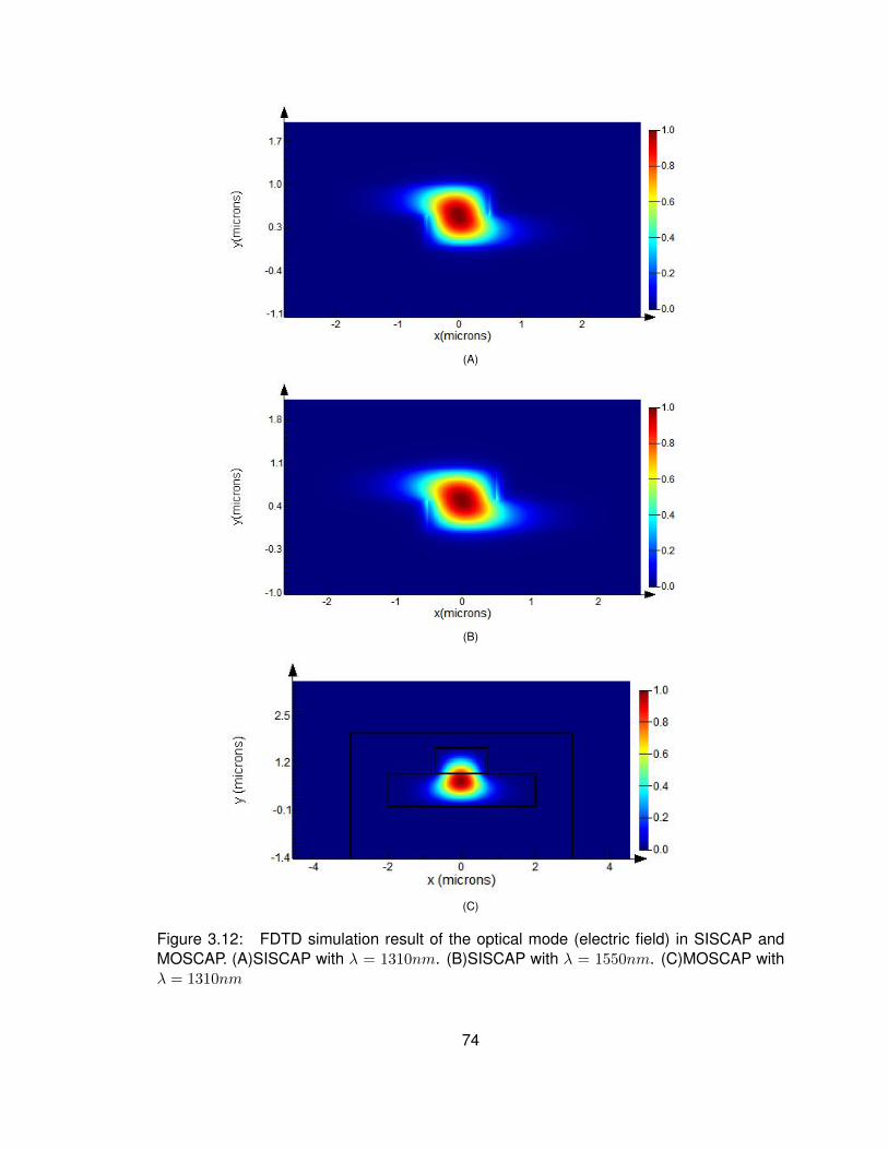
(A)
(B)
(C)
Figure 3.12: FDTD simulation result of the optical mode (electric field) in SISCAP andMOSCAP. (A)SISCAP with λ = 1310nm. (B)SISCAP with λ = 1550nm. (C)MOSCAP withλ = 1310nm
74

0 0.5 1 1.5 2 2.5 30
20
40
60
80
100
120
140
160
∆φ vs Voltage
Vsiscap(V)
∆φ(D
eg/
mm
)
Figure 3.13: FDTD simulation result of the phase shift in SISCAP.
the design efficiency has been dramatically improved. Circuit simulation can run very fast
and the result predicted by these models is very accurate compared to the measurement
data.
Although individual models have been developed for optical devices, the design of electri-
cal drivers and optical modulators are still two separate processes. The reason for this, as
explained in previous section, is because their working principles are quite different. A lot
of research efforts has been spent on creating a unified model strategy so that both circuits
and modulators can be simulated and optimized in the same software. Optoelectronic Sys-
tems Integration in Silicon (OpSIS) [86] developed by Luxtera is such a system supporting
electronic-photonic co-design through the electrical equivalent model of photonics devices.
The benefit of having SPICE like model for optical device is obvious. Designer can use the
flow they are familiar with to design optical chips - add optical and electrical devices to the
schematic, run simulation and optimize parameters, generate layout from the parameter-
ized cell (PCELL), execute design rule check (DRC) and layout versus schematic (LVS),
75

then tape out the design.
This section focuses on generating the SPICE compatible model of the optical modulator
at all hierarchy levels, from basic building blocks such as SISCAP to the whole modulator.
To mimic the real behavior, the model takes into account most of the non-ideal factors such
as loss, parasitics, temperature dependency and coupling - both capacitive and magnetic.
3.3.1. Model Hierarchy
The top level circuit model of the optical modulator is given in Figure 3.14. The modulator
IC model is mainly composed of three blocks: the lumped model of MZI, the on chip par-
asitic network consisting routing resistance and capacitance, the wire bond through which
the drive signal comes.
C(V)
MZI LUMPED MODEL
PARASITICNETWORK
ON OPTICAL
CHIP
R(V)
ATTENUATION(V) PHASE(V)
EinΦin
EoutΦout
From ElectricalDriver IC
+
-V
OPTICAL MODULATOR IC
Figure 3.14: Top level circuit model diagram of the SISCAP based MZI.
In the MZI model, there are two different types of signals: electrical and optical. The
electrical path is treated the same as in an traditional analog circuit since all the signals in
it are either voltage or current. The optical signal, on the other hand, can not be handled
by SPICE simulator directly because it is characterized by many factors other than voltage
or current. To circumvent this situation, two work-arounds are made. The first work-around
is representing the light simply by two properties: amplitude of its electric field, E and
relative phase, φ. The accumulation of the phase is not important because MZI work by
76

the phase difference. Any phase larger than 2π can be converted to 0 ∼ 2π without losing
any information. The other properties such as polarization and wavelength are taken care
of by other methods and not shown along this signal path. The second work-around is
treating all the electric field and phase of light as floating numbers going through a hyper-
wire. The hyper-wire only carry these two types of signals and can not be connected
directly to other circuit components like resistor or capacitor since the signal in it is not a
voltage or current.
The modulator model is created in a hierarchical manner, the same as its circuit coun-
terpart. Based on the model diagram, the model hierarchy is created and shown in
Figure 3.15.
1. OPTICAL IC
2. MZI 3. Bond wire4. On-ChipParasitics
5.SISCAP_RF 6. SISCAP_DC 7. Others
Figure 3.15: Model hierarchy created in this research.
Starting from the optical IC top, there are three components: MZI, bond wire and on-chip
parasitics. The first component process both electrical and optical signals whereas the
latter two only work with electrical signals. The MZI is further made up of three cells:
SISCAP RF for the high frequency modulation section in the MZI arm, SISCAP DC for the
DC bias point adjustment of MZI, and other auxiliary blocks such as passive waveguide,
Y-splitter, and Y-combiner etc.
The model of SISCAP RF is partially based on the previous work done at Lightwire, where
the capacitance and phase shift of SISCAP RF are described by two polynomials derived
77

from measurement data. This work enhances the accuracy of the previous model by
adding parasitic R, L, C information to the optical device. Besides the parasitic compo-
nents, the model also incorporates the voltage and temperature dependency. Geometry
dependent information is also added which means the final model is almost fully parame-
terized. Thus, the user can simply set the size, doping, voltage and etc to get the devices
performance simulated. This is an enhancement to an existing Lightwire model and makes
the model more complete.
3.3.2. Model of MZI
On the optical IC, MZI is the only device manipulating light. At this level, the MZI model
mainly focuses on the interconnection of each blocks. The loss and phase are processed
by the lower level model. The optical transfer function of MZI will be derived in this section.
Laser in Laser out
SOI
POLY
HYIN HRF HDC HYOUT
LRF LDC
HWG
Waveguide
Y-splitter RF section DC section Y-combiner
Left arm
Right arm
Figure 3.16: Optical transfer function in the MZI structure.
A close examination of the MZI structure as drawn in Figure 3.16 reveals that it consists of
a high frequency RF section, a low frequency DC section, a Y-splitter, a Y-combiner, and
several segments of passive wave guide. The signal flowing from the left to the right is the
laser represented by its electric field’s amplitude and phase. Each of these components
can be modeled as a black box, taking in the amplitude and phase signals, processing
them with some transfer function as shown in the figure, and then sending the results to
78

the output. The overall system transfer function can be written as
Eout = HY OUTHDCHRFHY INHWGEin (3.24)
where Ein is the amplitude of the input electric field.
Because there are only two branches in the MZI, a 2×2 matrix can be used in each block’s
transfer function. The phasor technique, found in the study of sinusoidal electromagnetic
waves, is adopted to simplify the derivation. With this technique, each element A in the
transfer function matrix can be simply expressed by
A = A0e−α+jθ (3.25)
where A0 is the amplitude, α is the loss coefficient representing the envelop of the ampli-
tude, and θ is the phase shift.
First, the light goes through is the Y-splitter. The function of a Y-splitter is to separate the
input laser power and send them to the two MZI arms. The transfer function of the Y-splitter
can be written as
HY IN =1√X + 1
·
√X 0
1 0
(3.26)
X is called split ratio which is the ratio of the output power between the two MZI arms. The
split ratio ranges from 0 to +∞. When X=1, the input laser power is equally distributed to
the two output ports corresponding to the ideal 3dB splitter. X values other than one can
be used to simulate the unbalanced case introduced by process fluctuation. The phase of
the light is not changed in this device. The loss of Y-splitter is a constant value which can
be lumped with other constant loss device later.
Then, the light enters the RF section where both of its amplitude and phase will be modu-
lated through the high speed electric field carrying information. The transfer function of the
79

RF section has the form of
HRF =
e(−αL+jφL) 0
0 e(−αR+jφR)
(3.27)
where αL and αR are the loss coefficient of the left and right RF section, respectively; φL
and φR are the phase shift of the left and right arm, respectively.
After RF section, light passes through the DC section which will also induce loss and phase
change, similar to the RF section. The difference is the loss and phase is in general fixed
after the initial configuration. The transfer function of DC section is
HDC =
e(−αDCL+jΦL) 0
0 e(−αDCR+jΦR)
(3.28)
where αDCL and αDCR are the loss introduced by the left and right DC tuning section,
respectively; ΦL and ΦR are the phase shift of the left and right arm, respectively.
Finally, the electric field and loss accumulated through all the previous devices are com-
bined in the last component, the Y-combiner. This device sums the two phasors from the
left and the right arms which, in optical terms, is called interference. The transfer function
of the Y-combiner is
HY OUT =1√X + 1
·
√X 1
1 −√X
(3.29)
The output of the Y-combiner is a 2 × 2 matrix whose (1,1) element is the phasor of the
final electric field Eout. Knowing Eout, the laser power is readily calculated by
Pout = |Eout|2 (3.30)
Now, let’s consider the background loss overlooked in the previous transfer functions. Loss-
es in our planar waveguide structure primarily come from three sources: absorption, scat-
tering, and radiation.
80

The absorption loss mainly originates from free carrier absorption and semiconductor band
edge absorption. The former one has been explained earlier in the free carrier effect. The
latter one occurs when photons’ energy is greater than the band gap energy of silicon
which, when translated into wavelength, is about 1.1µm. Since majority optical links only
work at either 1.31µm or 1.55µm, the loss caused by band edge absorption is not signifi-
cant, usually around 0.004dB/cm at 1.55µm [87].
Scattering in an optical waveguide may also come from two sources: interface scattering
and volume scattering. Interface scattering is caused by surface roughness. Volume s-
cattering is due to the bulk material imperfections which could be the crystalline defects,
voids, or contaminant atoms. For a mature process, loss from volume scattering is very
small.
The radiation in a well designed straight waveguide is negligible. However, when there is a
curvature in the waveguide such as in the Y-splitter, angle of incidence may change at the
waveguide wall, which may in turn result in some radiative loss.
All the losses except for the free carrier absorption loss are relative constant. In this work,
all these constant background loss in the Y-splitter, Y-combiner and waveguides, as men-
tion previously, are lumped into one transfer function of the waveguide and expressed as
HWG = e−αWGLWG (3.31)
where αWG represents the loss coefficient per unit length and LWG is the total waveguide
length. Losses in SOI waveguides are typically in the range of 0.1-0.5dB/cm [56].
3.3.3. Model of SISCAP
The SISCAP is the most complex component in the optical modulator. It handles both
electrical and optical signals. A simplified diagram of SISCAP showing all the electrical
components is given in Figure 3.17.
Electrically, the SISCAP is nothing but a series of lumped resistors and capacitors. These
81

P+
N+SOIGate Oxide
POLY
Va
OXIDE
RPFIX RPVAR
RNFIXRNVAR
C(V)
Figure 3.17: Electrical model of SISCAP created in this research.
R and C include the fixed resistors RPFIX and RNFIX in the electrode away from the
center region, the variable resistors RPV AR and RNV AR in the center overlap region, and
the voltage dependent gate capacitor C(V ). RPFIX and RNFIX model the silicon elec-
trodes’ bulk resistances which normally don’t change with the applied voltage, V a. RPV AR
and RNV AR, on the other hand, demonstrate some voltage dependency because they
are close to the center region where the carrier density changes significantly with V a and
hence influences the resistivity. C(V ), as discussed in Section 3.2.3, relies strongly on the
bias voltage.
Capacitance vs Voltage
Vsiscap(V)
Cap
acita
nce(
fF/u
m2 )
SimulatedMeasured
Figure 3.18: Measured SISCAP capacitance vs voltage and the comparison with curvefitting result.
All the fixed resistors can be modeled by the resistivity and geometry both of which are
easily obtained for a given process and design. Temperature coefficient is also added
82

to increase the model accuracy. However, deriving the analytical model of those voltage
dependent components is not that straight forward. They are influenced by multiple factors
such as doping level, switching frequency, and physical size etc, not to mention the voltage
and temperature. For these reasons, their models are created based on measurement data
under real conditions. The measurement result, usually collected at discrete conditions,
are fitted with a high order polynomial to interpolate the missing data points. Then, this
polynomial serves as a lower level function to be called by the final model with additional
constraints such as size, temperature, or doping level appended. The measured SISCAP
capacitance and the result from curve fitting are compared in Figure 3.18. Usually, higher
order polynomial has less fitting error. However, the interpolation result deviates quickly
from the expected values when the variable of the polynomial exceeds the measurement
range, as can be observed from the simulated curve in Figure 3.18.
When considering the optical structure, SISCAP needs to model two parameters: loss
and phase shift as mentioned in previous section. Since both parameters are determined
by the free carrier density change, a coupling variable must be chosen to connect the
electrical domain and optical domain, a similar situation as in the FDTD simulation. Not
like in the FDTD simulation where carrier density is available, the circuit simulator only
provides voltage and current. Without other options, voltage signal is selected as the
bridge between the two domains.
Due to the same complexity as in the modeling of variable resistors and capacitors, an
identical approach is applied to model the attenuation and phase shift in optical domain.
The measured attenuation and phase shift are plotted in Figure 3.19 along with their curve
fitting results.
To conclude this section, the model of DC section is briefly introduced. Since the purpose
of DC section is to introduce a fixed phase shift in order to bias the output power at the
quadrature point (See Figure 3.3), its model can be simplified by combining a background
loss with 0 phase shift on one arm and π phase shift on the other arm.
83

Attentuation vs Voltage
Vsiscap(V)
α V(d
B/m
m)
SimulatedMeasured
(A)
Phase Shift vs Voltage
Vsiscap(V)
θ(D
eg/m
m)
SimulatedMeasured
(B)
Figure 3.19: Measurement result and curve fitting comparison. (A)SISCAP attenuation vsvoltage. (B)SISCAP phase shift vs voltage.
84

3.3.4. Model of Bond Wire
P0
M0
P1
M1
Pn
Mn
Driver IC
Optical ICP0
M0
P1
M1
Pn
Mn
PCBDifferential Pair
(C)
Figure 3.20: Transmitter connection diagram.
In this work, the optical modulator is wire-bonded to the electrical driver who is further wire-
bonded to the PCB (printed circuit board) as shown in Figure 3.20. There are more than
10 bond wires running different data patterns in parallel with only 60µm distance between
them. Each bond wire has a length from 600µm to 800µm depending on location. The
accurate model of the bond wire parasitic is critical in this multi-gigahertz application since
these parasitics not only impact the signal going through the same wire but also influence
the adjacent circuitry through capacitive and inductive coupling.
In this work, the single bond wire is modeled as a self inductance (Lself ) in series with a self
resistance (Rself ) as given in Figure 3.21. The capacitive coupling is modeled through the
mutual capacitance Cmutual. The inductive coupling, or mutual inductance, is introduced
by the coupling coefficient k. Because of the small separation between wires, the coupling
coefficient is large even for wires 120µm away. Thus, coupling coefficients between bond
wires with distance of 60µm and 120µm are both captured.
85

Gold with diameter=0.8mil,Length from 600um~800um
Bond wire spacing=60um
Bonding PAD
Lself
k Cmutual
Rself
Lself Rself
(C)
Figure 3.21: Wire bond model.
3-D EM simulations are run to obtain the accurate value of each parameter. The simulation
results are plotted in Figure 3.22. In the model, the parasitic values are parameterized with
a table extracted from the plot.
3.3.5. Model of Routing Parasitic
The on-chip routing also adds significant parasitics to the electric signal path at high fre-
quencies. If the trace is long and the surroundings are simple, it can be simulated by 3-D
field solver as used in the bond wire modeling. This approach is not practical since in
general, the routings are short and crowded. The routing R, L, C, K parameters are finally
modeled by an S-parameter n-port model created from a 2.5-D field solver with acceptable
accuracy but much faster than the full 3-D simulator.
3.3.6. Simulation and Experiment Result
By incorporating all the models described in this chapter, the whole chip simulation is run
with the corresponding driver IC. The simulation results at different data rate are plotted
with the test chip’s measurement data in Figure 3.23. The comparison show our model is
in good agreement with the measurement.
86

100 200 300 400
0.08
0.1
0.12
0.14
0.16
0.18
Mutual Inductance vs Distance(len=800um)
Distance(um)
M(nH
)
500 1000 1500
0.2
0.4
0.6
0.8
1
1.2
1.4
1.6
1.8
2Self Inductance vs Length
Length(um)
L(nH
)
← len=800um L=0.68949nH
(A)
0 5 10 15 200.4
0.6
0.8
1
1.2
1.4
1.6
1.8
2
2.2
2.4Skin Depth vs Frequency
Fequency(GHz)
Skin
Dept
h(um
)
0 5 10 15 200.1
0.15
0.2
0.25
0.3
0.35
0.4
0.45
0.5
0.55
0.6Resistance vs Frequency
Fequency(GHz)
Resis
tance
( οhm)
(B)
500 600 700 8000.007
0.008
0.009
0.01
0.011
0.012
0.013
0.014Capacitance vs Length(D=60um)
Length(um)
Mutu
al Ca
pacit
ance
(pF)
500 600 700 8005.5
6
6.5
7
7.5
8
8.5
9
9.5x 10
-3Capacitance vs Length(D=120um)
Length(um)
Mutu
al Ca
pacit
ance
(pF)
(C)Figure 3.22: Simulation result of the bond wire model. (A)Self inductance and mutualinductance. (B) Skin depth and resistance for 800µm long bond wire. (C) Mutual capaci-tance for different bond wire distance ‘D’.
87

(A)
(B)
Figure 3.23: Simulated eye diagram (on the top) and measured optical eye diagram (onthe bottom) at different data rate. (A)10Gb/s. (B)28Gb/s.
88

3.4. Summary
This chapter focuses on creating an accurate model of the SISCAP MZM. After introducing
of the basic structure and operation principles of the modulator, fundamental parameters
of SISCAP are presented and derived. Then, the circuit model which enables the co-
design of optical modulator with electrical driver is proposed. Simulation results of major
parameters are given which matches the measured data pretty well. The model presented
in this chapter is extensively used in the optimization of the transmitter design for this work.
89

CHAPTER 4 : Optical Transmitter Performance Optimization
In an optical transmitter, the overall system performance can be evaluated by many param-
eters. These parameters, as mentioned in Chapter 2, include modulation speed, power
consumption, extinction ratio, optical modulation amplitude, chirp, and etc. In order to sup-
port the increasing demand in bandwidth originating from internet traffic, streaming video,
and exa-scale computing, modulators must be able to operate extremely fast while still
maintaining a very low power figure. This work mainly focuses on the modulator’s speed
and power optimization although other parameters are equally important. The chapter will
start with an overview of the transmitter architecture. Then, the approaches to achieve
maximum speed and reduce the power consumption will be discussed in detail. Finally,
the measurement result will be presented to conclude the chapter.
4.1. System Architecture
4x10G
Wirebond
CW LASER
DRIVER IC MZM IC
Figure 4.1: System architecture of the proposed optical transmitter.
The system architecture of the proposed optical transmitter is given in Figure 4.1. The
transmitter is composed of one electrical driver IC in 40nm CMOS and one optical MZM IC
in 0.13µm SOI CMOS. The driver IC receives 4 serial lanes of 10Gb/s electrical data and
recovers the data by on chip logics. The digital logic then merges the incoming data into
one 40Gb/s stream and sends them out through the MZI driver to the optical MZM which
90

is wire-bonded to the driver IC.
The reason of using two separate chips instead of one is not because of the technical diffi-
culty of the fabrication. Actually, since the SISCAP MZM is fundamentally compatible with
the prevailing CMOS process, the integration of MZM with the driver is readily achievable.
The main reason of designing two chip is for the speed concern as explained below.
Because of its high efficiency, the SISCAP MZM can be made fairly small, which means
its intrinsic bandwidth is very large. For example, with careful design, even using 0.13µm
process, the bandwidth can easily reach 20GHz which is capable of 40Gb/s modulation.
Currently, the actual speed bottleneck, as can be seen in the following sections, comes
from the electrical driver. Although the two-chip solution may potentially raise the cost, its
advantage is obvious: the design can be quickly moved from 10Gb/s to 40Gb/s or higher
data rate by just replacing the electrical driver by one that is fabricated in a faster process,
when it becomes available. So the design work can be saved by just refining the electrical
chip which may help reducing the system cost.
To make the system suitable for the major telecommunication and supercomputer appli-
cation, the design must follow or at least be close to some industrial specifications. After
some detailed comparisons, the IEEE802.3ba [88] 40Gb/s and 100Gb/s ethernet stan-
dard is chosen for this work.
The goal of the work is to demonstrate an optical modulator operating at 40Gb/s data
rate with modulation energy less than 300fJ/bit. After some investigations, it is found
that achieving both goal simultaneously is not a trivial task. Low power and high speed
are usually competing goals for a well designed system. Making one better will inevitably
degrade the other. This is the main reason why the input data is composed of four serial
data streams at 10Gb/s instead of other combinations.
There are four primary methods to increase the bandwidth:
91

1. Run more fibers in parallel.
2. Multiplex multiple wavelengths into one fiber such as in DWDM.
3. Increase the signal frequency which is the most straightforward way.
4. Encode more bits into one symbol which corresponding to the advanced modulation
scheme such as PAM-4 and QPSK.
This work only explores the last two approaches because the first two methods can be
easily implemented once the last two methods are successful. Thus, two optical modula-
tion schemes, OOK and PAM-16, as well as the corresponding drivers and modulators are
developed. Each scheme focuses on one of the two targets. Since the system involves
in both optical design and electrical design, optimizations on both of them will be studied.
The final goal now becomes
1. For the OOK transmitter, achieve 40Gb/s transmission data rate using single fiber
and single wavelength while keep the modulation energy, which is the energy re-
quired by the electrical driver to transmit 1 bit information, less than 5pJ/bit.
2. For the PAM-16 transmitter, reduce the modulation energy to less than 300fJ/bit for
short distance data bus applications.
In addition to these objective specifications, the transmitter also needs to meet some re-
quirements of the IEEE802.3ba standard. These requirements will be discussed with indi-
vidual block’s design.
4.2. Optical Modulator Performance Optimization
In this section, the approaches to improve the optical modulator’s performance will be pre-
sented. Both bandwidth enhancement and power reduction methods will be covered. The
trade-offs between different parameters are discussed. An advanced modulation scheme,
PAM-16, is introduced. Further investigation is also done to resolve the nonlinearity and
92

noise issues arising from this PAM-16 modulation. A novel method of doing on-chip polar-
ization detection is proposed in the end.
4.2.1. Bandwidth Enhancement
Silicon modulator’s intrinsic speed is limited by how fast the charge can be moved in and out
of the active region where optical mode is strong. As explained in Chapter 3, SISCAP MZM
is biased in the depletion or accumulation region where the charge density is controlled by
external electrical field. Hight speed will be achieved when the device relies on majority
carriers instead of minority carriers such as in the forward biased PN junction modulator.
Thus, the intrinsic bandwidth of the optical modulator is extremely high, only limited by
the RC time constant from the electrodes, and the electrical driver’s capability of pumping
current.
The electrical bandwidth of SISCAP can be written as
f−3dB =1
2πRC(4.1)
where R is the equivalent series resistance of the electrode between the two metal contacts
and C is the equivalent capacitance of SISCAP(see Figure 3.14). Both components are
voltage dependent as explained in Chapter 3.
The equivalent resistance R can be lowered by moving the contact closer to the center
overlap region or using higher doping level in the silicon electrodes. However, if the con-
tact is too close, the optical mode will partially extend to the heavily doped region under
the contact which introduces significant optical loss due to free carrier effect. The higher
doping has the same impact on the optical loss. Another approach to reduce R without
incurring too much attenuation is to use a controlled doping profile [89], where the doping
level is gradually reduced from the contact region to the center area, or from the top and
bottom to the gate oxide. The main idea is to make the doping level inversely proportional
to the optical intensity such that the absorption of light is minimized.
93
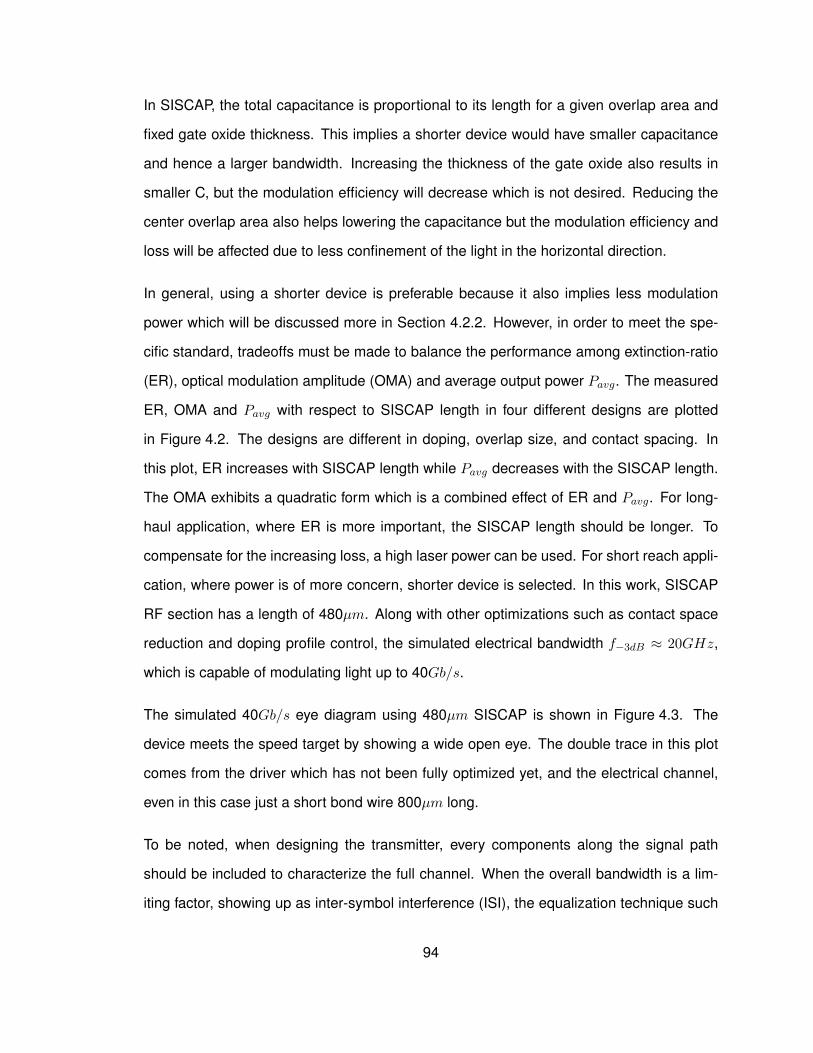
In SISCAP, the total capacitance is proportional to its length for a given overlap area and
fixed gate oxide thickness. This implies a shorter device would have smaller capacitance
and hence a larger bandwidth. Increasing the thickness of the gate oxide also results in
smaller C, but the modulation efficiency will decrease which is not desired. Reducing the
center overlap area also helps lowering the capacitance but the modulation efficiency and
loss will be affected due to less confinement of the light in the horizontal direction.
In general, using a shorter device is preferable because it also implies less modulation
power which will be discussed more in Section 4.2.2. However, in order to meet the spe-
cific standard, tradeoffs must be made to balance the performance among extinction-ratio
(ER), optical modulation amplitude (OMA) and average output power Pavg. The measured
ER, OMA and Pavg with respect to SISCAP length in four different designs are plotted
in Figure 4.2. The designs are different in doping, overlap size, and contact spacing. In
this plot, ER increases with SISCAP length while Pavg decreases with the SISCAP length.
The OMA exhibits a quadratic form which is a combined effect of ER and Pavg. For long-
haul application, where ER is more important, the SISCAP length should be longer. To
compensate for the increasing loss, a high laser power can be used. For short reach appli-
cation, where power is of more concern, shorter device is selected. In this work, SISCAP
RF section has a length of 480µm. Along with other optimizations such as contact space
reduction and doping profile control, the simulated electrical bandwidth f−3dB ≈ 20GHz,
which is capable of modulating light up to 40Gb/s.
The simulated 40Gb/s eye diagram using 480µm SISCAP is shown in Figure 4.3. The
device meets the speed target by showing a wide open eye. The double trace in this plot
comes from the driver which has not been fully optimized yet, and the electrical channel,
even in this case just a short bond wire 800µm long.
To be noted, when designing the transmitter, every components along the signal path
should be included to characterize the full channel. When the overall bandwidth is a lim-
iting factor, showing up as inter-symbol interference (ISI), the equalization technique such
94

480µm
ER vs SISCAP Length
SISCAP Length
Ext
inct
ion
Rat
io
Design1Design2Design3Design4
(A)
480µm
OMA vs SISCAP Length
SISCAP Length
OM
A
Design1Design2Design3Design4
(B)
480µm
Pavg vs SISCAP Length
SISCAP Length
Ave
rage
Pow
er
Design1Design2Design3Design4
(C)
Figure 4.2: Measured SISCAP MZI characters versus MZI length for different dopinglevels, center overlap lengths, and contact to center spacings. (A)ER change with MZI armlength. (B)OMA change with MZI arm length. (C)Average optical output power changewith MZI arm length.
95

Figure 4.3: Simulated optical eye diagram at 40Gb/s with 480µm SISCAP RF section.
as feed-forward equalization (FFE) can be implemented [90]. FFE pre-distorts the TX sig-
nal to compensate for the channel loss which dramatically improve the system bandwidth.
Thus, the receiver side can benefit from FFE with improved eye opening, power efficien-
cy, data rate and sensitivity. Implementing FFE is fairly easy in the SISCAP MZM. The
1-tap FFE can be realized by adding an extra FFE segment in the MZI arm as shown in
Figure 4.4. This segment, driven by a delayed and inverted version of the input signal,
shifts the output power up and down for a given delay time. The FFE tap coefficients,
determining how much distortion is added to the main signal, can be adjusted by using
different FFE segment length, or more conveniently changing the FFE driver’s supply volt-
age. This work doesn’t implement the aforementioned FFE because from our simulation
and test chip measurement, the system bandwidth is larger enough to sustain the 40Gb/s
data rate without any ISI problems.
Another potential problem in Figure 4.3 is the large rise and fall time which is about 17ps.
In this work, all devices are operated based on the lumped model simplification which
assumes it takes “zero” time for the electrical signal to be stable along the MZI arm. In
96

Wirebond
CW LASER
DRIVER IC MZM IC
1-tap FFEdriver
Main driver
Delay
Input
Figure 4.4: 1-tap FFE implementation in SISCAP MZM.
reality, light has a limited speed in silicon which is about 0.88×10⁸m/s. A quick calculation
shows the total time for light to go through a 400µm silicon waveguide is about 4.5ps. If the
electrical signal doesn’t match the speed of light, the wave front of light, already existing
in the MZI arm, will experience different phase shift and result in a longer rise and fall
time as given in Figure 4.5. The traveling wave model has been studied by many groups.
0 2 4 6 8 100
0.2
0.4
0.6
0.8
1
1.2
1.4
1.6
1.8
2Without traveling wave matching
∆φ(r
ad)
Time(ps)0 2 4 6 8 10
0
0.2
0.4
0.6
0.8
1
1.2
1.4
1.6
1.8
2With traveling wave matching
∆φ(r
ad)
Time(ps)(A) (B)
Figure 4.5: ∆φ change in the MZM. (A)Without traveling wave matching. (B)With travelingwave matching.
A comprehensive model using chained S-parameter and progressively propagating EO
97

functions was created [91]. The 4.5ps rise time in Figure 4.5, compared to the total data
period at 40Gb/s (25ps per bit), is large and can be a big issue at high data rate. Achieving
velocity matching in SISCAP MZM is not as simple as in the MOSCAP or P-i-N junction
based modulators where traveling wave electrodes are implemented [60, 62]. In SISCAP
MZM, one possible solution to mitigate the velocity mismatch is to split the long SISCAP
segment into multiple smaller pieces and drive them separately. Then, a small delay could
be introduced to each driver to mimic the wave propagation behavior in a traveling wave
electrode. However, generating a delay on the order of 1ps is extremely challenging with
CMOS circuit. Any non-ideal factors, such as transistor mismatch, supply noise, process
and temperature variation could incur a delay much larger than 1ps. For this reason, no
velocity matching circuit has been designed in this work.
(A) (B)
(C) (D)
Figure 4.6: Measured OOK modulation eye diagram from the test chip. (A)32Gb/s PRBS7electrical input. (B)32Gb/s PRBS7 optical output. (C)40Gb/s PRBS31 electrical input.(D)40Gb/s PRBS31 optical output.
98

To verify the architecture’s capability, an optical test chip along with the corresponding
electrical driver IC are fabricated. In the optical IC, various test structures are designed
to characterize the optical components such as wave guide, MZI, and on chip parasitic
R, L, and C. In the electrical IC, building blocks to control the laser source power, DC
bias point of MZI, and temperature are also designed. These blocks can be reused in the
final transmitter. Sensor circuits to measure light intensity and voltage are also developed.
Digital synthesized logic that puts all these sense and control circuitries into a feedback
loop is also on the same chip.
The measurement result of this test chip is plotted in Figure 4.6. The electrical inputs
(Figure 4.6(A), (C)) are generated directly by a high speed pattern generator. The results
show a wide open eye of the output laser signal running at 32Gb/s with PRBS7 data
pattern. The power dissipation numbers match simulations - i.e. about 400mW (Total
power including supporting circuitry), at room temperature. The data rate can even go up
to 40Gb/s by stressing power supply voltage as shown in Figure 4.6(D). In the mean time,
the optical structures with different parameters are tested to acquire the information for the
accurate modeling.
4.2.2. Power Reduction
The analysis of the power consumption is first conducted in this section to identify all the
contributors. Then, methods to reduce the power are discussed. As a result, an advanced
modulation scheme, PAM-16, is proposed.
Power Consumption in SISCAP MZM
Power consumption is a critical specification in optical modulator design since it may influ-
ence chip temperature, power grid, link density, and long term reliability. Analysis shows
the majority power other than laser source in the optical transmitter is consumed by switch-
ing the MZM on and off. A simplified circuit diagram showing both the SISCAP MZM and
the driver is shown in Figure 4.7. In this diagram, the MZM loading is represented by
99

C(V)
MZMR(V)
VDD
GND
Figure 4.7: Simplified MZI driver diagram for power consumption analysis.
lumped R and C. The driver is a CMOS inverter consisting of a PMOS and an NMOS.
Under such configuration, the power consumption can be roughly categorized into two
groups: dynamic Power and static Power. The total power is
PTOTAL = Pdynamic + Pstatic (4.2)
Dynamic power mainly arises from two sources: switching power due to charging and dis-
charging of the load capacitance, short circuit power due to “crowbar” current flowing from
VDD to GND while switching. The switching power is proportional to the load capacitance,
operating frequency and square of the supply voltage. The crowbar current should be zero
if the input signal switches infinitely fast. However, due to parasitic RC, the input signal
exhibits a finite slope. During this transition when VTHN < VIN < (VDD − VTHP ), where
VIN is the input voltage and VTHN , VTHP are the threshold voltage for NMOS and PMOS
respectively, both transistors will be turned on and conducting current simultaneously. The
short circuit power depends on the rise/fall time (trise,fall) of the input, the supply voltage
(VDD), and the switching frequency (f ). The factors impacting dynamic power can be
summarized as
Pdynamic =
Pswitching ∝ CV 2
DDf
+
Pcrowbar ∝ trise,fallVDDf
(4.3)
100

Static power is due to sub threshold leakage currents, source/drain junction reverse-bias
current, and gate leakage current caused by tunneling effect. The parameters influencing
static power can be summarized as [92]
Pleakage ∝
WL
e−VTHkT/q
1− e−VDSkT/q
(4.4)
Advanced Modulation Scheme: PAM-16
For a given CMOS process, the threshold voltages of the transistors are fixed. The supply
voltage, required by the SISCAP MZM, also has little room to reduce. Otherwise, the
modulation efficiency will drop. The transistor size, working temperature and rise/fall time
depend on the specification and can not be easily changed. Thus, the only knob left to
reduce the power consumption is the switching frequency (symbol rate) - f , as can be
seen from Equation (4.3) and (4.4).
Reduction in f is possible through advanced modulation schemes such as PAM-N and
QPSK, as introduced in Section 2.2.2. Advanced modulation has been drawn considerable
research attention in the past few years because it is a promising approach in reducing the
system cost and complexity beside its high spectral efficiency [93]. Among all possible
schemes, the PAM-N modulation is of particular interest for the SISCAP MZM because it
can be easily implemented using a so-called segmented MZI configuration [94].
In order to generate multiple output intensity levels, prior optical modulators such as QAM-
64 [38] typically employ a digital-to-analog converter (DAC) in the electrical driver. The
DAC generates different analog signal levels to properly drive the modulator according
to the digital input. For example, to generate 16 output levels, a 4-bit DAC should be
employed. In SISCAP MZM, since the output intensity is proportional to the SISCAP
length, the optical DAC feature can be realized directly by cascading multiple SISCAP
segments [94] with very little change in the corresponding driver - same inverter structure
with same supply voltage can be used. For example, in a PAM-16 modulator, there could
101

be four SISCAP segments with their lengths in a binary code weighted manner where each
segment is driven by its own inverter driver. This segmented structure can be applied to
both PAM and PSK modulation schemes with any number of levels, subject only to other
system constraints such as SNR, receiver complexity, and etc. The eye diagrams of PAM-2
(OOK), PAM-4 and PAM-16 are plotted in Figure 4.8.
(A) (B) (C)
Figure 4.8: Different PAM schemes. (A)PAM-2(OOK). (B)PAM-4. (C)PAM-16.
The power saving in PAM-N, while comparing with OOK (or PAM-2), comes twofold.
First, since the spectral efficiency (SE) in PAM-N is log2N b/s/Hz, the symbol rate fPAM−N
becomes log2N times smaller than the original symbol rate f . For example, if N=16, the
SE is 4b/s/Hz and the symbol rate is 10GBaud/s for 40Gb/s data rate. Theoretically, from
Equation (4.3), the switching power in PAM-16 is only 1/4 of the OOK with the same data
rate.
Second, in PAM-N, a long MZI arm is broken into multiple segments while the total length
is unchanged to maintain the same OMA. Shorter MZI segment has smaller capacitance
which only requires small sized inverter as the driver. Thus, the leakage power can be
reduced from Equation (4.4). Further more, due to the input data’s random nature, not all
the segments need to be switched simultaneously. As a result, the effective capacitance in
Equation (4.3) becomes smaller which helps reducing the switching power further.
Aside from the big power savings, implementing PAM-N also has other benefits. Since the
symbol rate in PAM-N is reduced by log2N times, the circuit design now becomes much
easier. This implies, with the same symbol rate, the data rate could be log2N times higher.
With the improved the SE in PAM-N, the channel spacing in a DWDM system can be further
102

reduced which also helps increasing the capacity.
The disadvantage of PAM-N mainly lies in the complexity for the receiver design. To detect
multiple light levels, a linear transimpedance amplifier (TIA) must be employed which needs
more design efforts than the limiting amplifier in an OOK link. Besides, an analog-to-digital
converter (ADC) must be used to sample the input signal and convert them into digital data.
Designing such an ADC working at more than 10Gsample/s sample rate is never a trivial
task. The signal processing and clock and data recovery (CDR) also become significantly
more complex. Whereas in the OOK system, the sampling job is simply done by a D flip-
flop. All the above circuit changes may finally consume more power than the power savings
from the transmitter. In addition, multiple levels result in a worse SNR performance and
lead to increased BER. On the transmitter side, the free-carrier effect may incur phase
dependent loss and cause unbalance to the two MZI arms if the segment structure and its
driving sequence is not properly designed. Thus, design tradeoffs must be made in system
level as well as in block level.
Binary code weighted PAM-16
Thermometer code weighted PAM-16
MZI RF
MZI DC
WAVEGUIDE
15lOOK
(PAM-2, NRZ)
l 2l 4l 8l
l l l l l l
15 segments
Figure 4.9: Implementation methods of PAM-16 with segmented SISCAP MZM: PAM-2or OOK (top), binary code weighted PAM-16 (middle) and thermometer code weightedPAM-16 (bottom).
PAM-N modulation scheme, utilizing the aforementioned optical DAC feature, could be im-
plemented in several different ways (Figure 4.9). The simplest form is to make the segment
length binary code weighted. For example, in PAM-16 as shown in Figure 4.9, there are
4 segments in each MZI arm with lengths of l, 2l, 4l, and 8l. To obtain the same OMA in
PAM-16 as in OOK, their MZI total length should be equal, which is 15l in the plotted case.
103

The MZI can also be composed of 15 segments with identical length l which is called ther-
mometer code weighted PAM-16. The digital data is mapped to the control signals of MZI
using an encoding table as given in Table 4.1.
Table 4.1: Encoding table for different PAM-16 implementations.Control of binary code Control of thermometer code
Input Data weighted PAM-16 weighted PAM-16MSB-LSB Left-Right
0 0000 0000000000000001 0001 0000000000000012 0010 0000000000000113 0011 0000000000001114 0100 0000000000011115 0101 0000000000111116 0110 0000000001111117 0111 0000000011111118 1000 0000000111111119 1001 000000111111111
10 1010 00000111111111111 1011 00001111111111112 1100 00011111111111113 1101 00111111111111114 1110 01111111111111115 1111 111111111111111
By going from binary code weighted segments to thermometer code weighted segments,
further power saving can be achieved since the effective capacitance becomes smaller.
Simulation results show an 82.5% and 88.8% power savings for binary and thermometer
code weighted PAM-16 from OOK modulation. Theoretically, the power can be further
reduced by increasing the number of levels at the expense of increased receiver complexity
and small optical SNR due to the reduction of the eye height.
Enhanced Binary Code Weighted PAM-16
In previously described PAM-16 modulation schemes, the amplitudes between adjacent
optical levels are not equal due to the raised cosine transfer function of MZM as shown
in Figure 4.10(A). With a linear change in the phase shift ∆φ, the amplitude difference
between adjacent levels close to the middle is larger than that close to the top and bottom.
104

OPTICAL POWER
0 π∆Φ0 π 2π
∆Φ2π
OPTICAL POWER
(A) (B)
Figure 4.10: (A)Binary/thermometer code weighted PAM-N (N=8 in this plot).(B)Enhanced binary code weighted PAM-N (N=8 in this plot).
This nonlinearity is a serious problem for the receiver because the analog front-end and
the CDR algorithm are all based on linear input. To resolve this nonlinearity issue, an
enhanced binary code weighted MZI structure is proposed which features a transfer curve
as given in Figure 4.8(B).
The implementation of the enhanced binary code weighted PAM-16 scheme is shown in
Figure 4.11. An extra segment is introduced to the original 4-segment binary code weight-
Skew adjustment
Figure 4.11: MZM structure implementing the enhanced binary code weighted PAM-16scheme.
ed MZI and the segments’ lengths are not strictly binary weighted. The added segment
introduces 1 bit redundancy to the DAC hence creating 32 levels. Numerical analysis is
used to determine the best segment length where there are 16 levels out of the 32 level-
s that are the closest to the ideally equally spaced 16 positions. A digital encoder is also
required to map the 4 bit input signals to the desired 5 output signals driving each segmen-
105

t. In addition to generating 16 output levels, by loading different encoder tables, PAM-2,
PAM-4 and PAM-8 can also be realized using the same MZM design. To implement such
programmable PAM transmitter, the encoder simply skips the unused levels in these three
new configurations.
To better understand the working mechanism of this modulation scheme, an example
showing enhanced binary code weighted PAM-4 is given in Figure 4.12. The 4 level-
A1
A2
A3
A4
C1
C2
C3
C4
B1
B3
B7
B8
B2
B4
B5
B6
DA34
DA23
DA12
DC34
DC23
DC12
(A) (B) (C)
Figure 4.12: PAM-N (N=4 in this plot) level position optimization. (A)Before optimization:the 4 levels are unequally spaced. (B)Using 3 SISCAP segments with random lengths togenerate 8 levels. (C)After optimization: 4 levels with equal space are pick from (B) to getthe final PAM-4.
s, A1 ∼ A4, of a binary code weighted MZM are plotted in Figure 4.12(A). Due to the
nonlinear transfer function from Equation (3.4), the level difference DA23 is larger than
DA12 and DA34. By introducing a third segment, 8 levels, B1 ∼ B8, are created as
shown in Figure 4.12(B). The total MZI length is still unchanged to have the same O-
MA (A4 − A1 = B8 − B1). Now, because the 3 segments can have arbitrary length as
long as their total length is the same, the middle 6 levels, B2 ∼ B7, can be placed in any
positions between B1 and B8. Among all possible length combinations, there must be one
case where 2 levels, B4 and B6 in Figure 4.12(B), can be found at the same positions as
C2 and C3 which split the total OMA into 3 equal parts (DC12 = DC23 = DC34).
106

The previous enhancement technique is based on the assumption that the noise power is
the same for all levels. Thus, it focuses on how to get equally spaced output levels which
will give the best BER performance. However, in some occasions, it is not the optimum
from the system perspective. For example, when the optical link is shot noise limited,
higher output levels demonstrate larger variation in intensity around its average value as
depicted in Figure 4.13(A). As shown in Section 2.3.1, the photon shot noise is proportional
Inte
nsi
ty
Probability
Inte
nsi
ty
Probability
(A) (B)
Figure 4.13: Output intensity distribution in PAM-N. (A)With equally spaced output levels.(B)With optimum output level spacing.
to the average light power. Thus, the SNR increases with the square root of the average
power. The sensitivity of the receiver is then limited by the upper two levels where in order
to avoid bit errors, the judgement threshold must be larger than the crossing point of these
two levels. In order to minimize the error probability between levels, system should be
designed with unequal output levels as shown in Figure 4.13(B).
It can be shown that, when the electrical fields of each level are equally spaced, or the
intensity has a quadratic spacing, the system’s error performance is optimum [42]. When
considering other noise types such as thermal noise, the optimum level could be differen-
t [95].
Simulation result
In this work, the MZM employing the enhanced binary code weighted PAM-16 scheme is
chosen as the final design. The simulated eye diagram, using the model created in Chapter
107

3, is plotted in Figure 4.14. Two different data rates are simulated: 40Gb/s and 112Gb/s.
(A)
(B)
Figure 4.14: Simulated PAM-16 optical eye diagram with PRBS31 pattern. (A)Data rateis 40Gb/s with symbol rate = 10GBaud/s. (B)Data rate is 112Gb/s with symbol rate =28GBaud/s.
To get the best eye, the inverter driver must be properly sized. The eye diagrams in both
cases show 16 distinct levels with equal space. This proves the enhanced binary code
weighted PAM-16 scheme is working.
108

4.2.3. Polarization
The sub-micron SOI waveguide employed in this work is polarization dependent. As shown
in the perturbation theory [84], the modulation efficiency is only maximum when the opti-
cal signal in SISCAP is TE mode. Thus, to guarantee the best performance, detecting
and changing the polarization status is important in the optical transmitter. In the optical
image-rejection receiver of a PolPSK system, the incoming signal needs to be 45 linearly
polarized with respect to the receiver’s polarization direction [42]. Thus, knowing the polar-
ization status is critical to properly demultiplex the signal. Existing solutions, using external
components to detect the polarization changes, are usually bulky and expensive. Design-
ing polarization detector which can be integrated with silicon is always an active topic in
industries and universities.
To illustrate the concept of polarization detection, a fully CMOS compatible polarization
imager has been designed and tested, which will be described in the next section.
4.2.4. Integrated Polarization Detection Imager
Polarization is one of the important characteristics of light that can not be detected directly
by traditional photo detectors. This work explores the possibility of using the on-chip metal
wire grid to detect the polarization status of light. We propose an image sensor integrated
with focal plane 2 × 2 wire-grid polarizer filter mosaic targeted at visible spectrum, which
enables the reconstruction of the polarization response characteristic [96]. FDTD method
is employed to optimize the extinction ratio in visible spectrum of the multi-layer focal plane
wire-grid polarizer. Experimental results show that an extinction ratio around 10 is achieved
with a standard error of around 0.25% between the experimental results and the fitting
sinusoidal polarization response curve. A phase error of less than 2% to the measurement
phase resolution is achieved. These results are the best reported for a monolithic wire-
grid polarization image sensor design for visible spectrum. The same concept can be
easily extend to the communication wavelength range. The only requirement is to have an
109

integrated photo detector sensitive in these wavelength because silicon can not detect light
with wavelength longer than 1.1µm. As the recent advancement in fabrication technology,
such integrated photo detector has been successfully demonstrated [97].
Traditional photo detectors[98, 99] only detect and encode two characteristics of visible
light, intensity and wavelength, interpreted as perceptual qualities of brightness and color.
Another important characteristic of light, namely, polarization, has not been effectively ex-
ploited. Inspired by the fact that the eyes of some animal species (e.g., honeybees, desert
ants, shrimps) can sense the polarization of light for navigation and improved vision, vari-
ous research projects have been reported, exploring the potential of polarization in remote
sensing, fingerprint detection, and sensing object illuminated by low intensity source light.
Early approaches towards polarization imaging employed a precise, but bulky optical set
up, including standard image sensing devices and separate polarization filters, such as
rotating polarization elements, or orthogonal polarization filters and beam splitter. Taking
advantage of the development of nano-fabrication technologies, integration of image pro-
cessing/light filtering at the focal plane, within each pixel is available [100, 101, 102, 103].
However, the fabrication methods require post processing of the imagers which makes it
not only expensive but also hard to align the filter on top of the pixels. This limits this ap-
proach to low-resolution imagers. Also the filters on top of a relatively thick oxide causes a
poor extinction ratio for non-normal incident light beams.
In this work, a three-dimensional wire-grid polarizer model is built based on CMOS pro-
cessing technology. The optimization of the extinction ratio performance of the wire-grid
polarizer in the visible spectrum is explored. A 32 × 32 active pixel sensor (APS) array
integrated focal plane 2 × 2 metallic wire-grid polarizer filter mosaic with independent ori-
entations on the same substrate has been fabricated in 65nm standard CMOS processing
line. Current readout mode is employed, taking the advantage of an easy implementation
of algebraic processing for focal plane level polarization reconstruction. Although the pro-
posed design is targeted at the visible spectrum, our simulations show the wire-grid also
110

has a good polarization response at the communication wavelengths.
The section is organized as follows. First, a numerical analysis is performed on a multi
metallic layer wire-grid design model based on standard CMOS technology. Architecture of
a CMOS image sensor array integrated focal plane wire-grid polarizer filter mosaic is then
proposed followed by the experimental results. Finally, the proposed work is compared
with previous results reported in the literature, which concludes this section.
Design of Focal Plane Wire-Grid Polarizer
Multi-layer metallic wire-grid gratings can be integrated on top of photo detectors using
standard CMOS processing. A simple diagram illustrating the basic principle of metal wire
grid is shown in Figure 4.15. When unpolarized light is passing through the wire grid, the
Figure 4.15: Metal wire grid for polarization filter.
electrical field will interact with the metal differently depending on its polarization status.
When the electric field is in parallel with the metal wire, most of the light will be reflected,
resulting in a minimum output power. When the electric field is perpendicular to the wire,
maximum transmittance is achieved.
In order to evaluate the efficiency of a polarizer, Polarization Extinction Ratio (PER) is
introduced into the theoretical analysis of polarization. PER is defined as the ratio of the
111

maximum and minimum transmitted power of the incident light. Typically, PER is expressed
as a fraction, in dB, as follows,
PER = 10log
(PmaxPmin
)= 10log
(T⊥T‖
)(4.5)
where T⊥ and T‖ represent the transmission efficiency of the wanted and unwanted inci-
dent lights passing through the wire-grid.
Finite-Difference Time-Domain (FDTD) method is employed to provide a computational
electrodynamics solution for the propagation of an orthogonal linear polarized incident light
based on the Maxwell’s Equations. The wire-grid dimension size is optimized with respect
to maximizing the extinction ratio. Assume the wire-grid is infinitely extended along the y-
axis direction, as shown in Figure 4.16, the dimension of the wire-grid can be defined by 1)
wire-grid period (Λ); 2) the duty cycle (W/Λ×100%) as the percentage of one period that is
occupied by metal wires; 3) the vertical thickness of the wire-grid (h); and 4) the material of
the wire which it is made of. For a selected CMOS processing, the thickness and material of
the wire-grid are fixed. In the following, the 65nm standard CMOS processing technology
is used to demonstrate a performance analysis on CMOS implemented wire-gird polarizer.
Figure 4.16: FDTD simulation model (right) and electrical field (left) of metal wire gridpolarization filter.
Figure 4.17 shows the simulated extinction ratio for a single layer wire-grid made of the
112

first metal layer (denoted as M1), while the wire-grid period Λ is increasing from 100nm
to 180nm with a fixed wire-grid duty cycle of 50%, or the duty cycle of the wire-grid is
increasing from 40% to 80% with a fixed Λ = 200nm, respectively [96]. The extinction ratio
is evaluated for different wavelengths varying from 450nm to 650nm. The results clearly
show smaller periodic size and higher duty cycle provides a higher extinction ratio. The
extinction ratio increases approximately 5dB for every 40nm decrement of the period Λ
or every 10% increment of the duty cycle the period of the wire-grid shrinks by 100nm for
650nm incident. However, the transmission efficiency of both the wanted and unwanted
light is dramatically reduced for increasing duty cycles. Considering the sensitivity level of
a standard CMOS image sensor, a duty cycle around 50% is recommended.
100 110 120 130 140 150 160 170 1800
5
10
15
20
25
30
Pol
ariz
atio
n E
xtin
ctio
n R
atio
/ dB
Wire−grid period Λ / nm
IBM65nm wire−grid Λ=2W 10000
λ=0.45umλ=0.55umλ=0.65um
0.4 0.45 0.5 0.55 0.6 0.650
5
10
15
20
25
30
Pol
ariz
atio
n E
xtin
ctio
n R
atio
/ dB
Wire−grid duty cylce W/ Λ
IBM65nm wire−grid Λ=200nm M1 used
λ=0.45umλ=0.55umλ=0.65um
(A) (B)
Figure 4.17: Simulation results of the extinction ratio for a single layer wire-grid made ofthe first metal layer (M1), while (A) wire-grid period Λ is increasing from 100nm to 180nmwith a fixed wire-grid duty cycle of 50%; (B) the duty cycle of the wire-grid is increasingfrom 40% to 80% with a fixed Λ = 200nm. The extinction ratio is evaluated for differentincident wavelength varying from 450nm to 650nm.
There are different combinations of the metal layers for the implementation of the wire-grid.
Different selection changes the interference, or to say the propagation of the incident wave,
which effects the amount of absorbed energy in the substrate. Figure 4.18 compares the
extinction ratio of different patterns [96]. The results are quite interesting. There is no
preferred layer for the vertical wire-grid location. It varies due to the interference between
the wire-grid and the substrate, which depends on the wavelength of the incident wave.
113

Figure 4.18: A comparison of the extinction ratio performance while different metal layeris selected for a single layer wire-grid implementation.
Implementing multiple layers of wire-grids of the same dimension will further reduce the
total absorption of both the wanted and unwanted incidents. To study the effect of the
number of metal layers to build the wire-grid polarizer we increased the number from 1 to
5 layers. According to the numerical results, a dual-layer wire-grid realizes a 25dB higher
extinction ratio than a single-layer structure. A triple-layer structure can further increases
the extinction ratio performance by another 20dB. However, if more than two metal layers
are included in the gratings, the maximum transmission efficiency will be less than 1%.
Considering the sensitivity of a CMOS photodiode, the light intensity level will be too low
to be distinguished from the noise.
Simulations are also run with the same wire-grid setup at communication wavelength
range. The extinction ratio and transmission and reflection efficiencies with different wave-
lengths are plotted in Figure 4.19. The result are collected for distance between wire-grid
and the substrate from 50nm to 200nm. When the distance is shorter, the extinction ratio
is higher. This result is a little different comparing with Figure 4.18. The main reason is
because for longer wavelength, the interference between wire-grid and substrate is much
114

1.2 1.3 1.4 1.5 1.6-10
0
10
20
30
40
Ext
inct
ion
Rat
io /
dB
Λ=140nm H=125nm w=70nm Cu
Wavelength / um
D=50nmD=100nmD=150nmD=200nm
1.2 1.3 1.4 1.5 1.60.4
0.5
0.6
0.7
0.8
0.9
1
Tra
nsm
ittan
ce T
⊥
Λ=140nm H=125nm w=70nm Cu
Wavelength / um
D=50nmD=100nmD=150nmD=200nm
1.2 1.3 1.4 1.5 1.60
0.2
0.4
0.6
0.8
Ref
lect
ance
R⊥
Λ=140nm H=125nm w=70nm Cu
Wavelength / um
D=50nmD=100nmD=150nmD=200nm
Figure 4.19: Simulation result of metal wire grid polarizer at communication wave length:ER (top), transmission efficiency T⊥ (middle) and reflection efficiency R⊥ (bottom).
115

less. This simulation proves the proposed wire-grid to be a possible approach for commu-
nication applications.
Architecture of CMOS Image Sensor with Focal-Plane Polarizer
A 32 × 32 current mode active pixel sensor (APS) array integrated focal-plane wire-grid
polarizer with various design patterns are fabricated in 65nm processing. The overall pixel
structure is illustrated in Figure 4.20(A) [96]. The photo detection process starts with a
reset phase in which the photodiode voltage is pulled up to the preset voltage VRESET .
During the exposure phase, the photodiode voltage will be discharged proportionally to the
incident light intensity and integration time. An analog current is readout after exposure. A
chain of shift registers are integrated in the vertical/horizontal control units for the selection
of reset/readout pixel. Since current mode APS enables easy implementation of focal plane
algebraic processing, such as addition, subtraction, current mode is employed for the pixel
value readout.
The sensor array is divided into 2 × 2 blocks. In each block, the photodiode area of three
pixels are covered by metallic wire-grid polarizers. Limited by the design rule, the minimum
wire width is 90nm. A minimum slit gap distance between two gratings of 90nm is required.
As shown in Figure 4.21, different layout patterns of the gratings are implemented for a
experimental comparison, including
1. single layer metallic grating with a metal duty cycle of 50%. Different selections of the
gratings metal layer are implemented;
2. multi layer metallic gratings with a same dimension of the grating width (w) and period
(Λ) are implemented;
3. different grating layout orientations are implemented, such as 0, 90 and 45.
The 45 wire-grid is implemented using staggered square pattern with a minimum width of
90nm to meet the design rule of the processing as shown in Figure 4.20(C). The minimum
116

(A)
(B) (C)
Figure 4.20: (A) Circuit diagram of the overall system. The 32 × 32 active pixel sensor(APS) array is divided into 2 × 2 blocks. Within each block, three wire-grid polarizer filtersare implemented on top of the photodiode region. The architecture of the pixel and currentconveyor is illustrated on the right. (B)Microphotography of the the polarization imagesensor. (C)Layout of the 45 wire grid with an effective period of about 250nm.
117

(A) (B) (C)
Figure 4.21: (A)Metal stack of the 65nm CMOS process. (B)Wire grid cross section.(C)Pixel mosaic structure.
width of each piece of the lines is 90nm. The minimum effective distance between two 45
wires is about 125nm, resulting in a minimum period of about 250nm. A microphotography
of the sensor array is illustrated in Figure 4.20(B).
Experimental Results
Figure 4.22: Test setup of the polarization image sensor.
In the test setup as shown in Figure 4.22, an off-chip 12-bit ADC is connected to the data
bus of the imager to digitize the pixel’s readout value. We first examine the response to
differently polarized incident light. A LED array is used to as light source. A diffuser is
placed in front of the LED light. A polarizer is used to convert the incident light to a linearly
118

polarized wave. The digitized output is collected for further analysis.
Polarization describes electronic field (E vector) changes of a uniform plane wave. Gener-
ally, the locus of E vector is an ellipse, and the observed intensity of partially polarized light
I can be expressed as a function of energy intensity IU , the degree of linear polarization p,
and the orientation angle ψ of the ellipse as follows [104]:
Iχ = IU [1 + pcos(2ψ − 2χ)] = IU + IAcos(2ψ − 2χ) (4.6)
where χ is the ellipticity angle of the E vector ellipse. In each block, three polarizers
with different wire-grid orientations have been implemented. We tested the polarizer by
changing the ellipticity angle χ of the linear polarized incident from 0 to 180 in steps of
10.
Figure 4.23(A) shows the measured transmission efficiency for pixels covered by wires
with a different wire-grid layout orientations in a same block [96]. The digitized pixel value
is normalized by the intensity captured by standard pixel without wire-grid on top. The plot-
ted value is a mean of the measured value from various pixels covered by wire-grid with a
same layout orientation. An average extinction ratio of 9.26 (9.67dB) and 7.79 (8.92dB) is
achieved for a 0 and 90 wire-grid, respectively. Due to the saw-toothed layout implemen-
tation, the effective period of the 45 is larger than 250nm, resulting in a lower extinction
ratio and a higher transmission effective. The standard error between the experimental
results and the fitting sinusoidal curve is 0.26%, 0.24% and 0.19% for a 0, 90 and 45
wire-grid, respectively. The phase difference between the fitting curves of 0 and 90, 0
and 45 is 87.13 and 45.62 comparing to an expected phase difference of 90 and 45,
respectively. The phase error of each measured angle between the testing results and the
fitting characteristic is illustrated in Figure 4.23(B).
Compare to the testing phase resolution is 10, the average phase error is 1.94%, 1.36%
and 2.43% for a 0, 90 and 45 wire-grid, respectively. The experimental results are the
best reported for a monolithic polarization image sensor designed for visible wavelength
119

range.
(A)
(B)
Figure 4.23: Measurement result. (A)Transmission efficiency. (B)Phase error of pixelscovered by wire-grid with a different layout orientations of 0, 45 and 90. The degreevalue on the x-axis is the rotation angle of the polarizer on the path of the incident.
However, it should be noted that the extinction ratio is not as good as the theoretical results
due to the crosstalk issue between pixels covered by wire-grid with different orientations
within a same sub-block. A higher extinction ratio is always measured for boundary pix-
els, since the crosstalk effect is reduced by a half. A maximum extinction ratio of 14.37
(11.57dB) and 10.14 (10.06dB) is measured for boundary pixels with 0 and 90, respec-
tively.
Discussion
In this work, a 2 × 2 polarizer filter mosaic with independent wire-grid layout orientations
120

Figure 4.24: Sample image of the polarization image sensor.
for different pixel using standard CMOS technology is presented. A numerical analysis
is performed for the purpose of optimizing the extinction ratio in the visible spectrum of
the multi-layer focal plane wire-grid polarizer. A 32 × 32 sample die with various design
patterns are implemented in 65nm standard CMOS processing technology. An extinction
ratio around 10 is achieved for a wire-grid width/gap dimension of 90nm/90nm, with a
standard error of around 0.25% between the experimental results and the fitting sinusoidal
polarization response curve.
Table 4.2: Comparison of focal plane polarization image sensor.This work [105] [106]
Process 65nm10LPe IBM 0.35µm2P4M 0.18µm1p3M UMCstandard CMOS standard CMOS CIS process
Supply 3.3V 3.3V 1.8VPitch 12x12 µm2 25x25 µm2 25x25 µm2
Fill Factor 40% 25% 16%
Wire/gap 90nm/90nm 0.6µm/0.6µm 0.24µm/0.24µmGrid array None 10x10 30x30PER 14.37/10.14a 2.03b 6.3/7.7
a The numbers represent PER for 0 and 90 wire-grid orientations, respectively.b The extinction for different wire-grid orientations is not available.
Table 4.2 compares the proposed work with previous focal plane CMOS polarization image
sensor researches reported in literature. Compared with previous work, this is the first time
121

that focal plane polarizer with different orientation is integrated in a same 2 × 2 sub-block
using standard CMOS technology. At longer wavelength with proper photo detector, the
proposed 2 × 2 polarizer filter mosaic enables the reconstruction of the polarization re-
sponse characteristic for each pixel, which will be essential to realize the on-chip detection
and calibration of polarization.
4.3. Electrical Driver Performance Optimization
For any circuit design, functionality, performance, power, time, and area are the five major
aspects engineers care about. They are interrelated to each other closely. Optimizing one
aspect may degrade one or more of the others. Designs with three or less of them in the
priority list is reasonable while tradeoffs are still needed in some occasions. This section
presents how the electrical driver’s performance will be improved. Similar as previous
section, the research mainly focuses on the speed and power after the functionality being
realized. Both architecture level approach and block level optimization will be discussed.
Then, the design of key building blocks are explained in detail.
Although this design follows closely to the IEEE 802.3ba standard, there are still some
deviations because it is more like a proof of concept work instead of a commercial product.
However, some building blocks as well as the architecture are designed with the production
criterions in mind. For example, the process, voltage and temperature (PVT) variations
are seriously considered during the simulation. Major interfaces such as the input data
are designed according to the stringent return loss and amplitude specifications in IEEE
802.3ba standard. Adjustability is added to most analog blocks to cope with unpredictable
parameter shifts in silicon.
4.3.1. System Level
With more than 5 decades of intensive development, performance of CMOS circuit has
been improved significantly and entered a relatively mature stage. Almost all fundamental
circuit components, whether analog or digital, have been thoroughly optimized to achieve
122

the best power and speed efficiency. On the other hand, as mentioned in Chapter 1,
Moore’s Law seems to be slowing down while considering the frequency and power. This
is mainly because the parasitic R and C from the copper interconnect do not scale pro-
portionally with process scaling. This implies, the performance, in terms of power and
speed, can’t benefit too much by switching to finer process node. Thus, the performance
improvement of modern circuit design mainly relies on system architecture selection and
block level parameter tweaking.
Bearing these ideas in mind, in this work, two different electrical drivers using standard
40nm CMOS process are developed in accord with the two optical modulators: OOK and
PAM-16. The top level circuit diagram of the transmitter as well as the whole transmitter
diagram are given in Figure 4.25 [65]. To reduce the design effort, the system architecture
DIGITALFIFO
ENCODERSERDES
FSM
SLAVECDR
BIAS/REF/MISC
MZI DRIVER
SLAVECDR
SLAVECDR
MASTERCDR
10GHz LCVCO
10G
10G
10G
10G
REFCLK
PwrDet
Wir
ebo
nd
CW LASER
NR
Z o
r P
AM
16
D Q
Clk
Q
CLKx2
SYSTEM BLOCK DIAGRAM
ELECTRICAL DRIVER CMOS MZI
BIAS
Figure 4.25: Top level circuit diagram of the transmitter.
is selected such that most building blocks can be shared by two drivers. The driver on
the left consists of a 4 channel master-slave CDR (clock data recovery), a 10GHz LC
tank VCO (voltage controlled oscillator), an MZI driver, digital sea-of-gate realizing various
functions, and miscellaneous circuits such as bias and reference generation.
123

MZI drivers are designed separately in two transmitters because their loading parasitic and
segment configuration are quite different. This also leads to minor change in the center
digital logic, for example the SERDES (serializer deserializer). In PAM-16, a programmable
encoder, mapping the input 4bit data to the 5bit output driving signal, is employed. The pro-
grammability makes it possible for the transmitter to switch among different PAM schemes
such as PAM-2, PAM-4, and PAM-16.
The transmitter works as follows. The driver IC receives 4 serial lanes of 10Gb/s electrical
data from the source through some kind of impaired channel with limited bandwidth. Be-
cause of the jitter introduced by noise and ISI (inter symbol interference), CDR is required
to sample the data correctly before the data is sent out to the modulator. Since the data
recovered from CDR has too high data rate to be processed by the synthesized digital
logic, a deserializer is inserted between CDR and digital logic to convert the 10Gb/s serial
data into parallel data with much lower speed which can be handled by the digital circuit.
Then, the data enters the FIFO (First In, First Out), or elastic buffer, to compensate for the
frequency offset between the recovered clock and output clock driving the MZM. The FSM
( finite state machine) controlling analog signal and VCO frequency calibration also resides
in the digital logic. After the FIFO, data is mapped by the encoder and sent to the serial-
izer which converts the data back to high speed streams. In OOK scheme, the final data
becomes a single serial stream at 40Gb/s. In PAM-16, the final data becomes 5×10Gb/s
serial streams controlling the 5 segments of the enhanced binary code weighted PAM-16
MZM as described in Section 4.2.2. The serial data buffered by the MZI driver (CMOS
inverter) is finally sent to the optical modulator which is wire-bonded to the driver IC.
In this architecture, major power savings, from the system perspective, is achieved through
the VCO, master-slave CDR, and signal type selection.
Theoretically, to support 40Gb/s operation in the OOK transmitter, there must be a 20GHz
clock in the last stage of the serializer. Instead of designing a 20GHz VCO, which in
general more challenging and consumes more power in 40nm CMOS, a 10GHz VCO with
124

a frequency doubler topology is adopted. The frequency doubler, generating the 20GHz
clock from a 10GHz input as shown in Figure 4.26 [65], is based on DLL (delay locked
loop) whose power consumption is much smaller than an LC tank VCO running at the
same frequency. With this approach, both transmitters can share the same 10GHz VCO
DLL
RING OSC
CALIBRATION
REFCLK
DAC
LPF
PD10GHz
VCO
A B
20GHzCLKx2
EN
CK
A
BCK
90°
Figure 4.26: DLL based Frequency doubler.
which provides the clock to the CDR and the serializer. The amount of design work is also
greatly reduced.
For both CDRs, 2-UI (unit interval) sampling structure is implemented so that the sampling
clock is only half of the data rate which helps reduce the power. Power can be further saved
in the master-slave CDR topology because all 4 CDRs can share the same 10GHz VCO.
The master-slave CDR structure can be implemented since in IEEE802.3ba standard, mul-
tiple input signals are coming from the same source which implies the frequencies of all 4
channels are the same. Four VCOs must be used if all channels are running at different
frequencies. In the master-slave CDR, the master CDR loop locks the 10GHz VCO to the
incoming data frequency and send the recovered clock to the other slave CDRs which is
based on a phase picking scheme.
Signal type selection in this work means using CMOS rail-to-rail signal as much as possi-
ble. Normally for circuit working at this frequency range, CML (current mode logic) is the
best choice because its fast speed. However, CML consumes static power even when its
not sending data. Besides, in order to get large swing, the bias current of CML must be
increased. Our approach is to replaced the CML with simple CMOS circuit. For example,
125

the clock distribution network can be driven by cascaded CMOS inverter instead of a dif-
ferential pair. All the high speed latches in CDR phase detector, VCO divider, serializer,
which are traditionally realized by CML, are replaced with CMOS dynamic logic. Beside
power saving, CMOS logic also occupies smaller area compared with CML.
However, switching to CMOS signaling has some drawbacks. The first disadvantage is the
signal is susceptible to supply noise due to its single-ended nature. The jitter tolerance
will be impaired because the clock edge may be corrupted by noise on supply and result
in increased timing jitter. The second disadvantage is the speed of CMOS components
are slow because it works with rail-to-rail signal swing. The simulation result of a inverter
A B C D
C C C C
1x 1x 1x 1x E
C=2fF
Freq=20GHz
(A)
520 540 560 580 6000
0.5
1
Vol
tage
(V)
Time(ps)
Node A
520 540 560 580 6000
0.5
1
Vol
tage
(V)
Time(ps)
Node E
(B)Figure 4.27: Simulation of 40nm process inverter chain at 1.0V supply. (A)Testbench.(B)Waveform for SS process, -40C.
chain build with 40nm transistors is plotted in Figure 4.27. For SS (slow NMOS, slow
PMOS) process -40C corner with only 2fF parasitic capacitance added to the routing,
the input 20GHz full swing signal (1.0V single-end peak-to-peak) at node A becomes 0.9V
single-end peak-to-peak sinusoidal wave at node E. Simulation also shows the inverter’s
propagation delay varies from 7ps to 15ps across PVT. Thus, designing the MZI driver for
126

40Gb/s OOK modulation is very challenging. The third disadvantage of CMOS signaling
is that process mismatch will result in duty cycle distortion in CDR and lead to bit errors.
However, with power saving as the first priority, the degradation in other performances may
be acceptable.
4.3.2. VCO and Tunable MEMS Based Oscillator
In IEEE802.3ba, the input data has a total jitter of 0.62UI (unit interval) where 1UI=100ps
in this work. To meet the stringent jitter tolerance requirement, VCO must be design with
very low phase noise. Thus, LC tank VCO structure is used in this design [107]. Although
the performance of LC tank VCO is superior compared with relaxation or ring oscillators, it
consumes considerable amount of power, larger than 10mA in this work. This is because
the integrated inductors in the CMOS process usually possesses a low quality factor or
large loss. Thus, large current must be provide to compensate for the tank loss.
In this work, beside the traditional LC tank VCO approach, a MEMS (Micro-Electro-Mechanical
Systems) based tunable oscillator is also designed to explore the possibility of further re-
ducing the power consumption [108]. Although due to fabrication limitation, the maximum
frequency of the MEMS oscillator is only 850MHz, the measurement results indicate MEM-
S technology can reduce the power consumption significantly and is a promising candidate
for future high speed VCO design.
Power consumption and phase noise are two of the most critical features in the design
of a clock reference for electronic devices. The implementation of a clock reference unit
requires a base frequency generated by a resonant device, in which a high Q (quality
factor) value is expected. Traditional oscillators use crystal or LC tank as the resonant
device. The crystal based oscillator provides a high Q (>10000), but can operate only
at low frequency and have a large size. In addition, a crystal oscillator is unable to be
integrated into a standard IC chip. LC tank oscillator, on the other hand, enables circuit
integration. However, the Q performance of on-chip LC tank oscillator is very poor (<50)
127

in addition to its high power consumption.
In the last decade, the use of CMOS integrable AIN-based resonators for the application
of oscillator design has been attracting increasingly attention due to its outstanding perfor-
mance and compatibility with CMOS processes. Different types of AlN-based resonators
have been reported in literature, such as thin film bulk acoustic resonators [109], contour
mode resonators (CMR) [110, 111], and surface acoustic wave resonators (SAW) [112].
Compared with other MEMS resonators, CMRs demonstrate higher Q (>1,000) in air and
lower motional resistance (<50Ω) due to the high Q ·k2t product (where k2
t is the electrome-
chanical coupling coefficient), which renders them suitable for low power applications. In
addition, CMR enables a simple implementation of multiple frequencies on the same sil-
icon chip. However, the relatively high power consumption of previous implementations
seriously prevents CMR oscillators from being a wide-spread oscillator design technology.
The previous reported research shows a few mW power consumption for oscillators oper-
ating at frequencies between 100MHz and 1GHz [109, 113]. The power consumption is
mainly due to the limitation of the characteristic frequency, fT , in the 0.5µm CMOS process
used to implement the oscillators in previous work [113].
This work proposes a tunable AlN CMR based oscillator with ultra low power consumption
of only 47µW under a 0.55V supply voltage. The output frequency is centered at 204MHz
with 611ppm overall adjustability, which can be potentially used as VCO. The low power
consumption is achieved by implementing the low threshold voltage MOS in the IBM 65nm
CMOS technology and biasing it in the sub-threshold region. The design also introduces
varactors into the MEMS based oscillator to fine tune the output frequency.
Resonator
The resonator used in this design is a standard piezoelectric AlN CMR. The one-port
higher-order resonator that we used in the proposed oscillator design consists of a 2µm
AlN film sandwiched between two Platinum (Pt) film layers. The bottom and top Pt elec-
trodes are patterned and connected to the electrical signal or ground lines in an alternating
128

way, as illustrated in Figure 4.28(A) [108], such that a higher order contour mode vibration
is selectively excited in the piezoelectric AlN rectangular plate [110]. The resonant fre-
quency is primarily set by the finger (sub-resonator) width, W (Figure 4.28(A), which can
be accurately set by the photolithographic process.
The AlN CMR, which is a one-port electromechanical device, can be described by an
equivalent circuit called the Modified Butterworth-Van Dyke (MBVD) model [114] as shown
in Figure 4.28(A). Its admittance was measured using a Network Analyzer and plotted in
Figure 4.28(B). The series and parallel resonance frequencies, ωS and ωP , are given by:
ω2S =
1
LM · CM(4.7)
ω2P =
1
LM· ( 1
C0+
1
CM) (4.8)
The measured admittance (red solid line) is fitted by the MBVD circuit model (blue dashed
line). The equivalent circuit components’ parameters are extracted and will be used for
circuit simulations in the next subsection. The finite-Q mechanical resonance is described
by the motional branch CM , LM , andRM ; the electrical capacitance and loss existing in the
piezoelectric transducer and substrate parasitics are all lumped into C0 and R0; finally, RS
is used to account for the resistance of the routing paths. Thanks to the high Q (≈1450) and
electromechanical coupling (k2t ≈ 2%), the total series resistive loss at series resonance is
less than 50Ω (RS +RM = 43Ω ).
Oscillator Design
As indicated in the phase plot in Figure 4.28(A), the phase shift of the admittance is −90
between ωS and ωP which corresponds to an inductive impedance. Thus, combined with
the amplifier which has a capacitive input impedance, an oscillator working between ωS and
ωP can be realized according to the Barkhausen criterion. The schematic of the oscillator
system is shown in Figure 4.29 [108]. The CMR (Y1) is wirebonded to the oscillator IC. M0
and M1 forms a Pierce oscillator which is biased by M2 via the voltage VB. The oscillation
frequency can be adjusted by VTUNE.
129

(A)
(B)
Figure 4.28: (A) SEM photo of the AlN CMR and the MBVD circuit model of the resonator,(B) Measured AlN CMR admittance curve.
130

Figure 4.29: Schematic of the tunable Pierce oscillator working in sub-threshold region.
To achieve very low power consumption, the transistors in the oscillator are biased in the
sub-threshold region. The idea of sub-threshold was first discussed and employed in an
MIS (metal-insulator-semiconductor) diode. However, sub-threshold design has been but
ignored for years due to its inconsistency, regardless of its great potential for ultra low
power capability. The MOS biased in sub-threshold region follows an exponential law as a
bipolar transistor does:
Isub = I0 · e|VGS |n·VTH · eη·
|VDS |n·VTH · (1− e
|VDS |VTH ) (4.9)
Due to the exponential nature of the sub-threshold region, stable biasing of transistors in
weak inversion region has always been a challenge. The oscillator circuit is basically a
simple inverter-type amplifier and it is self-biased by another transistor connected between
the input and output. The DC current can be set by adjusting the supply voltage so that the
AC gain is a little above the critical point for sustaining oscillations. The tuning mechanism
works the same way in both moderate and weak inversion regions. Therefore, the amplifier
can be biased in sub-threshold region without any complicated biasing circuits. In order
to minimize oscillator power consumption, both the supply voltage and bias current are
reduced. Since the supply voltage would be a little less than two times the threshold
voltage for the tunable-supply design, low threshold transistors should be used. On the
other hand, smaller gate-length transistors have a higher fT and better frequency behavior
in sub-threshold region. That is why the IBM 65nm low-VT transistors are adopted in this
131

work for designing extremely low power oscillators with a piezoelectric AlN contour-mode
resonator.
Frequency Tuning
The small signal analysis of this oscillator can be done according to the Vittoz method
[115]. This technique permits to identify a pulling factor, Poscillator, which represents by
which fraction the oscillator frequency can be shifted from the nominal resonator center
frequency:
Poscillator =CM
2 · (C0 + C1·C2C1+C2
)(4.10)
where C1 and C2 are the total input/output capacitances, respectively. This result shows
that the pulling factor and therefore the actual oscillation frequency depend on CM , C0,
C1 and C2. However, stable oscillation requires a small C0. The mechanical part CM is
determined by the resonator design. One method to tune the frequency is by changing
the value of C1 and C2 by adding variable capacitors CV AR1 and CV AR2. For example,
large capacitors C1 and C2 will result in a small pulling factor Poscillator and hence lower
oscillation frequency. C1 and C2 are usually set at the same value.
The tuning capacitor CV AR1 and CV AR2 can be realized by a MEMS capacitor, a switch
capacitor array [109] or a CMOS varactor. MEMS capacitor has the advantages of large
tuning range, less voltage dependency and higher linearity. However, a MEMS capacitor
requires extra fabrication steps that are not compatible with CMOS processes, which will
significantly affect the yield and increase the cost. In addition, actuating the MEMS ca-
pacitor usually requires a high voltage which needs a separate voltage source and charge
pump circuits, which requires more chip area and power consumption. Binary weighted or
thermometer coded switch capacitor arrays show promising results especially when com-
bined with a compensation lookup table [109]. But this approach suffers from frequency
discontinuities and spurs due to the discrete capacitor value steps. In addition, the match-
ing and accuracy is another issue for small capacitance.
132

On the other hand, a varactor is a voltage controlled variable capacitor compatible with
CMOS process, whose capacitance can be continuously adjusted by the applied voltage
VTUNE as shown in Figure 4.29.
The tuning range is fundamentally limited by the effective electromechanical coupling (k2t )
of the MEMS resonator, since the resonator has to work as an inductor in the three-point
oscillator between ωS and ωP . On one hand, CV AR1 and CV AR2 need to be large in order
to achieve a large tuning range. However, if the tuning capacitors are too large, they will
reduce the loop gain at high frequencies and ultimately result in more power consumption
in the oscillator. On the other hand, if the tuning capacitors are smaller than the parasitic
capacitance from the transistors or bonding pads, the varactors would have little effect on
the oscillation frequency, since the capacitance values are dominated by parasitics. The
two varactors are set to about two times of the estimated parasitic capacitance.
(A)
(B)
Figure 4.30: (A) Simulated transient waveform of the oscillator. (B) Simulated frequencytuning range.
Simulation Result
To verify the tuning mechanism, numerical analysis is performed by sweeping VTUNE from
133

-6V to 0V. The CMR model parameters extracted from the measured admittance curve are
employed. The transient waveform is plotted in Figure 4.30 as well as the output frequency
range [108]. The simulation shows a tuning range of 0.348MHz for the 204MHz resonator
which corresponds to 1705ppm variation.
Measurement Result
The oscillator is fabricated in IBM 65nm CMOS process. A microphotography of the fin-
ished oscillator system is illustrated in Figure 4.31, where the oscillator IC (Left) is wire-
bonded to the resonator(Right) [108].
Figure 4.31: Photo of the oscillator system (Left: Electrical IC, Right: MEMS resonator).
The measured frequency response and power consumption for an external VTUNE from
-6V to 0V at room temperature and different supply voltage are given in Figure 4.32 and
Table 4.3, respectively [108]. Three AlN CMRs at different frequencies are characterized.
For the 204MHz resonator, a tuning range of 0.06MHz is achieved at VDD=0.55V when
VTUNE changes from -6V to 0V, which corresponds to 300ppm variation. The power con-
sumption is only 47µW and doesn’t change with VTUNE.
Forward biasing the varactor with a voltage of 0.5V gives an additional tuning range of
311ppm for the 204MHz resonator. The total tuning range is 611ppm which is smaller
compared to the simulation result since the parasitic capacitance was under estimated in
the simulation. From the measurement, the oscillator’s frequency shows a strong depen-
dence on the power supply voltage, which can be used as another potential frequency
tuning mechanism if an adjustable supply is provided. However, by changing the supply,
134
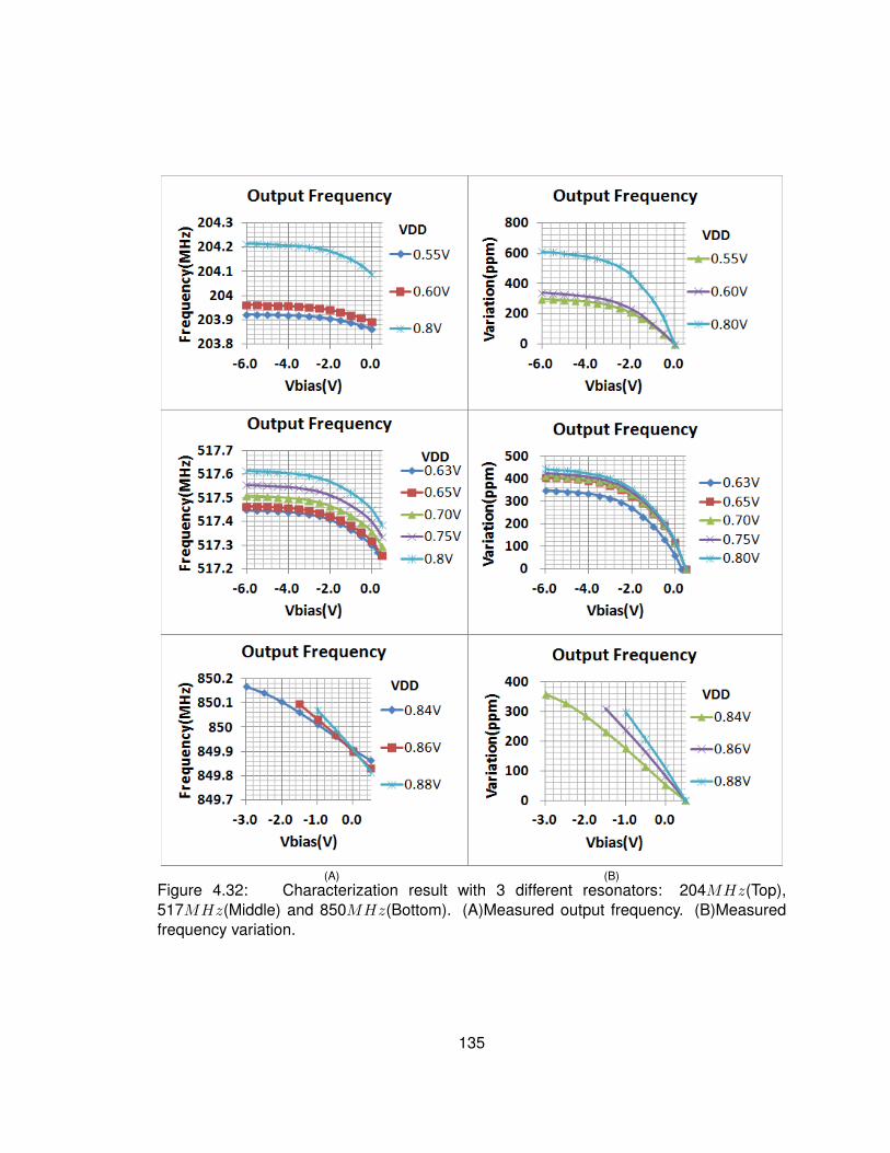
(A) (B)Figure 4.32: Characterization result with 3 different resonators: 204MHz(Top),517MHz(Middle) and 850MHz(Bottom). (A)Measured output frequency. (B)Measuredfrequency variation.
135

Table 4.3: Measured power consumption at different power supply.Frequency VDD(V) Current(µA) Power(µW )
0.55 85 47204MHz 0.60 240 144
0.80 965 7720.63 515 324
517MHz 0.70 658 4610.80 936 7490.84 1928 1620
850MHz 0.86 2227 19150.88 2488 2189
the power consumption will increase dramatically at higher supply voltages which is not
suitable for low power applications.
The phase noise of the oscillator, as shown in Figure 4.33, is measured by a spectrum
analyzer [108]. The oscillator demonstrates a better than -77dBc/Hz phase noise at
1kHz offset from the 204MHz center frequency. The phase noise partially comes from the
transistors in the sub-threshold region, which are very sensitive to power supply variations.
Due to the equipment’s limitation, the noise floor is measured to be -120dBc/Hz.
Discussion
In this work, a very low power multi-frequency tunable AlN CMR based oscillator is demon-
strated. Table. 4.4 compares the performance of the proposed work with other results in
the literature. Since all the MEMS resonators can be modeled using the MBVD model, the
circuit presented can be applied not only to the AlN CMR, but also to other types of MEMS
resonators. The frequency of the oscillator can be continuously adjusted by applying an
analog voltage on the varactor. However, the demonstrated tuning range is still limited.
One solution to extend the frequency range is to design multiple resonators with slightly
different resonant frequencies on the same substrate. Then, a switch connected to the
resonator array can selectively turn on one of the resonators to choose the desired fre-
quency. Another issue of AlN CMR is the temperature drift. For an uncompensated CMR
made of AlN thin films only, it suffers from a linear temperature coefficient of -20ppm/C
136

Figure 4.33: Measured phase noise of the 204MHz oscillator.
to -25ppm/C [116], which requires circuit level calibration to minimize this variation. The
demonstrated oscillator’s maximum frequency is 850MHz which is limited by the resonator.
As the process of fabricating AlN resonator matures, high frequency CMR resonating at
10GHz can be expected to come in the near future.
Table 4.4: Comparison of performances in literature.This work [109] [117]
MEMS CMR FBAR LBARFrequency(MHz) 204, 517, 850 1500 427Tuning Range(ppm) 611 200 810Supply Voltage(V) 0.55 2 NAPower 47µW@204MHz 1030µW 13mWIC Process 65nm 0.35µm 0.18µmPhase Noise(dBc/Hz)@1kHz -77, -73, -71 -86 -82
137

4.3.3. Clock and Data Recovery
Clock and data recovery (CDR) are commonly employed in multi-gigahertz serial links
where a dedicated clock signal doesn’t present and the serial data is seriously impaired
with loss and noise incurred jitter. CDR tries to recover the embedded clock from the in-
coming data stream and use the recovered clock to sample at the middle of the data period
such that the bit error is minimized. The IEEE 803.3ba standard requires the design to tol-
erate 0.62UI of total input jitter with ±100ppm frequency offset from the 10Gb/s incoming
data stream which means a CDR must be incorporated in the design. This work employs
a master-slave CDR topology as shown in Figure 4.34. The master CDR is a second or-
Phase Detector
LoopFilter
Phase InterplarotVCO
DATA IN10Gbps
DATA OUT
CLK OUT
UP/DOWN
Phase Detector
LoopFilter
Phase Interplarot
Phase Interpolator
DATA IN10Gbps
Master CDR
DATA OUT
CLK OUT
UP/DOWN
5GH
z C
LK
IN(F
rom
MC
DR
)
Master-Slave CDR System Diagram
Slave CDR
To other Slave CDRs
Clock buffer
(C)
Figure 4.34: Master-slave CDR top level diagram.
der PLL (phase locked loop) which can track both the frequency and phase of the input
138

data. A 10GHz LC tank VCO, controlled by the loop filter, generates the sampling clocks
used by both the master and slave CDRs. Since the sampling clock is already frequency
locked to the input data, the slave CDR only needs to track the phase error which implies
the VCO is no longer required. The result slave CDR is a first order PLL based on phase
picking scheme where the VCO is replaced by a phase interpolator (PI) whose transfer
function doesn’t have a pole. In this way, huge power and area savings can be achieved
by eliminating the VCO in 3 slave CDRs.
A full digital bang-bang CDR [118] topology is used for both CDRs. Instead of doing full
rate data slicing, a half rate architecture is designed. In this architecture, quadrature phase
clocks at 5GHz are used to sample the date as depicted in Figure 4.35. The four quadra-
0°
90°
180°
270°
IP
QP
IN
QN
EVEN ODD
E0 E2 E4E1 E3
10Gb/s Data
1 UI
5GHz Quadrature
clock
Figure 4.35: Half rate bang-bang CDR timing diagram.
ture phase clocks, generated from the 10GHz VCO output by a divider, are spaced 90
from each other. In the digital phase detector (PD), data is sampled on the rising edge
of each clock (E0 − E4). Ideally, E0 and E2 should be aligned to the middle of the data
eye for maximum jitter tolerance. However, due to jitter, the edges may come early or late
compared to their ideal positions as given in Figure 4.35. The sampling results are then
combined and decoded to determine the phase relationship between data and clock. The
output of PD is the digital bits “UP” and “DOWN” indicating whether the clock is coming
early or late than the ideal sampling point of data [119]. Next, the “UP” and “DOWN” signals
are processed by a programmable digital loop filter to get rid of any unwanted high frequen-
139

cy noise. Finally, the filter’s output controls either the VCO or PI to move the clock phase
back to its ideal position. In the master CDR, the loop filter’s digital output is connected to
a DAC which generates the required analog tuning voltage for VCO.
This design benefits from the whole digital implementation in the following aspects. First
and for most, the reduction of clock frequency to 5GHz makes it possible to replace the
CML circuit with CMOS logic as mentioned in Section 4.3.1. This accounts for large area
and power savings. Second, the digital loop filter eliminating the need for analog charge
pump and RC filter which usually occupy larger die area and are more sensitive to PVT
fluctuations. The filter’s coefficient is also easily adjusted. Third, the supply voltage can
be scaled with process due to its digital nature which contributes to further power saving.
Fourth, migration to other process is much easier for digital circuit.
Phase Detector
The block diagram of the phase detector in this work is shown in the bottom of Figure 4.36.
Compared with a traditional PD design which employs CML circuit, the slicer and decoder
CML to CMOS DFF Slicer50ohm Termination
CML Slicer50ohm Termination
DATA IN10Gbps
DATA IN10Gbps
CML Decoder
CMOS Decoder
UP/DOWN
UP/DOWN
DATA OUT
DATA OUT
Phase Detector
Figure 4.36: Phase detector design: using CML logic (top) and using CMOS logic (bottom).
are all designed with CMOS logic. A CML to CMOS converter is inserted between the
termination network and the slice to translate the input signal, usually in CML domain, into
rail-to-rail CMOS domain. The slicer is a dynamic D flip-flop (DFF) built with transmission
gate inverter (TG-inv) as given in Figure 4.37. In TG-inv, when CLK is high, the input, D,
is sampled on the parasitic capacitance C1 through transmission gate TG1. When CLK
140

CLK
D
CLK
QC1 C2
TG1 TG2INV1 INV2
Figure 4.37: Dynamic D flip-flop built with transmission gate inverter.
goes low, TG1 is open and TG2 is closed. Voltage stored on C1 propagates to C2 with
reverse polarity. The overall function is an falling edge triggered DFF. The loading capaci-
tance on clock and input signals are larger in TG-inv than those in TSPC (true single phase
clocked) [120] DFF. Thus, TSPC can operate faster due to its smaller input capacitance and
single phase clock operation. However, the differential clock in TG-inv is preferred for this
work because it can balance the loadings on the clock lines driven by CMOS buffers. In
the half rate bang-bang CDR, the 90 phase difference should be strictly maintained. Any
loading unbalance could lead to clock skew and hence degrade the jitter tolerance.
On the down side, TG-inv based slicer may introduce data dependent jitter. Because
of process variation and mismatch, the setup time of TG-inv DFF could be different for
sampling ‘1’ and ‘0’. Same thing also happens to hold time. These difference may affect
the loop’s dynamic behavior to adjust the clock phase and introduce unwanted jitter. In
addition, the large setup and hold time increases the metastability region and eat up the
jitter budget. Power supply noise introduced jitter is another concern for TG-inv DFF.
Phase Interpolator
Half rate phase picking CDR requires multiple clock phases over 2-UI period (360) to track
the input data’s phase change. Multi-phase clocks can be generated from cascaded delay
lines or through phase interpolation. In this work, 60 phases over 2-UI period is needed
because of the tight jitter budget. Due to its large delay limited by the delay cell, delay line
based topology can not provide the required time resolution. Thus, the phase interpolation
method utilizing a switched differential pair array is implemented [121].
This PI, as shown in Figure 4.38, works by summing the currents, controlled by two dif-
141

INIP QP QN
OUTP
OUTN
VDD
ITOT
IIP IQP
RR
C C
Figure 4.38: Circuit diagram of the phase interpolator.
ferential input clock pairs (IP − IN and QP − QN ) with different phases as illustrated in
Figure 4.35, on the output nodes. The total current, flowing through the load R and C,
creates the final output voltage. The output signal’s phase is between IP and QP and can
be adjusted by the change the weighting between IIP and IQP where ITOT = IIP + IQP .
For example, if IIP = ITOT , the output phase is only determined by IP − IN ; if now
IQP = ITOT , the output phase is shifted by 90 compared to the IIP = ITOT case.
To generate linearly spaced phase output, the ideal input of PI should be a triangle wave
as illustrated in Figure 4.39. Thus, the transition of the rail-to-rail clock from master CDR
must be “slowed down” which in this work is achieved by adding excessive RC to the
PI’s input. In addition, since the output of PI is a CML signal, a CML to CMOS converter
must be utilized to translate the output to full swing CMOS signal and buffer them to the PD.
During the conversion, the signal’s rising and falling edge might be distorted due to process
mismatch and environment condition. If the differential relationship between OUTP and
OUTN is not maintained, the TG-inv relying on these clocks may enter a race condition.
Thus, an AC coupled differential with cross-couple skew cells are added after the CML to
CMOS converter as illustrated in Figure 4.40.
PI shown in Figure 4.38 only interpolates between one quadrature, that is, 90. To cover
142

0 5 10-1
0
1Sine wave
θ(rad)
Am
plit
ud
e
0 5 10-1
0
1Triangle wave
θ(rad)
Am
plit
ud
e
0 5 10-1
0
1Square wave
θ(rad)
Am
plit
ude
0 2 4 60
0.2
0.4
0.6
0.8
Square wave with RC
θ(rad)
Am
plit
ude
Figure 4.39: Phase interpolator’s output with different input waveform. Bold red curveis input IP . Bold green curve is input QP . Thin blue curve is the output signal afterinterpolation.
INP
INN
OUTP
OUTN
CMOS Duty Cycle Correction
Figure 4.40: Clock buffer and duty cycle correction.
143

the full 360 range, which is 2-UI period, input selection multiplexer (MUX) must be added
before the input. Because MUX control and weighting control signals are generated by
asynchronous clock from the loop filter, there might be phase jumps on the output during
the quadrature switching. Thus, the sequence and timing of these control signals must
be properly design to avoid this issue. The simulated 60 phase step and DNL (differential
non-linearity) are plotted in Figure 4.41.
0 20 40 600
100
200
300
400Phase Shift vs Control Code
Control code
Ph
ase
Shi
ft(D
eg)
IdealSimulated
0 20 40 60-0.6
-0.4
-0.2
0
0.2
0.4Phase Shift DNL
Control codeD
NL
(LS
B)
Simulated
(A) (B)
Figure 4.41: (A)Simulated phase step. (B)DNL of phase step.
4.4. Measurement Result
The measurement results of the optical transmitter system incorporating the previously
described optimizations are presented in this section. As introduced in Section 4.3.1, two
transmitters are developed focusing on different performances aspects:
1. The first system is a 40Gb/s serial (OOK) transmitter with emphasis on the speed
improvement.
2. The second system is a 40Gb/s PAM-16 transmitter with emphasis on the power
efficiency enhancement.
The electrical driver IC and optical modulator IC are fabricated in standard 40nm CMOS
and 0.13µm SOI CMOS process, respectively. The photograph of the 40Gb/s serial trans-
mitter, composed of both ICs, is shown in Figure 4.42 [65]. Two ICs are put right next to
144

each other and connected through gold bond wires with 60µm in diameter and 800µm in
length. The driver IC on the top is measured about 2.6mm×1.8mm. The optical IC on
the bottom is measured about 2.6mm×1.5mm. The SISCAP MZM in this config features
a total RF length of 480µm and occupies a silicon area of about 0.18mm2. The die size
and other major building blocks of the 40Gb/s PAM-16 transmitter are similar to that of the
OOK transmitter. Only the driver and SISCAP sections are modified for the segmented
configuration in the PAM-16 transmitter.
Figure 4.42: Chip photograph of the 40Gb/s serial (OOK) optical transmitter: electricaldriver IC (top) in 40nm CMOS and optical modulator IC in 0.13µm SOI CMOS (bottom).
4.4.1. Test Setup
The test setup to evaluating the transmitter performance is given in Figure 4.43. The major
focus of this setup is on the optical eye characteristics measurement. For the other param-
eters such as input return loss, CDR jitter tolerance, and BER, different configurations are
implemented.
This setup consists of three major signal paths as marked with different colors in Figure 4.43.
145

Figure 4.43: Measurement setup of the optical transmitter for both 40G/s serial and PAM-16 operation.
In the electrical path, the FPGA board generates 4×10Gb/s input data streams and sends
them to the master-slave CDR on the driver IC. The data stream can be programmed to
different patterns like PRBS7, PRBS31, high frequency 01 alternation, low frequency al-
ternation (multiple 0s and multiple 1s in consecutive), and etc. The reference clock of the
CDR comes from an external signal source which can later be replaced by an inexpen-
sive crystal oscillator. Various equipments are connected to the DUT (device under test)
to monitor the laser power and bias conditions. The the modulator’s optical output is cap-
tured by a high speed oscilloscope with a 40GHz optical plug-in module to convert light
signal back into electrical signal. Along the optical path, a temperature controlled CW laser
source provides the input of the SISCAP MZM. A polarization rotator is inserted between
the laser source and the MZM to adjust the electric field’s angle. The maximum modulation
efficiency can be achieved when the electric field of the laser is lined up with the electrical
field generated by the modulator’s driving voltage. A close look of the setup in the DUT re-
146

Driver IC
MZM
CAD Drawing
Figure 4.44: A close look of the setup in the DUT region.
gion is drawn in Figure 4.44. Laser, going through a single-mode fiber (SMF), needs to be
coupled in and out of the modulator which is a nontrivial task in practice. This is because
the cross section of the on-chip optical waveguide is very small, typically less than a few
micron in both directions. Several techniques can be implemented to realize the coupling
which include grating coupling, butt coupling, end-fire coupling, and prism coupling [85].
Since the coupling loss is not a major concern, the butt coupling method is implemented
in this work due to its simple form. In Figure 4.44, the fiber core is first moved to touch
the edge of the optical die, and then aligned to the silicon waveguide. However, since
there is no solid connections between the fiber and the waveguide, this coupling method is
quite sensitive to any mechanical noise introduced by the surrounding environment. The
situation is worse in the vertical direction because the optical mode only overlaps with the
free carrier modulation region for tens of nanometers as explained in Chapter 3. Thus,
the DUT as well as the other equipments are put on an optical table to isolate any kinds
147

of vibrations. Even with the optical table, the mechanical noise still can’t be completely
removed. For example, the air flow around the DUT and moving parts such as heat sink
fan inside the equipment can both shift the fiber back and forth. These noise factor must
be considered when examining the result. The alignment of fiber to the silicon waveguide
is achieved through a 3-axis stage controlled by piezoelectric actuators which has the
required nanometer accuracy in the vertical direction.
4.4.2. Characterization Result
Eye Diagram
The 40Gb/s serial transmitter is first characterized. In the test, the eye diagram only shows
20Gb/s data rate as plotted in Figure 4.45 [65] instead of the desired 40Gb/s. There is
Figure 4.45: Measured OOK modulation eye diagram showing 20Gb/s with large duty-cycle distortion.
also a large duty-cycle distortion observed in the optical eye with PRBS31 input pattern.
Further investigation shows the expected 20GHz clock for the final serializer stage doesn’t
come out properly. After increasing the supply voltage by 20%, the 20GHz clock appears
but its jitter is too big that the optical eye is completely closed. After some tests, this issue
is identified to be a circuit bug in the frequency doubler. Due to mismatch and process
variation, a DC term appears at the input of the XOR (exclusive or) gate in Figure 4.26
which causes the XOR gate to saturate and makes the input 10GHz clock override the
148

20GHz signal. The offset voltage also introduces the duty-cycle distortion. Increasing
supply voltage can mitigate this issue. However, as the supply voltage becomes higher,
the bias point of the other blocks may get affected which leads large jitter. The issue
was not catched during the design phase because the mismatch effect was overlooked.
Although the issue related to the frequency doubler requires the driver to operate at a
voltage 20% higher than it was designed for, this is the highest speed demonstration of a
CMOS photonic MZM ever reported.
(A)
(B)Figure 4.46: Measured PAM-4 modulation eye diagram . (A)Without average in the scopesettings. (B)With average in the scope settings.
The PAM-4 and PAM-16 optical eye diagrams with 17GHz optical filter enabled in the
oscilloscope are then measured as shown in Figure 4.46 and Figure 4.47, respectively [65].
149

For PAM-4 modulation, the eye diagram indicates the transmitter can achieve an error free
data rate of 20Gb/s. The optical eye is wide and open for each level.
(A)
(B)
Figure 4.47: Measured PAM-16 modulation eye diagram. (A)DC level sweep. (B)Runningat 40Gb/s with bit errors due to eye closure.
In the DC level sweep test as shown in Figure 4.47(A), PAM-16 modulation demonstrates
16 equally spaced levels which behave like an optical DAC, a first time showcase of a
16-level segmented MZI, driven by an inverter based digital driver! The level separations
are equal which proves the enhanced binary code weighted PAM-16 scheme is working
properly.
Excessive optical noise is observed on the PAM-16 eye (Figure 4.47(B)) which may caused
by power supply noise and mechanical vibration of the fiber. This noise is also a result of
the wide bandwidth receiver that is optimized for OOK signals at higher data rates. Rise
150

and fall times captured from this plot are 48-54ps which is 50% higher than the simulation
result (30-33ps). We suspect this is caused by model inaccuracy - the parasitic capacitance
predicted by the model is smaller than the real value. The reason leads to this discrepancy
is still under investigation. To resolve this issue, the driver size can be increased to tolerate
the larger loading capacitance.
Extinction Ratio The extinction ratio measurement result in PAM-16 is shown in Figure 4.48.
The expected ER for this work is around 7dB. The measured results show the extinction
Figure 4.48: ER measurement result of the PAM-16 transmitter.
Ratio is around 7.4dB in both cases.
Power Consumption For the 40Gb/s OOK transmitter, although the eye is closed due to
excessive jitter after increasing the supply, the power consumption data is still valid since
all the internal logics are still toggling at the correct frequency. Operating at 40Gb/s with
PRBS31 pattern, the modulation power of the OOK transmitter is 160mW (4pJ/bit). When
the data rate is reduced to 20Gb/s, the modulation power becomes 90mW (4.5pJ/bit).
The 40Gb/s PAM-16 circuit consumes 10mW of power with PRBS31 pattern. This trans-
lates to 250fJ/bit which is the lowest power reported for an MZM at this speed. When
configured to PAM-4 with 20Gb/s data rate, the modulation power is 5.8mW (0.29pJ/bit).
151

Power consumptions for the entire transmit data path including CDR, MZI and CW laser
(complete transmit solution) are 480mW (error free OOK at 20Gb/s) and 446mW (error
free PAM-4 at 20Gb/s).
These performance data is summarized in Table 4.5.
Table 4.5: Performance summary of the two optical transmittersData Rate 20Gb/s 20Gb/s 40Gb/s 40Gb/sModulation Scheme OOK PAM-4 OOK PAM-16Pattern PRBS31 PRBS31 PRBS31 PRBS31Rise/Fall(10%-90%) 25ps 50ps – 48psModulation Energy 4.5pJ/bit 0.29pJ/bit 4pJ/bit 0.25pJ/bitTotal Power 480mW 446mW 550mW 450mW
CDR On the CDR measurement, the jitter tolerance has not been fully characterized yet
due to lack of parallel BERT equipments. However, the transmitter runs over night with no
errors with its input connected to a four channel PRBS31 pattern generator through a 30
inch long coaxial cable. The PI’s control code, monitored via the test bus, exhibits a dither-
ing behavior after lock, which proves the phase picking master-slave CDR is functioning.
The measured power consumption of a single slave CDR is 18mW . The master CDR
consumes 71mW power where the added power mainly comes from the LC tank VCO.
4.5. Summary
This chapter focuses on the transmitter performance enhancement. Among all characteri-
zation parameters, power reduction and speed improvement are the first to be considered.
Then, the optimization methods are discussed on optical modulator and electrical driver
separately.
For the optical modulator, reducing the size can help with the bandwidth. However, trade-
offs must be made among various parameters determined by the specific application. To
reduce the power consumption, a PAM-16 modulation scheme is proposed. Different im-
plementations of PAM-16 are also compared. The enhanced binary code weighted PAM-
16, which has the best output linearity, is finally chosen for this work. A focal plane wire
152

grid image sensor capable of extracting polarization information is proposed. The mea-
sured performance is good in visible wavelength range. Our simulation result also shows
it has better PER performance in the communication wavelength range.
On the electrical driver side, similar analysis is carried out on power and speed in both
system architecture level and key building blocks level. A master-slave CDR structure is
selected to recover the input data impaired by jitter. Phase picking scheme is utilized in the
slave CDR design to further save power. A tunable MEMS based oscillator is developed
as a show case whose power consumption is reduced significantly.
Finally, the evaluation results of the two proposed optical transmitters are presented. One
design bug in the frequency doubler is identified. Measurement results show the transmit-
ters are running error free at 20Gb/s for both OOK and PAM-4 modulation schemes. The
power consumption meets our design target.
153

CHAPTER 5 : Conclusion and Future Works
5.1. Summary
The need for more bandwidth driven by streaming video and other data intensive applica-
tions has been steadily pushing the optical link speed to the 40Gb/s and 100Gb/s domain.
Compared to a VCSEL or a ring resonator, a Mach-Zehnder Interferometer (MZI) modu-
lator is the best solution for long distance (greater than 500m), high data rate (faster than
28Gb/s) optical communications. However, high power consumption, low link density and
high cost seriously prevent traditional MZI from being the next generation of optical link
technology.
To fundamentally reduce the cost of MZI, it is highly desirable to make the process C-
MOS compatible with high efficiency, thus the modulation voltage, size, and power can be
reduced to a level where advanced sub-1V CMOS circuits can be used as the driver.
To address the existing issues, this research proposes for the first time two silicon photonic
MZI based optical transmitters, working with two modulation schemes: OOK or config-
urable PAM-N (N=4, 16), featuring 20Gb/s data rate and sub-pJ/bit modulation energy
(PAM-4) using only 1V supply. The fully CMOS compatible photonic device is highly cost-
effective in terms of integration, manufacturability and scalability.
The optical modulator is based on the patented SISCAP technology from CISCO System-
s. Most of the work on the circuit design and the characterization was done at CISCO
(formerly Lightwire) in Allentown, PA as part of the SERDES group. Compared with oth-
er silicon photonic modulator devices, such as MZI made with MOSCAP structure, P-i-N
junction and the PN junction MZI, SISCAP operates in both depletion and accumulation
region, moving a lot more free carriers at a given voltage. In addition, the concentration
region of free carriers overlaps with maximum of the optical mode. Thus, the efficiency of
SISCAP is at least a factor 10 higher than other types of MZI.
154

After reviewing of optical modulator’s history, fundamental properties and principles of op-
erations in Chapter 2, the thesis focuses on the creation of an accurate circuit model of the
SISCAP MZM. This model enables the co-simulation and optimization of optical modula-
tors with the electrical driver using commercially available EDA tools. With the help of this
model, the modulator’s behaviors can be predicted and potential design and performance
issues can be found in the early stage of the design. Thus, the design cycle as well as the
NRE (non-recurring engineering) cost can be dramatically reduced.
To meet the performance target on power consumption and modulation speed, both the
optical modulator and the electrical driver are extensively optimized. On the optical side,
PAM-16 modulation scheme is proposed. Technique to improve the PAM-16 output linearity
is also presented. A focal plane wire grid image sensor capable of extracting polarization
information is also demonstrated. On the electrical driver side, power saving and speed
boosting is achieved through careful architecture selection in both system level and block
level.
The driver IC and optical modulator are fabricated in 40nm CMOS and 0.13µm SOI CMOS
process, respectively. The MZI modulator features a total RF length of 480µm and occu-
pies a silicon area of 0.18mm2. The measured OOK optical eye demonstrates an error free
data rate up to 20Gb/s. The PAM-4 and PAM-16 optical eye as well as the equally-spaced
DC optical levels for the PAM-16 are successfully demonstrated. The PAM-4 demonstrates
an error free data rate of 20Gb/s. Due to electrical and mechanical noise, PAM-16 eye is
partially closed at 40Gb/s.
Operating with PRBS31 pattern, the modulation power at 20Gb/s is 90mW (4.5pJ/bit) for
OOK and 5.8mW (0.29pJ/bit) for PAM-4 which are the lowest reported in literature for
silicon photonic MZI modulator. Power consumptions for the entire transmit data path in-
cluding CDR, MZI and CW laser (complete transmit solution) are 480mW (OOK at 20Gb/s)
and 446mW (PAM-4 at 20Gb/s).
155

5.2. Future Work
There are some issues found during the lab characterization of the proposed transmitter.
The electrical driver IC had a design bug in the DLL that generated 20GHz signal causing
the 40Gb/s output to be jittery and with duty cycle distortion. In future revisions, this bug
could be fixed and the real 40Gb/s performance can be measured. Rise and fall times of
PAM-16 are 48-54ps which is 50% higher than the simulation result (30-33ps). We suspect
this is caused by model inaccuracy - the parasitic capacitance predicted by the model is
smaller than the real value. The reason for this discrepancy is still under investigation.
More lab measurements and simulations with existing models are required to correlate the
results and identify the root cause of this discrepancy. In addition, the CDR performance
has not been fully characterized yet due to lack of parallel BERT equipments.
For future development, the model of the optical device can be extended to include the
schematic design, simulation, automatic layout generation, DRC (design rule check) and
LVS (layout versus schematic) which forms a fully functional optical PDK (process design
kit). The traveling wave matching can be further investigated. The phase modulation of
SISCAP can also be explored to construct QPSK modulators. By combining the PAM-N
and phase modulator, advanced modulation schemes such as QAM-N can also be real-
ized.
156

BIBLIOGRAPHY
[1] CISCO Systems, “Cisco visual networking index: Forecast and methodology, 2011-2016,” [Online]. Available: http://www.cisco.com/en/US/solutions/collateral/ns341/ns525/ns537/ns705/ns827/white paper c11-481360 ns827 Networking SolutionsWhite Paper.html, May 2012.
[2] A. Gara, “Supercomputing’s symbiotic relationship with advanced optics,” [Online].Available: http://www.ofcnfoec.org/osa.ofc/media/Default/PDF/2011/2011PlenaryGara.pdf, May 2011.
[3] IBM, “Roadrunner super computer,” [Online]. Available: http://www.top500.org/system/9485, June 2008.
[4] Fujitsu, “K super computer,” [Online]. Available: http://www.top500.org/lists/2011/06/highlights, June 2011.
[5] B. Offrein, “Optical interconnects for computing applications,” in IEEE PhotonicsConference (IPC), 2012, pp. 183–184.
[6] A. L. Schawlow and C. H. Townes, “Infrared and optical masers,” in Physics Review,vol. 112, no. 6, 1958, pp. 1940–1949.
[7] D. A. Kidd, Collins Gem Latin Dictionary. HarperCollins Publishers, 1996.
[8] NASA, “WHERE ARE THE VOYAGERS?” [Online]. Available: http://voyager.jpl.nasa.gov/where/index.html, Apr 2013.
[9] S. Damaraju, V. George, S. Jahagirdar, T. Khondker, M. R., S. Sarkar, S. Scott, S. I.,and A. Subbiah, “A 22nm IA multi-CPU and GPU System-on-Chip,” in ISSCC Dig.Tech. Papers, 2012, pp. 56–57.
[10] J. Yin, J. Ren, and H. Lu, “Quantum teleportation and entanglement distribution over100-kilometre free-space channels,” in Nature, vol. 488, 2012, pp. 185–188.
[11] A. Einstein, “On the Electrodynamics of Moving Bodies,” in Annalen der Physik,vol. 17, 1905, p. 891.
[12] IEEE, “IEEE P802.11ac/D5.0,” [Online]. Available: http://www.techstreet.com/ieee/products/1827366, Jan 2013.
[13] Gartner, “Gartner Says Worldwide PC, Tablet and Mobile Phone Combined Ship-ments to Reach 2.4 Billion Units in 2013,” [Online]. Available: http://www.gartner.com/newsroom/id/2408515, Apr 2013.
[14] ITRS, “INTERNATIONAL TECHNOLOGY ROADMAP FOR SEMICONDUCTORS2006 UPDATE FRONT END PROCESSES,” [Online]. Available: http://www.itrs.net/Links/2006Update/FinalToPost/07 FEP2006Update.pdf, 2006.
157

[15] J. P. Reynard, C. Verove, E. Sabouret, P. Motte, B. Descouts, C. Chaton, J. Michailos,and K. Barla, “Integration of Fluorine-doped Silicon oxide in copper pilot line for0.12µm technology,” in Microelectronic Engineering, vol. 60, no. 1, Jan 2002, pp.113–118.
[16] C. S. Yang, Y. H. Yu, K.-M. Lee, H.-J. Lee, and C. K. Choi, “Investigation of low dielec-tric carbon-doped silicon oxide films prepared by PECVD using methyltrimethoxysi-lane precursor ,” in The Joint Meeting of 7th APCPST, vol. 506, no. 0, 2006, pp.50–54.
[17] Q. Han, W. Chen, C. Waldfried, O. Escorcia, N. Sbrockey, T. Bridgewater, E. Moyer,and I. Berry, “Ultra low-k porous silicon dioxide films from a plasma process,” inProceedings of the IEEE 2001 International Interconnect Technology Conference,2001, pp. 171–173.
[18] IEEE, “IEEE P802.3bj 100 Gb/s Backplane and Copper Cable Task Force ChannelData,” [Online]. Available: http://www.ieee802.org/3/100GCU/public/channel.html,Apr 2011.
[19] J. Sonntag, J. Stonick, J. Gorecki, B. Beale, B. Check, X.-M. Gong, J. Guiliano,K. Lee, B. Lefferts, D. Martin, U.-K. Moon, A. Sengir, S. Titus, G.-Y. Wei, D. Weinlad-er, and Y. Yang, “An adaptive PAM-4 5Gb/s backplane transceiver in 0.25µm CMOS,”in Proceedings of the IEEE Custom Integrated Circuits Conference, 2002, pp. 363–366.
[20] B. Zhu, T. Taunay, M. Fishteyn, X. Liu, S. Chandrasekhar, M. F. Yan, J. M. Fini,E. M. Monberg, and F. V. Dimarcello, “112-Tb/s Space-division multiplexed DWDMtransmission with 14-b/s/Hz aggregate spectral efficiency over a 76.8-km seven-corefiber,” in Optical Express, vol. 19, no. 17, 2011, pp. 16 665–16 671.
[21] X. Zhou, L. E. Nelson, P. Magill, B. Zhu, P. Borel, D. Peckham, and K. Carlson,“12,000km Transmission of 100GHz Spaced, 8x495-Gb/s PDM Time-Domain HybridQPSK-8QAM Signals,” in Optical Fiber Communication Conference/National FiberOptic Engineers Conference 2013, 2013, p. OTu2B.4.
[22] J. Hecht, City of Light: The Story of Fiber Optics. New York: Oxford UniversityPress, 1999.
[23] A. Einstein, “On the Quantum Theory of Radiation,” in Physikalische Zeitschrift,vol. 18, 1917, pp. 121–128.
[24] R. N. Hall, G. E. Fenner, J. D. Kingsley, T. H. Soltys, and R. O. Carlson, “Coherentlight emission from GaAs junctions,” in Physical Review Letters, vol. 9, no. 9, 1962,pp. 366–368.
158

[25] K. M. Johnson, “High-speed photodiode signal enhancement at avalanche break-down voltage,” in IEEE Transactions on Electron Devices, vol. 12, no. 2, 1965, pp.55–63.
[26] N. Bloembergen, P. S. Pershan, and L. R. Wilcox, “Microwave modulation of light inparamagnetic crystals,” in Physical Review Letters, vol. 120, no. 6, 1960, pp. 2014–2023.
[27] F. P. Kapron, D. B. Keck, and R. D. Maurer, “Radiation losses in glass optical waveg-uides,” in Applied Physics Letters, vol. 17, no. 11, 1970, pp. 423–425.
[28] H. Murata and N. Inagaki, “Low-loss single-mode fiber development and splicingresearch in Japan,” in IEEE Journal of Quantum Electron., vol. QE17, no. 6, 1981,pp. 835–849.
[29] E. Desurvire, J. Simpson, and P. Becker, “High-gain erbium-doped traveling-wavefiber amplifier,” in Optics Letters, vol. 12, no. 11, 1987, pp. 888–890.
[30] J. A. Kash, A. Benner, F. E. Doany, D. Kuchta, B. G. Lee, P. Pepeljugoski, L. Schares,C. Schow, and M. Taubenblatt, “Optical Interconnects in Future Servers,” in OpticalFiber Communication Conference/National Fiber Optic Engineers Conference 2011,2011, p. OWQ1.
[31] K. Schuh, B. Junginger, E. Lach, W. Idler, G. Veith, S. Vorbeck, M. Schneider-s, P. Wagner, D. Werner, H. Haunstein, D. Breuer, R.-P. Braun, M. Paul, andA. Ehrhardt, “8x10⁷ Gbit/s NRZ-VSB DWDM Field Transmission over 500 km SSMF,”in ITG Symposium on Photonic Networks, 2009, pp. 1–4.
[32] R.-P. Braun, “100gbit/s ip-router and dwdm transmission interoperability field tests,”in ITG Symposium on Photonic Networks, 2011, pp. 1–3.
[33] C. Gutierrez-Martinez, “Analog TV transmission via optical fiber using PWM-subcarrier,” in Proceedings of the 33rd Midwest Symposium on Circuits and Sys-tems, vol. 2, 1990, pp. 804–807.
[34] P. J. Winzer, “Modulation and Multiplexing in Optical Communication Systems,” [On-line]. Available: http://photonicssociety.org/newsletters/feb09/modulation.pdf, Feb2009.
[35] J. Sinsky, A. Adamiecki, L. Buhl, G. Raybon, P. Winzer, O. Wohlgemuth, M. Duelk,C. Doerr, A. Umbach, H. G. Bach, and D. Schmidt, “A 107-Gbit/s Optoelectronic Re-ceiver Utilizing Hybrid Integration of a Photodetector and Electronic Demultiplexer,”in Journal of Lightwave Technology, vol. 26, no. 1, 2008, pp. 114–120.
[36] M. Nakazawa, S. Okamoto, T. Omiya, K. Kasai, and M. Yoshida, “256-QAM (64 Gb/s)Coherent Optical Transmission Over 160 km With an Optical Bandwidth of 5.4 GHz,”in IEEE Photonics Technology Letters, vol. 22, no. 3, 2010, pp. 185–187.
159

[37] Y. Mori, C. Zhang, M. Usui, K. Igarashi, K. Katoh, and K. Kikuchi, “200-km transmis-sion of 100-Gbit/s 32-QAM dual-polarization signals using a digital coherent receiv-er,” in 35th European Conference on Optical Communication, 2009, pp. 1–2.
[38] J. Yu, X. Zhou, Y.-K. Huang, S. Gupta, M.-F. Huang, T. Wang, and P. Magill, “112.8-Gb/s PM-RZ-64QAM optical signal generation and transmission on a 12.5GHz WDMgrid,” in Optical Fiber Communication (OFC), collocated National Fiber Optic Engi-neers Conference, 2010 Conference on (OFC/NFOEC), 2010, pp. 1–3.
[39] A. Gnauck, P. Winzer, G. Raybon, M. Schnecker, and P. Pupalaikis, “10x224-Gb/sWDM Transmission of 56-Gbaud PDM-QPSK Signals Over 1890km of Fiber,” inIEEE Photonics Technology Letters, vol. 22, no. 13, 2010, pp. 954–956.
[40] C. E. Shannon, “A mathematical theory of communication,” in Bell System TechnicalJournal, 1948, pp. 379–423,623–656.
[41] J. R. Janesick, Photon Transfer DN→ λ. SPIE Press, 2007.
[42] K.-P. Ho, Phase-Modulated Optical Communication Systems. Springe, 2005.
[43] A. Yariv, Introduction to Optical Electronics, 2nd ed. New York: Holt, Rinehart andWinston, 1976.
[44] D. S. Chemla, T. C. Damen, D. A. B. Miller, A. C. Gossard, and W. Wiegmann,“Electroabsorption by Stark effect on room-temperature excitons in GaAs/GaAlAsmultiple quantum well structures,” in Applied Physics Letters, vol. 42, no. 10. AIP,1983, pp. 864–866.
[45] G. P. Agrawal, Fiber-Optic Communication Systems. John Wiley & Sons, Inc., 2010.
[46] D. A. B. Miller, D. S. Chemla, T. C. Damen, A. C. Gossard, W. Wiegmann, T. H.Wood, and C. A. Burrus, “Electric field dependence of optical absorption near theband gap of quantum well structures,” in Physical Review B, vol. 32, July 1985, pp.1043–1060.
[47] P. Basu, Theory of Optical Processes in Semiconductors: Bulk and Microstructures.Clarendon Press, Oxford, UK, 2003.
[48] B. Nag, Electron Transport in Compound Semiconductors. Springer, Berlin, 1980.
[49] S. Spector, C. Sorace, M. Geis, M. Grein, J. Yoon, T. Lyszczarz, E. Ippen, andF. Kartner, “Operation and Optimization of Silicon-Diode-Based Optical Modulators,”in IEEE Journal of Selected Topics in Quantum Electronics, vol. 16, no. 1, 2010, pp.165–172.
[50] H. Soda, K. ichi Iga, C. Kitahara, and Y. Suematsu1, “GaInAsP/InP Surface EmittingInjection Lasers,” in Japenese Journal of Applied Physics, vol. 18, 1979, pp. 2329–2330.
160

[51] J. Proesel, B. Lee, A. Rylyakov, C. Baks, and C. Schow, “Ultra-low-power 10 to 28.5Gb/s CMOS-driven VCSEL-based optical links [Invited],” in IEEE/OSA Journal ofOptical Communications and Networking, vol. 4, no. 11, 2012, pp. B114–B123.
[52] S. Kobayashi, Y. Yamamoto, M. Ito, and T. Kimura, “Direct Frequency ModulationIn AlGaAs Semiconductor Lasers,” in IEEE Transactions on Microwave Theory andTechniques, vol. 30, no. 4, 1982, pp. 428–441.
[53] S. Kobayashi, Y. Yamamoto, , and T. Kimura, “Frequency and phase modulationof semiconductor lasers,” in Topics in Lightwave Transmission Systems, 1991, pp.151–202.
[54] T.-H. Wu, J.-P. Wu, and Y.-J. Chiu, “Low-Power-Driven and Low-Optical-Loss 40-Gb/s Electroabsorption Modulator Using Self-Aligned Two-Step Undercut-EtchedWaveguide,” in IEEE Electron Device Letters, vol. 33, no. 7, 2012, pp. 1021–1023.
[55] C. Li, R. Bai, A. Shafik, E. Tabasy, G. Tang, C. Ma, C.-H. Chen, Z. Peng, M. Fiorenti-no, P. Chiang, and S. Palermo, “A ring-resonator-based silicon photonics transceiverwith bias-based wavelength stabilization and adaptive-power-sensitivity receiver,” inISSCC Dig. Tech. Papers, 2013, pp. 124–125.
[56] M. J. Deen and P. Basu, Silicon Photonics Fundamnetals and Devices. John Wiley& Sons, Inc., 2012.
[57] F. Koyama and K. Iga, “Frequency chirping in external modulators,” in Journal ofLightwave Technology, vol. 6, no. 1, Jan 1988, pp. 87–93.
[58] A. Liu, L. Liao, D. Rubin, H. Nguyen, B. Ciftcioglu, Y. Chetrit, N. Izhaky, and M. Pan-iccia, “High-speed optical modulation based on carrier depletion in a silicon waveg-uide,” in Optical Express, vol. 15, no. 2, Jan 2007, pp. 660–668.
[59] N.-N. Feng, S. Liao, D. Feng, P. Dong, D. Zheng, H. Liang, R. Shafiiha, G. Li, J. E.Cunningham, A. V. Krishnamoorthy, and M. Asghari, “High Speed Silicon Carrier-Depletion Mach-Zehnder Modulator with 1.4V-cm VπL,” in Integrated Photonics Re-search, Silicon and Nanophotonics and Photonics in Switching. Optical Society ofAmerica, 2010, p. IMB3.
[60] G. V. Treyz, P. May, and J.-M. Halbout, “Silicon optical modulators at 1.3µm basedon free-carrier absorption,” in IEEE Electron Device Letters, vol. 12, no. 6, 1991, pp.276–278.
[61] C. Tang and G. Reed, “Highly efficient optical phase modulator in SOI waveguides,”in Electronics Letters, vol. 31, no. 6. IET, 1995, pp. 451–452.
[62] A. Liu, R. Jones, L. Liao, D. Samara-Rubio, D. Rubin, O. Cohen, R. Nicolaescu,and M. Paniccia, “A high-speed silicon optical modulator based on a metal-oxide-semiconductor capacitor,” in Nature, vol. 427, Feb 2004, pp. 615–618.
161
[63] J. Basak, L. Liao, A. Liu, D. Rubin, Y. Chetrit, H. Nguyen, D. Samara-Rubio, R. Co-hen, N. Izhaky, and M. Paniccia, “Developments in Gigascale Silicon Optical Modu-lators Using Free Carrier Dispersion Mechanisms,” in Advances in Optical Technolo-gies, 2008.
[64] D. D‘Andrea, “CMOS Photonics Today and Tomorrow Enabling Technolo-gy,” [Online]. Available: http://www.ofcnfoec.org/osa.ofc/media/Default/PDF/2009/09-Dandrea.pdf, Sept 2009.
[65] X. Wu, B. Dama, P. Gothoskar, P. Metz, K. Shastri, S. Sunder, J. Van der Spiegel,Y. Wang, M. Webster, and W. Wilson, “A 20Gb/s NRZ/PAM-4 1V transmitter in 40n-m CMOS driving a Si-photonic modulator in 0.13µm CMOS,” in ISSCC Dig. Tech.Papers, 2013, pp. 128–129.
[66] K. Shastri, “CMOS Photonics,” in 2009 Asia Communications and Photonics Confer-ence and Exhibition (ACP), nov. 2009, pp. 1–2.
[67] M. Watts, W. Zortman, D. Trotter, R. Young, and A. Lentine, “Low-Voltage, Compact,Depletion-Mode, Silicon Mach-Zehnder Modulator,” in IEEE Journal of Selected Top-ics in Quantum Electronics, vol. 16, no. 1, 2010, pp. 159–164.
[68] Q. Xu, S. Manipatruni, B. Schmidt, J. Shakya, and M. Lipson, “12.5 Gbit/s carrier-injection-based silicon micro-ring silicon modulators,” in Optical Express, vol. 15,no. 2. OSA, Jan 2007, pp. 430–436.
[69] X. Zheng, J. Lexau, Y. Luo, H. Thacker, T. Pinguet, A. Mekis, G. Li, J. Shi, P. Amberg,N. Pinckney, K. Raj, R. Ho, J. E. Cunningham, and A. V. Krishnamoorthy, “Ultra-low-energy all-CMOS modulator integrated with driver,” in Optical Express, vol. 18, no. 3,Feb 2010, pp. 3059–3070.
[70] Chelsio, “T4 Unified Wire Adapters,” [Online]. Available: http://www.chelsio.com/nic/t4-unified-wire-adapters/.
[71] A. Larsson, “Advances in VCSELs for Communication and Sensing,” in IEEE Journalof Selected Topics in Quantum Electronics, 2011, pp. 1–17.
[72] Addoncomputer, “X2-10G-MMF-AO 10GBASE X2 Transceiver,” [Online]. Available:http://www.addoncomputer.com/data sheets/X2-10GB-LRM-AO.pdf.
[73] D. Marris-Morini, L. Vivien, G. Rasigade, J.-M. Fedeli, E. Cassan, X. Le Roux,P. Crozat, S. Maine, A. Lupu, P. Lyan, P. Rivallin, M. Halbwax, and S. Laval, “Re-cent Progress in High-Speed Silicon-Based Optical Modulators,” in Proceedings ofthe IEEE, vol. 97, no. 7, 2009, pp. 1199–1215.
[74] U. Berkeley, “The Spice Page,” [Online]. Available: http://bwrcs.eecs.berkeley.edu/Classes/IcBook/SPICE/, 2013.
162

[75] M. Ghiron, P. Gothoskar, R. K. Montgomery, V. Patel, S. Pathak, K. Shastri, andK. A. Yanushefski, “High speed silicon-based electro-optic modulator,” US PatentUS7 065 301 B2, May 8, 2003. [Online]. Available: http://www.google.com/patents/US7065301
[76] P. Gothoskar, V. Patel, D. Piede, K. Shastri, and M. Webster, “Silicon-based opticalmodulator for analog applications,” US Patent US 7 657 130 B2, 10 08, 2008.[Online]. Available: http://www.google.com/patents/US7657130
[77] K. S. Mark Webster, Anujit Shastri, “Advanced modulation formats for silicon-basedoptical modulators,” US Patent US8 320 720 B2, Aug 19, 2009. [Online]. Available:http://www.google.com/patents/US8320720
[78] R. Romano, K. Shastri, and M. Webster, “Silicon-Based Optical Modulator WithImproved Efficiency And Chirp Control,” US Patent US20 100 316 324 A1, 10 08,2010. [Online]. Available: http://www.google.com/patents/US20100316324
[79] G. Farrell, “Introduction to System Planning and Power Budgeting,” [On-line]. Available: http://www.electronics.dit.ie/staff/gfarrell/OptSysPlan/4.1%20Intro%20to%20System%20Planning%20and%20Pwr%20Budgets.pdf, 2005.
[80] R. Soref and B. Bennett, “Electrooptical effects in silicon,” in IEEE Journal of Quan-tum Electron, vol. QE-23, 1987, pp. 123–129.
[81] P. Drude, “Zur Elektronentheorie der Metalle,” in Annalen der Physik, vol. 306, no. 3.WILEY-VCH Verlag, 1900, pp. 566–613.
[82] G. Cocorullo, F. Della Corte, and I. Rendina, “Temperature dependence of thethermo-optic coefficient in crystalline silicon between room temperature and 550 Kat the wavelength of 1523nm,” in Applied Physics Letters, vol. 74, no. 22, 1999, pp.3338–3340.
[83] H. Chengming, Modern Semiconductor Devices for Integrated Circuits. PrenticeHall, 2009.
[84] H. Kogelnik, Theory of Optical Waveguides in Guided-wave Optoelectronics, T.Tamir, ed. Springer Verlag, Berlin, 1990.
[85] G. T. Reed and A. P. Knights, Silicon Photonics: An Introduction. John Wiley &Sons, 2004.
[86] Luxtera, “Luxtera Opens Industry Leading Silicon CMOS Photonic Process to Op-SIS Community,” [Online]. Available: http://www.luxtera.com/download-document/88-luxtera-opens-industry-leading-silicon-cmos-photonic-process-to-opsis-community.html, Jan 2012.
[87] R. Hull, EMIS Datareviews:Properties of Crystalline Silicon. IET,London, 1999.
163

[88] IEEE, “IEEE P802.3ba 40Gb/s and 100Gb/s Ethernet Task Force ,” [Online]. Avail-able: http://grouper.ieee.org/groups/802/3/ba/, Jun 2010.
[89] M. Webster, V. Patel, P. Gothoskar, and D. Piede, “Dopant profile control for highspeed silicon-based optical modulators,” US Patent US8 363 986 B2, Mar 10, 2010.[Online]. Available: http://www.google.com/patents/US8363986
[90] J. Proesel, B. Lee, A. Rylyakov, C. Baks, and C. Schow, “Ultra-low-power 10 to 28.5Gb/s CMOS-driven VCSEL-based optical links [Invited],” in IEEE/OSA Journal ofOptical Communications and Networking, vol. 4, no. 11, 2012, pp. B114–B123.
[91] G. L. Li, T. G. B. Mason, and P. Yu, “Analysis of segmented traveling-wave opticalmodulators,” in Journal of Lightwave Technology, vol. 22, no. 7, 2004, pp. 1789–1796.
[92] S. M. Kang and Y. Leblebici, CMOS DIGITAL INTEGRATED CIRCUITS ANALYSISAND DESIGN Third Edition. McGraw Hill, 2002.
[93] A. Chen and E. J. Murphy, Broadband Optical Modulators, Science, Technology, andApplications. CRC Press, Taylor & Francis Group, 2011.
[94] B. Dama and K. Shastri, “Optical modulator utilizing multi-level signaling,” US PatentUS7 483 597 B2, Oct 19, 2006. [Online]. Available: http://www.google.com/patents/US7483597
[95] S. Bottacchi, Noise and Signal Interference in Optical Fiber Transmission Systems:An Optimum Design Approach. John Wiley & Sons, 2008.
[96] X. Wu, M. Zhang, N. Engheta, and J. Van der Spiegel, “Design of a monolithic CMOSimage sensor integrated focal plane wire-grid polarizer filter mosaic,” in IEEE CustomIntegrated Circuits Conference (CICC), 2012, pp. 1–4.
[97] Luxtera, “Luxtera Announces Technology Breakthrough of Germanium-Enabled Integrated Photodetector on Mainstream SOI-CMOS Wafer,”[Online]. Available: http://www.luxtera.com/download-document/17-luxtera-announces-technology-breakthrough-of-germanium-enabled.html,Mar 2007.
[98] A. El Gamal and H. Eltoukhy, “CMOS image sensors,” in IEEE Circuits and DevicesMagazine, vol. 21, no. 3, 2005, pp. 6–20.
[99] E. Fossum, “CMOS image sensors: electronic camera-on-a-chip,” in IEEE Transac-tions on Electron Devices, vol. 44, no. 10, 1997, pp. 1689–1698.
[100] M. Momeni and A. Titus, “An analog VLSI chip emulating polarization vision of oc-topus retina,” in IEEE Transactions on Neural Networks, vol. 17, no. 1, 2006, pp.222–232.
164

[101] X. Zhao, F. Boussaid, A. Bermak, and V. Chigrinov, “Thin Photo-Patterned Microp-olarizer Array for CMOS Image Sensors,” in IEEE Photonics Technology Letters,vol. 21, no. 12, 2009, pp. 805–807.
[102] V. Gruev, J. V. der Spiegel, and N. Engheta, “Dual-tier thin film polymer polarizationimaging sensor,” in Optical Express, vol. 18, no. 18. OSA, Aug 2010, pp. 19 292–19 303.
[103] V. Gruev and R. Perkins, “A 1 MPixel CCD image sensor with aluminum nanowire po-larization filter,” in IEEE International Symposium on Circuits and Systems(ISCAS),2010, pp. 629–632.
[104] S.-S. Lin, K. Yemelyanov, E. N. Pugh, and N. Engheta, “Polarization enhanced visualsurveillance techniques,” in IEEE International Conference on Networking, Sensingand Control,, vol. 1, 2004, pp. 216–221.
[105] T. Tokuda, H. Yamada, K. Sasagawa, and J. Ohta, “Polarization-analyzing CMOSimage sensor using monolithically embedded polarizer for microchemistry systems,”in IEEE International Symposium on Circuits and Systems(ISCAS), 2009, pp. 313–316.
[106] M. Sarkar, D. San Segundo Bello, C. Van Hoof, and A. Theuwissen, “Integrated Po-larization Analyzing CMOS Image Sensor for Material Classification,” in IEEE Sen-sors Journal, vol. 11, no. 8, 2011, pp. 1692–1703.
[107] J. S. Hamel, “LC Tank Voltage Controlled Oscillator Tutorial,” [Online]. Available:www.pldworld.info/ hdl/2/-asic.uwaterloo.ca/files/vcotut.pdf, 2005.
[108] X. Wu, C. Zuo, M. Z. J. V. der Spiegel, and G. Piazza, “A 47µW 204MHz AlN Contour-Mode MEMS based Tunable Oscillator in 65nm CMOS,” in IEEE International Sym-posium on Circuits and Systems (ISCAS), 2013.
[109] S. Rai and et al., “A digitally compensated 1.5 GHz CMOS/FBAR frequency refer-ence,” in IEEE Transaction on Ultrasonics, Ferroelect. Frequency Control, vol. 57,no. 3, March 2010, pp. 552–561.
[110] G. Piazza and et al., “Piezoelectric aluminum nitride vibrating contour-mode MEMSresonators,” in Journal of Microelectromech. System, vol. 15, 2006, pp. 1406–1418.
[111] P. J. Stephanou and et al., “GHz contour extensional mode aluminum nitride res-onators,” in Proc. IEEE Intl. Ultrason. Symp., 2006, pp. 2401–2404.
[112] C.-M. Lin and et al., “A novel weighted method for layered SAW filters using slantedfinger interdigital transducers,” in Journal of Physics D: Applied Physics, vol. 39,2006, pp. 466–470.
[113] C. Zuo and et al., “Multi-Frequency Pierce Oscillators Based On Piezoelectric AlNContour-Mode MEMS Resonators,” in IEEE International Frequency Control, 2008.
165

[114] J. D. L. III and et al., “Modified Butterworth-Van Dyke Circuit for FBAR Resonatorsand Automated Measurement System,” in IEEE Ultrasonics Symposium, Oct 2000,pp. 863–868.
[115] E. A. Vittoz and et al., “High-Performance Crystal Oscillator Circuits: Theory andApplication,” in IEEE Journal of Solid-State Circuits, vol. 23, no. 3, Jun 1988.
[116] C.-M. Lin and et al., “Thermally compensated aluminum nitride Lamb wave res-onators for high temperature applications,” in Applied Physics Letters, vol. 97, no. 8,Aug 2010.
[117] H. Lavasani and et al., “Electronic Temperature Compensation of Lateral Bulk A-coustic Resonator Reference Oscillators Using Enhanced Series Tuning Technique,”in IEEE Journal of Solid-State Circuits, vol. 47, no. 6, June 2012, pp. 1381–1393.
[118] R. C. Walker, “Designing bang-bang PLLs for clock and data recovery in serial datatransmission systems,” in Phase-Locking in High-Performance SystemsłFrom De-vices to Architectures, B. Razavi, Ed.. New York: IEEE Press, 2003, pp. 34–45.
[119] J. D. H. Alexander, “Clock recovery from random binary data,” in Electronic Letter,vol. 11, Oct 1975, pp. 541–542.
[120] J. Yuan and C. Svensson, “High-speed CMOS circuit technique,” in IEEE Journal ofSolid-State Circuits, vol. 24, no. 1, 1989, pp. 62–70.
[121] S. Sidiropoulos and M. Horowitz, “A semi-digital DLL with unlimited phase shift ca-pability and 0.08-400 MHz operating range,” in ISSCC Dig. Tech. Papers, 1997, pp.332–333.
166