Embed Size (px)
Citation preview

Abstract—This paper presents the development of a highperformance MEMS oscillator for wireless communicationapplications. Results of our temperature compensated MEMSoscillator (TCMO™) are compared to voltage controlledtemperature compensated crystal oscillators (VC-TCXO) used in3G cellular applications. We demonstrate that the TCMO™achieves a temperature stability of ±2.5 ppm over the entireoperating temperature range from –40 °C to +85 °C, andworst-case phase noise of –116 dBc/Hz at 1 kHz offset from the123.9 MHz carrier, relating to a worst case phase noise value of–132.5 dBc/Hz at 1 kHz offset at 19.2 MHz. The advantages ofusing a high frequency 125 MHz TCMO™ as reference oscillatorfor 3G cellular applications instead of typical VC-TCXOs isdiscussed. In addition, a novel system architecture that can avoidinterferers in the RF front-end is introduced. In contrast tocommercially available fractional-N PLL based MEMS oscillators,the TCMO™ uses an analog temperature compensation techniqueand therefore, does not experience the deterioration of phase noiseand jitter nor does it exhibit sudden jumps in phase.
Keywords - Temperature compensated MEMS oscillator(TCMO™), Phase noise, TCXO, VC-TCXO, MEMS, 3G, 4G.
I. INTRODUCTION
Stable frequency references are irreplaceable componentsfor wireless communications applications, such as 3G/4Gcellular, GPS, WiFi, WiMAX, and Bluetooth. Quartz crystaldevices are the only technology that currently fulfills therequirements in terms of frequency stability, frequencyaccuracy, phase noise, current consumption and size. As aresult, there has been a long standing challenge for analternative. Ideally such an alternative would be compatiblewith integrated circuit (IC) technology and easy to integrate.Recent advances in all-CMOS oscillators have shown that lowjitter oscillators with moderate temperature stability arefeasible. However, it is clear that in addition to the large powerconsumption, the limited resonator Q for an IC-only solutionmakes it impossible to achieve the close-in phase noise requiredfor wireless communications [1].
With the first resonators using microelectromechanicalsystems (MEMS) technology, there has been the ongoingdebate whether MEMS resonators could replace quartz crystaldevices [2][3]. Most academic research efforts have focused onproducing MEMS resonators with extremely high Q and morerecently, schemes for temperature compensation. However, the
task of developing a disruptive high performance oscillatortechnology is very involved in regards to the complexity of theoscillator, IC, MEMS resonator, materials, simulations,fabrication technology, packaging and test, and therefore verydemanding in terms of resources. As a result, academic effortsare only able to assist start-up companies, semiconductorcompanies and quartz timing companies that have joined therace to develop commercially viable MEMS timing solutions toa limited extent. Despite the attention given to MEMSoscillators in research and in the press, it has become clear thatthe combined metrics of temperature stability, low phase noise,frequency accuracy, low aging and low current are very hard toachieve. It is essential to consider all performance metrics of theMEMS oscillator during the design and cover all requirementswith one technology.
It is not until recently that we have been able to demonstratefor the first time that such a MEMS oscillator technologyexists [4]. The temperature compensated MEMS oscillator(TCMO™) developed at Sand 9 is the first MEMS oscillator toachieve the stringent requirements set by temperaturecompensated crystal oscillators (TCXO) in terms oftemperature stability and phase noise. As a result, there is nodoubt today that MEMS oscillators will enter the highperformance timing market. The first section of the paperdescribes the concept of developing a high frequency MEMSoscillator and advantages of the MEMS technology. The secondsection covers the design considerations, fabrication andpackaging approach of the TCMO™. The third section isdedicated to the performance characteristics and evaluation.The fourth section discusses possibilities and advantages ofnovel timing architectures for 3G cellular applications.
II. BACKGROUND
A. PERFORMANCE REQUIREMENTS
The technical specifications for oscillators are applicationdependent. The focus of this paper is to evaluate theperformance of our MEMS oscillator with respect toVC-TCXOs used in 3G cellular applications. The requirementsfor VC-TCXOs used in cellular 3G (CDMA, W-CDMA,TD-SCDMA) are typically ±1.5 ppm initial frequencyaccuracy, ±2.5 ppm accuracy over temperature (–30 °C to+85 °C) and a tuning range of ±8 ppm to ±15 ppm. Further
High Performance MEMS Oscillators forCommunications Applications
J. H. Kuypers, G. Zolfagharkhani, A. Gaidarzhy, R. Rebel, D. M. Chen,S. Stanley, D. LoCascio, K. J. Schoepf, M. Crowley and P. Mohanty
Sand 9, Inc.Boston, MA 02215
requirements are aging below ±1 ppm per year (at 25 °C), phasenoise below –130 dBc/Hz at 1 kHz (at 19.2 MHz) and currentconsumption of 1.5 to 2 mA [5]. The functional block diagramof a typical VC-TCXO is shown in Fig. 1 (a). The smallestcommercially available TCXO is currently 2.0 × 1.6 × 0.8 mm.One of the most popular frequencies for 3G VC-TCXOs is19.2 MHz, which will be used throughout this paper forbenchmarking the TCMO™.
B. MOTIVATION
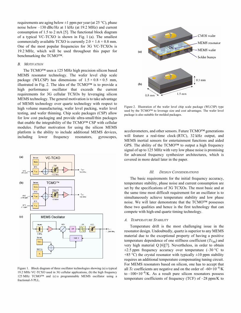
The TCMO™ uses a 125 MHz high precision silicon basedMEMS resonator technology. The wafer level chip scalepackage (WLCSP) has dimensions of 1.5 × 0.8 × 0.5 mm,illustrated in Fig. 2. The idea of the TCMO™ is to provide ahigh performance oscillator that exceeds the currentrequirements for 3G cellular TCXOs by leveraging siliconMEMS technology. The general motivation is to take advantageof MEMS technology over quartz technology with respect tohigh volume manufacturing, wafer level packing, wafer leveltesting, and wafer thinning. Chip scale packages (CSP) allowfor low cost packaging and provide ultra-small/thin packagesthat enable the integrability of the TCMO™ CSP with cellularmodules. Further motivation for using the silicon MEMSplatform is the ability to include additional MEMS devices,including lower frequency resonators, gyroscopes,
accelerometers, and other sensors. Future TCMO™ generationswill feature a real-time clock (RTC), 32 kHz output, andMEMS inertial sensors for entertainment functions and aidedGPS. The ability of the TCMO™ to output a high frequencysignal of up to 125 MHz with very low phase noise is promisingfor advanced frequency synthesizer architectures, which iscovered in more detail later in the paper.
III. DESIGN CONSIDERATIONS
The basic requirements for the initial frequency accuracy,temperature stability, phase noise and current consumption areset by the specifications of 3G TCXOs. The most basic and atthe same time most difficult requirement for an oscillator is tosimultaneously achieve temperature stability and low phasenoise. We will later demonstrate that the TCMO™ possessesthese two qualities and hence is the first technology that cancompete with high-end quartz timing technology.
A. TEMPERATURE STABILITY
Temperature drift is the most challenging issue in theresonator design. Undoubtedly, quartz is superior to any MEMSmaterial due to the exceptional property of having a positivetemperature dependence of one stiffness coefficient (Tc66) andvery high material Q [6][7]. Nevertheless, in order to obtain±2.5 ppm frequency accuracy over temperature (–30 °C to+85 °C) the crystal resonator with typically ±10 ppm stabilityrequires an additional temperature compensating tuning circuit.For MEMS resonators based on silicon, one has to accept thatall Tc coefficients are negative and on the order of –60×10–6/Kto –100×10–6/K. As a result pure silicon resonators possesstemperature coefficients of frequency (TCF) of –28 ppm/K to
Figure 1. Block diagram of three oscillator technologies showing (a) a typical19.2 MHz VC-TCXO used in 3G cellular applications, (b) the high frequency125 MHz TCMO™ and (c) a programmable MEMS oscillator using afractional-N PLL.
(a)
(b)
(c)
Figure 2. Illustration of the wafer level chip scale package (WLCSP) typeused by the TCMO™ to leverage size and cost advantages. The wafer levelpackage is also suitable for molded packages.
(a)
(b)

–31 ppm/K [8]. In order to obtain a temperature drift of±2.5 ppm the oscillator would require a tuning range of around3,500 ppm. In general, any tuning of the resonator or theoscillator will affect the equivalent circuit of the resonator or itsperformance in the oscillator loop. Hence, the phase noise willdeteriorate. In addition, the large second order stiffnessdependence of silicon causes a nonlinear deviation of the TCFof around 90 ppm over a –30 °C to +85 °C temperature rangeand it has to be accounted for in order to obtain ±2.5 ppmstability. Tuning of the oscillator loop is avoided in case ofusing a fractional-N phase locked loop (PLL) to adjust theuncompensated reference frequency from the MEMS oscillatorloop according to the temperature, as shown in Fig. 1 (c). Twocommercial MEMS oscillator companies, Discera and SiTimeuse this approach and use the fractional-N PLL at the same timeto generate any frequency from 1 MHz to200 MHz [9][10][11]. The disadvantage of the digitalcompensation is the elevated phase noise and discontinuities infrequency and phase, rendering both solutions unsuitable forcellular applications [2][11][12].
The necessity to use analog tuning requires the tuning tooccur in the oscillator loop, as done for TCXOs. Furthermore,the tuning range has to exceed the temperature drift. Possiblemethods of controlling the temperature drift of a MEMSresonator include compensating heating [13][14], temperaturedependent electrostatic biasing [15], electrostatic stiffnesscontrol [16], switching of resonator arrays [17], dynamic massloading [18] and composite structures [19][20]. A suitablechoice for 3G cellular oscillators should be made keeping inmind the manufacturability, current consumption, phase noise,voltage limits, frequency continuity, and aging. In most cases,except for an ovenized solution as an OCXO, unwanted modesmay cause activity dips for certain temperatures and as a resultcause unexpected frequency shifts [21]. The origin for activitydips lies in unwanted modes with large TCF and closeproximity to the main mode interfering with the oscillation onthe main mode. As a result, the design and control of spuriousmodes in the vicinity of the resonance frequency within theprocess margins are important, which can significantly lowerthe cost of testing, as it enables the use of a larger temperatureresolution.
Some applications such as GPS require consideration of thetemperature slew rate, i.e. the frequency change due to atemperature transient. For example, it is challenging for a GPSreceiver to obtain a first fix if the frequency slew rate is largerthan 0.1 ppm/s. The proximity and good thermal coupling ofresonator and circuit are the key to reduce the temperature slewrate in oscillators. Although the TCF of AT-cut quartzresonators is mostly 3 to 5 times smaller than for first ordercompensated silicon resonators, the thermal conductivity ofquartz is inferior to silicon. The WLCSP of the TCMO™ shownin Fig. 2 features ultimate proximity of IC and resonator andexcellent thermal coupling. Therefore, the TCMO™ ispromising for the reduction of the temperature slew rate beyondthe capabilities of quartz.
B. PHASE NOISE
Having chosen a resonator technology that offers a tuningrange exceeding the temperature drift, we are ready to examinethe phase noise. Analog tuning will always affect the phasenoise performance. A 3G VC-TCXO requires a tunability of±25 ppm alone for the temperature drift compensation and forthe electrical frequency control (EFC) tuning, neglecting thetuning required to adjust for the residual initial frequencyaccuracy after manufacturing and trimming. However, high Qcrystal resonators resist such large de-tuning off resonance. Asa result, the crystal resonator is de-Q’d with the oscillatorcircuit, resulting in lowered loaded Q and elevated phase noise.The inherent advantage of crystal oscillators lies in the use ofthe temperature stable AT-cut, so that the trade-off of tunabilityfor temperature stability and phase noise deterioration areminimal.
The phase noise is also affected by other tuning mechanismsmentioned above, either because the tuning mechanism directlyaffects the resonator Q and motional resistance of the resonator,or the resonator is operated off resonance, or less power isavailable to the resonator or simply because noise is injected onthe tuning signal itself, or any combination of the above.Additional considerations for low phase noise are the resonatorQ, power available to the resonator in the oscillator loop,maximum current of 1-1.5 mA for the oscillator in order tomake the 3G TCXO spec, circuit flicker noise, materials,nonlinearity of the resonator, vibration isolation, processingtechniques and packaging.
Typical phase noise specifications for a 19.2 MHz oscillatorfor 3G would be –110 dBc/Hz at 100 Hz, –130 dBc/Hz at1 kHz, –140 dBc/Hz at 10 kHz, –145 dBc/Hz at 100 kHz offset.Commercial MEMS oscillator solutions use a silicon resonatorwith a natural frequency of 5.1 MHz having phase noise of–115 dBc/Hz at 10 kHz [22] and a polysilicon beam thatvibrates at 19.2 MHz and achieves –106 dBc/Hz at 1 kHzoffset [23]. Relating these values to the typical 3G phase noiserequirements at 19.2 MHz shows that both technologies violatethe specifications by 24 dBc/Hz at 1 kHz and 36 dBc/Hz at10 kHz, respectively. It is obvious that it is very challenging forany MEMS oscillator technology to achieve low phase noiseand low temperature drift, including tuning, and that thetechnological approach in the design phase determines whetherthis is possible at all.
C. TCMO™ TECHNOLOGY PLATFORM
The TCMO™ uses a silicon-based MEMS resonator that issuspended and acoustically decoupled from the silicon substrateusing a special engineered substrate. The process flow of theTCMO™ is illustrated in Fig. 3. The fabrication begins with theformation of an engineered substrate, i.e. an SOI wafer with apredefined cavity hidden in the handle silicon layer. In thesecond step, through-silicon vias (TSV) are formed in theengineered substrate. In the third step, the backside routing isprepared for final solder bumping. In the fourth step, the MEMSresonator is formed by using DRIE to etch through the device

silicon layer and to release the resonator structure. The buriedcavity has the great advantage that the release of the resonatorusing dry etching is very fast and clean. The lack of a sacrificiallayer and wet etching chemistry prevent any stiction effects anda time consuming removal of the sacrificial material. In the fifthstep, the CMOS IC wafer and the MEMS wafer are bondedtogether creating the interconnects and hermetic seal around theMEMS resonator. In the final step, the wafer undergoes thedeposition of underbump metallization (UBM) and solderbumps.
D. WAFER LEVEL CHIP SCALE (WLCSP) PACKAGE
The TCMO™ uses a wafer bonding process of the CMOSwafer and MEMS wafer to create a hermetic CSP. During thebonding process, electrical and thermal interconnects betweenboth wafers are made. None of the TSVs are connected to theMEMS resonator. Instead, they are directly routed through tothe IC. The TCMO™ will be available as WLCSP with a formfactor of 1.5 × 0.8 × 0.5 mm, as illustrated in Fig. 2. A plasticsurface mount dual flat no-lead (DFN) package compatible withfootprints for 2520 and 2016 TCXOs will also be offered.
IV. THE PROTOTYPE β-TCMO™A beta prototype of the TCMO™ with the silicon MEMS
resonator has been developed on a printed circuit board (PCB)with the use of off-the-shelf circuit components. For theβ-TCMO™, the MEMS resonator was fabricated according tothe process flow in Fig. 3, omitting steps 5 and 6. Instead of theWLCSP the MEMS resonator was packaged in a standard6.2 × 4.3 mm LCC ceramic package. This package iscommonly used for crystals, and it ensures a hermetic seal of theMEMS resonator and ease of handling during test andassembly. The MEMS resonator assembled on the β-TCMO™prototype board is shown in Fig. 4.
A. PHASE NOISE MEASUREMENTS
The phase noise of the beta MEMS oscillator is shown inFig. 5. The single sideband (SSB) phase noise of the betageneration of the TCMO™ is measured with an AgilentE5052B signal source analyzer. In this case, the oscillatoroutput frequency is set by the natural resonance frequency of123.9 MHz of the MEMS resonator and the initial applied
Figure 3. Process flow of the TCMO™ fabrication process. The key featuresinclude the engineered substrate, through-silicon vias (TSV) and the waferbonding process to obtain a wafer level chip scale package (WLCSP).
Figure 4. Image of the beta version of the TCMO™ prototype board that isbeing transferred to a fully integrated solution. (a) The backside of the circuitboard comprises the MEMS resonator in a LCC ceramic package and atemperature sensor beside it. The synthesizer and temperature control areimplemented on the frontside (b).
Figure 5. Measured single sideband phase noise of the 123.9 MHztemperature compensated MEMS oscillator (TCMO™) and phase noiseconverted to a 19.2 MHz carrier.

tuning voltage of 4.5 V. The MEMS oscillator achieves a phasenoise of –91 dBc/Hz at 100 Hz, –120 dBc/Hz at 1 kHz,–146 dBc/Hz at 10 kHz and –152 dBc/Hz at 100 kHz offsetfrom the 123.9 MHz carrier and a noise floor of –150 dBc/Hzfor offsets beyond 100 kHz. Converting the phase noise fromthe 123.9 MHz carrier to a 19.2 MHz carrier, using theapproximation that the phase noise decreases for the dividerfactor N as –20 Log(N), yields the second trace in Fig. 5. In caseof the conversion in an IC, the noise floor will be limited toaround –165 dBc/Hz to –155 dBc/Hz depending on thetechnology.
B. OSCILLATOR TUNING
The technological key that enables us to achieve an accurateinitial frequency of the oscillator and correct for temperatureexcursions during operation is based on novel tuning andcompensation circuit architectures, developed and patented bySand 9. As mentioned earlier, tuning of the oscillator frequencywill always be associated with a degradation of the phase noise.Therefore, a significant design challenge is to minimize therequired tuning range in combination with a tuning circuit thatcauses minimum deterioration of the phase noise. In our case,the coherent choice of the oscillator architecture and the MEMSresonator, combined with a precise integrated design minimizesthe degradation over the required tuning range. The phase noisefor different tuning voltages is shown in Fig. 6.
The phase noise characteristics of the TCMO™ are almostunaffected by the tuning. Figure 7 shows the tuningcharacteristics of the carrier frequency of the oscillator versusthe applied tuning voltage along with the phase noise value at1 kHz. For very large tuning voltages, the phase noise doesdegrade rapidly, and at 6.7 V, the oscillator becomes unstableand starts to oscillate at a different frequency. The ±200 ppm
range indicated in Fig. 7 represents the feasible tuning rangethat does not cause strong degradation of the phase noise of theoscillator or adversely affect the stability. The correspondingvoltage range is from 0.6 V to about 6.1 V.
The worst-case phase noise at 1 kHz is therefore–116 dBc/Hz, corresponding to a worst-case degradation of4.6 dBc/Hz beyond the phase noise at 1 kHz for the ideal tuningvoltage of 4.5 V. The worst-case phase noise at 100 Hz offset is–88 dBc/Hz, at 10 kHz offset it is –140 dBc/Hz and at 100 kHzoffset it is –151 dBc/Hz. Converting this to a 19.2 MHz carriercorresponds to –104 dBc/Hz at 100 Hz, –132.5 dBc/Hz at1 kHz and –156.3 dBc/Hz at 10 kHz. Based on the 3Gspecifications and the uncertainty of the phase noisemeasurement the TCMO™ does not achieve the phase noisespecifications at 100 Hz offset for the current β-generation.However, we will see later in the section on novel timingarchitectures that a direct 125 MHz reference frequencycompared to a 19.2 MHz reference leads to a phase noisereduction in the cellular frequency synthesizer of about 8 dB.As a result, the 125 MHz TCMO™ would meet the 3G phasenoise requirements.
Figure 6. Tuning voltage dependence of the single sideband phase noise ofthe 123.9 MHz temperature compensated MEMS oscillator.
Figure 7. Result of the frequency tuning of the MEMS oscillator anddependence of the 1 kHz phase noise versus the tuning voltage from 0 to 7 Vmeasured with an Agilent E5052B signal source analyzer.
C. TEMPERATURE STABILITY
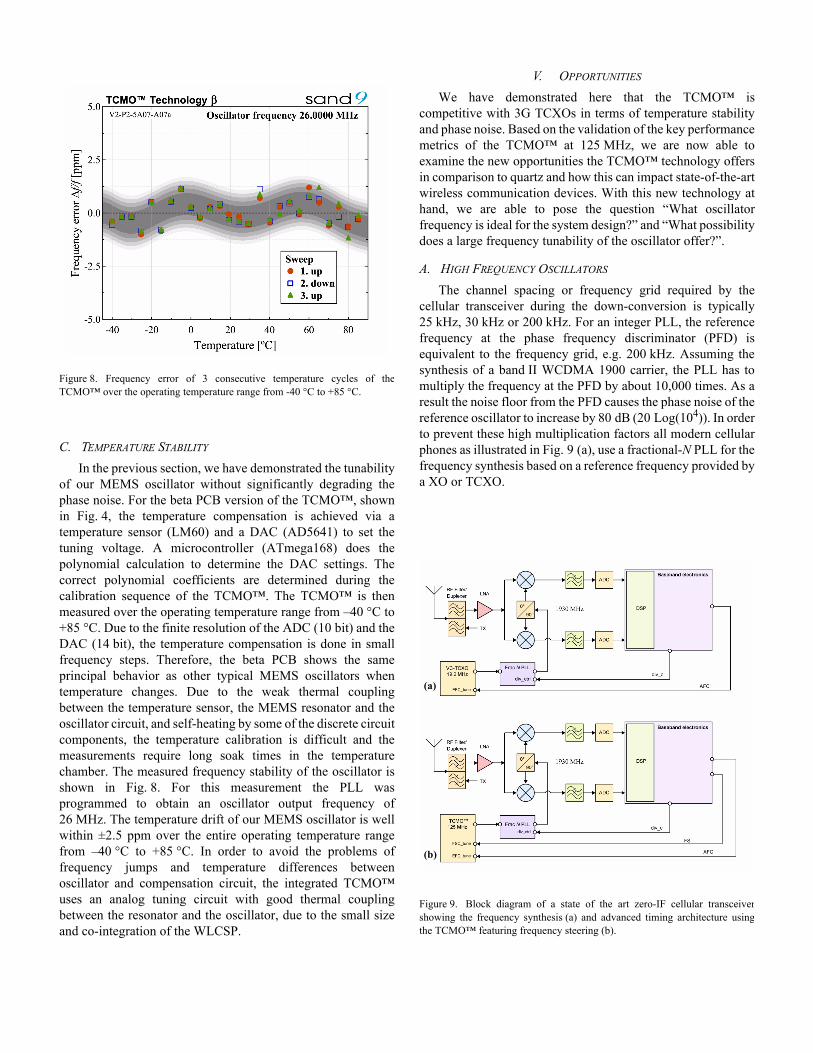
In the previous section, we have demonstrated the tunabilityof our MEMS oscillator without significantly degrading thephase noise. For the beta PCB version of the TCMO™, shownin Fig. 4, the temperature compensation is achieved via atemperature sensor (LM60) and a DAC (AD5641) to set thetuning voltage. A microcontroller (ATmega168) does thepolynomial calculation to determine the DAC settings. Thecorrect polynomial coefficients are determined during thecalibration sequence of the TCMO™. The TCMO™ is thenmeasured over the operating temperature range from –40 °C to+85 °C. Due to the finite resolution of the ADC (10 bit) and theDAC (14 bit), the temperature compensation is done in smallfrequency steps. Therefore, the beta PCB shows the sameprincipal behavior as other typical MEMS oscillators whentemperature changes. Due to the weak thermal couplingbetween the temperature sensor, the MEMS resonator and theoscillator circuit, and self-heating by some of the discrete circuitcomponents, the temperature calibration is difficult and themeasurements require long soak times in the temperaturechamber. The measured frequency stability of the oscillator isshown in Fig. 8. For this measurement the PLL wasprogrammed to obtain an oscillator output frequency of26 MHz. The temperature drift of our MEMS oscillator is wellwithin ±2.5 ppm over the entire operating temperature rangefrom –40 °C to +85 °C. In order to avoid the problems offrequency jumps and temperature differences betweenoscillator and compensation circuit, the integrated TCMO™uses an analog tuning circuit with good thermal couplingbetween the resonator and the oscillator, due to the small sizeand co-integration of the WLCSP.
V. OPPORTUNITIES
We have demonstrated here that the TCMO™ iscompetitive with 3G TCXOs in terms of temperature stabilityand phase noise. Based on the validation of the key performancemetrics of the TCMO™ at 125 MHz, we are now able toexamine the new opportunities the TCMO™ technology offersin comparison to quartz and how this can impact state-of-the-artwireless communication devices. With this new technology athand, we are able to pose the question “What oscillatorfrequency is ideal for the system design?” and “What possibilitydoes a large frequency tunability of the oscillator offer?”.
A. HIGH FREQUENCY OSCILLATORS
The channel spacing or frequency grid required by thecellular transceiver during the down-conversion is typically25 kHz, 30 kHz or 200 kHz. For an integer PLL, the referencefrequency at the phase frequency discriminator (PFD) isequivalent to the frequency grid, e.g. 200 kHz. Assuming thesynthesis of a band II WCDMA 1900 carrier, the PLL has tomultiply the frequency at the PFD by about 10,000 times. As aresult the noise floor from the PFD causes the phase noise of thereference oscillator to increase by 80 dB (20 Log(104)). In orderto prevent these high multiplication factors all modern cellularphones as illustrated in Fig. 9 (a), use a fractional-N PLL for thefrequency synthesis based on a reference frequency provided bya XO or TCXO.
Figure 8. Frequency error of 3 consecutive temperature cycles of theTCMO™ over the operating temperature range from -40 °C to +85 °C.
Figure 9. Block diagram of a state of the art zero-IF cellular transceivershowing the frequency synthesis (a) and advanced timing architecture usingthe TCMO™ featuring frequency steering (b).
(a)
(b)

The synthesized frequency fout is given as:
, (1)
where fPFD is the reference frequency at the PFD, N is theinteger multiplier, F the fractional channel of operation, and Mthe fractional modulus. The fractional relation of fout and fPFDimplies that a much higher reference frequency at the PFD canbe used resulting in smaller multiplication factors. The expectedimprovement in the phase noise of 20 Log(N) is reduced due tothe fact that the PFD adds more noise at higher frequencies. Aphase noise improvement of 10 Log(N) is realistic. Assumingthe synthesis of a carrier frequency of 1990 MHz using a19.2 MHz TCXO as reference at the PFD requires N = 103,M = 96 and F = 62. Compared to the integer PLL, the resultingphase noise is lowered by 20 dB. This result would suggest that,in order to reduce the phase noise of the frequency synthesizer,the reference frequency at the PFD should be as high aspossible. In practice, driving the PFD for standard CMOStechnology beyond a frequency of 130 to 150 MHz will causestrong degradation of the phase noise. Use of a 125 MHzTCMO™ instead of a 19.2 MHz TCXO as reference at the PFDyields an improvement of approximately 8 dB in phase noise.Therefore, the phase noise of the 125 MHz TCMO™ shownearlier exceeds the performance of 3G TCXOs.
B. INTERFERENCE AVOIDANCE
The increased number of bands, complexity and integrationdensity of RF front-ends in cellular devices have made thedesign more challenging. The number of interferences andspecification violations require multiple re-spins of the designto obtain a production-ready part. One of the difficulties is theavoidance of birdies, or interferences that affect acommunication channel and render it useless. This willgenerally require a redesign. The origin of birdies is manifold.Most birdies are the result of unwanted mixing products ofspurs or leakage of the PLL and higher harmonics of thereceived signal. For a given PLL setting these mixing productsinterfere with the selected channel and obscure the actual signal.We have seen earlier that the TCMO™ features a ±200 ppmtuning range, as shown in Fig. 7. For band II WCDMA, with thelow frequency edge of 1930 MHz and channel spacing of200 kHz, the maximum relative channel spacing is 104 ppm.Assuming that only ±75 ppm of the TCMO™ tuning arerequired for the temperature compensation and ±15 ppm areused for the EFC tuning identical to VC-TCXOs, it leaves uswith ±105 ppm of tuning that can be used for electricalfrequency steering (EFS). The TCMO™ having both an EFCand EFS port is shown in Fig. 1 (b). The block diagram of acellular transceiver using a TCMO™ with frequency steering isshown in Fig. 9 (b). The motivation for the frequency steeringis that for a given channel frequency three different PLLsettings exist, so that a birdie can be avoided by using one of theother two possibilities. As an example, for the 125 MHz
TCMO™ to generate a carrier frequency of 1930 MHz, thefractional-N PLL settings become N = 15, M = 625 andF = 275. However, for the case of pulling the TCMO™ by–103.62 ppm and using F = 276, we can generate the same1930 MHz carrier. Another possibility is to de-tune theTCMO™ by +103.64 ppm and use F = 274 to obtain a1930 MHz carrier. The frequency steering option is aprogrammable feature of the TCMO™ and should not beconfused with the analog AFC tuning of typically ±15 ppm. Useof an external analog voltage for the frequency steeringdegrades the phase noise performance due to the required largetuning sensitivity. In order for a 3G VC-TCXO to offer thislarge tunability, the loaded Q of the crystal resonator wouldhave to be considerably lowered by the oscillator circuit. As aresult the phase noise would deteriorate and violate the requiredspecifications.
VI. DISCUSSION
We have demonstrated that the TCMO™ is able to achievethe combination of temperature stability and low phase noiseusing an analog tuning technique. To the best of our knowledge,here, for the first time, a MEMS oscillator has achieved thiscombination. The performance of six β-TCMO™ prototypeboards has been validated by major semiconductor companiesand government laboratories. The concept of the TCMO™technology has been enthusiastically embraced by majorwireless IC and handset manufacturers. With the 125 MHzWLCSP TCMO™ we are looking forward to demonstrateminiature size, low current consumption, low aging andmanufacturability in high volume, in addition to temperaturestability and low phase noise.
VII. CONCLUSION
We believe Sand 9 is the first group to demonstrate a MEMSoscillator technology that can compete with VC-TCXOs used in3G cellular applications in terms of temperature stability andphase noise. The temperature drift of the temperaturecompensated MEMS oscillator (TCMO™) is within ±2.5 ppmover the entire operating temperature range from –40 °C to+85 °C. The TCMO™ achieves a worst-case phase noise of–116 dBc/Hz at 1 kHz offset from the 123.9 MHz carrier,relating to a worst case phase noise value of –132.5 dBc/Hz at1 kHz offset at 19.2 MHz. Using our high frequency 125 MHzTCMO™ as reference oscillator for 3G cellular applicationsimproves the phase noise significantly. The large tunability ofthe TCMO™ enables frequency steering and allows for birdieavoidance. The TCMO™ uses an analog temperaturecompensation technique similar to a TCXO, and therefore, doesnot experience the deterioration of phase noise and jitter norexhibit sudden jumps in phase, that plague commerciallyavailable fractional-N PLL based MEMS oscillators. In future,the goal is to build on the TCMO™ technology to include a realtime clock and MEMS inertial sensors.
fout fPFD N FM-----+⎝ ⎠
⎛ ⎞=

REFERENCES
[1] M. S. McCorquodale, “Self-Referenced, Trimmed andCompensated RF CMOS Harmonic Oscillators asMonolithic Frequency Generators”, IEEE Freq. Contr.Symp. 2008, pp. 408-413.
[2] C.S. Lam, “A Review of the Recent Development ofMEMS and Crystal Oscillators and Their Impacts on theFrequency Control Products Industry”, Proceedings of theIEEE Int. Ultrason. Symp. 2008, pp. 694-704.
[3] B. Neubig, “MEMS-Oscillators- Opportunities andLimitations (German)”, Markt & Technik, 37, pp. 28-29,(http://www.axtal.com/info/MuT_37_08.pdf), 2008.
[4] K. J. Schoepf, R. Rebel, D. M. Chen, G. Zolfagharkhani,A. Gaidarzhy, J. H. Kuypers, M. Crowley, P. Mohanty,“TCMO™: A Versatile MEMS Oscillator TimingPlatform”, Proc. PTTI 2009, in press.
[5] http://www.kds.info/data/pdf/056E.pdf.[6] R. Bechmann, A. D. Ballato, T. J. Lukaszek, “Higher Order
Temperature Coefficients of the Elastic Stiffness andCompliances of Alpha-quartz”, Techn. Rep. 2261, USArmy, Fort Monmouth, New Jersey, 1963, p. 25.
[7] J. F. Rosenbaum, “Bulk Acoustic Wave Theory andDevices”, Artech House Inc., 1988, ISBN 0-89006-265-X.
[8] C. Bourgeois, E. Steinstand, N. Blanc, N.F. de Rooij,“Design of Resonators for the Determination of theTemperature Coefficients of Elastic Constants ofMonocrystalline Silicon”, IEEE Freq. Contr. Symp. 1997,pp. 791-799.
[9] http://www.discera.com[10]http://www.sitime.com[11]W.-T. Hsu, “Recent Progress in Silicon MEMS
Oscillators”, Proc. PTTI Meeting 2008, pp. 135-146.
[12]R. Henry, D. Kenny, “Comparative Analysis of MEMS,Programmable, and Synthesized Frequency ControlDevices Versus Traditional Quartz Based Devices”, IEEEFreq. Contr. Symp. 2008, pp. 396-401.
[13]R. C. Ruby, P. P. Merchant, “Method of Making TunableThin Film Acoustic Resonators”,US5873153.
[14]M. Lutz, A. Partridge, “Temperature Controlled MEMSResonator and Method for Controlling ResonatorFrequency”, US7427905.
[15]M. Lutz, A. Partridge, “Temperature Compensation forSilicon MEMS Resonator”, US6987432.
[16]C. C. T. Nguyen, W.-T. Hsu, “Mechanical ResonatorDevice Having Phenomena-Dependent ElectricalStiffness”, US6958566.
[17]E. P. Quevy, R. T. Howe, “Temperature CompensatedOscillator Including MEMS Resonator for FrequencyControl”, US7211926.
[18]D. H. Bernstein, R. T. Howe, E. P. Quevy, “MEMSStructure Having a Compensated ResonatingMember”,US7591201.
[19]M. Lutz, A. Partridge, “Temperature Compensation forSilicon MEMS Resonator”, US7202761.
[20] J. D. Larson III, J. Choy, John, D. E. Lee, K. J. Grannen, H.Feng, C. A. Rogers, U. C. Sridharan, “Film Bulk AcousticResonator (FBAR) Devices with TemperatureCompensation”, US7561009
[21]A. F. B. Wood, A. Seed, “Activity Dips in AT-CutCrystals”, Proc. Ann. Freq. Contr. Symp. 1967,pp. 420-435.
[22]http://www.sitime.com/news/releases/sit0100102306.htm.[23]http://www.mwrf.com/Article/ArticleID/5767/5767.html.