Embed Size (px)
Citation preview

High Performance Embedded Computing Workshop at MIT/LL (23-25 September 2003)
1. Title: Hybrid Optical/Digital Processor for Radar Imaging 2. Authors:
Mr. Keith Frampton Essex Corporation 9150 Guilford Road Columbia, MD 21046 301-953-7875 301-953-7880 (fax) [email protected] US Citizen Mr. Patrick Stover Annapolis Micro Systems, Inc. 190 Admiral Cochrane Dr. Suite 130 Annapolis, MD 21401 410-841-2514 410-841-2518 (fax) [email protected] US Citizen
3. Author notation: First: Mr. Keith Frampton Corresponding: Mr. Patrick Stover Presenting: Mr. Keith Frampton 4. Presentation session: Presentation does not need to be limited to the US Only session. 5. Presentation format: Authors prefer an oral presentation. 6. Areas of work addressed: a. Embedded Computing for Global Sensors and Information Dominance b. Advanced Digital Front-End Processors c. Automated Tools for Embedded System Development

Report Documentation Page Form ApprovedOMB No. 0704-0188
Public reporting burden for the collection of information is estimated to average 1 hour per response, including the time for reviewing instructions, searching existing data sources, gathering andmaintaining the data needed, and completing and reviewing the collection of information. Send comments regarding this burden estimate or any other aspect of this collection of information,including suggestions for reducing this burden, to Washington Headquarters Services, Directorate for Information Operations and Reports, 1215 Jefferson Davis Highway, Suite 1204, ArlingtonVA 22202-4302. Respondents should be aware that notwithstanding any other provision of law, no person shall be subject to a penalty for failing to comply with a collection of information if itdoes not display a currently valid OMB control number.
1. REPORT DATE 23 SEP 2003
2. REPORT TYPE N/A
3. DATES COVERED -
4. TITLE AND SUBTITLE Hybrid Optical/Digital Processor for Radar Imaging
5a. CONTRACT NUMBER
5b. GRANT NUMBER
5c. PROGRAM ELEMENT NUMBER
6. AUTHOR(S) 5d. PROJECT NUMBER
5e. TASK NUMBER
5f. WORK UNIT NUMBER
7. PERFORMING ORGANIZATION NAME(S) AND ADDRESS(ES) Essex Corporation 9150 Guilford Road Columbia, MD 21046; AnnapolisMicro Systems, Inc. 190 Admiral Cochrane Dr. Suite 130 Annapolis, MD 21401
8. PERFORMING ORGANIZATIONREPORT NUMBER
9. SPONSORING/MONITORING AGENCY NAME(S) AND ADDRESS(ES) 10. SPONSOR/MONITOR’S ACRONYM(S)
11. SPONSOR/MONITOR’S REPORT NUMBER(S)
12. DISTRIBUTION/AVAILABILITY STATEMENT Approved for public release, distribution unlimited
13. SUPPLEMENTARY NOTES See also ADM001694, HPEC-6-Vol 1 ESC-TR-2003-081; High Performance Embedded Computing(HPEC) Workshop(7th). , The original document contains color images.
14. ABSTRACT
15. SUBJECT TERMS
16. SECURITY CLASSIFICATION OF: 17. LIMITATION OF ABSTRACT
UU
18. NUMBEROF PAGES
36
19a. NAME OFRESPONSIBLE PERSON
a. REPORT unclassified
b. ABSTRACT unclassified
c. THIS PAGE unclassified
Standard Form 298 (Rev. 8-98) Prescribed by ANSI Std Z39-18
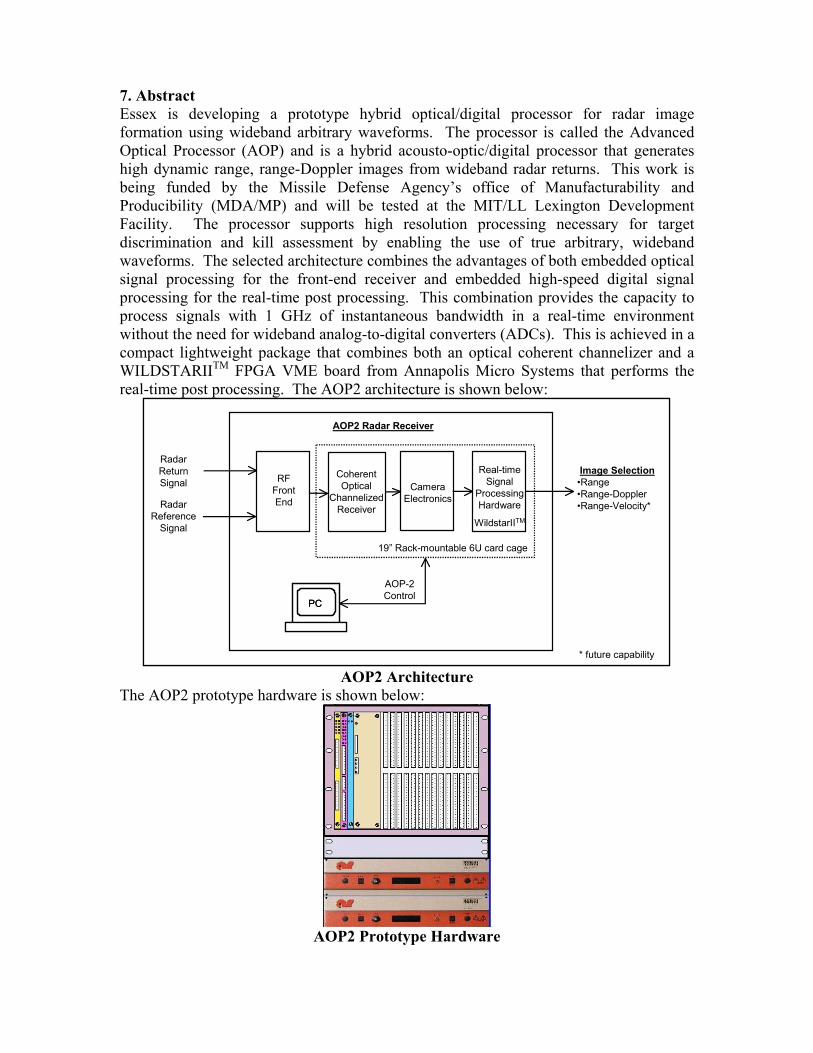
7. Abstract Essex is developing a prototype hybrid optical/digital processor for radar image formation using wideband arbitrary waveforms. The processor is called the Advanced Optical Processor (AOP) and is a hybrid acousto-optic/digital processor that generates high dynamic range, range-Doppler images from wideband radar returns. This work is being funded by the Missile Defense Agency’s office of Manufacturability and Producibility (MDA/MP) and will be tested at the MIT/LL Lexington Development Facility. The processor supports high resolution processing necessary for target discrimination and kill assessment by enabling the use of true arbitrary, wideband waveforms. The selected architecture combines the advantages of both embedded optical signal processing for the front-end receiver and embedded high-speed digital signal processing for the real-time post processing. This combination provides the capacity to process signals with 1 GHz of instantaneous bandwidth in a real-time environment without the need for wideband analog-to-digital converters (ADCs). This is achieved in a compact lightweight package that combines both an optical coherent channelizer and a WILDSTARIITM FPGA VME board from Annapolis Micro Systems that performs the real-time post processing. The AOP2 architecture is shown below:
RFFrontEnd
Camera Electronics
Real-time Signal
ProcessingHardware
WildstarIITM
Radar Reference
Signal
Radar ReturnSignal
19” Rack-mountable 6U card cage
AOP-2 Control
PC
AOP2 Radar Receiver
Image Selection•Range•Range-Doppler•Range-Velocity*
* future capability
Coherent Optical
ChannelizedReceiver
RFFrontEnd
Camera Electronics
Real-time Signal
ProcessingHardware
WildstarIITM
Radar Reference
Signal
Radar ReturnSignal
19” Rack-mountable 6U card cage
AOP-2 Control
PCPC
AOP2 Radar Receiver
Image Selection•Range•Range-Doppler•Range-Velocity*
* future capability
Coherent Optical
ChannelizedReceiver
AOP2 Architecture
The AOP2 prototype hardware is shown below:
AOP2 Prototype Hardware

The production hardware can easily fit into a single 6U card cage, as shown below, without significant development costs.
OpticalReceiver RFFE Amps
Waveform generators
Amplifiers
RF front-end & LOs
Optical receiver
Camera & timing
Processing & control card
Controller
OpticalReceiver RFFE Amps
Waveform generators
Amplifiers
RF front-end & LOs
Optical receiver
Camera & timing
Processing & control card
Controller AOP Production Configuration
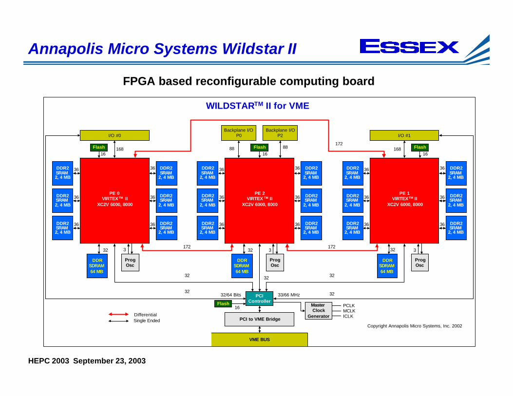
By removing complex software and custom digital hardware, the cost for this processor is significantly less than an “all-digital” solution, even in modest quantities. The cost effectiveness of this processor allows use at the sub-array level for desired operational flexibility and performance enhancements, such as beamforming and STAP. The development of this processor has been accelerated with the use of the AMS CoreFireTM FPGA Application Builder. This tool has allowed the mapping of the post processing algorithms to the COTS AMS FPGA hardware with minimal effort. Selected AOP2 algorithms were running as a demonstration in the WildstarIITM for the AOP2 critical design review with just a few weeks of effort. CoreFire™ also provided a hardware-in-the-loop debugger that allowed us to insert test data into the designs in the FPGAs and then review the test vectors from the host as they ran through each part of the algorithm. The AMS hardware configuration is a 6U form factor with 3 Xilinx Virtex IITM 6000 series FPGAs. This WILDSTARII board also has two I/O daughter card positions providing in excess of 4 GB/s I/O bandwidth. The DSP algorithms running in this hardware include:
1. data formatting algorithms 2. calibration algorithms 3. range-compression algorithm 4. Doppler compression algorithm 5. data storage formatting 6. display formatting 7. system timing and control functions
The chosen hardware can perform these algorithms in real-time and is flexible such that changes in the algorithms are easily accommodated. There is no operating system required so integration issues with a single board VME control computer are minimal. Presented in this paper will be the architecture description and integration of the optical and FPGA technologies, along with updated test results.

Hybrid Optical/Digital Processor for Radar Imaging
Keith FramptonEssex Corporation9150 Guilford Road
Columbia, MD 21046301-953-7875
Pat StoverAnnapolis Micro Systems
190 Admiral Cochrane Dr. Suite 130Annapolis, MD 21401
23 September 2003

HEPC 2003 September 23, 20032
Problem Statement and Solution
• Problem:– Projected BMD threat environment will have clutter and EMI– LFM waveforms have limitations with these threats– Desired advanced waveforms (chaotic, PRN*, …) are very
processing intensive
• Solution:– The advanced optical processor (AOP) generates
range-Doppler images from advanced arbitrary waveforms– AOP architecture incorporates:
•Embedded optical signal processing•Embedded digital signal processing in FPGAs

HEPC 2003 September 23, 20033
Program Objectives
• Modernize the architecture, scaling to:– 1 GHz– Real-time operation – Full complex, single pass– Store images in real-time to disk
• Compact rack stackable configuration
6U Card Cage
Power Supplies

HEPC 2003 September 23, 20034
AOP 2 Performance Characteristics
0.15 metersRange Resolution
100 usec minimum10 kHz maximum
Pulse Repetition Interval (PRI)Pulse Repetition Frequency (PRF)
+/- 5 degreesPhase Deviation from Linear in CPS
+/- 0.1 dBRCS Repeatability
3 dB uncorrected; 1 dB correctedFrequency Response
-34 dBRange Sidelobes (Hamming weighting)
153 meters (+/-76.7 m about image center)Range Extent
1024 bins (+/- 512 about image center)Range Bins
6 dB maximum @ +/- 76.7 meters relative to image center
SNR Loss vs. Range center
85 dB for 128 coherently integrated pulsesSpur Free Dynamic Range
66 dBPost-Compression Dynamic Range (peak to RMS noise)
10 MHzStable Reference Frequency
1 GHzBandwidth (-3dB)
Tunable 5 GHz to 7 GHz (TBR)Center Frequency
10 ? sec to 50 msecPulse Width

HEPC 2003 September 23, 20035
Algorithm Functionality is Similar
OPT_97.CVS
optical domain digital domain
A/DSum
OpticalFT
OpticalFT
X
Equalization,weighting,compensation, &non-linear ops.
X IFFT FFT
Compressedin range
Compressedin Doppler
Range-DopplerMap
RadarReturn
RadarReference
Optical/Digit al Implementa tion
Dig_96.CVS
A/D Presum FFT
FFT
XEqualization
X IFFT FFT
Compressedin range
Compressedin Doppler
Range-DopplerMap
RadarReturn
RadarReference
Digital Implement ation

HEPC 2003 September 23, 20036
PROCFLW2.CVS
Dop
pler
, ?
Radar Bandwidth(Frequency, f )
Tim
e, t
(1-D FFTs)
Acousto-Opt icUn it
Retur n
Referenc e
Digital SignalProcessing Un it
(2D FFT)
ComplexR ange
D opplerD ata
pu lsecompression
Range, ?
(1-D FF Ts)
S = spectrum of radar return signalR = spectrum of radar reference signal
STCS(f,t) PP(t,?)
CAF(??? )
Tim
e,
t
Range, ?
Process Flow
Cross power spectra vs. time
Correlator compresses pulse in range
FFT compresses pulses in Doppler
Frequency of each fringe is proportional to range.
Phase change over time is proportional to Doppler.

HEPC 2003 September 23, 20037
AOP2 Functional Configuration
RFFrontEnd
Optics Camera Electronics
Real-time Signal
ProcessingHardwareRadar
Reference Signal
Radar ReturnSignal
19” Rack-mountable 6U card cage
AOP-2 Control
PC
AOP2 Radar Receiver
Image Selection•Range•Range-Doppler•Range-Velocity*
* future capability

HEPC 2003 September 23, 20038
AOP 2 Top Level System Diagram
Controller
VME64
Ethernet
Signal Generator
RFFront-End Optics
RadarReturn
RadarCompressed
Images (future)
Processing &Control
ExternalTriggers
Camera Data
Synchronize Trigger
Timing & Control
RF
Signals
AO Signals
Digital RadarReference
(Functional)
Frequency Reference
Radar Transmit Data
Fibre Disk
Fibre card
Fibre PMC
TektronixAWG710
Modular, Connectorized Components
Custom, Harris for Packaging
AMS, FPGA based
VMIC SBCWindows 2000C++, Labview,
Java

HEPC 2003 September 23, 20039
Radar Configuration with AOP2
Discrimination and Data Post
Processing
Radar Reference
Signal
Radar Transmit /
receive RF
Waveformgenerators
Std.Receiver
Range-compressed orRange-Doppler Images
Range-compressed
Image Radar ReturnSignal
Target Information
All part of AOP 2
Real-timeDisk
Future real-time interface
AOP 2ReceiverRadar Transmit
Signal
HEPC 2003 September 23, 200310
2D FFT(DSP)
Range-Doppler
Map(CAF)
Photosensor Array(2048 x 4)
FourierTransform
Optics
Laser
Acousto OpticModulator (AOM)
Aegis1.CVS
Raster DetectorOutput vs. Time
Complexdata
r(t) {Analog radar reference}s(t) {Analog radar return signal}
+-
+-
I
Q
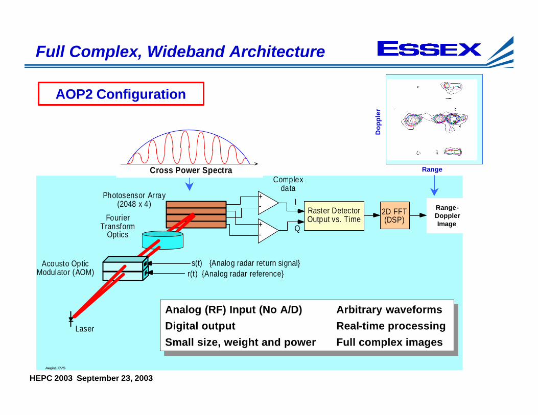
Full Complex, Wideband Architecture
Analog (RF) Input (No A/D) Arbitrary waveforms
Digital output Real-time processing
Small size, weight and power Full complex images
Analog (RF) Input (No A/D) Arbitrary waveforms
Digital output Real-time processing
Small size, weight and power Full complex images
Do
pp
ler
RangeCross Power Spectra
AOP2 Configuration
Range-Doppler Image

HEPC 2003 September 23, 200311
Optics Module Mated With Camera Module
Camera Card Connectors
Camera CardBragg Cell SMA Connectors
Optics Module
Optics Module Connector
Optics Processing Module
6U VME form factor

HEPC 2003 September 23, 200312
AOP2 Optics Module

HEPC 2003 September 23, 200313
System Calibrations and Corrections
• Calibrations and corrections are required at various points in the processing chain– Correct radar and processor response– Obtain optimum performance
RF Front End
Optical CPS
ReturnReference
RF Bragg data
(2, analog)
Camera data
CPS x phase
(2048, 4)
I/Q data
CPSI, CPSQ
(2048, 2)
Range compressed
images
RCII, RCIQ
(2048, 2)
Channel power Amplitude weighting Line phase correction
Deconvolutional filter
Range roll-Off
Range scale
Amplitude scale
Range Compression
FFT
I/Q Combine

HEPC 2003 September 23, 200314
AOP2 Hardware Configuration*
6U card cage- Controller card
- Optical module
- Post processing & Timing card
Power Meter
RF module
Power amplifiers
Programmable LOs for tunable RF front-end
Waveform generators
• Reference • Return
Real-time file system
UPS
* Including test equipment

HEPC 2003 September 23, 200315
AOP Production Conceptual Configuration
Size reduced from ½ rack in AOP2 demonstration to ½ single 6U chassis:
• AWGs reduced to single chip for PRN codes
• Synthesizers reduced to fixed LOs
• Amplifiers reduced to single card
• No output data storage, data sent to radar post processing in real time
OpticalReceiver RFFE Amps
Waveform generators
Amplifiers
RF front-end & LOs
Optical receiver
Camera & timing
Processing & control card
Controller
HEPC 2003 September 23, 200316
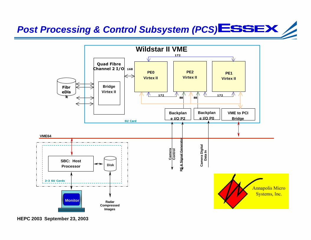
Post Processing & Control Subsystem (PCS)
VME64
6U Card
Cam
era
Dig
ital
Dat
a In
Cam
era
Co
ntr
ol
RF
& S
igna
l Gen
erat
or
PE1Virtex II
VME to PCI Bridge
Wildstar II VME
Backplane I/O P2
88 88172172
172
PE1Virtex II
Backplane I/O P0
Quad Fibre Channel 2 I/O
Bridge Virtex II
168
FibreDis
k
Monitor
DiskSBC: HostProcessor
RadarCompressed
Images
2-3 6U Cards
PE1Virtex II
PE0Virtex II
PE1Virtex II
PE2Virtex II
HEPC 2003 September 23, 200317
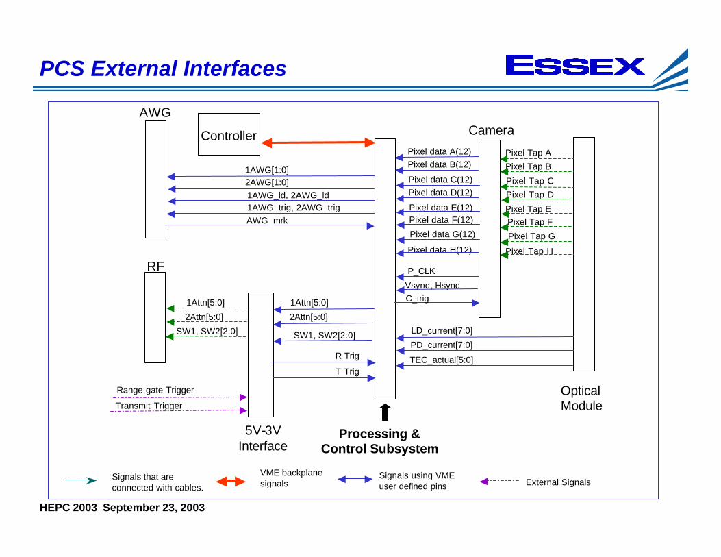
PCS External Interfaces
RF
Controller
Optical Module
Camera
Processing &Control Subsystem
P_CLK
Vsync, Hsync
Signals that are connected with cables.
External Signals
Pixel data A(12)Pixel data B(12)
Pixel data H(12)
5V-3VInterface
VME backplane signals
Pixel data C(12)Pixel data D(12)
Pixel data E(12)Pixel data F(12)
Pixel data G(12)
Signals using VME user defined pins
C_trig
Pixel Tap A
Pixel Tap B
Pixel Tap H
Pixel Tap C
Pixel Tap D
Pixel Tap EPixel Tap F
Pixel Tap G
TEC_actual[5:0]
1AWG[1:0]
Range gate Trigger
Transmit Trigger
R Trig
T Trig
SW1, SW2[2:0] PD_current[7:0]
LD_current[7:0]
AWG
2AWG[1:0]1AWG_ld, 2AWG_ld1AWG_trig, 2AWG_trigAWG_mrk
1Attn[5:0]
2Attn[5:0]
SW1, SW2[2:0]
1Attn[5:0]
2Attn[5:0]
HEPC 2003 September 23, 200318
WILDSTARTM II for VME
Copyright Annapolis Micro Systems, Inc. 2002
PE 2VIRTEX TM II
XC2V 6000, 8000
Backplane I/OP0
Backplane I/OP2
DDR2SRAM
2, 4 MB
36 DDR2SRAM
2, 4 MB
DDR2SRAM
2, 4 MB
36DDR2SRAM
2, 4 MB
DDR2SRAM
2, 4 MB
DDR2SRAM
2, 4 MB
36
36
36
ProgOsc
3
DDRSDRAM64 MB
32
88 88
PE 1VIRTEXTM II
XC2V 6000, 8000
I/O #1
DDR2SRAM
2, 4 MB
36 DDR2SRAM
2, 4 MB
DDR2SRAM
2, 4 MB
36DDR2SRAM
2, 4 MB
DDR2SRAM
2, 4 MB
DDR2SRAM
2, 4 MB
36
36
36
ProgOsc
3
DDRSDRAM64 MB
32
168
PE 0VIRTEXTM II
XC2V 6000, 8000
I/O #0
DDR2SRAM
2, 4 MB
36 DDR2SRAM
2, 4 MB
DDR2SRAM
2, 4 MB
36DDR2SRAM2, 4 MB
DDR2SRAM2, 4 MB
DDR2SRAM2, 4 MB
36
36
ProgOsc
3
DDRSDRAM64 MB
32
168
172 172
36 36 3636
VME BUS
PCIController
32/64 Bits 33/66 MHz
32 32 32
32 32
172
PCI to VME Bridge
Flash
Flash Flash Flash1616 16
MasterClock
Generator
PCLKMCLKICLK
16
DifferentialSingle Ended
Annapolis Micro Systems Wildstar II
FPGA based reconfigurable computing board

HEPC 2003 September 23, 200319
WILDSTARTM II for VME & Fibre Channel 2 I/O Card
WILDSTARTM II FPGA card Fibre Channel 2 I/O Card daughter card
HEPC 2003 September 23, 200320
Internal PCS Interfaces
PE2
• Collect Raw Data from detector
• Apply Correction
• Combine to get I & Q
• Update status for Controller
PE0
• Compute Range/Doppler Image
PE1
• Apply Correction to get CPS
• Compute Range Compressed Image
• Apply Correction to RCI
I & Q
CPS
CPS
RCI
Fibre Disk
RCI orRange/Doppler
CPS
Raw Camera Data

HEPC 2003 September 23, 200321
PE2 Data Processing
VME64
PA(11:0)
PB(11:0)
PC(11:0)
PD(11:0)
PE(11:0)
PF(11:0)
PG(11:0)
PH(11:0)
Pixel DataMemories
Camera CLK
Camera Controller
Controlsignals
I+(11:0)
I-(11:0)
Q+(11:0)
Q-(11:0)
H_syncV_sync
TriggerAmplitude WeightingMemories
X
X
X
X -
-
I(15:0)
Q(15:0)
I+(15:0)
I-(15:0)
Q+(15:0)
Q-(15:0)
System Controller
Signal Generation & RF Front End Signals
Controller Optical Module PCS Signal Generation and RF Front End Internal
Complex Data
Raw Data

HEPC 2003 September 23, 200322
PE2 Allocated Memory Diagram
Copyright Annapolis Micro Systems, Inc. 2002
PE 2VIRTEXTM II
XC2V 6000, 8000
Backplane I/OP0
Backplane I/OP2
DDR2SRAM
2, 4 MB
36 DDR2SRAM
2, 4 MB
DDR2SRAM
2, 4 MB
36DDR2SRAM
2, 4 MB
DDR2SRAM
2, 4 MB
DDR2SRAM
2, 4 MB
36
36
36
ProgOsc
3
DDRSDRAM64 MB
32
88 88
172 172
36
VME BUS
PCIController
PCI to VME Bridge
Flash
Flash
16
MasterClock
Generator
PCLKMCLKICLK
16
DifferentialSingle Ended
Direct connect to PE 1Direct connect to PE 0
Internal RAM: 16KB allocatediAmpWtTbl– 8192BqAmpWtTbl – 8192B
iRawPixelData – 2MB qRawPixelData – 2MB
iCalRawPixelData – 8KB qCalRawPixelData – 8KB

HEPC 2003 September 23, 200323
PE1 Functional Flow Diagram
PE2
Select Data
SourcedataSrcPE1
memClearPE1 Is memory full? Write Data to Memory
Apply Line Phase Correction
linePhErrMeasupdatedLPCorr
PE0Apply
Deconvolutional Filter and FFT
Window
decvFiltWdwVect
yes
no
Is memory full? Write Data to Memory
no
yesFFT Processing
PE0
updatedDeconv
upLP(0)
upDF(0)
Interleave I,Q
iRngImgData(31:0)qRngImgData(31:0)
cpsData(31:0)
iCorrectedPreFFT
qCorrectedPreFFT
iPixelData
qPixelData
PE2
iData(15:0)qData(15:0)

HEPC 2003 September 23, 200324
PE1 Allocated Memory Diagram
Copyright Annapolis Micro Systems, Inc. 2002
PE 1VIRTEXTM II
XC2V 6000, 8000
I/O #1
DDR2SRAM
2, 4 MB
36 DDR2SRAM
2, 4 MB
DDR2SRAM
2, 4 MB
36DDR2SRAM
2, 4 MB
DDR2SRAM
2, 4 MB
DDR2SRAM
2, 4 MB
36
36
36
ProgOsc
3
DDRSDRAM64 MB
32
168
172
36
VME BUS
PCIController
32/64 Bits 33/66 MHz
32
32
172
PCI to VME Bridge
Flash
Flash
16
MasterClock
Generator
PCLKMCLKICLK
16
DifferentialSingle Ended
Internal RAM: 24KB allocatedlinePhErrMeas – 8192BdecvFiltWdwVect – 8192BrangeRollOffVect – 8192BDirect connect to PE 0
Direct connect to PE 2
iPixelData – 1MB qPixelData – 1MB
iCorrectedPreFFT – 1MB qCorrectedPreFFT – 1MB
iRngImage – 2MB qRngImage – 2MB
HEPC 2003 September 23, 200325
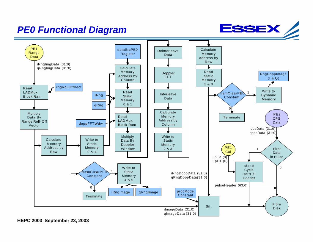
PE0 Functional Diagram
PE1RangeData
PE2CPSData
memClearPE0Constant
Write toStatic
Memory0 & 1
CalculateMemory
Address byColumn
ReadStatic
Memory0 & 1
CalculateMemory
Address byRow
ReadLADMuxBlock Ram
MultiplyData ByDopplerWindow
DopplerFFT
CalculateMemory
Address byColumn
memClearPE0Constant
Terminate
0
1
DeinterleaveData
InterleaveData
rngRollOffVect
iRngImage qRngImage
doppFFTWdw
Terminate
Write toStatic
Memory2 & 3
RngDoppImage( I & Q)
dataSrcPE0Register
ReadLADMuxBlock Ram
MultiplyData By
Range Roll -OffVector
Write toStatic
Memory4 & 5
0
1
CalculateMemory
Address byRow
ReadStatic
Memory2 & 3
FirstData
in Pulse
1
0
Write toDynamicMemory
iRng
qRng
iRngImgData (31:0)qRngImgData (31:0)
icpsData (31:0)qcpsData (31:0)
iRngDoppData (31:0)qRngDoppData(31:0)
iImageData (31:0)qImageData (31:0)
pulseHeader (63:0)
MakeCycle
Cnt/CalHeader
PE1Cal
upLP (0)upDF (0)
Sift
procModeConstant
FibreDisk

HEPC 2003 September 23, 200326
PE0 Allocated Memory Diagram
Copyright Annapolis Micro Systems, Inc. 2002
PE 0VIRTEXTM II
XC2V 6000, 8000
I/O #0
DDR2SRAM
2, 4 MB
36 DDR2SRAM
2, 4 MB
DDR2SRAM
2, 4 MB
36DDR2SRAM2, 4 MB
DDR2SRAM2, 4 MB
DDR2SRAM2, 4 MB
36
36
ProgOsc
3
DDRSDRAM64 MB
32
168
172
36 36
VME BUS
PCIController
32/64 Bits
32
32
PCI to VME Bridge
Flash
Flash
16
MasterClock
Generator
PCLKMCLKICLK
16
DifferentialSingle Ended
172 Direct connect to PE 1
Direct connect to PE 2
iRng0 – 2MB
iRngDoppImage – 2MB
qRng0 – 2MB
qRngDoppImage – 2MB
Internal RAM: 2KB allocatediDoppFFTWdw – 1024BqDoppFFTWdw – 1024B
RngDopp – 8MB
iRng1 – 2MB qRng1 – 2MB

HEPC 2003 September 23, 200327

HEPC 2003 September 23, 200328
Corefire Example

HEPC 2003 September 23, 200329
PCS Testing: CoreFire Debugger
CoreFireTM Application Debugger includes windows for monitoring and manipulating data flow

HEPC 2003 September 23, 200330
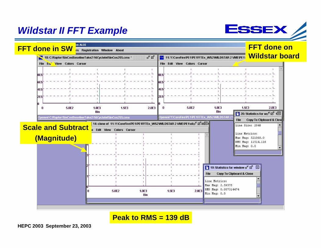
Wildstar II FFT Example
FFT Example Scenario• CoreFire project for PE1
Data read from memory on Wildstar II boardFFT operationData written to memory on Wildstar II board
• Java programData read from fileData written to memory on Wildstar II boardData read from memory on Wildstar II boardData written to file
• CoreFire DebuggerKicks off the Wildstar II board processingMemory and register viewers show data during the processing
• IView ToolCompare output data file with expected results
HEPC 2003 September 23, 200331
Wildstar II FFT Example
Peak to RMS = 139 dB
FFT done in SW FFT done on Wildstar board
Scale and Subtract(Magnitude)
HEPC 2003 September 23, 200332
Conclusions
• Essex has been able to implement an extremely complex, computationally intensive radar processing task in:– Embedded optical hardware and– Embedded DSP/FPGA hardware
• This approach saves space, development time, software, development costs and maintenance costs.
• The AOP hardware allows the use of new arbitrary classes of waveforms for improved ballistic missile discrimination.

HEPC 2003 September 23, 200333
Wrap-up / Questions