Embed Size (px)
Citation preview

HAL Id: hal-01886795https://hal.archives-ouvertes.fr/hal-01886795
Submitted on 3 Oct 2018
HAL is a multi-disciplinary open accessarchive for the deposit and dissemination of sci-entific research documents, whether they are pub-lished or not. The documents may come fromteaching and research institutions in France orabroad, or from public or private research centers.
L’archive ouverte pluridisciplinaire HAL, estdestinée au dépôt et à la diffusion de documentsscientifiques de niveau recherche, publiés ou non,émanant des établissements d’enseignement et derecherche français ou étrangers, des laboratoirespublics ou privés.
High-Frequency Model of the Coupled Inductors Usedin EMI Filters
Jean-Luc Kotny, Xavier Margueron, Nadir Idir
To cite this version:Jean-Luc Kotny, Xavier Margueron, Nadir Idir. High-Frequency Model of the Coupled InductorsUsed in EMI Filters. IEEE Transactions on Power Electronics, Institute of Electrical and ElectronicsEngineers, 2012, 27 (6), pp.2805 - 2812. �10.1109/TPEL.2011.2175452�. �hal-01886795�

1
Jean-Luc Kotny1,2, Xavier Margueron1,3, Member, IEEE, and Nadir Idir1,2, Member, IEEE 1 Univ Lille Nord de France, F-59000 Lille, France
2 USTL, L2EP, F-59650 Villeneuve d’Ascq, France 3 ECLille, L2EP, F-59650 Villeneuve d’Ascq, France
Dr Jean-Luc Kotny Université de Lille 1 Laboratoire L2EP – Bât. P2 – Cité Scientifique F-59655 Villeneuve d'Ascq Cedex -FRANCE Tel. 33 (0)320.43.48.62 - Fax. 33 (0)320.43.69.67 Email: [email protected] Dr Xavier Margueron Ecole Centrale de Lille – L2EP Cité Scientifique F-59651 Villeneuve d'Ascq Cedex -FRANCE Tel. 33 (0)320.33.53.88 - Fax. 33 (0)320.33.54.54 Email: [email protected] Prof Nadir Idir Université de Lille 1 Laboratoire L2EP – Bât. P2 – Cité Scientifique F-59655 Villeneuve d'Ascq Cedex -FRANCE Tel. 33 (0)320.33.77.90 - Fax. 33 (0)320.43.69.67 Email: [email protected] Paper has been presented at conference :
- IEEE Energy Conversion Congress and Exposition – ECCE’09.
Abstract— This paper deals with a high frequency modeling method of the coupled inductors used in EMI filters.
These filters are intended to reduce conducted emissions generated by power static converters towards the power grid.
To model the EMI filters, it is necessary to identify the various parameters of the passive elements: inductors and
capacitors. Because of their major impact on filter efficiency, these elements must be identified with accuracy. In this
study, high frequency model of common mode coupled inductors is proposed. The identification of the model parameters
is based on the experimental approach. Simulation results of the proposed model are compared to the experimental data
obtained using the specific experimental setup. These results made it possible to validate the EMI filter model and its
robustness in a frequency range varying from 9 kHz to 30 MHz. The proposed high frequency inductor models will be
very helpful for design and optimization of EMI filters, since the high frequency behavior of the filter mainly depends on
magnetic materials used and on the geometrical characteristics of winding.
High Frequency Model of the coupled inductors used in EMI Filters

2
I. INTRODUCTION
Nowadays, the increase of power converter number is very problematic for electromagnetic compatibility (EMC). Indeed,
each power static converter generates a lot of high frequency (HF) interferences toward the power network which becomes more
and more polluted [1]. The main solution to reduce these conducted emissions is based on the utilization of EMI filters [2]-[3]. It
can also be combined with other solutions like the slowing down the dv/dt and di/dt during the transitions of the power semi-
conductor components and/or by acting on the converter controls [4]-[5].
The EMI filters are made of coupled inductors combined with capacitors; the choice of the topology depends on network and
load impedances. A typical differential mode (DM) and common mode (CM) filter used for power converter is shown in Fig.1.
Fig. 1. Typical EMI Filter topology
It is well-known that magnetic components have a strong impact on filter efficiency [6]-[7]. They are typically made with
copper wiring on high permeability ring ferrite. These chokes are traditionally designed by a "cut and try" process, which is very
expensive and time consuming because of the high number of prototypes which are needed. Wires specifications and their
placement, PCB characteristics, or magnetic core performances introduce parasite effects that can reduce drastically the filter's
efficiency [8]-[9].
The stray elements of the passive components, such as equivalent series inductor (ESL) of capacitors and equivalent parallel
capacitor (EPC) of inductors, degrade the performances of the EMI filters. While for a lot of cases, their influence is less
important than the couplings among components and layouts [10].
In order to design and optimize the performance of the filter by simulation, a high frequency model, including parasitic
elements, must be used. These elements must be identified with a good accuracy [11]. In this paper, a high frequency modelling
method of the coupled inductors of EMI filter is presented. The new equivalent circuit is detailed and its characterisation process
is described. The obtained model is tested with different magnetic material and gives good results on a large frequency range
from 1 kHz to 30 MHz. In order to validate the proposed model and to test its reliability, a common mode inductors and

3
capacitors are used to realise an EMI filters. The simulation results using the high frequency model of the filter are validated by
experimental measurements. In the following section, high frequency modelling method of the coupled inductors is detailed.
II. HIGH FREQUENCY MODEL OF COUPLED INDUCTORS
In this study, a prototype of the coupling inductors has been realized with EPCOS ferrite material N30 [12]. The core shape is a
ring R58.3/40.8/17.6 and each winding is made of 15 turns of copper (diameter 1.5mm). At first, we will propose an equivalent
circuit model of the coupled inductors. Then, we propose an experimental method of characterization of the passive component
which will enable to identify the model parameters.
A. Equivalent Circuit of the coupled inductors
Coupled inductors used in EMI filters are a specific case of traditional n-windings magnetic components [13]-[14] because
they are made with two identical windings around a magnetic core (Fig. 2a). The objective is to have a model of coupled
inductors based on equivalent electrical circuit that enable to describe the various physical phenomena (magnetic and
electrostatic) which appear in high frequency. In order to have a more precise model, a symmetrical equivalent circuit of these
inductors, is used (Fig. 2b). The proposed model is a lumped model; it uses only R, L, and C elements to describe its behaviour
in a large frequency range. Half of the equivalent circuit is made of three impedances Z1 (x2) and Z2, an ideally coupled inductors
and four different capacitors CS, Ce, CP, CC.
(a): Common mode inductors
(b): High frequency equivalent circuit
Fig. 2. High frequency model of the coupled inductors

4
It is known that for a 2-windings transformer model, with a strong magnetic coupling, only three capacitors are necessary to
describe its electrostatic behaviour [14]. In the case of the coupled inductors and in order to have a symmetric model (for each
winding), a supplementary capacitor CS has been added to the circuit as shown in Fig. 2b.
B. Parameters identification method
In order to determine the parameters of the common mode inductors model (Fig 2b), impedance measurements realized in
different test configurations are necessary. An impedance analyzer (Agilent 4294A) is then used and it enables to obtain
impedance measurements (modulus and phase) on a large frequency range from 1 kHz to 100 MHz [15].
To identify the various impedances of magnetic component, different test configurations can be carried out [16]. Due to the
geometrical symmetry of coupled inductors and using the equivalent circuit presented in the Fig. 2b, only five well-chosen
measurements, as shown in Fig. 3, should be sufficient for determine all the magnetic and electrostatic parts of the model.
In order to determine all the parameters of the coupled inductors model, different kind of impedance are necessary. For
example, subtracting flux or additional flux measurements are realized and only one open circuit measurement is used for the
magnetizing inductance identification. Figure 3 describes the main five measurement configurations (T0 until T4) that are chosen
to identify the equivalent circuit elements of the coupled inductors.
In the determination process of the model parameters, the first configuration T0 is used to identify the leakage impedance 1Z .
Then, T0, T1, T2 and T3 are combined to calculate the four capacitances and finally T4 enables to identify the magnetizing part of
the component. The Table I sum up the various measurement configurations which allow to identify the model parameters. The
five impedances measured on the prototype using the impedance analyzer are shown in Figures 4 and 5.
(a): Parallel windings Subtracting flux (T0)
(b): Series windings Subtracting flux (T1)
(c): Parallel windings Additional flux (T2)
(d): Between e1 and e2 with two short circuits (T3)
(e): Open circuit (T4)
Fig. 3. Impedance measurement configurations
TABLE I MODEL PARAMETERS IDENTIFICATION

5
Fig. 4. Impedance (modulus) measurement configurations (T0, T1, T4)
Fig. 5. Impedance (modulus) measurement configurations (T2 ,T3)
The impedance measured in configuration T3 is quite different from the others because it corresponds to a capacitive behaviour
from 1 KHz to 30 MHz. Indeed, this impedance is measured between both windings short circuited so the measurement is
equivalent to a capacitance.
III. DETERMINATION OF THE MODEL PARAMETERS
All impedances are modeled by one or more combination of RLC circuit. The aim of this section is to propose equivalent
circuits which allow to model the frequency variation of leakage impedance ( 1Z ), magnetizing impedance ( 2Z ) and the 4
capacitors ( cC , eC , pC and sC ) of the coupled inductors shown in Fig. 2b.
A. Leakage Impedance
The leakage impedance parameters are obtained from the measurement configuration T0 because windings are connected in a
subtracting flux topology (cancellation of magnetizing flux). The impedance obtained from T0 corresponds to parallel RLC
impedance which the equivalent circuit is shown in Fig. 6. The inductance 1L is identified in frequency band (between 1 kHz

6
and 3.7 MHz) when the impedance measured in this configuration increases (and phase equal to 90°). The inductance variation
(with frequency) is due to eddy current effects in the copper wires. Until the resonance frequency, the error between the model
and the measurement is still lower than 5%. The obtained model is quite simple but can be improved using ladder RL circuits in
order to model correctly the eddy current effects [14]. The value of the resistance R1 is measured at the resonance frequency
( MHzfr 9.19 ) of the impedance obtained from T0 as shown in Fig. 4. The capacitance of the equivalent circuit of the coupled
inductor in configuration T0 is given by )(20 CpCC e .
Fig. 6. Equivalent circuit of the measurement configuration (T0)
From the curve (T0) shown in Fig. 4, the capacitance 0C is computed from the resonance frequency ( MHzfr 9.19 ) using
equation (1). This capacitance corresponds to the combination of both capacitances eC and pC . The table II sums up these
leakage parameter values.
1.2
).2(
10
Lrf
C
(1)
TABLE II LEAKAGE PARAMETERS
B. Parasitic Capacitances
The capacitance value C0 is identified from the leakage impedance measured in configuration T0. However, it remains three
other capacities to calculate. With three more equations, the system can be solved. These equations are given by measurements
carried out in configurations T1, T2 and T3. Their equivalent circuits are presented in Fig. 7.

7
(a): configuration (T1) (b): configuration (T2) (c): configuration (T3)
Fig. 7. Equivalent circuit of three measurement configurations
The impedance measured in configuration T1 is quite similar to T0. Thus, the model used is also a parallel RLC circuit
(Fig.7a). The measured values of R and L are four times higher than the leakage parameters. The capacitance value C1 is also
determined from the resonance frequency. The value of this capacitance is given by the following relation:
pFCC
CCC eCpS 8.6
21
(2)
The equivalent circuit of the impedance measured in configuration T2 cannot use only one RLC series circuit. Indeed, one
will show, in the next section, that the magnetizing impedance will require three RLC circuits to describe its high frequency
behaviour. Because the focus is on the electrostatic part of the impedance, for frequency upper than 50MHz, a tangent of the
impedance curve is plotted. The obtained equivalent capacitance is equal to:
pFCCC Ce 8)(22 (3)
The last needed equation is given by impedance measured in the configuration T3. Its equivalent representation is a RLC series
circuit shown in the Fig.7c. The capacitance is easily evaluated between 1 kHz and 4 MHz using the imaginary part of the
measured impedance. The equivalent capacitance is equal to:
pFCCCC SCP 2.19)(23 (4)
Finally, these measurements lead to a 4-unknown equations system (5) that can be easily solved and the obtained results are
given in (6).
3
2
1
0
222
2222
22
CCsCpCc
CCcCe
CCsCpCeCc
CCpCe
(5)

8
22
2
242
24
24
31
0
321
0
321
321
CC
CCs
CCC
CCp
CCCCe
CCCCc
(6)
The table III sums up the obtained values for the four capacitances.
TABLE III CAPACITOR VALUES
One can note that the value of the capacity Ce is negative. This can be justified by the simplicity of the proposed behaviour
model of the impedances and also to the measurement errors related to the accuracy of the impedance analyzer (measurement
equipment).
C. Magnetizing Impedance
The impedance measured in configuration T4 enables to characterize the magnetizing part Z2 of the component. Thus, such
impedance, shown in Fig. 8, cannot be described by only one RLC circuit. Three different circuits have to be used in order to
describe the three areas.
Fig. 8. Impedance modulus in open circuit (configuration (T4))
- The first area, from low frequency to F1 = 670 kHz, corresponds to the proper inductance traditionally calculated using the
following relation:
LANL 2 (7)
With:
N: winding turns,
9
AL: inductance factor. The inductance factor of the ferrite material N30, used to realized a prototype of the coupling inductors, is equal to AL =5400 ±
20%. Thus, it's well known that the characteristics of magnetic materials used in the design of the EMI filters depend on the
levels and frequencies ranges of the conducted disturbances to be attenuated.
- The second area, from F1 to F2 = 11 MHz, corresponds to high frequency effects of the magnetic material. This frequency
band is divided into two parts 2a and 2b. At the frequency F’2, one can note a slope break of the impedance modulus, thus, the
magnetic material effect is masked by an electrostatic effect.
- In the third area, a resonance appears which can be linked to the inductive leakage phenomena combined with electrostatic
effects.
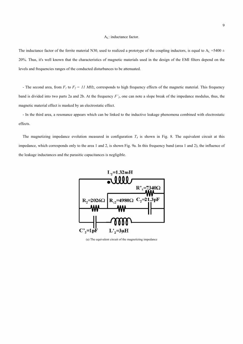
The magnetizing impedance evolution measured in configuration T4 is shown in Fig. 8. The equivalent circuit at this
impedance, which corresponds only to the area 1 and 2, is shown Fig. 9a. In this frequency band (area 1 and 2), the influence of
the leakage inductances and the parasitic capacitances is negligible.
(a) The equivalent circuit of the magnetizing impedance

10
(b) Comparison of the impedance modulus in configuration (T4)
Fig. 9. Modelling of the magnetizing impedance
The value of L2 is calculated using the imaginary part of the impedance (L2 = Z2 sin ) in the frequency band between 1
KHz and 370 kHz as shown in the Fig. 8 (or using relation (7)) . The obtained value of this inductance is equal to L2 = 1.32mH.
The elements R'2 and C2 are obtained from the first resonance frequency F1 =670 KHz (Fig. 8). The resistance value is equal
to R'2 = 7340. The capacitance 2C is calculated with the following relation:
pF
FLC 4.21
22
12
122
(8)
The elements R2 and RC2 fix the impedance slope between the frequencies F1 and F'2 (area 2a). The value of the resistance RC2
= 4980 is obtained from the impedance slope in this area. However, the resistance R2 is calculated using the equivalent
resistance at the frequency F'2 =3 MHz. Its value is equal to R2 = 2026.
The last equivalent circuit L'2 and C'2 is used to model the evolution of the impedance between F'2 and F2 (area 2b). The
values of these parameters are obtained by a fitting method using APLAC software. In order to show the influence of the various
elements on the accuracy of the proposed model, we present in Fig. 10a the comparison between a simulation of the equivalent
circuit of the magnetizing impedance without elements R2 and RC2. However, Fig. 10b show the simulation of the same circuit
without elements L’2 and C’2.

11
(a): Influence of R2 and Rc2
(b): Influence of L’2 and C’2
Fig. 10. Model of the magnetizing impedance
The comparison between simulation results and measurement data (Fig 9b) shows that the proposed equivalent circuit allows
to model, with a good accuracy, the evolution of the magnetizing impedance Z2. Figure 11 presents the final high frequency
coupled inductors model. Its parameter values are listed in the Table IV. The obtained model uses only electrical equivalent
circuits that enable to make simulations in frequency and time domains using simulator software such as SPICE. However, for
time domain simulation, negative capacitances must be removed to positive one using inverse perfect couplers [14].
Fig. 11. High frequency model of the coupled inductors

12
TABLE IV EQUIVALENT CIRCUIT COMPONENT VALUES
To complete the equivalent circuit, supplementary resistors Rc is added in series with impedance Z1 in order to model the low
frequency winding resistance which measured with impedance analyzer. The validity of the obtained model will be discussed in
the following section.
IV. MODEL VALIDATION
To validate the proposed model, different configuration tests are considered. To study the robustness of the model, two other
configurations: short circuit measurements T5, open circuit T6 as shown in Fig. 12 are used. The comparison between
experimental data and simulation results, using SPICE software, is shown in Fig. 13. The obtained results show a good accuracy
of the coupled inductors model up to 100 MHz. These results prove the validity and robustness of the proposed model. The next
step consists to use the proposed model to study by simulation the design of the EMI filter which is made from common mode
and differential mode filters.
(a): Short-circuit of one winding (T5)
(b): open circuit with e1-s2 connected (T6)
Fig. 12. Impedance measurement configurations

13
(a) : Configuration T5 (b) : Configuration T2
(c) : Configuration T0 (d) : Configuration T6 Fig. 13. Impedance evolution of the coupled inductors in four configuration tests (simulation and experimental)
V. EMI FILTER APPLICATION
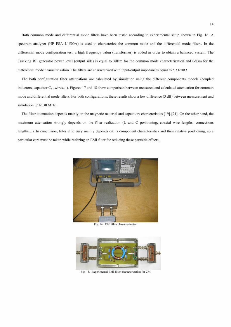
The coupled inductors are associated with capacitors to achieve a complete EMI filter. Components are connected together on
the PCB and placed inside a metallic box as shown in Fig. 14. Figure 15 shows the interior of the box which contains the
common mode inductors and four capacitors CY = 4,7nF. The two small boxes are the resistive dispatchers which used to divide
the power injected in an equal way on the two inputs ports of the filter. For simulation, the capacitors “CY” have been
characterized using the impedance analyzer. The equivalent circuit used is a RLC series circuit: nFC 9.4 , 18.0R ,
.4.6 nHR The connection wires were also modeled [17]-[18].
14
Both common mode and differential mode filters have been tested according to experimental setup shown in Fig. 16. A
spectrum analyzer (HP ESA L1500A) is used to characterize the common mode and the differential mode filters. In the
differential mode configuration test, a high frequency balun (transformer) is added in order to obtain a balanced system. The
Tracking RF generator power level (output side) is equal to 3dBm for the common mode characterization and 0dBm for the
differential mode characterization. The filters are characterised with input/output impedances equal to 50/50.
The both configuration filter attenuations are calculated by simulation using the different components models (coupled
inductors, capacitor CY, wires…). Figures 17 and 18 show comparison between measured and calculated attenuation for common
mode and differential mode filters. For both configurations, these results show a low difference (3 dB) between measurement and
simulation up to 30 MHz.
The filter attenuation depends mainly on the magnetic material and capacitors characteristics [19]-[21]. On the other hand, the
maximum attenuation strongly depends on the filter realization (L and C positioning, coaxial wire lengths, connections
lengths…). In conclusion, filter efficiency mainly depends on its component characteristics and their relative positioning, so a
particular care must be taken while realizing an EMI filter for reducing these parasitic effects.
Fig. 14. EMI filter characterization
Fig. 15. Experimental EMI filter characterization for CM

15
(a): Common Mode filter (b): Differential Mode filter
Fig. 16. Measurement method of the CM and DM filters attenuations
Fig. 17. Common mode filter response. Tracking generator power level (output) is equal to 3dBm
Fig. 18. Differential mode filter response. Tracking generator power level (output) is equal to 0dBm
VI. CONCLUSION
In this paper, an electrical equivalent circuit of coupled inductors used in EMI filters is detailed. The symmetric model
proposed takes into account of the high frequency phenomena which appear when the frequency increase. The identification
method of the model parameters using impedance measurements in different configurations tests has been proposed. The
obtained model has been tested and validated for common mode inductors. The proposed model of the coupled inductors is used
in the simulation of EMI filter. The obtained results show very good agreement between a simulation results and experimental

16
data up to 30 MHz. The next work consists to optimise the EMI filters (Weight, dimensions …) by simulation using the proposed
EMI filter model associated to the high frequency models of the power converters and Line Impedance Stabilisation Network.
REFERENCES
[1] S. Wang, Y. Y. Maillet, F. Wang. D. Boroyevich, R. Burgos, "Investigation of Hybrid EMI Filters for Common-Mode EMI Suppression in a Motor Drive
System," IEEE Transactions on Power Electronics, Vol.25, N° 4, April 2010, pp.1034-1045.
[2] H. Akagi, H. Hasegawa, T. Doumoto, "Design and performance of passive EMI Filter For Use with A Voltage-Source PWM Inverter Having Sinusoidal
Output Voltage And Zero Common-Mode Voltage", IEEE Transactions on Power Electronics, Vol.19, N° 4, July 2004, pp.1069-1076.
[3] W. Xiaofeng, X. Dehong, Z. Yanjun, C. Yi, O. Yasuhiro, M. Kazuaki, "Integrated EMI Filter Design with Flexible PCB Structure", IEEE Power
Electronics Society, PESC08, Rhodes, Greece, June 15-19 2008, CD proceeding, pp. 1613-1617.
[4] N. Idir, R. Bausière, J. J. Franchaud, "Active gate voltage control of turn-on di/dt and turn-off dv/dt in insulated gate transistors", IEEE Transactions on
Power Electronics, Vol. 21-4, july 2006, pp.849-855.
[5] A. Videt, P. Le Moigne, N. Idir, P. Baudesson, X. Cimetiere, "A New Carrier-Based PWM Providing Common-Mode-Current Reduction and DC-Bus
Balancing for Three-Level Inverters", IEEE Transactions on Industrial Electronics, Vol.54, N° 6, december 2007.
[6] H. Chen, Z. Qian, Z. Zeng and C. Wolf, "Modeling of parasitic inductive couplings in a Pi-shaped common mode EMI filters", IEEE Trans. on
Electromagnetic Compatibility, Vol.50, N° 1, February 2008.
[7] R. Chen, J. D. Van Wyk,S. Wang, W. G. Odendaal, "Improving the Characteristics of Integrated EMI Filters by Embedded Conductive Layers", IEEE
Transactions on Power Electronics, Vol. 20, No. 3, May 2005.
[8] X. Wu, D. Xu, Z. Wen, Y. Okuma, K. Mino, "Design, Modeling, and Improvement of Integrated EMI Filter With Flexible Multilayer Foils," IEEE
Transactions on Power Electronics, Vol.26, N°.5, May 2011, pp.1344-1354.
[9] F. Leferink, H. Bergsma, B. Ferreira, W. Van Etten, “High Performance EMI Filter for Frequency Converters”, EMC Europe 2004, Eindhoven.
[10] Shuo Wang, F.C. Lee, D.Y. Chen and W.G. Odendaal, “Effects of Parasitic Parameters on the Performance of EMI Filters”, IEEE Trans. on Power
Electronics, Vol. 19, May. 2004, pp. 869 –877.
[11] S. Wang, F. C. Lee, W. G. Odendaal, " Characterization and Parasitic Extraction of EMI Filters Using Scattering Parameters", IEEE Transactions on Power
Electronics, Vol. 20, N° 2, March 2005.
[12] http://www.epcos.com/web/generator/Web/Sections/ProductCatalog/Ferrites/
[13] X. Margueron, J-P. Keradec, "Design of Equivalent Circuits and Characterization Strategy for n-Input Coupled Inductors", IEEE Transaction on Industry
Applications, Vol.43, N°1, Jan./Feb. 2007, pp.14-22.
[14] X. Margueron, J-P. Keradec, "Identifying the Magnetic Part of the Equivalent Circuit of n-Winding Transformer", IEEE Transactions on Instrumentation
and Measurement, Vol.56, N° 1, February 2007, pp.146-152.
[15] Agilent 4294A Precision Impedance Analyzer-Operation Manual, Agilent Technologies.
[16] S.Wang, F. Lee,W. Odendaal, and J. vanWyk, “Improvement of EMI filter performance with parasitic coupling cancellation,” IEEE Transactions on Power
Electronics., vol. 20, no. 5, pp. 1221–1228, Sep. 2005.
[17] G. Grandi, I.Montanari, and U. Reggiani, “Effects of power converter parasitic components on conducted EMI,” in Proc. Int. Symp. Electromagn. Compat.
(EMC Zurich), 1997, pp. 499–504.

17
[18] H. Zhu, A. Hefner, Jr., and J. Lai, “Characterization of power electronics system interconnect parasitics using time domain reflectometry,” IEEE Trans.
Power Electron., Vol. 14, N° 4, pp. 622–628, Jul. 1999.
[19] T. C. Neugebauer and D. J. Perreault, “Parasitic capacitance cancellation in filter inductors,” IEEE Transactions on Power Electronics, vol. 21, no. 1, pp.
282–288, Jan. 2006.
[21] M. C. Caponet, F. Profumo, A. Tenconi, A., “EMI filters design for power electronics,” Power Electronics Specialists Conference, 2002. pesc 02. 2002
IEEE 33rd Annual, Vol. 4, 23-27 June 2002, pp. 2027 – 2032.
[22] Y. Maillet, L. Rixin, W. Shuo, W. Fei, R. Burgos, D. Boroyevich, "High-Density EMI Filter Design for DC-Fed Motor Drives," Power Electronics, IEEE
Transactions on Power Electronics, Vol.25, N°.5, May 2010, pp.1163-1172.
Jean-Luc Kotny received the Ph.D. degree from the University of Lille 1, France, in 1984. He is currently an Assistant Professor with the University of Lille 1. His main research interests include power electronics and electromagnetic compatibility.
Xavier Margueron (M’09) was born in Chambery, France, in 1980. He received the Diploma in electrical engineering from the Ecole Nationale Supérieure d’Ingénieurs Electriciens de Grenoble, Grenoble, France, in 2003, and the Doctorat de Génie Electrique from the Université Joseph Fourier, Grenoble, in 2006. Its principal fields of research related to passive components and HF modelling. Since September 2007, he has been an associate professor at the Ecole Centrale de Lille, France, where he carries out research in the L2EP laboratory. His research interests are HF power electronics and passive component modelling and optimization.
Nadir Idir (M'07) received the Ph.D. degree from the University of Lille, France, in 1993. He is currently a Professor with the Laboratory of Electrical Engineering and Power Electronics (L2EP) of the University of Lille. His main research interests include power electronics and electromagnetic compatibility.


![DEVELOPMENT OF BUCK-BOOST CONVERTER TO ACHIEVE HIGH … · 2019-01-10 · inductors is potentially beneficial [4]. The coupled inductors also offer additional benefits such as](https://img.dokumen.tips/doc/110x75/5f4d972568593756d475e481/development-of-buck-boost-converter-to-achieve-high-2019-01-10-inductors-is-potentially.jpg)


