Embed Size (px)
Citation preview
LED Engin | 651 River Oaks Parkway | San Jose, CA 95134 USA | ph +1 408 922 7200 | fax +1 408 922 0158 | em [email protected] | www.ledengin.com
COPYRIGHT © 2018 LED ENGIN. ALL RIGHTS RESERVED. LZ1-00DB00 (6.0 – 05/11/18)
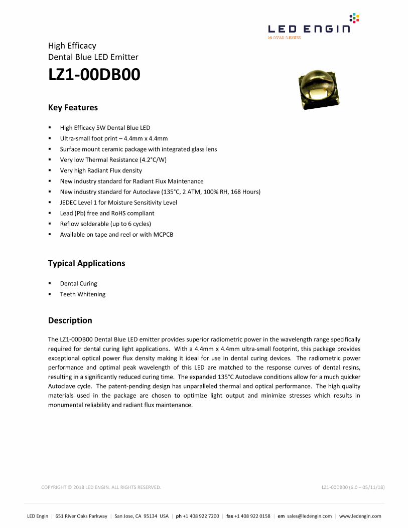
High Efficacy Dental Blue LED Emitter
LZ1-00DB00
Key Features
High Efficacy 5W Dental Blue LED
Ultra-small foot print – 4.4mm x 4.4mm
Surface mount ceramic package with integrated glass lens
Very low Thermal Resistance (4.2°C/W)
Very high Radiant Flux density
New industry standard for Radiant Flux Maintenance
New industry standard for Autoclave (135°C, 2 ATM, 100% RH, 168 Hours)
JEDEC Level 1 for Moisture Sensitivity Level
Lead (Pb) free and RoHS compliant
Reflow solderable (up to 6 cycles)
Available on tape and reel or with MCPCB
Typical Applications
Dental Curing
Teeth Whitening
Description
The LZ1-00DB00 Dental Blue LED emitter provides superior radiometric power in the wavelength range specifically
required for dental curing light applications. With a 4.4mm x 4.4mm ultra-small footprint, this package provides
exceptional optical power flux density making it ideal for use in dental curing devices. The radiometric power
performance and optimal peak wavelength of this LED are matched to the response curves of dental resins,
resulting in a significantly reduced curing time. The expanded 135°C Autoclave conditions allow for a much quicker
Autoclave cycle. The patent-pending design has unparalleled thermal and optical performance. The high quality
materials used in the package are chosen to optimize light output and minimize stresses which results in
monumental reliability and radiant flux maintenance.

2
LED Engin | 651 River Oaks Parkway | San Jose, CA 95134 USA | ph +1 408 922 7200 | fax +1 408 922 0158 | em [email protected] | www.ledengin.com
COPYRIGHT © 2018 LED ENGIN. ALL RIGHTS RESERVED. LZ1-00DB00 (6.0 – 05/11/18)
Part number options
Base part number
Part number Description
LZ1-00DB00-xxxx LZ1 emitter
LZ1-10DB00-xxxx LZ1 emitter on Standard Star MCPCB
LZ1-30DB00-xxxx LZ1 emitter on Miniature round MCPCB
Bin kit option codes
DB, Dental-Blue (460nm)
Kit number suffix
Min flux Bin
Color Bin Range Description
0100* L D1 – D1 full distribution flux; full distribution wavelength
* Previous version was -0000, please refer to Mechanical Dimensions section on p.6, PCN 54-2 and 55 for more details.

3
LED Engin | 651 River Oaks Parkway | San Jose, CA 95134 USA | ph +1 408 922 7200 | fax +1 408 922 0158 | em [email protected] | www.ledengin.com
COPYRIGHT © 2018 LED ENGIN. ALL RIGHTS RESERVED. LZ1-00DB00 (6.0 – 05/11/18)
Radiant Flux Bins
Table 1:
Bin Code
Minimum
Radiant Flux (Φ)
@ IF = 1000mA
[1,2]
(mW)
Maximum
Radiant Flux (Φ)
@ IF = 1000mA
[1,2]
(mW)
L 800 1000
M 1000 1250
Notes for Table 1: 1. Radiant flux performance is measured at specified current, 10ms pulse width, Tc = 25
oC. LED Engin maintains a tolerance of ± 10% on flux measurements.
Peak Wavelength Bin
Table 2:
Bin Code
Minimum
Peak Wavelength (λP)
@ IF = 1000mA
[1]
(nm)
Maximum
Peak Wavelength (λP)
@ IF = 1000mA
[1]
(nm)
D1 457 463
Notes for Table 2:
1. Peak wavelength is measured at specified current, 10ms pulse width, Tc = 25oC. LED Engin maintains a tolerance of ± 2.0nm on peak wavelength
measurements.
Forward Voltage Bin
Table 3:
Bin Code
Minimum
Forward Voltage (VF)
@ IF = 1000mA
[1]
(V)
Maximum
Forward Voltage (VF)
@ IF = 1000mA
[1]
(V)
0 3.20 4.40
Notes for Table 3: 1. Forward voltage is measured at specified current, 10ms pulse width, Tc = 25
oC. LED Engin maintains a tolerance of ± 0.04V for forward voltage measurements.

4
LED Engin | 651 River Oaks Parkway | San Jose, CA 95134 USA | ph +1 408 922 7200 | fax +1 408 922 0158 | em [email protected] | www.ledengin.com
COPYRIGHT © 2018 LED ENGIN. ALL RIGHTS RESERVED. LZ1-00DB00 (6.0 – 05/11/18)
Absolute Maximum Ratings
Table 4:
Parameter Symbol Value Unit
DC Forward Current at Tjmax=135°C [1] IF 1200 mA
DC Forward Current at Tjmax=150°C [1] IF 1000 mA
Peak Pulsed Forward Current
[2] IFP 2000 mA
Reverse Voltage VR See Note 3 V
Storage Temperature Tstg -40 ~ +150 °C
Junction Temperature TJ 150 °C
Soldering Temperature
[4] Tsol 260 °C
Allowable Reflow Cycles 6
Autoclave Conditions 135°C at 2 ATM,
100% RH for 168 hours
ESD Sensitivity
[5] > 8,000 V HBM
Class 3B JESD22-A114-D
Notes for Table 4: 1. Maximum DC forward current is determined by the overall thermal resistance and ambient temperature. Follow the curves in Figure 10 for current derating. 2: Pulse forward current conditions: Pulse Width ≤ 10msec and Duty Cycle ≤ 10%. 3. LEDs are not designed to be reverse biased. 4. Solder conditions per JEDEC 020D. See Reflow Soldering Profile Figure 3. 5. LED Engin recommends taking reasonable precautions towards possible ESD damages and handling the LZ1-00DB00 in an electrostatic protected area (EPA).
An EPA may be adequately protected by ESD controls as outlined in ANSI/ESD S6.1.
Optical Characteristics @ TC = 25°C
Table 5:
Parameter Symbol Typical Unit
Radiant Flux (@ IF = 700mA) Φ 850 mW
Radiant Flux (@ IF = 1000mA) Φ 1100 mW
Peak Wavelength
[1] λP 460 nm
Viewing Angle
[2] 2Θ½ 80 Degrees
Total Included Angle
[3] Θ0.9 90 Degrees
Notes for Table 5: 1. Observe IEC 60825-1 class 2 rating for eye safety. Do not stare into the beam. 2. Viewing Angle is the off axis angle from emitter centerline where the radiant power is ½ of the peak value. 3. Total Included Angle is the total angle that includes 90% of the total radiant flux.
Electrical Characteristics @ TC = 25°C
Table 6:
Parameter Symbol Typical Unit
Forward Voltage (@ IF = 1000mA) VF 3.6 V
Forward Voltage (@ IF = 1200mA) VF 3.7 V
Temperature Coefficient
of Forward Voltage ΔVF/ΔTJ -2.8 mV/°C
Thermal Resistance (Junction to Case)
RΘJ-C 4.2 °C/W

5
LED Engin | 651 River Oaks Parkway | San Jose, CA 95134 USA | ph +1 408 922 7200 | fax +1 408 922 0158 | em [email protected] | www.ledengin.com
COPYRIGHT © 2018 LED ENGIN. ALL RIGHTS RESERVED. LZ1-00DB00 (6.0 – 05/11/18)
IPC/JEDEC Moisture Sensitivity Level
Table 7 - IPC/JEDEC J-STD-20 MSL Classification:
Soak Requirements
Floor Life Standard Accelerated
Level Time Conditions Time (hrs) Conditions Time (hrs) Conditions
1 Unlimited ≤ 30°C/ 60% RH
168 +5/-0
85°C/ 60% RH
n/a n/a
Notes for Table 7:
1. The standard soak time is the sum of the default value of 24 hours for the semiconductor manufacturer’s exposure time (MET) between bake and bag and the floor life of maximum time allowed out of the bag at the end user of distributor’s facility.
Average Radiant Flux Maintenance Projections
Based on long-term WHTOL testing, LED Engin projects that the LZ Series will deliver, on average, 70% Radiant Flux
Maintenance at 65,000 hours of operation at a forward current of 1000 mA. This projection is based on constant
current operation with junction temperature maintained at or below 125°C.

6
LED Engin | 651 River Oaks Parkway | San Jose, CA 95134 USA | ph +1 408 922 7200 | fax +1 408 922 0158 | em [email protected] | www.ledengin.com
COPYRIGHT © 2018 LED ENGIN. ALL RIGHTS RESERVED. LZ1-00DB00 (6.0 – 05/11/18)
1 2
3 4
5
Mechanical Dimensions (mm)
Pin Out
Pad Function
1 Cathode
2 Anode
3 Anode
4 Cathode
5 [2]
Thermal
Figure 1: Package outline drawing.
Notes for Figure 1: 1. Unless otherwise noted, the tolerance = ± 0.20 mm. 2. Thermal contact, Pad 5, is electrically neutral. 3. Previous version of the emitter (p/n: LZ1-00DB00-0000) has different marking: -,+,+,- for pin 1,2,3,4. Please refer to PCN 54-2 for more details.
Recommended Solder Pad Layout (mm)
Figure 2a: Recommended solder pad layout for anode, cathode, and thermal pad
Note for Figure 2a: 1. Unless otherwise noted, the tolerance = ± 0.20 mm.

7
LED Engin | 651 River Oaks Parkway | San Jose, CA 95134 USA | ph +1 408 922 7200 | fax +1 408 922 0158 | em [email protected] | www.ledengin.com
COPYRIGHT © 2018 LED ENGIN. ALL RIGHTS RESERVED. LZ1-00DB00 (6.0 – 05/11/18)
Recommended Solder Mask Layout (mm)
Figure 2b: Recommended solder mask opening for anode, cathode, and thermal pad
Note for Figure 2b: 1. Unless otherwise noted, the tolerance = ± 0.20 mm.
Recommended 8mil Stencil Apertures Layout (mm)
Figure 2c: Recommended solder mask opening for anode, cathode, and thermal pad
Note for Figure 2c: 1. Unless otherwise noted, the tolerance = ± 0.20 mm.

8
LED Engin | 651 River Oaks Parkway | San Jose, CA 95134 USA | ph +1 408 922 7200 | fax +1 408 922 0158 | em [email protected] | www.ledengin.com
COPYRIGHT © 2018 LED ENGIN. ALL RIGHTS RESERVED. LZ1-00DB00 (6.0 – 05/11/18)
0
10
20
30
40
50
60
70
80
90
100
-90 -80 -70 -60 -50 -40 -30 -20 -10 0 10 20 30 40 50 60 70 80 90
Angular Displacement (Degrees)
Rela
tive Inte
nsity (
%)
Reflow Soldering Profile
Figure 3: Reflow soldering profile for lead free soldering.
Typical Radiation Pattern
Figure 4: Typical representative spatial radiation pattern.
9
LED Engin | 651 River Oaks Parkway | San Jose, CA 95134 USA | ph +1 408 922 7200 | fax +1 408 922 0158 | em [email protected] | www.ledengin.com
COPYRIGHT © 2018 LED ENGIN. ALL RIGHTS RESERVED. LZ1-00DB00 (6.0 – 05/11/18)
0
0.1
0.2
0.3
0.4
0.5
0.6
0.7
0.8
0.9
1
400 450 500 550 600 650 700
Wavelength (nm)
Rela
tive S
pectr
al P
ow
er
-0.5
0.0
0.5
1.0
1.5
2.0
2.5
3.0
0 25 50 75 100 125 150
Case Temperature (ºC)
Peak W
avele
ngth
Shift (n
m)
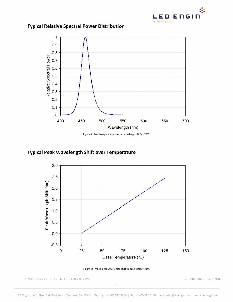
Typical Relative Spectral Power Distribution
Figure 5: Relative spectral power vs. wavelength @ TC = 25°C.
Typical Peak Wavelength Shift over Temperature
Figure 6: Typical peak wavelength shift vs. case temperature.

10
LED Engin | 651 River Oaks Parkway | San Jose, CA 95134 USA | ph +1 408 922 7200 | fax +1 408 922 0158 | em [email protected] | www.ledengin.com
COPYRIGHT © 2018 LED ENGIN. ALL RIGHTS RESERVED. LZ1-00DB00 (6.0 – 05/11/18)
0
0.2
0.4
0.6
0.8
1
1.2
1.4
0 200 400 600 800 1000 1200 1400 1600
IF - Forward Current (mA)
No
rma
lize
d R
ad
iant
Flu
x
0
0.2
0.4
0.6
0.8
1
1.2
0 25 50 75 100 125 150
Case Temperature (ºC)
Norm
aliz
ed R
adin
at F
lux
Typical Normalized Radiant Flux
Figure 7: Typical normalized radiant flux vs. forward current @ TC = 25°C.
Typical Normalized Radiant Flux over Temperature
Figure 8: Typical normalized radiant flux vs. case temperature.

11
LED Engin | 651 River Oaks Parkway | San Jose, CA 95134 USA | ph +1 408 922 7200 | fax +1 408 922 0158 | em [email protected] | www.ledengin.com
COPYRIGHT © 2018 LED ENGIN. ALL RIGHTS RESERVED. LZ1-00DB00 (6.0 – 05/11/18)
0
200
400
600
800
1000
1200
1400
1600
0 25 50 75 100 125 150
Maximum Ambient Temperature (ºC)
I F -
Maxim
um
Curr
ent
(mA
)
RΘJ-A = 9°C/W
RΘJ-A = 13°C/W
RΘJ-A = 17°C/W
0
200
400
600
800
1000
1200
1400
1600
2.8 3 3.2 3.4 3.6 3.8 4
VF - Forward Voltage (V)
I F - F
orw
ard
Curr
ent (m
A)
Typical Forward Current Characteristics
Figure 9: Typical forward current vs. forward voltage @ TC = 25°C.
Current Derating
Figure 10: Maximum forward current vs. ambient temperature based on TJ(MAX) = 150°C. Notes for Figure 10:
1. RΘJ-C [Junction to Case Thermal Resistance] for the LZ1-00DB00 is typically 4.2°C/W. 2. RΘJ-A [Junction to Ambient Thermal Resistance] = RΘJ-C + RΘC-A [Case to Ambient Thermal Resistance].

12
LED Engin | 651 River Oaks Parkway | San Jose, CA 95134 USA | ph +1 408 922 7200 | fax +1 408 922 0158 | em [email protected] | www.ledengin.com
COPYRIGHT © 2018 LED ENGIN. ALL RIGHTS RESERVED. LZ1-00DB00 (6.0 – 05/11/18)
Emitter Tape and Reel Specifications (mm)
Figure 11: Emitter carrier tape specifications (mm).
Figure 12: Emitter reel specifications (mm). Notes: 1. Small reel quantity: up to 500 emitters 2. Large reel quantity: 501-2500 emitters. 3. Single flux bin and single wavelength bin per reel. 4. Previous version of the emitter (p/n: LZ1-00DB00-0000) has different emitter position in the Tape and Reel. Please refer to PCN 54-2 for more details.
Ø 178mm (SMALL REEL) Ø 330mm (LARGE REEL)
13
LED Engin | 651 River Oaks Parkway | San Jose, CA 95134 USA | ph +1 408 922 7200 | fax +1 408 922 0158 | em [email protected] | www.ledengin.com
COPYRIGHT © 2018 LED ENGIN. ALL RIGHTS RESERVED. LZ1-00DB00 (6.0 – 05/11/18)
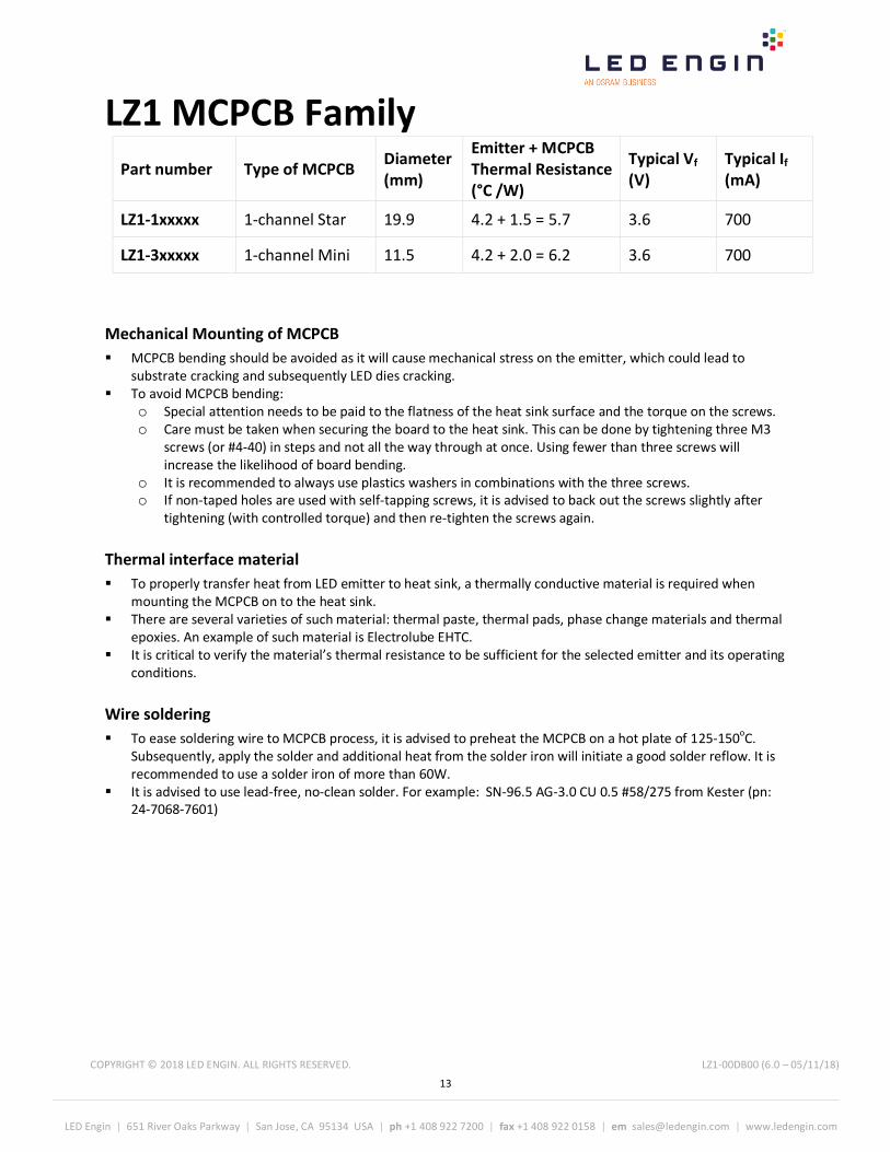
LZ1 MCPCB Family Part number Type of MCPCB
Diameter (mm)
Emitter + MCPCB Thermal Resistance (°C /W)
Typical Vf (V)
Typical If (mA)
LZ1-1xxxxx 1-channel Star 19.9 4.2 + 1.5 = 5.7 3.6 700
LZ1-3xxxxx 1-channel Mini 11.5 4.2 + 2.0 = 6.2 3.6 700
Mechanical Mounting of MCPCB
MCPCB bending should be avoided as it will cause mechanical stress on the emitter, which could lead to substrate cracking and subsequently LED dies cracking.
To avoid MCPCB bending: o Special attention needs to be paid to the flatness of the heat sink surface and the torque on the screws. o Care must be taken when securing the board to the heat sink. This can be done by tightening three M3
screws (or #4-40) in steps and not all the way through at once. Using fewer than three screws will increase the likelihood of board bending.
o It is recommended to always use plastics washers in combinations with the three screws. o If non-taped holes are used with self-tapping screws, it is advised to back out the screws slightly after
tightening (with controlled torque) and then re-tighten the screws again.
Thermal interface material
To properly transfer heat from LED emitter to heat sink, a thermally conductive material is required when mounting the MCPCB on to the heat sink.
There are several varieties of such material: thermal paste, thermal pads, phase change materials and thermal epoxies. An example of such material is Electrolube EHTC.
It is critical to verify the material’s thermal resistance to be sufficient for the selected emitter and its operating conditions.
Wire soldering
To ease soldering wire to MCPCB process, it is advised to preheat the MCPCB on a hot plate of 125-150oC. Subsequently, apply the solder and additional heat from the solder iron will initiate a good solder reflow. It is recommended to use a solder iron of more than 60W.
It is advised to use lead-free, no-clean solder. For example: SN-96.5 AG-3.0 CU 0.5 #58/275 from Kester (pn: 24-7068-7601)

14
LED Engin | 651 River Oaks Parkway | San Jose, CA 95134 USA | ph +1 408 922 7200 | fax +1 408 922 0158 | em [email protected] | www.ledengin.com
COPYRIGHT © 2018 LED ENGIN. ALL RIGHTS RESERVED. LZ1-00DB00 (6.0 – 05/11/18)
LZ1-1xxxxx 1 channel, Standard Star MCPCB (1x1) Dimensions (mm)
Notes:
Unless otherwise noted, the tolerance = ± 0.2 mm.
Slots in MCPCB are for M3 or #4-40 mounting screws.
LED Engin recommends plastic washers to electrically insulate screws from solder pads and electrical traces.
LED Engin recommends using thermal interface material when attaching the MCPCB to a heat sink.
The thermal resistance of the MCPCB is: RΘC-B 1.5°C/W
Previous version of the emitter (p/n: LZ1-10DB00-0000) has different marking: -,+,+,- for pin 1,2,3,4. Please refer to PCN 55 for more details.
Components used MCPCB: HT04503 (Bergquist) ESD/TVS Diode: BZT52C5V1LP-7 (Diodes, Inc., for 1 LED die) VBUS05L1-DD1 (Vishay Semiconductors, for 1 LED die)
Pad layout
Ch. MCPCB Pad
String/die Function
1 1,2,3
1/A Cathode -
4,5,6 Anode +

15
LED Engin | 651 River Oaks Parkway | San Jose, CA 95134 USA | ph +1 408 922 7200 | fax +1 408 922 0158 | em [email protected] | www.ledengin.com
COPYRIGHT © 2018 LED ENGIN. ALL RIGHTS RESERVED. LZ1-00DB00 (6.0 – 05/11/18)
LZ1-3xxxxx 1 channel, Mini Round MCPCB (1x1) Dimensions (mm)
Notes:
Unless otherwise noted, the tolerance = ± 0.20 mm.
LED Engin recommends using thermal interface material when attaching the MCPCB to a heat sink.
The thermal resistance of the MCPCB is: RΘC-B 2.0°C/W
Previous version of the emitter (p/n: LZ1-30DB00-0000) has different marking: -,+,+,- for pin 1,2,3,4. Please refer to PCN 55 for more details.
Components used MCPCB: HT04503 (Bergquist) ESD/TVS Diode: BZT52C5V1LP-7 (Diodes, Inc., for 1 LED die) VBUS05L1-DD1 (Vishay Semiconductors, for 1 LED die)
Pad layout
Ch. MCPCB Pad
String/die Function
1 1
1/A Anode +
2 Cathode -
16
LED Engin | 651 River Oaks Parkway | San Jose, CA 95134 USA | ph +1 408 922 7200 | fax +1 408 922 0158 | em [email protected] | www.ledengin.com
COPYRIGHT © 2018 LED ENGIN. ALL RIGHTS RESERVED. LZ1-00DB00 (6.0 – 05/11/18)
About LED Engin LED Engin, an OSRAM business based in California’s Silicon Valley, develops, manufactures, and sells advanced LED emitters, optics and light engines to create uncompromised lighting experiences for a wide range of entertainment, architectural, general lighting and specialty applications. LuxiGenTM multi-die emitter and secondary lens combinations reliably deliver industry-leading flux density, upwards of 5000 quality lumens to a target, in a wide spectrum of colors including whites, tunable whites, multi-color and UV LEDs in a unique patented compact ceramic package. Our LuxiTuneTM series of tunable white lighting modules leverage our LuxiGen emitters and lenses to deliver quality, control, freedom and high density tunable white light solutions for a broad range of new recessed and downlighting applications. The small size, yet remarkably powerful beam output and superior in-source color mixing, allows for a previously unobtainable freedom of design wherever high-flux density, directional light is required. LED Engin is committed to providing products that conserve natural resources and reduce greenhouse emissions; and reserves the right to make changes to improve performance without notice. For more information, please contact [email protected] or +1 408 922-7200.