Embed Size (px)
Citation preview

High Bit Rate Optical Data Bus Technologiesfor Advanced Wireless Handheld Devices
Louay EldadaCTO, VP Engineering
DuPont Photonics Technologies
[email protected]://www.photonics.dupont.com

2DuPont Proprietary
Forms of Energy Used in Data Links
• Electric current (Twisted Pair or Coax)
• Audible sounds (Dial-up)
• Infrared (Fiber Optics)
• Radio frequency (RF)
• Omni-directional electromagnetic waves
• Directional electromagnetic waves− Point-to-point satellite channel− Limited broadcast (spot beam)− Microwave− Laser beam

3DuPont Proprietary
Electrical Interconnects Optical InterconnectsEnergy Form Electrical Current (AC, travels further than DC) Light
Typical Modulation Phase Shift Modulation Amplitude Modulation
Wiring / Splicing Easy Relatively difficultField Data All distances Mainly long distances
Encoding Negative/Positive Voltage encodes signal High/Low Voltage encodes signalMultiplexing TDM, FDM TDM, WDM
Network Centricity Voice-centric Data-centric
Transmission Medium Copper Wire (Twisted Pair [TWP], Coax) Silica Fiber (SF), POF, Planar Polymer
Dimensions TWP: 7.4mm, Coax: 1.9/6.4/7.4mm inner/outer/jacket SF: 8/125/245/2000µm core/clad/jacket/sheathCapacity (Max Bandwidth) TWP: 10/100Mbps 3km/100m, Coax: 300Mbps 100km 25-100 Tbps (varies with fiber type)
Max Distance Before Amplification 5 km between repeaters 40 km (Std), Continuous in-fiber (Raman)Max Distance Before Regeneration 5 km between repeaters 500 km (Std), 3000 km (Raman)
Security Low (can be tapped inductively) High (cannot be tapped non-disruptively)
Signal Transmission Speed High (2/3 speed of light in vacuum) High (2/3 speed of light in vacuum)
Signal Quality Wire R, C, L, & Mag. or Elec. interference distort signals Fiber dispersion smears signals
Cost High Low
Weight High (1000 1-km TWP: 8000 kg) Low (2 1-km fibers: 100 kg)
Upgradability Requires Digging Does Not Require Digging (Multiplexing)Energy Dissipation Electrical energy dissipates with distance Optical energy is absorbed with distance
Flexibility Low High
Signal Processing Speed Low High (All-Optical)
Bending Radius Large Small
Efficiency Low High
Immunity to Noise Low High
Ability to Withstand Pulling Low High
Distance Short Long
Green: SuperiorBlue: Inferior
Electrical vs. Optical Interconnects

4DuPont Proprietary
Optical InterconnectsKey Advantages over Electrical Interconnects
• Immunity to EMI• High bandwidth• Low signal attenuation• Long reach• Easy thermal management• Negligible dispersion• Future scalability beyond 1Tbps• Low media cost• Small size and light weight• Easy cable management• Robustness• Low latency• Low power consumption• High port density

5DuPont Proprietary
Optical Interconnects vs. CopperHigh Speed
Long Distance
ESEC
Low SpeedShort Distance
Transition from electrical to optical interconnects:• Increases bandwitdh-length product• Increases interconnect density• Decreases cost per bit for board-to-board & beyond
0.01 0.1 1 10 100 1000Data Rate (Gb/s)
100
101
102
103
104
105
Den
sity
(Int
erco
nnec
ts/m
m2 )
Diffraction Limit
Optical Free Space
Optical Fiber
Electrical Loss Limit
Coax

6DuPont Proprietary
Optical InterconnectsGlass Fiber vs. Polymer Interconnects
Glass Fiber InterconnectsPros:• Widely available technology• Optical loss (0.00002-0.0005 dB/cm)• 50 m @ 20 GbpsCons:• Costly• Labor intensive• Bulky• Point-to-point only (no passives)
Planar Polymer InterconnectsPros:• Dense, compact integration• Cost efficient ($1/Gbps 10-50m)• 10 m @ 20 Gbps• Passive structures possible• High flexibility• Mechanical resiliency• Embedded in/on board, compatible
with lamination pressure & 260°C Pb-free wave soldering
Cons:• Optical loss (0.0005-0.05 dB/cm)• Availability of best polymers• Stability of some polymers

7DuPont Proprietary
Organics as Optical Interconnects
PCB & CMOS Compatibility:• Conform to topography• Planarization easy• Can be fabricated in/on boards, and on finished CMOS chips• Minimal temperature excursion (process temperature < 100°C)• Low temperature dissipation for dynamic functions
Manufacturability:• Rapid processes (stamping, etc.)• Low cost• Ready now• Compatible with high temperatures (up to 400°C)
Adaptability:• All elemental functions achievable• Widely tunable refractive index contrast• Post-fab trimming/rework possible• 3D routing possible (2-photon polymerization, etc.)

8DuPont Proprietary
Organics in Packaging
Organic Coatings:• Broadly used for chip passivation, planarization, anti-reflection
coatings, etc.
Organic Adhesives:• Broadly used for pigtailing of optical chips, die attach, surface
mount, flip-chip underfills, etc.
Organic Sealants:• Provide low cost semi-hermetic sealing of packages (at lid,
ferrule, etc.) for moderate-length lifetimes (5-10 years)
Organic Encapsulants:• Ultra-low cost packaging using glob-top coating, “dam and fill”
encapsulants, etc.
Plastic Packages:• Very low cost packages/cases/enclosures/boxes for non-hermetic
components

9DuPont Proprietary
Polymer Optical InterconnectsOEMs Active in the Field
• Agilent
• Fujitsu
• IBM
• Intel
• LG
• Motorola
• Samsung
• Sun Microsystems
• etc.

10DuPont Proprietary
OpticalPolymers
Global MaterialProduction Effort
11DuPont Proprietary
Optical Polymer Requirements
1. Low absorption loss2. Low wavelength dependent loss (WDL)3. Low polarization dependent loss (PDL)4. Low polarization mode dispersion (PMD)5. Low chromatic dispersion (CD)6. Low birefringence7. Low stress8. Low fiber pigtail loss9. Closeness to refractive index of silica fiber10. Stability of refractive index11. Variable refractive index difference (∆n)12. Variable refractive index profile13. Low refractive index dispersion (dn/dλ)14. Large T/O coefficient (dn/dT)15. Linearity of refractive index with temperature16. Optimal thermal conductivity17. Thermal stability18. No phase transition in operating range19. Stability with humidity20. Hydrophobicity21. Stability with optical power22. Adhesion (to substrates, self, electrodes)23. Compatibility with electrode patterning24. Low reactivity to acids, bases, solvents25. Stability with oxygen
26. Isotropy27. Homogeneity28. Low level of impurities29. Optimal molecular weight distribution30. Optimal viscosity31. Low volatility32. Optimal photosensitivity33. Optimal cure speed34. Full curability35. Thermoset material36. High crosslink density37. Low shrinkage38. Optimal free volume39. Contrast in patterning40. Optimal surface energy41. Processability for high film quality42. Process latitude in patterning43. Patternability with low scattering loss44. Machinability (cleaving, dicing, polishing)45. Mechanical robustness46. Flexibility47. Stability of mechanical integrity48. Volume manufacturability49. Manufacturability with repeatable properties50. Long shelf life
The Top 50 List
Not an easy task –After 25 years of molecular nanoengineering,
DuPont optical polymers meet all 50 requirements

12DuPont Proprietary
Hyper-branched FluoropolymersNanoengineered for Communication Applications
Properties:
• Low Absorption at 800-1600 nm– Halogenation
• High Stability– Molecular design
• Low Birefringence and PDL– Isotropic & homogeneous
• Low Shrinkage– High MW
• Fast Curing– One end pre-fixed
• High Crosslink Density– One end pre-fixed
• Low Volatility– High MW
• Controlled Viscosity– MW & molecular structure
• High dn/dT for Thermo-optics– High free volume & low Tg
Rf I Rf
Rf I
Rf
Rf
Rf I Rf
Rf
Rf
Rf I Rf
Rf Rf
Rf Rf
Rf I Rf I Rf
Rf
I Rf
Rf
I
Rf
Rf
Rf I Rf
Rf
I Rf
RfRf
Rf
Rf I Rf I Rf
Rf Rf
Rf Rf
Rf Rf
Rf Rf

13DuPont Proprietary
Cycle Time Minutes/wafer
Propagation Loss 0.11 dB/cm (sm wg)
Polarization Effects Birefringence = 10-6
PMD = 0.01 ps (1 cm sm wg) PDL = 0.01 dB (1 cm sm wg)
T/O Coefficient dn/dT = -3.2x10⁻⁴
Index Contrast ∆n = 0-30%
Reliability Proven
Functions Static & Dynamic in Polymer Active by Hybrid Integration
Propagation Loss = 0.11 dB/cmPigtail Loss = 0.14 dB per side
Chip Length [mm]0 10 20 30
Inse
rtion
Los
s [d
B]
0.0
0.2
0.4
0.6
0.8
1.0
dn/dT = -3.2x10⁻⁴
Temperature [ C]20 30 40 50 60
Ref
ract
ive
Inde
x (n
)
1.345
1.350
1.355
°
DuPont Polymer PLCsKey Properties at 1550 nm
WDL < 0.05 dB
Wavelength (nm)1500 1520 1540 1560 1580
Inse
rtion
Los
s (d
B)
0.0
0.2
0.4
0.6
0.8
1.0
Low Insertion Loss
Low Power Consumption
Low Wavelength Dependence
32x lower than silica
14DuPont Proprietary
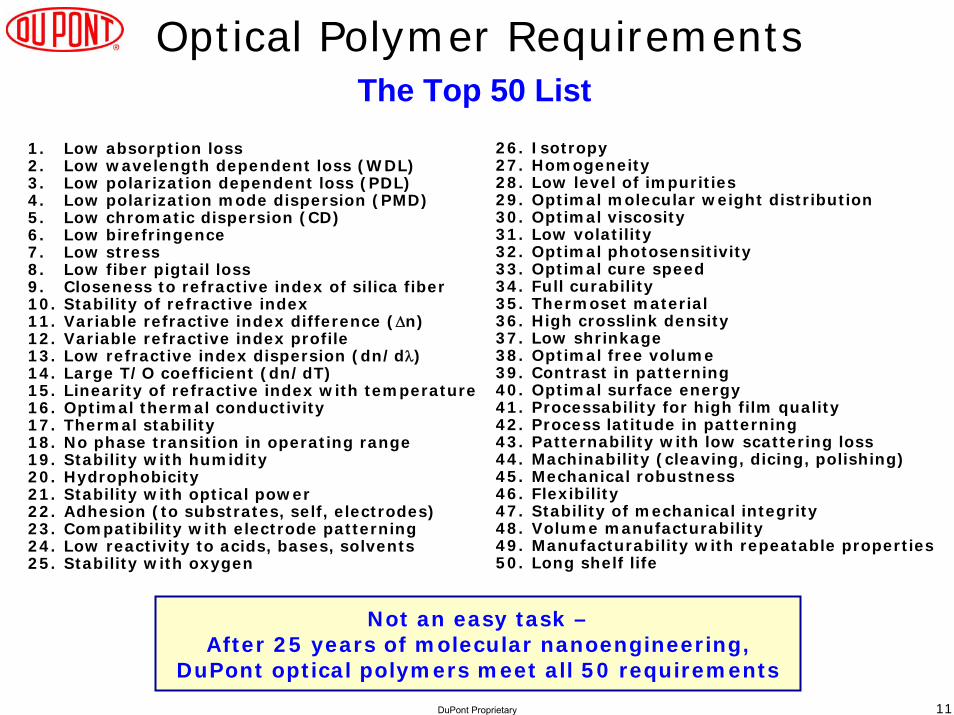
• Absorption loss, minimized by:− Halogenation• Scattering loss, minimized by:− Homogeneous medium− Minimal roughness− Low intrinsic stresses− Graded index− Large mode field diameter
• Radiation loss, minimized by:− Large radii of curvature− Adiabatic modal transitions• Mode overlap loss (with fiber), minimized by:− Mode matching− Optimized alignment• Fresnel reflection loss, minimized by:− Index difference minimization at interfaces
Optical Loss in WaveguidesThe 5 types of loss & how to minimize them
CH BondsCD BondsCF BondsCCl BondsPMMADuPont Polymer

15DuPont Proprietary
DuPont PolymersAbsorption Loss Spectra
0.8 0.9 1.0 1.1 1.2 1.3 1.4 1.5 1.6 1.7
Wavelength (µm)
0.01
0.10
1.00
Loss
(dB
/cm
)
80% HalogenationAt λ=800-900 nm: <0.01 dB/cmAt λ=1290-1330 nm: 0.03 dB/cmAt λ=1500-1600 nm: 0.09 dB/cm
Teflon® AF (100% Halogenation)At λ=800-1600 nm: <0.001 dB/cm(At λ=800-900 nm: 0.0005 dB/cm)

16DuPont Proprietary
Refractive Index Contrast
∆n Standard Medium Med. High High Very High Ultra High Highest
∆n value 0.0075 0.01125 0.015
1%
4.5x4.5 µm2
0.56 dB
Bend Radius*** 15 mm 6 mm 4 mm 2 mm 0.5 mm 0.1 mm 0.01 mm
0.0225 0.045 0.45
∆n/n 0.5% 0.75% 1.5% 3%
0.15
10%
1x1 µm2
8.0 dB
30%
Core Size* 7x7 µm2 6x6 µm2 3x3 µm2 2x2 µm2 0.5x0.5 µm2
Coupling Loss** 0.0077 dB 0.23 dB 1.6 dB 4.2 dB 9.6 dB
Chip Size****
* Largest core size for square-cross-section single-mode burried channel waveguide** Lowest possible coupling loss to Corning SMF28 fiber for both sides of chip
*** Smallest radius of curvature for negligible bend radiation loss**** Relative dimensions
• Optical polymer refractive indices span the range from 1.3 to 1.7• Refractive index contrast is the core/cladding index difference (∆n)• Refractive index contrast is controlled by material composition• Refractive index contrast continuously tunable between 0 and 30%
n1 n2
n1<n<n2
n
Numerical Aperture Control

17DuPont Proprietary
Polymer Optical Circuit Fabrication• Form monomer film, expose, develop• Form oligomer/solvent film, bake, expose, develop• Reactive ion etching• Hot embossing• Soft embossing• Compression molding• Injection molding• Casting• Stamping
• Films formed by spin coating, spray coating, slot coating, doctor blading (tape casting), or dipping
• UV exposure performed with mask and UV lamp or by laser direct writing• Material can be negative tone or positive tone
PhotomaskPhotosensitive Material
UndercladSubstrate
UV
Core Exposure Development Overclad

18DuPont Proprietary
Reel-to-reel Processing is used for rapid cost-effective mass production of long, flexible, planar photonic circuits
Laser direct writingof waveguides on chips, multi-chip modules (MCM’s), boards, and backplanes allows to interconnect transmit/ receive elements regardless of surface topography
Unexposed waveguideMaterial on 1000’ roll
Chrome on fused silicaphotomask
Buffer layers laminated to core layer
UV exposure lamp
Finished waveguides are diced, ready for fiber coupling
DuPont Polyguide®
StampingUV Exposure & Lamination
Polymer Optical InterconnectsFabrication Approaches

19DuPont Proprietary
Waveguide Photopolymer
Core
Lower Polyimide Layer
Upper Cladding Polymer
Upper Polyimide Layer
Lower Cladding Polymer
Polymer Optical InterconnectsDuPont Optoflex Stack

20DuPont Proprietary
• Typical core dimensions:
– Width at top: 45 µm
– Width at bottom: 55 µm
– Height: 55 µm
• Typical indices of refraction at 850 nm: nclad=1.48-1.52 ncore=1.52-1.56
• Typical index of refraction difference between core and clad: ∆n=0.008-0.08
• Typical ∆n/n=0.5-5%
Polymer Optical InterconnectsDimensions & Refractive Indices

21DuPont Proprietary
Polymer waveguide excited by multimode fiber
Polymer Optical InterconnectsNear-Field Output Intensity Pattern

22DuPont Proprietary
Plastic Optical FiberComparison with Glass Optical Fiber
Glass Optical Fiber
● Small Core: Up to 62.5µm● Small Connectorization
Tolerance● Polishing● Brittle & Fragile● Low NA
POFPolymer CorePolymer Clad
GOFSilica CoreSilica Clad
Plastic Optical Fiber
● Large Core: Up to 1mm● Large Connectorization
Tolerance● Polishing-Free● Flexible & durable● High NA

23DuPont Proprietary
Plastic Optical Fiber
• High bandwidth• High flexibility• High durability• Easy handling and processing• Light weight• EMI immunity• Low cost components• Low attenuation
Advantages over Copper Based Interconnects
24DuPont Proprietary
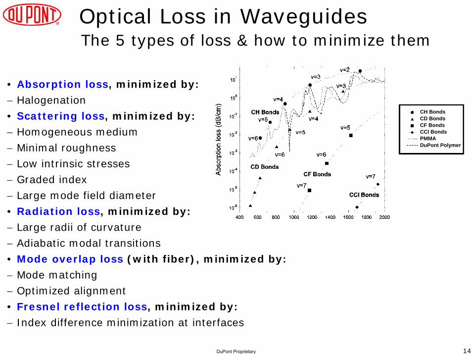
Reliability of Organic MaterialsCan Organics Be Reliable in Demanding Environments?
DuPont organic materials are used in computers, cell phones, display panels, PDAs, video camcorders, and digital cameras, making these products smaller and more durable, while allowing them to do more, faster, better, and at lower cost.In addition, they are used in:

25DuPont Proprietary
Telcordia Qualification
0
1
2
3
4
5
6
7
8
9
10
-0.5 -0.4 -0.3 -0.2 -0.1 0.0 0.1 0.2 0.3 0.4 0.5
Change in Insertion Loss (dB)
Nu
mb
er
of
Ch
an
ne
ls
1528 nm1550 nm1565 nm
DuPont’s polymer-based photonic components passedTelcordia 1209/1221 qualification with a large margin
Narrow data distribution around 0 dB IL changeChanges on order of measurement error
Telcordia TestsGR-1209-CORE/GR-1221-CORE
High Temperature Storage(85°C, 2000 hours)
Lifetest(70°C, 2000 hours, in-situ operation & test)
Temperature-Humidity Aging(85°C/85%RH, 336 hours)
Temperature Cycling(-40°C to 85°C, 100 cycles)
Thermal Shock(0°C to 100°C, 15 cycles)
Vibration(20-2000 Hz, 3 axes, 4 cycles/axis)
Mechanical Shock(500 G, 6 directions, 5 times/direction)
Cable Retention(3.4 lb load, 1 minute)
Fiber Side Pull(0.5 lb load, 90° angle)

26DuPont Proprietary
Reliability of Polymers and DevicesHighly Accelerated Stress Tests (HAST)
Lifetime > 20 years at maximumoperating temperature of 150°C
-0.5
-0.4
-0.3
-0.2
-0.1
0
0.1
0.2
0.3
0.4
0.5
0 1000 2000 3000 4000 5000 6000
Duration (hours)Tr
ansm
issi
on V
aria
tion
(dB
/cm
)
20-year degradation< 0.08 dB/cm at 17 dBm input power< 0.02 dB/cm at 10 dBm input power
0 500 1000 1500 2000 2500 3000 3500 4000 4500 5000
Time (hours)
-0.5
-0.4
-0.3
-0.2
-0.1
0.0
0.1
0.2
0.3
0.4
0.5
Inse
rtio
n Lo
ss V
aria
tion
(dB
)
5000 Hours, 175°C
Device 1Device 2Device 3Device 4
175°C, 5000 hours10-cm-long waveguides
(1550 nm)
32 dBm (1.5 W), 6000 hours(1550 nm)
Stability with High Temperature
Stability with High Optical Power
Polymer lifetime well over lifetime of other components in system
Optical intensity in polymer waveguide = 2.5x10¹⁰ W/m2
→ 100x optical intensity on the surface of the Sun

27DuPont Proprietary
Interconnects
Chip to ChipChip to Chip1 1 –– 50 cm50 cm
Board to BoardBoard to Board50 50 –– 100 cm100 cm
1 to 100 m1 to 100 m
Rack to Rack to RackRack
0.1 0.1 –– 80 km80 km
Metro &Metro &Long HaulLong Haul
Decreasing DistancesDecreasing Distances→→
BillionsBillions
MillionsMillions
ThousandsThousands
Vo
lum
es
Vo
lum
es
OpticalOptical CopperCopper
Drive optical to high volumes and low costs
$100’s / channel ¢1’s / pin
1 Billion Cell PhonesOptical Data Bus
~$2.50/chTAM ~$5B
5000 WAN NodesRouting Subsystem
$250/chTAM ~$50M
Cell vs. WAN: 2 orders of magnitude lower cost per channelYet 2 orders of magnitude larger total addressable market
28DuPont Proprietary
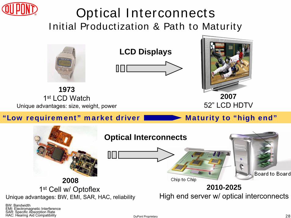
Optical InterconnectsInitial Productization & Path to Maturity
19731st LCD Watch
Unique advantages: size, weight, power
LCD Displays
200752” LCD HDTV
20081st Cell w/ Optoflex
Unique advantages: BW, EMI, SAR, HAC, reliability
Optical Interconnects
BW: BandwidthEMI: Electromagnetic InterferenceSAR: Specific Absorption RateHAC: Hearing Aid Compatibility
2010-2025High end server w/ optical interconnects
“Low requirement” market driver Maturity to “high end”

29DuPont Proprietary
Optical InterconnectsHigh End Needs Met over Time
• Bandwidth
• Reliability
• Design Tools
• Standardization of sub-components
• Manufacturing/Test Infrastructure
• Cost per element

30DuPont Proprietary
Applications requiring optical solutions are typically associated with:• High end• High cost• High data-rate
Handheld communication devices require low cost, are relatively low end (vs. supercomputer), and have moderate data-raterequirements, but they have high volume that can drive innovations and standards in optical interconnects, and will seethe first commercial adoption of these technologies
Precedence – cell phones have driven innovations in:• High density interconnects (HDI) technology used in PCBs to
reduce size and weight, and enhance electrical performance• Power efficient chip technology, including low-power HDMI
(High Definition Multimedia Interface)
Handheld Communication DevicesLeading the Way in Innovation

31DuPont Proprietary
Handheld devices have rapidly increasing:Resolution of displaysResolution of camerasSpeed of CPUs / GPUsStorage capacity
Resulting in:Higher data rates within these devices and to the outside world
Therefore requiring:Continuous innovation in data bus technologies
Copper interconnects are reaching their limits in high-end handhelds:SmartphonesPersonal digital assistants (PDA)Portable multimedia players (PMP, e.g., iPod)Wireless handheld game consoles (e.g., PSP)
Optical InterconnectsDrivers in Handhelds
32DuPont Proprietary
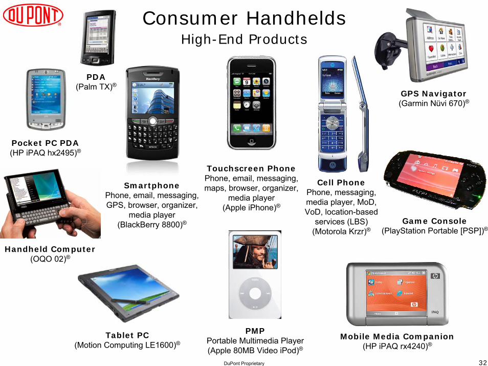
Consumer HandheldsHigh-End Products
Handheld Computer(OQO 02)®
Mobile Media Companion(HP iPAQ rx4240)®
Pocket PC PDA(HP iPAQ hx2495)®
Tablet PC(Motion Computing LE1600)®
GPS Navigator(Garmin Nüvi 670)®
SmartphonePhone, email, messaging, GPS, browser, organizer,
media player(BlackBerry 8800)®
Cell PhonePhone, messaging, media player, MoD,VoD, location-based
services (LBS)(Motorola Krzr)®
PMPPortable Multimedia Player(Apple 80MB Video iPod)®
Game Console(PlayStation Portable [PSP])®
Touchscreen PhonePhone, email, messaging, maps, browser, organizer,
media player(Apple iPhone)®
PDA(Palm TX)®

33DuPont Proprietary
Bit rates needed in data buses of advanced handhelds:up to 700 Mbps in 20071.25 Gbps in 20085 Gbps in 2012
Electrical interconnects are bottleneck, high bit rate links formed with dense parallel copper lines have:
Electromagnetic interference (EMI) issues cost significant time & resources, delay time to marketIncreasingly complex electrical flex interconnects
6+ layers air-gap polyimide flex50+ pin fine-pitch connectors
Thermal dissipation issues due to proximity of highest power consumption components (e.g., CPU & GPU) because of limited datarate of long electrical interconnects
EMI complicates compliance with regulations including:Specific Absorption Rate (SAR)Hearing Aid Compatibility (HAC)Out of band frequency interference
Optical Interconnects in Handhelds Technical Drivers

34DuPont Proprietary
Optical interconnects in handheld devices can:Bus high bandwidth signals through a simple serial interfaceEliminate the data bus contribution to EMI and SAR
Passive and active optical interconnect technologies that enable high-performance optical data buses in handhelds are mature, including:
VCSELsHigh speed detectorsElectronic drivers (TIA, etc.)Polymer optical interconnects (flex strips & POF)
Optical Interconnects in Handhelds

35DuPont Proprietary
Emerging applications requiring high-bit-rate data buses in handheld devices include:
Live gaming – latency not tolerated in real-time battles where reflexes matter
►Shoot’em ups: Halo, Counter-Strike►Quest games: World of Warcraft
Portable global positioning system (GPS)Capturing and displaying high-resolution imagesCapturing & playing high-frame-rate high-resolution video
Optical InterconnectsApplication Drivers in Handhelds

36DuPont Proprietary
Halo Wars® is a real time strategy game; will be released in Fall 2007
Counter-Strike® is a team-based, tactical shooter game; puts a team of counter-terrorists
against a team of terroristsWorld of Warcraft® is a massive multiplayer online role-playing game
Optical Interconnects in HandheldsApplication: Live Gaming
Latency not tolerated in real-time games
where reflexes matter

37DuPont Proprietary
Optical InterconnectsUse in Handhelds
3D Video EyewearVirtual big screen viewing of3D HD rich media content
(my vu)®
Big Screen HDTV1920x1080 Resolution (2.07 Megapixels)
(SONY)®
Desktop PC(Dell)®
HD NotebooksWUXGA (Wide Ultra Extended Graphics array)
1920x1200 Resolution (2.30 Megapixels)(Dell)®
High bandwidth links for handhelds that can benefit from optical interconnects►Internal to Handheld Device:
Hi Res Camera (CMOS sensors) to CPU & StorageGPU to Hi Res Display (LCD cells)CPU to GPUCore to Core
►External to Handheld Device:Handheld to HDTV / HD monitorHandheld to Storage Device (e.g., PC Hard Drive)Handheld to HD Eyewear

38DuPont Proprietary
Plastic Optical FiberExisting Consumer Applications
POF-Based Car Network POF-Based Home Network
POF is ideal medium for short range high bandwidth links, as needed between handheld devices and external equipment. POF was invented by DuPont in 1968.
Mitsubishi Rayon EskaTM POF is based on DuPont Teflon® AFTeflon® AF is 4,5-difluoro-2,2-bis(trifluoromethyl)-1,3-dioxole

39DuPont Proprietary
Interconnects in HandheldsCompeting Technologies
EMI / SARReduction
MechanicalReliability
Novel DesignEnabler
Power Consumption Cost
Copper FlexParallel I/F
Micro CoaxCable Parallel I/F
Copper FlexDifferential Serial I/F
CoaxDifferential I/F
OpticalSerial I/F
Mot
orol
a (p
artia
lly)

40DuPont Proprietary
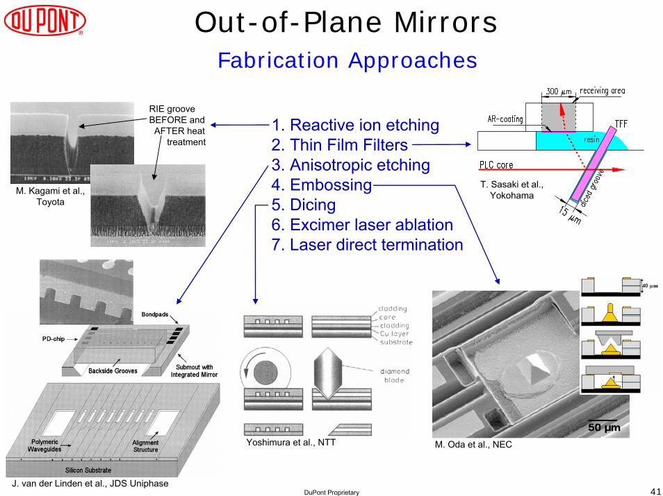
Requirements for 45° out-of-plane mirrors:• High reflectivity (>80%)• Precise mirror plane position (±2-3 µm)• Possibility of up and down routing• Symmetry of in and out coupling• Full integration with waveguides• Robust and cost-effective manufacturing process• Possibility of multilayer 3D structures
Multilayer 3D structures
45° Out-of-Plane Mirrors
Optical‘Via’
Fujitsu
41DuPont Proprietary
Out-of-Plane Mirrors
J. van der Linden et al., JDS Uniphase
T. Sasaki et al.,Yokohama
M. Oda et al., NEC
RIE groove BEFORE and AFTER heat
treatment
M. Kagami et al.,Toyota
1. Reactive ion etching2. Thin Film Filters 3. Anisotropic etching4. Embossing5. Dicing6. Excimer laser ablation7. Laser direct termination
Yoshimura et al., NTT
Fabrication Approaches

42DuPont Proprietary
45° angle termination of waveguides allows 90° out-of-plane bending of the light for the coupling of light from VCSEL’s into waveguides or from waveguides into detectors
45° angle termination can be achieved during the waveguide fabrication with laser direct writing or through post-processing
using Excimer laser ablation
45° Angle TerminationPolymer Optical Interconnects

43DuPont Proprietary
Interconnects on p-i-n detectors
Interconnect on high-speed receiver
Interconnects on VCSEL Array
Polymer Optical Interconnects

44DuPont Proprietary
Flexible Interconnect
Strip
MT Connector
Interconnected Transmitter & Receiver Boards
Optical Connectors for Pluggable Interconnects
In-Plane Connections
622 Mbps

45DuPont Proprietary
Indu
stria
l Phy
sici
st, J
une
1999
Intra-Board Interconnects VCSEL-Based Transponder using
DuPont Polymer Optical Interconnects

46DuPont Proprietary
144 Channel Polymer Optical BackplanePolymer Optical Interconnects

47DuPont Proprietary
Communications Technology Roadmap at MIT
The Communications Technology Roadmap is a 3-year (Jan ’06 – Dec ’08) consortium program managed by the MIT Microphotonics Center and lead by industry experts, with the goal of developing a roadmap for the field of microphotonics in areas including telecommunication, datacommunication, computing, imaging and learning, with emphasis on the convergence of electronics and photonics.

48DuPont Proprietary
The CTR consortium has 3 Technology Working Groups (TWGs):
1. Cross-Market Applications:Technical Requirements & Architectural Options
2. CMOS (Si) Platform
3. Integration, Packaging & Interconnection (IPI)
Communications Technology Roadmap at MIT
49DuPont Proprietary
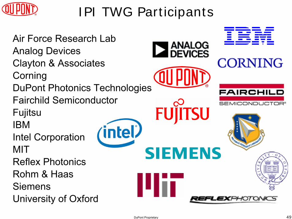
Air Force Research LabAnalog DevicesClayton & AssociatesCorningDuPont Photonics TechnologiesFairchild SemiconductorFujitsuIBMIntel CorporationMITReflex PhotonicsRohm & HaasSiemensUniversity of Oxford
IPI TWG Participants

50DuPont Proprietary
IPI TWG Output
White Papers identifying current technical challenges, future technical requirements & possibly converged integration and packaging strategies for emerging markets, covering 3/5/10 year time horizons. IPI TWG student research project will help answers these questions.
Strategic Roadmap with market-based technical challenges, opportunities and barriers to implement a converged architecture, timeline by which the challenges must be addressed, and impacts if industry cannot meet the roadmaps or convergence opportunities.
Prototype of pluggable optical module addressing some of the needs of an emerging market, developed at MIT ME department with industry guidance.

51DuPont Proprietary
Focal TopicsEmerging Applications Needing Optical Solutions
Applications
Optical interconnects in consumer products White Paper #1High density PWB optical interconnects White Paper #2Optical interconnects between processors in compute applicationsIntegrated optical components for Edge & Access networksLarge-matrix optical cross-connects for Wide Area Networks (WAN)
Optical Solution Examples
Flexible optical bus in flip phones for display & captureHigh-density optical backplanes / optical PWBOE/EO chips integrated in pluggable packagePluggable splitters (access) & tunable filters (metro edge)DWDM & switch matrices in pluggable packages

52DuPont Proprietary
http://mph-roadmap.mit.edu
Participation in IPI TWG
• If interested in participating in the IPI TWG and helping shape the roadmap for Electronic-Photonic Integration and Packaging, contact:Louay Eldada:[email protected] Grzybowski:[email protected]
• Meeting frequency/times:– Teleconference every 6-8 wks(Fridays 11 AM Eastern)– Meetings twice a year at MIT(Spring & Fall)