Embed Size (px)
Citation preview

MMG3011NT1
1RF Device DataFreescale Semiconductor, Inc.
MMG3011NT1
0--6000 MHz, 15 dB15 dBm
InGaP HBT GPA
Heterojunction Bipolar Transistor(InGaP HBT)Broadband High Linearity AmplifierThe MMG3011NT1 is a general purpose amplifier that is internally
input and output matched. It is designed for a broad range of Class A,small--signal, high linearity, general purpose applications. It is suitablefor applications with frequencies from 0 to 6000 MHz such as cellular,PCS, BWA, WLL, PHS, CATV, VHF, UHF, UMTS and general small--signal RF.
Features Frequency: 0 to 6000 MHz P1dB: 15 dBm @ 900 MHz Small--Signal Gain: 15 dB @ 900 MHz Third Order Output Intercept Point: 28 dBm @ 900 MHz Single 5 V Supply Internally Matched to 50 Ohms Cost--effective SOT--89 Surface Mount Plastic Package In Tape and Reel. T1 Suffix = 1,000 Units, 12 mm Tape Width, 7--inch Reel.
SOT--89
Table 1. Typical Performance (1)
Characteristic Symbol900MHz
2140MHz
3500MHz Unit
Small--Signal Gain(S21)
Gp 15 14 12 dB
Input Return Loss(S11)
IRL --18 --25 --25 dB
Output Return Loss(S22)
ORL --25 --18 --17 dB
Power Output @1dBCompression
P1dB 15 13.5 13.5 dBm
Third Order OutputIntercept Point
OIP3 28 26.5 26 dBm
1. VCC = 5 Vdc, TA = 25C, 50 ohm system.
Table 2. Maximum Ratings
Rating Symbol Value Unit
Supply Voltage VCC 6 V
Supply Current ICC 80 mA
RF Input Power Pin 10 dBm
Storage Temperature Range Tstg --65 to +150 C
Junction Temperature TJ 150 C
Table 3. Thermal Characteristics
Characteristic Symbol Value (2) Unit
Thermal Resistance, Junction to CaseCase Temperature 87C, 5 Vdc, 41 mA, no RF applied
RJC 83 C/W
2. Refer to AN1955, Thermal Measurement Methodology of RF Power Amplifiers. Go to http://www.freescale.com/rf.Select Documentation/Application Notes -- AN1955.
LIFETIMEBUY
LASTORDER24
MAY14
LASTSHIP
24MAY15
Document Number: MMG3011NT1Rev. 7, 9/2014
Freescale SemiconductorTechnical Data
Freescale Semiconductor, Inc., 2005--2008, 2012, 2014. All rights reserved.

2RF Device Data
Freescale Semiconductor, Inc.
MMG3011NT1
Table 4. Electrical Characteristics (VCC = 5 Vdc, 900 MHz, TA = 25C, 50 ohm system, in Freescale Application Circuit)
Characteristic Symbol Min Typ Max Unit
Small--Signal Gain (S21) Gp 13.5 15 — dB
Input Return Loss (S11) IRL — --18 — dB
Output Return Loss (S22) ORL — --25 — dB
Power Output @ 1dB Compression P1dB — 15 — dBm
Third Order Output Intercept Point OIP3 — 28 — dBm
Noise Figure NF — 4.6 — dB
Supply Current ICC 32 41 48 mA
Supply Voltage VCC — 5 — V
Table 5. Functional Pin Description
PinNumber Pin Function
1 RFin
2 Ground
3 RFout/DC Supply
Table 6. ESD Protection Characteristics
Test Methodology Class
Human Body Model (per JESD 22--A114) 1A
Machine Model (per EIA/JESD 22--A115) A
Charge Device Model (per JESD 22--C101) IV
Table 7. Moisture Sensitivity Level
Test Methodology Rating Package Peak Temperature Unit
Per JESD 22--A113, IPC/JEDEC J--STD--020 1 260 C
LIFETIMEBUY
LASTORDER24
MAY14
LASTSHIP
24MAY15
Figure 1. Functional Diagram
321
2

MMG3011NT1
3RF Device DataFreescale Semiconductor, Inc.
50 OHM TYPICAL CHARACTERISTICS
5
20
0
TC = 85C
f, FREQUENCY (GHz)
Figure 2. Small--Signal Gain (S21) versusFrequency
15
10
1 2 3 4
Gp,SM
ALL--SIGNAL
GAIN(dB)
25C
--40C
4--40
0
0
S22
f, FREQUENCY (GHz)
Figure 3. Input/Output Return Loss versusFrequency
S11
--10
--20
--30
1 2 3
S11,S22(dB)
15
10
17
5
Pout, OUTPUT POWER (dBm)
Figure 4. Small--Signal Gain versus OutputPower
16
15
14
13
12
7
11
3.532.521.510.510
17
16
15
13
11
f, FREQUENCY (GHz)
Figure 5. P1dB versus Frequency
P1dB,1dB
COMPRESSIONPOINT(dBm
)
14
12
5.40
80
4
VCC, COLLECTOR VOLTAGE (V)
Figure 6. Collector Current versus CollectorVoltage
60
40
10
4.2 5 5.2
I CC,COLLECTORCURRENT(mA)
20
4.4 4.6 4.8 415
30
0
f, FREQUENCY (GHz)
Figure 7. Third Order Output Intercept Pointversus Frequency
27
24
21
18
1 2 3
VCC = 5 Vdc1 MHz Tone Spacing
OIP3,THIRDORDER
OUTPUTINTERCEPTPOINT(dBm
)
11
Gp,SM
ALL--SIGNAL
GAIN(dB)
VCC = 5 Vdc
900 MHz
2140 MHz1960 MHz
2600 MHz
3500 MHz
50
30
9 13
70
VCC = 5 Vdc
VCC = 5 Vdc VCC = 5 Vdc
LIFETIMEBUY
LASTORDER24
MAY14
LASTSHIP
24MAY15

4RF Device Data
Freescale Semiconductor, Inc.
MMG3011NT1
50 OHM TYPICAL CHARACTERISTICS
18
33
4.9
VCC, COLLECTOR VOLTAGE (V)
Figure 8. Third Order Output Intercept Pointversus Collector Voltage
30
27
24
21
OIP3,THIRDORDER
OUTPUTINTERCEPTPOINT(dBm
)
4.95 5 5.15.05
f = 900 MHz1 MHz Tone Spacing
100--40 --20 0 20 40 60 8024
31
T, TEMPERATURE (_C)
Figure 9. Third Order Output Intercept Pointversus Case Temperature
29
28
27
26
OIP3,THIRDORDER
OUTPUTINTERCEPTPOINT(dBm
)
25
Figure 10. Third Order Intermodulation Distortionversus Output Power
Pout, OUTPUT POWER (dBm)
IMD,THIRDORDER
INTERMODULATIONDISTORTION(dBc)
--6 --3 0 3 6--80
--30
--50
--60
--70
--40
150103
105
120
Figure 11. MTTF versus Junction Temperature
104
125 130 135 140 145
TJ, JUNCTION TEMPERATURE (C)
NOTE: The MTTF is calculated with VCC = 5 Vdc, ICC = 41 mA
MTTF(YEARS)
40
8
0
f, FREQUENCY (GHz)
Figure 12. Noise Figure versus Frequency
6
4
2
1 2 3
NF,NOISEFIGURE(dB)
--70
--20
--3
Pout, OUTPUT POWER (dBm)
Figure 13. Single--Carrier W--CDMA AdjacentChannel Power Ratio versus Output Power
--30
--40
--50
--60
960
ACPR,ADJACENTCHANNEL
POWER
RATIO(dBc)
12
30
3
VCC = 5 Vdcf = 900 MHz1 MHz Tone Spacing
129
VCC = 5 Vdc
VCC = 5 Vdc, f = 2140 MHzSingle--Carrier W--CDMA, 3.84 MHz Channel BandwidthInput Signal PAR = 8.5 dB @ 0.01% Probability (CCDF)
VCC = 5 Vdcf = 900 MHz1 MHz Tone Spacing
LIFETIMEBUY
LASTORDER24
MAY14
LASTSHIP
24MAY15
MMG3011NT1
5RF Device DataFreescale Semiconductor, Inc.
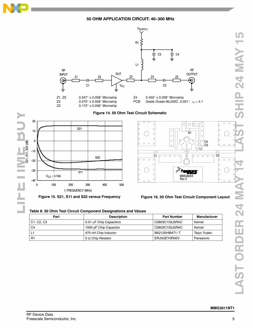
50 OHM APPLICATION CIRCUIT: 40--300 MHz
Figure 14. 50 Ohm Test Circuit Schematic
RFOUTPUT
RFINPUT
VSUPPLY
C3 C4
Z1 Z2
C1
Z5
C2
R1
L1
VCC
Z4Z3DUT
Figure 15. S21, S11 and S22 versus Frequency
--40
20
0
f, FREQUENCY (MHz)
S22
200 300 400 500
10
0
--10
--20
--30
Figure 16. 50 Ohm Test Circuit Component Layout
C1
L1
C2
R1
C4C3
Z1, Z5 0.347 x 0.058 MicrostripZ2 0.575 x 0.058 MicrostripZ3 0.172 x 0.058 Microstrip
Z4 0.403 x 0.058 MicrostripPCB Getek Grade ML200C, 0.031, r = 4.1
S21,S11,S22(dB)
S21
100
MMG30XXRev 2
S11VCC = 5 Vdc
Table 8. 50 Ohm Test Circuit Component Designations and ValuesPart Description Part Number Manufacturer
C1, C2, C3 0.01 F Chip Capacitors C0603C103J5RAC Kemet
C4 1000 pF Chip Capacitor C0603C102J5RAC Kemet
L1 470 nH Chip Inductor BK2125HM471--T Taiyo Yuden
R1 0 Ω Chip Resistor ERJ3GEY0R00V Panasonic
LIFETIMEBUY
LASTORDER24
MAY14
LASTSHIP
24MAY15

6RF Device Data
Freescale Semiconductor, Inc.
MMG3011NT1
50 OHM APPLICATION CIRCUIT: 300--3600 MHz
Figure 17. 50 Ohm Test Circuit Schematic
RFOUTPUT
RFINPUT
VSUPPLY
C3 C4
Z1 Z2
C1
Z5
C2
R1
L1
VCC
Z4Z3DUT
Figure 18. S21, S11 and S22 versus Frequency
--40
20
f, FREQUENCY (MHz)
S22
800
10
0
--10
--20
Figure 19. 50 Ohm Test Circuit Component Layout
C1
L1
C2
R1
C4C3
Z1, Z5 0.347 x 0.058 MicrostripZ2 0.575 x 0.058 MicrostripZ3 0.172 x 0.058 Microstrip
Z4 0.403 x 0.058 MicrostripPCB Getek Grade ML200C, 0.031, r = 4.1
S21,S11,S22(dB)
S21
S11
1300300 1800 2300 2800 3300 3800
MMG30XXRev 2
--30
VCC = 5 Vdc
Table 9. 50 Ohm Test Circuit Component Designations and ValuesPart Description Part Number Manufacturer
C1, C2 150 pF Chip Capacitors C0603C151J5RAC Kemet
C3 0.01 F Chip Capacitor C0603C103J5RAC Kemet
C4 1000 pF Chip Capacitor C0603C102J5RAC Kemet
L1 56 nH Chip Inductor HK160856NJ--T Taiyo Yuden
R1 0 Ω Chip Resistor ERJ3GEY0R00V Panasonic
LIFETIMEBUY
LASTORDER24
MAY14
LASTSHIP
24MAY15

MMG3011NT1
7RF Device DataFreescale Semiconductor, Inc.
50 OHM TYPICAL CHARACTERISTICS
Table 10. Common Emitter S--Parameters (VCC = 5 Vdc, TA = 25C, 50 Ohm System)
fMHz
S11 S21 S12 S22
|S11| |S21| |S12| |S22|
100 0.06552 170.033 5.96942 176.263 0.09975 --0.816 0.13385 --2.955
150 0.06383 167.931 5.93739 174.155 0.09991 --1.18 0.13500 --4.514
200 0.06269 165.117 5.91539 171.527 0.10015 --2.477 0.13601 --6.374
250 0.06117 162.063 5.89348 169.546 0.10045 --2.883 0.13724 --9.6
300 0.05981 158.66 5.87619 167.518 0.10063 --3.34 0.13832 --12.707
350 0.05830 154.766 5.86975 165.398 0.10085 --4.05 0.14046 --14.848
400 0.05702 150.967 5.85785 163.377 0.10108 --4.506 0.14191 --17.031
450 0.05620 147.157 5.84533 161.303 0.10131 --5.159 0.14371 --19.568
500 0.05480 143.805 5.83028 159.19 0.10142 --5.766 0.14461 --21.523
550 0.05404 139.862 5.81371 157.192 0.10154 --6.253 0.14562 --23.875
600 0.05345 136.215 5.79406 155.172 0.10159 --6.83 0.14624 --25.878
650 0.05300 132.595 5.77608 153.133 0.10166 --7.449 0.14664 --28.005
700 0.05301 129.164 5.75924 151.135 0.10172 --7.985 0.14651 --30.174
750 0.05337 125.784 5.73951 149.108 0.10177 --8.608 0.14648 --32.244
800 0.05401 122.842 5.71885 147.093 0.10184 --9.178 0.14551 --34.496
850 0.05502 120.061 5.69616 145.064 0.10204 --9.746 0.14435 --36.557
900 0.05607 117.736 5.67188 143.066 0.10209 --10.319 0.14281 --38.707
950 0.05712 115.541 5.65082 141.112 0.10222 --10.915 0.14087 --40.982
1000 0.05849 113.614 5.62851 139.109 0.10236 --11.506 0.13859 --43.169
1050 0.06056 112.274 5.60006 137.159 0.10243 --12.103 0.13641 --45.576
1100 0.06216 111.255 5.57557 135.169 0.10254 --12.71 0.13320 --47.809
1150 0.06385 110.823 5.55100 133.202 0.10280 --13.306 0.12952 --50.265
1200 0.06581 110.396 5.52258 131.231 0.10297 --13.892 0.12567 --52.695
1250 0.06795 110.14 5.49787 129.289 0.10307 --14.559 0.12169 --55.267
1300 0.07029 110.037 5.47256 127.359 0.10327 --15.203 0.11718 --57.902
1350 0.06417 110.3 5.44429 125.432 0.10350 --15.851 0.11263 --60.543
1400 0.06615 110.33 5.41593 123.531 0.10367 --16.46 0.10814 --63.335
1450 0.06834 110.566 5.38670 121.627 0.10385 --17.039 0.10311 --66.301
1500 0.07037 111.203 5.35727 119.73 0.10409 --17.682 0.09824 --69.317
1550 0.06361 106.262 5.33305 117.89 0.10444 --18.324 0.09725 --65.446
1600 0.06510 104.31 5.30415 116 0.10462 --18.939 0.09352 --67.448
1650 0.06709 103.387 5.26958 114.125 0.10474 --19.656 0.09017 --69.038
1700 0.06871 101.77 5.24166 112.251 0.10505 --20.294 0.08614 --71.347
1750 0.07086 100.502 5.21283 110.413 0.10523 --20.945 0.08224 --73.345
1800 0.07328 99.404 5.18411 108.549 0.10547 --21.577 0.07847 --75.924
1850 0.07577 98.261 5.15395 106.674 0.10576 --22.375 0.07419 --78.51
1900 0.07845 97.17 5.12325 104.849 0.10592 --23.012 0.07045 --81.64
1950 0.08096 96.588 5.09284 102.996 0.10612 --23.742 0.06627 --85.166
2000 0.08378 95.835 5.06020 101.184 0.10637 --24.419 0.06270 --88.825
2050 0.08710 94.791 5.03015 99.346 0.10667 --25.036 0.05860 --93.023
2100 0.08957 94.206 5.00175 97.519 0.10686 --25.835 0.05542 --97.743
2150 0.09160 93.044 4.96977 95.715 0.10722 --26.591 0.05191 --103.413
2200 0.09580 92.472 4.93541 93.926 0.10725 --27.253 0.04928 --109.11
2250 0.09801 91.352 4.90425 92.125 0.10767 --27.931 0.04677 --115.508
(continued)
LIFETIMEBUY
LASTORDER24
MAY14
LASTSHIP
24MAY15
8RF Device Data
Freescale Semiconductor, Inc.
MMG3011NT1
50 OHM TYPICAL CHARACTERISTICS
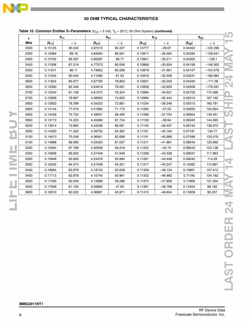
Table 10. Common Emitter S--Parameters (VCC = 5 Vdc, TA = 25C, 50 Ohm System) (continued)
fMHz
S11 S21 S12 S22
|S11| |S21| |S12| |S22|
2300 0.10125 90.343 4.87215 90.327 0.10777 --28.67 0.04452 --122.296
2350 0.10384 89.16 4.84064 88.561 0.10817 --29.394 0.04294 --129.541
2400 0.10702 88.397 4.80597 86.77 0.10841 --30.211 0.04205 --138.1
2450 0.11008 87.519 4.77373 85.006 0.10869 --30.924 0.04158 --146.363
2500 0.11241 86.11 4.73852 83.289 0.10879 --31.661 0.04157 --154.578
2550 0.11540 85.045 4.71080 81.53 0.10916 --32.408 0.04231 --162.984
2600 0.11824 83.877 4.67765 79.803 0.10931 --33.203 0.04340 --171.06
2650 0.12090 82.346 4.64616 78.061 0.10958 --33.929 0.04508 --178.591
2700 0.12340 81.156 4.61372 76.324 0.10994 --34.621 0.04725 174.366
2750 0.12606 79.687 4.58063 74.605 0.10994 --35.444 0.05010 167.162
2800 0.12922 78.399 4.55022 72.881 0.11034 --36.246 0.05315 160.781
2850 0.13144 77.016 4.51863 71.172 0.11063 --37.03 0.05620 154.624
2900 0.13428 75.734 4.49057 69.495 0.11089 --37.754 0.06004 149.451
2950 0.13713 74.325 4.45366 67.734 0.11109 --38.64 0.06342 144.065
3000 0.13914 72.892 4.42536 66.061 0.11140 --39.407 0.06743 138.972
3050 0.14320 71.422 4.39730 64.387 0.11161 --40.164 0.07181 134.77
3100 0.14613 70.248 4.36561 62.698 0.11191 --40.968 0.07596 130.079
3150 0.14898 69.069 4.33420 61.007 0.11211 --41.861 0.08043 125.992
3200 0.15264 67.768 4.30556 59.316 0.11252 --42.74 0.08543 122.138
3250 0.15656 66.632 4.27446 57.648 0.11258 --43.528 0.09047 117.963
3300 0.15948 65.655 4.24479 55.984 0.11281 --44.448 0.09540 114.29
3350 0.16325 64.574 4.21546 54.301 0.11317 --45.247 0.10082 110.967
3400 0.16694 63.679 4.18743 52.638 0.11329 --46.134 0.10661 107.412
3450 0.17113 62.876 4.15740 50.961 0.11352 --46.992 0.11195 104.192
3500 0.17493 62.049 4.12688 49.288 0.11374 --47.856 0.11808 101.204
3550 0.17906 61.193 4.09892 47.63 0.11391 --48.768 0.12404 98.182
3600 0.18310 60.522 4.06981 45.971 0.11410 --49.604 0.13009 95.337
LIFETIMEBUY
LASTORDER24
MAY14
LASTSHIP
24MAY15

MMG3011NT1
9RF Device DataFreescale Semiconductor, Inc.
1.7
5.33
3.48
0.581.27
0.86
3.86
0.64
7.62
2.49
2.541.27
0.305 diameter
Figure 20. Recommended Mounting Configuration
NOTES:1. THERMAL AND RF GROUNDING CONSIDERATIONS SHOULD BE
USED IN PCB LAYOUT DESIGN.2. DEPENDING ON PCB DESIGN RULES, AS MANY VIAS AS
POSSIBLE SHOULD BE PLACED ON THE LANDING PATTERN.3. IF VIAS CANNOT BE PLACED ON THE LANDING PATTERN, THEN
AS MANY VIAS AS POSSIBLE SHOULD BE PLACED AS CLOSE TOTHE LANDING PATTERN AS POSSIBLE FOR OPTIMAL THERMALAND RF PERFORMANCE.
4. RECOMMENDED VIA PATTERN SHOWN HAS 0.381 x 0.762 MMPITCH.
Recommended Solder Stencil
Figure 21. Product Marking
M3011N( )
YYWWLIFETIMEBUY
LASTORDER24
MAY14
LASTSHIP
24MAY15

10RF Device Data
Freescale Semiconductor, Inc.
MMG3011NT1
PACKAGE DIMENSIONS

MMG3011NT1
11RF Device DataFreescale Semiconductor, Inc.

12RF Device Data
Freescale Semiconductor, Inc.
MMG3011NT1

MMG3011NT1
13RF Device DataFreescale Semiconductor, Inc.
PRODUCT DOCUMENTATION, SOFTWARE AND TOOLS
Refer to the following resources to aid your design process.
Application Notes
AN1955: Thermal Measurement Methodology of RF Power Amplifiers AN3100: General Purpose Amplifier and MMIC BiasingSoftware
.s2p FileDevelopment Tools
Printed Circuit Boards
For Software and Tools, do a Part Number search at http://www.freescale.com, and select the “Part Number” link. Go toSoftware & Tools on the part’s Product Summary page to download the respective tool.
REVISION HISTORY
The following table summarizes revisions to this document.
Revision Date Description
3 Mar. 2007 Corrected and updated Part Numbers in Tables 8 and 9, Component Designations and Values, to RoHScompliant part numbers, pp. 6, 7
4 July 2007 Replaced Case Outline 1514--01 with 1514--02, Issue D, pp. 1, 11--13. Case updated to add missingdimension for Pin 1 and Pin 3.
5 Mar. 2008 Removed Footnote 2, Continuous voltage and current applied to device, from Table 2, Maximum Ratings,p. 1
Corrected Fig. 13, Single--Carrier W--CDMA Adjacent Channel Power Ratio versus Output Power y--axis(ACPR) unit of measure to dBc, p. 5
Corrected S--Parameter table frequency column label to read “MHz” versus “GHz” and correctedfrequency values from GHz to MHz, pp. 8, 9
6 Feb. 2012 Corrected temperature at which ThetaJC is measured from 25C to 87C and added “no RF applied” toThermal Characteristics table to indicate that thermal characterization is performed under DC test with noRF signal applied, p. 1
Table 6, ESD Protection Characterization, removed the word “Minimum” after the ESD class rating. ESDratings are characterized during new product development but are not 100% tested during production. ESDratings provided in the data sheet are intended to be used as a guideline when handling ESD sensitivedevices, p. 3
Removed ICC bias callout from applicable graphs and Table 10, Common Emitter S--Parameters headingas bias is not a controlled value, pp. 4--9
Added .s2p File availability to Product Software and Printed Circuit Boards to Development Tools, p. 14
7 Sept. 2014 Added Fig. 21, Product Marking, p. 9
LIFETIMEBUY
LASTORDER24
MAY14
LASTSHIP
24MAY15

14RF Device Data
Freescale Semiconductor, Inc.
MMG3011NT1
Information in this document is provided solely to enable system and softwareimplementers to use Freescale products. There are no express or implied copyrightlicenses granted hereunder to design or fabricate any integrated circuits based on theinformation in this document.
Freescale reserves the right to make changes without further notice to any productsherein. Freescale makes no warranty, representation, or guarantee regarding thesuitability of its products for any particular purpose, nor does Freescale assume anyliability arising out of the application or use of any product or circuit, and specificallydisclaims any and all liability, including without limitation consequential or incidentaldamages. “Typical” parameters that may be provided in Freescale data sheets and/orspecifications can and do vary in different applications, and actual performance mayvary over time. All operating parameters, including “typicals,” must be validated foreach customer application by customer’s technical experts. Freescale does not conveyany license under its patent rights nor the rights of others. Freescale sells productspursuant to standard terms and conditions of sale, which can be found at the followingaddress: freescale.com/SalesTermsandConditions.
Freescale and the Freescale logo are trademarks of Freescale Semiconductor, Inc.,Reg. U.S. Pat. & Tm. Off. All other product or service names are the property of theirrespective owners.E 2005--2008, 2012, 2014 Freescale Semiconductor, Inc.
How to Reach Us:
Home Page:freescale.com
Web Support:freescale.com/support
Document Number: MMG3011NT1Rev. 7, 9/2014