Embed Size (px)
Citation preview

Nanometer-scale imaging and metrology, nano-fabrication with the
Orion Helium Ion Microscope
Certain commercial equipment is identified in this work to adequately describe the experimental procedure. Such identification does not imply recommendation or endorsement by the National Institute of Standards and Technology, nor does it imply that the equipment identified is necessarily the best available for the purpose.
Bin Ming, András E. Vladár and Michael T. Postek
National Institute of Standards and Technology (NIST)

Helium Ion Microscope (HeIM)
• First of this new type of instrument has been installed at NIST within the Manufacturing Engineering Laboratory, Precision Engineering Division
• In place of electrons, helium ions (He+) are generated and used to irradiate the sample
• Theoretically expected to be 0.25 nm or 4 times better than the best of current large sample SEMs
• Potential applications in patterning at the nanometer scale.

• Resolution– Base System ≤ 0.75 nm– Enhanced Resolution ≤0.35 nm (optional)
• Accelerating Voltage– 30±5 kV fixed
• Beam Current–1fA - 25pA–Typically 0.5-1 pA for Highest Resolution
• Detectors–Everhart Thornley for Secondary Electrons
–MCP for Rutherford Backscattered Ions
• Charge Control–Electron Flood Gun
The HeIM 2009 – ORION│Plus ..... Spec’s

Helium Ion Microscopy for IC Industry• 0.21 nm resolution/focusing ability has been claimed
by vendor
25 % - 75 % signal transition-based resolution (spot size) measurement on an asbestos fiber on a thin holey carbon foil sample. The quoted resolution is 0.21 nm on an image taken on Orion Plus HeIM. The field-of-view is 200 nm (courtesy of Carl Zeiss SMT).
• At this point close to 1 nm resolution is typical

• 1 keV electron beam has a larger interaction volume resulting in SE1 and SE2• 30 kV He beam is still collimated well below the SE escape depth and there is
minimal signal contribution from recoil• HeIM images have a better resolution than a high keV SEM and a smaller
sample interaction volume than a low keV SEM
HeIM – Beam Sample Interaction
Simulation results from TNO-TU Delft

• He+ beam produces both secondary electrons (SE) and backscattered ions
• SE yield is large, so low beam currents work well
• Interaction volume of He+ beam near the surface is thought to be considerably smaller than that of an SEM
• The excited volume is restricted and SE generation is near the surface
• At the same energy, the wavelength of the He ions is much smaller than that of the electrons
Helium Ion Microscope (HeIM)

HeIM Image: High Surface Sensitivity
field of view = 4.5 micrometers field of view = 10.0 micrometers

Comparison of carbon nanotube imaging
SEM image HeIM image field of view = 630 nm field of view = 800nm

SEM image HeIM image field of view = 260 nm field of view = 500nm
Comparison of magnetic tape resolution sample images

HeIM and SEM Depth of Field
High vacuum, medium landing energy SEM image of Au-decorated tin ball resolution
sample. 1.5 mm field of view
High vacuum, high landing energy helium ion microscope (HeIM) image of Au-decorated tin ball resolution sample. 1.5 mm field of
view

HeIM Depth of Field for large samples

HeIM imaging of Resist Samples
40 nm wide resist patterns showing wall roughness, 0.1 pA beam current, 1 mm field of
view.
Tilted view of resist wide lines on Si, 1.4 mm field of view.
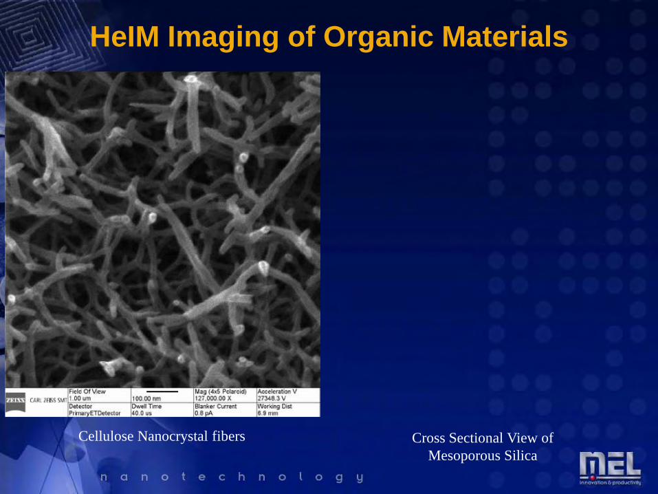
HeIM Imaging of Organic Materials
Cellulose Nanocrystal fibers Cross Sectional View of Mesoporous Silica

Metrology Example: Poly Line-Space Array
• Sub-100nm lines• Single line scans at positions indicated• HeIM line scan shows extremely sharp
drop to substrate signal level.
100nm
100nm
0
50
100
150
200
250
-5 15 35 55 75
Distance, nm
Imag
e gr
ay le
vel
SEM
Orion

HeIM imaging of Amorphous Si
Amorphous Si on Si sample showing swelling due to He ion irradiation. 2 pA beam current, 2 mm
field of view.
65 nm wide amorphous Si lines on Si, 1 mm field of view.
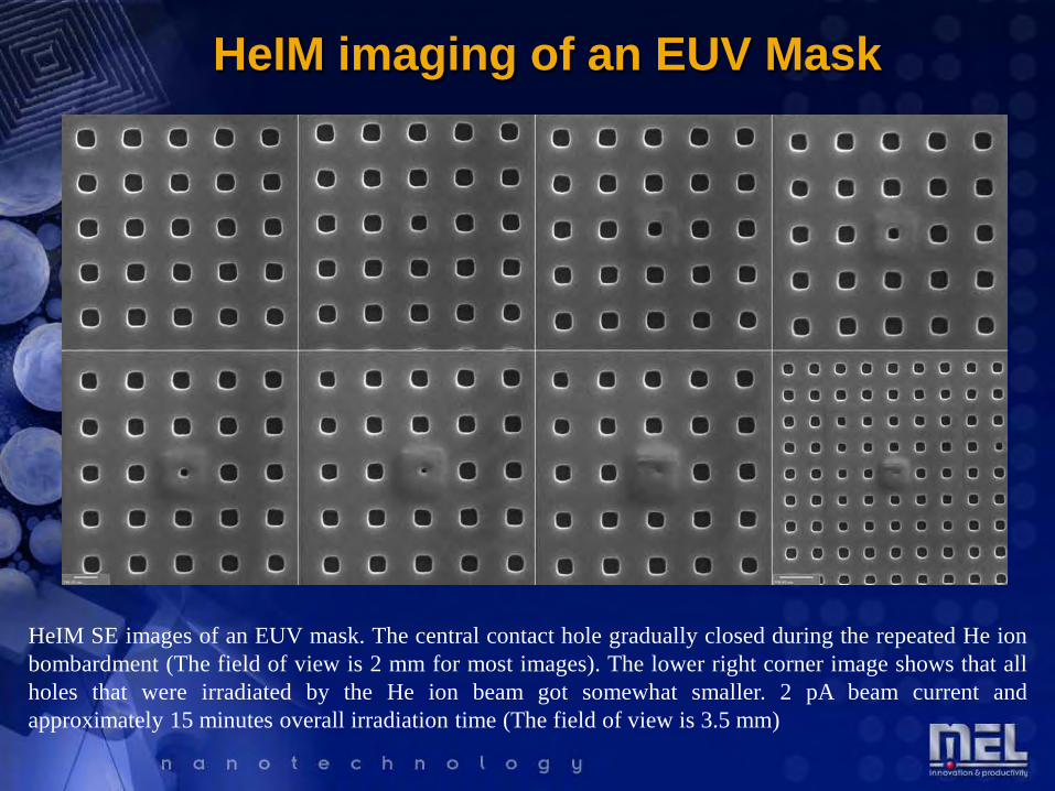
HeIM imaging of an EUV Mask
HeIM SE images of an EUV mask. The central contact hole gradually closed during the repeated He ionbombardment (The field of view is 2 mm for most images). The lower right corner image shows that allholes that were irradiated by the He ion beam got somewhat smaller. 2 pA beam current andapproximately 15 minutes overall irradiation time (The field of view is 3.5 mm)

HeIM Nano-Milling
• HeIM SE image of30 nm Au particlesample after nano-milling. 700 nmfield of view
• An aperture of 10 nmsize created by HeIMnano-milling. 800 nmfield of view
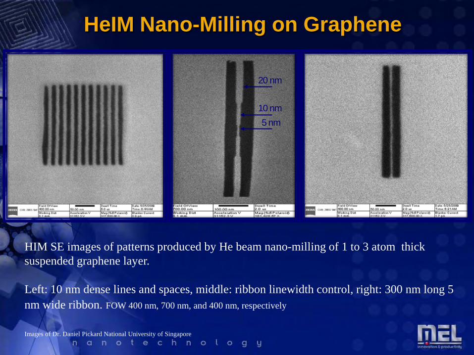
HeIM Nano-Milling on Graphene
HIM SE images of patterns produced by He beam nano-milling of 1 to 3 atom thick suspended graphene layer.
Left: 10 nm dense lines and spaces, middle: ribbon linewidth control, right: 300 nm long 5 nm wide ribbon. FOW 400 nm, 700 nm, and 400 nm, respectively
Images of Dr. Daniel Pickard National University of Singapore
5 nm
10 nm
20 nm
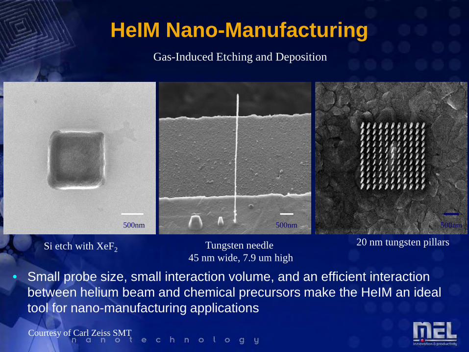
• Small probe size, small interaction volume, and an efficient interaction between helium beam and chemical precursors make the HeIM an ideal tool for nano-manufacturing applications
HeIM Nano-Manufacturing
500nm 500nm500nm
Si etch with XeF2 Tungsten needle 45 nm wide, 7.9 um high
20 nm tungsten pillars
Gas-Induced Etching and Deposition
Courtesy of Carl Zeiss SMT

High-Throughput Helim Ion Lithography
Dense array of 15 nm hydrogen silsesquioxane (HSQ) resist posts generated by He ion lithography 500 nm field of view (left) and 180 nm field of view (right).
• Very low dose is enough to expose resist• 1000 fold speed advantage over e-beam litho
might be possible

High Aspect Ratio Patterning by Helium Ion Lithography

Scanning Electron Microscope Helium Ion Microscope
Penetration effects limit surface detail Excellent surface detail
Positive and negative electron charging possible
Positive charging possible but can be eliminated by electron flood gun
High beam currents might result in sample damage
High beam currents/doses result in sample damage (milling, swelling)
X-ray analysis possible Other analytical modes need to be pursued
Surface contamination possible but masked by high kV operation
Surface contamination can be a bigger problem
Electromagnetic fields are likely to limit operation
Electromagnetic fields are less likely to limit operation
Mechanical vibration limits high-resolution operation
Mechanical vibration is a serious limit to high-resolution operation
Established and relative mature emitter technology
Emitter technology is still in development
Source demagnification at sample 100-12,000 x depending on column design
Source demagnification ~3-50 x
Lithography, material deposition possible Nano-milling, lithography and material deposition possible

Helium Ion Microscopy• The helium ion microscope (HeIM) is reaching a stage of
maturity. It’s highly desirable to explore what this technology could bring to the various industries.
• Foreseeable applications include– Dimensional metrology of resist and developed wafers– Dimensional metrology of traditional and advanced masks– Ion beam lithography (very high sensitivity/throughput) – Mask fabrication and repair– Nano-etching, nano-scale deposition– Direct device fabrication/alteration– Particle composition analysis at the nm scale
• Useful simulation modeling software package is available already.

HeIM and FIB
• FIB and HeIM– Each has unique
advantages/strengths– Remain complimentary
• As a revolutionary technology, HeIM is forging new ground for both imaging and patterning at the nanoscale.


![mailto:richard.davis@fmglobal.com] - nist.gov](https://img.dokumen.tips/doc/110x75/6299b29681e8d526d1386d99/mailto-fmglobalcom-nistgov.jpg)