Embed Size (px)
Citation preview

Harsh Environment Silicon Carbide UV Sensor and Junction Field-Effect Transistor
By
Wei-Cheng Lien
A dissertation submitted in partial satisfaction of the
requirements for the degree of
Doctor of Philosophy
in
Applied Science & Technology
in the
Graduate Division
of the
University of California, Berkeley
Committee in charge:
Professor Albert P. Pisano, Chair
Professor Tsu-Jae King Liu
Professor Elad Alon
Fall 2013

Harsh Environment Silicon Carbide UV Sensor and Junction Field-Effect Transistor
Copyright © 2013
by
Wei-Cheng Lien

1
Abstract
Harsh Environment Silicon Carbide UV Sensor and Junction Field-Effect Transistor
by
Wei-Cheng Lien
Doctor of Philosophy in Applied Science & Technology
University of California, Berkeley
Professor Albert P. Pisano, Chair
A harsh environment can be defined by one or more of the following: High temperature,
high shock, high radiation, erosive flow, and corrosive media. Among all the harsh
environment applications, high temperature applications have drawn lots of attention due
to the emerging activity in automotive, turbine engine, space exploration and deep-well
drilling telemetry. Silicon carbide has become the candidate for these harsh environment
applications because of its wide bandgap, excellent chemical and thermal stability, and
high breakdown electric field strength. This dissertation details the two building blocks of
high-temperature UV sensing chip, namely Ultraviolet sensor and transistors. High
temperature performance of silicon carbide metal-semiconductor-metal UV sensor is
characterized at high temperatures for the first time. The sensor exhibits high photo-to-
dark current ratio and fast rise and fall time even at high temperatures. Complementary
SiC junction field-effect transistors of different gate configurations are proposed,
fabricated and characterized from room temperature to 600 °C for the first time. High
intrinsic gains at high temperatures suggest that complementary junction field-effect
transistors are suitable devices for high temperature operational amplifier.

i
Contents
Contents i
List of Figures iv
List of Tables x
Acknowledgements xii
1. Introduction 1
1.1 Harsh Environment Sensing Application……………………………………...1
1.2 Silicon Carbide………………………………………………………………...2
1.3 SiC Sensors for High Temperature Application………………………………5
1.3.1 UV Sensor…………………………………………………………...5
1.3.2 Pressure Sensor……………………………………………………...5
1.4 SiC Electronics Low Voltage High Temperature Application………………..6
1.5 High Temperature Effects in 4H-SiC…………………………………………8
1.6 Research Objective and Thesis Overview…………………………………….9
1.7 References ……………………………………………………………………10
2. Silicon Carbide Metal-Semiconductor-Metal Ultraviolet Photodetectors 14
2.1 Introduction…………………………………………………………………..14
2.2 Physics of MSM Photodetectors……………………………………………..15
2.3 4H-SiC MSM Photodetectors………………………………………………..17
2.3.1 Fabrication Process and Characterization Methods………………..17
2.3.2 Characterization of 4H-SiC Thin Films ……………………………18
ii
2.3.3 Characterization of 4H-SiC MSM Photodetector………………….19
2.4 Antireflection Layer Using Nanostructure…………………………………...23
2.5 Summary……………………………………………………………………..25
2.6 References ……………………………………………………………………26
3. Silicon Carbide N-Channel Raised Gate Junction Field-Effect Transistors 28
3.1 Introduction…………………………………………………………………..28
3.2 Physics of JFET……………………………………………………………...28
3.3 Fabrication Process…………………………………………………………..32
3.4 Metallization of N-Channel Raised Gate JFET……………………………...37
3.5 Electrical Properties of N-Channel Raised Gate JFET………………………43
3.5.1 Characterization of N-JFET at Room Temperature………………..43
3.5.2 Characterization of N-JFET at High Temperatures………………..45
3.5.3 Reliability…………………………………………………………..48
3.6 TCAD Simulation of N-Channel Raised Gate JFET………………………...50
3.7 SPICE Parameter Extraction and Device Modeling…………………………53
3.8 Summary……………………………………………………………………..55
3.9 Reference…………………………………………………………………….55
4. Silicon Carbide Complementary Buried Gate Junction Field-Effect Transistors 59
4.1 Introduction…………………………………………………………………..59
4.2 Design of Complementary Buried Gate JFET……………………………….59
4.3 Fabrication Process…………………………………………………………..64
4.4 Metallization of Complementary Buried Gate JFET………………………...68
4.5 Electrical Properties of N-Channel Buried Gate JFET………………………71
4.6 Electrical Properties of P-Channel Buried Gate JFET……………………….73

iii
4.6.1 Characterization of P-Channel Buried Gate JFET at Room
Temperature……………………………………………………………………...73
4.6.2 Characterization of P-Channel Raised Gate JFET at High
Temperature……………………………………………………………………...75
4.7 Summary……………………………………………………………………..79
4.8 Reference…………………………………………………………………….79
5. Conclusion and Future Work 82
5.1 Contributions of This Work………………………………………………….82
5.2 Integrated SiC Sensor Design Challenges…………………………………...83
5.3 Reference…………………………………………………………………….83
iv
List of Figures
Figure 1.1: The structure of SiC crystal…………………………………………………...2
Figure 1.2: Three most common polytypes of silicon carbide. Copyright: Dr. Christopher
S. Roper …………………………………………………………………………………...3
Figure 1.3: Bi-layer stacking for the SiC polytypes 3C, 2H, 4H, and 6H.………………..3
Figure 1.4: Calculated energy bandgap of Si, 6H-SiC, and 4H-SiC versus temperature…8
Figure 1.5: Intrinsic carrier concentration in Si, 6H-SiC, and 4H-SiC versus
temperature………………………………………………………………………………..9
Figure 2.1: Schematic of MSM photodetector…………………………………………...15
Figure 2.2: (a) The MSM photodetector is considered as two back-to-back Schottky
barriers. Energy-band diagrams of MSM PDs at equilibrium (b) with n-type
semiconductor layers and (c) with p-type semiconductor layers………………………...16
Figure 2.3: Energy-band diagrams of MSM PDs for p-type semiconductor (a) without
light and (b) with light at flat-band voltage……………………………………………...16
Figure 2.4: (a) Schematic and (b) optical image of 4H-SiC MSM PDs…………………17
Figure 2.5: Schematic of time-resolved measurement system…………………………...18
Figure 2.6: (a) Cross-sectional TEM image and (b) electron diffraction pattern of
epitaxial p-type 4H-SiC layer……………………………………………………………19
Figure 2.7: The transmission spectrum (left y axis) and (αhυ)2
(right y axis) vs. hυ plot of
4H-SiC substrates………………………………………………………………………...19
Figure 2.8: I-V curves of the 4H-SiC MSM PDs measured in the dark and under 325-nm
illumination at room temperature………………………………………………………...20
Figure 2.9: The time dependence of the photocurrent and dark current of SiC MSM PDs
at 25 °C under a 5 V bias………………………………………………………………...21
v
Figure 2.10: (a) PDCR value and (b) responsivity as function of temperature under a 5 V
bias……………………………………………………………………………………….21
Figure 2.11: The time dependence of the photocurrent and dark current of SiC MSM PDs
at 450 °C under a 5 V bias……………………………………………………………….22
Figure 2.12: The transient photocurrent of SiC MSM PDs at room temperature and 400
°C under a 5 V bias………………………………………………………………………22
Figure 2.13: (a) Top view and (b) cross-sectional SEM image of ZnO NRA/SiC
layers……………………………………………………………………………………..24
Figure 2.14: Reflectance spectra of (a) bare SiC MSM PDs and (b) ZnO NRA/ SiC MSM
PDs with a wide range of AOIs………………………………………………………….25
Figure 2.15: FDTD simulation of time-averaged and normalized TE electric field
distribution at 532 nm (a) without and (b) with ZnO NRAs. The insets in (a) and (b) are
the enlarged images at the top SiC surface………………………………………………25
Figure 3.1: Visualization of various phases of JFET operation and the corresponding ID-
VD characteristics at VGS = 0 V. Note the SiC substrate serves as the body biasing point.
The blue color in schematic represents the depletion regions, and the yellow color shows
the channel region. The shape of the channel is for the purpose of demonstration and it is
not the real situation……………………………………………………………………...31
Figure 3.2: Schematic of a lateral n-channel raised gate 4H-SiC JFET…………………32
Figure 3.3: Completed fabrication process flow of 4H-SiC JFET and MSM
photodetectors……………………………………………………………………………33
Figure 3.4: Simulated doping profile of heavily doped drain and source region……......34
Figure 3.5: (a) Cross-sectional scanning TEM image (b) Electron diffraction of implanted
area after annealing at 1450 °C under Argon atmosphere for 30 minutes……………….35
Figure 3.6: AFM images of SiC samples before annealing and after annealing at 1450 °C
under Argon atmosphere for 30 minutes………………………………………………...35
Figure 3.7: Fabricated 3” 4H-SiC wafer…………………………………………………36
Figure 3.8: High temperature probe station……………………………………………...36
Figure 3.9: HP 4156B semiconductor parameter analyzer and Agilent B2912A precision
source/measurement unit………………………………………………………………...37
vi
Figure 3.10: Ideal Ohmic contact of metal with (a) p-type semiconductor and (b) n-type
semiconductor……………………………………………………………………………38
Figure 3.11: Several metal workfunctions compared with the 4H-SiC band diagram…..38
Figure 3.12: Optical image of TLM structure……………………………………………39
Figure 3.13: Measure I-V curves of metal and n-type 4H-SiC before and after RTA
annealing for TLM structure with d = 80 µm……………………………………………40
Figure 3.14: Measured resistance between contacts vs. different distances at room
temperature of Ti/Ni/TiW metal stacks and n-type 4H-SiC……………………………..41
Figure 3.15: Temperature dependences of specific contact resistance of Ti/Ni/TiW metal
stacks to n+ 4H-SiC………………………………………………………………………42
Figure 3.16: Measure I-V curves of metal and p-type 4H-SiC for TLM structure with d =
5 µm……………………………………………………………………………………...43
Figure 3.17: Optical image of a n-channel raised gate 4H-SiC JFET with L = 10 μm and
W = 100 μm………………………………………………………………………………44
Figure 3.18: IDS-VDS characteristics of a n-channel 4H-SiC JFET (a) before RTA (b) after
RTA under different VGS and with W/L= 100 μm/10 μm at 25 °C………………………44
Figure 3.19: (a) IDS-VGS (b) √ -VGS characteristics of a n-channel 4H-SiC JFET with
W/L= 100 μm/10 μm and VDS = 20 V at 25 °C…………………………………………..44
Figure 3.20: IDS-VDS characteristics of a n-channel 4H-SiC JFET under different VGS and
with W/L= 100 μm/10 μm (a) at 110 °C (b) at 210 °C (c) at 300 °C (d) at 400 °C (e) at
500 °C (f) at 550 °C (g) at 600 °C. (h) Temperature dependences of IDsat of a n-channel
4H-SiC JFET at VGS = 0 V and with W/L= 100 μm/10 μm……………………………...46
Figure 3.21: (a) IDS-VGS (b) √ -VGS characteristics of a n-channel 4H-SiC JFET under
VDS = 20 V and with W/L= 100 μm/10 μm at different temperatures……………………47
Figure 3.22: Temperature dependence of threshold voltage of a n-channel 4H-SiC JFET
with W/L= 100 μm/10 μm…………………………………………………………….….47
Figure 3.23: Temperature dependence of transconductance and intrinsic gain of of a n-
channel 4H-SiC JFET with W/L= 100 μm/10 μm………………………………………..48
Figure 3.24: (a) IDS-VDS characteristics at VGS = 0 V and (b) IDS-VGS characteristics at VDS
= 20 V during 0, 25th, 50th, 75th, and 90 hours of electrical operation at 540 °C for a n-
channel 4H-SiC JFET with W/L = 100 μm/10 μm ………………………………………49

vii
Figure 3.25: Normalized gm versus test time at 540 °C through 90 hours for a n-channel
4H-SiC JFET with W/L = 100 μm/10 μm………………………………………………..50
Figure 3.26: Optical image of a n-channel 4H-SiC JFET with W/L = 100 μm/10 μm after
thermal reliability test at 540 °C after 90 hours………………………………………….50
Figure 3.27: Raised gate JFET structure generated by the Sentaurus structure editor…..52
Figure 3.28: Measured and Simulated (a) IDS-VDS characteristics at VGS = 0 V and (b) IDS-
VGS characteristics at VDS = 20 for n-channel 4H-SiC JFETs with W/L = 100 μm/10 μm at
25 and 600 °C……………………………………………………………………………52
Figure 3.29: Arrhenius plot of log of drain leakage current versus 1/T at VGS = -10 V of a
n-channel 4H-SiC JFET with W/L = 100 μm/10 μm…………………………………….52
Figure 3.30: Modeled and measured IDS-VDS characteristics of a n-channel 4H-SiC JFETs
under different VGS and with W/L= 100 μm/10 μm (a) at 110 °C (b) at 210 °C (c) at 300
°C (d) at 400 °C (e) at 500 °C (f) at 600 °C. The black dot lines are modeled devices and
the red solid lines are measured devices. From the top curve to the bottom curve, VGS are
0, -2, -4, -6, -8 V, respectively…………………………………………………………...54
Figure 4.1: Buried gate JFET structure generated by the Sentaurus structure editor……60
Figure 4.2: Simulated IDS-VGS of n-channel JFETs with L = 8 µm and (a) different
channel doping with fixed channel depth of 250 nm (b) different channel depth with fixed
channel doping of 2.5×10¹⁷
cm-3
at 25 °C..……………………………………………...60
Figure 4.3: Simulated IDS-VGS of p-channel JFETs with L = 8 µm and (a) different
channel doping with fixed channel depth of 400 nm (b) different channel depth with fixed
channel doping of 1.5×10¹⁷
cm-3
at 25 °C..……………………………………………...61
Figure 4.4: Simulated IDS-VGS of a (a) n-channel (b) p-channel JFET with L = 8 µm…...61
Figure 4.5: Temperature dependence of (a) carrier mobility and (b) degree of
ionization............................................................................................................................64
Figure 4.6: Schematic of 4H-SiC complementary JFETs………………………………..65
Figure 4.7: Completed fabrication process flow of 4H-SiC c-JFETs……………………66
Figure 4.8: Simulated phosphorous doping profile in the p-channel area with NA =
1.5×10¹⁷
cm-3
…………………………………………………………………………….67
Figure 4.9: Simulated aluminum doping profile in the n-channel area with ND = 2.5×10¹⁷
cm-3
………………………………………………………………………………………67

viii
Figure 4.10: SEM image of etching pits after thermal annealing at 1550 °C for 15
minute……………………………………………………………………………………68
Figure 4.11: Measure I-V curves of metal and n-type 4H-SiC before and after RTA
annealing for TLM structure with d = 5 µm……………………………………………..69
Figure 4.12: Temperature dependences of specific contact resistance of Ni/Ti/Al/TiW
metal stacks to n+ 4H-SiC………………………………………………………………..69
Figure 4.13: Measure I-V curves of metal and p-type 4H-SiC before and after RTA
annealing for TLM structure with d = 20 µm……………………………………………70
Figure 4.14: Temperature dependences of specific contact resistance of Ni/Ti/Al/TiW
metal stacks to p+ 4H-SiC………………………………………………………………..71
Figure 4.15: Optical image of a n-channel buried gate 4H-SiC JFET with L = 10 μm and
W = 100 μm………………………………………………………………………………72
Figure 4.16: IDS-VDS characteristics of a n-channel buried gate 4H-SiC JFET under
different VGS and with W/L= 100 μm/10 μm at 25 °C…………………………………...72
Figure 4.17: I-V characteristics of pn junction in the n-channel buried gate 4H-SiC JFET
structure.………………………………………………………………………………….73
Figure 4.18: Optical image of a p-channel buried gate 4H-SiC JFET with L = 10 μm and
W = 100 μm………………………………………………………………………………74
Figure 4.19: |IDS|-VDS characteristics of a p-channel 4H-SiC JFET under different VGS and
with W/L= 100 μm/10 μm at 25 °C………………………………………………………74
Figure 4.20: (a) |IDS|-VGS (b) √ -VGS characteristics of a p-channel 4H-SiC JFET with
W/L= 100 μm/10 μm and VDS = -20 V at 25 °C………………………………………….75
Figure 4.21: IDS-VDS characteristics of a p-channel 4H-SiC JFET under different VGS and
with W/L= 100 μm/10 μm (a) at 110 °C (b) at 210 °C (c) at 300 °C (d) at 400 °C (e) at
500 °C (f) at 550 °C (g) at 600 °C. (h) Temperature dependences of IDsat of a p-channel
4H-SiC JFET at VGS = 0 V and with W/L= 100 μm/10 μm……………………………...76
Figure 4.22: |IDS|-VGS characteristics of a p-channel 4H-SiC JFET under VDS = -20 V and
with W/L= 100 μm/10 μm at different temperatures…………………………………….77
Figure 4.23: Temperature dependence of threshold voltage of a p-channel 4H-SiC JFET
with W/L= 100 μm/10 μm………………………………………………………………..78

ix
Figure 4.24: Temperature dependence of transconductance and intrinsic gain of of a p-
channel 4H-SiC JFET with W/L= 100 μm/10 μm………………………………………..78
x
List of Tables
Table 1.1: High temperature electronics applications……………………………………..2
Table 1.2: Mechanical properties of Si and wide bandgap semiconductors. If the thermal
expansion coefficient has two values, the first one is along the a-axis and the second one
is along the c-axis…………………………………………………………………………4
Table 1.3: Electrical properties of Si and wide bandgap semiconductors. If the electron
mobility has two values, the first one is perpendicular to the c-axis and the second one is
parallel to the c-axis……………………………………………………………………….4
Table 1.4: A sampling of published single transistors for high temperature applications...7
Table 2.1: Response time of fabricated 4H-SiC MSM photodetectors………………….23
Table 3.1: Specific contact resistance measurements on 4H-SiC in the literature………41
Table 3.2: Sheet resistance and specific contact resistance of Ti/Ni/TiW metal stacks and
n-type 4H-SiC at different temperatures…………………………………………………42
Table 3.3: Extracted parameters of n-channel raised gate 4H-SiC JFET with W/L= 100
μm/10 μm at various temperatures. gm, Ron, ro , λ and gmro is based on VGS = 0 V. IDsat/Ioff
is the ratio of current at VGS = 0 V and VGS = -9 V………………………………………48
Table 3.4: The extracted SPICE parameters of a n-channel 4H-SiC JFET with W/L= 100
μm/10 μm from 25 to 600 °C…………………………………………………………….53
Table 4.1: Optimized parameters of complementary JFETs with L = 10 µm. gm, ro, and
gmro is based on VGS = 0 V……………………………………………………………….62
Table 4.2: Fitting parameters for low field mobility of 4H-SiC…………………………63
Table 4.3: Sheet resistance and specific contact resistance of Ni/Ti/Al/TiW metal stacks
and n-type 4H-SiC at different temperatures…………………………………………….70
Table 4.4: Sheet resistance and specific contact resistance of Ni/Ti/Al/TiW metal stacks
and p-type 4H-SiC at different temperatures…………………………………………….71

xi
Table 4.5: Extracted parameters of a p-channel buried gate 4H-SiC JFET with W/L= 100
μm/10 μm at various temperatures. gm, Ron, ro , λ and gmro is based on VGS = 0 V. IDsat/Ioff
is the ratio of current at VGS = 0 V to current at VGS = 7 V………………………………79

xii
Acknowledgments
There are many people who deserve my acknowledgments during the three and
half years of my Ph. D. study at the University of California at Berkeley. I would like to
express my sincere thanks to my advisor, Professor Albert P. Pisano. He is a caring
advisor offering me endless help on my research, course work and even life at Berkeley.
He gives me the freedom to explore interesting research topics and encourages me, rather
than blaming me, when I am frustrated and make mistakes.
I am also grateful for the support from my dissertation committee members
Professor Tsu-Jae King Liu and Professor Elad Alon.
Professors Debbie Senesky, Roya Maboudian, Ali Javey, and Roger Howe have
provided me with many inspiring ideas and invaluable advice. The members of the
Pisano lab, past and present, have taught me the skills, techniques and valuable
discussions for this work. In addition, Dr. Louis Hutin and Nattapol Damrongplasit from
Professor Tsu-Jae King Liu's group, and Jun-Chau Chien from Professor Ali Niknejad’s
group, and Yang Lin and Wei-Chun Li from Professor Clark Nguyen's group shared their
knowledge and offered valuable help for me. I would like to thank the staff at Berkeley
Marvell Nanolab for providing much assistance related to operating the machines in
Nanolab. I also want to thank the staff of the BSAC and ERSO office for helping with
purchase orders and grant administration.
My wonderful friends, Fabian Goericke, Matt Chan, Yegan Erdem, Albert Gutes,
Ting-Ta Yen, Chih-Ming Lin, Yun-Ju Lai, Ting-Ying Chung, Chih-Wei Chu, Stefano
Fissolo, Kuo-Ken Huang and Terry Tsai, deserve my special thanks for their unremitting
support and encouragement with everything.
Finally, and most importantly, I want to express my deepest gratitude to my
parents and two sisters for their love.

1
Chapter 1
Introduction
1.1 Harsh Environment Sensing Application
Recently, much research effort has focused on advancing renewable energy
resources, such as solar, hydro, wind and geothermal energy. While developing these new
technologies, reducing inefficiencies in generation and transmission should be considered.
For example, the total energy lost is 61% of energy supply in U.S. in 2012 [1]. One
method of addressing the inefficiencies in energy use is through the development of harsh
environment sensing technology. Power systems can be advanced by integration of
electronics (e.g., communication, signal processing, microactuator control, etc.) to
operate at high temperature [2, 3]. Specifically, smart harsh environment electronic
sensing systems enable real-time condition based monitoring of temperature and
incomplete combustion, and reduce emission of greenhouse gases (NOx and CO2) in gas
turbine system or combustion engine [4, 5]. In addition, wireless technology helps
telemetry systems to guide deep-well oil drilling operation or monitors the subsurface
environments found in geothermal power plants.
A harsh environment can be defined by one or more of the following: High
temperature (> 350 °C), high shock (> 50,000 g), high radiation (> 100 Mrads), erosive
flow, and corrosive media [6]. Silicon is a widely used semiconductor material because
of such factors as its high quality, stable oxide, and low cost. However silicon-based
microelectronics are not suitable for harsh environments, because the electronic
properties of silicon degrade above 300 °C due to the more intrinsic carrier presented
than dopant carriers and mechanical properties degrade above 600 °C due to decline in its
elastic modulus [3]. As the need increases for electronics and microelectromechanical
systems (MEMS) devices suitable for harsh environment applications, including
automobile, aerospace, nuclear and military purposes, several technologies such as
silicon-on-insulator (SOI) or wide bandgap (WBG) electronics are needed. SOI
technology can extend the CMOS operating temperature due to reduce leakage and less
parasitic bipolar action [7]. A wide bandgap material has large energy bandgap of 3 eV so
the generation of intrinsic carriers will not surpass the dopant carriers at high temperature.
In order to realize integration of the sensing system, the building blocks of the
sensor system, such as sensors and transistors, need to be developed. Among all the harsh
environment applications, high temperature applications have drawn lots of attention due
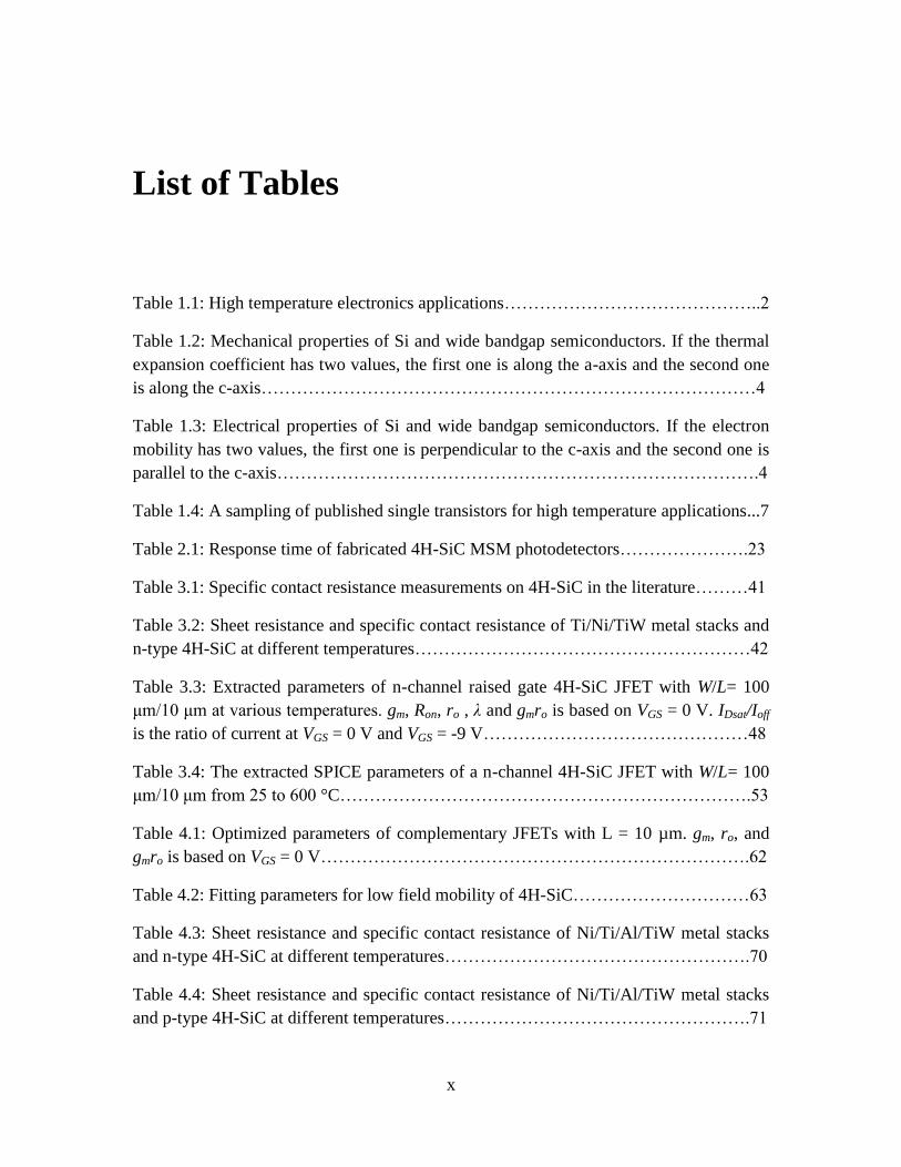
to the emerging activity in several areas (Table 1.1) [3]. In this work, we focus on
2
developing the sensor and electronics for high temperature application. Silicon carbide
(SiC) has been chosen as the base semiconductor material for this work due to its wide
bandgap, high electric field breakdown strength, high thermal conductivity, and high
saturated carrier drift velocity [8].
Application Area
Peak
ambient
(°C)
Chip
power
(kW)
Target technology
Autimotive
On-cylinder
& Exhaust
pipe
600 < 1 WBG
Turbine engine
Sensors,
telemetry,
control
600 < 1 WBG
Electric
actuation 600 > 10 WBG
Spacecraft Power
management 300 > 10 WBG
Venus &
Mercury
exploration
550 1 WBG
Industrial
High
temperature
processing
600 < 1 SOI & WBG
Deep-well drilling telemetry Oil and gas 300 < 1 SOI & WBG
geothermal 600 < 1 WBG
Table 1.1: High temperature electronics applications.
1.2 Silicon Carbide
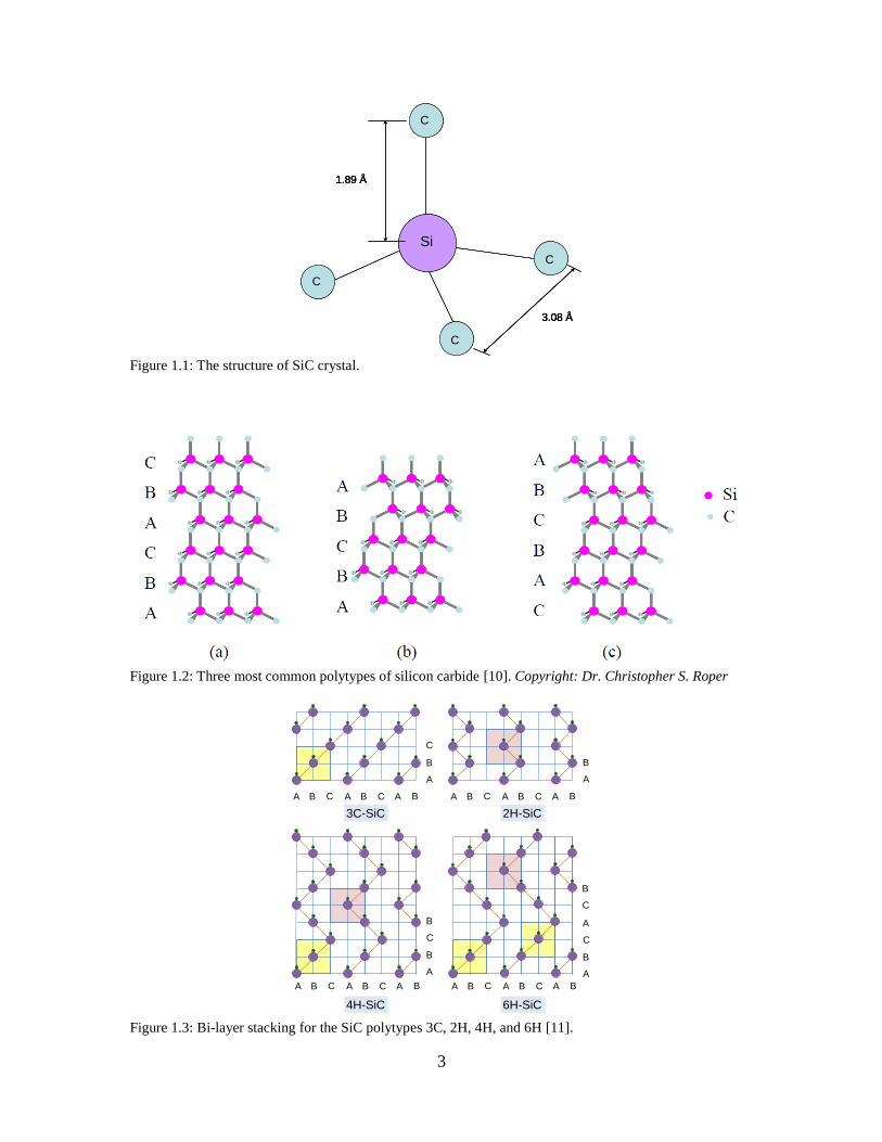
The silicon carbide unit cell is a tetrahedron consisting of four carbon atoms with
a silicon atom in the center, as shown in Figure 1.1. There are approximately 200
polytypes of SiC existing in the world [9]. Figure 1.2 shows the three most common
polytypes of silicon carbide, consisting of different stacking sequences of SiC bilayer.
They are cubic (3C, β-SiC) and hexagonal (H, α-SiC) with the number denoting the
number of SiC bilayer stackings [10]. Because of the possible stacking sequences of SiC
bilayer, there are lattice sites in SiC that have a surrounding layer stacking in hexagonal
form and others with cubic form, which are denoted hexagonal sites and cubic sites,
respectively [11]. Figure 1.3 shows that 3C-SiC has one cubic site and 2H-SiC includes
only one hexagonal site. 4H-SiC has one hexagonal and one cubic site, while 6H-SiC
exhibits one hexagonal and two cubic sites. 4H-SiC and 6H-SiC polytypes already have
commercially available wafers and epitaxy, while 3C-SiC is the only polytype that can be
grown heteroepitaxially on a Si wafer. The basic mechanical and electrical properties of
the three SiC polytypes, as well as those for Si, GaN, AlN, and diamond are shown in
Table 1.2 and 1.3 [11-13].
3
Figure 1.1: The structure of SiC crystal.
Figure 1.2: Three most common polytypes of silicon carbide [10]. Copyright: Dr. Christopher S. Roper
Figure 1.3: Bi-layer stacking for the SiC polytypes 3C, 2H, 4H, and 6H [11].
Si
C
C
C
C
1.89 Å
3.08 Å
Si
C
C
C
C
Si
C
C
C
C
1.89 Å
3.08 Å
1.89 Å
3.08 Å
A B C A B C A B
A
B
C
3C-SiC
A B C A B C A B
A
B
2H-SiC
A B C A B C A B
A
B
4H-SiC
C
B
A B C A B C A B
A
B
6H-SiC
C
A
C
B

4
Si 3C-SiC 6H-SiC 4H-SiC 2H-GaN 2H-AlN Diamond
Lattice a
(Ả) 5.43 4.36 3.08 3.08 3.189 3.112 3.567
Lattice c
(Ả) NA NA 15.12 10.08 5.185 4.982 NA
Thermal
expansion
coefficient
(10-6
/K)
2.6 3.28 3.35/3.25 3.3/3.16 5.59/3.17 5.27/4.15 0.8
Density
(g/cm3)
2.33 3.21 3.21 3.21 6.15 3.23 3.5
Thermal
conductivi
ty (W/cm
K)
1.5 3.6 4.9 4.9 1.3 2.85 20
Melting
point (°C) 1420 2830 2830 2830 2500 3000 4000
Mohs
hardness 7 9 9 9 7 10
Table 1.2: Mechanical properties of Si and wide bandgap semiconductors. If the thermal expansion
coefficient has two values, the first one is along the a-axis and the second one is along the c-axis.
Si 3C-SiC 6H-SiC 4H-SiC 2H-GaN 2H-AlN Diamond
Energy
bandgap
(eV)
1.12 2.4 3.0 3.23 3.4 6.2 5.6
Breakdown
field(MV/c
m)
0.25 2.5 2.5 2.2 3.0 2.0 20
Electron
saturation
velocity (107
cm/s)
1.0 2.5 2.0 2.0 2.5 2.0 2.7
Electron
mobility
(Cm/V s)
1400 1000 500/100 950/1150 1245 135 2200
Hole
mobility
(cm/V s)
600 50 80 120 370 14 1600
Dielectric
constant 11.9 9.7 10.0 10.0 9.5 8.5 5.5
Table 1.3: Electrical properties of Si and wide bandgap semiconductors. If the electron mobility has two
values, the first one is perpendicular to the c-axis and the second one is parallel to the c-axis.
Owing to its superior mechanical properties, SiC is quite suitable for
Microelectromechanical systems (MEMS). SiC based MEMS devices have been
previously used as temperature and pressure sensors in a high temperature environment
[14], high-g accelerometers [15], biomedical sensors [16], and strain sensor [5]. SiC may
also be suitable for high frequency MEMS resonators as micromechanical oscillators and

5
filters due to its high E/ρ ratio. The resonant frequency of a micromachined device can be
expressed as
√
(1.1)
where C is constant, f is a function of Poisson’s ratio, E is the material Young’s modulus
and ρ is the material density. SiC has been successfully used to fabricate Lamé mode
MEMS resonators for signal processing [17].
SiC may be used for high temperature, high power, high frequency and radiation
resistance electronics applications. For example, its wide bandgap makes SiC desirable
for electronics in high temperature environments. Additionally, the breakdown electric
field strength (Emax) is perhaps the most important factor for high power applications: the
Emax of SiC is ten times that of silicon. As high-frequency devices, the saturated electron
drift velocity of SiC is twice that of silicon, thereby enabling microwave devices to reach
high channel currents [18].
1.3 SiC Sensors for High Temperature Application
SiC sensor technology has been significantly improved in material growth
technology and processing over the last few years [19]. Several SiC sensor platforms
have been developed for high temperature applications, such as ultraviolet (UV) sensor,
gas sensor, pressure sensor. The following sections report some device performance of
the SiC sensors.
1.3.1 UV Sensor
A SiC UV sensor is mainly based on the pn diode, and was the first wide bandgap
photodetectors to reach the market [13, 20, 21]. The main advantage is the low reverse
current, which is ~ 10-13
A/cm2 at room temperature, 10
-9 A/cm
2 at 200 °C and ~ 2×10
-7
A/cm2 at 350 °C at -10 V for 6H-SiC photodiode [20]. At 25 °C, the peak responsivity
typically falls between 0.15-0.175 A/W at 270 nm, corresponding to a quantum
efficiency of 70-85%. When the temperature increases, the peak response redshifts and
long wavelength responsivity increases. The corresponding quantum efficiency varies
between 82 and 96% from -50 to 450 °C [13, 20].
Another type of photodetector (PD), metal-semiconductor-metal (MSM) PD, has
also been developed for operating temperatures up to 200 °C using nanocrystalline SiC
deposited by ion-beam assisted deposition [22]. MSM offers high speed operation and
can be readily integrated with optoelectronic and MEMS for signal detection.
1.3.2 Pressure Sensor

6
Conventional Si-based pressure sensors are temperature limited and require a
cooling system, while a SiC-based pressure sensor can operate at a higher temperature [5,
23]. Both bulk and thin film SiC are employed as a platform for SiC pressure sensors.
Bulk micromachining of SiC diaphragms have been employed for the pressure sensor
design. A polycrystalline SiC capacitive pressure sensor has been fabricate and packaged
in a high-temperature ceramic package [24]. It can detect ~ 5.17 MPa with a sensitivity of
251 µV/psi at 300 °C, and ~ 0.7 MPa with a sensitivity of 7.2 fF/psi at 574 °C. A 6H-SiC
diaphragm using photoelectrochemically etching and epitaxially grown n-type 6H-SiC
was used to create a 6H-SiC piezoresistive pressure sensor [25]. It can detect 6.9 MPa at
600 °C with minimum junction leakage and no plastic deformation.
3C-SiC thin film grown on Si substrate with potential large scale fabrication can
also be used for a pressure sensor. A polycrystalline SiC capacitive pressure sensor
grown on Si substrate has been proposed [26]. The linear range of capacitance change
with applied pressure is between 22.2 and 31.2 per inch absolute pressure (PSIA) at 500
°C. The sensitivity is 0.62 pF/PSIA at 400 °C and decreases to 0.53 pF/PSIA at 500 °C.
1.4 SiC Electronics Low Voltage High Temperature
Application
Much progress has been made for the development of high temperature SiC
electronic devices for low voltage or low power analog and digital circuit applications. D.
M Brown et al. from Generic Electric Company reported a 6H-SiC operational amplifier
based on the n-channel enhancement and depletion mode metal-oxide-semiconductor
field effect transistors (MOSFETs). It operates up to 300 °C with a low frequency gain
of 53 dB and the bandwidth of 269 kHz [27]. A monolithic 6H-SiC CMOS digital
integrated circuits has been developed [28]. The threshold voltages of PMOS and NMOS
at 300 °C are -6 V and 0.5 V, respectively. The effect channel mobilities of PMOS and
NMOS at 300 °C are 7.01 and 20.8 cm2/Vs, respectively. Raytheon has been developed
the 4H-SiC CMOS integrated circuit with operating temperature of 400 °C [29]. The gate
leakage current is less than 1 pA at 350 °C.
A differential amplifier using 6H-SiC metal-semiconductor field effect transistor
(MESFETs) and thick film hybrid technology has been reported [30]. It has a voltage
gain of 61 dB, common mode rejection ratio (CMRR) of 60 dB, bandwidth of 910 kHz,
offset voltage of 151 mV, and power dissipation of 178 mW at 350 °C. NASA Glenn
Research Center has demonstrated a 4H-SiC MESFET based hybrid, ultra high frequency
band differential oscillator [31]. The oscillator delivers 4.9 dBm at 453 MHz at 475 °C.
M. Alexandru et al. designed and characterized 4H-SiC MESFET based inverter, NAND
and NOR gates that operate up to 300 °C [32]. 4H-SiC bipolar junction transistor (BJT)
with operating temperature up to 500 °C have been reported [33]. The current gain is
approximately 42 at 500 °C using Ti/TiW/Al metallization.
Numerous studies exist on SiC junction field effect transistor (JFETs) for high
temperature applications, because the JFET structure is based on pn junction which is

7
free of oxide reliability and Schottky contact stability existing in MOSFET and MESFET
in the temperature range of 500 °C. A back gate n-channel 6H-SiC JFET has been
developed and modeled up to 400 °C [34]. Daimler Benz Research Laboratories reported
the 6H-SiC implanted-gate n-channel JFETs with operating temperature of 400 °C. The
transconductance is approximately 0.16 mS/mm and on/off saturation drain current ratio
is ~ 106 at 400 °C. NASA Glenn Research Center has demonstrated very stable long term
operation of 6H-SiC n-channel JFETs at 500 °C for more than 3007 hours [35]. A 600 °C
of NAND and NOR gates have also been developed at this center [36]. An AC coupled
differential amplifier using 4H-SiC vertical JFET has been developed, and the voltage
gain is 47.8 dB with CMRR of ~ 45 dB at 500 kHz at 450 °C [37]. A. C. Patil et al. has
reported a 6H-SiC JFET based two stage differential amplifier with a voltage gain of 69.2
dB and unit gain frequency of 1.4 MHz at 576 °C [38].
Table 1.4 below summarizes the maximum operating temperature of recent works
for low voltage high temperature single transistors including SiC, GaN and diamond. SiC
shows promising preliminary results in high temperature electronics. However, many
challenges still need to be address before the commercialization. First, the process of
making SiC based electronics devices is not as mature as that for Si CMOS, because the
design and process approaches for Si based electronics can not be directly used for SiC
based electronics due to different materials properties. Besides, the reliability and
resistivity of Ohmic contact areas need to be further improved for high temperature
operations. Perhaps the most important factor however is that large scale, high quality,
and low cost epitaxial or single crystal SiC films have not yet been fully developed. A
technology capable of providing these would greatly improve the availability of SiC high
temperature electronic devices. In summary, there exist many limitations for SiC based
electronics and their integrate circuits; however, the superior material properties of SiC
makes it desirable for extremely high temperature electronics.
References Material Device Max. Temperature (°C)
IMB-CNM, Spain
(2012) [32] 4H-SiC MESFET 300
Raytheon, UK (2011)
[29] 4H-SiC MOSFET 350
Semisouth Lab, USA
(2009) [39] 4H-SiC VJFET 450
JPL, USA (2010) [40] AlGaN/GaN MOS HEMT 450
Tokyo Insitute of
Technology, Japan
(2013) [41]
Diamond JFET 450
KTH, Sweden (2013)
[33] 4H-SiC BJT 500
NASA, USA [35] 6H-SiC JFET 500
University of Ulm,
Germany (2012) [42] InAlN/GaN HEMT 1000
Table 1.4: A sampling of published single transistors for high temperature applications.

8
1.5 High Temperature Effects in 4H-SiC
To successfully design the high temperature 4H-SiC sensors and electronics, it is
crucial to understand the temperature effect of the fundamental semiconductor physical
properties.
The energy bandgap (EG) in 4H-SiC as a function of temperature is approximated
by [43]
(1.2)
where T is temperature. The calculated bandgap of Si, 6H-SiC, and 4H-SiC are plotted in
Figure 1.4. 4H-SiC has the highest bandgap through the entire temperature range. As
temperature increases, the bandgap is reduced, resulting in larger intrinsic carrier
concentrations, larger leakage current in pn junctions and poorer device isolation by
reversed-biased junctions [38].
Figure 1.4: Calculated energy bandgap of Si, 6H-SiC, and 4H-SiC versus temperature.
The intrinsic carrier concentration (ni) in 4H-SiC is given by [44]
√
(1.3)
(1.4)
(1.5)
where Nc and Nv are effective density-of-states of electrons in the conduction band and
holes in the valence band, respectively. kB is Boltzmann constant, h is Planck’s constant,
Mc represent the number of equivalent energy minima in the conduction band and is 3 for
300 400 500 600 700 800 9000.75
1.00
1.25
1.50
1.75
2.00
2.25
2.50
2.75
3.00
3.25
3.50
EG (
eV
)
Temperature (K)
4H-SiC
6H-SiC
Si

9
4H-SiC, mn* and mp
* are the electron effective mass and hole effective mass, respectively.
Figure 1.5 compares the intrinsic carrier concentration of Si, 6H-SiC, and 4H-SiC versus
temperature. For a given temperature, 4H-SiC has the smallest ni due to the largest
bandgap energy. The intrinsic carrier concentration of Si at 900 K is 4.3×10¹⁷
cm-3
which
is comparable with the dopant carrier concentrations. Even at 900 K, ni of 6H-SiC and
4H-SiC are only 4.32×10¹²
and 3.24×10¹¹
cm-3
, respectively, suggesting a fundamental
advantage of wide bandgap SiC over Si for high temperature application.
Figure 1.5: Intrinsic carrier concentration in Si, 6H-SiC, and 4H-SiC versus temperature.
There are some fundamental properties, such as carrier mobilities and degree of
ionization, will be discussed in the following chapter since they are close related to the
JFET transistor parameters.
1.6 Research Objective and Thesis Overview
High-temperature UV sensing chip is beneficial for combustion monitoring and
space exploration [45-47]. This dissertation details the two building blocks of high-
temperature UV sensing chip, namely UV sensor and transistors.
Chapter 2 investigates the SiC metal-semiconductor-metal (MSM) UV
photodetectors (PDs) for high temperature operation. The physics of MSM PDs is first
described, then fabrication process. The photo-to-dark current and responsivity of PD are
evaluated from room temperature to 450 °C. Finally, the scheme of antireflection layer to
boost the PD responsivity is discussed.
In Chapter 3, the study of 4H-SiC n–channel JFET with raised gate configuration
is presented. The physics of JFET is discussed and the integration fabrication process of
MSM PDs and JFET is described. Metallization scheme for p- and n-type SiC is
presented. The basic properties of JFET from 25 to 600 °C is characterized and
summarized. TCAD simulation is compared with the measured data, and the possible
300 400 500 600 700 800 90010
-10
100
1010
1020
ni (
cm
-3)
Temperature (K)
4H-SiC
6H-SiC
Si

10
reasons for different threshold voltage and leakage current are proposed. Finally, a SPICE
DC model level 1 is build for the future circuit simulation.
Chapter 4 presents the design of complementary JFET with buried gate
configuration. TCAD simulation is used to design the parameters of device structures.
One metal stacks forming Ohmic contact with both n- and p- type 4H-SiC at high
temperature is described. Current-voltage characteristics and the extracted device
parameters are studied in the temperature range of 25-600 °C.
Finally, in Chapter 5 the contributions of this work are summarized and future
research directions are suggested.
1.7 References
[1] L. L. N. Laboratory. Energy flow. Available: https://flowcharts.llnl.gov/
[2] X. Gong, L. An, and C. Xu, "Wireless passive sensor development for harsh
environment applications," in IEEE International Workshop on Antenna
Technology (iWAT) 2012, 2012, pp. 140-143.
[3] P. G. Neudeck, R. S. Okojie, and L.-Y. Chen, "High-temperature electronics-a
role for wide bandgap semiconductors?," Proceedings of the IEEE, vol. 90, pp.
1065-1076, 2002.
[4] N. A. Riza, M. Sheikh, and F. Perez, "Hybrid wireless-wired optical sensor for
extreme temperature measurement in next generation energy efficient gas
turbines," Journal of Engineering for Gas Turbines & Power, vol. 132, p. 051601,
2010.
[5] D. G. Senesky, B. Jamshidi, K. B. Cheng, and A. P. Pisano, "Harsh environment
silicon carbide sensors for health and performance monitoring of aerospace
systems: A review," IEEE Sensors Journal, vol. 9, pp. 1472-1478, 2009.
[6] M. Mehregany, "Advances in silicon carbide micro-and nano-electro-mechanical
systems fabrication technology and applications," in 2013 Transducers &
Eurosensors XXVII: The 17th International Conference on Solid-State Sensors,
Actuators and Microsystems (TRANSDUCERS & EUROSENSORS XXVII) , 2013,
pp. 2397-2402.
[7] F. Udrea, S. Ali, M. Brezeanu, V. Dumitru, O. Buiu, I. Poenaru, M. Chowdhury,
A. De Luca, and J. Gardner, "SOI sensing technologies for harsh environment," in
2012 International Semiconductor Conference (CAS), 2012, pp. 3-10.
[8] J. Casady and R. W. Johnson, "Status of silicon carbide (SiC) as a wide-bandgap
semiconductor for high-temperature applications: A review," Solid-State
Electronics, vol. 39, pp. 1409-1422, 1996.
[9] M. R. Werner and W. R. Fahrner, "Review on materials, microsensors, systems
and devices for high-temperature and harsh-environment applications," IEEE
Transactions on Industrial Electronics, vol. 48, pp. 249-257, 2001.
[10] C. S. Roper, "Silicon Carbide Thin Films via Low Pressure Chemical Vapor
Deposition for MEMS," Ph. D., Chemical Engineering, University of California at
Berkeley, 2007.
[11] C.-M. Zetterling, Process technology for silicon carbide devices: IET, 2002.

11
[12] V. Cimalla, J. Pezoldt, and O. Ambacher, "Group III nitride and SiC based
MEMS and NEMS: materials properties, technology and applications," Journal of
Physics D: Applied Physics, vol. 40, p. 6386, 2007.
[13] E. Monroy, F. Omnes, and F. Calle, "Wide-bandgap semiconductor ultraviolet
photodetectors," Semiconductor Science and Technology, vol. 18, pp. R33-R51,
Apr 2003.
[14] M. Mehregany, C. Zorman, S. Roy, A. Fleischman, C.-H. Wu, and N. Rajan,
"Silicon carbide for microelectromechanical systems," International materials
reviews, vol. 45, pp. 85-108, 2000.
[15] A. R. Atwell, R. S. Okojie, K. T. Kornegay, S. L. Roberson, and A. Beliveau,
"Simulation, fabrication and testing of bulk micromachined 6H-SiC high-g
piezoresistive accelerometers," Sensors and Actuators A: Physical, vol. 104, pp.
11-18, 2003.
[16] P. Godignon, "SiC materials and technologies for sensors development," in
Materials Science Forum, 2005, pp. 1009-1014.
[17] S. A. Bhave, D. Gao, R. Maboudian, and R. T. Howe, "Fully-differential poly-SiC
Lame mode resonator and checkerboard filter," in 18th IEEE International
Conference on Micro Electro Mechanical Systems (MEMS 2005), 2005, pp. 223-
226.
[18] W.-C. Lien, "Porous and Epitaxial 3C-SiC Thin Films Technology for Micro-
electromechanical Systems and Electronics Applications," University of
California, Berkeley, 2008.
[19] N. Wright and A. Horsfall, "SiC sensors: a review," Journal of Physics D:
Applied Physics, vol. 40, p. 6345, 2007.
[20] J. Edmond, H. Kong, A. Suvorov, D. Waltz, and C. Carter Jr, "6H‐Silicon Carbide
Light Emitting Diodes and UV Photodiodes," Physica Status Solidi A, vol. 162,
pp. 481-491, 1997.
[21] D. M. Brown, E. T. Downey, M. Ghezzo, J. W. Kretchmer, R. J. Saia, Y. S. Liu, J.
A. Edmond, G. Gati, J. M. Pimbley, and W. E. Schneider, "Silicon carbide UV
photodiodes," IEEE Transactions on Electron Devices, vol. 40, pp. 325-333,
1993.
[22] W. C. Lien, D. S. Tsai, S. H. Chiu, D. G. Senesky, R. Maboudian, A. P. Pisano,
and J. H. He, "Low-Temperature, Ion Beam-Assisted SiC Thin Films With
Antireflective ZnO Nanorod Arrays for High-Temperature Photodetection," IEEE
Electron Device Letters, vol. 32, pp. 1564-1566, Nov 2011.
[23] G. Hunter, R. Okojie, P. Neudeck, G. Beheim, G. Ponchak, G. Fralick, J.
Wrbanek, and L. Chen, "High temperature electronics, communications, and
supporting technologies for Venus missions," in Proceedings of the Fourth
Annual International Planetary Probe Workshop, June, 2006, pp. 27-30.
[24] L. Chen and M. Mehregany, "A silicon carbide capacitive pressure sensor for in-
cylinder pressure measurement," Sensors and Actuators A: Physical, vol. 145, pp.
2-8, 2008.
[25] R. S. Okojie, G. M. Beheim, G. J. Saad, and E. Savrun, "Characteristics of
Hermetic 6H-SiC Pressure Sensor at 600 C," in AIAA Space 2001 Conference and
Exposition, AIAA Paper, 2001, pp. 28-30.

12
[26] J. Du and C. A. Zorman, "A polycrystalline SiC-on-Si architecture for capacitive
pressure sensing applications beyond 400° C: Process development and device
performance," Journal of Materials Research, vol. 1, pp. 1-9, 2013.
[27] D. Brown, E. Downey, M. Ghezzo, J. Kretchmer, V. Krishnamurthy, W.
Hennessy, and G. Michon, "Silicon carbide MOSFET integrated circuit
technology," Physica Status Solidi A, vol. 162, pp. 459-479, 1997.
[28] S. Ryu, K. Kornegay, J. Cooper Jr, and M. Melloch, "Monolithic CMOS digital
integrated circuits in 6H-SiC using an implanted p-well process," IEEE Electron
Device Letters, vol. 18, pp. 194-196, 1997.
[29] D. Clark, E. P. Ramsay, A. Murphy, D. A. Smith, R. Thompson, R. Young, J. D.
Cormack, C. Zhu, S. Finney, and J. Fletcher, "High temperature silicon carbide
CMOS integrated circuits," in Materials Science Forum, 2011, pp. 726-729.
[30] M. Tomana, R. W. Johnson, R. C. Jaeger, and W. C. Dillard, "A hybrid silicon
carbide differential amplifier for 350° C operation," IEEE Transactions on
Components, Hybrids, and Manufacturing Technology, vol. 16, pp. 536-542,
1993.
[31] Z. D. Schwartz and G. E. Ponchak, "High temperature performance of a SiC
MESFET based oscillator," in 2005 IEEE MTT-S International Microwave
Symposium Digest, 2005.
[32] M. Alexandru, V. Banu, M. Vellvehi, P. Godignon, and J. Millán, "Design of
Digital Electronics for High Temperature using Basic Logic Gates made of 4H-
SiC MESFETs," in Materials Science Forum, 2012, pp. 104-108.
[33] B. G. M. L. Lanni, C.-M. Zetterling, M. Ostling, "A 4H-SiC bipolar technology
for high-temperature integrated circuits " in IMAPS Conference & Exhibition on
High Temperautre Network (HiTEN 2013), 2013.
[34] S. Zappe, M. Leone, F. Yang, and E. Obermeier, "Characterisation of silicon
carbide JFETs with respect to microsystems for high temperature applications,"
Microsystem Technologies, vol. 3, pp. 134-138, 1997.
[35] P. G. Neudeck, D. J. Spry, L.-Y. Chen, G. M. Beheim, R. S. Okojie, C. W. Chang,
R. D. Meredith, T. L. Ferrier, L. J. Evans, and M. J. Krasowski, "Stable Electrical
Operation of 6H–SiC JFETs and ICs for Thousands of Hours at 500," IEEE
Electron Device Letters, vol. 29, pp. 456-459, 2008.
[36] P. G. Neudeck, G. M. Beheim, and C. S. Salupo, "600 C Logic Gates Using
Silicon Carbide JFET's," in 2000 Government Microcircuit Applications
Conference, 2000, pp. 20-23.
[37] J. Fraley, M. Schupbach, J. Yang, B. Western, and A. B. Lostetter, "A 450° C
High Voltage Gain AC Coupled Differential Amplifier," in Materials Science
Forum, 2012, pp. 1253-1256.
[38] A. C. Patil, "Silicon Carbide JFET Integrated Circuit Technology For High-
Temoerature Sensors," Electrical Engineering and Computer Science, Case
Western Reserve University, 2009.
[39] I. Sankin, V. Bondarenko, D. C. Sheridan, M. S. Mazzola, J. B. Casady, J. Fraley,
and M. Schupbach, "SiC Lateral Trench JFET for Harsh-Environment Wireless
Systems," in Materials Science Forum, 2009, pp. 1087-1090.
[40] K.-A. Son, A. Liao, G. Lung, M. Gallegos, T. Hatake, R. D. Harris, L. Z. Scheick,
and W. D. Smythe, "GaN-based high-temperature and radiation-hard electronics

13
for harsh environments," in SPIE Defense, Security, and Sensing, 2010, pp.
76790U-76790U-8.
[41] T. Iwasaki, Y. Hoshino, K. Tsuzuki, H. Kato, T. Makino, M. Ogura, D. Takeuchi,
H. Okushi, S. Yamasaki, and M. Hatano, "High-Temperature Operation of
Diamond Junction Field-Effect Transistors With Lateral pn Junctions," IEEE
Electron Device Letters, vol. 34, pp. 1175-1177, 2013.
[42] D. Maier, M. Alomari, N. Grandjean, J.-F. Carlin, M.-A. Diforte-Poisson, C. Dua,
S. Delage, and E. Kohn, "InAIN/GaN HEMTs for Operation in the 1000° C
Regime: A First Experiment," IEEE Electron Device Letters, vol. 33, pp. 985-987,
2012.
[43] M. E. Levinshtein, S. L. Rumyantsev, and M. S. Shur, Properties of Advanced
Semiconductor Materials: GaN, AIN, InN, BN, SiC, SiGe: Wiley, 2001.
[44] T. Ayalew, "SiC Semiconductor Devices Technology, Modeling, and Simulation,
" Technical University of Vienna, 2004.
[45] A. A. Kazemi, "Intersatellite laser communication systems for harsh environment
of space," in SPIE Defense, Security, and Sensing, 2013, pp. 872010-872010-13.
[46] E. Kolawa, "Extreme environments technologies for future space science
missions," N. A. S. A., 2007.
[47] D. M. Brown, E. Downey, J. Kretchmer, G. Michon, E. Shu, and D. Schneider,
"SiC flame sensors for gas turbine control systems," Solid-State Electronics, vol.
42, pp. 755-760, 1998.

14
Chapter 2
Silicon Carbide Metal-Semiconductor-
Metal Ultraviolet Photodetectors
2.1 Introduction
Photodetectors (PDs), especially for ultraviolet (UV) detection, have drawn
interest for use in chemical and biological analysis, combustion flame monitoring, and
optical communication devices [1-3]. Over the past few years, different types of PDs
have been developed including photoconductor, Schottky barrier photodiodes, p-n and p-
i-n photodiodes, avalanche photodiode, phototransistor, metal-insulator-semiconductor
structures, and metal-semiconductor-metal (MSM) photodiodes [2, 4]. Most operation environments under UV radiation require the PDs to work at
elevated temperatures [2]. However, conventional Si-based PDs, with a narrow bandgap
of 1.12 eV, are limited to low operation temperatures (below 125 °C) due to the
generation of thermal carriers, significant shifts in the optical properties, and device aging
under UV radiation, leading to the severe deterioration in photosensitivity and spectral
response [3]. For example, the Si photodiodes exhibit a high dark current density of 0.01
and 10 A/cm2 at 300 and 500 °C, respectively [5]. Wide-bandgap materials, such as AlN
and SiC are potential candidates for the UV photodetection at a high temperature.
However, several obstacles need to be overcome before employing wide bandgap
semiconductors as UV photodetectors. The first limitation is that the high dopant
activation energy is required for these materials making the heavily doped layers with
different type of dopants difficult to achieve [6]. The second limitation, which comes
with the consequence of the first limitation, is that the lack of reliable Ohmic metal
contact to wide bandgap semiconductor at a high temperature [2, 6]. These drawbacks
hinder the development of p-n, p-i-n photodiodes and phototransistor by using the wide
bandgap materials. On the other hand, MSM PDs based on the two back-to-back
Schottky contacts do not require the Ohmic contact, which is beneficial for wide bandgap
semiconductors. Furthermore, compared to p-i-n diodes or Schottky barrier photodiodes,
MSM PDs offer high operation speed and low capacitance operation, and can be readily
integrated with field effect transistors in a single chip without complex fabrication steps
[4, 7, 8]. Therefore, MSM PDs using wide bandgap materials is suitable for the
development of UV detectors at a high temperature.
15
Among the variety of wide bandgap materials, 4H-SiC has high thermal
conductivity (~4.9 W/cm K, three times larger than Si), strong chemical bond, high
electron saturation velocity (2×10⁻⁷
cm/s, two times larger than Si) which enables 4H-SiC
PDs to operate at high temperature, high power and high radiation environments with
high operation speed [6]. In this chapter, we demonstrate a 4H-SiC MSM PD with
working temperatures as high as 450 °C. The responsivity under the 325-nm illumination
is 0.305 A/W at 20 V bias. 4H-SiC MSM PDs exhibit a fast photoresponse even at 400
°C with rise time and fall time as low as 684 and 786 μs, respectively, demonstrating
excellent temperature tolerance and operation speed. This study paves the way for SiC
PDs for UV detector applications within extremely harsh conditions.
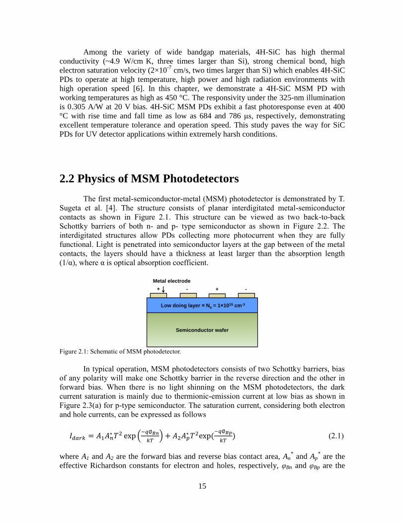
2.2 Physics of MSM Photodetectors
The first metal-semiconductor-metal (MSM) photodetector is demonstrated by T.
Sugeta et al. [4]. The structure consists of planar interdigitated metal-semiconductor
contacts as shown in Figure 2.1. This structure can be viewed as two back-to-back
Schottky barriers of both n- and p- type semiconductor as shown in Figure 2.2. The
interdigitated structures allow PDs collecting more photocurrent when they are fully
functional. Light is penetrated into semiconductor layers at the gap between of the metal
contacts, the layers should have a thickness at least larger than the absorption length
(1/α), where α is optical absorption coefficient.
Figure 2.1: Schematic of MSM photodetector.
In typical operation, MSM photodetectors consists of two Schottky barriers, bias
of any polarity will make one Schottky barrier in the reverse direction and the other in
forward bias. When there is no light shinning on the MSM photodetectors, the dark
current saturation is mainly due to thermionic-emission current at low bias as shown in
Figure 2.3(a) for p-type semiconductor. The saturation current, considering both electron
and hole currents, can be expressed as follows
𝐼𝑑𝑎𝑟 𝐴 𝐴𝑛 𝑇 (
𝑞∅
) + 𝐴 𝐴𝑝
𝑇 𝑞∅
(2.1)
where A1 and A2 are the forward bias and reverse bias contact area, An* and Ap
* are the
effective Richardson constants for electron and holes, respectively, φBn and φBp are the
Semiconductor wafer
Low doing layer ≈ Na = 1 1015 cm-3
Metal electrode
+ - + -
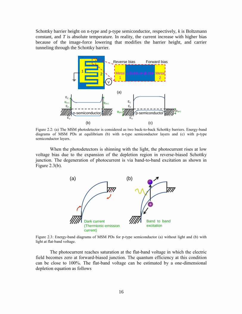
16
Schottky barrier height on n-type and p-type semiconductor, respectively, k is Boltzmann
constant, and T is absolute temperature. In reality, the current increase with higher bias
because of the image-force lowering that modifies the barrier height, and carrier
tunneling through the Schottky barrier.
Figure 2.2: (a) The MSM photodetector is considered as two back-to-back Schottky barriers. Energy-band
diagrams of MSM PDs at equilibrium (b) with n-type semiconductor layers and (c) with p-type
semiconductor layers.
When the photodetectors is shinning with the light, the photocurrent rises at low
voltage bias due to the expansion of the depletion region in reverse-biased Schottky
junction. The degeneration of photocurrent is via band-to-band excitation as shown in
Figure 2.3(b).
Figure 2.3: Energy-band diagrams of MSM PDs for p-type semiconductor (a) without light and (b) with
light at flat-band voltage.
The photocurrent reaches saturation at the flat-band voltage in which the electric
field becomes zero at forward-biased junction. The quantum efficiency at this condition
can be close to 100%. The flat-band voltage can be estimated by a one-dimensional
depletion equation as follows
Reverse bias Forward bias
Metal
1
Metal
2
p-Semiconductor
V
12
φBP1
EC
EV
EF
φBP2p-semiconductor
φBn1
EC
EV
EF
φBn2
n-semiconductor
(a)
(b) (c)
Band to band
excitation
-
+
-
+
Dark current
(Thermionic-emission
current)
(a) (b)

17
(𝑞
) (2.2)
where N is the doping concentration, εs is permittivity of semiconductor and s is the
spacing between the interdigitated fingers. The major disadvantage of the MSM
photodetectors is high dark current due to the Schottky-barrier junction rather than p-n
junction [4]. The MSM photodetectors has two primary advantages: high speed and
compatibility with CMOS technology. Conventionally, the response speed of p-n
photodiode is limited by drift time in the depletion region, diffusion of carriers, and
capacitance of the depletion region. On the other hand, the high speed operation of MSM
PDs could be attributed to the low capacitance per area of the PD due to two-dimensional
effects on a low doping thin film or semi-insulating substrate [4].
2.3 4H-SiC MSM Photodetectors
2.3.1 Fabrication Process and Characterization Methods
Figure 2.4(a) is a schematic of the 4H-SiC MSM structures used in this work. The
PDs were fabricated on p-type 3-inch research-grade 4H-SiC wafers (sheet resistivity <
2.5 Ω-cm, from Cree Inc.) with a 7-um-thick lightly p-type Al-doped epitaxial layer with
a carrier concentration of 2×10¹⁵
cm-3
. A 100-nm-thick SiO2 passivation layer was
deposited on substrate using plasma enhanced chemical vapor deposition. As shown in
Figure 2.4(b), the planar MSM PDs were defined using photolithography, e-beam
evaporation and metal lift-off process with active areas of 500 μm ×158 μm and utilized
8-μm-wide, 150-μm-long interdigitated 20 nm Cr/150 nm Pd electrodes, which have high
melting point, with 8-μm-wide spacing on the 4H-SiC substrates. This 4H-SiC MSM PD
could be fabricated with 4H-SiC JFET in the same process. Detail fabrication process
will be discussed in Chapter 3.
Figure 2.4: (a) Schematic and (b) optical image of 4H-SiC MSM PDs.
p-type 4H-SiC wafer
7 μm p-type 4H-SiC epitaxial layer
(Na = 2 1015 cm-3)
Cr/Pd electrode(a) (b)
Contact pads
Interdigitated electrodes
100 μm
SiO2

18
The crystal structure of the films was monitored with transmission electron
microscopy, TEM (JEOL JEM-2100F, operating at 200 kV). The transmission spectra
were measured with a JASCO V-670 UV-visible spectrometer in the spectral range from
250 nm to 800 nm. Photocurrent was generated under the illumination of a He–Cd laser
at a wavelength of 325 nm with laser power density of 1.02×10⁴ W/m
2. The Keithley
4200-SCS semiconductor characterization system with Tungsten probe tips were used to
measure I-V characteristics of the fabricated PDs. The time-resolved measurements were
measured by the ADLINK DAQ-2214-005 data acquisition system with Stanford
Research System SR570 low noise current preamplifier and assisted by a mechanical
chopper to switch on/off the UV light as shown in Figure 2.5. For high-temperature
characterization, the PDs are heated on hot plate and the device temperature was
monitored with calibrated thermocouple.
Figure 2.5: Schematic of time-resolved measurement system.
2.3.2 Characterization of 4H-SiC Thin Films
The cross-sectional transmission electron microscopy (TEM) image of a 7-um-
thick, lightly Al doped epitaxial 4H-SiC films and its corresponding electron diffraction
pattern are shown in Figure 2.6. There is no obvious structural defect such as micropipes
observed in the epitaxial thin films. The results suggest that the lightly doped p-type
epitaxial 4H-SiC thin films have hexagonal structure and exhibit the superior
crystallinity.
DAQ
card
He-Cd Laser
MSM
PDs
SRS low noise
preamplifier
Chopper
LabVIEW software

19
Figure 2.6: (a) Cross-sectional TEM image and (b) electron diffraction pattern of epitaxial p-type 4H-SiC
layer.
The transmission spectrum of 4H-SiC substrates is shown in Figure 2.7. The 4H-
SiC substrate shows nearly no absorption in visible/IR regions, implying that the as-
fabricated 4H-SiC MSM PDs have intrinsic visible-blindness. Based on the Tauc relation
[9], by extrapolating the linear region (red line in Figure 2.7(b)) of the (αhυ)2 versus
incident energy (hυ) plot as shown in Figure 2.7, where α is optical absorption coefficient,
h is Planck’s constant, and υ is photon frequency, the optical bandgap of 4H-SiC
substrates is approximately 3.23 eV.
Figure 2.7: The transmission spectrum (left y axis) and (αhυ)
2 (right y axis) vs. hυ plot of 4H-SiC
substrates.
2.3.3 Characterization of 4H-SiC MSM Photodetector
The I-V curves of the SiC MSM PD in the dark and under 325-nm He-Cd laser
illumination at room temperature are shown in Figure 2.8. The dark current of the 4H-SiC
MSM PD is approximately 6×10-11
A at 5 V bias which corresponds to a leakage current
density of 1.5×10⁻⁷
A/cm2. The photocurrent of PDs is approximately five orders of
magnitude larger than the dark current at 5 V bias. The responsivity (Ri) of PDs can be
obtained as follows [4]
1μm
(a)TEM preparation
(b)
2.5 3.0 3.5 4.0 4.5 5.0
0
10
20
30
40
50
60
70
Transmission
(hυ)2
Energy, hυ(eV)
Tra
nsm
issio
n (
%)
103
104
105
106
107
(h
υ)2
[(c
m-1e
V)2
]

20
(2.3)
where Iphoto is the net photocurrent and the Popt is the optical incident power, which is
4×10⁻⁴
W in our case. The calculated responsivities under the 325-nm illumination are
0.0167 A/W and 0.0305 A/W at 5 V and 20 V bias, respectively. The sensitivity factor,
photo-to-dark current ratio (PDCR), which is defined as follows [9]
(2.4)
where Id is the dark current and Ip is the photocurrent under illumination. Figure 2.9
shows the time-resolved measurements at a fixed bias of 5 V and at room temperature.
The calculated PDCR value is 1.28×10⁵ at 25 °C. The temperature-dependent response of
PDCR and responsivity shown in Figure 2.10 indicates that the 4H-SiC MSM PDs are
capable of significant UV light sensing up to 450 °C due to the low levels of dark
currents and the high thermal stability of the 4H-SiC films at high temperatures. A further
increase in temperature lowers the sensitivity factor of SiC PDs due to an increase in dark
current at a high temperature by generating the thermal carriers which cannot be
completely eliminated [9]. However, the responsivity increases as temperature increases
till 400 °C under a 5 V bias. This might be because the energy bandgap of 4H-SiC
decreases at higher temperature with the rate of 6.5×10⁻⁴
eV/K and thus boost the
photocurrent at high temperatures. Since the definition of responsivity is only counting
the photocurrent by subtracting the photocurrent by dark current, the PDCR value, further
divide by the dark current, is more suitable to express and understand the temperature
effect of the PDs.
Figure 2.8: I-V curves of the 4H-SiC MSM PDs measured in the dark and under 325-nm illumination at
room temperature.
0 5 10 15 2010
-12
10-11
10-10
10-9
10-8
10-7
10-6
10-5
10-4
Curr
en
t (A
)
Voltage (V)
Photoilluminated (λ= 325 nm)
Dark current
Photo current

21
Figure 2.9: The time dependence of the photocurrent and dark current of SiC MSM PDs at 25 °C under a 5
V bias.
To highlight the ultrafast photoresponse characteristics of the SiC PDs even at
high temperature, the time-resolved measurements were performed at a fixed bias of 5 V
and 450 °C. As shown in Figure 2.11, the current abruptly increased and then decreased
to its initial value as the light was on and off, respectively; a fully reversible response was
obtained in spite of the small PDCR value of 0.62. The shifting of the dark current at 450
°C is probably due to the thermal agitation of probe tips which is absence in the room
temperature measurement as shown in Figure 2.9. Note that the contributions of the
measured dark current are not only from the thermal carriers of MSM PDs but also from
the thermal noise of the probe tips used in the characterization set up. Suitable high-
temperature ceramic packages [10] or a high-temperature probe station can reduce the
amount of the thermal noise generated from the probe-testing and thus boost the
operating temperature for 4H-SiC MSM PDs. The set up information of the high-
temperature probe station could be found in chapter 3.
Figure 2.10: (a) PDCR value and (b) responsivity as function of temperature under a 5 V bias.
0 20 40 60 80 100-1.0x10
-6
0.0
1.0x10⁻⁶
2.0x10⁻⁶
3.0x10⁻⁶
4.0x10⁻⁶
5.0x10⁻⁶
6.0x10⁻⁶
7.0x10⁻⁶
8.0x10⁻⁶
9.0x10⁻⁶
1.0x10⁻⁵
Cu
rre
nt
(A)
Time (s)
Dark current
Photocurrent
0 100 200 300 400 50010
-1
100
101
102
103
104
105
106
PD
CR
Temperature (°C)
(a) (b)
0 100 200 300 400 5000.01
0.02
0.03
0.04
Respon
siv
ity (
A/W
)
Temperature (°C)
22
Figure 2.11: The time dependence of the photocurrent and dark current of SiC MSM PDs at 450 °C under a
5 V bias.
Figure 2.12: The transient photocurrent of SiC MSM PDs at room temperature and 400 °C under a 5 V bias.
Figure 2.12 shows the transient photocurrent of 4H-SiC MSM PDs at room
temperature and 400 °C. The operation speed of the MSM PDs can be determined by
performing the time-resolved measurement. Note that the PDCR value of time-resolved
measurement is different from the values presented in Figure 2.10. The PDCR value of
the fabricated PDs shown in figure 2.10 was measured by Keithley 4200-SCS
semiconductor characterization system which has the resolution of ~ 10-15
A. However,
the time resolution in our Keithley 4200-SCS system is only ~ 150 mS which is too big
for 4H-SiC PDs. The time-resolved measurements were then measured by custom-made
data acquisition system with Stanford Research System SR570 low noise current
preamplifier and assisted by a mechanical chopper to switch on/off the UV light. This
system has the time resolution of ~ 10 µS. Due to the unperfected ground of the
0 20 40 60 80 1001.2x10
-5
1.4x10⁻⁵
1.6x10⁻⁵
1.8x10⁻⁵
2.0x10⁻⁵
2.2x10⁻⁵
2.4x10⁻⁵
2.6x10⁻⁵
2.8x10⁻⁵
3.0x10⁻⁵
Cu
rre
nt
(A)
Time (s)
Dark current
Photocurrent
0 1 2 3 4 5 6 7 8
Cu
rre
nt
Inte
nsity
(arb
. u
nits)
Time (ms)
T = 400 °C
T = 25 °C

23
connecting cables, the current resolution of this custom-made system is only ~ 10-7
A
which makes the PDCR values are different than the one measured by Keithley system.
Therefore, the y axis in the time-resolved measurement (Fig. 4(b)) is labeled as arbitrary
units. The quantitative parameters of describing how fast the photodetector responds to
external light illumination are rise time and fall time. The rise time is the time required
reaching the steady-state photocurrent and is defined as the time difference between 10%
and 90% of photocurrent. Fall time means the time required for the decay when the
optical excitation is interrupted and is the time difference between 90% and 10% of
photocurrent [11]. Extracted rise time and fall time are summarized and listed on Table 1.
Rise time and fall time of PD at room temperature are 594 and 699 μs, respectively. As
temperature increases to 400 °C, the rise time and the fall time are increased to 684 and
786 μs, respectively, indicating that temperature-tolerant photoresponse of SiC MSM
PDs. Due to the unperfected ground problem of time-resolved measurement system, the
rise and fall time of 4H-SiC MSM PDs are slightly underestimated. The reason for the
decrease in the operation speed of PDs with temperature is stated as follows. The transit-
time-limited bandwidth is proportional to the saturation velocity at fixed spacing between
fingers [12]
𝑟
√
(2.5)
where ftr is the transit-time-limited 3-dB bandwidth, vs is the saturation velocity, and s is
the spacing between electrode fingers. The hole/electron saturation velocity of 4H-SiC is
decreased as temperature increases [13], leading to the decrease in the bandwidth and
thus the speed of the PD at a high temperature.
Temperature (°C) Rise Time (μs) Fall Time (μs)
25 594 699
400 684 786
Table 2.1: Response time of fabricated 4H-SiC MSM photodetectors.
2.4 Antireflection Layer Using Nanostructure
The responsivity of 0.0305 A/W at 20 V and under 325-nm illumination is
comparable with the commercial SiC UV detector chip fabricated by Cree Inc. (~0.056
A/W) at room temperature [2]. For high temperature characterization, there are several
works reporting the PDCR value of approximately 2, 2.5, 7.5 by using amorphous SiCN
[14], SiCBN [3], nanocrystalline SiC [9] at 200 °C, respectively. The PDCR value of 375
at 200 °C of this work is superior to the previous works. In order to further boost the
responsivity and PDCR value of 4H-SiC MSM PDs, antireflection coating can be added
on PDs by reducing the surface reflection and allowing more light to reach the active
region. A conventional single layer antireflection coating (ARC) works only in a limited
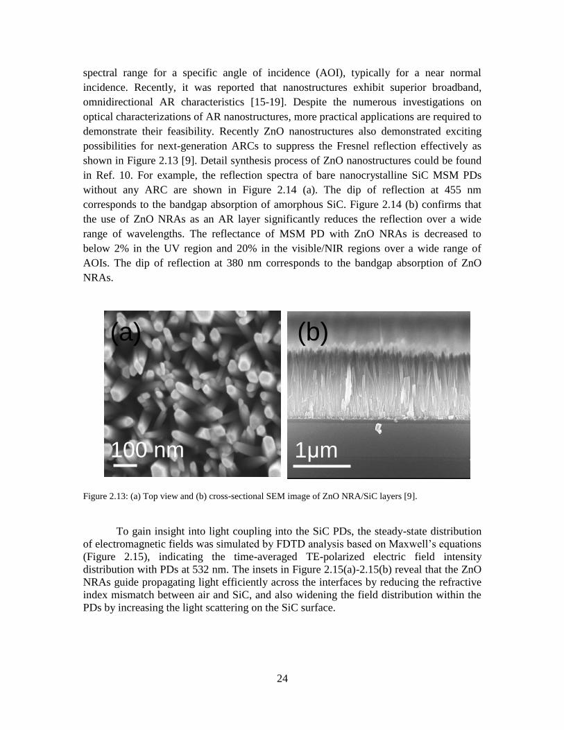
24
spectral range for a specific angle of incidence (AOI), typically for a near normal
incidence. Recently, it was reported that nanostructures exhibit superior broadband,
omnidirectional AR characteristics [15-19]. Despite the numerous investigations on
optical characterizations of AR nanostructures, more practical applications are required to
demonstrate their feasibility. Recently ZnO nanostructures also demonstrated exciting
possibilities for next-generation ARCs to suppress the Fresnel reflection effectively as
shown in Figure 2.13 [9]. Detail synthesis process of ZnO nanostructures could be found
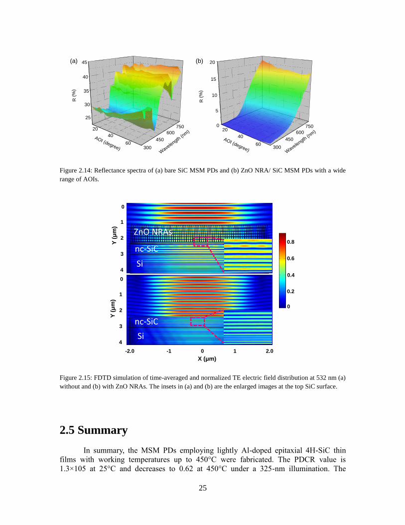
in Ref. 10. For example, the reflection spectra of bare nanocrystalline SiC MSM PDs
without any ARC are shown in Figure 2.14 (a). The dip of reflection at 455 nm
corresponds to the bandgap absorption of amorphous SiC. Figure 2.14 (b) confirms that
the use of ZnO NRAs as an AR layer significantly reduces the reflection over a wide
range of wavelengths. The reflectance of MSM PD with ZnO NRAs is decreased to
below 2% in the UV region and 20% in the visible/NIR regions over a wide range of
AOIs. The dip of reflection at 380 nm corresponds to the bandgap absorption of ZnO
NRAs.
Figure 2.13: (a) Top view and (b) cross-sectional SEM image of ZnO NRA/SiC layers [9].
To gain insight into light coupling into the SiC PDs, the steady-state distribution
of electromagnetic fields was simulated by FDTD analysis based on Maxwell’s equations
(Figure 2.15), indicating the time-averaged TE-polarized electric field intensity
distribution with PDs at 532 nm. The insets in Figure 2.15(a)-2.15(b) reveal that the ZnO
NRAs guide propagating light efficiently across the interfaces by reducing the refractive
index mismatch between air and SiC, and also widening the field distribution within the
PDs by increasing the light scattering on the SiC surface.
100 nm 1μm
(a) (b)
25
Figure 2.14: Reflectance spectra of (a) bare SiC MSM PDs and (b) ZnO NRA/ SiC MSM PDs with a wide
range of AOIs.
Figure 2.15: FDTD simulation of time-averaged and normalized TE electric field distribution at 532 nm (a)
without and (b) with ZnO NRAs. The insets in (a) and (b) are the enlarged images at the top SiC surface.
2.5 Summary
In summary, the MSM PDs employing lightly Al-doped epitaxial 4H-SiC thin
films with working temperatures up to 450°C were fabricated. The PDCR value is
1.3×10⁵ at 25°C and decreases to 0.62 at 450°C under a 325-nm illumination. The
20
40
60
25
30
35
40
45
300
450
600
750
R (
%)
Wave
length (n
m)
AOI (degree)
20
40
60
0
5
10
15
20
300
450
600
750
R (
%)
Wave
length (n
m)
AOI (degree)
(a) (b)
0
1
2
3
4
Y (μ
m)
nc-SiC
Si
ZnO NRAs
-2.0 -1 0 1 2.0
X (μm)
0
0.2
0.4
0.6
0.8
nc-SiC
Si
0
1
2
3
4
Y (μ
m)

26
responsivity is 0.0305 A/W at 20 V bias under the 325-nm illumination. Moreover, the
operation speed of PDs exhibits temperature-tolerant characteristics; as the temperature
increased from 25°C and 400°C, the rise time and the fall time of the PD increase from
594 to 684 μs and from 699 to 786 μs, respectively. This work demonstrates that the 4H-
SiC holds promise for the next-generation visible-/IR-blind UV PDs for use in extremely
harsh environments.
2.6 References [1] W.-R. Chang, Y.-K. Fang, S.-F. Ting, Y.-S. Tsair, C.-N. Chang, C.-Y. Lin, and S.-
F. Chen, "The hetero-epitaxial SiCN/Si MSM photodetector for high-temperature
deep-UV detecting applications," IEEE Electron Device Letters,, vol. 24, pp. 565-
567, 2003.
[2] E. Monroy, F. Omnes, and F. Calle, "Wide-bandgap semiconductor ultraviolet
photodetectors," Semiconductor Science and Technology, vol. 18, pp. R33-R51,
Apr 2003.
[3] A. Vijayakumar, K. Sundaram, and R. Todi, "Amorphous-SiCBN-based metal–
semiconductor–metal photodetector for high-temperature applications," IEEE
Electron Device Letters, vol. 28, pp. 713-715, 2007.
[4] S. M. Sze and K. K. NG, Physics of semiconductor devices: Wiley, 2007.
[5] D. M. Brown, E. T. Downey, M. Ghezzo, J. W. Kretchmer, R. J. Saia, Y. S. Liu, J.
A. Edmond, G. Gati, J. M. Pimbley, and W. E. Schneider, "Silicon carbide UV
photodiodes," IEEE Transactions on Electron Devices, vol. 40, pp. 325-333,
1993.
[6] A. A. Stephen E. Saddow, Advances in Silicon Carbide Processing and
Applications, 2004.
[7] S. Assefa, F. N. Xia, S. W. Bedell, Y. Zhang, T. Topuria, P. M. Rice, and Y. A.
Vlasov, "CMOS-integrated high-speed MSM germanium waveguide
photodetector," Optics Express, vol. 18, pp. 4986-4999, Mar.
[8] D.-S. Tsai, C.-A. Lin, W.-C. Lien, H.-C. Chang, Y.-L. Wang, and J.-H. He, "Ultra-
High-Responsivity Broadband Detection of Si Metal–Semiconductor–Metal
Schottky Photodetectors Improved by ZnO Nanorod Arrays," ACS nano, vol. 5,
pp. 7748-7753, 2011.
[9] W. C. Lien, D. S. Tsai, S. H. Chiu, D. G. Senesky, R. Maboudian, A. P. Pisano,
and J. H. He, "Low-Temperature, Ion Beam-Assisted SiC Thin Films With
Antireflective ZnO Nanorod Arrays for High-Temperature Photodetection," IEEE
Electron Device Letters, vol. 32, pp. 1564-1566, Nov 2011.
[10] P. G. Neudeck, S. L. Garverick, D. J. Spry, L. Y. Chen, G. M. Beheim, M. J.
Krasowski, and M. Mehregany, "Extreme temperature 6H-SiC JFET integrated
circuit technology," Physica Status Solidi A-Applications and Materials Science,
vol. 206, pp. 2329-2345, Oct 2009.
[11] K. Wang, F. Chen, N. Allec, and K. S. Karim, "Fast Lateral Amorphous-Selenium
Metal-Semiconductor-Metal Photodetector With High Blue-to-Ultraviolet

27
Responsivity," IEEE Transactions on Electron Devices, vol. 57, pp. 1953-1958,
Aug.
[12] J. Kim, W. B. Johnson, S. Kanakaraju, L. C. Calhoun, and C. H. Lee,
"Improvement of dark current using InP/InGaAsP transition layer in large-area
InGaAs MSM photodetectors," IEEE Transactions on Electron Devices, vol. 51,
pp. 351-356, Mar 2004.
[13] S. Potbhare, N. Goldsman, A. Lelis, J. M. McGarrity, F. B. McLean, and D.
Habersat, "A physical model of high temperature 4H-SiC MOSFETs," IEEE
Transactions on Electron Devices, vol. 55, pp. 2029-2040, Aug 2008.
[14] W. R. Chang, Y. K. Fang, S. F. Ting, Y. S. Tsair, C. N. Chang, C. Y. Lin, and S. F.
Chen, "The hetero-epitaxial SiCN/Si MSM photodetector for high-temperature
deep-UV detecting applications," IEEE Electron Device Letters, vol. 24, pp. 565-
567, Sep 2003.
[15] J. Huang, X. Wang, and Z. L. Wang, "Bio-inspired fabrication of antireflection
nanostructures by replicating fly eyes," Nanotechnology, vol. 19, p. 025602, 2008.
[16] Y.-C. Chao, C.-Y. Chen, C.-A. Lin, Y.-A. Dai, and J.-H. He, "Antireflection effect
of ZnO nanorod arrays," Journal of Materials Chemistry, vol. 20, pp. 8134-8138,
2010.
[17] Y.-A. Dai, H.-C. Chang, K.-Y. Lai, C.-A. Lin, R.-J. Chung, G.-R. Lin, and J.-H.
He, "Subwavelength Si nanowire arrays for self-cleaning antireflection coatings,"
Journal of Materials Chemistry, vol. 20, pp. 10924-10930, 2010.
[18] Y.-L. Chueh, Z. Fan, K. Takei, H. Ko, R. Kapadia, A. A. Rathore, N. Miller, K.
Yu, M. Wu, and E. Haller, "Black Ge based on crystalline/amorphous core/shell
nanoneedle arrays," Nano letters, vol. 10, pp. 520-523, 2009.
[19] G. Lin, K. Lai, C. Lin, Y. Lai, and J. He, "Efficiency enhancement of InGaN-
based multiple quantum well solar cells employing antireflective ZnO nanorod
arrays," IEEE Electron Device Letters, vol. 32, pp. 1104-1106, 2011.

28
Chapter 3
Silicon Carbide N-Channel Raised Gate
Junction Field-Effect Transistors
3.1 Introduction
High temperature sensors and electronics that operate at 300-600 °C are required
for in-situ monitoring of fuel combustion, subsurface reservoirs (deep well drilling), and
Venus and Jupiter surface exploration [1-4]. The sensors and electronics capable of high-
temperature operation not only minimize the expensive and large cooling systems, but
also improve the reliability of the system [5]. Silicon carbide has become the candidate
for these harsh environment sensing applications because of its wide bandgap (3.2 eV for
4H-SiC), excellent chemical and thermal stability, and high breakdown electric field
strength (5 MV/cm) [4]. Operational amplifiers (Opamps) are the main elements of
complex integrated circuits. SiC-based opamps have been investigated based on the
MOSFET and JFET device structures [6-8]. While MOSFETs suffer from the low
inversion mobility and poor gate oxide reliability, which limit the operating temperature
to 400 °C [7-9], transistors utilizing SiC pn junctions (JFET and BJT) enable increased
operation durations at high temperature [10-12]. BJTs exhibit superior electrical
properties, but require higher power consumption and rapidly degraded at temperature
above 350 °C, and more studies on long time stability are needed [13]. Currently, most
SiC JFETs for low voltage analog signal amplification utilize 6H-SiC and show long
term reliability more than 5000 hours of continuous 500 °C electrical operation in air [6].
However, replacing 6H-SiC with 4H-SiC substrates has attracted attention recently,
because 4H-SiC has a larger bandgap, higher electron mobility than 6H-SiC (950 cm2/Vs
perpendicular to c-axis and 1150 cm2/Vs parallel to c-axis) and has commercially
available wafers up to 6 inches [14, 15]. In this chapter, we develop the low voltage,
normally-on, lateral JFETs using 4H-SiC and characterize their electrical properties from
room temperature up to 600 °C in air.
3.2 Physics of JFET

29
The junction field-effect transistor was invented by W. Shockley in 1952 [16].
The gate voltage changes the pn junction depletion width and electric field in the
direction normal to the semiconductor surface. It is a unipolar transistor which means
only one type of carrier is involved in the operation. Using the pn junction to control the
associated electric field and conducting current with majority carriers offers the
advantage of using a JFET for high temperature applications, as it eliminates the chance
of metal-semiconductor-oxide interface traps, increase oxide reliability, and reduces the
minority carrier instability [5].
The fundamental operation principle of n-channel JFET is described as follows
[11, 16, 17]. First, the gate terminal is grounded and the drain voltage is 0 V. JFET is in
thermal equilibrium. As shown in Figure 3.1 (a), once the p+-n junction is deposited, the
depletion width is formed. Due to the heavily doped p-type gate area, the depletion region
primarily extends into the lightly doped n-channel area of the device. The device at this
stage is in off state (Figure 3.1 (b)). Applying VD to small positive voltages, the channel
is formed at the non-depleted and current-carrying region as shown in Figure 3.1 (c). The
channel acts like a simple resistor, and the drain current is increased linearly with drain
voltage as shown in point B of Figure 3.1 (d). As VD keeps increasing, the depletion
width around drain side is widened as shown in Figure 3.1 (e). The channel region is still
like a resistor, but because of the loss of the conduction channel near the drain side, the
resistance between the source and drain is increased and the increasing rate of ID is
reduced which results the slope of ID-VD characteristic decreases at larger VD as shown in
point C of Figure 3.1 (f). If we continue to increase the VD, the channel is further
narrowed and eventually reaches the pinch-off state shown in Figure 3.1 (g). The slope of
ID-VD characteristic is approximately zero at the pinch-off set, as shown at point D in
Figure 3.1 (h), and the drain bias at this point is called saturation drain voltage (VDsat). As
the drain voltage becomes larger than VDsat, the pinch-off area widens to the extent of ΔL.
The voltage difference between VD and VDsat is mainly dropped along the ΔL, and the
major mechanism of current flow is through drift current as shown in Figure 3.1 (i). The
corresponding ID-VD characteristic saturates, namely remaining constant at the saturation
drain current shown in point E of Figure 3.1 (j).
The drain current (IDS) versus drain-to-source voltage (VDS) characteristics of
JFET can be expressed using the conventional 3/2 power model which originally
developed for long channel Si JFET [5, 17]. The basic assumptions are uniformly doped
channel with gradual-channel approximation (i.e., electric field perpendicular to channel
is smaller than electric field parallel to channel), abrupt depletion layer, small gate
leakage current and constant mobility. Assuming that the Fermi level on the heavily
doped side is positioned at the band edge, the built-in potential (Vbi) of p+-n junction is
given by
𝑞[ 𝑇 (
𝑛 )] (3.1)
where q is unit electronic charge, Eg is bandgap of semiconductor, k is Boltzmann
constant, T is temperature, ND+ is ionized donor impurity concentration, and ni is intrinsic
carrier concentration. The pinch-off potential (VP) is given by

30
𝑞
(3.2)
where D is the channel depth and εs is permittivity of 4H-SiC. The normalized pinch-off
current (IP′) is given by
𝐼 (
𝑞 𝑛
) (3.3)
where n is ionized carrier concentration in the channel and µn is mobility of carriers. The
gate threshold voltage (VT) around which the JFET is turned on and off is given by
(3.4)
In triode region, where VDS < VDsat = VGS - VT, the drain current is given by
𝐼 (
) 𝐼
[
[{
}
{
}
]] + (3.5)
In saturation region, where VDS ≥ VDsat = VGS - VT,
𝐼 (
) 𝐼
[ (
) + (
)
] + (3.6)
where W and L are channel width and length, respectively, VGS is the gate-to-source
voltage, and λ is channel length modulation parameter of the JFET.

31
Figure 3.1: Visualization of various phases of JFET operation and the corresponding ID-VD characteristics
at VGS = 0 V. Note the SiC substrate serves as the body biasing point. The blue color in schematic
represents the depletion regions, and the yellow color shows the channel region. The shape of the channel is
for the purpose of demonstration and it is not the real situation.
SiC substrate
n epi
Drain
n+
Gate
p+
A. Off vDS
ID
Source
n+
SiC substrate
n epi
Drain
n+
Gate
p+
B
A. Off vDS
iD
+
Source
n+
(a) (b)
(c) (d)
SiC substrate
n epi
Drain
n+
Gate
p+
Triode
B
A. Off
C
vDS
iD
+ +
Source
n+
SiC substrate
n epi
Gate
p+
Triode
B
A. Off
C D
vDS
iD
+ +
+
Source
n+
(e) (f)
(g) (h)
SiC substrate
n epi
Gate
p+
Triode Saturation
B
A. Off
CD E
vDS
iD
+ +
+ +
vGS = 0
vGS
Source
n+
(i) (j)
Drain
n+
Drain
n+

32
3.3 Fabrication Process
Figure 3.2 is a cross-sectional schematic of a lateral n-channel raised gate 4H-SiC
JFET used in this work. The device structure is similar to that work of the NASA Glenn
Research Center except the material is changed to 4H-SiC [18]. The transistor consists of
p-type 4H-SiC wafer (from Cree Inc.) with three epitaxial layers (from Ascatron AB). A
5 µm p- epitaxial layer with doping concentration of 2×10¹⁵
cm-3
, followed by 300 nm n-
epitaxial layer with doping concentration of 1×10¹⁷
cm-3
and 200 nm p+ epitaxial layer
with doping concentration of 2×10¹⁹
cm-3
were grown on the p-type wafer with the
resistivity of approximately 1 Ω-cm. The p+ epitaxial layer served as the gate and n
epitaxial layer is used for the channel of JFET. The entire fabrication process flow is
shown in Figure 3.3 including seven lithography masks. First, the p+ gate was time etched
using transformer coupled plasma (TCP) etcher with 90 sccm Cl2 and 10 sccm BCl3
under RF bias of 150 W. 1 μm plasma-enhanced chemical vapor deposition (PECVD)
SiO2 was patterned to define the source and drain area with nitrogen implantation at 600
˚C which facilitates Ohmic contact to the metal with reduced damage of crystallinity [19].
Figure 3.2: Schematic of a lateral n-channel raised gate 4H-SiC JFET.
4H-SiC Substrate
p- 4H-SiC
n 4H-SiC
p+
350 µm
7 µm
300 nm
200 nm
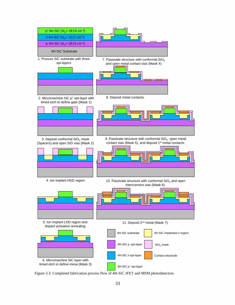
33
Figure 3.3: Completed fabrication process flow of 4H-SiC JFET and MSM photodetectors.
4H-SiC substrate
4H-SiC p- epi-layer
4H-SiC n epi-layer
4H-SiC p+ epi-layer
SiO2 mask
4H-SiC implanted n region
Contact electrode
4H-SiC Substrate
p- 4H-SiC (NA= 2E15 cm-3)
n 4H-SiC (ND= 1E17 cm-3)
p+ 4H-SiC (NA= 2E19 cm-3)
1. Procure SiC substrate with three
epi-layers
8. Deposit metal contacts.2. Micromachine SiC p+ epi-layer with
timed etch to define gate (Mask 1)
3. Deposit conformal SiO2 mask
(Spacers) and open S/D vias (Mask 2)
4. Ion implant HDD region
6. Micromachine SiC layer with
timed etch to define mesa (Mask 3)
5. Ion implant LDD region and
dopant activation annealing
7. Passivate structure with conformal SiO2
and open metal contact vias (Mask 4)
9. Passivate structure with conformal SiO2, open metal
contact vias (Mask 5), and deposit 1st metal contacts.
10. Passivate structure with conformal SiO2 and open
interconnect vias (Mask 6).
11. Deposit 2nd metal (Mask 7).

34
The implantation of a box profile was formed using 1.4×10¹⁵
, 7×10¹⁴
, and
3.6×10¹⁴
doses at 60, 40, and 20 keV energies, respectively. An example of SiC
insulated-gate bipolar transistor (IGBT) of TCAD Sentaurus process simulation has been
modified for predicting the dopants concentration distribution and depth profile. The
simulation of ion implantation uses the stopping and range of ions in matter (SRIM)
which is based on the Monte Carlo simulation method. Based on this simulation, the
implantation yields a nitrogen concentration higher than 1019
cm-3
as shown in Figure 3.4.
After ion implantation, the oxide layers were removed by the buffer oxide etching
solution (hydrofluoric acid). The second lighter-dose nitrogen was implanted using
3.2×10¹²
, 8×10¹¹
, 8×10¹¹
, and 1×10¹²
doses at 33, 24, 18, and 10 keV energies,
respectively [18].
Figure 3.4: Simulated doping profile of heavily doped drain and source region.
The implanted dopants were electrically activated by annealing samples capped
with 2 µm PECVD SiO2 at 1450 °C under an Argon atmosphere for 30 minutes. Figure
3.5 (a) shows the cross-sectional scanning TEM image of the implanted area after
annealing. Electron diffraction of the implanted area suggests that the implanted area can
be restored back to single crystal after high temperature annealing as shown in Figure 3.5
(b). Figure 3.6 shows the atomic force microscope (AFM) images of SiC sample before
and after annealing. The root-mean-square (RMS) roughness is slightly increased from
0.366 nm to 2.65 nm which could be attributed to combination of Si outdiffusion due to
the strain created by the ion-implantation damage and non uniform thermal oxidation of
SiC surface at high temperature [20].
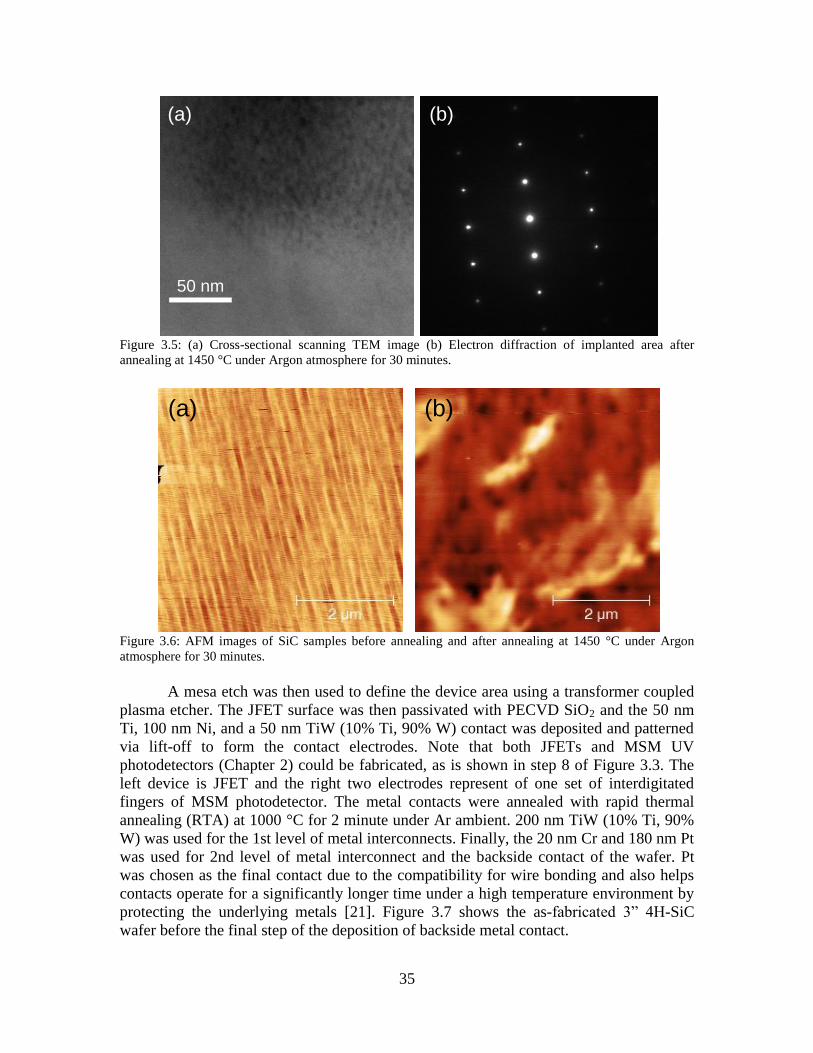
35
Figure 3.5: (a) Cross-sectional scanning TEM image (b) Electron diffraction of implanted area after
annealing at 1450 °C under Argon atmosphere for 30 minutes.
Figure 3.6: AFM images of SiC samples before annealing and after annealing at 1450 °C under Argon
atmosphere for 30 minutes.
A mesa etch was then used to define the device area using a transformer coupled
plasma etcher. The JFET surface was then passivated with PECVD SiO2 and the 50 nm
Ti, 100 nm Ni, and a 50 nm TiW (10% Ti, 90% W) contact was deposited and patterned
via lift-off to form the contact electrodes. Note that both JFETs and MSM UV
photodetectors (Chapter 2) could be fabricated, as is shown in step 8 of Figure 3.3. The
left device is JFET and the right two electrodes represent of one set of interdigitated
fingers of MSM photodetector. The metal contacts were annealed with rapid thermal
annealing (RTA) at 1000 °C for 2 minute under Ar ambient. 200 nm TiW (10% Ti, 90%
W) was used for the 1st level of metal interconnects. Finally, the 20 nm Cr and 180 nm Pt
was used for 2nd level of metal interconnect and the backside contact of the wafer. Pt
was chosen as the final contact due to the compatibility for wire bonding and also helps
contacts operate for a significantly longer time under a high temperature environment by
protecting the underlying metals [21]. Figure 3.7 shows the as-fabricated 3” 4H-SiC
wafer before the final step of the deposition of backside metal contact.
50 nm
(a) (b)
(a) (b)

36
Figure 3.7: Fabricated 3” 4H-SiC wafer.
Devices were characterized on a hot chuck of high temperature probe station
(Signatone Inc.) as shown in Figure 3.8. This high temperature probe station consists of
ceramic hot chunk, thermal heater, and water cooler, and the chunk temperature goes up
to 600 °C with low thermal noise of 10-9
-10-8
A at 600 °C. An HP 4156B semiconductor
parameter analyzer and Agilent B2912A precision source/measurement unit with
tungsten probe tips were used to measure the I-V characteristics of the devices as shown
in Figure 3.9.
Figure 3.8: High temperature probe station.
Thermal heater
Water cooler
Ceramic hot chunk
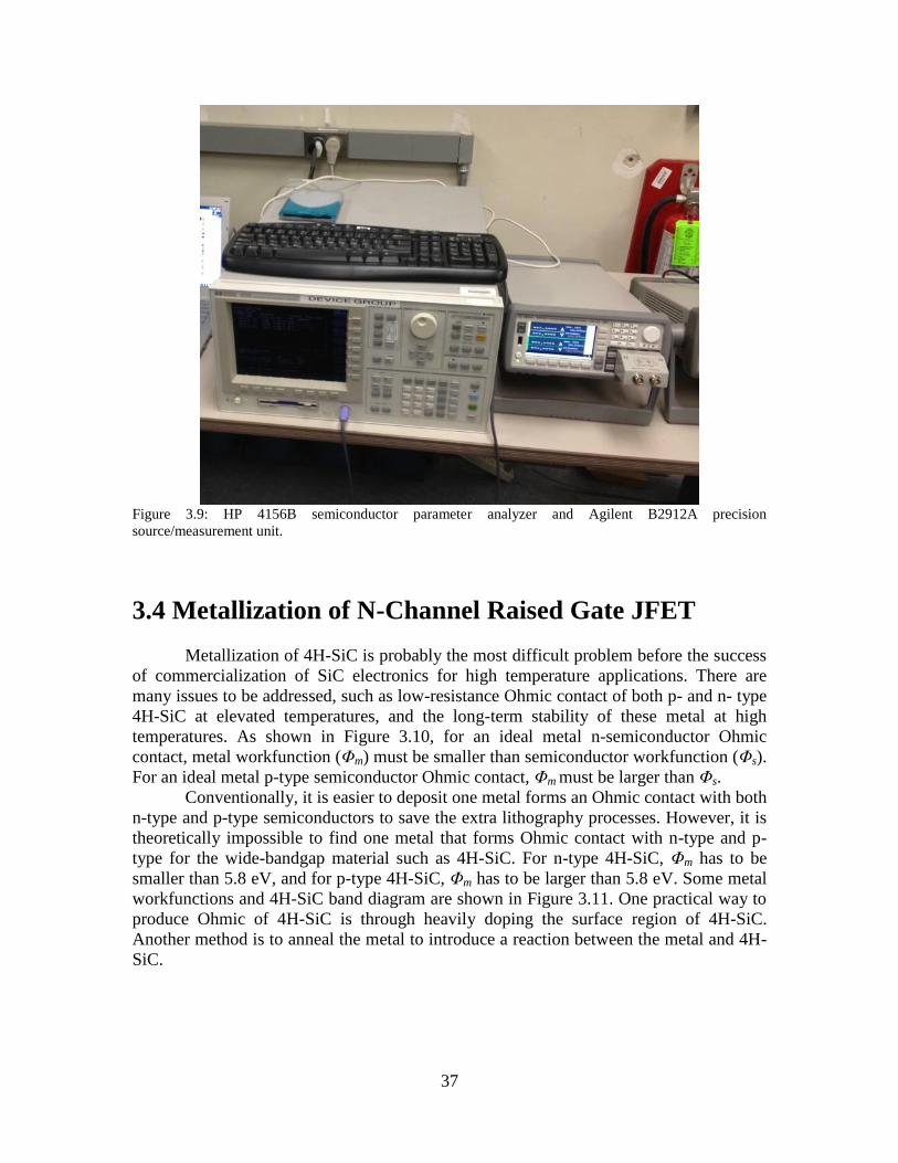
37
Figure 3.9: HP 4156B semiconductor parameter analyzer and Agilent B2912A precision
source/measurement unit.
3.4 Metallization of N-Channel Raised Gate JFET
Metallization of 4H-SiC is probably the most difficult problem before the success
of commercialization of SiC electronics for high temperature applications. There are
many issues to be addressed, such as low-resistance Ohmic contact of both p- and n- type
4H-SiC at elevated temperatures, and the long-term stability of these metal at high
temperatures. As shown in Figure 3.10, for an ideal metal n-semiconductor Ohmic
contact, metal workfunction (Φm) must be smaller than semiconductor workfunction (Φs).
For an ideal metal p-type semiconductor Ohmic contact, Φm must be larger than Φs.
Conventionally, it is easier to deposit one metal forms an Ohmic contact with both
n-type and p-type semiconductors to save the extra lithography processes. However, it is
theoretically impossible to find one metal that forms Ohmic contact with n-type and p-
type for the wide-bandgap material such as 4H-SiC. For n-type 4H-SiC, Φm has to be
smaller than 5.8 eV, and for p-type 4H-SiC, Φm has to be larger than 5.8 eV. Some metal
workfunctions and 4H-SiC band diagram are shown in Figure 3.11. One practical way to
produce Ohmic of 4H-SiC is through heavily doping the surface region of 4H-SiC.
Another method is to anneal the metal to introduce a reaction between the metal and 4H-
SiC.
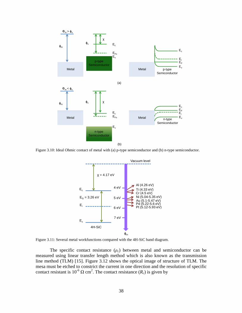
38
Figure 3.10: Ideal Ohmic contact of metal with (a) p-type semiconductor and (b) n-type semiconductor.
Figure 3.11: Several metal workfunctions compared with the 4H-SiC band diagram.
The specific contact resistance (ρc) between metal and semiconductor can be
measured using linear transfer length method which is also known as the transmission
line method (TLM) [15]. Figure 3.12 shows the optical image of structure of TLM. The
mesa must be etched to constrict the current in one direction and the resolution of specific
contact resistant is 10-6
Ω cm2. The contact resistance (Rc) is given by
Φm > ϕs
ϕm
ϕs
χ
Ev
EFs
Ec
p-type
Semiconductor
Metal
Φm < ϕs
ϕmϕs χ
Ev
EFs
Ec
n-type
Semiconductor
Metal
Metal
Metal
(a)
(b)
Ev
EF
Ec
Ei
p-type
Semiconductor
n-type
Semiconductor
Ev
EF
Ec
Ei
7 eV
5 eV
χ = 4.17 eV
EG = 3.26 eV
Ec
Ev
Ei
4H-SiC
4 eV
6 eV
Vacuum level
Al (4.26 eV)
Ti (4.33 eV) Cr (4.5 eV) Ni (5.04-5.35 eV) Au (5.1-5.47 eV) Pd (5.22-5.6 eV) Pt (5.12-5.93 eV)
ϕm

39
√
(3.7)
where ρc is the specific contact resistance between metal and semiconductor (Ω cm2), Rsh
is the sheet resistance of the semiconductor (Ω/□), and W is the width of the contact. The
sheet resistance is given by
𝑞 𝑛 (3.8)
The Rsh and ρc can be estimated by measuring resistance between contacts with variable
distances (d), namely the TLM shown in Figure 3.12, using the following equation,
+
√
(3.9)
Figure 3.12: Optical image of TLM structure.
In order to simplify the fabrication process of the first generation of raised gate
4H-SiC JFET, one metal stack of 50 nm Ti/100 nm Ni/ 50 nm TiW was chosen for the
contact electrodes for both p+ gate and n
+ source/drain areas. Ti acts as an adhesion layer,
Ni is the main contact electrode, and TiW acts as a capping layer which has a high
melting point and has been proven to have long term stability after high temperature
exposure of 500 °C [22]. Figure 3.13 shows the current-voltage (I-V) measurement of
metal and n-type 4H-SiC for TLM structure. The contact is a Schottky contact before
RTA and it becomes Ohmic contact after the RTA.
d= 5 µm 10 µm 20 µm 40 µm 80 µm
W
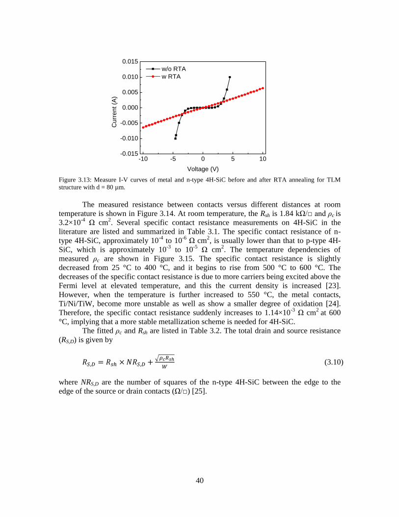
40
Figure 3.13: Measure I-V curves of metal and n-type 4H-SiC before and after RTA annealing for TLM
structure with d = 80 µm.
The measured resistance between contacts versus different distances at room
temperature is shown in Figure 3.14. At room temperature, the Rsh is 1.84 kΩ/□ and ρc is
3.2×10⁻⁴
Ω cm2. Several specific contact resistance measurements on 4H-SiC in the
literature are listed and summarized in Table 3.1. The specific contact resistance of n-
type 4H-SiC, approximately 10-4
to 10-6
Ω cm2, is usually lower than that to p-type 4H-
SiC, which is approximately 10-3
to 10-5
Ω cm2. The temperature dependencies of
measured ρc are shown in Figure 3.15. The specific contact resistance is slightly
decreased from 25 °C to 400 °C, and it begins to rise from 500 °C to 600 °C. The
decreases of the specific contact resistance is due to more carriers being excited above the
Fermi level at elevated temperature, and this the current density is increased [23].
However, when the temperature is further increased to 550 °C, the metal contacts,
Ti/Ni/TiW, become more unstable as well as show a smaller degree of oxidation [24].
Therefore, the specific contact resistance suddenly increases to 1.14×10⁻³
Ω cm2
at 600
°C, implying that a more stable metallization scheme is needed for 4H-SiC.
The fitted ρc and Rsh are listed in Table 3.2. The total drain and source resistance
(RS,D) is given by
+√
(3.10)
where NRS,D are the number of squares of the n-type 4H-SiC between the edge to the
edge of the source or drain contacts (Ω/□) [25].
-10 -5 0 5 10-0.015
-0.010
-0.005
0.000
0.005
0.010
0.015
Cu
rre
nt
(A)
Voltage (V)
w/o RTA
w RTA

41
Figure 3.14: Measured resistance between contacts vs. different distances at room temperature of
Ti/Ni/TiW metal stacks and n-type 4H-SiC.
Poly type Metals Doping (cm-3
) ρc( Ω cm2) Ref
n Ni-Cr 1.3×10¹⁹
1.2×10⁻⁵
[26]
n TiC 1.3×10¹⁹
4×10⁻⁵
[27]
n Ni 1×10¹⁹
6×10⁻⁶
[28]
n TiW (30:70) 1.3×10¹⁹
1.2×10⁻⁴
[22]
n W-Ni (50:50) 2×10¹⁹
5.81×10⁻⁴
[29]
p TiC 1×10²⁰
6×10⁻⁵
[27]
p Ni 1×10²¹
1.5×10⁻⁴
[28]
p TiW (30:70) 6×10¹⁸
1.2×10⁻⁴
[22]
p Ge/Ti/Al 4.5×10¹⁸
1.03×10⁻⁴
[30]
p Al-Si-Ti 3-5×10¹⁹
9.6×10⁻⁵
[31]
p Ni/Ti/Al/Ni 3-4×10¹⁹
1.5×10⁻⁵
[32]
Table 3.1: Specific contact resistance measurements on 4H-SiC in the literature.
0 10 20 30 40 50 60 70 80 90 100
200
400
600
800
1000
1200
1400
1600
1800
Re
sis
tan
ce
(
)
d (m)
25 C

42
Figure 3.15: Temperature dependences of specific contact resistance of Ti/Ni/TiW metal stacks to n
+ 4H-
SiC.
Temperature (°C) Rsh (kΩ/□) ρc (Ω cm2)
25 1.842 3.22×10⁻⁴
110 1.700 2.72×10⁻⁴
210 1.666 2.24×10⁻⁴
300 1.660 1.97×10⁻⁴
400 1.664 1.74×10⁻⁴
500 1.627 2.02×10⁻⁴
550 1.378 5.26×10⁻⁴
600 1.090 1.136×10⁻³
Table 3.2: Sheet resistance and specific contact resistance of Ti/Ni/TiW metal stacks and n-type 4H-SiC at
different temperatures.
Figure 3.16 shows the I-V measurement of metal and p+ gate of 4H-SiC for the
TLM structure. The contact is still Schottky in nature after the RTA except the current
intensity is increased. There is one study that reported the 50 nm Ti/ 100 nm Ni is able to
form an Ohmic contact with both n- and p-type 4H-SiC after RTA [33]. In our case, it
only works for the n-type 4H-SiC. However, a non ideal or semi-rectifying contact to
JFET’s gate region is still acceptable for the JFET operation [5].
0 100 200 300 400 500 6000.0
2.0x10⁻⁴
4.0x10⁻⁴
6.0x10⁻⁴
8.0x10⁻⁴
1.0x10⁻³
1.2x10⁻³
1.4x10⁻³
c (
cm
2)
Temperature (C)
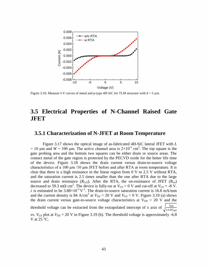
43
Figure 3.16: Measure I-V curves of metal and p-type 4H-SiC for TLM structure with d = 5 µm.
3.5 Electrical Properties of N-Channel Raised Gate
JFET
3.5.1 Characterization of N-JFET at Room Temperature
Figure 3.17 shows the optical image of as-fabricated 4H-SiC lateral JFET with L
= 10 μm and W = 100 μm. The active channel area is 2×10⁻⁵
cm2. The top square is the
gate probing area and the bottom two squares can be either drain or source areas. The
contact metal of the gate region is protected by the PECVD oxide for the better life time
of the device. Figure 3.18 shows the drain current versus drain-to-source voltage
characteristics of a 100 μm /10 μm JFET before and after RTA at room temperature. It is
clear that there is a high resistance in the linear region from 0 V to 2.5 V without RTA,
and the saturation current is 2.5 times smaller than the one after RTA due to the large
source and drain resistance (RS,D). After the RTA, the on-resistance of JFET (Ron)
decreased to 59.3 mΩ cm2. The device is fully-on at VGS = 0 V and cut-off at VGS = -8 V.
λ is estimated to be 3.88×10⁻³
V-1
. The drain-to-source saturation current is 16.8 mA/mm
and the current density is 84 A/cm2 at VDS = 20 V and VGS = 0 V. Figure 3.19 (a) shows
the drain current versus gate-to-source voltage characteristics at VDS = 20 V and the
threshold voltage can be extracted from the extrapolated intercept of x axis of √
vs. VGS plot at VDS = 20 V in Figure 3.19 (b). The threshold voltage is approximately -6.8
V at 25 °C.
-10 -5 0 5 10-0.008
-0.006
-0.004
-0.002
0.000
0.002
0.004
0.006
0.008
Cu
rre
nt
(A)
Voltage (V)
w/o RTA
w RTA

44
Figure 3.17: Optical image of a n-channel raised gate 4H-SiC JFET with L = 10 μm and W = 100 μm.
Figure 3.18: IDS-VDS characteristics of a n-channel 4H-SiC JFET (a) before RTA (b) after RTA under
different VGS and with W/L= 100 μm/10 μm at 25 °C.
Figure 3.19: (a) IDS-VGS (b) √𝐼 -VGS characteristics of a n-channel 4H-SiC JFET with W/L= 100 μm/10 μm
and VDS = 20 V at 25 °C.
(a) (b)
0 5 10 15 20
0.0
1.0x10⁻⁴
2.0x10⁻⁴
3.0x10⁻⁴
4.0x10⁻⁴
5.0x10⁻⁴
6.0x10⁻⁴
7.0x10⁻⁴
8.0x10⁻⁴
I DS (
A)
VDS
(V)
VGS
= 0 V VGS
= -2 V
VGS
= -4 V VGS
= -6 V
VGS
= -8 V
0 5 10 15 20
0.0
2.0x10⁻⁴
4.0x10⁻⁴
6.0x10⁻⁴
8.0x10⁻⁴
1.0x10⁻³
1.2x10⁻³
1.4x10⁻³
1.6x10⁻³
1.8x10⁻³
2.0x10⁻³
2.2x10⁻³
ID
S (
A)
VDS
(V)
VGS
= 0 V VGS
= -2 V
VGS
= -4 V VGS
= -6 V
VGS
= -8 V
(a) (b)
-10 -8 -6 -4 -2 0
0.00
0.01
0.02
0.03
0.04
0.05
[ID
S/(
1+V
DS)]
0.5
(A0.5)
VGS
(V)
-20 -15 -10 -5 0
0.0
2.0x10⁻⁴
4.0x10⁻⁴
6.0x10⁻⁴
8.0x10⁻⁴
1.0x10⁻³
1.2x10⁻³
1.4x10⁻³
1.6x10⁻³
1.8x10⁻³
2.0x10⁻³
2.2x10⁻³
I DS (
A)
VGS
(V)
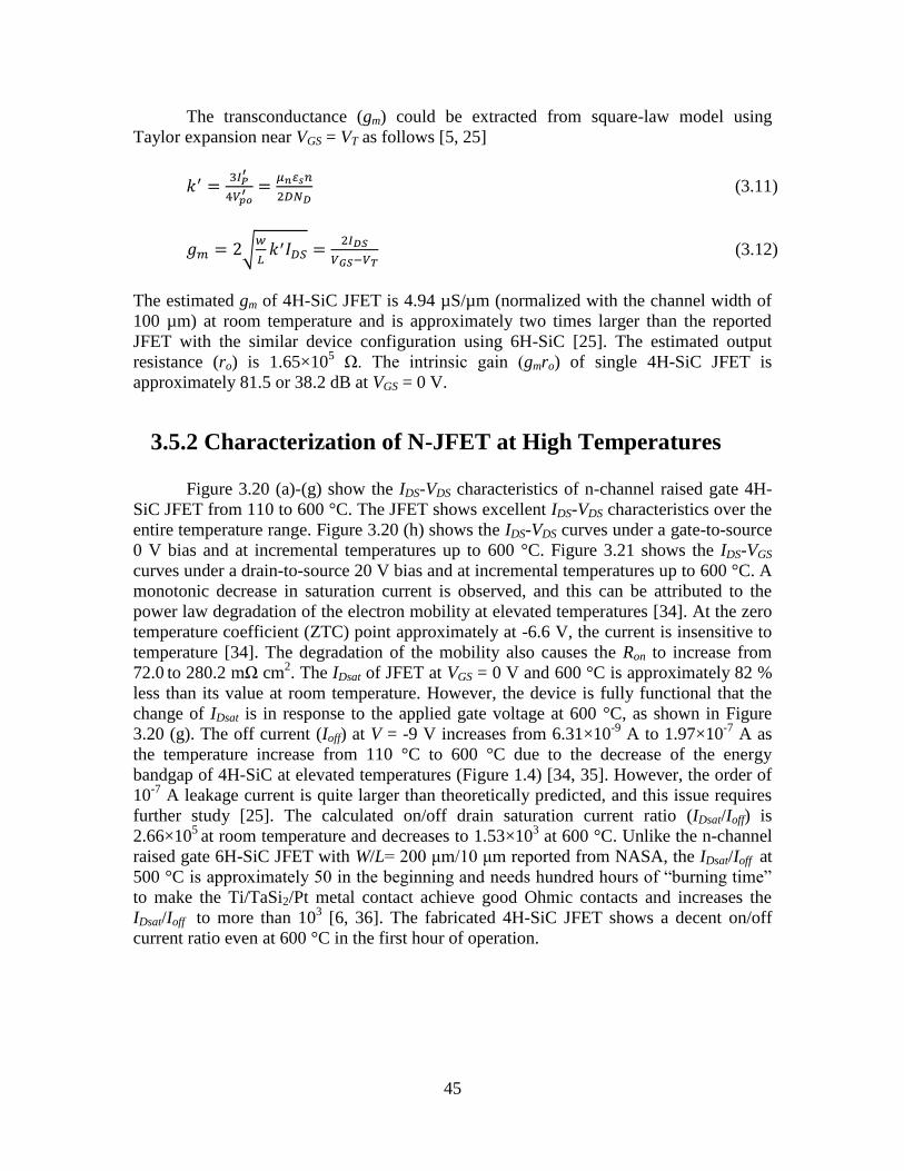
45
The transconductance (gm) could be extracted from square-law model using
Taylor expansion near VGS = VT as follows [5, 25]
𝑛
(3.11)
√
𝐼
(3.12)
The estimated gm of 4H-SiC JFET is 4.94 µS/µm (normalized with the channel width of
100 µm) at room temperature and is approximately two times larger than the reported
JFET with the similar device configuration using 6H-SiC [25]. The estimated output
resistance (ro) is 1.65×10⁵ Ω. The intrinsic gain (gmro) of single 4H-SiC JFET is
approximately 81.5 or 38.2 dB at VGS = 0 V.
3.5.2 Characterization of N-JFET at High Temperatures
Figure 3.20 (a)-(g) show the IDS-VDS characteristics of n-channel raised gate 4H-
SiC JFET from 110 to 600 °C. The JFET shows excellent IDS-VDS characteristics over the
entire temperature range. Figure 3.20 (h) shows the IDS-VDS curves under a gate-to-source
0 V bias and at incremental temperatures up to 600 °C. Figure 3.21 shows the IDS-VGS
curves under a drain-to-source 20 V bias and at incremental temperatures up to 600 °C. A
monotonic decrease in saturation current is observed, and this can be attributed to the
power law degradation of the electron mobility at elevated temperatures [34]. At the zero
temperature coefficient (ZTC) point approximately at -6.6 V, the current is insensitive to
temperature [34]. The degradation of the mobility also causes the Ron to increase from
72.0 to 280.2 mΩ cm
2. The IDsat of JFET at VGS = 0 V and 600 °C is approximately 82 %
less than its value at room temperature. However, the device is fully functional that the
change of IDsat is in response to the applied gate voltage at 600 °C, as shown in Figure
3.20 (g). The off current (Ioff) at V = -9 V increases from 6.31×10⁻⁹
A to 1.97×10⁻⁷
A as
the temperature increase from 110 °C to 600 °C due to the decrease of the energy
bandgap of 4H-SiC at elevated temperatures (Figure 1.4) [34, 35]. However, the order of
10-7
A leakage current is quite larger than theoretically predicted, and this issue requires
further study [25]. The calculated on/off drain saturation current ratio (IDsat/Ioff) is
2.66×10⁵
at room temperature and decreases to 1.53×10³ at 600 °C. Unlike the n-channel
raised gate 6H-SiC JFET with W/L= 200 μm/10 μm reported from NASA, the IDsat/Ioff at
500 °C is approximately 50 in the beginning and needs hundred hours of “burning time”
to make the Ti/TaSi2/Pt metal contact achieve good Ohmic contacts and increases the
IDsat/Ioff to more than 103 [6, 36]. The fabricated 4H-SiC JFET shows a decent on/off
current ratio even at 600 °C in the first hour of operation.
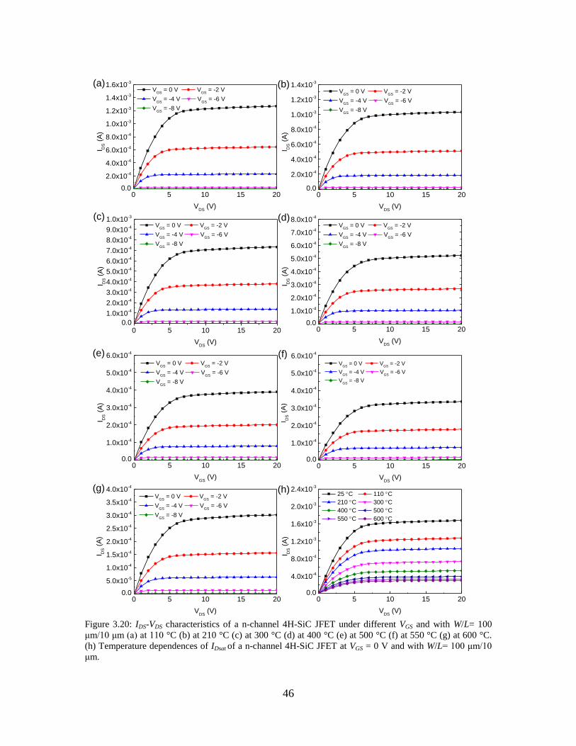
46
Figure 3.20: IDS-VDS characteristics of a n-channel 4H-SiC JFET under different VGS and with W/L= 100
μm/10 μm (a) at 110 °C (b) at 210 °C (c) at 300 °C (d) at 400 °C (e) at 500 °C (f) at 550 °C (g) at 600 °C.
(h) Temperature dependences of IDsat of a n-channel 4H-SiC JFET at VGS = 0 V and with W/L= 100 μm/10
μm.
0 5 10 15 200.0
2.0x10⁻⁴
4.0x10⁻⁴
6.0x10⁻⁴
8.0x10⁻⁴
1.0x10⁻³
1.2x10⁻³
1.4x10⁻³
1.6x10⁻³
I DS (
A)
VDS
(V)
VGS
= 0 V VGS
= -2 V
VGS
= -4 V VGS
= -6 V
VGS
= -8 V
0 5 10 15 200.0
1.0x10⁻⁴
2.0x10⁻⁴
3.0x10⁻⁴
4.0x10⁻⁴
5.0x10⁻⁴
6.0x10⁻⁴
7.0x10⁻⁴
8.0x10⁻⁴
9.0x10⁻⁴
1.0x10⁻³
I DS (
A)
VDS
(V)
VGS
= 0 V VGS
= -2 V
VGS
= -4 V VGS
= -6 V
VGS
= -8 V
0 5 10 15 200.0
1.0x10⁻⁴
2.0x10⁻⁴
3.0x10⁻⁴
4.0x10⁻⁴
5.0x10⁻⁴
6.0x10⁻⁴
7.0x10⁻⁴
8.0x10⁻⁴
I DS (
A)
VDS
(V)
VGS
= 0 V VGS
= -2 V
VGS
= -4 V VGS
= -6 V
VGS
= -8 V
0 5 10 15 200.0
1.0x10⁻⁴
2.0x10⁻⁴
3.0x10⁻⁴
4.0x10⁻⁴
5.0x10⁻⁴
6.0x10⁻⁴
I DS (
A)
VGS
(V)
VGS
= 0 V VGS
= -2 V
VGS
= -4 V VGS
= -6 V
VGS
= -8 V
(a)
0 5 10 15 200.0
2.0x10⁻⁴
4.0x10⁻⁴
6.0x10⁻⁴
8.0x10⁻⁴
1.0x10⁻³
1.2x10⁻³
1.4x10⁻³
I DS (
A)
VDS
(V)
VGS
= 0 V VGS
= -2 V
VGS
= -4 V VGS
= -6 V
VGS
= -8 V
(c)
(e)
(b)
(d)
(f)
(g)
0 5 10 15 200.0
1.0x10⁻⁴
2.0x10⁻⁴
3.0x10⁻⁴
4.0x10⁻⁴
5.0x10⁻⁴
6.0x10⁻⁴
I DS (
A)
VDS
(V)
VGS
= 0 V VGS
= -2 V
VGS
= -4 V VGS
= -6 V
VGS
= -8 V
0 5 10 15 200.0
4.0x10⁻⁴
8.0x10⁻⁴
1.2x10⁻³
1.6x10⁻³
2.0x10⁻³
2.4x10⁻³
I DS (
A)
VDS
(V)
25 C 110 C
210 C 300 C
400 C 500 C
550 C 600 C
0 5 10 15 200.0
5.0x10⁻⁵
1.0x10⁻⁴
1.5x10⁻⁴
2.0x10⁻⁴
2.5x10⁻⁴
3.0x10⁻⁴
3.5x10⁻⁴
4.0x10⁻⁴
I DS (
A)
VDS
(V)
VGS
= 0 V VGS
= -2 V
VGS
= -4 V VGS
= -6 V
VGS
= -8 V
(h)
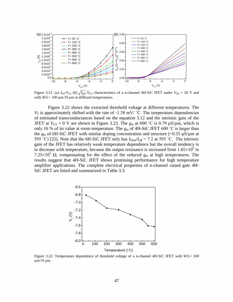
47
Figure 3.21: (a) IDS-VGS (b) √𝐼 -VGS characteristics of a n-channel 4H-SiC JFET under VDS = 20 V and
with W/L= 100 μm/10 μm at different temperatures.
Figure 3.22 shows the extracted threshold voltage at different temperatures. The
VT is approximately shifted with the rate of -1.38 mV/ ˚C. The temperature dependencies
of estimated transconductances based on the equation 3.12 and the intrinsic gain of the
JFET at VGS = 0 V are shown in Figure 3.23. The gm at 600 ˚C is 0.79 µS/µm, which is
only 16 % of its value at room temperature. The gm of 4H-SiC JFET 600 ˚C is larger than
the gm of 6H-SiC JFET with similar doping concentration and structure (~0.55 µS/µm at
595 ˚C) [25]. Note that the 6H-SiC JFET only has IDsat/Ioff = 7.2 at 595 ˚C. The intrinsic
gain of the JFET has relatively weak temperature dependence but the overall tendency is
to decrease with temperature, because the output resistance is increased from 1.65×10⁵ to
7.25×10⁵ Ω, compensating for the effect of the reduced gm at high temperatures. The
results suggest that 4H-SiC JFET shows promising performance for high temperature
amplifier applications. The complete electrical properties of n-channel raised gate 4H-
SiC JFET are listed and summarized in Table 3.3.
Figure 3.22: Temperature dependence of threshold voltage of a n-channel 4H-SiC JFET with W/L= 100
μm/10 μm.
(a) (b)
-10 -8 -6 -4 -2 0
0.00
0.01
0.02
0.03
0.04
0.05
[ID
S/(
1+V
DS)]
0.5
(A0.5)
VGS
(V)
T= 25 C
T= 110 C
T= 210 C
T= 300 C
T= 400 C
T= 500 C
T= 550 C
T= 600 C
-10 -8 -6 -4 -2 0
0.02.0x10
-4
4.0x10⁻⁴
6.0x10⁻⁴
8.0x10⁻⁴
1.0x10⁻³
1.2x10⁻³
1.4x10⁻³
1.6x10⁻³
1.8x10⁻³
2.0x10⁻³
2.2x10⁻³
2.4x10⁻³
I DS (
A)
VGS
(V)
T= 25 C
T= 110 C
T= 200 C
T= 300 C
T= 400 C
T= 500 C
T= 550 C
T= 600 C
0 100 200 300 400 500 600-8.0
-7.8
-7.6
-7.4
-7.2
-7.0
-6.8
-6.6
VT (
V)
Temperature (C)

48
Figure 3.23: Temperature dependence of transconductance and intrinsic gain of of a n-channel 4H-SiC
JFET with W/L= 100 μm/10 μm.
Temperature
(°C) VT (V)
gm
(µS/µm)
Ron (mΩ
cm2)
ro (Ω) λ (mV-1
) gmro IDsat/Ioff
25 -6.81 4.94 59.3 1.65×10⁵ 3.88 81.5 2.66×10
5
110 -6.95 3.65 72.0 2.10×10⁵ 4.03 76.9 9.88×10
4
210 -7.15 2.88 87.3 2.73×10⁵ 3.81 78.6 8.96×10
4
300 -7.19 2.04 123.21 3.20×10⁵ 4.65 65.1 4.24×10
4
400 -7.31 1.43 172.24 4.78×10⁵ 4.33 68.4 2.44×10
4
500 -7.45 1.05 214.00 6.42×10⁵ 4.32 67.3 1.15×10
4
550 -7.60 0.88 249.17 7.32×10⁵ 4.41 64.7 1.56×10
3
600 -7.63 0.79 280.23 7.25×10⁵ 5.02 57.2 1.53×10
3
Table 3.3: Extracted parameters of n-channel raised gate 4H-SiC JFET with W/L= 100 μm/10 μm at various
temperatures. gm, Ron, ro , λ and gmro is based on VGS = 0 V. IDsat/Ioff is the ratio of current at VGS = 0 V and
VGS = -9 V.
3.5.3 Reliability
Compared to Si and III-V semiconductors, 4H-SiC is nearly chemically inert and
has high thermal stability with low atom mobility [37]. However, thermally activated
degradation between metal-SiC interface and other materials, such as the insulator, metal
and packaging, will limit the high temperature durability and consequently hinder the
commercialization of 4H-SiC electronics [5, 6, 24]. Therefore, it is important to study the
reliability of the fabricated 4H-SiC JFET. Two adjacent 4H-SiC n-channel JFET devices
with W/L = 100 μm/10 μm on the same chip were used in this reliability test. Due to the
temperature limitation of the hot-plate, the temperature 540 °C was set up for the
0 100 200 300 400 500 6000
1
2
3
4
5
6
gm
gmr
o
Temperature (C)
gm (
S/
m)
20
30
40
50
60
70
80
gmr o

49
reliability test. The sample was periodically heated to 540 °C on a pre-heated hot-plate in
ambient air. The hot-plate was turned off and the sample is naturally cooled down by air
for at least twenty minutes on the hotplate. The sample was then placed on a high-
temperature probe station for the measurement of I-V characteristics. This method was
repeated hourly for the first twenty hours and then extended to five hour periods. Figure
3.24 shows the IDS-VDS and IDS-VGS characteristics of one JFET at 0, 25th, 50th, 75th, and
90 hours at 540 °C. Figure 3.25 illustrates the measured variation of transconductance for
two n-channel JFETs as a function of 540 °C operating time over 90 hours. The gm is
normalized to the initial value of gm0. The fluctuation of IDS and gm is due to the different
probing forces applied on the metal contact for each measurement. The measured gm
changed less than 10 % and 3 % for the first and second JFETs, respectively, over the 90
hour test at 540 °C. After the 90 hours testing time, the devices no longer exhibited any
transistor characteristics. Figure 3.26 is the optical image of one JFET after 90 hours. The
metal contacts become very rough. The heating and cooling cycle for each test caused the
metal contacts to delaminate due to the thermal stress developed within the three layers of
metal stacks. To avoid this, the device can be bonded to the high temperature ceramic
packaging such as aluminum oxide [5] or aluminum nitride [38, 39]; however, the failure
of the wire bonding must also be considered in the reliability test.
Figure 3.24: (a) IDS-VDS characteristics at VGS = 0 V and (b) IDS-VGS characteristics at VDS = 20 V during 0,
25th, 50th, 75th, and 90 hours of electrical operation at 540 °C for a n-channel 4H-SiC JFET with W/L =
100 μm/10 μm .
(a) (b)
0 5 10 15 200.0
5.0x10⁻⁵
1.0x10⁻⁴
1.5x10⁻⁴
2.0x10⁻⁴
2.5x10⁻⁴
3.0x10⁻⁴
3.5x10⁻⁴
4.0x10⁻⁴
I DS (
A)
VDS
(V)
0 hour
25 hours
50 hours
75 hours
90 hours
-10 -8 -6 -4 -2 00.0
5.0x10⁻⁵
1.0x10⁻⁴
1.5x10⁻⁴
2.0x10⁻⁴
2.5x10⁻⁴
3.0x10⁻⁴
3.5x10⁻⁴
4.0x10⁻⁴
I DS (
A)
VGS
(V)
0 hour
25 hours
50 hours
75 hours
90 hours

50
Figure 3.25: Normalized gm versus test time at 540 °C through 90 hours for a n-channel 4H-SiC JFET with
W/L = 100 μm/10 μm.
Figure 3.26: Optical image of a n-channel 4H-SiC JFET with W/L = 100 μm/10 μm after thermal reliability
test at 540 °C after 90 hours.
3.6 TCAD Simulation of N-Channel Raised Gate JFET
Technology Computer Aided Design (TCAD) device simulator allows the device
engineer to design and optimize the current and other electrical properties for the device.
In this section, Synopsys Sentaurus device simulation was used to model the behavior of
the n-channel raised gate 4H-SiC JFET. Because the Sentaurus process is not fully
functional for 4H-SiC process modeling, we only use the modified example of 4H-SiC
IGBT for doping concentration and distribution of ion implantation which has already
been discussed in Section 3.3. Note that the Silvaco International does offer both process
and device simulation of 4H-SiC [40]. Due to the lack of the access to Silvaco device
0 20 40 60 80 1000.80
0.85
0.90
0.95
1.00
1.05
1.10
Device 1
Device 2
gm/g
m0
Test Time (hours)
51
simulation, Sentaurus structure editor was used to build the two-dimensional device
structure of 4H-SiC as shown in Figure 3.27. The JFET has a gate length of 10 µm and
the source/drain width of 100 µm. The distance between the edge of the gate and the edge
of the source/drain is 5 µm. For comparison, Figure 3.28 shows the I-V curves of the
simulated and measured devices at 25 and 600 °C. In the saturation region, the simulated
device exhibits a similar IDS and ro with the measured one for both at 25 and 600 °C. The
main difference is that the simulated device has smaller VT and leakage current. The VT of
the simulated device at 25 and 600 °C are approximately 4.65 and 5.89 V, respectively,
while the VT of the measured device varies from -6.8 to -7.63 V from 25 to 600 °C. The
leakage current at VGS = -8 V and at 25 and 600 °C are < 10-18
A and 8.16×10⁻¹¹
A,
respectively. The main reasons for these differences could be attribute to:
(1) The quality of material. There are some uncertainties in the material
parameters for the real device, such as doping density of the p-n junction,
defects, etc. The manufacturer specifies a ±5% variation in doping
concentration and thickness of the three epitaxial layers. This contributes to
the different built-in voltage of pn junction. Besides, the defects inside the
channel region may cause the leakage current increases [41, 42]. Figure 3.29
represents an Arrhenius plot of the log of the drain current versus 1/T at VGS =
- 10 V. From the slope fit at different data points, the activation energy is
approximately 0.05 – 0.5 eV. These values are significantly less than the half
the energy bandgap of the 4H-SiC, which means there is an extrinsic leakage
mechanism. This leakage mechanism could either be impurities, defect related,
or a surface oxide conduction process [43]. In this process, the PECVD oxide
was used for the surface passivation and its resistance to the high thermal
heats has not been fully studied, which could contribute the leakage current
path at high temperature [6].
(2) Abrupt interface of nitrogen implanted box and n channel. Sentaurus structure
editor assumes an abrupt interface between implantation box and channel area,
which is not a case in the real fabrication process (Figure 3.5). When the
junction is formed, the current generation at reverse bias can be simplified as
(assuming one side doping is significantly larger than the other side) [39]
𝐼 𝐴 [𝑛
√
+
] (3.13)
Where A is the area of the junction, N is the doping density of the light doping
side, D is the minority diffusion constant, and τ is the effect minority carrier
lifetime. The first term is the minority carrier diffusion current and the second
term is from thermal generation or recombination of carriers that occurs in the
depletion region at a biased diode. The non-abrupt nature of the n+-n junction
and the non-recoverable crystal damage caused by the ion implantation after
thermal annealing must be considered in future TCAD simulation.
(3) Stable Ohmic contact of both p and n junction. The rectifying behavior of
metal contacts at p+ gate in the real device adds to the leakage current path at
high temperature [44].

52
In summary, the built structure for simulation has some deviation from the exact
value of VT and leakage current value, but it can still be used to predict IDsat and the
temperature trend of JFET electrical properties. In the future, calibration of TCAD to the
measured data of JFET will benefit the design optimization study.
Figure 3.27: Raised gate JFET structure generated by the Sentaurus structure editor.
Figure 3.28: Measured and Simulated (a) IDS-VDS characteristics at VGS = 0 V and (b) IDS-VGS characteristics
at VDS = 20 for n-channel 4H-SiC JFETs with W/L = 100 μm/10 μm at 25 and 600 °C.
Figure 3.29: Arrhenius plot of log of drain leakage current versus 1/T at VGS = -10 V of a n-channel 4H-SiC
JFET with W/L = 100 μm/10 μm.
(a) (b)
0 5 10 15 200.0
2.0x10⁻⁴
4.0x10⁻⁴
6.0x10⁻⁴
8.0x10⁻⁴
1.0x10⁻³
1.2x10⁻³
1.4x10⁻³
1.6x10⁻³
1.8x10⁻³
2.0x10⁻³
I DS (
A)
VDS
(V)
Simulation at 25 C
Measurement at 25 C
Simulation at 600 C
Measurement at 600 C
-10 -8 -6 -4 -2 00.0
2.0x10⁻⁴
4.0x10⁻⁴
6.0x10⁻⁴
8.0x10⁻⁴
1.0x10⁻³
1.2x10⁻³
1.4x10⁻³
1.6x10⁻³
1.8x10⁻³
2.0x10⁻³
I DS (
A)
VDS
(V)
Simulation at 25 C
Measurement at 25 C
Simulation at 600 C
Measurement at 600 C
0.0010 0.0015 0.0020 0.0025 0.0030 0.0035-8.4
-8.0
-7.6
-7.2
-6.8
-6.4
log
ID
S
1/T (K-1)

53
3.7 SPICE Parameter Extraction and Device Modeling
To fully realize the SiC JFET integrated circuit technology, simulation of circuit
topology and understanding its high temperature behavior is needed [45-47]. In this
section, the SPICE model of individual JFET is built at temperatures up to 600 °C. A
JFET SPICE DC model level 1 was chosen, and IDS is expressed in SPICE with the
extracted parameters as follows
If VGS-VT < 0,
𝐼 (3.14)
If VDS < VGS-VT,
𝐼 + [ ] (3.15)
If VDS < VGS-VT,
𝐼 + (3.16)
where is the β transconductance coefficient which can be obtained by squaring the slope
of linear function in Figure 3.19 (b). The parameters for the SPICE model are listed in
Table 3.4.
Temperature
(°C) VT (V) β λ (mV
-1)
25 -6.81 3.34×10⁻⁵
3.88
110 -6.95 2.43×10⁻⁵
4.03
210 -7.15 1.83×10⁻⁵
3.81
300 -7.19 1.29×10⁻⁵
4.65
400 -7.31 8.82×10⁻⁶
4.33
500 -7.45 6.30×10⁻⁶
4.32
550 -7.60 5.31×10⁻⁶
4.41
600 -7.63 4.62×10⁻⁶
5.02
Table 3.4: The extracted SPICE parameters of a n-channel 4H-SiC JFET with W/L= 100 μm/10 μm from 25
to 600 °C.
Figure 3.30 compares the measured IDS-VDS with the device simulation with
SPICE. Good agreement between simulations and measurements has been achieved for
all the temperature ranges.
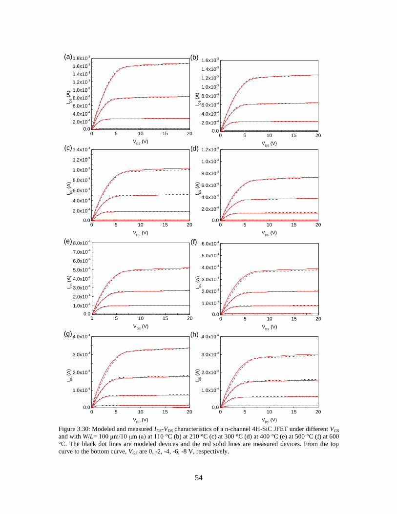
54
Figure 3.30: Modeled and measured IDS-VDS characteristics of a n-channel 4H-SiC JFET under different VGS
and with W/L= 100 μm/10 μm (a) at 110 °C (b) at 210 °C (c) at 300 °C (d) at 400 °C (e) at 500 °C (f) at 600
°C. The black dot lines are modeled devices and the red solid lines are measured devices. From the top
curve to the bottom curve, VGS are 0, -2, -4, -6, -8 V, respectively.
0 5 10 15 200.0
2.0x10⁻⁴
4.0x10⁻⁴
6.0x10⁻⁴
8.0x10⁻⁴
1.0x10⁻³
1.2x10⁻³
1.4x10⁻³
1.6x10⁻³
1.8x10⁻³
I DS (
A)
VDS
(V)
0 5 10 15 200.0
2.0x10⁻⁴
4.0x10⁻⁴
6.0x10⁻⁴
8.0x10⁻⁴
1.0x10⁻³
1.2x10⁻³
1.4x10⁻³
1.6x10⁻³
I DS (
A)
VDS
(V)
0 5 10 15 200.0
2.0x10⁻⁴
4.0x10⁻⁴
6.0x10⁻⁴
8.0x10⁻⁴
1.0x10⁻³
1.2x10⁻³
1.4x10⁻³
I DS (
A)
VDS
(V)
0 5 10 15 200.0
2.0x10⁻⁴
4.0x10⁻⁴
6.0x10⁻⁴
8.0x10⁻⁴
1.0x10⁻³
1.2x10⁻³
I DS (
A)
VDS
(V)
0 5 10 15 200.0
1.0x10⁻⁴
2.0x10⁻⁴
3.0x10⁻⁴
4.0x10⁻⁴
5.0x10⁻⁴
6.0x10⁻⁴
7.0x10⁻⁴
8.0x10⁻⁴
I DS (
A)
VDS
(V)
0 5 10 15 200.0
1.0x10⁻⁴
2.0x10⁻⁴
3.0x10⁻⁴
4.0x10⁻⁴
5.0x10⁻⁴
6.0x10⁻⁴
I DS (
A)
VDS
(V)
0 5 10 15 200.0
1.0x10⁻⁴
2.0x10⁻⁴
3.0x10⁻⁴
4.0x10⁻⁴
I DS (
A)
VDS
(V)
0 5 10 15 200.0
1.0x10⁻⁴
2.0x10⁻⁴
3.0x10⁻⁴
4.0x10⁻⁴
I DS (
A)
VDS
(V)
(a)
(c)
(e)
(b)
(d)
(f)
(g) (h)

55
3.8 Summary
The low voltage, normally on n-channel JFETs with raised gate configuration
using 4H-SiC are fabricated and characterized with operational temperature up to 600 °C.
The threshold voltage at 25 °C is -6.81 with a high transconductance of 4.94 µS/µm and
small on-resistance of 59.3 mΩ cm2. As the temperature increases, the threshold voltage
shifts with the rate of -1.38 mV/ °C. Even at 600 °C, the JFET still exhibits a
transconductance of 0.79 µS/µm and an on/off drain saturation current ratio of 103.
Hence, the SPICE DC fitting model agrees well with the measured data.
3.9 Reference
[1] W. R. Chang, Y. K. Fang, S. F. Ting, Y. S. Tsair, C. N. Chang, C. Y. Lin, and S.
F. Chen, "The hetero-epitaxial SiCN/Si MSM photodetector for high-temperature
deep-UV detecting applications," IEEE Electron Device Letters, vol. 24, pp. 565-
567, Sep 2003.
[2] E. Monroy, F. Omnes, and F. Calle, "Wide-bandgap semiconductor ultraviolet
photodetectors," Semiconductor Science and Technology, vol. 18, pp. R33-R51,
Apr 2003.
[3] A. Vijayakumar, R. M. Todi, and K. B. Sundaram, "Amorphous-SiCBN-B ased
metal-semiconductor-metal photodetector for high-temperature applications,"
IEEE Electron Device Letters, vol. 28, pp. 713-715, Aug 2007.
[4] W.-C. Lien, D.-S. Tsai, D.-H. Lien, D. G. Senesky, J.-H. He, and A. P. Pisano,
"4H–SiC Metal–Semiconductor–Metal Ultraviolet Photodetectors in Operation of
450 °C," 2012.
[5] P. G. Neudeck, S. L. Garverick, D. J. Spry, L. Y. Chen, G. M. Beheim, M. J.
Krasowski, and M. Mehregany, "Extreme temperature 6H-SiC JFET integrated
circuit technology," Physica Status Solidi A, vol. 206, pp. 2329-2345, Oct 2009.
[6] P. G. Neudeck, D. J. Spry, L.-Y. Chen, G. M. Beheim, R. S. Okojie, C. W. Chang,
R. D. Meredith, T. L. Ferrier, L. J. Evans, and M. J. Krasowski, "Stable Electrical
Operation of 6H–SiC JFETs and ICs for Thousands of Hours at 500," IEEE
Electron Device Letters, vol. 29, pp. 456-459, 2008.
[7] D. Brown, E. Downey, M. Ghezzo, J. Kretchmer, V. Krishnamurthy, W.
Hennessy, and G. Michon, "Silicon carbide MOSFET integrated circuit
technology," Physica Status Solidi A, vol. 162, pp. 459-479, 1997.
[8] S.-H. Ryu, K. T. Kornegay, J. A. Cooper Jr, and M. R. Melloch, "Digital CMOS
IC's in 6H-SiC operating on a 5-V power supply," IEEE Transactions on Electron
Devices, vol. 45, pp. 45-53, 1998.
[9] D. Clark, E. P. Ramsay, A. Murphy, D. A. Smith, R. Thompson, R. Young, J. D.
Cormack, C. Zhu, S. Finney, and J. Fletcher, "High temperature silicon carbide
CMOS integrated circuits," in Materials Science Forum,2011, pp. 726-729.

56
[10] C.-W. Soong, A. C. Patil, S. L. Garverick, F. XIAOAN, and M. Mehregany, "550
C integrated logic circuits using 6H-SiC JFETs," IEEE Electron Device Letters,
vol. 33, pp. 1369-1371, 2012.
[11] S. L. Garverick, C.-W. Soong, and M. Mehregany, "SiC JFET integrated circuits
for sensing and control at temperatures up to 600° C," in IEEE Energytech 2012,
2012, pp. 1-6.
[12] L. Lanni, R. Ghandi, B. G. Malm, C. Zetterling, and M. Ostling, "Design and
characterization of high-temperature ECL-based bipolar integrated circuits in 4H-
SiC," IEEE Transactions on Electron Devices, vol. 59, pp. 1076-1083, 2012.
[13] M. Domeij, M. Ö stling, C. M. Zetterling, R. Ghandi, B. Buono, and B. G. Malm,
"Current Gain Degradation in 4H-SiC Power BJTs," in Materials Science Forum,
2011, pp. 702-705.
[14] B. Ozpineci and L. Tolbert, "Smaller, faster, tougher," IEEE Spectrum, vol. 48, pp.
45-66, 2011.
[15] C.-M. Zetterling, Process technology for silicon carbide devices: IET, 2002.
[16] R. F. Pierret, Semiconductor device fundamentals: Pearson Education India, 1996.
[17] S. M. Sze and K. K. NG, Physics of semiconductor devices: Wiley, 2007.
[18] P. G. Neudeck, G. M. Beheim, and C. S. Salupo, "600 C Logic Gates Using
Silicon Carbide JFET's," in 2000 Government Microcircuit Applications
Conference, March, 2000, pp. 20-23.
[19] M. Laube, F. Schmid, G. Pensl, G. Wagner, M. Linnarsson, and M. Maier,
"Electrical activation of high concentrations of N+ and P
+ ions implanted into 4H–
SiC," Journal of Applied Physics, vol. 92, pp. 549-554, 2002.
[20] M. V. Rao, J. B. Tucker, M. Ridgway, O. Holland, N. Papanicolaou, and J.
Mittereder, "Ion-implantation in bulk semi-insulating 4H–SiC," Journal of
Applied Physics, vol. 86, pp. 752-758, 1999.
[21] S.-K. Lee, C.-M. Zetterling, M. Ö stling, J.-P. Palmquist, and U. Jansson, "Low
resistivity ohmic contacts on 4H-silicon carbide for high power and high
temperature device applications," Microelectronic Engineering, vol. 60, pp. 261-
268, 2002.
[22] S. Lee, C.-M. Zetterling, and M. Ostling, "Titanium Tungsten (TiW) for Ohmic
contacts to n-and p-type 4H-SiC," in Materials Research Society Symposium
Proceedings, 2001, pp. H7. 2-H7. 2.
[23] C. Chang, Y. Fang, and S. Sze, "Specific contact resistance of metal-
semiconductor barriers," Solid-State Electronics, vol. 14, pp. 541-550, 1971.
[24] A. B. Horsfall, N. G. Wright, H. K. Chan, J. P. Goss, and R. C. Stevens,
"Reliability Evaluation of 4H-SiC JFETs Using IV Characteristics and Low
Frequency Noise," in Materials Science Forum, 2013, pp. 934-937.
[25] A. C. Patil, "Silicon Carbide JFET Integrated Circuit Technology For High-
Temoerature Sensors," Electrical Engineering and Computer Science, Case
Western Reserve University, 2009.
[26] E. Luckowski, J. Delucca, J. Williams, S. Mohney, M. Bozack, T. Isaacs-Smith,
and J. Crofton, "Improved ohmic contact to n-type 4H and 6H-SiC using
nichrome," Journal of Electronic Materials, vol. 27, pp. 330-334, 1998.
57
[27] S.-K. Lee, C.-M. Zetterling, M. Ö stling, J.-P. Palmquist, H. Högberg, and U.
Jansson, "Low resistivity ohmic titanium carbide contacts to n-and p-type 4H-
silicon carbide," Solid-State Electronics, vol. 44, pp. 1179-1186, 2000.
[28] L. Fursin, J. Zhao, and M. Weiner, "Nickel ohmic contacts to p and n-type 4H-
SiC," Electronics Letters, vol. 37, pp. 1092-1093, 2001.
[29] R. S. Okojie, L. J. Evans, D. Lukco, and J. P. Morris, "A Novel Tungsten–Nickel
Alloy Ohmic Contact to SiC at 900," IEEE Electron Device Letters, vol. 31, pp.
791-793, 2010.
[30] S. Tsukimoto, T. Sakai, and M. Murakami, "Electrical properties and
microstructure of ternary Ge/Ti/Al ohmic contacts to p-type 4H–SiC," Journal of
Applied Physics, vol. 96, pp. 4976-4981, 2004.
[31] R. Kakanakov, L. Kassamakova, I. Kassamakov, K. Zekentes, and N. Kuznetsov,
"Improved Al/Si ohmic contacts to p-type 4H-SiC," Materials Science and
Engineering: B, vol. 80, pp. 374-377, 2001.
[32] F. Laariedh, M. Lazar, P. Cremillieu, J. Penuelas, J. Leclercq, and D. Planson,
"The role of nickel and titanium in the formation of ohmic contacts on p-type 4H–
SiC," Semiconductor Science and Technology, vol. 28, p. 045007, 2013.
[33] D. Planson, C. Raynaud, M. Lazar, D. Tournier, M. Soueidan, and D. M. Nguyen,
"Process Optimization for High Temperature SiC Lateral Devices," in Materials
Science Forum, 2009, pp. 585-588.
[34] V. Lauer, E. Niemann, S. Sheppard, and W. Wondrak, "High temperature
performance of implanted-gate n-channel JFETs in 6H-SiC," in Materials Science
Forum, 1997, pp. 1077-1080.
[35] T. Ayalew, "SiC Semiconductor Devices Technology, Modeling, and Simulation
", Technical University of Vienna, 2004.
[36] R. S. Okojie, D. Lukco, Y. L. Chen, and D. J. Spry, "Reliability assessment of
Ti/TaSi 2/Pt ohmic contacts on SiC after 1000 h at 600 C," Journal of Applied
Physics, vol. 91, pp. 6553-6559, 2002.
[37] A. A. Stephen E. Saddow, Advances in Silicon Carbide Processing and
Applications, 2004.
[38] A. Maralani and M. S. Mazzola, "The design of an operational amplifier using
silicon carbide JFETs," IEEE Transactions on Circuits and Systems I: Regular
Papers, vol. 59, pp. 255-265, 2012.
[39] P. G. Neudeck, R. S. Okojie, and L.-Y. Chen, "High-temperature electronics-a
role for wide bandgap semiconductors?," Proceedings of the IEEE, vol. 90, pp.
1065-1076, 2002.
[40] V. Cell and T. Videos, "State of the Art 3D SiC Process and Device Simulation."
[41] Q. Wahab, A. Ellison, A. Henry, E. Janzén, C. Hallin, J. Di Persio, and R.
Martinez, "Influence of epitaxial growth and substrate-induced defects on the
breakdown of 4H–SiC Schottky diodes," Applied Physics Letters, vol. 76, pp.
2725-2727, 2000.
[42] T. Kimoto, N. Miyamoto, and H. Matsunami, "Performance limiting surface
defects in SiC epitaxial pn junction diodes," , IEEE Transactions on Electron
Devices vol. 46, pp. 471-477, 1999.

58
[43] F. McLean, C. Tipton, J. McGarrity, and C. Scozzie, "Modeling the electrical
characteristics of n‐channel 6H–SiC junction‐field‐effect transistors as a function
of temperature," Journal of Applied Physics, vol. 79, pp. 545-552, 1996.
[44] H. Daimon, M. Yamanaka, M. Shinohara, E. Sakuma, S. Misawa, K. Endo, and S.
Yoshida, "Operation of Schottky‐barrier field‐effect transistors of 3C‐SiC up to
400° C," Applied Physics Letters, vol. 51, pp. 2106-2108, 1987.
[45] S. Zappe, E. Obermeier, S. Sheppard, U. Schmid, V. Lauer, and W. Wondrak,
"Advanced SPICE-modelling of 6H-SiC-JFETs including substrate effects," in
1998 Fourth International High Temperature Electronics Conference, 1998, pp.
261-264.
[46] Y. Wang, C. J. Cass, T. P. Chow, F. Wang, and D. Boroyevich, "SPICE model of
SiC JFETs for circuit simulations," in Computers in Power Electronics, 2006.
COMPEL'06. IEEE Workshops on, 2006, pp. 212-215.
[47] R. Mousa, D. Planson, H. Morel, B. Allard, and C. Raynaud, "Modeling and high
temperature characterization of SiC-JFET," in IEEE Power Electronics
Specialists Conference, 2008, pp. 3111-3117.

59
Chapter 4
Silicon Carbide Complementary Buried
Gate Junction Field-Effect Transistors
4.1 Introduction
CMOS is widely used for constructing integrated circuits, both digital logic and
analog circuits. The advantages of using complementary devices are high noise
immunity, larger bandwidth, and low power consumption [1, 2]. Certain applications,
such as in-situ monitoring of fuel combustion, subsurface reservoirs (deep well drilling),
and Venus and Jupiter surface exploration, require the electronics and their circuitry to
work in the temperature range of 300-600 °C [3]. However, the operating temperature of
Si CMOS devices, both bulk and silicon-on-insulator, is limited to 400 °C due to the
more intrinsic carriers present than dopants carriers at this temperature [3-5]. Silicon
carbide has become the candidate for these harsh environment electronics and circuitry
because of its wide bandgap (3.2 eV for 4H-SiC), excellent chemical and thermal
stability, and high breakdown electric field strength (5 MV/cm) [6]. However, much
effort has been dedicated to the development of SiC n-channel transistors, and several
reports show promising electrical properties of SiC n-channel devices, such as MOSFET
[7], JFET [8] and BJT [9]. On the other hand, very few papers have reported SiC p-
channel transistors. The reasons is that the hole mobility of SiC is more than eight times
smaller than electron mobility [10] and the thermal activation energy of p-type dopants is
higher than n-type dopants [11]. While SiC MOSFET suffers from the low inversion
mobility and gate oxide reliability issues limiting the operating temperature up to 400 °C
[12-14], majority-carrier JFET seems to be a promising candidate for complementary
transistors.
In this chapter, we first propose the fabrication process of 4H-SiC complementary
JFETs (c-JFETs). Despite the lack of success with an of the n-channel buried gate JFET
(n-JFET), we have developed the first prototype of the low voltage, p-channel buried gate
JFET (p-JFET) using 4H-SiC and characterize the electrical properties from room
temperature up to 600 °C in air.
4.2 Design of Complementary Buried Gate JFET

60
To design and optimize the performance of the complementary device, Sentaurus
TCAD structure editor was used to build the two-dimensional device structure of 4H-SiC
as shown in Figure 4.1. The JFET has a gate length of 10 µm and the source/drain width
of 100 µm. The distance between the edge of the gate and the edge of the source/drain is
5 µm.
Figure 4.1: Buried gate JFET structure generated by the Sentaurus structure editor.
A previous study shows that the VT is most sensitive to the depth of the channel
and gate, and doping concentration of the channel [15]. To reduce the number steps in the
lithography process, the depth of the p+ gate of n-JFET and the depth of the p
+
source/drain p-JFET are fixed with the same value of 50 nm, as in the n+ case. Therefore,
the simulation focuses mainly on the effects of the channel depth and doping
concentration for both p- and n-JFETs. Figures 4.2 and 4.3 show examples of effects of
the channel depth and doping concentration to both n- and p-JFETs with L = 8 μm at
room temperature. In order to achieve the low power, complementary JFET circuitry, the
threshold voltage of p- (VTp) and n-JFET (VTn) and the saturation current of p- (IDsat,p) and
n-JFET (IDsat,n) should match with one another. The goal of the optimization of the
parameters is as follows:
(1) |VTp| = |VTn| = ~ 5 V
(2) |IDsat,p| = |IDsat,n| = ~ 10-5
-10-6
A
Figure 4.2: Simulated IDS-VGS of n-channel JFETs with L = 8 µm and (a) different channel doping with
fixed channel depth of 250 nm (b) different channel depth with fixed channel doping of 2.5×10¹⁷
cm-3
at 25
°C.
-20 -15 -10 -5 010
-1510
-1410
-1310
-1210
-1110
-1010
-910
-810
-710
-610
-510
-410
-310
-210
-1
I DS (
A)
VGS
(V)
250 nm 300 nm
350 nm 400 nm
450 nm
-8 -7 -6 -5 -4 -3 -2 -1 010
-1510
-1410
-1310
-1210
-1110
-1010
-910
-810
-710
-610
-510
-410
-310
-210
-1
I DS (
A)
VGS
(V)
ND = 1.510
17 cm
-3
ND = 2.510
17 cm
-3
ND = 310
17 cm
-3
(a) (b)

61
Figure 4.3: Simulated IDS-VGS of p-channel JFETs with L = 8 µm and (a) different channel doping with
fixed channel depth of 400 nm (b) different channel depth with fixed channel doping of 1.5×10¹⁷
cm-3
at 25
°C.
Based on the simulation results, it is not easy to achieve the same intensity of
saturation current with the same intensity of threshold voltage for both p- and n-JFET due
to the smaller hole mobility compared with the electron mobility of 4H-SiC. The strategy
of the optimization is to have similar voltage for both devices and a larger width of
source/drain area or multi-finger gates of p-JFET. Figure 4.4 and Table 4.1 show and
summarize the optimized IDS-VGS curves and parameters of complementary JFETs for
gate length of 8 µm.
Figure 4.4: Simulated IDS-VGS of a (a) n-channel (b) p-channel JFET with L = 8 µm.
0 5 10 15 2010
-1510
-1410
-1310
-1210
-1110
-1010
-910
-810
-710
-610
-510
-410
-310
-210
-1
I DS (
A)
VGS
(V)
350 nm 400 nm
500 nm 600 nm
0 1 2 3 4 5 6 7 810
-1510
-1410
-1310
-1210
-1110
-1010
-910
-810
-710
-610
-510
-410
-310
-210
-110
0
I DS (
A)
VGS
(V)
NA = 1.210
17 cm
-3
NA = 1.510
17 cm
-3
NA = 210
17 cm
-3
(a) (b)
-10 -8 -6 -4 -2 0
0.0
5.0x10⁻⁷
1.0x10⁻⁶
1.5x10⁻⁶
2.0x10⁻⁶
2.5x10⁻⁶
3.0x10⁻⁶
I DS (
A)
VGS
(V)
T = 300 K
T = 600 K
T = 900 K
(a) (b)
0 2 4 6 8 10
0.05.0x10
-8
1.0x10⁻⁷
1.5x10⁻⁷
2.0x10⁻⁷
2.5x10⁻⁷
3.0x10⁻⁷
3.5x10⁻⁷
4.0x10⁻⁷
4.5x10⁻⁷
5.0x10⁻⁷
5.5x10⁻⁷
|ID
S| (A
)
VGS
(V)
T = 300 K
T = 600 K
T = 900 K

62
Device type Temperature (°C) VT (V) gm (µS/µm) ro (Ω)
n 25 -1.3 3.15 4.08×10⁸
n 600 -2.3 0.957 8.81×10⁸
p 25 2 0.111 8.29×10⁸
p 600 3.5 0.257 3.30×10⁸
Table 4.1: Optimized parameters of complementary JFETs with L = 10 µm. gm, ro, and gmro is based on VGS
= 0 V.
Note that the saturation current of p-JFET increases from 25 °C to 327 °C and
then decreases from 327 °C to 627 °C. Unlike the case of the 4H-SiC n-channel JFET
where IDS and gm decrease as temperature increases, these trends of 4H-SiC p-channel
JFET acting in an opposite direction can be attributed to the effect of carrier mobility and
degree of ionization with elevated temperature. The saturation current will increase by
increasing the carrier mobility and ionized carrier concentration as shown in the
conventional 3/2 power model [16]. The electron and hole mobility, µn and µp, at low
electric field could be calculated using Caughey-Thomas equation given by [17]
𝑛 𝑝 𝑛 𝑝 𝑛 +
(4.1)
𝑛 𝑝 𝑛 𝑛 𝑝
𝑛
(4.2)
𝑛 𝑝 𝑎 𝑛 𝑝
𝑎
(4.3)
where ND and NA are the doping concentration of the dopants and acceptors, which are
2.5×10¹⁷
cm-3
and 2.5×10¹⁷
cm-3
, respectively. The µn,pmax
is the mobility of
unintentionally doped 4H-SiC, where the lattice scattering is the main scattering
mechanism. The µn,pmin
is the mobility of heavily doped 4H-SiC, where the dominant
mechanism is impurity scattering. The values of µn,pmax
and µn,pmin
at 300 K are
µn,p(300K)max
and µn,p(300K)min
, respectively. Nn,pref
is the doping concentration at which the
mobility is half of the sum of µn,pmax
and µn,pmin
. αn,pµ denotes how fast the mobility
changes from µn,pmin
to µn,pmax
, βn,pµ is the constant temperature coefficient, and γn,p
µ
describes how mobility of undoped 4H-SiC changes due to lattice scattering. All the
parameters except ND and NA are the fitting parameters and are listed in the Table 4.2
[17].

63
Doping type µn,p(300K)
min
(cm2/Vs)
µn,p(300K)max
(cm2/Vs)
Nn,pref
(cm-3) αn,p
µ βn,p
µ γn,p
µ
n 40 950 1.94×10¹⁷
0.61 -0.5 -2.40
P 15.9 125 1.76×10¹⁹
0.34 -0.5 -2.15
Table 4.2: Fitting parameters for low field mobility of 4H-SiC.
Figure 4.5 (a) shows the temperature dependence of the carrier mobility. The
electron mobility decreases from ~526 cm2/Vs at 300 K to ~294 cm
2/Vs at 900 K for n-
type 4H-SiC, and the hole mobility decreases from ~102 cm2/Vs at 300 K to ~11 cm
2/Vs
at 900 K for p-type 4H-SiC. Both electron and hole mobility decrease as temperature
increases. Therefore, a certain portion of saturation current is reduced due to the
decreases of the carrier mobility. Note that the hole mobility is smaller than electron
mobility, which leads to lower transconductance is p-channel JFET. On the other hand,
most of the common dopants in 4H-SiC, which are nitrogen and phosphorus for n-type,
and boron and aluminum for p-type, have activation energies larger than the thermal
energy at room temperature [18]. This leads the incomplete ionization of these dopants
and strong temperature and frequency dependence of junction differential admittance
[19]. The degree of ionization could be calculated as follows [17]
𝐼𝑛
√
+
√
(4.4)
𝐼𝑝
√
(4.5)
where In and Ip are degree of ionization for nitrogen and aluminum, respectively, ND+ and
NA+ are concentration of ionized donors and acceptors, respectively, gD and gA are
degeneracy factor with value of 2 and 4, respectively, NC and NV are effective density of
states of the conduction band and valence band, respectively, ΔEDh, ΔEDk and ΔEA are
ionization energy of nitrogen on hexagonal site, nitrogen on cubic site and aluminum,
respectively, kB is Boltzmann and T is temperature. The estimated degrees of ionization
of electron and hole are shown in Figure 4.5 (b). The electrons in 4H-SiC already have 82
% of ionization at 25 °C, and they reach nearly 100% ionization at 600 °C. For n-channel
JFET, such a small increase of degree of ionization cannot counterbalance the decrease of
saturation current caused by the electron mobility degradation. However, the holes in 4H-
SiC only have 11% ionization at 25 °C, but they reach 93% ionization at 600 °C, because
the acceptor level of aluminum is relatively deeper (ΔEA = 200 meV) than nitrogen (ΔEDh
= 50 meV and ΔEDk = 92 meV) in 4H-SiC. The significant amount activation of
aluminum acceptors in 4H-SiC accounts for increase of the saturation current at higher
temperature.

64
Figure 4.5: Temperature dependence of (a) carrier mobility and (b) degree of ionization.
4.3 Fabrication Process
Figure 4.6 is a cross-sectional schematic of the lateral 4H-SiC complementary
JFETs used in this work. The transistor consists of n-type 4H-SiC wafer (from SiCrystal
AG) with four epitaxial layers (from Ascatron AB). A 5 µm p- epitaxial layer with doping
concentration of 2×10¹⁵
cm-3
, followed by 250 nm n epitaxial layer with doping
concentration of 1×10¹⁹
cm-3
, a 400 nm p+ epitaxial layer with doping concentration of
1.5×10¹⁷
cm-3
, and a 250 nm n+ epitaxial layer with doping concentration of 2.5×10
17 cm
-
3 were grown on the substrate. Figure 4.7 presents the entire fabrication process flow
including eight lithography masks. First, the device area of n-JFET is time etched using
TCP etcher with 90 sccm Cl2 and 10 sccm BCl3 under RF bias of 150 W. Secondly, the
device area of p-JFET is also time etched using TCP etcher with 90 sccm Cl2 and 10
sccm BCl3 under RF bias of 150 W. 1 μm PECVD SiO2 was patterned to define the
source/drain area of n-JFET and gate area of p-JFET with ion implantation to form n+
box profile at 600 °C. Unlike using nitrogen for the ion implanted n+ region of n-channel
raised gate JFET, as discussed in Chapter 3, phosphorous was used for ion implantation.
The nitrogen forms a donor state when substituting for carbon in the SiC lattice while
phosphorous form a donor state on substituting Si sites [20]. The phosphorous implanted
n+ region can reach above 10
20 cm
-3 while nitrogen implanted one will saturate at 2 to
3×10¹⁹
cm-3
due to the limitation of solubility of nitrogen and formation of nitrogen-
related precipitates [21, 22]. The phosphorous implantation in this work used 1.5×10¹⁵
does at 5 keV. The phosphorous doping concentration and distribution determined from
TCAD simulation are presented in Figure 4.8. The oxide masks were then removed by
buffer oxide etching solution (hydrofluoric acid). 1 μm PECVD SiO2 was patterned to
define the gate area of n-JFET and source/drain area of p-JFET with aluminum
implantation at 600 °C. The implantation of a box profile was formed using 1×10¹⁵
and
1×10¹⁵
doses at 5 and 7 keV energies, respectively. The phosphorous doping
concentration and distribution determined TCAD simulation are presented in Figure 4.9.
After ion implantation, oxide layers were removed by buffer oxide etching solution. The
implanted dopants were electrically activated by annealing samples capped with 2 µm
PECVD SiO2 at 1550 °C under Argon atmosphere for 15 minutes [23]. Figure 4.10 is the
(a) (b)
300 400 500 600 700 800 9000
100
200
300
400
500
600
Mob
ility
(cm
2/V
s)
Temperature (K)
Electron
Hole
300 400 500 600 700 800 900
0.2
0.4
0.6
0.8
1.0
Degre
e o
f io
niz
ation
Temperature (K)
Electron
Hole

65
SEM image of the 4H-SiC after annealing, and there are some etching pits present on the
surface. Better capping technology such as graphite or extra SiC resource is required for
the future fabrication [21, 24]. A mesa etch was then used to define the device area and
expose the base region of p-JFET using TCP etcher. The JFET surface was then
passivated with PECVD SiO2 and the 25 nm Ni, 45 nm Ti, 95 nm Al and 50 nm TiW
(10% Ti, 90% W) contact was deposited and patterned via lift-off to form the contact
electrodes. The metal contacts were annealed via rapid thermal annealing (RTA) at 800
°C for 2 minute under Ar ambient. 200 nm TiW (10% Ti, 90% W) was used for the 1st
level of metal interconnects. Finally, the 20 nm Cr and 180 nm Pt was used for 2nd
level
of metal interconnect.
Figure 4.6: Schematic of 4H-SiC complementary JFETs.
4H-SiC n type Substrate
p- 4H-SiC (NA= 1E15 cm-3)
n+ 4H-SiC (ND= 1E19 cm-3)
p 4H-SiC (NA= 1.5E17 cm-3)
n-epi (ND= 2.5E17 cm-3) 250 nm
400 nm
250 nm
5 µm
50 nm
PJFET
NJFET
SiO2 mask
4H-SiC p+ region
Contact electrode
4H-SiC n+ region

66
Figure 4.7: Completed fabrication process flow of 4H-SiC c-JFETs.
4H-SiC n type Substrate
p- 4H-SiC (NA= 1E15 cm-3)
n+ 4H-SiC (ND= 1E19 cm-3)
p 4H-SiC (NA= 1.5E17 cm-3)
1. Procure SiC substrate with four epi-layers
n 4H-SiC (ND= 2.5E17 cm-3)
3. Micromachine SiC p epi-layer with timed etch
(Mask 2)
2. Micromachine SiC n epi-layer with timed etch (Mask
1)
5. . Deposit conformal SiO2 mask (Spacers), open vias
(Mask 4), ion implant p+ region, and annealing
4. . Deposit conformal SiO2 mask (Spacers), open
vias (Mask 3), and ion implant n+ region
6. Passivate structure with conformal SiO2 and open
metal contact vias (Mask 5)
7. Series steps of metal depositions: Deposit metal
contacts, passivate structure with conformal SiO2,
open metal contact vias (Mask 6), deposit 1st metal
contacts, passivate structure with conformal SiO2 and
open interconnect vias (Mask 7), and deposit 2nd
metal (Mask 8).
4H-SiC substrate
4H-SiC p- epi-layer
4H-SiC n+ epi-layer
4H-SiC p epi-layer
SiO2 mask
4H-SiC p+ region
Contact electrode
4H-SiC n epi-layer
4H-SiC n+ region

67
Figure 4.8: Simulated phosphorous doping profile in the p-channel area with NA = 1.5×10
17 cm
-3.
Figure 4.9: Simulated aluminum doping profile in the n-channel area with ND = 2.5×10
17 cm
-3.
Devices were characterized on a hot chuck of high temperature probe station
(Signatone Inc.). This high temperature probe station consists of ceramic hot chunk,
thermal heater and water cooler and the chunk temperature goes up to 600 °C with low
thermal noise of 10-9
-10-8
A at 600 °C. An Agilent B2912A precision
source/measurement unit and with tungsten probe tips was used to measure the I-V
characteristics of the devices.

68
Figure 4.10: SEM image of etching pits after thermal annealing at 1550 °C for 15 minute.
4.4 Metallization of Complementary Buried Gate JFET
Figure 4.11 shows the I-V measurement of Ni/Ti/Al/TiW metal stacks and n-type
4H-SiC for TLM structure. The contact is originally Ohmic with large resistance before
RTA and the resistance decreases after the RTA. This is possible because the doping
concentration of phosphorous in 4H-SiC achieves more than 1020
cm-3
and a high degree
of ionization even at room temperature, as shown in Figure 4.8. The temperature
dependences of measured ρc are shown in Figure 4.12, and the value of ρc is on the order
of 10-5
Ω cm2 up to 550 °C, indicating a stable metal contact is formed after RTA. The
monotonic increase of the specific contact resistance with temperature is due to the
increases of the tunneling effective mass of carriers at a high doping range of 1020
-1021
cm-3
[25]. Typically, a smaller tunneling effective mass has a smaller ρc value. Possible
instability or oxidation might be responsible for the sudden increase of ρc to 3.383×10⁻⁴
Ω
cm2 at 600 °C. The fitted ρc and Rsh are listed in Table 4.3.

69
Figure 4.11: Measure I-V curves of metal and n-type 4H-SiC before and after RTA annealing for TLM
structure with d = 5 µm.
Figure 4.12: Temperature dependences of specific contact resistance of Ni/Ti/Al/TiW metal stacks to n
+
4H-SiC.
-10 -5 0 5 10-0.15
-0.10
-0.05
0.00
0.05
0.10
0.15
Curr
en
t (A
)
Voltage (V)
With RTA
Without RTA
0 100 200 300 400 500 6000.0
1.0x10⁻⁴
2.0x10⁻⁴
3.0x10⁻⁴
4.0x10⁻⁴
c (
cm
2)
Temperature (C)

70
Temperature
(°C) Rsh (kΩ/□) ρc (Ω cm
2)
25 1.324 3.20×10⁻⁵
110 1.381 3.54×10⁻⁵
210 1.480 3.86×10⁻⁵
300 1.566 4.31×10⁻⁵
400 1.686 5.06×10⁻⁵
500 1.678 6.68×10⁻⁵
550 1.745 8.37×10⁻⁵
600 1.586 3.383×10⁻⁴
Table 4.3: Sheet resistance and specific contact resistance of Ni/Ti/Al/TiW metal stacks and n-type 4H-SiC
at different temperatures.
The I-V measurement of Ni/Ti/Al/TiW metal stacks and n-type 4H-SiC for TLM
structure is shown in Figure 4.13. The contact is Schottky contact before RTA and it
becomes Ohmic after the RTA. The temperature dependencies of measured ρc are shown
in Figure 4.14, and the value of ρc is on the order of 10-3
Ω cm2 which is higher than the
n-type case. Although the p-type doping concentration should reach more than 1020
cm-3
after aluminum ion implantation based on the TCAD simulation (Figure 4.9), specific
contact resistance decreased with temperature up to 550 °C due to the higher degree of
ionization and the current density at elevated temperature. Again, the sudden change of ρc
value at 600 C implies a possible oxidation mechanism or the metal instability. Table 4.4
summarizes the value of Rsh and ρc. The Rsh is at least one order of magnitude higher than
for the n-type case due to the low hole mobility and less degree of ionization.
Figure 4.13: Measure I-V curves of metal and p-type 4H-SiC before and after RTA annealing for TLM
structure with d = 20 µm.
-10 -5 0 5 10-0.0005
0.0000
0.0005
Cu
rre
nt
(A)
Voltage (V)
With RTA
Without RTA

71
Figure 4.14: Temperature dependences of specific contact resistance of Ni/Ti/Al/TiW metal stacks to p
+
4H-SiC.
Temperature (°C) Rsh (kΩ/□) ρc (Ω cm2)
25 170 5.45×10⁻³
110 99.2 3.27×10⁻³
210 62.7 2.28×10⁻³
300 48.3 1.50×10⁻³
400 38.9 1.56×10⁻³
500 37.5 8.14×10⁻⁴
550 35.1 9.92×10⁻⁴
600 33.3 1.07×10⁻³
Table 4.4: Sheet resistance and specific contact resistance of Ni/Ti/Al/TiW metal stacks and p-type 4H-SiC
at different temperatures.
4.5 Electrical Properties of N-Channel Buried Gate
JFET
Figure 4.15 shows the optical image of as-fabricated n-channel buried gate 4H-
SiC JFET with L = 10 μm and W = 100 μm. Figure 4.16 shows the IDS-VDS characteristics
of a 100 μm /10 μm JFET at room temperature. The device exhibits resistor-like behavior
with a very small output resistance at VGS = 0 V. Furthermore, the device cannot
completely turn off by applying a gate bias from 0 V to -10 V which means the JFET is
not fully functional. By inspecting the I-V curve between p+ gate and n channel as shown
in Figure 4.17, the built-in voltage is approximately 2.9 V which is similar to the
0 100 200 300 400 500 6000.0
1.0x10⁻³
2.0x10⁻³
3.0x10⁻³
4.0x10⁻³
5.0x10⁻³
6.0x10⁻³
c (
cm
2)
Temperature (C)

72
theoretical value of 3.11 V. However, as the intensity of drain current did not change with
the gate bias, the possible failure point might be the unsuccessful fabrication of the p+
gate. More characterization techniques such as cross-sectional TEM and secondary ion
mass spectrometry (SIMS) analysis are necessary to verify the doping distribution and
concentration of p+ gate.
Figure 4.15: Optical image of a n-channel buried gate 4H-SiC JFET with L = 10 μm and W = 100 μm.
Figure 4.16: IDS-VDS characteristics of a n-channel buried gate 4H-SiC JFET under different VGS and with
W/L= 100 μm/10 μm at 25 °C.
0 5 10 150.0
2.0x10⁻⁴
4.0x10⁻⁴
6.0x10⁻⁴
VGS
= 0 V
I DS (
A)
VDS
(V)
VGS
= -10 V

73
Figure 4.17: I-V characteristics of pn junction in the n-channel buried gate 4H-SiC JFET structure.
4.6 Electrical Properties of P-Channel Buried Gate
JFET
4.6.1 Characterization of P-Channel Buried Gate JFET at
Room Temperature
Figure 4.18 shows the optical images of as-fabricated p-channel 4H-SiC JFET
with L equal to 10 μm and W equals to 100 μm. The p-channel thickness is approximately
370 nm which is slightly different than the target thickness of 400 nm due to the
imprecise control of etching time. Figure 4.19 shows the drain current (|IDS|) versus VDS
characteristics of a 100 μm /10 μm JFET at room temperature. The characteristic curves
clearly show the linear and saturation regions. The device is a depletion mode JFET
which is fully-on at VGS = 0 V and is cut-off at VGS = 5 V. Figure 4.20 (a) is the |IDS|
versus VGS characteristics at VDS = 20 V, and the p-channel reaches pinch-off state
approximately at 5 V. Figure 4.20 (b) represents the more precise threshold voltage
which is extracted from the extrapolated intercept of x axis of √
vs. VGS plot at
VDS = 20 V. The threshold voltage is approximately 4.39 V. The calculated gm of 4H-SiC
p-channel JFET is 0.009 µS/µm at room temperature. Here the transconductance is
calculated by normalizing with the channel width of 100 µm. The estimated ro and λ are
2.36×10⁸ Ω and 2.28×10
-3 V
-1, respectively. The intrinsic gain of single 4H-SiC p-
channel JFET is approximately 46.3 dB at VGS = 0 V and 25 °C.
(a) (b)
0 2 4 6 8 10 12
0.0
2.0x10⁻³
4.0x10⁻³
6.0x10⁻³
8.0x10⁻³
1.0x10⁻²
1.2x10⁻²
1.4x10⁻²
I (A
)
VA (V)
-10 -8 -6 -4 -2 0 2 4 6 8 1010
-12
10-11
10-10
10-9
10-8
10-7
10-6
10-5
10-4
10-3
10-2
10-1
I (A
)
VA (V)

74
Figure 4.18: Optical image of a p-channel buried gate 4H-SiC JFET with L = 10 μm and W = 100 μm.
Figure 4.19: |IDS|-VDS characteristics of a p-channel 4H-SiC JFET under different VGS and with W/L= 100
μm/10 μm at 25 °C.
-20 -15 -10 -5 00.0
1.0x10⁻⁶
2.0x10⁻⁶
3.0x10⁻⁶
ID
S (
A)
VDS
(V)
VGS
= 0 V VGS
= 2 V
VGS
= 4 V VGS
= 6 V
VGS
= 8 V

75
Figure 4.20: (a) |IDS|-VGS (b) √ 𝐼 -VGS characteristics of a p-channel 4H-SiC JFET with W/L= 100 μm/10
μm and VDS = -20 V at 25 °C.
4.6.2 Characterization of P-Channel Raised Gate JFET at
High Temperature
Figure 4.21 (a)-(g) shows the |IDS| verses VDS characteristics of a 100 μm /10 μm
p-channel JFET from 110 to 600 °C. The device can be turned on and off by applying
different gate voltage for the entire temperature range. Figure 4.21 (h) shows the IDS-VDS
curves at VGS = 0 V and at incremental temperatures up to 600 °C. The intensity of the
saturation current at VGS = 0 V increases as the temperature increases, but this rate
decreases at 400°C. The activation of aluminum acceptors in 4H-SiC accounts for this
increase of the saturation current and decreases of Ron described in Section 4.2. Due to
the relatively deep acceptor level of aluminum (ΔEA = 200 meV), higher current is
induced at elevated temperatures.
(a) (b)
0 5 10 15 20
0.0
5.0x10⁻⁷
1.0x10⁻⁶
1.5x10⁻⁶
2.0x10⁻⁶
|ID
S| (A
)
VGS
(V)
0 5 10 15 20
0.0
2.0x10⁻⁴
4.0x10⁻⁴
6.0x10⁻⁴
8.0x10⁻⁴
1.0x10⁻³
1.2x10⁻³
1.4x10⁻³
1.6x10⁻³
[|I D
S|/(1
+V
DS)]
0.5
(A0
.5)
VGS
(V)
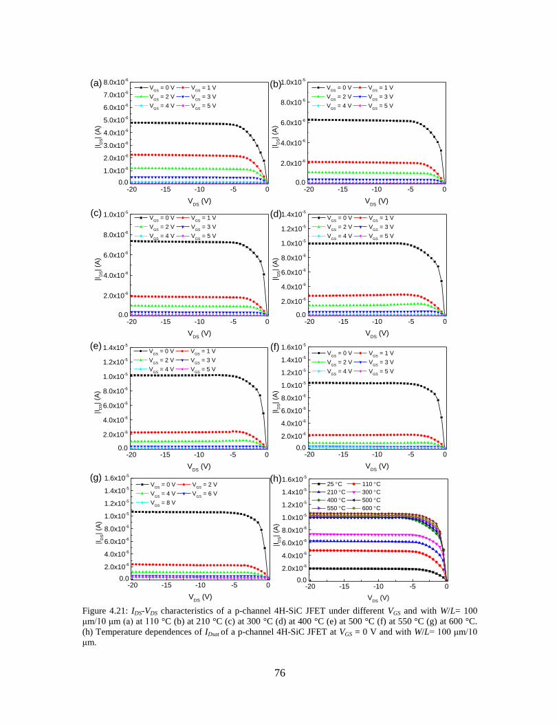
76
Figure 4.21: IDS-VDS characteristics of a p-channel 4H-SiC JFET under different VGS and with W/L= 100
μm/10 μm (a) at 110 °C (b) at 210 °C (c) at 300 °C (d) at 400 °C (e) at 500 °C (f) at 550 °C (g) at 600 °C.
(h) Temperature dependences of IDsat of a p-channel 4H-SiC JFET at VGS = 0 V and with W/L= 100 μm/10
μm.
(a)
(c)
(e)
(b)
(d)
(f)
(g) (h)
-20 -15 -10 -5 00.0
2.0x10⁻⁶
4.0x10⁻⁶
6.0x10⁻⁶
8.0x10⁻⁶
1.0x10⁻⁵
1.2x10⁻⁵
1.4x10⁻⁵
1.6x10⁻⁵
|ID
S| (A
)
VDS
(V)
25 C 110 C
210 C 300 C
400 C 500 C
550 C 600 C
-20 -15 -10 -5 00.0
1.0x10⁻⁶
2.0x10⁻⁶
3.0x10⁻⁶
4.0x10⁻⁶
5.0x10⁻⁶
6.0x10⁻⁶
7.0x10⁻⁶
8.0x10⁻⁶
|I D
S| (A
)
VDS
(V)
VGS
= 0 V VGS
= 1 V
VGS
= 2 V VGS
= 3 V
VGS
= 4 V VGS
= 5 V
-20 -15 -10 -5 00.0
2.0x10⁻⁶
4.0x10⁻⁶
6.0x10⁻⁶
8.0x10⁻⁶
1.0x10⁻⁵
|I D
S| (A
)
VDS
(V)
VGS
= 0 V VGS
= 1 V
VGS
= 2 V VGS
= 3 V
VGS
= 4 V VGS
= 5 V
-20 -15 -10 -5 00.0
2.0x10⁻⁶
4.0x10⁻⁶
6.0x10⁻⁶
8.0x10⁻⁶
1.0x10⁻⁵
|I D
S| (A
)
VDS
(V)
VGS
= 0 V VGS
= 1 V
VGS
= 2 V VGS
= 3 V
VGS
= 4 V VGS
= 5 V
-20 -15 -10 -5 00.0
2.0x10⁻⁶
4.0x10⁻⁶
6.0x10⁻⁶
8.0x10⁻⁶
1.0x10⁻⁵
1.2x10⁻⁵
1.4x10⁻⁵
|I D
S| (A
)
VDS
(V)
VGS
= 0 V VGS
= 1 V
VGS
= 2 V VGS
= 3 V
VGS
= 4 V VGS
= 5 V
-20 -15 -10 -5 00.0
2.0x10⁻⁶
4.0x10⁻⁶
6.0x10⁻⁶
8.0x10⁻⁶
1.0x10⁻⁵
1.2x10⁻⁵
1.4x10⁻⁵
|I D
S| (A
)
VDS
(V)
VGS
= 0 V VGS
= 1 V
VGS
= 2 V VGS
= 3 V
VGS
= 4 V VGS
= 5 V
-20 -15 -10 -5 00.0
2.0x10⁻⁶
4.0x10⁻⁶
6.0x10⁻⁶
8.0x10⁻⁶
1.0x10⁻⁵
1.2x10⁻⁵
1.4x10⁻⁵
1.6x10⁻⁵
|I D
S| (A
)
VDS
(V)
VGS
= 0 V VGS
= 1 V
VGS
= 2 V VGS
= 3 V
VGS
= 4 V VGS
= 5 V
-20 -15 -10 -5 00.0
2.0x10⁻⁶
4.0x10⁻⁶
6.0x10⁻⁶
8.0x10⁻⁶
1.0x10⁻⁵
1.2x10⁻⁵
1.4x10⁻⁵
1.6x10⁻⁵
|I D
S| (A
)
VDS
(V)
VGS
= 0 V VGS
= 2 V
VGS
= 4 V VGS
= 6 V
VGS
= 8 V

77
However, there are some non-ideal behaviors of the device when increasing the
operating temperature. Figure 4.22 shows the IDS-VGS curves under a drain-to-source -20
V bias and at incremental temperatures up to 600 °C. The saturation currents exhibit a
kink effect around VGS of 0 to 0.5 V at temperature greater than 25 °C, and the IDsat at VGS
< 0 has the a smaller degree of increase or remains roughly the same when increasing the
temperature, unlike the IDsat at VGS = 0 V. The whole JFET can be divided into many 2D
JFETs, and the whole saturation current is the superposition of the current from these 2D
transistors. Therefore, if these devices exhibit different threshold voltages, then they will
have different saturation current for same VGS. A clear definition of gate area with
uniform doping is more difficult to achieve if the gate is ion implanted rather than mesa
etched on the epitaxial layers due to the 4-degree-off SiC wafer and thin film which
might contribute the kink effect of saturation current in the IDS-VGS curves.
Figure 4.22: |IDS|-VGS characteristics of a p-channel 4H-SiC JFET under VDS = -20 V and with W/L= 100
μm/10 μm at different temperatures.
The threshold voltages increased from 4.39 V at 25 °C to 5.71 V at 600 °C,
respectively, and are approximately shifted with a rate of +2.1 mV/ °C, as shown in
Figure 4.23. The temperature dependencies of the estimated transconductance and the
intrinsic gain of the p-channel JFET at VGS = 0 V are shown in Figure 4.24. Compared
with the transconductance value of room temperature, the transconductance at VGS = 0 V
and 600 °C is increased to 0.037 μS/μm leading to intrinsic gain increases of 55.4 dB.
The intrinsic gain of the JFET does not have monotonic temperature dependence but the
overall tendency is to decrease with increasing temperature. The complete electrical
properties of n-channel raised gate 4H-SiC JFET are listed and summarized in Table 4.5.
Compared with the performance of the n-channel raised gate JFET described in Chapter
3, the p-channel buried gate JFET has a small gm and IDsat/Ioff and the Ron is quite large.
The gm of n-channel JFET is 500 times higher than the p-channel device at 25 and
reduces to 20 times at 600 °C owing to the increased degree of ionization of holes. For
the amplifier application, the saturation current could be matched by carefully designing
the device geometry. Besides, it seems that the raised gate which used in-situ doping
0 2 4 6 8 1010
-9
10-8
10-7
10-6
10-5
|ID
S| (A
)
VGS
(V)
T = 25 C T = 110 C
T = 210C T = 300 C
T = 400 C T = 500 C
T = 550 C T = 600 C

78
during the epitaxial films growth yield better quality than ion-implanted gate [26].
Figure 4.23: Temperature dependence of threshold voltage of a p-channel 4H-SiC JFET with W/L= 100
μm/10 μm.
Figure 4.24: Temperature dependence of transconductance and intrinsic gain of of a p-channel 4H-SiC
JFET with W/L= 100 μm/10 μm.
0 100 200 300 400 500 6004.2
4.4
4.6
4.8
5.0
5.2
5.4
5.6
5.8
VT (
V)
Temperature (C)
0 100 200 300 400 500 6000.00
0.01
0.02
0.03
0.04
0.05
gm
gmr
o
Temperature (C)
gm (
S/
m)
100
200
300
400
500
600
700
800
900
gmr o

79
Temperature
(°C) VT (V)
gm
(µS/µm)
Ron (Ω
cm2)
ro (Ω) λ (mV-1
) gmro IDsat/Ioff
25 4.39 0.009 21.8 2.36×10⁸ 2.28 208.3 305
110 4.50 0.021 7.5 1.26×10⁸ 1.71 268.2 296
210 4.50 0.028 4.4 1.26×10⁸ 1.29 351.8 196
300 4.58 0.032 3.4 1.28×10⁸ 1.09 411.4 114
400 4.90 0.041 2.7 1.29×10⁸ 7.83 521.8 71
500 5.10 0.040 2.5 1.30×10⁸ 7.71 516.0 127
550 5.35 0.039 2.5 1.76×10⁸ 5.54 682.1 77
600 5.71 0.037 2.4 1.58×10⁸ 6.00 591.5 34
Table 4.5: Extracted parameters of p-channel buried gate 4H-SiC JFET with W/L= 100 μm/10 μm at
various temperatures. gm, Ron, ro , λ and gmro is based on VGS = 0 V. IDsat/Ioff is the ratio of current at VGS = 0
V to current at VGS = 7 V.
4.7 Summary
The low voltage normally on complementary JFETs with buried gate
configuration using 4H-SiC are proposed. The contact resistances between Ni/Ti/Al/TiW
metal stacks and n- and p-type 4H-SiC are 3.38×10⁻⁴
and 1.07×10⁻³
Ω cm2, respectively.
The channel conductivity is not fully functional with applied gate bias for n-JFET. The
threshold voltage at 25 °C is 4.39 V with low transconductance of 0.009 µS/µm. As the
temperature increases, the threshold voltage shifts with the rate of 2.1 mV/ °C. The
transconductance is increased to 0.037 µS/µm with intrinsic gain of 591.5 at 600 °C due
to the increased hole ionization. However, the kink problem at IDS-VGS curves and large
on-resistance need to be improved for the practical use of a p-channel 4H-SiC JFET.
4.8 Reference
[1] R. Behzad, Design of analog CMOS integrated circuits:McGraw-Hill
International Edition, 2001.
[2] P. R. Gray, P. J. Hurst, R. G. Meyer, and S. H. Lewis, Analysis and design of
analog integrated circuits: Wiley, 2008.
[3] P. G. Neudeck, R. S. Okojie, and L.-Y. Chen, "High-temperature electronics-a
role for wide bandgap semiconductors?," Proceedings of the IEEE, vol. 90, pp.
1065-1076, 2002.

80
[4] M. R. Werner and W. R. Fahrner, "Review on materials, microsensors, systems
and devices for high-temperature and harsh-environment applications," IEEE
Transactions on Industrial Electronics, vol. 48, pp. 249-257, 2001.
[5] H. K. Alexander Schmidt, Rainer Kokozinski, "Enhanced high temperature
performance of PD-SOI MOSFETS in analog circuits using reverse body
biasing," IMPAS Conference & Exhibition on High Temperature Network (HiTEN
2013), 2013.
[6] W.-C. Lien, D.-S. Tsai, D.-H. Lien, D. G. Senesky, J.-H. He, and A. P. Pisano,
"4H–SiC Metal–Semiconductor–Metal Ultraviolet Photodetectors in Operation of
450 °C," 2012.
[7] D. Clark, E. P. Ramsay, A. Murphy, D. A. Smith, R. Thompson, R. Young, J. D.
Cormack, C. Zhu, S. Finney, and J. Fletcher, "High temperature silicon carbide
CMOS integrated circuits," in Materials Science Forum, 2011, pp. 726-729.
[8] P. G. Neudeck, D. J. Spry, L.-Y. Chen, G. M. Beheim, R. S. Okojie, C. W. Chang,
R. D. Meredith, T. L. Ferrier, L. J. Evans, and M. J. Krasowski, "Stable Electrical
Operation of 6H–SiC JFETs and ICs for Thousands of Hours at 500," IEEE
Electron Device Letters, vol. 29, pp. 456-459, 2008.
[9] L. Lanni, R. Ghandi, B. G. Malm, C. Zetterling, and M. Ostling, "Design and
characterization of high-temperature ECL-based bipolar integrated circuits in 4H-
SiC," IEEE Transactions on Electron Devices, vol. 59, pp. 1076-1083, 2012.
[10] H. Okumura, M. Okamoto, K. Fukuda, M. Iijima, and T. Nagano, "Controlling
Characteristics of 4H-SiC (0001) p-Channel MOSFETs Fabricated on Ion-
Implanted n-Well," in Materials Science Forum, 2012, pp. 781-784.
[11] S. Seshadri, G. Eldridge, and A. Agarwal, "Comparison of the annealing behavior
of high-dose nitrogen-, aluminum-, and boron-implanted 4H–SiC," Applied
Physics Letters, vol. 72, pp. 2026-2028, 1998.
[12] A. B. Horsfall, D. Clark, N. G. Wright, L. C. Martin, E. Ramsay, A. Murphy, R.
Thompson, D. A. Smith, R. Young, and J. D. Cormack, "Charge Pumping
Analysis of Monolithically Fabricated 4H-SiC CMOS Structures," in Materials
Science Forum, 2013, pp. 891-894.
[13] D. Clark, E. P. Ramsay, A. Murphy, D. A. Smith, R. Thompson, R. Young, J. D.
Cormack, and S. Finney, "High Temperature Digital and Analogue Integrated
Circuits in Silicon Carbide," in Materials Science Forum, 2013, pp. 1065-1068.
[14] J.-S. Chen and K. T. Kornegay, "Design of a process variation tolerant CMOS
opamp in 6H-SiC technology for high-temperature operation," , IEEE
Transactions on Circuits and Systems I: Fundamental Theory and
Applicationsvol. 45, pp. 1159-1171, 1998.
[15] H. Habib, N. G. Wright, and A. B. Horsfall, "Effects of Process Variations on
Silicon Carbide Devices for Extreme Environments," in Materials Science Forum,
2011, pp. 401-404.
[16] S. M. Sze and K. K. NG, Physics of semiconductor devices: Wiley, 2007.
[17] T. Ayalew, "SiC Semiconductor Devices Technology, Modeling, and Simulation
", Technical University of Vienna, 2004.
[18] C.-M. Zetterling, Process technology for silicon carbide devices: IET, 2002.

81
[19] M. Lades, W. Kaindl, N. Kaminski, E. Niemann, and G. Wachutka, "Dynamics of
incomplete ionized dopants and their impact on 4H/6H-SiC devices," , IEEE
Transactions on Electron Devices, vol. 46, pp. 598-604, 1999.
[20] S. Greulich-Weber, M. Feege, J.-M. Spaeth, E. Kalabukhova, S. Lukin, and E.
Mokhov, "On the microscopic structures of shallow donors in 6H SiC: studies
with EPR and ENDOR," Solid State Communications, vol. 93, pp. 393-397, 1995.
[21] M. Laube, F. Schmid, G. Pensl, G. Wagner, M. Linnarsson, and M. Maier,
"Electrical activation of high concentrations of N+ and P+ ions implanted into
4H–SiC," Journal of Applied Physics, vol. 92, pp. 549-554, 2002.
[22] A. A. Stephen E. Saddow, Advances in Silicon Carbide Processing and
Applications, Artech House, Inc., 2004.
[23] K. Tone, J. H. Zhao, L. Fursin, P. Alexandrov, and M. Weiner, "4H-SiC
normally-off vertical junction field-effect transistor with high current density,"
IEEE Electron Device Letters, vol. 24, pp. 463-465, 2003.
[24] M. V. Rao, J. B. Tucker, M. Ridgway, O. Holland, N. Papanicolaou, and J.
Mittereder, "Ion-implantation in bulk semi-insulating 4H–SiC," Journal of
Applied Physics, vol. 86, pp. 752-758, 1999.
[25] C. Chang, Y. Fang, and S. Sze, "Specific contact resistance of metal-
semiconductor barriers," Solid-State Electronics, vol. 14, pp. 541-550, 1971.
[26] D. Planson, C. Raynaud, M. Lazar, D. Tournier, M. Soueidan, and D. M. Nguyen,
"Process Optimization for High Temperature SiC Lateral Devices," in Materials
Science Forum, 2009, pp. 585-588.

82
Chapter 5
Conclusion and Future Work
5.1 Contributions of This Work
Integrated SiC UV sensing chips are promising candidates for the real time
condition monitoring of power systems and for space exploration. This dissertation
addresses the two building blocks of the sensing system, namely UV sensor and transistor.
Conventional SiC pn photodiodes show stable performance and high responsivity
up to 300 °C. However, the extra thin film deposition for the specific junction doping
concentration might hinder the development of an integrated sensing chip. An integrated
compatible SiC metal-semiconductor-metal UV sensor has been designed, fabricated and
characterized. High temperature tests confirm that the MSM PD can work up to 400 °C
and possibly extend the temperature to 450 °C. The speed measurement was conducted at
400 °C and the MSM photodetector shows a fast response time, able to detect the flicker
frequency of flame in combustion engine [1].
To further explore the possibility of integrating the whole UV sensing system, a
junction field effect transistor was chosen to evaluate the ability to design the
transimpedance amplifier, which can convert photocurrent generated from MSM PD to
voltage. While most SiC JFETs for low voltage amplifier application use 6H-SiC, few
works discuss the performance of low power JFET using 4H-SiC [2]. Most device
research on 4H-SiC target the high power electronics, such as vertical JFET, MOSFET
and BJT. Given the largest SiC wafer manufacture, Cree Inc., has announced to shut
down the production line of 6H-SiC, it is worth investigating the performance of 4H-SiC
JFET at elevated temperatures. A lateral, depletion mode, low voltage n-channel 4H-SiC
JFET has been design, fabricated and completely characterized in the temperature range
of 25 to 600 °C. High transconductance and on/off drain saturation current, decent output
resistance and low on-resistance suggest that 4H-SiC is suitable for the high temperature
electronics. The complete model of the SPICE DC level 1 for n-channel raised 4H-SiC
JFET has been developed which is beneficial for the future analog circuit design.
Finally, the complementary JFET was proposed in order to add the flexibility to
amplifier circuit design and increase the bandwidth of the amplifier. The first prototype
of cJFET is designed using a buried gate configuration in order to reduce the number of
fabrication steps. The fabricate n-channel buried gate JFET has the problem of being
completely turn-off even at a gate bias of 10 V. The p-channel buried gate JFET was
characterized up to 600 °C. The transconductance at room temperature is fairly low due

83
to the low mobility and low degree of ionization of holes. As the ambient temperature
increased to 600 C, more than 90 % of acceptor carries were ionized and thus boost the
transconductance value of p-channel JFET.
5.2 Integrated SiC Sensor Design Challenges
Many challenges must be addressed for further integrated SiC sensor development.
The lists below highlight some of the fundamental problems.
Semiconductor device modeling for JFET. The simulation model built with
Synopsys Sentaurus in this work cannot completely match the measured data of both
raised and buried gate configurations. More specifically, the simulated device exhibits the
ultra low leakage current (< 10-15
A) and small subthreshold swing (~74 mV/dec),
suggesting that more non-ideal parameters should be taken into account in the future
TCAD simulations.
Fabrication complexity. This includes the challenge of precise time-etched
process to define the device structure, usually the thickness of the channel. This is crucial
for fabricating the complementary devices, which usually entail multiple etching
processes of epitaxial layers. Failure to control the etch thickness of SiC will result in
different electrical properties than the designed value. Furthermore, a stable annealing
cap is required for activating the implanted p-type dopants with an annealing temperature
greater than 1500 °C.
Complementary Device Geometry. It seems that the raised gate JFET has a
greater chance of success and more stable performance at extreme high temperature, most
likely due to the epitaxially grown gate having better crystallinity than the implanted gate.
However, it is very challenging to integrate the complementary devices if both of them
are raised gate configuration. One possible solution would be to use the back gate
configuration [3, 4]. The advantage of this configuration is using the epitaxially grown
gate and also reducing the chance of using ion implantation to facilitate the Ohmic
contact between the contact metal and the source/drain area. The disadvantage is that this
geometry requires many steps in the precise time-etched process described earlier.
Metallization. In order to integrate the MSM UV sensor and JFET into the same
fabrication process, it is important to have the contact metal forming an Ohmic contact
with n+ or p
+ area for JFET and Schottky contact with low doped film for MSM PDs at
the same time. Currently, there are very few candidates able to achieve this requirement
with high thermal stability for high temperature operation. A novel tungsten-nickel alloy
seems to show promising preliminary results for both n- and p-type 4H-SiC [5]. More
studies on metallization are needed in the future.
5.3 Reference

84
[1] D. M. Brown, E. Downey, J. Kretchmer, G. Michon, E. Shu, and D. Schneider,
"SiC flame sensors for gas turbine control systems," Solid-State Electronics, vol.
42, pp. 755-760, 1998.
[2] A. B. Horsfall, N. G. Wright, H. K. Chan, J. P. Goss, and R. C. Stevens,
"Reliability Evaluation of 4H-SiC JFETs Using IV Characteristics and Low
Frequency Noise," in Materials Science Forum, 2013, pp. 934-937.
[3] S. Zappe, M. Leone, F. Yang, and E. Obermeier, "Characterisation of silicon
carbide JFETs with respect to microsystems for high temperature applications,"
Microsystem Technologies, vol. 3, pp. 134-138, 1997.
[4] F. McLean, C. Tipton, J. McGarrity, and C. Scozzie, "Modeling the electrical
characteristics of n‐channel 6H–SiC junction‐field‐effect transistors as a function
of temperature," Journal of Applied Physics, vol. 79, pp. 545-552, 1996.
[5] R. S. Okojie, L. J. Evans, D. Lukco, and J. P. Morris, "A Novel Tungsten–Nickel
Alloy Ohmic Contact to SiC at 900," IEEE Electron Device Letters, vol. 31, pp.
791-793, 2010.