Embed Size (px)
Citation preview

ADS 2012 Circuit Simulation Techniques (v.2 - April 2013)
© Copyright Agilent Technologies 2013
LAB EXERCISE 3
Harmonic Balance Techniques
Topics: Harmonic Balance simulations are covered including swept variables, 2-tone simulations, equations for HB data, compression, and IP3.
Audience: Engineers who have a basic working knowledge of ADS or have completed the prerequisite course.
Prerequisites: Completion of lab exercises 1 and 2 of this course. Also, completion of Workspaces and Simulation Tools or equivalent experience, including basic circuit design concepts.
Objectives: Be able to set up and run HB simulations for various tests.

Lab 3: HB Techniques
Copyright 2013 Agilent Technologies
2
Table of Contents: Lab 3
1. FET amplifier design 3
2. Basic HB 1‐Tone Simulation 4
3. Functions and Equations for Input Power and Zin 5
4. Gain Compression using XDB 8
5. Sweep Input Power and Bias Voltage 9
6. Output Power, Gain, and Power Sweep with a Slider 11
7. Two‐tone HB Simulation with variables 14
8. Spectrum and Mix table 15
9. OPTIONAL: IP3 Simulation (Third Order Intercept Point) 17

Lab 3: HB Techniques
Copyright 2013 Agilent Technologies
3
Lab 3: Harmonic Balance Techniques
NOTE: In the last lab, this design had a small signal gain of about 15 dB and was stable over a wide band. This will be the starting point for large signal simulation, including 2-tone, gain, TOI, and optimizing PAE and power delivered to a 50 Ohm load (optional).
1. FET amplifier design
a. In your My_FET_AMP workspace, click File > Open > Schematic and select the S_Params_Zmatch (schematic view) and click OK.
b. When the design appears, use File > Save As and save the cell with a new name, HB_testing, as shown here. Then delete the input termination, DC and S-parameter controller, and the two display templates.
c. You design should look like the one shown here. If so, save it again – it is now ready to be set up for Harmonic Balance.

Lab 3: HB Techniques
Copyright 2013 Agilent Technologies
4
2. Basic HB 1-Tone Simulation
REVIEW NOTE – From past experience or the prerequisite ADS 2012 course, you learned how to set up a 1-tone HB simulation, plot the output spectrum and use brackets to isolate desired tones such as the fundamental of Vout = [1]. You also wrote a simple gain equation and swept RF power and frequency. This step will combine all those skills as a review and starting point for the techniques that follow.
a. Insert a P_1Tone source and VAR.
b. Declare two variables: RF_freq= 7GHz and RF_pwr = 10.
c. Set the source Freq=RF_freq and the power P= dbmtow(RF_pwr).
d. Insert a Harmonic Balance controller and set Freq= RF_freq.
e. Label V_in and V_out as shown here.
f. Select the VAR and use Edit > Properties to make the font larger. This is useful when you want specific components to be easily seen.
g. Save the design.
Lab 3: HB Techniques
Copyright 2013 Agilent Technologies
5
h. Run the simulation.
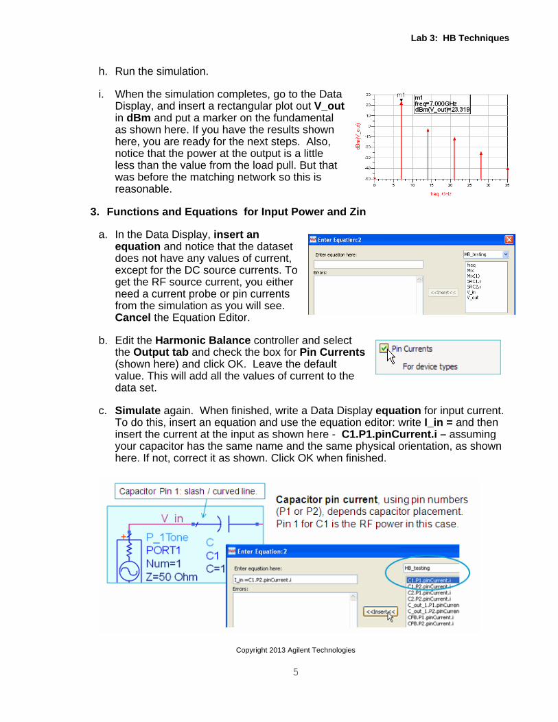
i. When the simulation completes, go to the Data Display, and insert a rectangular plot out V_out in dBm and put a marker on the fundamental as shown here. If you have the results shown here, you are ready for the next steps. Also, notice that the power at the output is a little less than the value from the load pull. But that was before the matching network so this is reasonable.
3. Functions and Equations for Input Power and Zin
a. In the Data Display, insert an equation and notice that the dataset does not have any values of current, except for the DC source currents. To get the RF source current, you either need a current probe or pin currents from the simulation as you will see. Cancel the Equation Editor.
b. Edit the Harmonic Balance controller and select the Output tab and check the box for Pin Currents (shown here) and click OK. Leave the default value. This will add all the values of current to the data set.
c. Simulate again. When finished, write a Data Display equation for input current. To do this, insert an equation and use the equation editor: write I_in = and then insert the current at the input as shown here - C1.P1.pinCurrent.i – assuming your capacitor has the same name and the same physical orientation, as shown here. If not, correct it as shown. Click OK when finished.

Lab 3: HB Techniques
Copyright 2013 Agilent Technologies
6
d. On screen, insert your cursor at the end of the equation and add the bracketed [1] at the end so that it’s the current at 7 GHz.
The equation should be as shown here – you will use this to calculate impedance and power.
e. Write an equation for input impedance Zin using V_in and I_in at 7 GHz as shown here. This is the calculated input impedance looking into the amplifier.
f. Write an equation for RF input power (dBm) using the node voltage (wire label): V_in as shown here.
g. Write one more equation to calculate average delivered input power using the node voltage Vin and the input current using equation I_in:
NOTE : Using 0.5 gives the average of the peak value, the conj function converts the complex current to its conjugate because V&I must be in phase to dissipate power, and + 30 converts the value to dBm (same as dividing by 0. 001).
h. Insert a list of all four equations as shown here:
Notice that Z_in is not 50 Ohms but is a reasonable value. Also, notice that both power calculations are different and not exactly 10 dBm. This is because the P_del_dBm uses the current and voltage and RF_dbm uses only the voltage with the dBm function. Next, you will see why this happens.

Lab 3: HB Techniques
Copyright 2013 Agilent Technologies
7
i. Edit (double-click) the RF_dbm equation and click on the Functions Help button. Then select the Measurement Expression Function (alphabetical) scroll down to the dbm ( ) function as shown here. Read the information on this function and notice that the returned value is for a 50 Ohm Zo. This means that the value of your equation is not correct. This is important when using functions in equations – you should read about the function arguments.
j. Close the Help and close the equation editor.
k. Insert your cursor directly in the RF_dbm equation and type in a comma (,) and then type in Z_in as the second argument. You should see that the value changes to match the value from the P_del_dBm equation which is correct.
Now you should have a good idea how to use ADS measurement functions and how to use Function Help to learn about the function arguments if necessary.
l. Save and close the Data Display window. Save the schematic but keep it open.

Lab 3: HB Techniques
Copyright 2013 Agilent Technologies
8
4. Gain Compression using XDB
a. In the schematic, use the Save As command and create a new cell / schematic: HB_compression.
You will modify the schematic and use the XDB simulation controller. It is a special Harmonic Balance simulation controller for measuring gain compression.
b. In the new schematic, deactivate the HB controller.
c. Go to the Simulation-XDB palette and insert the XDB controller. Edit the controller on screen so that Freq[1] and GC input and output frequencies = RF_freq as shown. The parameter GC_XdB = 1 means that the test will be for 1 dB Gain Compression. If you wanted 3 or 6 dB compression, you could change the value.
d. Use Simulate > Simulation Settings and change the dataset name to HB_XDB. Then Simulate.
e. When the data display opens, insert a list of inpwr and outpwr. Then edit directly on the list by inserting a bracketed one [1] after each data item as shown. If desired, title the plot as shown. You just performed a 1 dB gain compression test in only a few seconds! Also, use Plot Options to title the plot if you have time. This makes it easy read your data and plots.

Lab 3: HB Techniques
Copyright 2013 Agilent Technologies
9
The result of the Gain Compression test (XDB) shows that 1 dB of compression occurs when the input power is almost 8 dBm. Next, you will sweep RF power and bias voltage to see the effects of a draining battery on output power and gain.
5. Sweep Input Power and Bias Voltage
a. Edit the VAR and add another variable; VDS = 3 as shown here. This is the battery voltage that will be the outer sweep.
b. Set the drain DC source = VDS as shown.
c. Go to any Simulation palette and insert a Parameter Sweep.
d. Set the SweepVar = “VDS” - if you edit on-screen you will have to type the quotes. If you edit the Parameter Sweep do not type in the quotes (they will appear automatically).
e. Set the Start =3, Stop = 1, and Step = 0.5.
f. Specify the simulation controller instance name – here it is: “HB1”.
g. Activate and Edit the HB controller. In the Sweep tab, specify RF_pwr from 0 to 10 with step = 1 (This was covered in the prerequisite course). Go to the Display tab and check the boxes for SweepVar, Start, Stop, Step. Click OK.
This is the inner sweep. At each value of RF power, all the values of VDS will be swept. This is important for understanding how to operate on your data in the Data Display after simulation.

Lab 3: HB Techniques
Copyright 2013 Agilent Technologies
10
h. Delete the wire at V_out – the node label (V_out) will disappear with it. Then go to the Probe Components palette and insert a current probe connected between the output capacitor and the Term at the output.
i. Use the NAME icon and rename V_out again as shown here.
j. Set the probe instance name to I_OUT on-screen.
k. Finally, deactivate the XDB controller and check your design – it should have the values shown here. If desired, use F5 to move text and save the design.
l. Use Simulate > Simulation Setup – check the boxes to use the cell name for the dataset and display. This will make it easier in the next steps. Go ahead and Simulate.
Lab 3: HB Techniques
Copyright 2013 Agilent Technologies
11
6. Output Power, Gain, and Power Sweep with a Slider
Now, you need to write two equations for output power. Remember that you can always copy and paste equations from one Data Display to another so you don’t have to re-write them every time. You can also create a Data Display of equations that you can copy to a workspace as needed.
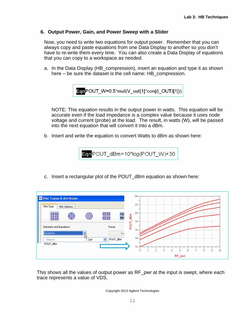
a. In the Data Display (HB_compression), insert an equation and type it as shown here – be sure the dataset is the cell name: HB_compression.
NOTE: This equation results in the output power in watts. This equation will be accurate even if the load impedance is a complex value because it uses node voltage and current (probe) at the load. The result, in watts (W), will be passed into the next equation that will convert it into a dBm.
b. Insert and write the equation to convert Watts to dBm as shown here:
c. Insert a rectangular plot of the POUT_dBm equation as shown here:
This shows all the values of output power as RF_pwr at the input is swept, where each trace represents a value of VDS.

Lab 3: HB Techniques
Copyright 2013 Agilent Technologies
12
d. Edit the plot and select the POUT_dBm trace and click Trace Options as shown here. Then check the box (at the bottom) to Display Label and click OK as needed. This is how you can label traces with the swept values.
e. Marker Slider: Use the command Insert > Slider and insert the slider.
f. When the dialog appears, select VDS as the swept data to add, as shown here. Then click the Add button - it will appear in both fields.
g. Click OK and the slider will be created as you see here.
The next step is to use it in your plot.

Lab 3: HB Techniques
Copyright 2013 Agilent Technologies
13
The slider creates an equation that is added to your dataset. You use the equation to index the data you want the marker to display as a trace – as you will see.
h. Edit your plot of POUT_dBm and select the Equations drop down, as shown here, and Add the marker index. Then select the equation and click Trace Options – select Trace Expression – then modify the trace expression as shown here to be: POUT_dBm [m1_VDS_index,::] and click OK as needed.
i. Your plot should look similar to the one shown here: move the marker on the slider and the plot trace should update. You can change the trace color or thickness. You can also change the marker trace color to match the updated trace using Trace Options on the slider trace if you have time.
NOTE: The double colon (::) you added to the trace expression creates the trace over all the swept values – without it, you would only get the slider readout value.
j. Save your work and close the Data Display – but keep the schematic open.

Lab 3: HB Techniques
Copyright 2013 Agilent Technologies
14
7. Two-tone HB Simulation with variables
a. Save the schematic /cell as: HB_2_tone.
b. Edit the VAR and set RF_pwr = 7 (power before 1dB compression) and Add a variable: spacing = 5 MHz.
NOTE on units in VARs – If you set units here do not set them anywhere else or they may multiply in the simulation.
c. Delete the P_1Tone source and replace it with a P_nTone source. Then edit the source and add another Freq and P parameter. Set Freq [1] and Freq [2] as shown here (+/- the spacing variable / 2). Also set P[1] and P [2] = RF_pwr.
d. Edit the Harmonic Balance controller and Add another frequency: Freq[2]. Specify the values shown here, using RF_freq +/- the spacing variable / 2. Also, set the Order = 3 for both frequencies and set MaxOrder = 6. In this case, the two RF tones are spaced 5 MHz apart (typical channel spacing).
e. Remove the RF_pwr sweep from the controller by erasing it on-screen (values are blank) or remove it in the dialog and display tab.

Lab 3: HB Techniques
Copyright 2013 Agilent Technologies
15
f. Verify that your circuit looks like the one shown here – you can delete the Parameter Sweep and XDB controller.
8. Spectrum and Mix table
a. Run the simulation.
b. Plot the spectrum of V_out in dBm. Notice that you must zoom in on the plot or change the X axis scaling to see the closely spaced tones. Try both of these methods quickly because the next step shows a better technique using equations.
c. Insert a List of Mix as shown here. With two RF (freq) tones, you get two Mix columns and the resulting products. With Order = 3 and MaxOrder = 6, you can see how the index values correspond to the frequencies.

Lab 3: HB Techniques
Copyright 2013 Agilent Technologies
16
d. Create a matrix with vectors (index values) to the desired tones: 4 closely spaced tones. To do this, write the tones equation shown here. This equation creates a matrix using the square brackets. Within the brackets are curly braces with index values for the mix table. In this case, the number 1 represents the RF tone with spacing. Zero means that no other tone is desired (same as DC), and 2 represents two times the RF tone.
e. In your plot of dBm(Vout), insert your cursor into the trace label on the Y-axis. The trace expression will rotate so you can edit it. Change it as shown here to: dBm(mix(V_out, tones)). Next you will change the trace type to spectral.
f. Double-click (edit) the trace and use Trace Options > Trace Type to change the trace type to Spectral – now you can clearly see the tones you specified.

Lab 3: HB Techniques
Copyright 2013 Agilent Technologies
17
g. Look at your List of Mix data (Mix table) and scroll through it to find the index values shown here. Compare the list of index values to your plot. With markers, you can see how the mix values produce the tones from your equation. This is how Harmonic Balance data can be accessed and controlled using equations.
h. Save the Data Display and the schematic. If you are not doing the optional step,
you can close them also.
9. OPTIONAL: IP3 Simulation (Third Order Intercept Point)
a. In the same schematic, go to the Harmonic Balance palette- insert two IP3out measurement equations (icon shown here): one for the upper and one for the lower spaced tones. Many measurements require two-tones so name the equations upper_IP3 and lower_IP3 as shown here.
b. Change default node name (vout) to V_out (your node labels).
c. Set the index values in curly braces { } to those shown here – you will see where these come from after the simulation by inserting a Mix table (in a following step).
d. The impedance argument, 50 ohms, is OK here because we have matched the output to 50 ohms.
e. Save the design and run the simulation.

Lab 3: HB Techniques
Copyright 2013 Agilent Technologies
18
a. In the Data Display, list the two measurement equations for IP3 as shown here.
These are the values that indicate when the 3rd order product would intercept the fundamental if the amplifier remained linear as the input power increased.
b. Remove the independent variable (freq) by using Plot Options – uncheck the box Display Indep Data as shown. Here the amplifier TOI values appear reasonable and almost symmetrical.
c. Save and close the schematic and data display.
a. When finished, save and close all your work.
After completing all of the steps in this lab, you should have acquired a reasonable amount of skill using Harmonic Balance and HB data. The techniques shown here can be applied to many other types of circuits.
END OF LAB EXERCISE.