Embed Size (px)
Citation preview

Hardware prototyping of FBMC/OQAM basebandfor 5G mobile communicationJeremy Nadal∗, Charbel Abdel Nour∗, Amer Baghdadi∗, Hao Lin†
∗Institut Mines-Telecom; Telecom Bretagne; Lab-STICC, Technopole Brest-Iroise, 29238 Brest, France†Orange Labs, 4 rue du Clos Courtel, 35512 Cesson Sevigne, France
Email: {jeremy.nadal,charbel.abdelnour,amer.baghdadi}@telecom-bretagne.eu, [email protected]
Abstract—Embedded systems in the field of digital commu-nications are becoming increasingly diversified and complex.This trend is being confirmed with the emergence of manynew application scenarios for mobile communication systemsbeyond 2020. In this context, rapid prototyping experiencesare of high interest for performance validation and proof-of-concept of the diverse proposed communication techniques. Inthis paper, we present a new design and prototyping experience ofan advanced communication system based on filter-bank multi-carrier (FBMC) modulation. This modulation is being studiedand considered nowadays by recent research projects as a keyenabler for the future flexible 5G air interface. The paperillustrates the complete design and prototyping flow from al-gorithm specification to on-board validation and demonstration.The proposed prototype enables to illustrate and evaluate theperformance of this new waveform compared to state-of-the-artOFDM-based systems.
I. INTRODUCTION
Next generation mobile communication systems are fore-seen to provide ubiquitous connectivity and seamless servicedelivery in all circumstances. There are forecasts of a total of50 billion connected devices by 2020 [1]. This huge expectednumber of devices and the coexistence of human-centricand machine-type applications will lead to a large diversityof communication scenarios and characteristics [2]. In thiscontext, many advanced communication techniques are underinvestigation. Each of these techniques is typically suitable fora subset of the foreseen communication scenarios.
However, the proposed new communication techniques areoften studied and analysed at the algorithmic level consideringmainly the quality of the communication link, i.e. qualityof service. Although this remains as one of the main KeyPerformance Indicators (KPI), the related hardware and energyefficiencies are becoming increasing crucial requirements forfuture mobile terminals and networks.
Thus, the availability of new rapid design, validation flowsand related prototyping experiences are of high interest forperformance validation and proof-of-concept of the diverseproposed communication techniques. In this context, this paperpresents a new design and prototyping experience of anadvanced communication system based on filter-bank multi-carrier (FBMC) modulation. This modulation is being studiedand considered nowadays by recent research projects as a keyenabler for the future flexible 5G air interface [3]. It exhibitsbetter spectrum shape compared to the traditional OFDM(Orthogonal Frequency-Division Multiplexing) and enablesbetter spectrum usage and mobility support.
The paper considers the recent FBMC/OQAM (OffsetQuadrature Amplitude Modulation) technical component pro-posed in the framework of the METIS project (the European
flagship 5G project) [4]. It illustrates the complete designand prototyping flow, including: (1) algorithm simplificationand optimisation, (2) architecture exploration, (3) hardwareimplementation, and (4) on-board validation and demonstra-tion. To the best of the authors knowledge, this constitutesthe first published design and prototyping experience relatedto this new technical component. The proposed contributionserves as a proof-of-concept of the new waveform and allowsfor rapid architecture exploration, performance evaluation andcomparison with state-of-the-art OFDM-based systems.
The rest of the paper is organized as follows. Section II givesa brief technical description of the OFDM and FBMC/OQAMmodulation principals. Section III presents in detail the differ-ent steps of the proposed design and prototyping flow. Thisis done for both OFDM and FBMC/OQAM based modulatorsusing similar algorithm/architecture choices for reference andcomparison purpose. The implementation results are summa-rized and discussed in Section IV. Finally the paper concludeswith Section V.
II. TECHNICAL DESCRIPTION OF TARGET COMPONENTS
MultiCarrier Modulation (MCM) schemes enable a betterresistance to multipath channels by dividing the availablebandwidth suffering from frequency selectivity into multiplesub-bands corresponding to the available sub-carriers. Enjoy-ing a flat channel response, each sub-carrier holds a QAMsymbol.
Nowadays, OFDM represents the MCM with the widestreach. In case of perfect synchronization, OFDM rectangularpulse shape leads to no Inter-Carrier Interference (ICI). Inaddition, it is practical to implement, since it mainly callsfor an Fast Fourier Transform (FFT) computation. Somevariants were adopted in different standards. For instance,DMT (Discrete Multi Tone) is a baseband OFDM transmissionused in ADSL (Asymmetric Digital Subscriber Line). OFDMA(Orthogonal Frequency-Division Multiple Access) is anothervariant, currently used in LTE (Long Term Evolution) stan-dard, where a group of sub-carriers is assigned by an individualuser, making it suitable for multiple access.
Thanks to their higher robustness against synchronizationerrors and their better resistance to the Doppler effect, MCMschemes applying a filter bank were studied in recent years.One appealing variant from this new family of MCM is theFBMC/OQAM modulation [5]. Therefore, a comparison withOFDM currently adopted in 4G systems becomes of greatinterest.
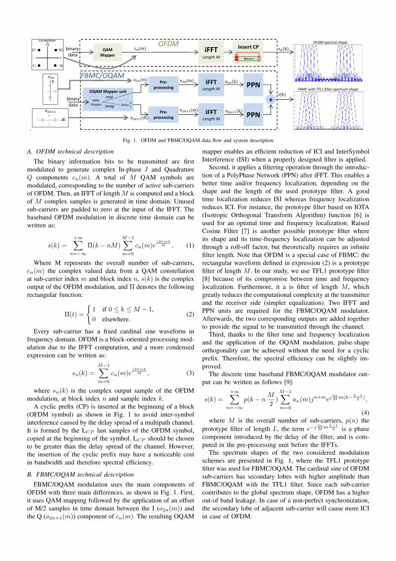
.
s𝑛(k) QAM Mapper
iFFT Length M
Insert CP
c𝑛(m) binary data
OFDM
Pre- processing
iFFT Length M
iFFT Length M
PPN
PPN
+
Pre- processing a2𝑛+1(m)
a2𝑛(m) x2𝑛(m)
x2𝑛+1(m)
u2𝑛(k)
u2𝑛+1(k)
s(k) binary data
FBMC/OQAM
OQAM Mapper unit
QAM Mapper Delay
𝑀
2
real
imag
a2𝑛
a2𝑛+1
OFDM spectral shape
FBMC with TFL1 filter spectrum shape
Block n CP
Fig. 1. OFDM and FBMC/OQAM data flow and system description
A. OFDM technical description
The binary information bits to be transmitted are firstmodulated to generate complex In-phase I and QuadratureQ components cn(m). A total of M QAM symbols aremodulated, corresponding to the number of active sub-carriersof OFDM. Then, an IFFT of length M is computed and a blockof M complex samples is generated in time domain. Unusedsub-carriers are padded to zero at the input of the IFFT. Thebaseband OFDM modulation in discrete time domain can bewritten as:
s(k) =
+∞∑n=−∞
Π(k − nM)
M−1∑m=0
cn(m)ej2πmkM , (1)
Where M represents the overall number of sub-carriers,cn(m) the complex valued data from a QAM constellationat sub-carrier index m and block index n, s(k) is the complexoutput of the OFDM modulation, and Π denotes the followingrectangular function:
Π(t) =
{1 if 0 ≤ k ≤M − 1,0 elsewhere.
(2)
Every sub-carrier has a fixed cardinal sine waveform infrequency domain. OFDM is a block-oriented processing mod-ulation due to the IFFT computation, and a more condensedexpression can be written as:
sn(k) =
M−1∑m=0
cn(m)ej2πmkM , (3)
where sn(k) is the complex output sample of the OFDMmodulation, at block index n and sample index k.
A cyclic prefix (CP) is inserted at the beginning of a block(OFDM symbol) as shown in Fig. 1 to avoid inter-symbolinterference caused by the delay spread of a multipath channel.It is formed by the LCP last samples of the OFDM symbol,copied at the beginning of the symbol. LCP should be chosento be greater than the delay spread of the channel. However,the insertion of the cyclic prefix may have a noticeable costin bandwidth and therefore spectral efficiency.
B. FBMC/OQAM technical description
FBMC/OQAM modulation uses the main components ofOFDM with three main differences, as shown in Fig. 1. First,it uses QAM mapping followed by the application of an offsetof M/2 samples in time domain between the I (a2n(m)) andthe Q (a2n+1(m)) component of cn(m). The resulting OQAM
mapper enables an efficient reduction of ICI and InterSymbolInterference (ISI) when a properly designed filter is applied.
Second, it applies a filtering operation through the introduc-tion of a PolyPhase Network (PPN) after iFFT. This enables abetter time and/or frequency localization, depending on theshape and the length of the used prototype filter. A goodtime localization reduces ISI whereas frequency localizationreduces ICI. For instance, the prototype filter based on IOTA(Isotropic Orthogonal Transform Algorithm) function [6] isused for an optimal time and frequency localization. RaisedCosine Filter [7] is another possible prototype filter whereits shape and its time-frequency localization can be adjustedthrough a roll-off factor, but theoretically requires an infinitefilter length. Note that OFDM is a special case of FBMC: therectangular waveform defined in expression (2) is a prototypefilter of length M . In our study, we use TFL1 prototype filter[8] because of its compromise between time and frequencylocalization. Furthermore, it a is filter of length M , whichgreatly reduces the computational complexity at the transmitterand the receiver side (simpler equalization). Two IFFT andPPN units are required for the FBMC/OQAM modulator.Afterwards, the two corresponding outputs are added togetherto provide the signal to be transmitted through the channel.
Third, thanks to the filter time and frequency localizationand the application of the OQAM modulation, pulse-shapeorthogonality can be achieved without the need for a cyclicprefix. Therefore, the spectral efficiency can be slightly im-proved.
The discrete time baseband FBMC/OQAM modulator out-put can be written as follows [9]:
s(k) =
+∞∑n=−∞
p(k − nM
2)
M−1∑m=0
an(m)jn+mej2πM m(k−L−1
2 ),
(4)where M is the overall number of sub-carriers, p(n) the
prototype filter of length L, the term e−j2πM mL−1
2 is a phasecomponent introduced by the delay of the filter, and is com-puted in the pre-processing unit before the IFFTs.
The spectrum shapes of the two considered modulationschemes are presented in Fig. 1, where the TFL1 prototypefilter was used for FBMC/OQAM. The cardinal sine of OFDMsub-carriers has secondary lobes with higher amplitude thanFBMC/OQAM with the TFL1 filter. Since each sub-carriercontributes to the global spectrum shape, OFDM has a higherout-of band leakage. In case of a non-perfect synchronization,the secondary lobe of adjacent sub-carrier will cause more ICIin case of OFDM.
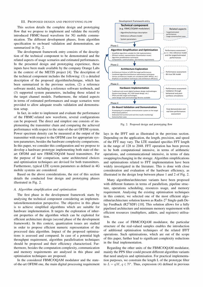
III. PROPOSED DESIGN AND PROTOTYPING FLOW
This section details the complete design and prototypingflow that we propose to implement and validate the recentlyintroduced FBMC-based waveform for 5G mobile commu-nication. The different development phases, from algorithmspecification to on-board validation and demonstration, aresummarized in Fig. 2.
The development framework entry consists of the descrip-tion of the technical component to be demonstrated and therelated aspects of usage scenarios and estimated performances.In the presented design and prototyping experience, theseinputs have been made available by the company Orange Labsin the context of the METIS project [4]. The description ofthe technical component includes the following: (1) a detaileddescription of the proposed algorithm/technique, which hasbeen summarized in the previous section, (2) a referencesoftware model, including a reference software testbench, and(3) supported system parameters, including those related tothe target channel models. Furthermore, the related aspectsin terms of estimated performances and usage scenarios wereprovided to allow adequate results validation and demonstra-tion setup.
In fact, in order to implement and evaluate the performanceof the FBMC-related new waveform, several configurationscan be proposed. The direct and simplest one consists of im-plementing the transmitter chain and comparing the achievedperformance with respect to the state-of-the-art OFDM system.Power spectrum density can be measured at the output of thetransmitter with respect to the OFDM case for appropriate sys-tem parameters, besides the hardware complexity comparisons.In this paper, we consider this configuration and we propose todevelop a hardware prototype implementing both state-of-the-art OFDM and new FBMC/OQAM based transmitters. Forthe purpose of fair comparison, same architectural choicesand optimisation techniques are devised for both transmitters.Furthermore, typical LTE system parameters as defined in 4Gmobile systems are considered.
Based on the above considerations, the rest of this sectiondetails the conducted four design and prototyping phasesillustrated in Fig. 2.
A. Algorithm simplification and optimisation
The first phase in the development framework starts byanalysing the technical component considering an implemen-tation/demonstration perspective. The objective in this phaseis to achieve simplified algorithms which are suitable forhardware implementation. It targets the exploration of inher-ent properties of the algorithm which can be exploited forefficient architecture design (second phase of the developmentframework). In this context, quantization issues are studiedin order to propose efficient numeric representation of theprocessed data algorithm. Impact of the proposed optimisa-tions is assessed and compared. In case of a potential highthroughput requirement, algorithm parallelisation techniquesshould be proposed and their efficiency characterised. Fur-thermore, besides the computation complexity, communicationand memory requirements are analysed in this phase andoptimisation techniques are proposed.
In the considered FBMC/OQAM modulator and the state-of-the-art OFDM one, the main digital processing requirement
Development framework entry
Technical component (e.g. FBMC/OQAM modulator)
- Algorithm/technique description
- Reference software model
- System parameters
Algorithm Simplification and Optimisation
Related aspects - Target/estimated
performances - Usage scenarios/test cases
- Simplified algorithms suitable for HW implementation - Efficient numeric representation (Quantization issues) - Algorithm parallelisation techniques - Computation, communication, and memory requirements
Performance assessment w.r.t. t the reference model
and the target/estimated performances
Phase 1
Architecture Exploration - Architectural choices to fulfill the target performances - Combined algorithm/architecture optimization techniques - Various architecture models are considered (ASIP, MPSoC, etc.) - Emphasis on parallelism techniques and architecture efficiency
- Performance assessment - Bit-true SW model
Phase 2
Hardware Implementation - Traditional and recent digital hardware design methodologies
(System-level design, HLS, ASIP-based design, etc.) - FPGA and ASIC target technologies - Latest design tools and technology libraries available
Phase 3
On-Board Validation and Demonstration - Prototyping of a complete communication system on the target
FPGA-based platform - Dedicated GUI (control and real time results monitoring) - Scenarios/test cases
Final demonstrator and real time performances
assessment
Phase 4
- Performance assessment - Validation through
behavioral and post-synthesis simulations
Fig. 2. Proposed design and prototyping flow
lays in the IFFT unit as illustrated in the previous section.Depending on the application, the length, precision, and speedof the FFT may vary. The LTE standard specifies FFT lengthin the range of 128 to 2048. FFT operation has been provento be both computational intensive, in terms of arithmeticoperations, and communicational intensive, in terms of dataswapping/exchanging in the storage. Algorithm simplificationsand optimisations related to FFT implementation have beenwidely investigated in the literature. This is done with closeconsideration and evaluation of the hardware efficiency, asillustrated in the design loop between phase 1 and 2 of Fig. 2.
Many algorithm/architecture variants have been proposedwith different features in terms of parallelism, pipeline struc-ture, operations scheduling, resources usage, and memoryrequirement. Analysing the existing optimisation techniquesin this context, we selected one of the most efficient algo-rithm/architecture solution known as Radix-22 Single-path De-lay Feedback (R22SDF) [10]. This solution allows for a fullypipelined architecture and minimum memory requirement withefficient resources (multipliers, adders, and registers) utilisa-tion.
In the case of FBMC/OQAM modulator, the particularstructure of the real-valued samples enables the introductionof additional optimisation techniques of the related IFFToperations. Such optimisations, which are out of the scopeof this paper, further lead to significant complexity reductionsin the final implementation.
Regarding the other units of the FBMC/OQAM modulator,mainly the PPN filter could present different algorithm variantsthat need analysis and optimisation. For practical implementa-tion purposes, we constrain the length L of the prototype filterto L = qM , q ∈ N∗. Thus, expression (4) defined in previous
section becomes:
s(k) =
+∞∑n=−∞
p(k − nM
2)
M−1∑m=0
xn(m) ej2πM mk,
xn(m) = an(m)jn+m (−1)qm ejπmM (5)
The other units imply standard low-complexity computationswhere simple architecture optimisations can be done in phase2 of the development flow.
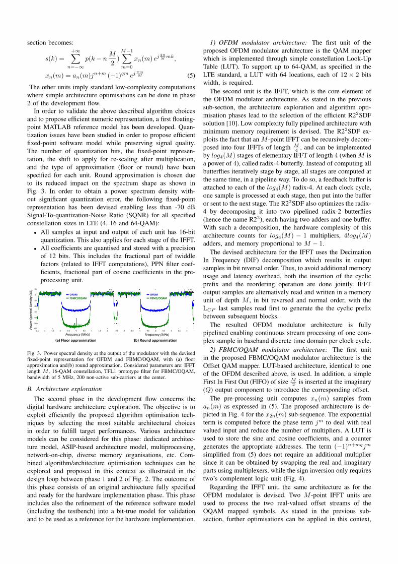
In order to validate the above described algorithm choicesand to propose efficient numeric representation, a first floating-point MATLAB reference model has been developed. Quan-tization issues have been studied in order to propose efficientfixed-point software model while preserving signal quality.The number of quantization bits, the fixed-point represen-tation, the shift to apply for re-scaling after multiplication,and the type of approximation (floor or round) have beenspecified for each unit. Round approximation is chosen dueto its reduced impact on the spectrum shape as shown inFig. 3. In order to obtain a power spectrum density with-out significant quantization error, the following fixed-pointrepresentation has been devised enabling less than -70 dBSignal-To-quantization-Noise Ratio (SQNR) for all specifiedconstellation sizes in LTE (4, 16 and 64-QAM):• All samples at input and output of each unit has 16-bit
quantization. This also applies for each stage of the IFFT.• All coefficients are quantised and stored with a precision
of 12 bits. This includes the fractional part of twiddlefactors (related to IFFT computations), PPN filter coef-ficients, fractional part of cosine coefficients in the pre-processing unit.
Frequency (MHz) Frequency (MHz)
Pow
er S
pec
tra
l Den
sity
(d
B)
(a) Floor approximation (b) Round approximation
OFDM FBMC/OQAM
OFDM FBMC/OQAM
-2.5 -2 -1.5 -1 -0.5 0 0.5 1 1.5 2 -2.5 -2 -1.5 -1 -0.5 0 0.5 1 1.5 2 -60
-50
-40
-30
-20
-10
0
10
Fig. 3. Power spectral density at the output of the modulator with the devisedfixed-point representation for OFDM and FBMC/OQAM, with (a) floorapproximation and(b) round approximation. Considered parameters are: IFFTlength M , 16-QAM constellation, TFL1 prototype filter for FBMC/OQAM,bandwidth of 5 MHz, 200 non-active sub-carriers at the center.
B. Architecture explorationThe second phase in the development flow concerns the
digital hardware architecture exploration. The objective is toexploit efficiently the proposed algorithm optimisation tech-niques by selecting the most suitable architectural choicesin order to fulfill target performances. Various architecturemodels can be considered for this phase: dedicated architec-ture model, ASIP-based architecture model, multiprocessing,network-on-chip, diverse memory organisations, etc. Com-bined algorithm/architecture optimisation techniques can beexplored and proposed in this context as illustrated in thedesign loop between phase 1 and 2 of Fig. 2. The outcome ofthis phase consists of an original architecture fully specifiedand ready for the hardware implementation phase. This phaseincludes also the refinement of the reference software model(including the testbench) into a bit-true model for validationand to be used as a reference for the hardware implementation.
1) OFDM modulator architecture: The first unit of theproposed OFDM modulator architecture is the QAM mapperwhich is implemented through simple constellation Look-UpTable (LUT). To support up to 64-QAM, as specified in theLTE standard, a LUT with 64 locations, each of 12 × 2 bitswidth, is required.
The second unit is the IFFT, which is the core element ofthe OFDM modulator architecture. As stated in the previoussub-section, the architecture exploration and algorithm opti-misation phases lead to the selection of the efficient R22SDFsolution [10]. Low complexity fully pipelined architecture withminimum memory requirement is devised. The R22SDF ex-ploits the fact that an M -point IFFT can be recursively decom-posed into four IFFTs of length M
4 , and can be implementedby log4(M) stages of elementary IFFT of length 4 (when M isa power of 4), called radix-4 butterfly. Instead of computing allbutterflies iteratively stage by stage, all stages are computed atthe same time, in a pipeline way. To do so, a feedback buffer isattached to each of the log4(M) radix-4. At each clock cycle,one sample is processed at each stage, then put into the bufferor sent to the next stage. The R22SDF also optimizes the radix-4 by decomposing it into two pipelined radix-2 butterflies(hence the name R22), each having two adders and one buffer.With such a decomposition, the hardware complexity of thisarchitecture counts for log4(M) − 1 multipliers, 4log4(M)adders, and memory proportional to M − 1.
The devised architecture for the IFFT uses the DecimationIn Frequency (DIF) decomposition which results in outputsamples in bit reversal order. Thus, to avoid additional memoryusage and latency overhead, both the insertion of the cyclicprefix and the reordering operation are done jointly. IFFToutput samples are alternatively read and written in a memoryunit of depth M , in bit reversed and normal order, with theLCP last samples read first to generate the the cyclic prefixbetween subsequent blocks.
The resulted OFDM modulator architecture is fullypipelined enabling continuous stream processing of one com-plex sample in baseband discrete time domain per clock cycle.
2) FBMC/OQAM modulator architecture: The first unitin the proposed FBMC/OQAM modulator architecture is theOffset QAM mapper. LUT-based architecture, identical to oneof the OFDM described above, is used. In addition, a simpleFirst In First Out (FIFO) of size M
2 is inserted at the imaginary(Q) output component to introduce the corresponding offset.
The pre-processing unit computes xn(m) samples froman(m) as expressed in (5). The proposed architecture is de-picted in Fig. 4 for the x2n(m) sub-sequence. The exponentialterm is computed before the phase term jm to deal with realvalued input and reduce the number of multipliers. A LUT isused to store the sine and cosine coefficients, and a countergenerates the appropriate addresses. The term (−1)n+mqjm
simplified from (5) does not require an additional multipliersince it can be obtained by swapping the real and imaginaryparts using multiplexers, while the sign inversion only requirestwo’s complement logic unit (Fig. 4).
Regarding the IFFT unit, the same architecture as for theOFDM modulator is devised. Two M -point IFFT units areused to process the two real-valued offset streams of theOQAM mapped symbols. As stated in the previous sub-section, further optimisations can be applied in this context,
a2𝑛(m)
pipeline register
X
LUT D𝑒𝑝𝑡ℎ 𝑀
2
X
sin(𝜋𝑚𝑀 )
Counter Modulo 2M
0 1
0 1
0 1
0 1
XOR
Address mapping
𝑎𝑑𝑑𝑟𝑐𝑜𝑠
𝑎𝑑𝑑𝑟𝑠𝑖𝑛
cnt(1)
𝑗𝑚
cnt(0)
cnt
L
cnt(L-1)
(−1)𝑛+𝑚
(if q odd)
x
x
-1 𝑟𝑒𝑎𝑙(𝑥2𝑛(𝑚))
𝑖𝑚𝑎𝑔(𝑥2𝑛(𝑚)) -1
x
cos(𝜋𝑚𝑀 )
-1
1 0
Pre-processing
Fig. 4. Proposed architecture for the pre-processing unit
X
LUT Depth M
(x2)
Counter Modulo M
𝑢2𝑛 𝑘
FIFO Depth M
LUT Depth M
X
FIFO Depth M
(x2)
LUT Depth M
X (x2)
Cascaded adder
+ +
Counter Modulo M
PolyPhase Network 1
𝑠 𝑘 Counter Modulo M
X (x2)
𝑢2𝑛+1 𝑘 X (x2)
X (x2)
𝑢2𝑛−2 𝑘 𝑢2𝑛−4 𝑘
FIFO Depth M
FIFO Depth M
Cascaded adder
+ +
PolyPhase Network 2
+ R E S C A L E
𝑢2𝑛−1 𝑘 𝑢2𝑛−3 𝑘
Pipeline register
Fig. 5. Proposed PPN architecture for a filter length L = 3M with sharedcoefficient memories
however they are out of the scope of this paper. Furthermore,reorder units are used as in the OFDM modulator, exceptthat cyclic prefix insertion is removed in the FBMC/OQAMmodulator.
Hardware resource Quantity
RAM of depth M2
for ping-pong FIFO implementationa 4(q − 1)LUT of depth M qReal multipliers 4qReal adders 4q − 2a Note that for a one tap PPN (L = M ), the FIFOs are not needed
TABLE IPPN ARCHITECTURE COMPLEXITY FOR A FILTER OF LENGTH L = qM
The last unit of the FBMC/OQAM modulator is the PPNfilter. Fig. 5 illustrates the devised architecture for a filterlength L = 3M . The proposed architecture is derived from[11] with adaptation to the OQAM components structure.Filter coefficients are stored in shared memories between thetwo PPN units. Table I summarizes the PPN architecturecomplexity considering a filter of length L = qM . To optimizethe number of pipeline registers, the cascaded adders shouldbe mapped in a tree structure (applicable when q > 3).
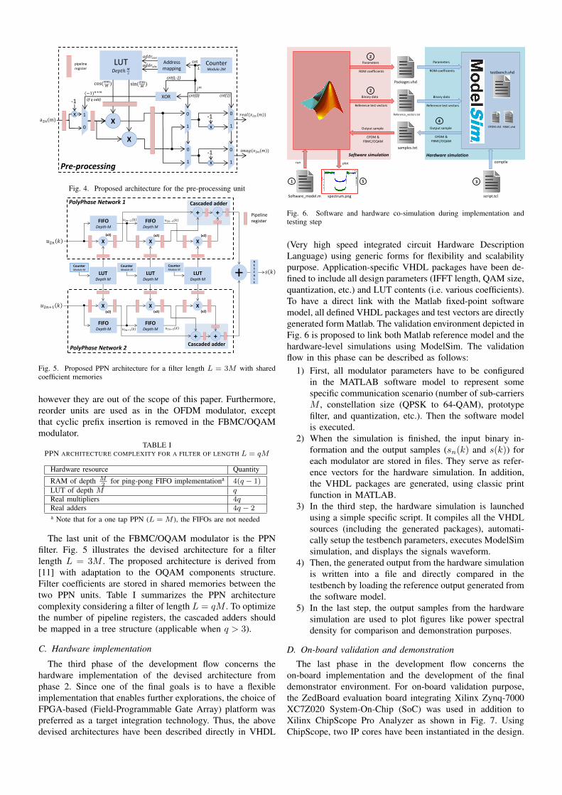
C. Hardware implementation
The third phase of the development flow concerns thehardware implementation of the devised architecture fromphase 2. Since one of the final goals is to have a flexibleimplementation that enables further explorations, the choice ofFPGA-based (Field-Programmable Gate Array) platform waspreferred as a target integration technology. Thus, the abovedevised architectures have been described directly in VHDL
Packages.vhd
Reference_vectors.txt
samples.txt
script.tcl
Parameters ROM coefficients
Binary data Reference test vectors
Output sample
OFDM & FBMC/OQAM
testbench.vhd
OFDM.vhd
compile
Software_model.m
Software simulation
run plot
spectrum.png
Parameters ROM coefficients
Binary data Reference test vectors
Hardware simulation
Output sample
OFDM & FBMC/OQAM
1
2
2
3
4
5
FBMC.vhd
Fig. 6. Software and hardware co-simulation during implementation andtesting step
(Very high speed integrated circuit Hardware DescriptionLanguage) using generic forms for flexibility and scalabilitypurpose. Application-specific VHDL packages have been de-fined to include all design parameters (IFFT length, QAM size,quantization, etc.) and LUT contents (i.e. various coefficients).To have a direct link with the Matlab fixed-point softwaremodel, all defined VHDL packages and test vectors are directlygenerated form Matlab. The validation environment depicted inFig. 6 is proposed to link both Matlab reference model and thehardware-level simulations using ModelSim. The validationflow in this phase can be described as follows:
1) First, all modulator parameters have to be configuredin the MATLAB software model to represent somespecific communication scenario (number of sub-carriersM , constellation size (QPSK to 64-QAM), prototypefilter, and quantization, etc.). Then the software modelis executed.
2) When the simulation is finished, the input binary in-formation and the output samples (sn(k) and s(k)) foreach modulator are stored in files. They serve as refer-ence vectors for the hardware simulation. In addition,the VHDL packages are generated, using classic printfunction in MATLAB.
3) In the third step, the hardware simulation is launchedusing a simple specific script. It compiles all the VHDLsources (including the generated packages), automati-cally setup the testbench parameters, executes ModelSimsimulation, and displays the signals waveform.
4) Then, the generated output from the hardware simulationis written into a file and directly compared in thetestbench by loading the reference output generated fromthe software model.
5) In the last step, the output samples from the hardwaresimulation are used to plot figures like power spectraldensity for comparison and demonstration purposes.
D. On-board validation and demonstration
The last phase in the development flow concerns theon-board implementation and the development of the finaldemonstrator environment. For on-board validation purpose,the ZedBoard evaluation board integrating Xilinx Zynq-7000XC7Z020 System-On-Chip (SoC) was used in addition toXilinx ChipScope Pro Analyzer as shown in Fig. 7. UsingChipScope, two IP cores have been instantiated in the design.
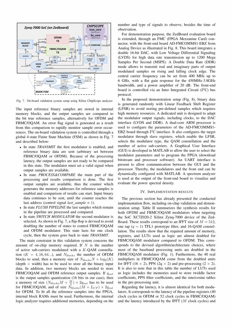
FBMC/OQAM TX
OFDM TX
MEMORY BLOCK
MAIN FSM
COUNTER
COUNTER
addr
addr
error_flag
Ila_core (Xilinx IP core)
Icon_core (Xilinx IP core)
CHIPSCOPE Zynq-7000 SoC (on Zedboard)
COMPARE
PROCESS & COMPARE
SWITCH MODULATOR
last_sample = 1
last_compare = 1
valid = 1
NOT
Flip- Flop
en_FBMC
en_OFDM
en_data
valid_OFDM
valid_FBMC
valid
select
select
1 0
0 1
switch
MEMORY BLOCK
MEMORY BLOCK
s𝑛(k)
s(k)
ref_OFDM ref_FBMC
en_compare
0 1
1 0
last_compare
last_sample
en_data = 1 en_compare = 1 switch = 0
en_data = 1 en_compare = 0 switch = 0
en_data = 0 en_compare = 1 switch = 0
en_data = 0 en_compare = 0 switch = 1
MAIN FSM
FLUSH PIPELINE
q𝑜𝑢𝑡
TRANSMIT
Binary data
Fig. 7. On-board validation system setup using Xilinx ChipScope analyzer
The input reference binary samples are stored in internalmemory blocks, and the output samples are compared tothe bit true reference samples, alternatively for OFDM andFBMC/OQAM. An error flag signal is generated as a resultfrom this comparison to rapidly monitor sample error occur-rences. The on-board validation system is controlled through aglobal 4-state Finite State Machine (FSM) as shown in Fig. 7and described below:• In state TRANSMIT the first modulator is enabled, and
reference binary data are sent (arbitrary set betweenFBMC/OQAM or OFDM). Because of the processinglatency, the output samples are not ready to be comparedin this state. The modulator must set a valid signal whenoutput samples are available.
• In state PROCESS&COMPARE the main part of theprocessing and results comparison is done. The firstoutput samples are available, thus the counter whichgenerates the memory addresses for reference samples isenabled and comparison of results can start. Input binarydata continues to be sent, until the counter reaches thelast address (control signal last sample = 1).
• In state FLUSH PIPELINE the last samples which remainin the pipeline are processed and compared.
• In state SWITCH MODULATOR the second modulator isselected. As shown in Fig. 7, a flip-flop is devised to avoiddoubling the number of states to control FBMC/OQAMand OFDM modulator. This state lasts for one clockcycle, then the system goes back to state TRANSMIT.
The main constraint in this validation system concerns theamount of on-chip memory required. If N is the numberof active sub-carriers modulated with a K-QAM constella-tion (K = 4, 16, 64...), and Nblocks the number of OFDMblocks to send, then a memory size of NblocksN × log2(K)(depth × width) has to be used to store all the binary inputdata. In addition, two memory blocks are needed to storeFBMC/OQAM and OFDM reference output samples. If qoutis the output samples quantization (16 bits in our case), thena memory of size (NblocksM + M
2 ) × 2qout has to be usedfor FBMC/OQAM, and of size Nblocks(M + LCP ) × 2qoutfor OFDM. To fit all the reference samples into the FPGA,internal block RAMs must be used. Furthermore, the internallogic analyzer requires additional memories, depending on the
number and type of signals to observe, besides the time ofobservation.
For demonstration purpose, the ZedBoard evaluation boardis extended, through an FMC (FPGA Mezzanine Card) con-nector, with the front-end board AD-FMCOMMS1-EBZ fromAnalog Device as illustrated in Fig. 8. This board integrates adouble 16-bit DAC, with Low Voltage Differential Signaling(LVDS) for high data rate transmission up to 1200 MegaSamples Per Second (MSPS). A Double Data Rate (DDR)mode allows to transmit real and imaginary parts of outputmodulated samples on rising and falling clock edge. Thecentral carrier frequency can be set from 400 MHz up to6 GHz, with a flat gain response for the 450MHz-3.8GHzbandwidth, and a power amplifier of 20 dB. The front-endboard is controlled via an Inter Integrated Circuit (I2C) busprotocol.
In the proposed demonstration setup (Fig. 8), binary datais generated randomly with Linear Feedback Shift Register(LFSR) to avoid storing pre-defined samples which requireshigh memory resources. A dedicated unit is designed to adaptthe modulator output signals, including clocks, to the DACinterface (LVDS and DDR). A dual-core ARM processor isused to configure the parameters of the AD-FMCOMMS1-EBZ board through I2C interface. It also configures the targetmodulator through slave registers, which enable the LFSR,selects the modulator type, the QAM constellation and thenumber of active sub-carriers. A Graphical User Interface(GUI) is developed in MATLAB to allow the user to select themodulator parameters and to program the FPGA (downloadbitstream and processor software). An UART interface ispresent to allow communication between the GUI and theprocessor. Thereby, the modulators and the front end can bedynamically configured with MATLAB. A spectrum analyzeris used at the output of the front-end board to visualize andevaluate the power spectral density.
IV. IMPLEMENTATION RESULTS
The previous section has already presented the conductedimplementation flow, including on-chip validation and demon-stration setup. Table II summarizes the synthesis results forboth OFDM and FBMC/OQAM modulators when targetingthe SoC XC7Z020-2 Xilinx Zynq-7000 device of the Zed-Board. These results correspond to an IFFT size of M = 512,one tap (q = 1) TFL1 prototype filter, and 16-QAM constel-lation. The results show that the required amount of memory,registers, and LUTs used as logic are almost doubled forFBMC/OQAM modulator compared to OFDM. This corre-sponds to the devised algorithm/architecture choices, wheremost of the baseband processing units are doubled in theFBMC/OQAM modulator (Fig. 1). Furthermore, the 40 realmultipliers in FBMC/OQAM come from the doubled unitsfor IFFT (16 × 2), PPN (2q × 2) and pre-processing (2 × 2).It is also to note that in this table the number of LUTs usedas logic includes the memories used to store twiddle factorcoefficients, PPN filter coefficients, and the sine/cosine tablesin the pre-processing unit.
Regarding the latency, it is almost identical for both modu-lators. It corresponds to the latency of the pipeline registers (40clock cycles in OFDM or 52 clock cycles in FBMC/OQAM)and the latency introduced by the IFFT (M clock cycles) and
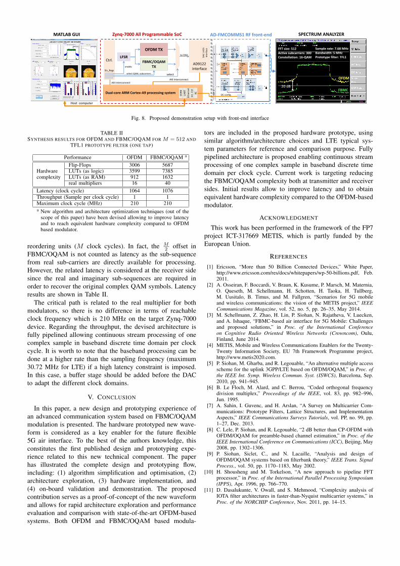
Zynq-7000 All Programmable SoC
to DAC
I2C config.
Host computer
Dual-core ARM Cortex-A9 processing system
LFSR Ctrl.
Slv_Regs
IIC
Int.
Ctr
l
Eth
ern
et
UA
RT
DD
RX
AD9122 interface
DA
C L
VD
S In
terf
ace
AXI Interconnect AXI Interconnect
AD-FMCOMMS1 RF front-end MATLAB GUI
OFDM TX
FBMC/OQAM TX
FFT size: 512 Active subcarriers: 300 Constellation: 16-QAM
Sample rate: 7.68 MHz Bandwidth: 5 MHz Prototype filter: TFL1
FBMC
OFDM
20 dB
SPECTRUM ANALYZER
select select QAM, subcarriers…
enable
Fig. 8. Proposed demonstration setup with front-end interface
TABLE IISYNTHESIS RESULTS FOR OFDM AND FBMC/OQAM FOR M = 512 AND
TFL1 PROTOTYPE FILTER (ONE TAP)
Performance OFDM FBMC/OQAM a
Flip-Flops 3006 5687Hardware LUTs (as logic) 3599 7385complexity LUTs (as RAM) 912 1632
real multipliers 16 40Latency (clock cycle) 1064 1076Throughput (Sample per clock cycle) 1 1Maximum clock cycle (MHz) 210 210a New algorithm and architecture optimization techniques (out of the
scope of this paper) have been devised allowing to improve latencyand to reach equivalent hardware complexity compared to OFDMbased modulator.
reordering units (M clock cycles). In fact, the M2 offset in
FBMC/OQAM is not counted as latency as the sub-sequencefrom real sub-carriers are directly available for processing.However, the related latency is considered at the receiver sidesince the real and imaginary sub-sequences are required inorder to recover the original complex QAM symbols. Latencyresults are shown in Table II.
The critical path is related to the real multiplier for bothmodulators, so there is no difference in terms of reachableclock frequency which is 210 MHz on the target Zynq-7000device. Regarding the throughput, the devised architecture isfully pipelined allowing continuous stream processing of onecomplex sample in baseband discrete time domain per clockcycle. It is worth to note that the baseband processing can bedone at a higher rate than the sampling frequency (maximum30.72 MHz for LTE) if a high latency constraint is imposed.In this case, a buffer stage should be added before the DACto adapt the different clock domains.
V. CONCLUSION
In this paper, a new design and prototyping experience ofan advanced communication system based on FBMC/OQAMmodulation is presented. The hardware prototyped new wave-form is considered as a key enabler for the future flexible5G air interface. To the best of the authors knowledge, thisconstitutes the first published design and prototyping expe-rience related to this new technical component. The paperhas illustrated the complete design and prototyping flow,including: (1) algorithm simplification and optimisation, (2)architecture exploration, (3) hardware implementation, and(4) on-board validation and demonstration. The proposedcontribution serves as a proof-of-concept of the new waveformand allows for rapid architecture exploration and performanceevaluation and comparison with state-of-the-art OFDM-basedsystems. Both OFDM and FBMC/OQAM based modula-
tors are included in the proposed hardware prototype, usingsimilar algorithm/architecture choices and LTE typical sys-tem parameters for reference and comparison purpose. Fullypipelined architecture is proposed enabling continuous streamprocessing of one complex sample in baseband discrete timedomain per clock cycle. Current work is targeting reducingthe FBMC/OQAM complexity both at transmitter and receiversides. Initial results allow to improve latency and to obtainequivalent hardware complexity compared to the OFDM-basedmodulator.
ACKNOWLEDGMENT
This work has been performed in the framework of the FP7project ICT-317669 METIS, which is partly funded by theEuropean Union.
REFERENCES
[1] Ericsson, “More than 50 Billion Connected Devices,” White Paper,http://www.ericsson.com/res/docs/whitepapers/wp-50-billions.pdf, Feb.2011.
[2] A. Osseiran, F. Boccardi, V. Braun, K. Kusume, P. Marsch, M. Maternia,O. Queseth, M. Schellmann, H. Schotten, H. Taoka, H. Tullberg,M. Uusitalo, B. Timus, and M. Fallgren, “Scenarios for 5G mobileand wireless communications: the vision of the METIS project,” IEEECommunications Magazine, vol. 52, no. 5, pp. 26–35, May 2014.
[3] M. Schellmann, Z. Zhao, H. Lin, P. Siohan, N. Rajatheva, V. Luecken,and A. Ishaque, “FBMC-based air interface for 5G Mobile: Challengesand proposed solutions,” in Proc. of the International Conferenceon Cognitive Radio Oriented Wireless Networks (Crowncom), Oulu,Finland, June 2014.
[4] METIS, Mobile and Wireless Communications Enablers for the Twenty-Twenty Information Society, EU 7th Framework Programme project,http://www.metis2020.com.
[5] P. Siohan, M. Gharba, and R. Legouable, “An alternative multiple accessscheme for the uplink 3GPP/LTE based on OFDM/OQAM,” in Proc. ofthe IEEE Int. Symp. Wireless Commun. Syst. (ISWCS), Barcelona, Sep.2010, pp. 941–945.
[6] B. Le Floch, M. Alard, and C. Berrou, “Coded orthogonal frequencydivision multiplex,” Proceedings of the IEEE, vol. 83, pp. 982–996,Jun. 1995.
[7] A. Sahin, I. Guvenc, and H. Arslan, “A Survey on Multicarrier Com-munications: Prototype Filters, Lattice Structures, and ImplementationAspects,” IEEE Communications Surveys Tutorials, vol. PP, no. 99, pp.1–27, Dec. 2013.
[8] C. Lele, P. Siohan, and R. Legouable, “2 dB better than CP-OFDM withOFDM/OQAM for preamble-based channel estimation,” in Proc. of theIEEE International Conference on Communications (ICC), Beijing, May2008, pp. 1302–1306.
[9] P. Siohan, Siclet, C., and N. Lacaille, “Analysis and design ofOFDM/OQAM systems based on filterbank theory,” IEEE Trans. SignalProcess., vol. 50, pp. 1170–1183, May 2002.
[10] H. Shousheng and M. Torkelson, “A new approach to pipeline FFTprocessor,” in Proc. of the International Parallel Processing Symposium(IPPS), Apr. 1996, pp. 766–770.
[11] D. Dasalukunte, V. Owall, and S. Mehmood, “Complexity analysis ofIOTA filter architectures in faster-than-Nyquist multicarrier systems,” inProc. of the NORCHIP Conference, Nov. 2011, pp. 14–15.