Embed Size (px)
Citation preview

Hardware Modeling using Verilog Prof. Indranil Sengupta
Department of Computer Science and Engineering Indian Institute of Technology, Kharagpur
Lecture - 10
Verilog Modeling Examples
So, if you recall the topics that we have discussed during our last few lectures, we have
talked about the various constructs of the Verilog language. We had looked at some of the
fundamental constructs, the operators, how we can frame the expressions for evaluation
and some of the operations we have defined for assignment. For example, using the assign
statement, there are a few more, which will be discussing in the due course of the lectures.
But what we are trying to deal with in the present lecture is, we shall take an example. And
with the help of an example we shall try to illustrate a few points and concepts which are
considered to be good design practice when someone is going about designing a digital
system, using a hardware description language.
So, the topic of our lecture is Verilog Modeling Examples. Now actually what we trying
to do here let me try to explain this first. You have seen that when we model some system
using Verilog, broadly there are two fundamental ways of doing it. So, we call it
Behavioral and Structural modeling.
(Refer Slide Time: 01:45)

You can do either using behavioral or using structural. Now in the example that I shall be
giving in this lecture, we shall be just elaborating on this further.
Now, just to tell you about when we talk about behavioral modeling, what we are actually
doing. We are actually saying that how a system is working, we are not telling or talking
about how it is actually constructed or is to be constructed. We are saying that for example,
I have an adder, this some output should be a XOR b XOR c, they carry output should be
ab OR bc OR ca. So, I am not telling that whether you will be using AND gate, OR gate,
NOT gate, or NAND gate, or XOR gate, what or how you will be interconnecting them.
So, if I say just the behavior, either in the form of this expression or in the form of a truth
table let us say that is a so called behavioral expression which is much easier to do. So,
when you are designer, when you have something in your head, in your mind, you are
trying to design something. So, the first thing that you can write or start with is a behavioral
description of your model, or your thought process, what you are thinking about. Now
once you have thought about the behavior, now you can think about how you can
implement it, ok.
Let us say, let us take that same example of a full adder. So, once you have thought about
what is the functionality of a full adder. Now you think about how you want to implement
it. Now you may see that, well, I want to implement it using a technology, where you have
only NAND gates. So, let us not use AND, OR, or NOT operation. So, all the AND, OR,
NOT, whatever is there we will be translating them using Demorgan’s Law, using NAND
operations only and we will be implementing it using NAND; so just in this diagram.
So, as I had said behavioral description is often the starting point, because it is easier to
write a Verilog module in the behavioral model, but structural description, this is more
with respect to hardware implementation. Like here, I can say that well to implement the
carry output of the full adder, let us say to implement carry, I need a, I will say that I will
need four NAND gates, let us say. And I will also tell how the NAND gates are
interconnected. I will say that well you interconnect the NAND gates like this, there will
be three 2-input NAND gates and one 3-input NAND gate, this will be ab, bc and ca and
this will be your final carry output (cy).
So, this is; what is your structural representation, you specify some modules and you also
tell how they are interconnected. Now obviously, this is much more detailed. So, when

you are thinking of the behavior, you have not yet thought about these gates and how they
are interconnected, ok. So, there will be a process that you will have to go through that
from behavioral to structural, you will have to make a translation, right. So, the normal
designed process is that we start with a behavioral description, now in our behavioral
description our total description may consist of one or may be multiple modules.
Let say one, we systematically try to convert them into structural descriptions, that can be
several steps. I shall take one example and I will show you that how you can use several
steps in the translation, and how you can carry out some kind of a hierarchical design
process in order to achieve it. At the end of which you will be having a number of modules,
all of which are specified in a structural description. So, you have a total design which is
a structural description of a system you want to built.
So, from behavioral to structural, this is normally the step which many people follow, ok.
So, we shall be taking the example of a 16-to-1 multiplexer and illustrate some of the
(Refer Slide Time: 06:58)
points I have just discussed with respect to this. 16 to 1 multiplexer, you know what a 16
to 1 multiplexer is.

(Refer Slide Time: 07:19)
So, a multiplexer has a number of input lines, a single output line and a number of select
lines. So, when I say a 16 to 1 multiplexer. So, there will be 16 input lines, there will be
one output line, and to select one of the input lines there will be four select lines.
So, the rule is, number of select lines is given by log to the base 2 of the number of input
lines. Here input lines is 16. So, log to the base of 16 will be 4, right. So, we are trying to
design such a multiplexer. So, to start with, we shall be giving the behavior. So, I am just
showing you in this list that how we shall be proceeding with our design. So, in the first
step, we shall be using pure behavioral modeling, which we shall see will be rather simple,
specifying the behavior of a 16 to 1 multiplexer is very easy.
Then we shall be implementing the 16 to 1 multiplexer using several 4 to 1 multiplexers.
So, we will be using structural description of this 16 to 1 mux, using 4 to 1 multiplexers,
but the 4 to 1 multiplexers will still specify, using behavioral model. Then we shall be
implementing the 4 to 1 mux using 2 to 1 mux and we will be using still behavioral model
of 2 to 1 mux. And finally, we will be specifying these 2 to 1 mux, also in the structural
get level form. So, that we have a complete hierarchical structural description. So, let us
see. So, as we proceed with this example, these steps will be clear. So, we start with pure
behavioral modeling.
(Refer Slide Time: 09:43)
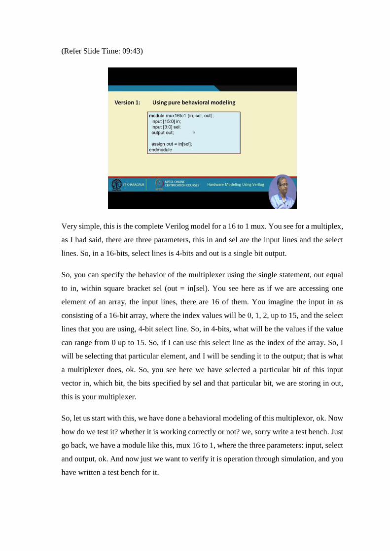
Very simple, this is the complete Verilog model for a 16 to 1 mux. You see for a multiplex,
as I had said, there are three parameters, this in and sel are the input lines and the select
lines. So, in a 16-bits, select lines is 4-bits and out is a single bit output.
So, you can specify the behavior of the multiplexer using the single statement, out equal
to in, within square bracket sel (out = in[sel). You see here as if we are accessing one
element of an array, the input lines, there are 16 of them. You imagine the input in as
consisting of a 16-bit array, where the index values will be 0, 1, 2, up to 15, and the select
lines that you are using, 4-bit select line. So, in 4-bits, what will be the values if the value
can range from 0 up to 15. So, if I can use this select line as the index of the array. So, I
will be selecting that particular element, and I will be sending it to the output; that is what
a multiplexer does, ok. So, you see here we have selected a particular bit of this input
vector in, which bit, the bits specified by sel and that particular bit, we are storing in out,
this is your multiplexer.
So, let us start with this, we have done a behavioral modeling of this multiplexor, ok. Now
how do we test it? whether it is working correctly or not? we, sorry write a test bench. Just
go back, we have a module like this, mux 16 to 1, where the three parameters: input, select
and output, ok. And now just we want to verify it is operation through simulation, and you
have written a test bench for it.
(Refer Slide Time: 12:03)
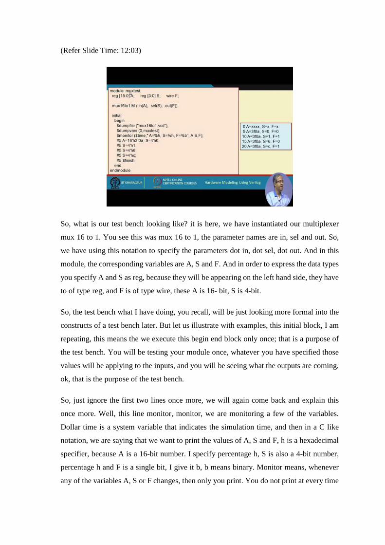
So, what is our test bench looking like? it is here, we have instantiated our multiplexer
mux 16 to 1. You see this was mux 16 to 1, the parameter names are in, sel and out. So,
we have using this notation to specify the parameters dot in, dot sel, dot out. And in this
module, the corresponding variables are A, S and F. And in order to express the data types
you specify A and S as reg, because they will be appearing on the left hand side, they have
to of type reg, and F is of type wire, these A is 16- bit, S is 4-bit.
So, the test bench what I have doing, you recall, will be just looking more formal into the
constructs of a test bench later. But let us illustrate with examples, this initial block, I am
repeating, this means the we execute this begin end block only once; that is a purpose of
the test bench. You will be testing your module once, whatever you have specified those
values will be applying to the inputs, and you will be seeing what the outputs are coming,
ok, that is the purpose of the test bench.
So, just ignore the first two lines once more, we will again come back and explain this
once more. Well, this line monitor, monitor, we are monitoring a few of the variables.
Dollar time is a system variable that indicates the simulation time, and then in a C like
notation, we are saying that we want to print the values of A, S and F, h is a hexadecimal
specifier, because A is a 16-bit number. I specify percentage h, S is also a 4-bit number,
percentage h and F is a single bit, I give it b, b means binary. Monitor means, whenever
any of the variables A, S or F changes, then only you print. You do not print at every time
1 2 3 4, do not continuously go on printing. So, whenever there is a change, then only you
print; that is the purpose of this monitor statement.
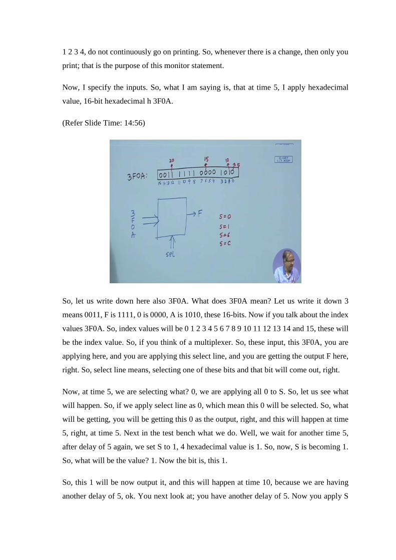
Now, I specify the inputs. So, what I am saying is, that at time 5, I apply hexadecimal
value, 16-bit hexadecimal h 3F0A.
(Refer Slide Time: 14:56)
So, let us write down here also 3F0A. What does 3F0A mean? Let us write it down 3
means 0011, F is 1111, 0 is 0000, A is 1010, these 16-bits. Now if you talk about the index
values 3F0A. So, index values will be 0 1 2 3 4 5 6 7 8 9 10 11 12 13 14 and 15, these will
be the index value. So, if you think of a multiplexer. So, these input, this 3F0A, you are
applying here, and you are applying this select line, and you are getting the output F here,
right. So, select line means, selecting one of these bits and that bit will come out, right.
Now, at time 5, we are selecting what? 0, we are applying all 0 to S. So, let us see what
will happen. So, if we apply select line as 0, which mean this 0 will be selected. So, what
will be getting, you will be getting this 0 as the output, right, and this will happen at time
5, right, at time 5. Next in the test bench what we do. Well, we wait for another time 5,
after delay of 5 again, we set S to 1, 4 hexadecimal value is 1. So, now, S is becoming 1.
So, what will be the value? 1. Now the bit is, this 1.
So, this 1 will be now output it, and this will happen at time 10, because we are having
another delay of 5, ok. You next look at; you have another delay of 5. Now you apply S
equal to 6. So, what is your 6? S is 6, 6 is here. So, this is 0. So, you will be getting a, this
value 0. Now this will happen at time 15 and the last one, you apply S equal to C, C means
12, 1100, right. In hexadecimal S equal to C, C means 12. 12 means, you, here this is 1,
this will happen at time 20, right. And at the end you finish after another time 5, you finish
this simulation.
So, I means if I create this two files and I told you earlier that you can use any of the
simulators to simulate these, and I had suggested to use the Iverilog one, which is very
easy and just freely available. So, here in the examples that I am showing, I have used
Iverilog and GTK wave, to show you the simulation outputs, ok. So, if I just simulate it
using Iverilog. So, I get an output as is shown in the window here, this blue box, see exactly
what I have shown here, this same thing is happening. See at time 5, 0 is coming, at time
10, 1 is coming, at time 15, 0 is coming, at time 20, 1 is coming. You see, the first value
that is printed in the monitor is time, at value of 5 output is F0, 10 output is 1, 15 output is
0, 20 output is 1.
So, I have also printed the values of A and S for your reference, A and also S. Now initially
at time 0, when this simulation starts; so A is not initialized, S is not initialized, F is not
initialized. So, all of them are showing x right, ok. So, you see just from the behavioral
specification, you can do a simulation, and you can get the simulation result like this. Now
the first two lines in the initial statement, I am repeating this. I have mentioned this earlier
also. See these variations with time, this information, you can also dump into a file VCD,
ok. So, here I am giving a name mux 16 to 1 VCD, value change dump file, they will all
be dumped in the file, and I can specify which variables I want to dump.
Well, 0 comma followed by the name of this module means, that all the variables in this
module and all the variables which are instantiated inside those modules, everything will
be dumped. Ok, we shall see what are the other options later in dumpvars, but here we are
dumping all the variables. Now you can ask that well, I can see all the simulation output
like this, why do I need to use this dump file, and dumpvars? the thing is that, well seeing
the simulation output in a tabular form or a just on the screen is not good enough in the
form of a text, well means often for digital circuits, we want to look at the timing diagrams,
how the values are changing at what times and so on.
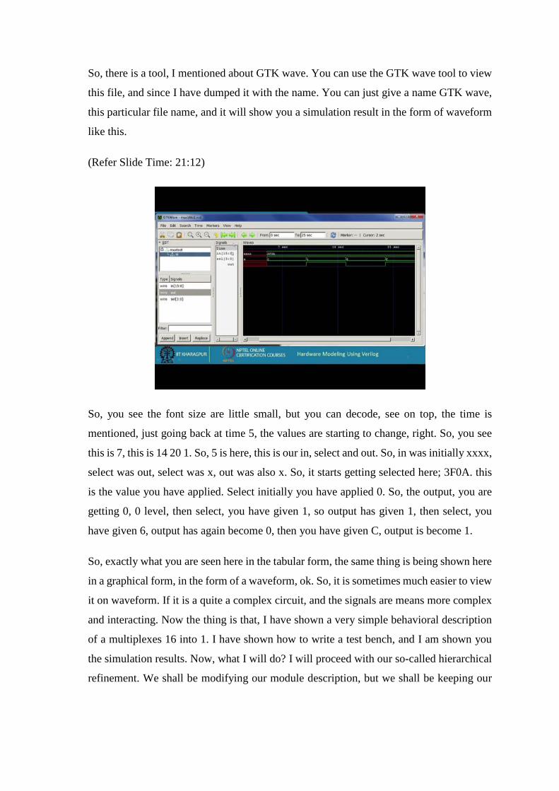
So, there is a tool, I mentioned about GTK wave. You can use the GTK wave tool to view
this file, and since I have dumped it with the name. You can just give a name GTK wave,
this particular file name, and it will show you a simulation result in the form of waveform
like this.
(Refer Slide Time: 21:12)
So, you see the font size are little small, but you can decode, see on top, the time is
mentioned, just going back at time 5, the values are starting to change, right. So, you see
this is 7, this is 14 20 1. So, 5 is here, this is our in, select and out. So, in was initially xxxx,
select was out, select was x, out was also x. So, it starts getting selected here; 3F0A. this
is the value you have applied. Select initially you have applied 0. So, the output, you are
getting 0, 0 level, then select, you have given 1, so output has given 1, then select, you
have given 6, output has again become 0, then you have given C, output is become 1.
So, exactly what you are seen here in the tabular form, the same thing is being shown here
in a graphical form, in the form of a waveform, ok. So, it is sometimes much easier to view
it on waveform. If it is a quite a complex circuit, and the signals are means more complex
and interacting. Now the thing is that, I have shown a very simple behavioral description
of a multiplexes 16 into 1. I have shown how to write a test bench, and I am shown you
the simulation results. Now, what I will do? I will proceed with our so-called hierarchical
refinement. We shall be modifying our module description, but we shall be keeping our
test bench the same. We shall not be touching our test bench. We shall be making
modifications.
We shall be again running the same test bench, and verify whether the simulation results
that you are getting is exactly the same as what we got here. That should be so, because it
should, the result should confirm to a 16 to 1 mux only, this we should verify at every step,
fine.
(Refer Slide Time: 23:28)
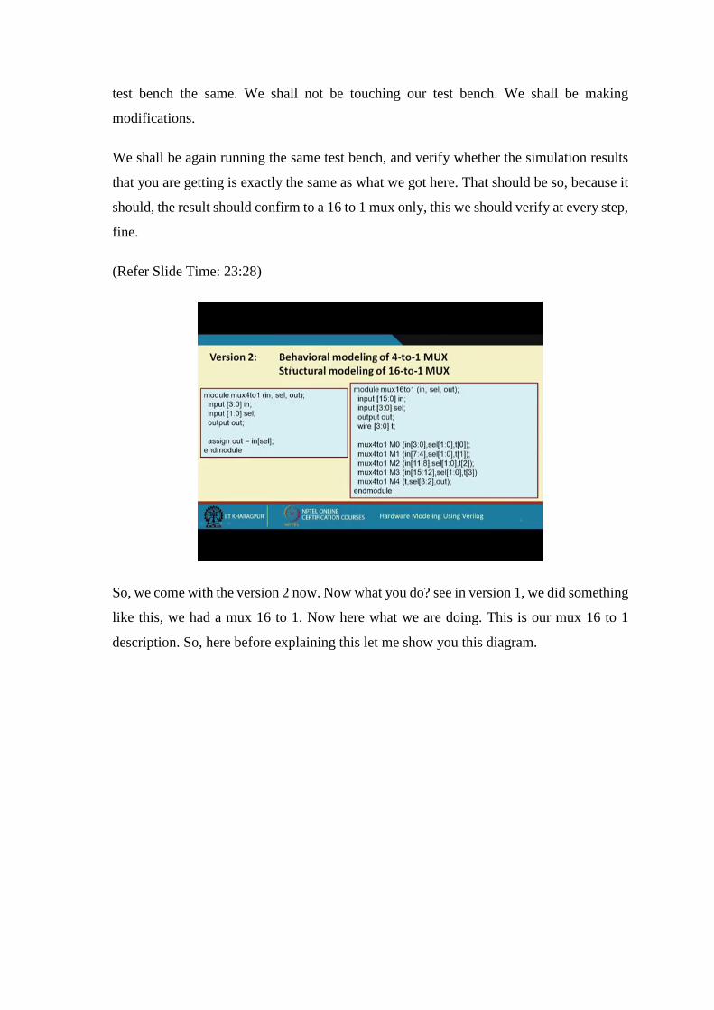
So, we come with the version 2 now. Now what you do? see in version 1, we did something
like this, we had a mux 16 to 1. Now here what we are doing. This is our mux 16 to 1
description. So, here before explaining this let me show you this diagram.

(Refer Slide Time: 23:51)
We are implementing a 16 to 1 multiplexer by using five 4 to 1 multiplexers. So, in the
first level there are four of them. So, the 16 input lines are broken up into four each 0 to 3,
4 to 7, 8 to 11, 12 to 15, and in the second level, the output of these multiplexers are feeding
the input of this, and among the four select lines, the least significant two select lines are
applied here in this levels sel0 and se 1 and the high order bits are applied here.
So, this is how we built a 16 to 1 mux using 4 to 1 mux. These is a standard design, I am
not explaining this. These are available in textbooks. Now actually in the description that
I will show, we shall be instantiating the 4 to 1 mux, five times with the interconnections
like this. The intermediate lines are t0, t1, t2, t3, ok. You see you have exactly that. So,
this is the mux 16 to 1 description input, output and we have defined this wire t, t0, t1, t2,
t3.
So, these five multiplexers, we have instantiated. Just check for m0, we have in 3 to 0 and
select 1 to 0 output is t0. Let us see for m0, input is in 3 to 0 in, select are sel0 and sel1
and output is t0, ok. Same thing, similarly m1, m2, m3, and finally m4, the input is t, you
see input is t, t0, t1, t2, t3, you can simply write t; it is a vector. The high order bits of sel
3 and 2 are the select lines and out. So, this is your structural representation of this 16 to 1
mux in terms of 4 to 1 mux, but this 4 to 1 mux, I am still describing in a behavioral
fashion, 3 to 0 same statement 4 to 1 mux.
So, this you can check. I am not showing the waveform. If you modify your design like
this, and if you run your simulation, you will be getting the same simulation output, same
behavior as you have seen earlier for a full behavioral description of a 16 to 1 mux, ok. So,
this is our version 2, which can be checked to work in the same way. Next, we proceed
one step further. Here we have used 4 to 1 muxes right. Here we have used 4 to 1 muxes,
and our 4 to 1 mux was behavioral.
(Refer Slide Time: 26:47)
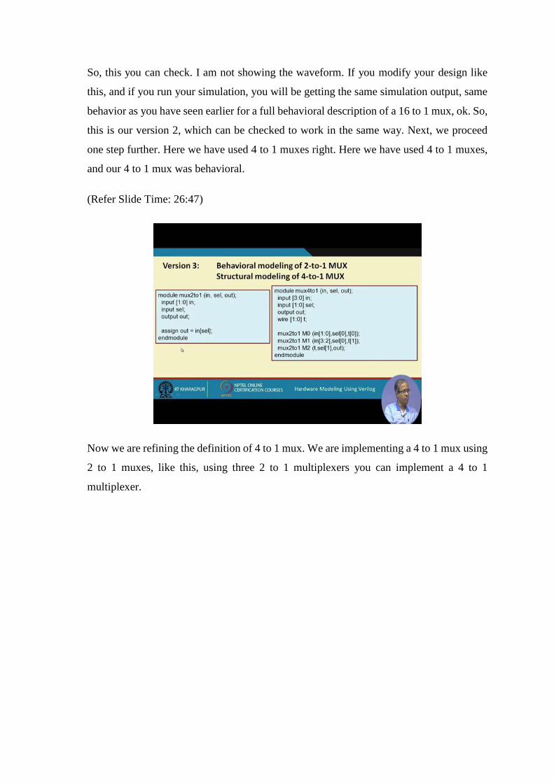
Now we are refining the definition of 4 to 1 mux. We are implementing a 4 to 1 mux using
2 to 1 muxes, like this, using three 2 to 1 multiplexers you can implement a 4 to 1
multiplexer.
(Refer Slide Time: 26:54)
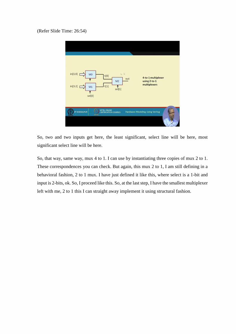
So, two and two inputs get here, the least significant, select line will be here, most
significant select line will be here.
So, that way, same way, mux 4 to 1. I can use by instantiating three copies of mux 2 to 1.
These correspondences you can check. But again, this mux 2 to 1, I am still defining in a
behavioral fashion, 2 to 1 mux. I have just defined it like this, where select is a 1-bit and
input is 2-bits, ok. So, I proceed like this. So, at the last step, I have the smallest multiplexer
left with me, 2 to 1 this I can straight away implement it using structural fashion.

(Refer Slide Time: 27:49)
So, a multiplexer, how does, means how do we implement a 2 to 1 mux.
(Refer Slide Time: 28:02)
The are 2 inputs, 1 input, and a select line. Let us say, the inputs are in0 and in1, this is sel
and the output is out. So, the way you can implement it is like this, you can take two AND
gates and an OR gate, this in0 can be connected here, this in1 can be connected here, and
this sel, you can connect directly here, and through an inverter here. So, when select is 0,
this will be 1, this, in0 will come out and when sel is 1 this will be 0, and this will be 1,

this in1 will be selected, in1 will be coming out, right. So, these are 4 gates. So, we specify
this structural description for the multiplexer, this is what we have described here, a NOT
gate, two AND gates and a OR gate.
So, whatever we have shown here is the typical design flow of a designer. So, when a
designer goes about designing a complex digital system. Well I have shown a relatively
very simple example so that you can appreciate, just a multiplexer, I have shown that we
start with using a behavioral description.
Then step by step hierarchically, we break it up into structural representation at various
levels, and when you are done. We have all the hierarchical descriptions all described in
the structural level, and what we have the overall design is a complete structural design,
ok. So, I strongly recommend that you should try out these examples yourself, run them
on a simulator, view the waveforms on GTK wave or any other tool that you have accessed
to, and you get a feel of this simulation and the feel of the design, ok.
So, we shall be continuing with some more examples in our next lectures again.
Thank you.