Embed Size (px)
Citation preview
Hardware Implementation of the OFDM and PPM
Transceiver for Under-Water Optical Wireless
Communication
by
Kanhaiya Mishra
EE16M024
A thesis submitted for the final year project of
MASTER OF TECHNOLOGY
with Communication and Signal Processing specialization in the
Department of Electrical Engineering
May 24, 2018
Thesis Certificate
This is to certify that the thesis titled Transceiver Implementation for Under-
Water Communication, submitted by Kanhaiya Mishra, to the Indian Institute
of Technology, Madras, for the award of the degree of Master of Technology in
Communication and Signal Processing, is a bonafide record of the research work
done by him under our supervision. The contents of this thesis, in full or in parts, have
not been submitted to any other Institute or University for the award of any degree or
diploma.
Prof. Deepa Venkitesh
M. Tech. Project Guide
Associate Professor
Dept. of Electrical Engineering
IIT-Madras, 600 036
Place: Chennai
Date: 21st May 2018
1

Acknowledgement
I would like to begin by thanking my project guide, Prof. Deepa Venkitesh for her
continuous support and extreme patience throughout my project. I would also like to
thank the principal investigator of the under-water communication project, Prof. Balaji
Srinivasan for his regular guidance in my project work and experiments. I would like to
extend special gratitude towards Prof. Radhakrishna Gantti for all his help in OFDM
simulation related studies and Prof. Harishankar Ramachandran for his guidance in
transceiver software programming and its hardware implementation.
I would also like to thank all my project team-mates from Fiber Laser Laboratory,
specially Pavitra, Bhuvna, Bastin and Prakash. Without their continuous hard work
and efforts, project experiments would not have been conducted successfully.
Lastly I would like to extend my thanks to my family whose support have kept
me going throughout my academic carrier. A special thanks to all my friends and
classmates specially Chirag, for their support and valuable knowledge sharing during
my complete Masters’ Program at IIT Madras.
2

Contents
1 Introduction 11
1.1 Aim of the Project . . . . . . . . . . . . . . . . . . . . . . . . . . . . . . 13
1.2 Previous Work Done . . . . . . . . . . . . . . . . . . . . . . . . . . . . . 15
2 System Design and Simulation 18
2.1 Block Diagram . . . . . . . . . . . . . . . . . . . . . . . . . . . . . . . . 18
2.2 Electrical Modulation: OFDM . . . . . . . . . . . . . . . . . . . . . . . 20
2.2.1 OFDM for Optical Intensity Modulation . . . . . . . . . . . . . . 23
2.2.2 Theoretical BER . . . . . . . . . . . . . . . . . . . . . . . . . . . 25
2.3 Electrical Modulation: PPM . . . . . . . . . . . . . . . . . . . . . . . . . 26
2.3.1 Demodulation and Theoretical BER . . . . . . . . . . . . . . . . 27
2.4 MATLAB Simulation . . . . . . . . . . . . . . . . . . . . . . . . . . . . . 28
2.5 Optical Amplification considerations in OFDM . . . . . . . . . . . . . . 30
3 Transceiver Hardware 34
3.1 Electrical Hardware . . . . . . . . . . . . . . . . . . . . . . . . . . . . . 34
3.1.1 Arbitrary Waveform Generation . . . . . . . . . . . . . . . . . . 34
3.1.2 Waveform Acquisition . . . . . . . . . . . . . . . . . . . . . . . . 39
3.2 Optical Sources . . . . . . . . . . . . . . . . . . . . . . . . . . . . . . . . 42
3.3 Optical Modulators . . . . . . . . . . . . . . . . . . . . . . . . . . . . . . 42
3.4 Auxiliary Driver Circuit . . . . . . . . . . . . . . . . . . . . . . . . . . . 45
3.5 Optical Detectors . . . . . . . . . . . . . . . . . . . . . . . . . . . . . . . 47
4 Transceiver Software 48
4.1 PPM Synchronization . . . . . . . . . . . . . . . . . . . . . . . . . . . . 48
4.2 OFDM Synchronization . . . . . . . . . . . . . . . . . . . . . . . . . . . 52
4.3 Frame Structure . . . . . . . . . . . . . . . . . . . . . . . . . . . . . . . 58
3
4.4 Transmitter Program Flow: . . . . . . . . . . . . . . . . . . . . . . . . . 60
4.5 Receiver Program Flow . . . . . . . . . . . . . . . . . . . . . . . . . . . 61
4.5.1 Demodulation Program Flow . . . . . . . . . . . . . . . . . . . . 63
4.5.2 BER Evaluation . . . . . . . . . . . . . . . . . . . . . . . . . . . 64
5 Test Results and Conclusion 65
5.1 Data Rates Achieved . . . . . . . . . . . . . . . . . . . . . . . . . . . . . 66
5.2 Experiment I: PPM-Optical Free-Space (520nm Laser with Direct Mod-
ulation): . . . . . . . . . . . . . . . . . . . . . . . . . . . . . . . . . . . . 66
5.3 Experiment II: PPM-Optical Back to Back using VOA (532nm LASER
I with EOM): . . . . . . . . . . . . . . . . . . . . . . . . . . . . . . . . . 70
5.4 Experiment III and IV: PPM and OFDM-Optical Back to Back using
VOA (532nm LASER II with EOM): . . . . . . . . . . . . . . . . . . . . 74
5.5 Conclusion: . . . . . . . . . . . . . . . . . . . . . . . . . . . . . . . . . . 82
5.6 Future Work: . . . . . . . . . . . . . . . . . . . . . . . . . . . . . . . . . 82
4

List of Figures
1.1 Electromagnetic absorption spectrum of earth’s atmosphere. . . . . . . . 11
1.2 Electromagnetic absorption spectrum of sea-water. . . . . . . . . . . . . 12
1.3 Comparison of acoustic, RF and optical wave communication technolo-
gies for under water communication . . . . . . . . . . . . . . . . . . . . 13
1.4 Transfer characteristics of the MZM external optical modulator used for
intensity modulation. . . . . . . . . . . . . . . . . . . . . . . . . . . . . . 16
1.5 Spectrum of OFDM signal before and after second harmonic generator. 17
1.6 Effect of square-root pre-compensation on the BER performance of OFDM
with SHG. . . . . . . . . . . . . . . . . . . . . . . . . . . . . . . . . . . . 17
2.1 Building blocks of the under-water communication system design . . . . 19
2.2 Bandwidth usage by FDM (a) and OFDM (b) for same amount of data
transmission. . . . . . . . . . . . . . . . . . . . . . . . . . . . . . . . . . 21
2.3 OFDM Transmitter and receiver block diagram. DC sub-carrier X0 may
or may not be used as required by the design. . . . . . . . . . . . . . . . 22
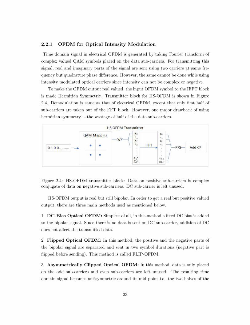
2.4 HS-OFDM transmitter block: Data on positive sub-carriers is complex
conjugate of data on negative sub-carriers. DC sub-carrier is left unused. 23
2.5 Antisymmetry property of the Fourier Transform . . . . . . . . . . . . . 24
2.6 Gray coded QAM-16 Constellation with average unit power per symbol. 25
2.7 16-PPM signal generation from binary data. . . . . . . . . . . . . . . . 26
2.8 Bit error rate performance of PPM. As the order increases, BER im-
proves by log10(L2 log2 L
)dB . . . . . . . . . . . . . . . . . . . . . . . . 29
2.9 Bit error rate performance of optical OFDM schemes. DCO-OFDM has
the worst performance. . . . . . . . . . . . . . . . . . . . . . . . . . . . . 30
2.10 Amplitude probability distribution of DCO, FLIP and ACO -OFDM
schemes with QAM-4 symbol mapping. . . . . . . . . . . . . . . . . . . . 31
5

2.11 Gain characteristics of an optical amplifier with respect to increasing
signal power [6]. . . . . . . . . . . . . . . . . . . . . . . . . . . . . . . . 31
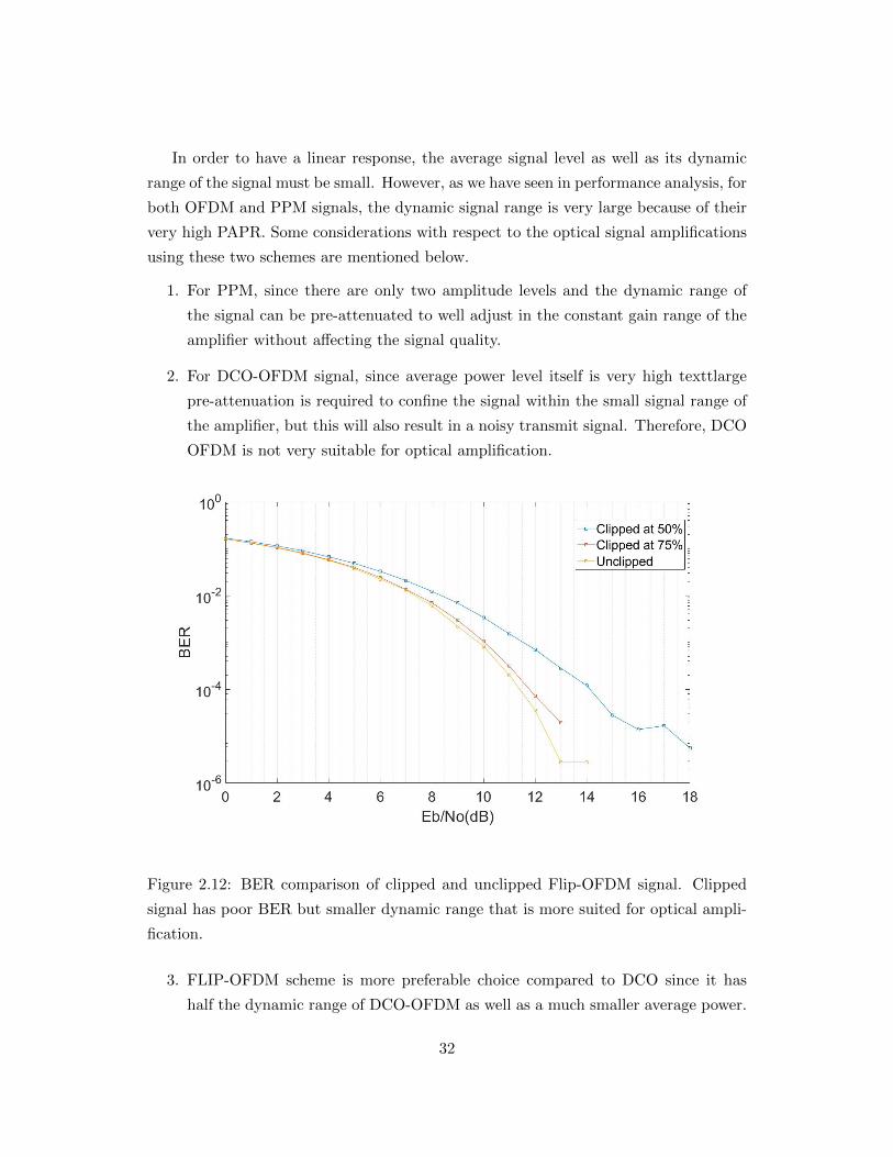
2.12 BER comparison of clipped and unclipped Flip-OFDM signal. Clipped
signal has poor BER but smaller dynamic range that is more suited for
optical amplification. . . . . . . . . . . . . . . . . . . . . . . . . . . . . . 32
3.1 Electrical Board: RedPitaya STEM-LAB, comes with two 14bit-DACs
and ADCs (SMA ports) each capable of running at 125Msps. . . . . . . 35
3.2 Arbitrary waveform output of the sample code using continuous mode. . 36
3.3 Arbitrary waveform output of the sample code using continuous mode. . 37
3.4 Output waveform in streaming mode, consecutive streams(frames) are
distinguished by its amplitude which is set to be (frm no%20) + 5)/25
in the program. . . . . . . . . . . . . . . . . . . . . . . . . . . . . . . . . 39
3.5 Probability distribution of time taken to write one full signal buffer.
Profiling of the C code was done using ’clock()’ function. . . . . . . . . . 40
3.6 Diffraction of light beam causing change in the intensity when a sound
wave travels in an acousto-optic crystal [6]. . . . . . . . . . . . . . . . . 43
3.7 Intensity Modulation using an electro-optic crystal between two aligned
polarisers. . . . . . . . . . . . . . . . . . . . . . . . . . . . . . . . . . . . 44
3.8 Intensity modulation by using the EOM Crystal in Mach-Zehnder Inter-
ferometer. The setup is called Mach-Zehnder Modulator [6]. . . . . . . . 45
3.9 Combined driver circuit for Direct modulation on 520nm Laser, pre-
amplifier for EOM and pre-amplifier for AOM. . . . . . . . . . . . . . . 46
4.1 Sliding window correlation of PPM signal. Eb/No = 3dB, PPM Order
= 8, Sync sequence length 32, Oversampling = 8. . . . . . . . . . . . . . 49
4.2 Sliding window correlation using faster computation method. Simulation
parameters same as given in figure 4.1. . . . . . . . . . . . . . . . . . . . 50
4.3 OFDM sync point detection by finding maximum of window minimum
of correlation factor. . . . . . . . . . . . . . . . . . . . . . . . . . . . . . 53
4.4 False peak in OFDM synchronization in presence of DC component in
the noise samples before pilot symbol. . . . . . . . . . . . . . . . . . . . 55
4.5 Effect of oversampling on mean synchronization error. Oversampling is
more advantageous at low SNR. . . . . . . . . . . . . . . . . . . . . . . . 57
6

4.6 Continuous acquisition of samples from ADC to a local buffer and their
simultaneous demodulation. Undemodulated samples from previous cy-
cle are carried forward to next execution cycle. . . . . . . . . . . . . . . 62
5.1 Free space communication block diagram. Source/modulators may change
in different test setups. . . . . . . . . . . . . . . . . . . . . . . . . . . . . 65
5.2 Free Space Optical setup using directly modulated 520nm semiconductor
laser. . . . . . . . . . . . . . . . . . . . . . . . . . . . . . . . . . . . . . . 67
5.3 LI characteristics of 520nm Laser diode depicting direct modulation with
80mA bias and 30mA swing. . . . . . . . . . . . . . . . . . . . . . . . . 68
5.4 BER vs Received Power for 4-PPM directly modulated 520nm LASER
in Free-space . . . . . . . . . . . . . . . . . . . . . . . . . . . . . . . . . 69
5.5 Complete experimental setup with all electrical and optical components
used in experiments II, III and IV. . . . . . . . . . . . . . . . . . . . . . 70
5.6 Optical Back to back setup using VOA to vary the optical power. . . . . 71
5.7 External optical modulator characteristics with 532nm LASER I. Bias
point of modulation signal was adjusted such the average power remains
same. . . . . . . . . . . . . . . . . . . . . . . . . . . . . . . . . . . . . . 71
5.8 PDA-100A-EC Photo detector conversion characteristics at 10dB gain
and 1.4MHz bandwidth setting. . . . . . . . . . . . . . . . . . . . . . . . 72
5.9 BER vs Received Power for 4-PPM externally modulated 532nm LASER
I in optical back to back configuration . . . . . . . . . . . . . . . . . . . 73
5.10 External optical modulator characteristics with 532nm LASER II at
1.70Amp bias current. . . . . . . . . . . . . . . . . . . . . . . . . . . . . 74
5.11 PDA-100A-EC Photo detector conversion characteristics at 0dB gain
and 2.4MHz bandwidth setting. . . . . . . . . . . . . . . . . . . . . . . . 75
5.12 Constellation plot of 16-QAM OFDM signal at 9.24uW and 14.20uW
average received power. . . . . . . . . . . . . . . . . . . . . . . . . . . . 76
5.13 Synchronized signal for DCO-OFDM using 16-QAM. ADC quantization
noise as well as some ADC DC offset error is clearly visible. . . . . . . . 77
5.14 Synchronization of 16QAM OFDM signal at 9.24uW received power.
Peak of window minimum plot identifies the sync point, as explained
earlier in the chapter. . . . . . . . . . . . . . . . . . . . . . . . . . . . . 77
5.15 BER vs Received Power curves for DCO-OFDM QAM-4 and QAM-16. . 78
5.16 4-PPM signal waveform at 44uW received power. . . . . . . . . . . . . . 79
7
5.17 16-PPM signal waveform at 14uW received power. . . . . . . . . . . . . 80
5.18 BER vs Received Power curves for L-PPM modulation for L=4,8,16. . . 80
5.19 Under development test-bed for under-water experiments in the Wave
Flume facility of Ocean Engineering Department. . . . . . . . . . . . . . 83
8
List of Tables
2.1 Performance comparison of Optical-OFDM schemes with respect to elec-
trical OFDM. . . . . . . . . . . . . . . . . . . . . . . . . . . . . . . . . . 24
2.2 Code-words of different PPM variants . . . . . . . . . . . . . . . . . . . 27
3.1 Key specifications of the optical detectors used for direct detection. . . . 47
4.1 PPM and OFDM frame structure in terms of number of samples. . . . . 60
5.1 Data Rates for PPM and OFDM modulation schemes. For number of
symbols per frame see Frame structure in Chapter 4. . . . . . . . . . . . 66
5.2 BER at different received power levels with varying distance between
transmitter and receiver for 4-PPM modulation. . . . . . . . . . . . . . 68
5.3 BER at different power levels with varying attenuation using VOA for
4-PPM modulation. . . . . . . . . . . . . . . . . . . . . . . . . . . . . . 72
5.4 BER values at different average received optical power levels for DCO-
OFDM using QAM-4 and QAM-16 mapping. . . . . . . . . . . . . . . . 76
5.5 BER values at different average received opitcal power levels for L-PPM
using three different values of L = {4,8,16}. . . . . . . . . . . . . . . . . 79
9

List of Abbreviations
RF Radio Frequency
LOS Line of Sight
PPM Pulse Position Modulation
DPPM Differential PPM
DPIM Digital Pule interval Modulation
DHPIM Dual Header Pule interval Modulation
DAPPM Dual Amplitude Pulse Position Modulation
FDM Frequency Division Multiplexing
OFDM Orthogonal Frequency Division Multiplexing
DCO-OFDM DC Bias Optical OFDM
ACO-OFDM Asymmetrically Clipped Optical OFDM
QAM Quadrature Amplitude Multiplexing
SER Symbol Error Rate
BER Bit Error Rate
FFT Fast Fourier Transform
CP Cyclic Prefix
DSC Data Sub-Carriers
DAC Digital to Analog Converter
ADC Analog to Digital Converter
EOM Electro-optic modulator
AOM Acousto-optic modulator
MZM Mach Zehnder Modulator
OOK-NRZ On-off Keying Non-Return to Zero
PRBS Pseudo Random Binary Sequence
PN-Sequence Pseudo Noise Sequence
VOA Variable Optical Attenuator
10
Chapter 1
Introduction
In recent times, the interest in the field of wireless optical communication has im-
mensely increased because of its potential bandwidth advantages. Utilizing the optical
carriers even under simplest modulation schemes gives better data rates than achieved
by radio frequency based wireless communication. Unlike radio frequency, optical car-
riers do not require any licensing and can be used freely. However, wireless optical
communication has its disadvantages as well when compared to the radio-frequency.
Use of this technology for terrestrial and under-water applications has been discussed
below.
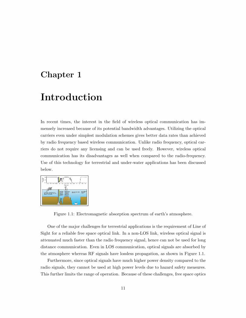
Figure 1.1: Electromagnetic absorption spectrum of earth’s atmosphere.
One of the major challenges for terrestrial applications is the requirement of Line of
Sight for a reliable free space optical link. In a non-LOS link, wireless optical signal is
attenuated much faster than the radio frequency signal, hence can not be used for long
distance communication. Even in LOS communication, optical signals are absorbed by
the atmosphere whereas RF signals have lossless propagation, as shown in Figure 1.1.
Furthermore, since optical signals have much higher power density compared to the
radio signals, they cannot be used at high power levels due to hazard safety measures.
This further limits the range of operation. Because of these challenges, free space optics
11

is relatively less explored technology in the field of wireless communication.
Nevertheless some visible light communication links have been deployed successfully
for indoor communications. Even the next generation mobile communication technol-
ogy is aiming to harness its potential bandwidth advantages by using optical signals at
specific places in the link.
In a more preferable under-water scenario where optical signals suffer the least
attenuation among all electromagnetic waves, use of wireless optics for high data rate
communication is a more favourable option. Absorption spectrum of the sea-water is
shown in figure 1.2. The blue-green region of the visible light window has the smallest
absorption coefficient.
Figure 1.2: Electromagnetic absorption spectrum of sea-water.
Presently, acoustic wave communication is the widely adopted method for under-
water communication links since it provides a much longer range. However, acoustic
waves can avail only modest data rates, hence is not the best alternative with the
increasing demand of data transfer. The other option to use radio frequencies for high
data rates requires the under-water vehicle to resurface on the water since RF signal
is highly attenuated by the water. Therefore, with decent propagation characteristics
12
both in the open atmosphere and under-water makes wireless optics a much likely
choice for the under-water to above surface communication links. Furthermore, optical
system design requires much smaller equipments on board as compared to the acoustic
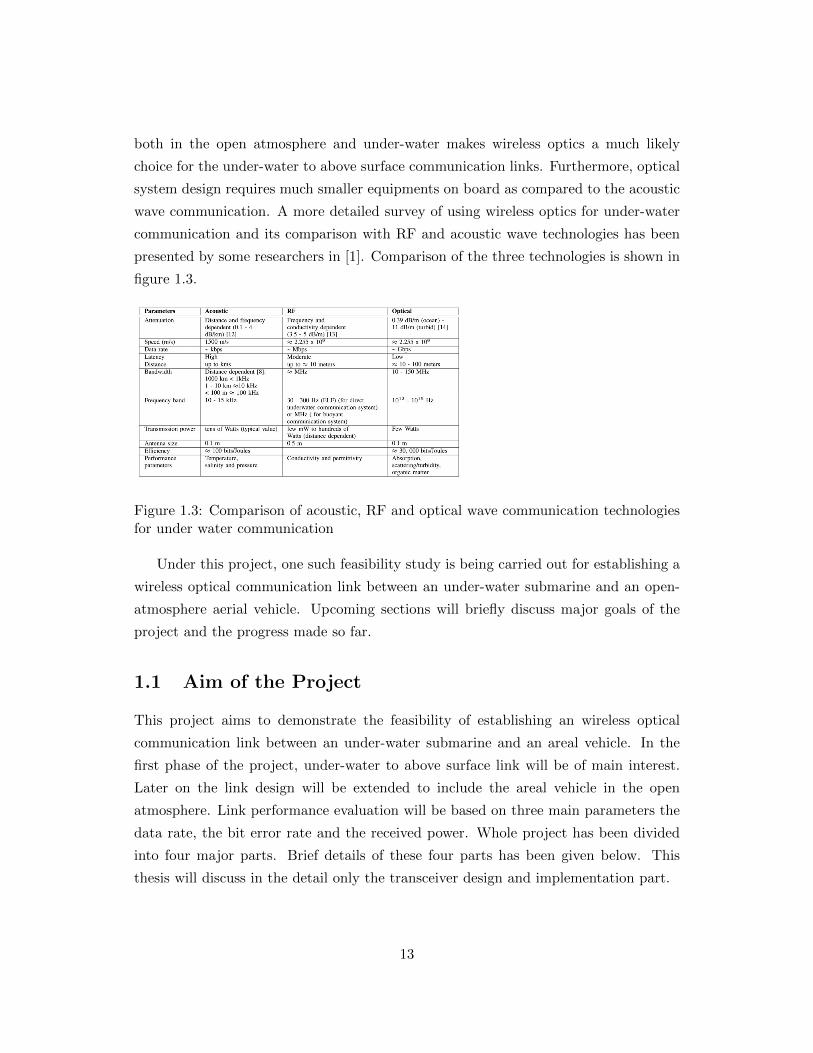
wave communication. A more detailed survey of using wireless optics for under-water
communication and its comparison with RF and acoustic wave technologies has been
presented by some researchers in [1]. Comparison of the three technologies is shown in
figure 1.3.
Figure 1.3: Comparison of acoustic, RF and optical wave communication technologiesfor under water communication
Under this project, one such feasibility study is being carried out for establishing a
wireless optical communication link between an under-water submarine and an open-
atmosphere aerial vehicle. Upcoming sections will briefly discuss major goals of the
project and the progress made so far.
1.1 Aim of the Project
This project aims to demonstrate the feasibility of establishing an wireless optical
communication link between an under-water submarine and an areal vehicle. In the
first phase of the project, under-water to above surface link will be of main interest.
Later on the link design will be extended to include the areal vehicle in the open
atmosphere. Link performance evaluation will be based on three main parameters the
data rate, the bit error rate and the received power. Whole project has been divided
into four major parts. Brief details of these four parts has been given below. This
thesis will discuss in the detail only the transceiver design and implementation part.
13
1. Sea-Water Characterization: This part focuses on the absorption and scattering
loss characterization of the actual deep sea water. Experiments have been conducted
in the bay of Bengal at different locations and at different times of the year to get this
data for visible wavelength optical sources. Based on the experiments, 532nm has been
identified as the best suitable wavelength for the link.
2. Channel Estimation: Using the absorption and scattering field data, actual sea
conditions are simulated and a channel model is created. This model will be later used
understanding the propagation of light waves in the deep sea-water and based on that
channel coding will be implemented. This channel model is still under development.
3. Optical Source Design: For the identified optimum wavelength, 532nm, a high
power indigenous optical source is being developer. This source uses a seed infra-red
laser, an optical power amplifier and a second-harmonic generator to get the desired
532nm wavelength. Once the transceiver design is ready, it will be tested using this
source, appropriate modifications will be made.
4. Transceiver Design: This part is main focus of the thesis. The actual communi-
cation link design and implementation has been discussed in detail. Main goal for this
part of the project is to implement the two specific modulation schemes Pulse Position
Modulation and Orthogonal Frequency Division Multiplexing and compare their per-
formance for the under-water communication link. Performance comparison has been
done in the software simulation as well as on the actual hardware.
Next section in this chapter will briefly explain the previous work done and the
expected outcome of this part of the project.
In the second chapter of this thesis, details of the modulation schemes and their
software simulations will be presented. Expected performance of two schemes will be
discussed as well.
Third chapter will provide the details of the Hardware components used for the
implementing the transceiver design. Details of both the electrical and the optical
hardware has been presented.
Fourth chapter describes in detail the software written for implementing the trans-
mitter and the receiver of the two modulation schemes . Major part of this chapter
is dedication to the receiver synchronization and the challenges in the practical imple-
mentation.
14
The penultimate chapter presents the results of the experiments conducted using
the designed transceiver and concludes the thesis with the performance evaluation of
the OFDM and PPM modulation formats.
1.2 Previous Work Done
Earlier under this project, major work has been done on studying the non-linearities
introduced by the transmitter design and develop a pre-compensation scheme to miti-
gate the effect of these non-linearities. There are two major sources of non-linearity in
the system.
1. Second Harmonic Generator: Optical source design which includes a sec-
ond harmonic generator to generate the blue-green wavelength from an amplified
infra-red source is a non-linear element. The modulated signal from the infra-red
source when passed through SHG gets distorted.
2. External Modulator: Mach-Zehnder intensity modulator being used for the
system design has sinusoidal transfer characteristics as shown in figure 1.4. De-
pending on the bias point of the modulator and peak to peak swing of the input
signal, there will be some non-linear distortion in the intensity modulated optical
signal.
For pulse-position modulation format, there was no effect on the performance since
the output signal has only two levels. For a threshold based demodulation, the non-
linearities mentioned above will only require a change of threshold for getting the same
performance, which will anyway be adjusted based on the received signal level.
For orthogonal frequency modulation format, major non-linearity came from the
second harmonic generator(SHG) and resulted in the distortion of the spectrum of the
transmit signal as shown in figure 1.4.
For non-linearity from the modulator, two cases of quadrature and non-quadrature
bias points of the EOM were considered. For small swing of the input signal, transfer
characteristics of the MZM under quadrature bias can be approximated to be linear. For
any other bias point, more or less non-linearities would arise depending on the actual
bias point. However, finding a closed form analytical expression to correct for those
non-linearities was very complex. For the simulations, square root pre-compensation
was used to at least correct the non-linearities from the SHG for all bias cases.
15
Figure 1.4: Transfer characteristics of the MZM external optical modulator used forintensity modulation.
Data transfer experiments were conducted using the USRP board with a directly
modulated red laser. Pre-generated samples were transmitted and acquired via a short
distance free space link. The acquired samples were post-processed to calculate the
bit error rate performance. To continue the same work in a more real environment, a
fresh transceiver design was implemented on a different board (details are mentioned
in Chapter 4 and 5). Under the new design, demodulation and modulation was done
in real-time unlike in the previous work.
16
Figure 1.5: Spectrum of OFDM signal before and after second harmonic generator.
Figure 1.6: Effect of square-root pre-compensation on the BER performance of OFDMwith SHG.
17
Chapter 2
System Design and Simulation
This chapter explains the building blocks of the over all system design. Implementation
details of both the modulation formats PPM and OFDM are presented in detail. A
simulation model is given to test the bit error rate performance of the two schemes using
MATLAB software. Based on the BER performance, advantages and disadvantages of
using each have been discussed.
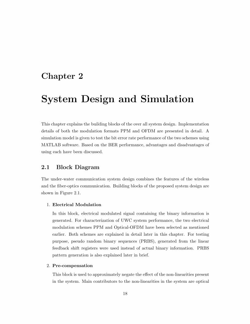
2.1 Block Diagram
The under-water communication system design combines the features of the wireless
and the fiber-optics communication. Building blocks of the proposed system design are
shown in Figure 2.1.
1. Electrical Modulation
In this block, electrical modulated signal containing the binary information is
generated. For characterization of UWC system performance, the two electrical
modulation schemes PPM and Optical-OFDM have been selected as mentioned
earlier. Both schemes are explained in detail later in this chapter. For testing
purpose, pseudo random binary sequences (PRBS), generated from the linear
feedback shift registers were used instead of actual binary information. PRBS
pattern generation is also explained later in brief.
2. Pre-compensation
This block is used to approximately negate the effect of the non-linearities present
in the system. Main contributors to the non-linearities in the system are optical
18
Figure 2.1: Building blocks of the under-water communication system design
modulator and second harmonic generator as also mentioned earlier. Since the
source design involving the SHG is not yet complete, no compensator is required
in the current implementation.
3. Intensity Modulation
This block generates the intensity modulated optical signal based on the input
electrical signal. For the current implementation, both external and direct mod-
ulation schemes were used with different optical sources to generate the intensity
modulated signal. For external optical modulator, its bias and the input signal
was adjusted for minimum non-linearities in the optical output to obviate the
need of any compensator. Detailed characterization of the optical modulators
and optical sources is presented in chapter 4.
4. Second Harmonic Generator
The optical source chosen for the system is the green laser (532nm) considering
its very low absorption under sea-water. Finding a directly emitting very high
power green-laser is not very easy. Therefore, a more preferable choice is to use
an amplified infra-red source at 1064nm and use a second harmonic generator
to get the desired wavelength. Since the optical source design using SHG is still
under progress, this block has not been used in the current implementation.
19
5. Under-Water Channel
The intensity modulated optical signal propagates through under-water chan-
nel. Actual implementation does not use this block. However, to understand
the propagation of green light through sea-water, a separate channel model is
being developed. For the experiment purpose, free space channel and back-to-
back channel with a variable optical attenuator have been used. Nevertheless,
few initial experiments were conducted in a wave-flume facility in the Ocean En-
gineering Department at IIT Madras to study and incorporate the actual channel
behaviour in the system design. Details of the experiments and test results are
mentioned in Chapter 6.
6. Direct Detection
This block converts the optical signal back to the electrical signal using the photo-
detectors. Simplicity of using direct detection is that it has a linear conversion
from optical intensity to the electrical current (voltage). For the current im-
plementation, Silicon based photo-detectors with on-board TIA have been used.
Conversion characteristics of the detectors are mentioned in chapter 4.
7. Demodulation and BER Evaluation
This constitutes the the major portion of the receiver design. In this block, the
received signal is synchronized and demodulated and the demodulated binary
data is then compared to the originally sent data to calculate the bit error rate
(BER). BER vs SNR performance for fixed transmitter bandwidth is used to
decide which modulation scheme is better. Synchronization methods for both
modulation formats are discussed in detail in chapter 5.
2.2 Electrical Modulation: OFDM
In wireless, frequency division multiplexing (FDM) technique is used to send the data
over different carrier frequencies simultaneously. To avoid the interference among the
different carriers, some guard band is left between adjacent sub-carriers. This tradi-
tional version of FDM results in wastage of available spectrum bandwidth.
A new FDM technique which maximizes the spectrum utilization by sending the
data over equally spaced multiple orthogonal sub-carrier frequencies is called OFDM.
20
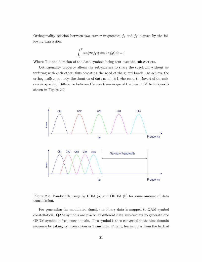
Orthogonality relation between two carrier frequencies f1 and f2 is given by the fol-
lowing expression. ∫ T
0sin(2πf1t) sin(2πf2t)dt = 0
Where T is the duration of the data symbols being sent over the sub-carriers.
Orthogonality property allows the sub-carriers to share the spectrum without in-
terfering with each other, thus obviating the need of the guard bands. To achieve the
orthogonality property, the duration of data symbols is chosen as the invert of the sub-
carrier spacing. Difference between the spectrum usage of the two FDM techniques is
shown in Figure 2.2.
Figure 2.2: Bandwidth usage by FDM (a) and OFDM (b) for same amount of datatransmission.
For generating the modulated signal, the binary data is mapped to QAM symbol
constellation. QAM symbols are placed at different data sub-carriers to generate one
OFDM symbol in frequency domain. This symbol is then converted to the time domain
sequence by taking its inverse Fourier Transform. Finally, few samples from the back of
21

sequence are added in front, called cyclic prefix and resulting sequence is transmitted.
For demodulation, all these steps are followed in reverse direction to get the original
binary data. Some of the key concepts in OFDM are mentioned in [2]. A block diagram
of OFDM transceiver is presented in figure 2.3.
Figure 2.3: OFDM Transmitter and receiver block diagram. DC sub-carrier X0 mayor may not be used as required by the design.
Cyclic Prefix: Cyclic prefix plays a crucial role in OFDM. It provides robustness to
the OFDM signal in a multipath fading channel. Length of the prefix is chosen larger
than the length of the channel response. Two major advantages of adding the cyclic
prefix are given below.
1. ISI Reduction: In a multi-path fading channel, the convolution of the transmit
signal with channel results in inter-symbol interference (ISI) at the receiver. Ad-
dition of cyclic prefix of a larger length than the channel response eliminates this
ISI by isolating the convolution of the adjacent symbols from each other.
2. Single Tap Equalization: With addition of CP, any linear shift of length
smaller than the CP length becomes circular shift. This turns the linear convolu-
tion into circular convolution thus enabling linear channel equalization as shown
in the following expressions.
22
2.2.1 OFDM for Optical Intensity Modulation
Time domain signal in electrical OFDM is generated by taking Fourier transform of
complex valued QAM symbols placed on the data sub-carriers. For transmitting this
signal, real and imaginary parts of the signal are sent using two carriers at same fre-
quency but quadrature phase difference. However, the same cannot be done while using
intensity modulated optical carriers since intensity can not be complex or negative.
To make the OFDM output real valued, the input OFDM symbol to the IFFT block
is made Hermitian Symmetric. Transmitter block for HS-OFDM is shown in Figure
2.4. Demodulation is same as that of electrical OFDM, except that only first half of
sub-carriers are taken out of the FFT block. However, one major drawback of using
hermitian symmetry is the wastage of half of the data sub-carriers.
Figure 2.4: HS-OFDM transmitter block: Data on positive sub-carriers is complexconjugate of data on negative sub-carriers. DC sub-carrier is left unused.
HS-OFDM output is real but still bipolar. In order to get a real but positive valued
output, there are three main methods used as mentioned below.
1. DC-Bias Optical OFDM: Simplest of all, in this method a fixed DC bias is added
to the bipolar signal. Since there is no data is sent on DC sub-carrier, addition of DC
does not affect the transmitted data.
2. Flipped Optical OFDM: In this method, the positive and the negative parts of
the bipolar signal are separated and sent in two symbol durations (negative part is
flipped before sending). This method is called FLIP-OFDM.
3. Asymmetrically Clipped Optical OFDM: In this method, data is only placed
on the odd sub-carriers and even sub-carriers are left unused. The resulting time
domain signal becomes antisymmetric around its mid point i.e. the two halves of the
23
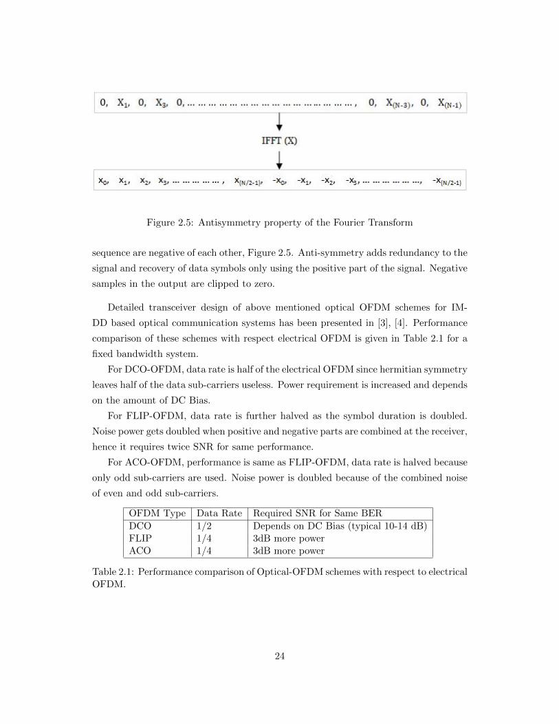
Figure 2.5: Antisymmetry property of the Fourier Transform
sequence are negative of each other, Figure 2.5. Anti-symmetry adds redundancy to the
signal and recovery of data symbols only using the positive part of the signal. Negative
samples in the output are clipped to zero.
Detailed transceiver design of above mentioned optical OFDM schemes for IM-
DD based optical communication systems has been presented in [3], [4]. Performance
comparison of these schemes with respect electrical OFDM is given in Table 2.1 for a
fixed bandwidth system.
For DCO-OFDM, data rate is half of the electrical OFDM since hermitian symmetry
leaves half of the data sub-carriers useless. Power requirement is increased and depends
on the amount of DC Bias.
For FLIP-OFDM, data rate is further halved as the symbol duration is doubled.
Noise power gets doubled when positive and negative parts are combined at the receiver,
hence it requires twice SNR for same performance.
For ACO-OFDM, performance is same as FLIP-OFDM, data rate is halved because
only odd sub-carriers are used. Noise power is doubled because of the combined noise
of even and odd sub-carriers.
OFDM Type Data Rate Required SNR for Same BER
DCO 1/2 Depends on DC Bias (typical 10-14 dB)FLIP 1/4 3dB more powerACO 1/4 3dB more power
Table 2.1: Performance comparison of Optical-OFDM schemes with respect to electricalOFDM.
24
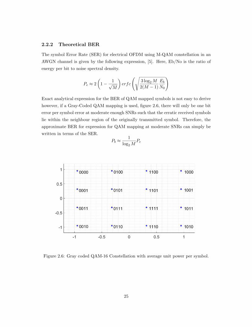
2.2.2 Theoretical BER
The symbol Error Rate (SER) for electrical OFDM using M-QAM constellation in an
AWGN channel is given by the following expression, [5]. Here, Eb/No is the ratio of
energy per bit to noise spectral density.
Pe ≈ 2
(1− 1√
M
)erfc
(√3 log2M
2(M − 1)
Eb
N0
)
Exact analytical expression for the BER of QAM mapped symbols is not easy to derive
however, if a Gray-Coded QAM mapping is used, figure 2.6, there will only be one bit
error per symbol error at moderate enough SNRs such that the erratic received symbols
lie within the neighbour region of the originally transmitted symbol. Therefore, the
approximate BER for expression for QAM mapping at moderate SNRs can simply be
written in terms of the SER.
Pb ≈1
log2MPe
Figure 2.6: Gray coded QAM-16 Constellation with average unit power per symbol.
25
2.3 Electrical Modulation: PPM
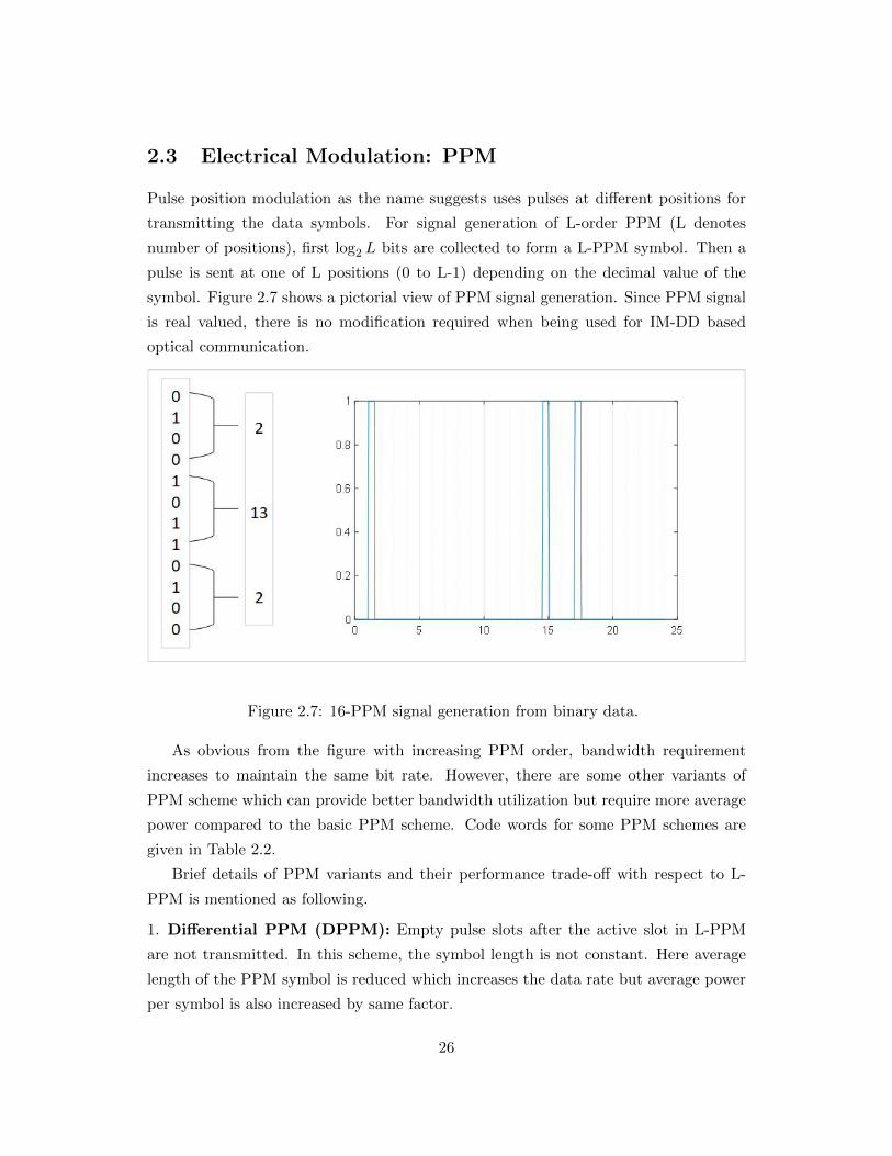
Pulse position modulation as the name suggests uses pulses at different positions for
transmitting the data symbols. For signal generation of L-order PPM (L denotes
number of positions), first log2 L bits are collected to form a L-PPM symbol. Then a
pulse is sent at one of L positions (0 to L-1) depending on the decimal value of the
symbol. Figure 2.7 shows a pictorial view of PPM signal generation. Since PPM signal
is real valued, there is no modification required when being used for IM-DD based
optical communication.
Figure 2.7: 16-PPM signal generation from binary data.
As obvious from the figure with increasing PPM order, bandwidth requirement
increases to maintain the same bit rate. However, there are some other variants of
PPM scheme which can provide better bandwidth utilization but require more average
power compared to the basic PPM scheme. Code words for some PPM schemes are
given in Table 2.2.
Brief details of PPM variants and their performance trade-off with respect to L-
PPM is mentioned as following.
1. Differential PPM (DPPM): Empty pulse slots after the active slot in L-PPM
are not transmitted. In this scheme, the symbol length is not constant. Here average
length of the PPM symbol is reduced which increases the data rate but average power
per symbol is also increased by same factor.
26
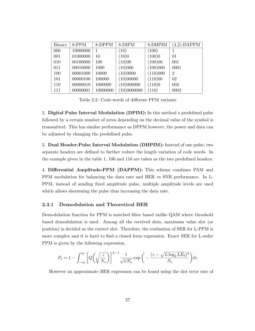
Binary 8-PPM 8-DPPM 8-DIPM 8-DHPIM (4,2)-DAPPM
000 10000000 1 (10) (100) 1001 01000000 10 (10)0 (100)0 01010 00100000 100 (10)00 (100)00 001011 00010000 1000 (10)000 (100)000 0001100 00001000 10000 (10)0000 (110)000 2101 00000100 100000 (10)00000 (110)00 02110 00000010 1000000 (10)000000 (110)0 002111 00000001 10000000 (10)0000000 (110) 0002
Table 2.2: Code-words of different PPM variants
2. Digital Pulse Interval Modulation (DPIM): In this method a predefined pulse
followed by a certain number of zeros depending on the decimal value of the symbol is
transmitted. This has similar performance as DPPM however, the power and data can
be adjusted by changing the predefined pulse.
3. Dual Header-Pulse Interval Modulation (DHPIM): Instead of one pulse, two
separate headers are defined to further reduce the length variation of code words. In
the example given in the table 1, 100 and 110 are taken as the two predefined headers.
4. Differential Amplitude-PPM (DAPPM): This scheme combines PAM and
PPM modulation for balancing the data rate and BER vs SNR performance. In L-
PPM, instead of sending fixed amplitude pulse, multiple amplitude levels are used
which allows shortening the pulse thus increasing the data rate.
2.3.1 Demodulation and Theoretical BER
Demodulation function for PPM is matched filter based unlike QAM where threshold
based demodulation is used. Among all the received slots, maximum value slot (or
position) is decided as the correct slot. Therefore, the evaluation of SER for L-PPM is
more complex and it is hard to find a closed form expression. Exact SER for L-order
PPM is given by the following expression.
Pe = 1−∫ ∞−∞
[Q
(√z
No
)]L−1 1√πNo
exp
(−
(z −√L log2 LEb)
2
No
)dz
However an approximate BER expression can be found using the slot error rate of
27
symbols and is given as following.
Pb ≈L
2
[1
2erfc
(√(L2 log2 L)Eb
No
)]L/2 factor denotes approximate average number of bit errors per slot error, a more
accurate result can be found by using the exact expression for this factor.
2.4 MATLAB Simulation
For comparison of the performance of the two modulation schemes, simulations were
conducted in MATLAB for a fixed sampling rate on the transmitter. Both methods
were compared against a common reference, the most basic modulation BPSK scheme.
Simulation model uses a simple Additive White Gaussian Noise based channel model.
Simulation Parameters: Sampling parameters chosen for both the schemes are
listed below. Also some OFDM specific parameters are also given.
1. Sample Rate = 1Msps, Over Sampling = 1, Sample Duration = 1us
2. Channel = AWGN, Data Modulation = 4-QAM
3. FFT Size = 1024, Data Sub Carriers (DSC) = 720, CP = 64
BER Performance: BER plots for PPM and OFDM schemes are shown in figure
2.8 and 2.9 respectively. For PPM, higher the order of PPM better the performance i.e.
power requirement goes down. For OFDM, FLIP and ACO require much less power
as compared to DCO scheme where the DC power is simply wasted. If we increase
the QAM order (BER plot only shows QAM-4), more power is required by all OFDM
schemes to maintain their BER performance (see the M-QAM BER expression).
Data Rate Performance: Bit rate calculations are shown as below. For OFDM,
log2M ∗ DSC bits are transmitted using FFT + CP samples. For PPM, log2 L bits
are transmitted using L samples. Higher the PPM order, smaller the data rate whereas
OFDM with higher order QAM gives higher data rate.
• Reference BPSK: (1/10−6) = 1Mbps
28
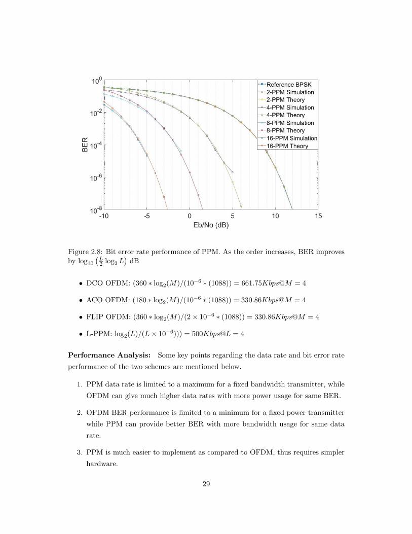
Figure 2.8: Bit error rate performance of PPM. As the order increases, BER improvesby log10
(L2 log2 L
)dB
• DCO OFDM: (360 ∗ log2(M)/(10−6 ∗ (1088)) = 661.75Kbps@M = 4
• ACO OFDM: (180 ∗ log2(M)/(10−6 ∗ (1088)) = 330.86Kbps@M = 4
• FLIP OFDM: (360 ∗ log2(M)/(2× 10−6 ∗ (1088)) = 330.86Kbps@M = 4
• L-PPM: log2(L)/(L× 10−6))) = 500Kbps@L = 4
Performance Analysis: Some key points regarding the data rate and bit error rate
performance of the two schemes are mentioned below.
1. PPM data rate is limited to a maximum for a fixed bandwidth transmitter, while
OFDM can give much higher data rates with more power usage for same BER.
2. OFDM BER performance is limited to a minimum for a fixed power transmitter
while PPM can provide better BER with more bandwidth usage for same data
rate.
3. PPM is much easier to implement as compared to OFDM, thus requires simpler
hardware.
29
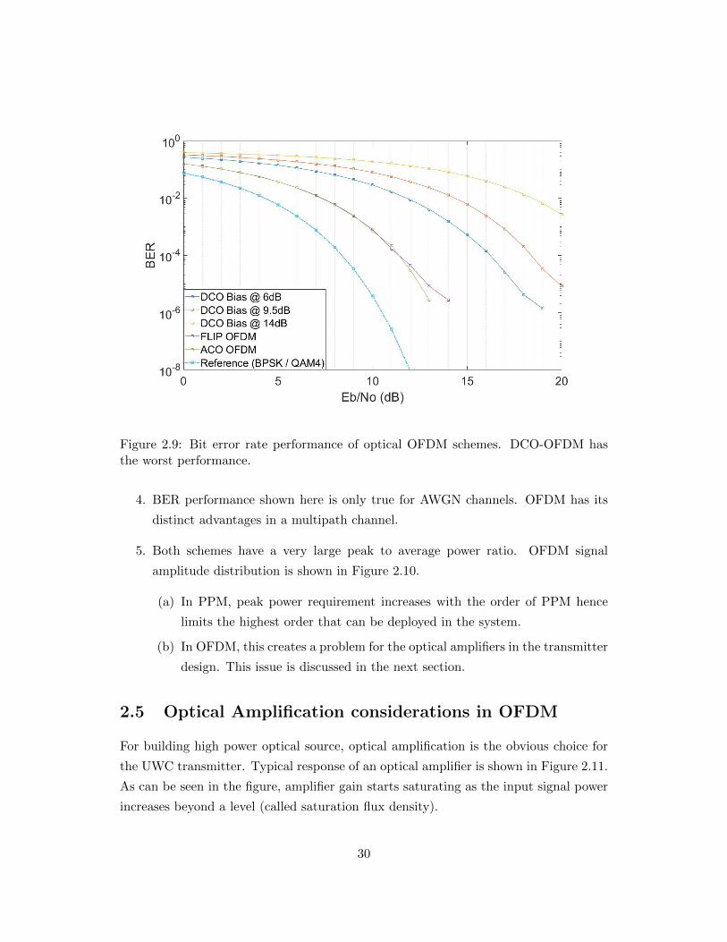
Figure 2.9: Bit error rate performance of optical OFDM schemes. DCO-OFDM hasthe worst performance.
4. BER performance shown here is only true for AWGN channels. OFDM has its
distinct advantages in a multipath channel.
5. Both schemes have a very large peak to average power ratio. OFDM signal
amplitude distribution is shown in Figure 2.10.
(a) In PPM, peak power requirement increases with the order of PPM hence
limits the highest order that can be deployed in the system.
(b) In OFDM, this creates a problem for the optical amplifiers in the transmitter
design. This issue is discussed in the next section.
2.5 Optical Amplification considerations in OFDM
For building high power optical source, optical amplification is the obvious choice for
the UWC transmitter. Typical response of an optical amplifier is shown in Figure 2.11.
As can be seen in the figure, amplifier gain starts saturating as the input signal power
increases beyond a level (called saturation flux density).
30

Figure 2.10: Amplitude probability distribution of DCO, FLIP and ACO -OFDM
schemes with QAM-4 symbol mapping.
Figure 2.11: Gain characteristics of an optical amplifier with respect to increasing
signal power [6].31
In order to have a linear response, the average signal level as well as its dynamic
range of the signal must be small. However, as we have seen in performance analysis, for
both OFDM and PPM signals, the dynamic signal range is very large because of their
very high PAPR. Some considerations with respect to the optical signal amplifications
using these two schemes are mentioned below.
1. For PPM, since there are only two amplitude levels and the dynamic range of
the signal can be pre-attenuated to well adjust in the constant gain range of the
amplifier without affecting the signal quality.
2. For DCO-OFDM signal, since average power level itself is very high texttlarge
pre-attenuation is required to confine the signal within the small signal range of
the amplifier, but this will also result in a noisy transmit signal. Therefore, DCO
OFDM is not very suitable for optical amplification.
Figure 2.12: BER comparison of clipped and unclipped Flip-OFDM signal. Clipped
signal has poor BER but smaller dynamic range that is more suited for optical ampli-
fication.
3. FLIP-OFDM scheme is more preferable choice compared to DCO since it has
half the dynamic range of DCO-OFDM as well as a much smaller average power.
32

Furthermore, since higher amplitude levels are less probable (see amplitude PDF
in figure 2.10), they can be clipped to a smaller higher amplitude to further reduce
the dynamic range of the signal. The effect of the clipping the signal at different
two different levels on BER is shown in figure 2.12.
33
Chapter 3
Transceiver Hardware
This chapter describes the hardware components used for the experimental design of the
under-communication system. Description of both the electrical hardware board which
is used to generate the electrical modulation signal and the optical hardware which is
used to do the intensity modulation have been given separately. First the electrical
signal generation and acquisition is explained in detail then different configurations to
achieve the optical modulation are discussed.
3.1 Electrical Hardware
Redpitaya STEMLAB 125-14 board, figure 3.1, was identified as the preferred choice
for the electrical modulation signal in the current design. The board comes with an
ARMv9 micro-processor running 64-bit Linux operating system (Ubuntu 16.10). It
features two high speed DAC and ADC channels capable of running at a sampling rate
of 125Msps. Accuracy of both DAC and ADC is 14bit over a 2V output range which
is ±122mV . Detailed specifications of the kboard can be found at the manufacturer’s
website [7]. This board is a plug and play device and can be run remotely from another
PC through SSH connection [8]. After connecting to the board, everything is similar to
Linux PC running through its terminal. For this project, all the programs were written
in C language and run directly on the board’s console.
3.1.1 Arbitrary Waveform Generation
There are two modes supported by the board for waveform generation. Brief description
and a sample code for each mode is given below.
34
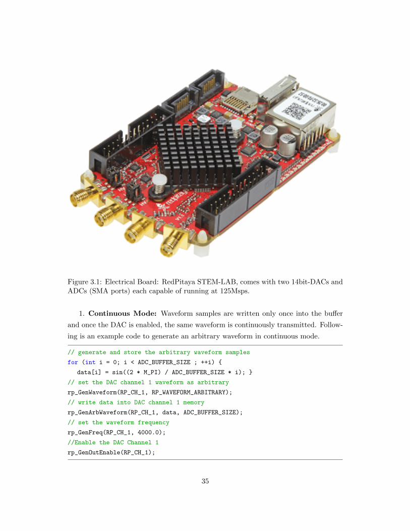
Figure 3.1: Electrical Board: RedPitaya STEM-LAB, comes with two 14bit-DACs andADCs (SMA ports) each capable of running at 125Msps.
1. Continuous Mode: Waveform samples are written only once into the buffer
and once the DAC is enabled, the same waveform is continuously transmitted. Follow-
ing is an example code to generate an arbitrary waveform in continuous mode.
// generate and store the arbitrary waveform samples
for (int i = 0; i < ADC_BUFFER_SIZE ; ++i) {
data[i] = sin((2 * M_PI) / ADC_BUFFER_SIZE * i); }
// set the DAC channel 1 waveform as arbitrary
rp_GenWaveform(RP_CH_1, RP_WAVEFORM_ARBITRARY);
// write data into DAC channel 1 memory
rp_GenArbWaveform(RP_CH_1, data, ADC_BUFFER_SIZE);
// set the waveform frequency
rp_GenFreq(RP_CH_1, 4000.0);
//Enable the DAC Channel 1
rp_GenOutEnable(RP_CH_1);
35
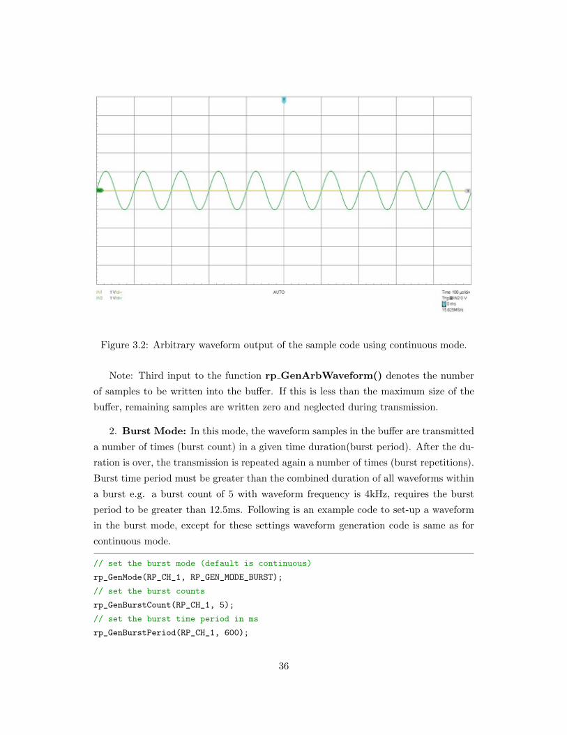
Figure 3.2: Arbitrary waveform output of the sample code using continuous mode.
Note: Third input to the function rp GenArbWaveform() denotes the number
of samples to be written into the buffer. If this is less than the maximum size of the
buffer, remaining samples are written zero and neglected during transmission.
2. Burst Mode: In this mode, the waveform samples in the buffer are transmitted
a number of times (burst count) in a given time duration(burst period). After the du-
ration is over, the transmission is repeated again a number of times (burst repetitions).
Burst time period must be greater than the combined duration of all waveforms within
a burst e.g. a burst count of 5 with waveform frequency is 4kHz, requires the burst
period to be greater than 12.5ms. Following is an example code to set-up a waveform
in the burst mode, except for these settings waveform generation code is same as for
continuous mode.
// set the burst mode (default is continuous)
rp_GenMode(RP_CH_1, RP_GEN_MODE_BURST);
// set the burst counts
rp_GenBurstCount(RP_CH_1, 5);
// set the burst time period in ms
rp_GenBurstPeriod(RP_CH_1, 600);
36
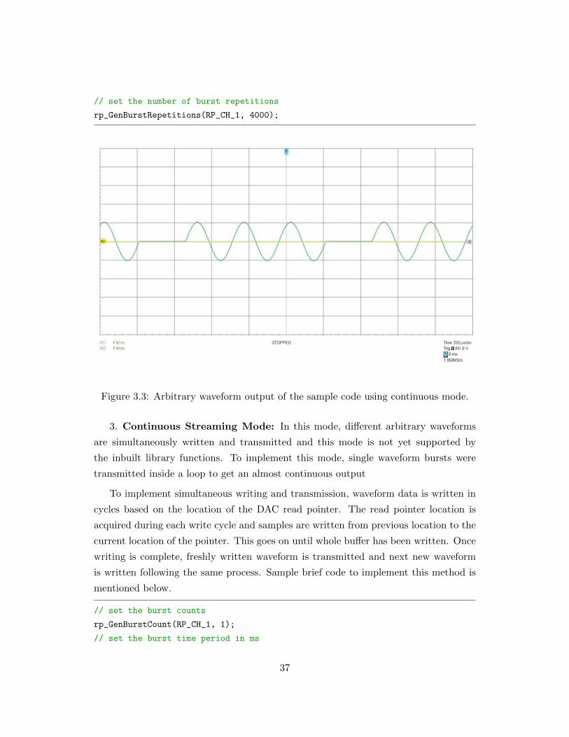
// set the number of burst repetitions
rp_GenBurstRepetitions(RP_CH_1, 4000);
Figure 3.3: Arbitrary waveform output of the sample code using continuous mode.
3. Continuous Streaming Mode: In this mode, different arbitrary waveforms
are simultaneously written and transmitted and this mode is not yet supported by
the inbuilt library functions. To implement this mode, single waveform bursts were
transmitted inside a loop to get an almost continuous output
To implement simultaneous writing and transmission, waveform data is written in
cycles based on the location of the DAC read pointer. The read pointer location is
acquired during each write cycle and samples are written from previous location to the
current location of the pointer. This goes on until whole buffer has been written. Once
writing is complete, freshly written waveform is transmitted and next new waveform
is written following the same process. Sample brief code to implement this method is
mentioned below.
// set the burst counts
rp_GenBurstCount(RP_CH_1, 1);
// set the burst time period in ms
37

rp_GenBurstPeriod(RP_CH_1, 16384/1.93);
// set the number of burst repetitions
rp_GenBurstRepetitions(RP_CH_1, 1)
for(frm_num=0; frm_num<N_FRAMES; frm_num++){
// get the read pointer once to update from zero
rp_GenGetReadPointer(&curr_pos, RP_CH_2);
// prepare the waveform (could be any other function)
for(i = 0; i < ADC_BUFFER_SIZE; i++)
buff[i] = sin((2*M_PI)/(ADC_BUFFER_SIZE)*i);
// write the data in cycles
for(prev_pos=0; prev_pos<ADC_BUFFER_SIZE;){
rp_GenGetReadPointer(&curr_pos, RP_CH_2);
// check whether transmission stops (curr_pos will be zero)
curr_pos = ((curr_pos==0)?(ADC_BUFFER_SIZE):curr_pos);
// write from prev_pos to current position
for(;prev_pos<curr_pos;prev_pos++)
dac_add[prev_pos] =
cnv_volt_to_count(((frm_num%20)+5/25)*buff[prev_pos]));
}
rp_GenOutEnable(RP_CH_2);
}
Sampling Rate Limitation: Reliable transmission in streaming mode is only possi-
ble when the speed at which the samples are written is greater than rate at which they
are transmitted, else they will be overwritten even before they are transmitted. The
fastest possible write time for a full size waveform is around 5.2-5.3ms, figure 3.4. This
limitation restricts the potential utilization of sampling rate of the board for continuous
streaming mode. The highest possible DAC sampling rate that can be used for stream-
ing is 16384/5.3ms = 3.1Msps. For the current implementation, DAC sampling rate
was set a bit lower at 1.93Msps to match with the receiver (see continuous acquisition
mode).
When writing speed is considerably faster than the operating sampling rate, the
number of samples written in the last write cycle, before the next transmission is
enabled, is very small. Thus the delay between adjacent waveforms is almost negligible
compared to the waveform duration and almost continuous waveform streaming is
achieved.
38
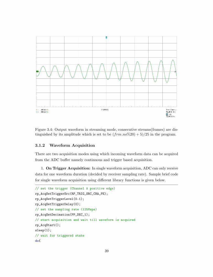
Figure 3.4: Output waveform in streaming mode, consecutive streams(frames) are dis-tinguished by its amplitude which is set to be (frm no%20) + 5)/25 in the program.
3.1.2 Waveform Acquisition
There are two acquisition modes using which incoming waveform data can be acquired
from the ADC buffer namely continuous and trigger based acquisition.
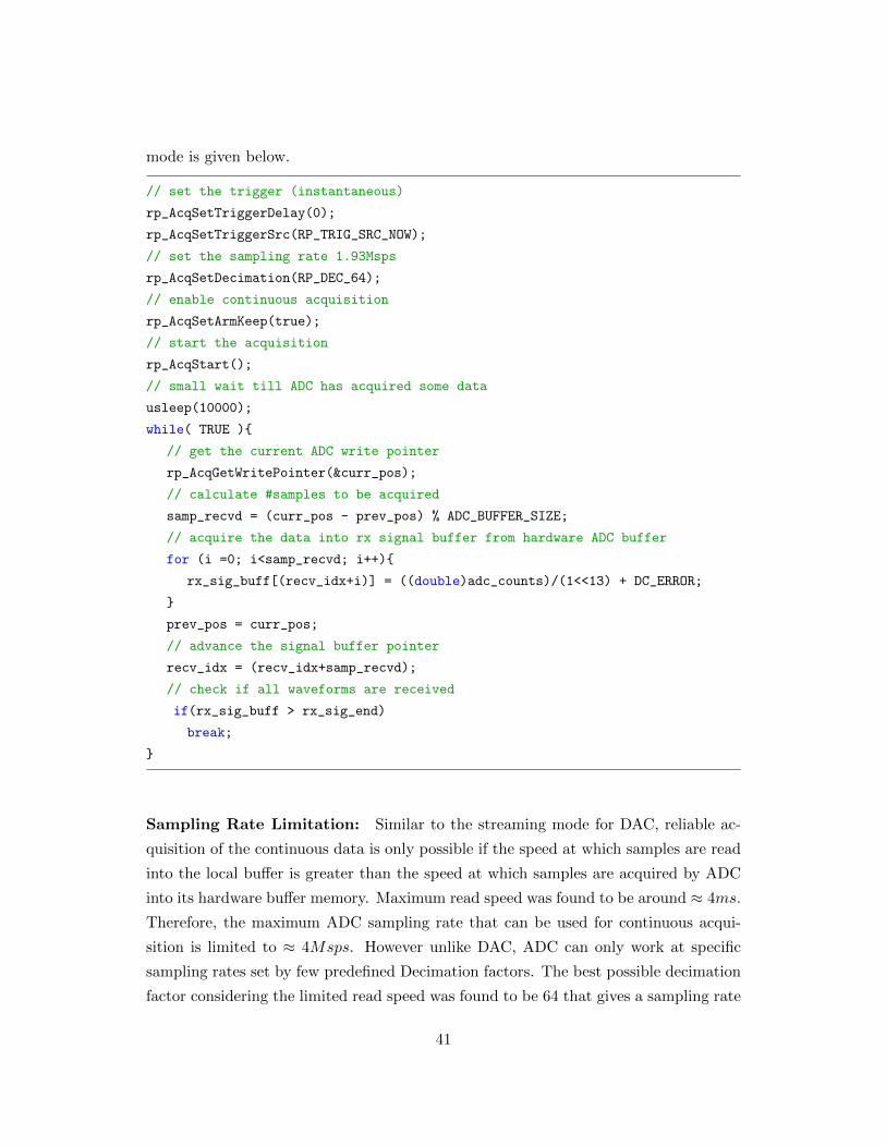
1. On Trigger Acquisition: In single waveform acquisition, ADC can only receive
data for one waveform duration (decided by receiver sampling rate). Sample brief code
for single waveform acquisition using different library functions is given below.
// set the trigger (Channel A positive edge)
rp_AcqSetTriggerSrc(RP_TRIG_SRC_CHA_PE);
rp_AcqSetTriggerLevel(0.1);
rp_AcqSetTriggerDelay(0);
// set the sampling rate (125Msps)
rp_AcqSetDecimation(PP_DEC_1);
// start acquisition and wait till waveform is acquired
rp_AcqStart();
sleep(1);
// wait for triggered state
do{
39
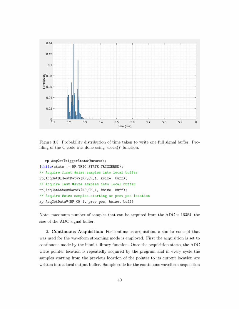
Figure 3.5: Probability distribution of time taken to write one full signal buffer. Pro-filing of the C code was done using ’clock()’ function.
rp_AcqGetTriggerState(&state);
}while(state != RP_TRIG_STATE_TRIGGERED);
// Acquire first #size samples into local buffer
rp_AcqGetOldestDataV(RP_CH_1, &size, buff);
// Acquire last #size samples into local buffer
rp_AcqGetLatestDataV(RP_CH_1, &size, buff);
// Acquire #size samples starting ar prev_pos location
rp_AcqGetDataV(RP_CH_1, prev_pos, &size, buff)
Note: maximum number of samples that can be acquired from the ADC is 16384, the
size of the ADC signal buffer.
2. Continuous Acquisition: For continuous acquisition, a similar concept that
was used for the waveform streaming mode is employed. First the acquisition is set to
continuous mode by the inbuilt library function. Once the acquisition starts, the ADC
write pointer location is repeatedly acquired by the program and in every cycle the
samples starting from the previous location of the pointer to its current location are
written into a local output buffer. Sample code for the continuous waveform acquisition
40
mode is given below.
// set the trigger (instantaneous)
rp_AcqSetTriggerDelay(0);
rp_AcqSetTriggerSrc(RP_TRIG_SRC_NOW);
// set the sampling rate 1.93Msps
rp_AcqSetDecimation(RP_DEC_64);
// enable continuous acquisition
rp_AcqSetArmKeep(true);
// start the acquisition
rp_AcqStart();
// small wait till ADC has acquired some data
usleep(10000);
while( TRUE ){
// get the current ADC write pointer
rp_AcqGetWritePointer(&curr_pos);
// calculate #samples to be acquired
samp_recvd = (curr_pos - prev_pos) % ADC_BUFFER_SIZE;
// acquire the data into rx signal buffer from hardware ADC buffer
for (i =0; i<samp_recvd; i++){
rx_sig_buff[(recv_idx+i)] = ((double)adc_counts)/(1<<13) + DC_ERROR;
}
prev_pos = curr_pos;
// advance the signal buffer pointer
recv_idx = (recv_idx+samp_recvd);
// check if all waveforms are received
if(rx_sig_buff > rx_sig_end)
break;
}
Sampling Rate Limitation: Similar to the streaming mode for DAC, reliable ac-
quisition of the continuous data is only possible if the speed at which samples are read
into the local buffer is greater than the speed at which samples are acquired by ADC
into its hardware buffer memory. Maximum read speed was found to be around ≈ 4ms.
Therefore, the maximum ADC sampling rate that can be used for continuous acqui-
sition is limited to ≈ 4Msps. However unlike DAC, ADC can only work at specific
sampling rates set by few predefined Decimation factors. The best possible decimation
factor considering the limited read speed was found to be 64 that gives a sampling rate
41
of 1.93Msps. For simplicity in the implementation sampling rate of both ADC and
DAC has been kept exactly the same.
3.2 Optical Sources
There are two different optical sources were used for experiments done in this project.
1. 20mW 520nm Laser with Direct Modulation:
This laser from LasersCom is fabricated on a single semiconductor substrate in
Fabry-Perot cavity and does not involve any frequency doubler to emit green
light @520nm. Detailed specification can be found on the manufacturer’s website
(LDI-520-FP-20). Direct modulation was used for generating intensity modulated
optical signal.
2. 1W 532nm with External Modulation:
This laser from CNI (Changchun New Industries) uses an infra-red source at
1064nm and a frequency doubler to generate 532nm green light. Laser has an
external driver to supply the power. This high power laser was used with two
different external modulators EOM and AOM (explained later in the chapter) for
generating the intensity modulated optical signal.
3.3 Optical Modulators
1. Direct Modulation: For optical intensity modulation there are two methods,
direct and indirect modulation. In direct modulation, the electrical signal is directly
applied to the optical source and intensity modulation is achieved. For lasers, the
intensity is proportional to the drive current, thus by changing the drive current direct
modulation can be achieved. For changing the drive current, a simple laser driver
circuit was designed which will take input signal the RedPitaya board and generate a
modulation current. Details of this circuit are presented later.
2. Indirect Modulation: Indirect or external modulation is more complex method
and requires use of special materials which will alter the propagation of light when
some electrical signal is applied to them. Two such modulation methods that are being
used under this project.
42
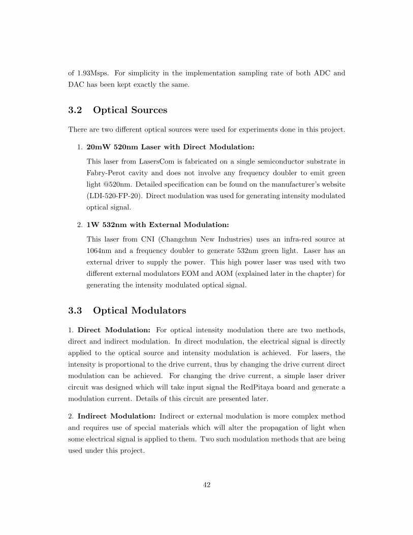
(a) Acousto-Optic Modulation: This method uses an acousto-optic crystal, also
called Bragg Cell, to modulate the optical signal. The cell contains a piezoelectric
transducer which upon application of high frequency RF signal sends an acoustic wave
through crystal that creates diffraction gratings within the crystal. When light goes
through the cell, it gets diffracted depending on when a signal is applied to the crystal
or not and diffraction causes change in the intensity. Light diffraction by a Bragg cell
in shown in figure 3.7. The AOM used in the project responded much better only to
the on-off type of signals, hence only used for PPM experiments.
Figure 3.6: Diffraction of light beam causing change in the intensity when a soundwave travels in an acousto-optic crystal [6].
The AOM used for this project comes with a driver module that generates the
RF signal to actuate the transducer. However, the input signal to the driver module
required more voltage than the Redpitaya Board could supply. Therefore, a simple
op-amp based pre-amplifier circuit in conjunction with a BJT (for high current) was
used. Circuit details are presented later.
43
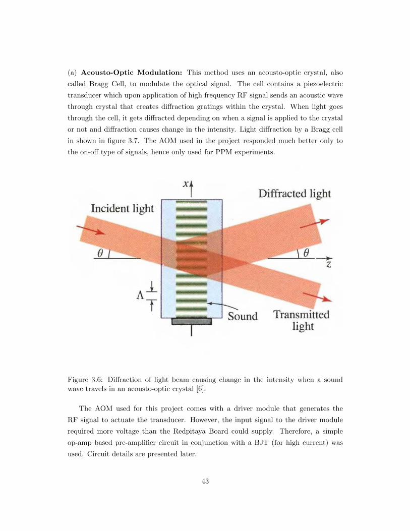
(b) Electro-Optic Modulation: This method uses an electro-optic crystal, also
called Pockel’s Cell, which exhibits birefringence upon application of an electric signal.
There are two ways to modulate the light using an electro-optic crystal as mentioned
below.
i. Variable Waveplate Between two polarisers: The crystal acts as a variable
wave plate for a light beam having polarization states along both the ordinary and
the extraordinary axes of the crystal. This changes the polarization of the output
beam from the crystal depending on the applied voltage to the crystal. Thus, by
using two aligned or crossed polarisers one each at the input and output, intensity
modulation can be achieved. The EOM Arrangement used for the experiment is
shown in Figure 3.8. There is an extra Quarter Wave Plate used in the arrangement
to shift the operating point of the modulator (equivalent to a DC bias as it adds a
fixed pre-retardation before the crystal.
Figure 3.7: Intensity Modulation using an electro-optic crystal between two alignedpolarisers.
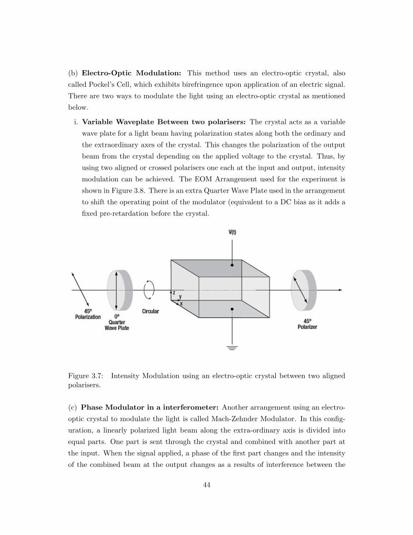
(c) Phase Modulator in a interferometer: Another arrangement using an electro-
optic crystal to modulate the light is called Mach-Zehnder Modulator. In this config-
uration, a linearly polarized light beam along the extra-ordinary axis is divided into
equal parts. One part is sent through the crystal and combined with another part at
the input. When the signal applied, a phase of the first part changes and the intensity
of the combined beam at the output changes as a results of interference between the
44
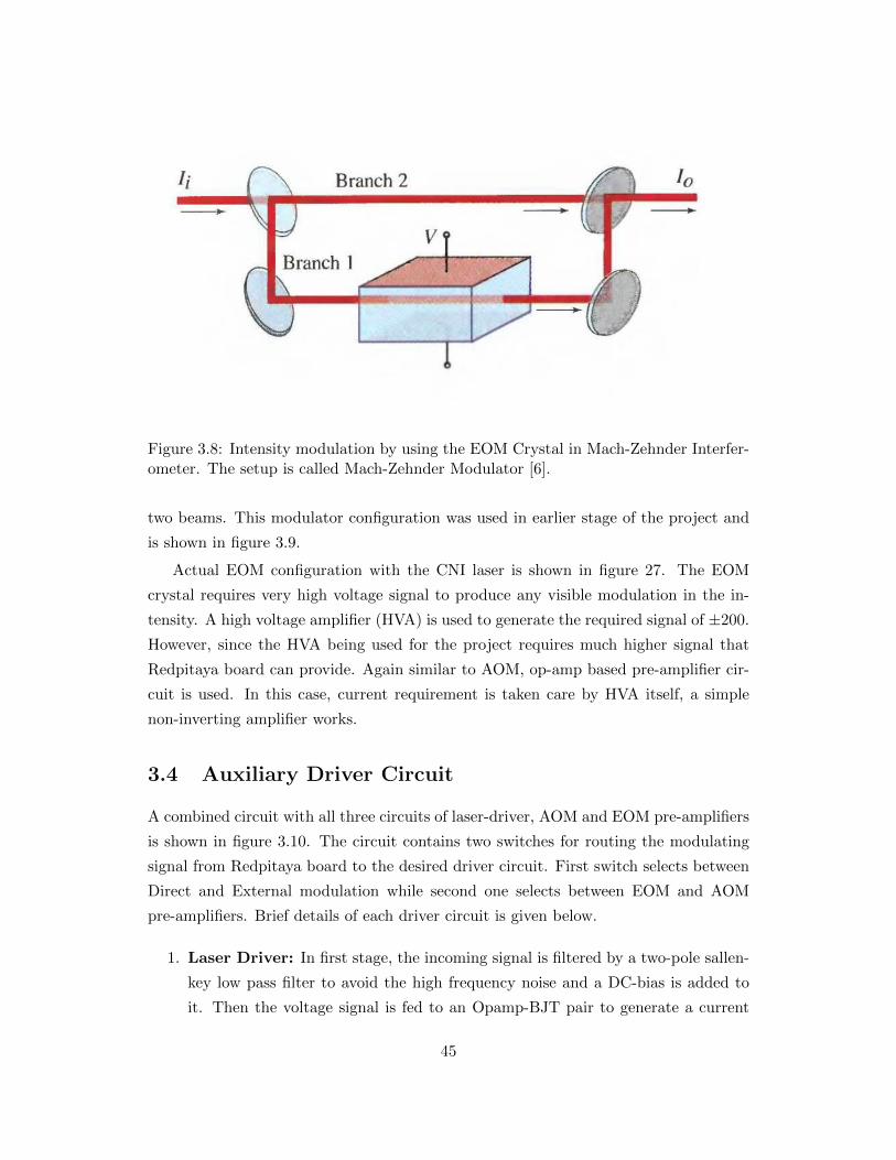
Figure 3.8: Intensity modulation by using the EOM Crystal in Mach-Zehnder Interfer-ometer. The setup is called Mach-Zehnder Modulator [6].
two beams. This modulator configuration was used in earlier stage of the project and
is shown in figure 3.9.
Actual EOM configuration with the CNI laser is shown in figure 27. The EOM
crystal requires very high voltage signal to produce any visible modulation in the in-
tensity. A high voltage amplifier (HVA) is used to generate the required signal of ±200.
However, since the HVA being used for the project requires much higher signal that
Redpitaya board can provide. Again similar to AOM, op-amp based pre-amplifier cir-
cuit is used. In this case, current requirement is taken care by HVA itself, a simple
non-inverting amplifier works.
3.4 Auxiliary Driver Circuit
A combined circuit with all three circuits of laser-driver, AOM and EOM pre-amplifiers
is shown in figure 3.10. The circuit contains two switches for routing the modulating
signal from Redpitaya board to the desired driver circuit. First switch selects between
Direct and External modulation while second one selects between EOM and AOM
pre-amplifiers. Brief details of each driver circuit is given below.
1. Laser Driver: In first stage, the incoming signal is filtered by a two-pole sallen-
key low pass filter to avoid the high frequency noise and a DC-bias is added to
it. Then the voltage signal is fed to an Opamp-BJT pair to generate a current
45
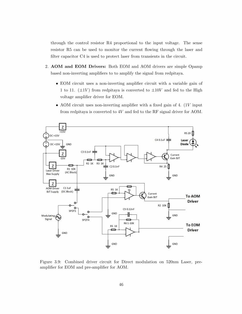
through the control resistor R4 proportional to the input voltage. The sense
resistor R5 can be used to monitor the current flowing through the laser and
filter capacitor C4 is used to protect laser from transients in the circuit.
2. AOM and EOM Drivers: Both EOM and AOM drivers are simple Opamp
based non-inverting amplifiers to to amplify the signal from redpitaya.
• EOM circuit uses a non-inverting amplifier circuit with a variable gain of
1 to 11. (±1V ) from redpitaya is converted to ±10V and fed to the High
voltage amplifier driver for EOM.
• AOM circuit uses non-inverting amplifier with a fixed gain of 4. (1V input
from redpitaya is converted to 4V and fed to the RF signal driver for AOM.
Figure 3.9: Combined driver circuit for Direct modulation on 520nm Laser, pre-amplifier for EOM and pre-amplifier for AOM.
46
3.5 Optical Detectors
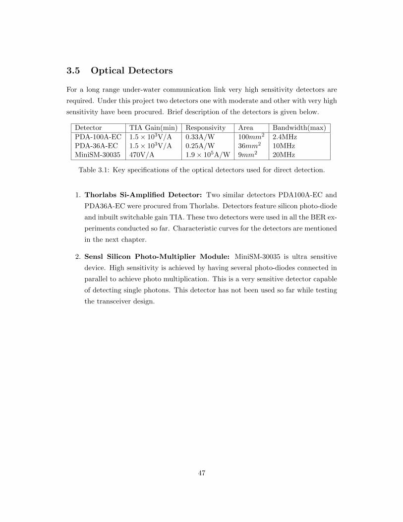
For a long range under-water communication link very high sensitivity detectors are
required. Under this project two detectors one with moderate and other with very high
sensitivity have been procured. Brief description of the detectors is given below.
Detector TIA Gain(min) Responsivity Area Bandwidth(max)
PDA-100A-EC 1.5× 10³V/A 0.33A/W 100mm2 2.4MHzPDA-36A-EC 1.5× 10³V/A 0.25A/W 36mm2 10MHzMiniSM-30035 470V/A 1.9× 10⁵A/W 9mm2 20MHz
Table 3.1: Key specifications of the optical detectors used for direct detection.
1. Thorlabs Si-Amplified Detector: Two similar detectors PDA100A-EC and
PDA36A-EC were procured from Thorlabs. Detectors feature silicon photo-diode
and inbuilt switchable gain TIA. These two detectors were used in all the BER ex-
periments conducted so far. Characteristic curves for the detectors are mentioned
in the next chapter.
2. Sensl Silicon Photo-Multiplier Module: MiniSM-30035 is ultra sensitive
device. High sensitivity is achieved by having several photo-diodes connected in
parallel to achieve photo multiplication. This is a very sensitive detector capable
of detecting single photons. This detector has not been used so far while testing
the transceiver design.
47
Chapter 4
Transceiver Software
This chapter describes the details of the software programs and algorithms used for
implementing the PPM and OFDM transceivers. Major part of this chapter is devoted
to the receiver synchronization without which continuously streamed signal can not be
detected. For continuous synchronization, waveforms are sent using a predefined frame
structure. Frame formation is discussed after synchronization. In the end, stepwise
execution of both the receiver and the transmitter programs is explained.
4.1 PPM Synchronization
Synchronization for PPM is done by sending a pn-sequence at the start of the ev-
ery waveform (or frame). PN-sequence, also called m-sequence, has very good auto-
correlation properties. Any shifted version of the sequence has very low correlation
with the sequence.
1. Sync Sequence Generation: A 32-length pseudo random binary sequence was
used as the desired sync sequence. For maintaining the better correlation proper-
ties across the frame, the PRBS11 pattern was used for binary data and PRBS7
pattern was used for the sync sequence. Furthermore, a different modulation for-
mat, OOK-NRZ, was used for sending the sync sequence while binary data was
sent using PPM format.
2. Detection of Sync Sequence: For sequential detection of received frames, a
sliding window correlation between the received sequence and the already-known
PN-sequence is calculated. Synchronization completes as soon as the correlation
48
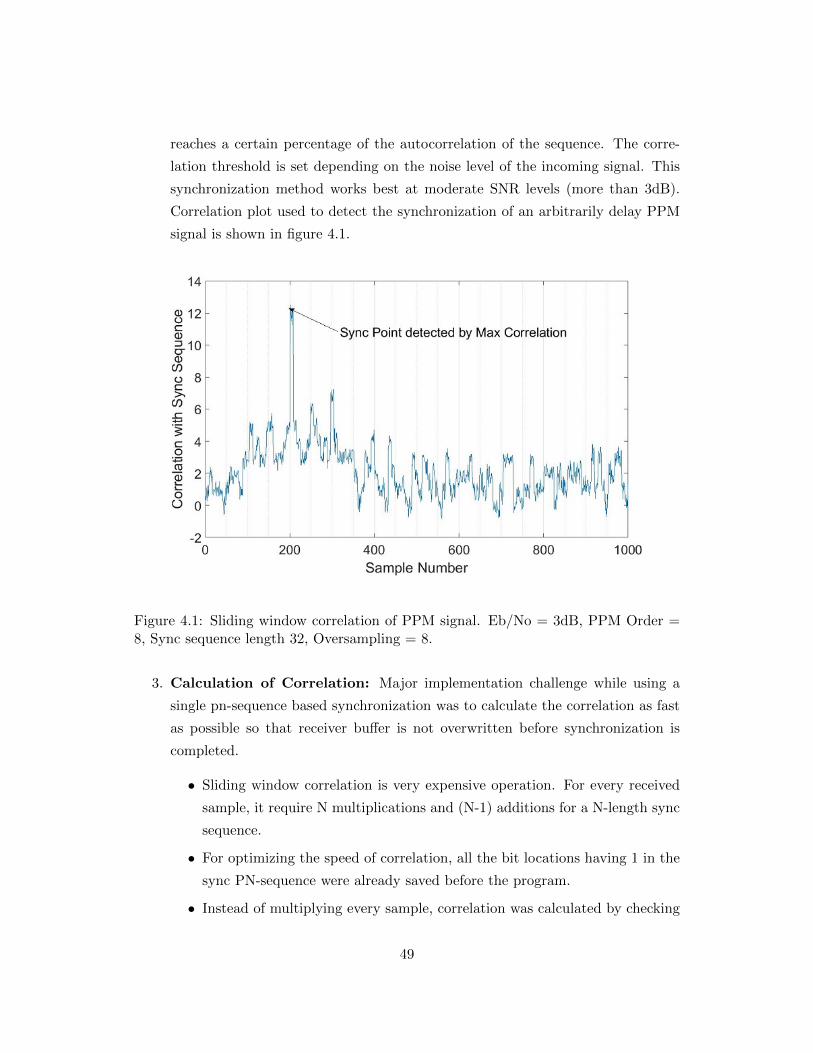
reaches a certain percentage of the autocorrelation of the sequence. The corre-
lation threshold is set depending on the noise level of the incoming signal. This
synchronization method works best at moderate SNR levels (more than 3dB).
Correlation plot used to detect the synchronization of an arbitrarily delay PPM
signal is shown in figure 4.1.
Figure 4.1: Sliding window correlation of PPM signal. Eb/No = 3dB, PPM Order =8, Sync sequence length 32, Oversampling = 8.
3. Calculation of Correlation: Major implementation challenge while using a
single pn-sequence based synchronization was to calculate the correlation as fast
as possible so that receiver buffer is not overwritten before synchronization is
completed.
• Sliding window correlation is very expensive operation. For every received
sample, it require N multiplications and (N-1) additions for a N-length sync
sequence.
• For optimizing the speed of correlation, all the bit locations having 1 in the
sync PN-sequence were already saved before the program.
• Instead of multiplying every sample, correlation was calculated by checking
49
the received sample values only at those bit locations having ’1’.
• Simplified expression for sliding window correlation between an N length
sync sequence sn andK times oversampled received sequence rn at ith sample
position is given below.
Corr(i) =
N−1∑n=0
snr(n∗K+i) =
N−1∑n=0,n6=m
(∀m: sm=0)
(r(n∗K+i) > th)
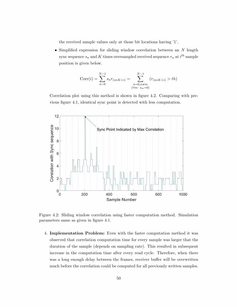
Correlation plot using this method is shown in figure 4.2. Comparing with pre-
vious figure 4.1, identical sync point is detected with less computation.
Figure 4.2: Sliding window correlation using faster computation method. Simulationparameters same as given in figure 4.1.
4. Implementation Problem: Even with the faster computation method it was
observed that correlation computation time for every sample was larger that the
duration of the sample (depends on sampling rate). This resulted in subsequent
increase in the computation time after every read cycle. Therefore, when there
was a long enough delay between the frames, receiver buffer will be overwritten
much before the correlation could be computed for all previously written samples.
50

This limits the maximum amount of delay that that can be handled by this
method.
5. Double PN-Sequence Synchronization: Alternate method to make the com-
putation of correlation faster is to use a pair of identical pn-sequences instead of
a single sequence and use their correlation as the deciding parameter. Whenever
this sequence will appear in the received signal, correlation will have a maximum.
Two advantages of double pn-sequence are given below:
(a) Using two sequences requires no knowledge of sync sequence at the receiver.
Correlation is computed from the received sequence itself as shown below.
Corr(i) =
N−1∑n=0
r(n∗K+i)r(n∗K+i+N)
(b) Full computation of correlation is required only once for the first sample.
For next samples, correlation is simply updated using its previous value and
requires only two multiplications and two additions. This method has not
been implemented currently but is preferred method for faster processing.
Corr(i) = Corr(i− 1)− r(i−1)r(i−1+N) + r((N−1)K+i)r((N−1)K+i+N)
6. Length of the Sequence: Length of the PN-sequence was decided as 32 using
trial and error method. A larger PN sequence gives better synchronization but
requires more computation, while a shorter sequence does not have a very high
correlation hence more prone to false synchronizations.
7. Effect of oversampling: Oversampling has two effects on correlation value.
It increase the correlation value K times if sequence is used as it is. It also
increases the duration (number of samples) over which the correlation will retain
its maxima. Both these properties help in minimizing the synchronization error.
Overall effect of oversampling is summarized below.
• Larger the value of the correlation of sync sequence compared to the corre-
lation of noise, more robust will be the synchronization at low SNR values.
• Larger duration over which true maximum is present, probability of all max-
imum having a value less than correlation threshold reduces.
51
• However, as the oversampling factor increases, the correlation length in-
creases and more computation is required.
• Since the computation is already expensive with a single pn-sequence, only
the second property was utilized. For calculation of the correlation, received
sequence was fully down-sampled.
4.2 OFDM Synchronization
The OFDM synchronization algorithm uses the anti-symmetry property of the Fourier
Transform to generate a special synchronization sequence with very good correlation
properties. The cross-correlation between the two halves of the sync sequence is very
strong and equal to the half of the total symbol power (or auto-correlation of either
half of sequence). This sync sequence is added at the start of the frame in form of an
extra OFDM symbol. Overall synchronization for OFDM is done in two steps rough
frame synchronization and sync error correction.
1. Sync Sequence Generation: For generating the anti symmetric symbol, ran-
dom QAM data was placed only at the odd sub-carrier of the OFDM symbol.
A typical anti-symmetric OFDM sequence is shown in figure 2.5 in second chap-
ter while discussing ACO-OFDM. First and second halves of the sequence are
identical except for a minus sign.
2. Detection of Sync Sequence: Whenever the sync sequence appears in the
received waveform, the ratio of cross-correlation and auto-correlation attains a
maximum value and retains it as long as correlation window (half of FFT Size)
remains within the sync symbol. If the oversampling is K times and length of
cyclic prefix is CP, the maximum will be retained over a number of (K*CP+1)
samples from the start of the sync symbol.
For detecting the exact sync point, window minimum of the correlation ratios
over (K*CP+1) samples is taken. As shown in the window minimum plot in
figure 4.3, a local maximum occurs exactly at the start of the synchronization
sequence.
3. Computation of Correlation Ratio: Since correlation is computed within
the received received sequence, computation can be done progressively using the
previous value correlation values, similar to double PN-sequence synchronization
52
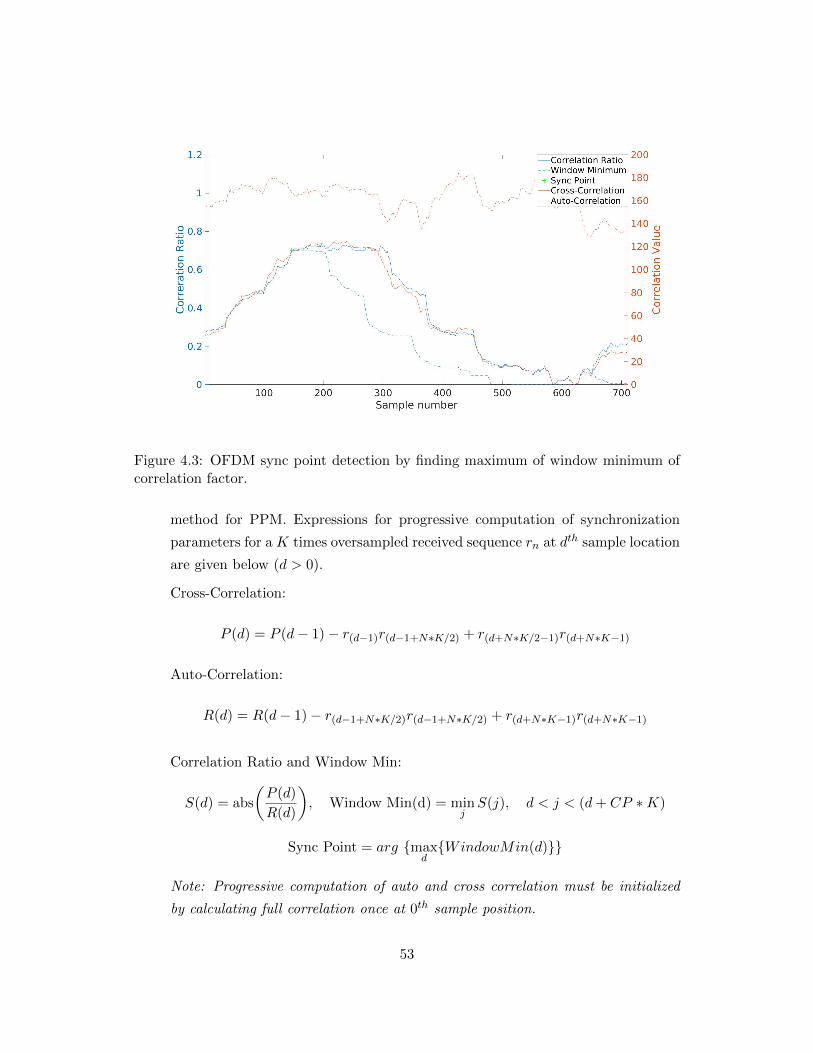
Figure 4.3: OFDM sync point detection by finding maximum of window minimum ofcorrelation factor.
method for PPM. Expressions for progressive computation of synchronization
parameters for a K times oversampled received sequence rn at dth sample location
are given below (d > 0).
Cross-Correlation:
P (d) = P (d− 1)− r(d−1)r(d−1+N∗K/2) + r(d+N∗K/2−1)r(d+N∗K−1)
Auto-Correlation:
R(d) = R(d− 1)− r(d−1+N∗K/2)r(d−1+N∗K/2) + r(d+N∗K−1)r(d+N∗K−1)
Correlation Ratio and Window Min:
S(d) = abs
(P (d)
R(d)
), Window Min(d) = min
jS(j), d < j < (d+ CP ∗K)
Sync Point = arg {maxd{WindowMin(d)}}
Note: Progressive computation of auto and cross correlation must be initialized
by calculating full correlation once at 0th sample position.
53
4. Computation of window minimum: Simplest way to find the window min-
imum for current sample is to save the correlation ratio for a number of future
samples depending on the length of window and find the minimum among them.
However, this method is computationally very expensive, requires (K ∗ CP + 1)
comparisons for every received sample. lllA more efficient algorithm which calcu-
lates the moving window minimum using a multi-sorted array has been used in
the current implementation.
• Algorithm uses a double ended queue of length equal to the (K ∗ CP + 2)
to store the correlation ratios and corresponding sample numbers.
• Double ended queue is data structure to implement a circular buffer in which
data can be inserted and removed from either side. This queue also keeps
track of the front and the back indices of the buffer.
• Algorithm runs in such a way that both the correlation ratio and the sample
number are always stored in an ascending order, starting from front to the
back index of the queue.
• To find the location of window minimum for the current sample, simply the
sample number stored at front index is taken.
Detailed explanation of implementation of window minimum and how it reduces
the computation complexity has been given at [9].
5. Local Maximum of window minimum: Exactly sample at which the local
maximum of window minimum has occurred can be found by keeping track of
the window minimum value as mentioned below.
• For every sample, the current window minimum is compared with the current
maximum of window minimum.
• If the current window minimum is greater, current maximum and corre-
sponding sample number is updated.
• If the current window minimum is smaller, ratio with respect to the current
maximum is calculated. If it is less than a predefined threshold (60% is
used), synchronization stops.
• Once synchronization stops, the current maximum is accepted as the true
local maximum and corresponding sample number is taken as the synchro-
nization point.
54
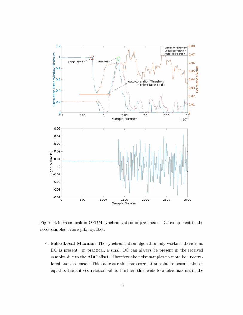
Figure 4.4: False peak in OFDM synchronization in presence of DC component in the
noise samples before pilot symbol.
6. False Local Maxima: The synchronization algorithm only works if there is no
DC is present. In practical, a small DC can always be present in the received
samples due to the ADC offset. Therefore the noise samples no more be uncorre-
lated and zero mean. This can cause the cross-correlation value to become almost
equal to the auto-correlation value. Further, this leads to a false maxima in the
55
window minimum of the correlation ratio even in absence of the pilot signal. One
such situation has been shown in figure 4.4.
7. Rejection of False Maxima: To avoid the detection of these false peaks, a
threshold on the auto correlation value is also set. For verifying a true maximum,
auto-correlation value must be greater than the threshold. Depending on the
amount of DC, the noise level, received signal power threshold must be adjusted
to a optimum.
• A larger threshold limits the low range of the operating SNR. Received signal
power must remain large enough so that auto-correlation of pilot is greater
than threshold.
• A smaller threshold leads to false maximum detection when there no pilot
is present.
8. Effect of oversampling: The effect of oversampling in OFDM is exactly same
as that explained earlier for PPM. Larger the oversampling (smaller the down-
sampling) in the received sequence, smaller will be synchronization error at low
SNR values. Reduction in the synchronization error was studied in simulations.
Plot of mean synchronization error using this sync algorithm vs SNR at different
oversampling factors is shown in figure 4.5.
However, oversampling also increases computational cost, therefore must not be
very high too. Considering the performance trade-offs, the current implementa-
tion uses a 2x downsampling on a 8x oversampled received sequence to get an
effective oversampling of 4 while calculating the correlation.
9. Synchronization Correction: With the above synchronization method, there
are always chances of making synchronization error even at moderate SNR be-
cause a large number of OFDM samples have small amplitudes. To avoid this
problem, estimated sync point is also corrected using a known pilot symbol sent
by the transmitter. For reducing the non-data overhead in the frame, sync se-
quence itself was used as the pilot symbol. Implication of using sync symbol as
the pilot is mentioned in the below mentioned steps for implementing the sync
error correction.
Sync error correction method uses the cyclic prefix for the estimation of the
synchronization error. Steps for correction are mentioned below.
56
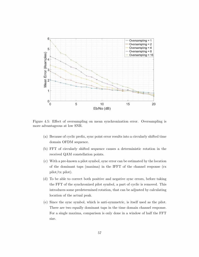
Figure 4.5: Effect of oversampling on mean synchronization error. Oversampling ismore advantageous at low SNR.
(a) Because of cyclic prefix, sync point error results into a circularly shifted time
domain OFDM sequence.
(b) FFT of circularly shifted sequence causes a deterministic rotation in the
received QAM constellation points.
(c) With a pre-known a pilot symbol, sync error can be estimated by the location
of the dominant taps (maxima) in the IFFT of the channel response (rx
pilot/tx pilot).
(d) To be able to correct both positive and negative sync errors, before taking
the FFT of the synchronized pilot symbol, a part of cyclic is removed. This
introduces some predetermined rotation, that can be adjusted by calculating
location of the actual peak.
(e) Since the sync symbol, which is anti-symmetric, is itself used as the pilot.
There are two equally dominant taps in the time domain channel response.
For a single maxima, comparison is only done in a window of half the FFT
size.
57
10. Signal Power Estimation: Demodulation of the QAM symbols is done based
on threshold region of the constellation point. Since the received signal will be
randomly attenuated, the threshold region must be adjusted accordingly for cor-
rect demodulation of the QAM symbols. This requires estimation of channel
attenuation. Channel attenuation is estimated by measuring the power of dom-
inant taps in the time domain channel response. By dividing the expected pilot
power with no attenuation by overall power of all dominant taps will give the
overall attenuation.
Threshold regions for QAM-4 constellation is simply the 4 quadrants of the real
and imaginary plane. Hence, estimation is required only higher order QAM
constellations. This estimation was also be used for setting the auto-correlation
threshold for rejection of false peaks.
4.3 Frame Structure
The modulated signal is transmitted using a predefined structure in order to carry other
non-data overhead in regular intervals. Non-data overhead may involve control infor-
mation, synchronization information, pilot symbols etc. In the current implementation
only two non-data overheads are being used for both PPM and OFDM. Therefore,
there are three parts in the frame structure as mentioned below:
1. Sync sequence - Required for frame synchronization. For OFDM this sequence
also acts as the pilot symbol which is used for synchronization correction and
signal level estimation.
2. Frame Number - Required for BER evaluation in streaming mode when all
frames carry different binary data. During demodulation, there may cases when
few random frames are missed or incorrectly synchronized. In these caase to
evaluate the BER correctly, receiver must know which frame number is received.
Therefore, a frame number is attached to every frame right after the synchroniza-
tion sequence is placed.
Since the whole BER evaluation relies on the accuracy of the frame numbers, the
frame numbers must be error codded so that even when data has some error, the
frame number can be correctly identified for meaningful data comparison. How-
ever, since the error-coding has not been implemented yet, the BER evaluation
58
was not possible or less reliable at low SNR values. Therefore, in the BER exper-
iments, signal transmission was tested in both continuous and streaming modes
to further emphasize this issue.
3. Binary Information - Last remaining portion of the frame is used for sending
the binary information (data payload).
Actually, the frame number and binary data are combined together and then
combined binary data is modulated to get the overall PPM/OFDM Signal.
Frame Length: For optimum data transmission in streaming mode, frame length
was chosen equal to the size of the hardware buffer for the DAC i.e. 16384 samples.
This choice allows almost continuous data transmission in streaming mode as explained
in chapter 4. .
Oversampling: The DAC output from Redpitaya board has a finite rise time and
requires the each written sample to hold for atleast a few sample duration before
any new value can be written. In order to get a ringing free output from DAC, an
oversampling factor of 8 was used while writing the samples into the DAC Memory. For
implementing the oversampling, simplest rectangular pulse was used i.e. each sample
was simply duplicated by the oversampling factor. With this much oversampling, the
effective number of samples in a frame were reduced to 16384/8 = 2048.
PPM Frame:
• For PPM, a 32-length NRZ-OOK modulated sequence was used for synchroniza-
tion accounting.
• Remaining part of the frame (2016 samples) were used to transmit PPM modu-
lated signal carrying the frame number bits and information bits.
• The number of PPM symbols per frame depends on the PPM order and remaining
samples in the frame i.e. no of PPM symbols = (2048-32)/L, where L is the PPM
order.
OFDM Frame:
• For OFDM, the frame structure was based on the choice of FFT Size. For faster
computation, small FFT size of 64 was chosen.
59
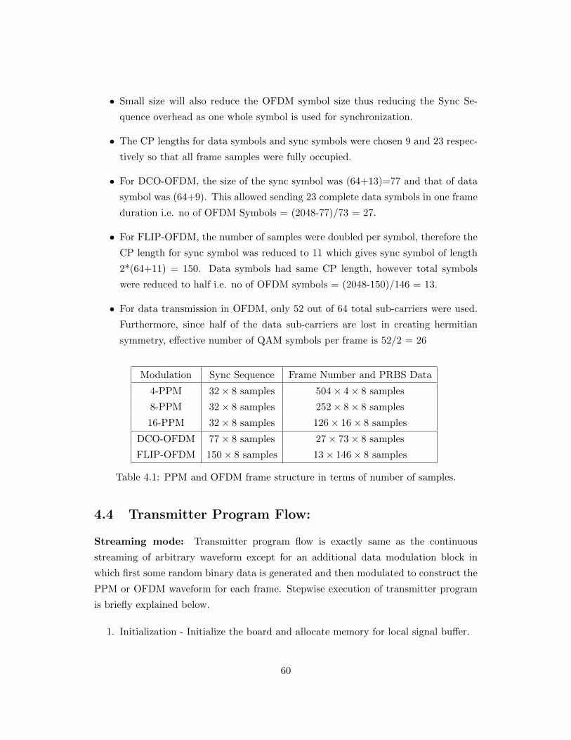
• Small size will also reduce the OFDM symbol size thus reducing the Sync Se-
quence overhead as one whole symbol is used for synchronization.
• The CP lengths for data symbols and sync symbols were chosen 9 and 23 respec-
tively so that all frame samples were fully occupied.
• For DCO-OFDM, the size of the sync symbol was (64+13)=77 and that of data
symbol was (64+9). This allowed sending 23 complete data symbols in one frame
duration i.e. no of OFDM Symbols = (2048-77)/73 = 27.
• For FLIP-OFDM, the number of samples were doubled per symbol, therefore the
CP length for sync symbol was reduced to 11 which gives sync symbol of length
2*(64+11) = 150. Data symbols had same CP length, however total symbols
were reduced to half i.e. no of OFDM symbols = (2048-150)/146 = 13.
• For data transmission in OFDM, only 52 out of 64 total sub-carriers were used.
Furthermore, since half of the data sub-carriers are lost in creating hermitian
symmetry, effective number of QAM symbols per frame is 52/2 = 26
Modulation Sync Sequence Frame Number and PRBS Data
4-PPM 32× 8 samples 504× 4× 8 samples
8-PPM 32× 8 samples 252× 8× 8 samples
16-PPM 32× 8 samples 126× 16× 8 samples
DCO-OFDM 77× 8 samples 27× 73× 8 samples
FLIP-OFDM 150× 8 samples 13× 146× 8 samples
Table 4.1: PPM and OFDM frame structure in terms of number of samples.
4.4 Transmitter Program Flow:
Streaming mode: Transmitter program flow is exactly same as the continuous
streaming of arbitrary waveform except for an additional data modulation block in
which first some random binary data is generated and then modulated to construct the
PPM or OFDM waveform for each frame. Stepwise execution of transmitter program
is briefly explained below.
1. Initialization - Initialize the board and allocate memory for local signal buffer.
60
2. DAC configuration - Set the transmission mode, Sampling rate, amplitude, offset.
Set the DAC channel and acquire its hardware buffer address.
3. Sync Symbol Generation - Generate the sync sequence and store at the head of
transmit signal buffer. This sequence is same for all frames.
4. Continuous Frame Transmission Loop - Main part of program where newly writ-
ten PPM/OFDM frames are streamed.
(a) Get the location of DAC read pointer
(b) Prepare the Transmit Signal
i. generate frame number and PRBS binary data
ii. generate the PPM/OFDM signal
(c) Write the PPM/OFDM signal into the DAC Buffer
i. reset the write pointer to the start
ii. get the current read pointer location
iii. convert the real signal into DAC counts and write it into the DAC buffer
till the current read pointer location. Update the write pointer.
iv. continue from (i) until write pointer reaches the end of the buffer
(d) Transmit the newly written frame and increment frame count.
(e) Continue from (a) until all frames are transmitted
Continuous mode: The program execution is quite similar to the streaming mode
except that the frame data is written only into the buffer and the same data is contin-
uously transmitted repeatedly till the time desired number of frames are transmitted.
This mode was much simpler to implement and test as can be seen in continuous mode
transmission in Chapter 4.
4.5 Receiver Program Flow
Streaming Mode: Receiver program flow is same as the continuous waveform ac-
quisition of arbitrary waveform except for two extra blocks. One signal demodulation
block, which synchronizes and demodulates the signal and stores the binary data, is
added right after the new samples is acquired. Another independent BER evaluation
61
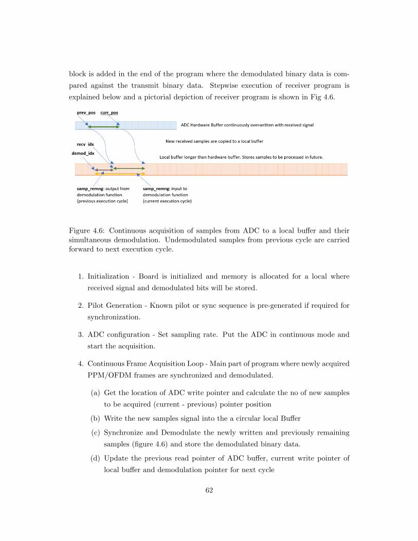
block is added in the end of the program where the demodulated binary data is com-
pared against the transmit binary data. Stepwise execution of receiver program is
explained below and a pictorial depiction of receiver program is shown in Fig 4.6.
Figure 4.6: Continuous acquisition of samples from ADC to a local buffer and theirsimultaneous demodulation. Undemodulated samples from previous cycle are carriedforward to next execution cycle.
1. Initialization - Board is initialized and memory is allocated for a local where
received signal and demodulated bits will be stored.
2. Pilot Generation - Known pilot or sync sequence is pre-generated if required for
synchronization.
3. ADC configuration - Set sampling rate. Put the ADC in continuous mode and
start the acquisition.
4. Continuous Frame Acquisition Loop - Main part of program where newly acquired
PPM/OFDM frames are synchronized and demodulated.
(a) Get the location of ADC write pointer and calculate the no of new samples
to be acquired (current - previous) pointer position
(b) Write the new samples signal into the a circular local Buffer
(c) Synchronize and Demodulate the newly written and previously remaining
samples (figure 4.6) and store the demodulated binary data.
(d) Update the previous read pointer of ADC buffer, current write pointer of
local buffer and demodulation pointer for next cycle
62
(e) Continue until all frames are demodulated or specified time limit is reached
(in case of synchronization fails and no frame is demodulated).
Continuous Mode: Acquisition in continuous mode is exactly as that in the stream-
ing mode except that the synchronization is done only for the first frame. This is be-
cause all frames are transmitted without any delay between them, all frame boundaries
can be determined just by synchronizing the first frame.
4.5.1 Demodulation Program Flow
Synchronization and demodulation block is the most complex part of the overall transceiver
design since random number of samples acquired by the ADC in every read cycle and
these samples could belong to any part of the frame. For deciding what should be
done for received samples at any point of time, flags are used to indicate whether syn-
chronization or demodulation should be run. Stepwise execution of the demodulation
function is explained below..
1. Get the demodulation pointer and Number of samples to be demodulated
2. Check if synchronization flag is not set.
(a) Reset the demodulated symbol count and run the synchronization until no
more samples are left or synchronization is complete.
(b) If synchronization is complete, set the synchronization flag and exit synchro-
nization block.
(c) If synchronization is not complete but all samples have been checked for
synchronization, exit the function.
3. Check if synchronization flag is set.
(a) calculate the max no of symbols that can be demodulated from the received
no of samples.
(b) calculate the frame symbol count including the max no of symbols that can
be demodulated
(c) if the count exceeds no of symbols per frame, change the no of symbols to
be demodulated so that count is equal to no of symbols per frame
(d) run the demodulation for no of symbols to be demodulated
63
(e) if frame symbol count is equal to the no of symbols per frame (end of frame),
rerun the demodulation function with remaining unprocessed samples.
4. calculate number of bits received from no of demodulated symbols
5. return the remaining unprocessed samples and no of demodulated bits
4.5.2 BER Evaluation
BER evaluation is the last part of the receiver program and run after the demodulation
is completed. There are two different methods used for evaluation of the BER using
the demodulated binary data for streaming and continuous modes respectively.
1. Frame Number Based (Streaming Mode):
• In this method, BER was evaluated per frame basis only for the valid re-
ceived frames.
• Decision, whether a frame number was valid or not, was taken on the basis
of the frame difference between between two adjacent received frames.
• If the difference was less than 10, the current frame was counted as valid. If
the frame difference was negative or larger than 10, the frame was assumed
to be incorrectly synchronized and hence called invalid and not considered
while evaluating the BER.
• As synchronization error increases effective number of frames considered for
BER evaluation decrease therefore this method does not work properly at
low SNRs.
• If there is a bit flip in the frame number itself (possible at low SNR), even
valid frames could counted as invalid. Therefore, frame numbers must be
error coded.
2. Direct Evaluation (Continuous Mode):
• In this method, all frames are considered for BER evaluation as synchro-
nization is done only once in continuous mode.
• Depending on whether synchronization is correct or not, BER evaluation
could be correct or completely incorrect.
• However, it was observed during the experiments that finding one correctly
synchronized was not difficult even at low SNR values.
64
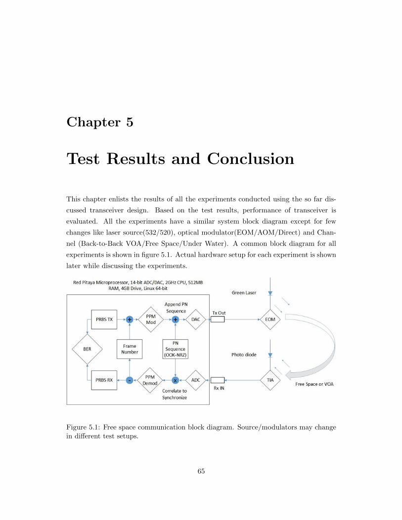
Chapter 5
Test Results and Conclusion
This chapter enlists the results of all the experiments conducted using the so far dis-
cussed transceiver design. Based on the test results, performance of transceiver is
evaluated. All the experiments have a similar system block diagram except for few
changes like laser source(532/520), optical modulator(EOM/AOM/Direct) and Chan-
nel (Back-to-Back VOA/Free Space/Under Water). A common block diagram for all
experiments is shown in figure 5.1. Actual hardware setup for each experiment is shown
later while discussing the experiments.
Figure 5.1: Free space communication block diagram. Source/modulators may changein different test setups.
65
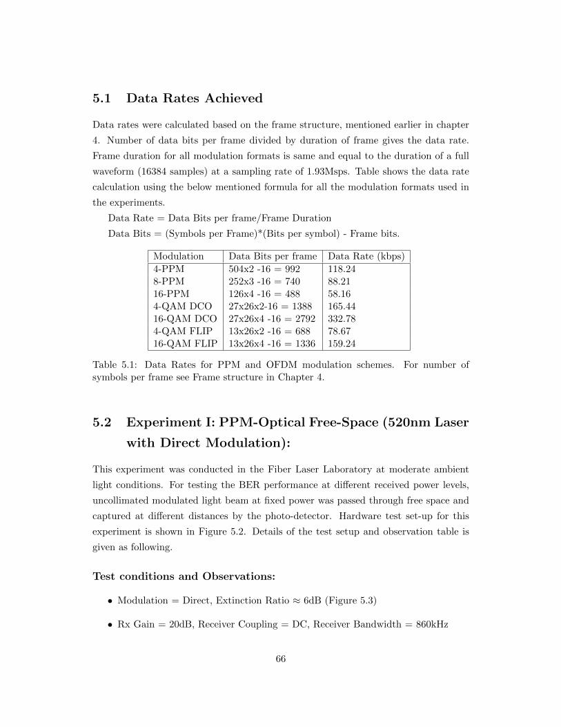
5.1 Data Rates Achieved
Data rates were calculated based on the frame structure, mentioned earlier in chapter
4. Number of data bits per frame divided by duration of frame gives the data rate.
Frame duration for all modulation formats is same and equal to the duration of a full
waveform (16384 samples) at a sampling rate of 1.93Msps. Table shows the data rate
calculation using the below mentioned formula for all the modulation formats used in
the experiments.
Data Rate = Data Bits per frame/Frame Duration
Data Bits = (Symbols per Frame)*(Bits per symbol) - Frame bits.
Modulation Data Bits per frame Data Rate (kbps)
4-PPM 504x2 -16 = 992 118.248-PPM 252x3 -16 = 740 88.2116-PPM 126x4 -16 = 488 58.164-QAM DCO 27x26x2-16 = 1388 165.4416-QAM DCO 27x26x4 -16 = 2792 332.784-QAM FLIP 13x26x2 -16 = 688 78.6716-QAM FLIP 13x26x4 -16 = 1336 159.24
Table 5.1: Data Rates for PPM and OFDM modulation schemes. For number ofsymbols per frame see Frame structure in Chapter 4.
5.2 Experiment I: PPM-Optical Free-Space (520nm Laser
with Direct Modulation):
This experiment was conducted in the Fiber Laser Laboratory at moderate ambient
light conditions. For testing the BER performance at different received power levels,
uncollimated modulated light beam at fixed power was passed through free space and
captured at different distances by the photo-detector. Hardware test set-up for this
experiment is shown in Figure 5.2. Details of the test setup and observation table is
given as following.
Test conditions and Observations:
• Modulation = Direct, Extinction Ratio ≈ 6dB (Figure 5.3)
• Rx Gain = 20dB, Receiver Coupling = DC, Receiver Bandwidth = 860kHz
66
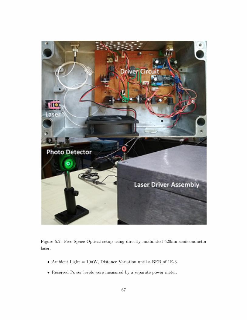
Figure 5.2: Free Space Optical setup using directly modulated 520nm semiconductor
laser.
• Ambient Light = 10uW, Distance Variation until a BER of 1E-3.
• Received Power levels were measured by a separate power meter.
67
• Average optical power was calculated by taking weighted average of high and low
power levels. For 4-PPM, avg rx power = (high + 3xlow)/4
Figure 5.3: LI characteristics of 520nm Laser diode depicting direct modulation with
80mA bias and 30mA swing.
Distance(cm) Low(uW) High(uW) Average(uW) Bit Error Rate
90 29 92 45 0.00
100 23 74 36 6.16× 10⁻⁷
110 19 65 31 6.78× 10⁻⁶
120 18 57 28 6.34× 10⁻⁵
130 16 49 24 1.76× 10⁻⁴
140 13 42 20 6.47× 10⁻⁴
Table 5.2: BER at different received power levels with varying distance between trans-
mitter and receiver for 4-PPM modulation.
68
Figure 5.4: BER vs Received Power for 4-PPM directly modulated 520nm LASER in
Free-space
Results and Discussion:
• The BER curve, Figure 5.4, shows that 10uW power was sufficient to get a
BER of 1.00E-3 while using PPM-4 modulation. However, there were few major
issues with the experimental setup which could have compromised the system
performance.
• Firstly, the power measurements might not be accurate because the two devices,
the detector (which receives the signal) and the power meter(which measures the
power) may have alignment difference when they are placed in the set-up.
• Secondly, as the power measurement and BER evaluation were done using two
different devices, there would be an inherent offset in the power measurement,
which can not be neglected at such low power levels.
• Lastly, the ambient light levels were considerably high and fluctuating compared
to the operating power levels.
69
5.3 Experiment II: PPM-Optical Back to Back using VOA
(532nm LASER I with EOM):
This experiment was also conducted in the Lab at very low ambient light conditions.
For testing the BER performance at different received power levels, the optical signal
was sent through a variable optical attenuator (VOA) in free space and captured by
the detector at a fixed distance. Hardware test set-up for this experiment is shown in
Figure 5.5 and 5.6. Observation table and test conditions are mentioned as following.
Test conditions and Observations:
• Modulation = External, EOM Swing = 128V, Extinction = 6dB (Figure 5.7)
• Receiver Gain = 10 dB, Receiver Coupling = AC, Receiver Bandwidth = 1.4MHz
• Ambient Light ≈ 6.4uW, Attenuation Variation until a BER of 1E-3
• Average Received power was measured by checking the DC level of detector out-
put with no modulation, as the modulator bias was adjusted to get average mod-
ulated signal did not have any DC.
• Avg. Rx Power = ( Average DC - Ambient DC)/Detector Conversion
(Figure 5.8).
Figure 5.5: Complete experimental setup with all electrical and optical components
used in experiments II, III and IV.
70
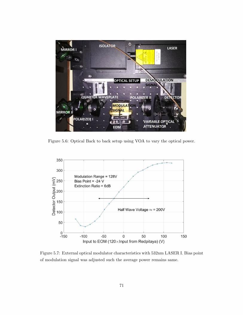
Figure 5.6: Optical Back to back setup using VOA to vary the optical power.
Figure 5.7: External optical modulator characteristics with 532nm LASER I. Bias point
of modulation signal was adjusted such the average power remains same.
71
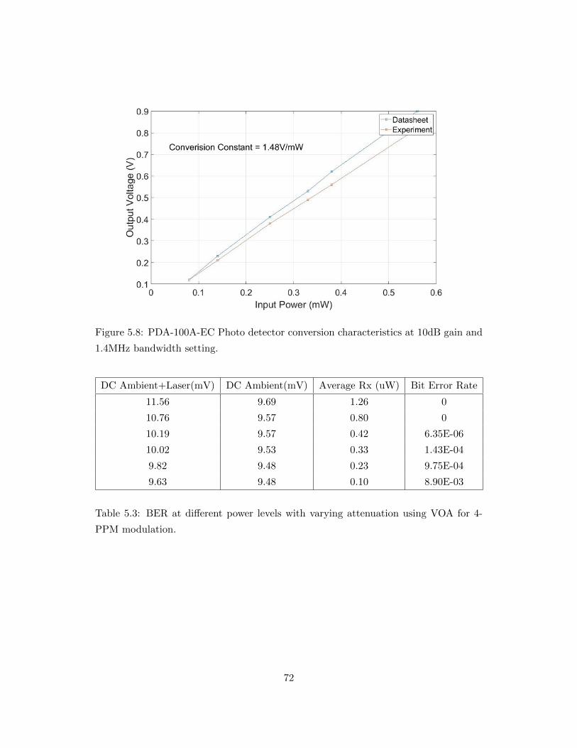
Figure 5.8: PDA-100A-EC Photo detector conversion characteristics at 10dB gain and
1.4MHz bandwidth setting.
DC Ambient+Laser(mV) DC Ambient(mV) Average Rx (uW) Bit Error Rate
11.56 9.69 1.26 0
10.76 9.57 0.80 0
10.19 9.57 0.42 6.35E-06
10.02 9.53 0.33 1.43E-04
9.82 9.48 0.23 9.75E-04
9.63 9.48 0.10 8.90E-03
Table 5.3: BER at different power levels with varying attenuation using VOA for 4-
PPM modulation.
72
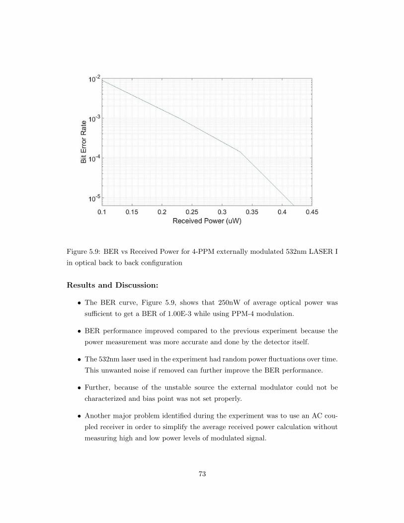
Figure 5.9: BER vs Received Power for 4-PPM externally modulated 532nm LASER I
in optical back to back configuration
Results and Discussion:
• The BER curve, Figure 5.9, shows that 250nW of average optical power was
sufficient to get a BER of 1.00E-3 while using PPM-4 modulation.
• BER performance improved compared to the previous experiment because the
power measurement was more accurate and done by the detector itself.
• The 532nm laser used in the experiment had random power fluctuations over time.
This unwanted noise if removed can further improve the BER performance.
• Further, because of the unstable source the external modulator could not be
characterized and bias point was not set properly.
• Another major problem identified during the experiment was to use an AC cou-
pled receiver in order to simplify the average received power calculation without
measuring high and low power levels of modulated signal.
73
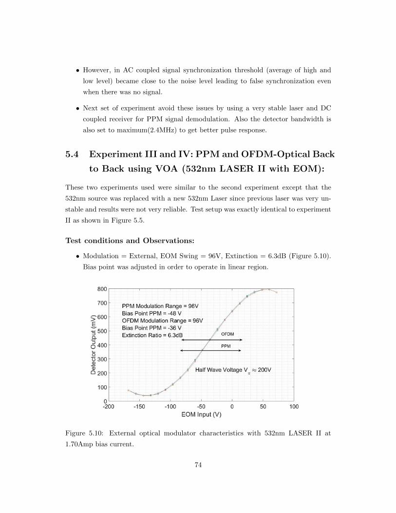
• However, in AC coupled signal synchronization threshold (average of high and
low level) became close to the noise level leading to false synchronization even
when there was no signal.
• Next set of experiment avoid these issues by using a very stable laser and DC
coupled receiver for PPM signal demodulation. Also the detector bandwidth is
also set to maximum(2.4MHz) to get better pulse response.
5.4 Experiment III and IV: PPM and OFDM-Optical Back
to Back using VOA (532nm LASER II with EOM):
These two experiments used were similar to the second experiment except that the
532nm source was replaced with a new 532nm Laser since previous laser was very un-
stable and results were not very reliable. Test setup was exactly identical to experiment
II as shown in Figure 5.5.
Test conditions and Observations:
• Modulation = External, EOM Swing = 96V, Extinction = 6.3dB (Figure 5.10).
Bias point was adjusted in order to operate in linear region.
Figure 5.10: External optical modulator characteristics with 532nm LASER II at
1.70Amp bias current.
74
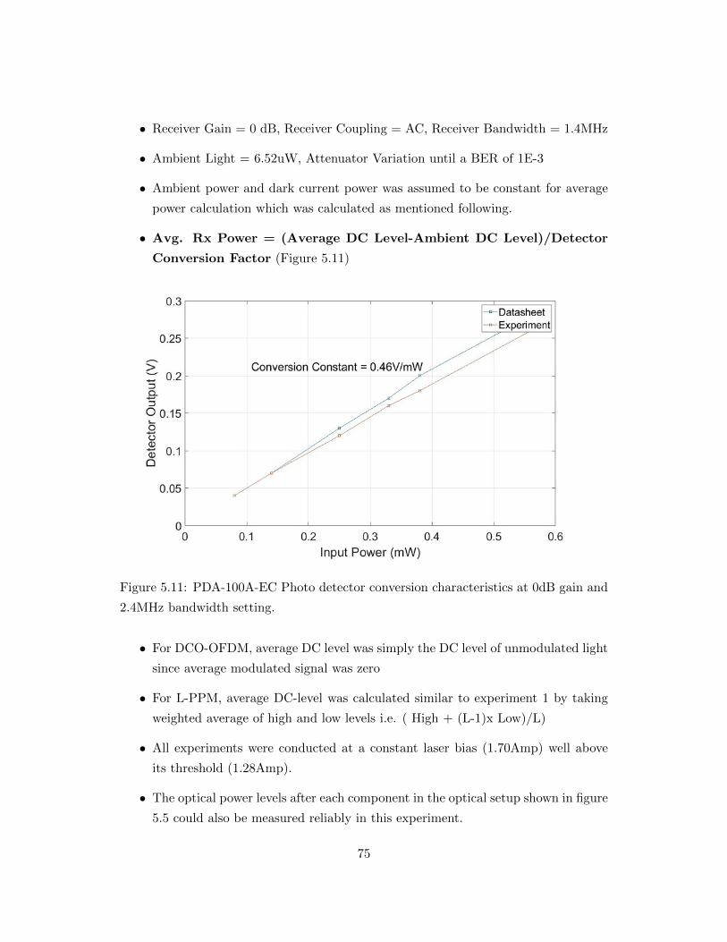
• Receiver Gain = 0 dB, Receiver Coupling = AC, Receiver Bandwidth = 1.4MHz
• Ambient Light = 6.52uW, Attenuator Variation until a BER of 1E-3
• Ambient power and dark current power was assumed to be constant for average
power calculation which was calculated as mentioned following.
• Avg. Rx Power = (Average DC Level-Ambient DC Level)/Detector
Conversion Factor (Figure 5.11)
Figure 5.11: PDA-100A-EC Photo detector conversion characteristics at 0dB gain and
2.4MHz bandwidth setting.
• For DCO-OFDM, average DC level was simply the DC level of unmodulated light
since average modulated signal was zero
• For L-PPM, average DC-level was calculated similar to experiment 1 by taking
weighted average of high and low levels i.e. ( High + (L-1)x Low)/L)
• All experiments were conducted at a constant laser bias (1.70Amp) well above
its threshold (1.28Amp).
• The optical power levels after each component in the optical setup shown in figure
5.5 could also be measured reliably in this experiment.
75
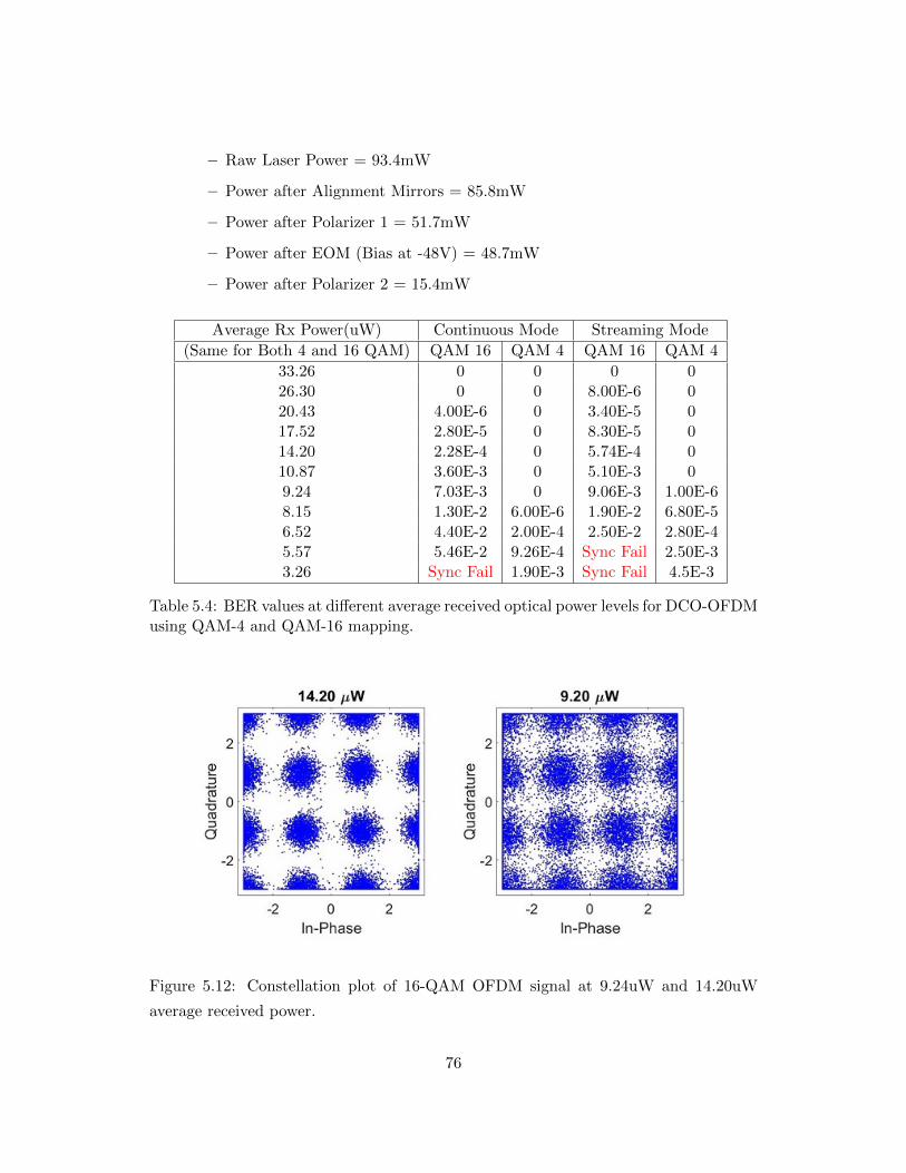
– Raw Laser Power = 93.4mW
– Power after Alignment Mirrors = 85.8mW
– Power after Polarizer 1 = 51.7mW
– Power after EOM (Bias at -48V) = 48.7mW
– Power after Polarizer 2 = 15.4mW
Average Rx Power(uW) Continuous Mode Streaming Mode
(Same for Both 4 and 16 QAM) QAM 16 QAM 4 QAM 16 QAM 4
33.26 0 0 0 026.30 0 0 8.00E-6 020.43 4.00E-6 0 3.40E-5 017.52 2.80E-5 0 8.30E-5 014.20 2.28E-4 0 5.74E-4 010.87 3.60E-3 0 5.10E-3 09.24 7.03E-3 0 9.06E-3 1.00E-68.15 1.30E-2 6.00E-6 1.90E-2 6.80E-56.52 4.40E-2 2.00E-4 2.50E-2 2.80E-45.57 5.46E-2 9.26E-4 Sync Fail 2.50E-33.26 Sync Fail 1.90E-3 Sync Fail 4.5E-3
Table 5.4: BER values at different average received optical power levels for DCO-OFDMusing QAM-4 and QAM-16 mapping.
Figure 5.12: Constellation plot of 16-QAM OFDM signal at 9.24uW and 14.20uW
average received power.
76
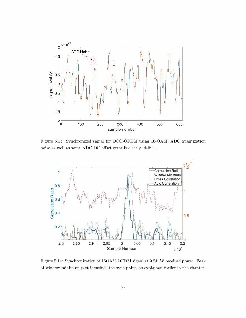
Figure 5.13: Synchronized signal for DCO-OFDM using 16-QAM. ADC quantization
noise as well as some ADC DC offset error is clearly visible.
Figure 5.14: Synchronization of 16QAM OFDM signal at 9.24uW received power. Peak
of window minimum plot identifies the sync point, as explained earlier in the chapter.
77
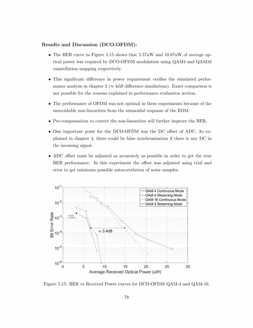
Results and Discussion (DCO-OFDM):
• The BER curve in Figure 5.15 shows that 5.57uW and 10.87uW of average op-
tical power was required by DCO-OFDM modulation using QAM4 and QAM16
constellation mapping respectively.
• This significant difference in power requirement verifies the simulated perfor-
mance analysis in chapter 2 (≈ 4dB difference simulations). Exact comparison is
not possible for the reasons explained in performance evaluation section.
• The performance of OFDM was not optimal in these experiments because of the
unavoidable non-linearities from the sinusoidal response of the EOM.
• Pre-compensation to correct the non-linearities will further improve the BER.
• One important point for the DCO-OFDM was the DC offset of ADC. As ex-
plained in chapter 4, there could be false synchronization if there is any DC in
the incoming signal.
• ADC offset must be adjusted as accurately as possible in order to get the true
BER performance. In this experiment the offset was adjusted using trial and
error to get minimum possible autocorrelation of noise samples.
Figure 5.15: BER vs Received Power curves for DCO-OFDM QAM-4 and QAM-16.
78
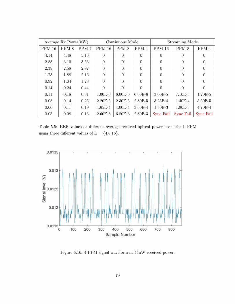
Average Rx Power(uW) Continuous Mode Streaming Mode
PPM-16 PPM-8 PPM-4 PPM-16 PPM-8 PPM-4 PPM-16 PPM-8 PPM-4
4.14 4.48 5.16 0 0 0 0 0 0
2.83 3.10 3.63 0 0 0 0 0 0
2.39 2.58 2.97 0 0 0 0 0 0
1.73 1.88 2.16 0 0 0 0 0 0
0.92 1.04 1.28 0 0 0 0 0 0
0.14 0.24 0.44 0 0 0 0 0 0
0.11 0.18 0.31 1.00E-6 6.00E-6 6.00E-6 3.00E-5 7.10E-5 1.20E-5
0.08 0.14 0.25 2.20E-5 2.30E-5 2.80E-5 3.25E-4 1.40E-4 5.50E-5
0.06 0.11 0.19 4.65E-4 4.00E-4 3.60E-4 1.50E-3 1.90E-3 4.70E-4
0.05 0.08 0.13 2.60E-3 6.80E-3 2.80E-3 Sync Fail Sync Fail Sync Fail
Table 5.5: BER values at different average received opitcal power levels for L-PPM
using three different values of L = {4,8,16}.
Figure 5.16: 4-PPM signal waveform at 44uW received power.
79
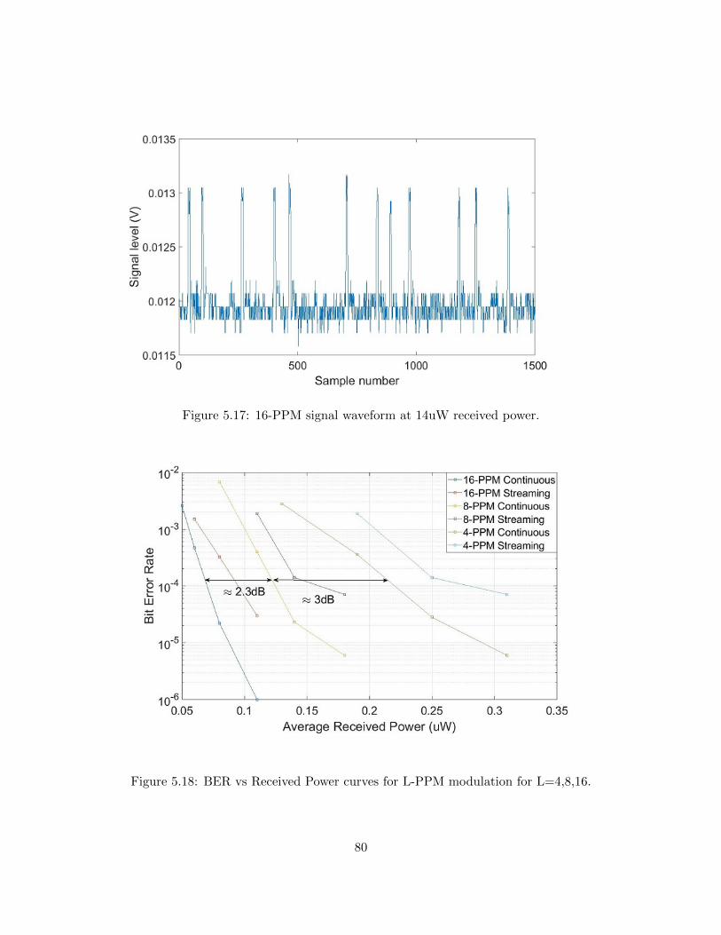
Figure 5.17: 16-PPM signal waveform at 14uW received power.
Figure 5.18: BER vs Received Power curves for L-PPM modulation for L=4,8,16.
80
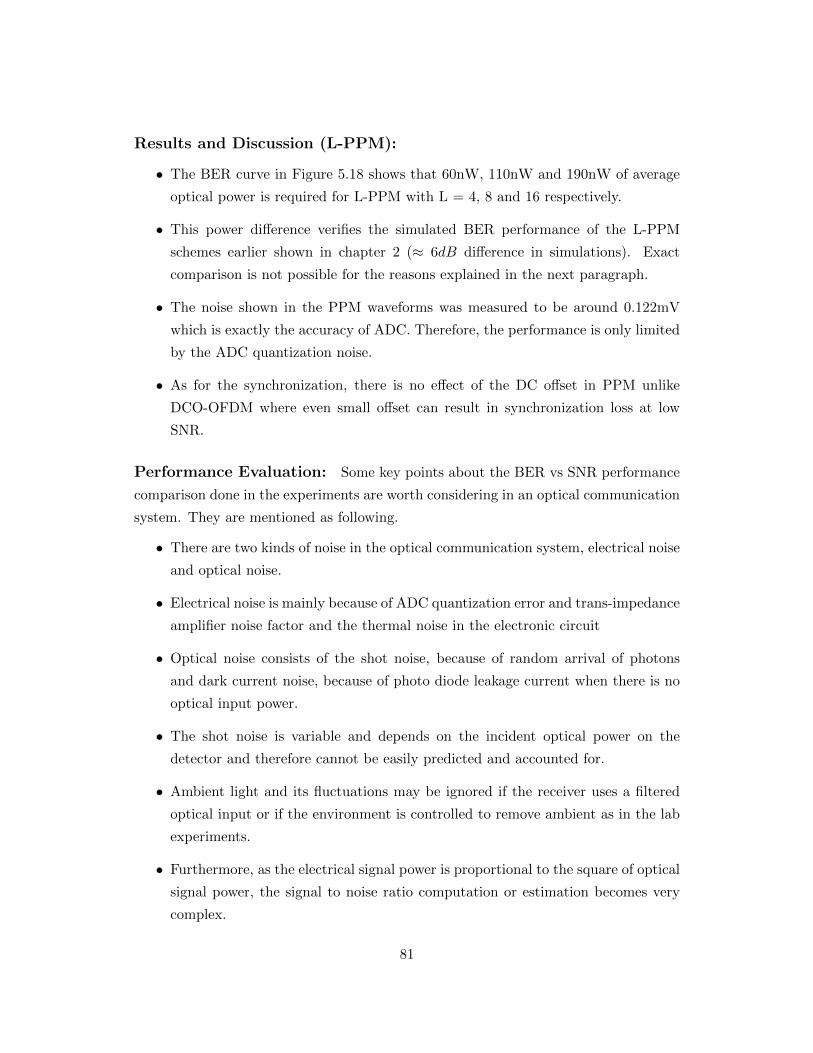
Results and Discussion (L-PPM):
• The BER curve in Figure 5.18 shows that 60nW, 110nW and 190nW of average
optical power is required for L-PPM with L = 4, 8 and 16 respectively.
• This power difference verifies the simulated BER performance of the L-PPM
schemes earlier shown in chapter 2 (≈ 6dB difference in simulations). Exact
comparison is not possible for the reasons explained in the next paragraph.
• The noise shown in the PPM waveforms was measured to be around 0.122mV
which is exactly the accuracy of ADC. Therefore, the performance is only limited
by the ADC quantization noise.
• As for the synchronization, there is no effect of the DC offset in PPM unlike
DCO-OFDM where even small offset can result in synchronization loss at low
SNR.
Performance Evaluation: Some key points about the BER vs SNR performance
comparison done in the experiments are worth considering in an optical communication
system. They are mentioned as following.
• There are two kinds of noise in the optical communication system, electrical noise
and optical noise.
• Electrical noise is mainly because of ADC quantization error and trans-impedance
amplifier noise factor and the thermal noise in the electronic circuit
• Optical noise consists of the shot noise, because of random arrival of photons
and dark current noise, because of photo diode leakage current when there is no
optical input power.
• The shot noise is variable and depends on the incident optical power on the
detector and therefore cannot be easily predicted and accounted for.
• Ambient light and its fluctuations may be ignored if the receiver uses a filtered
optical input or if the environment is controlled to remove ambient as in the lab
experiments.
• Furthermore, as the electrical signal power is proportional to the square of optical
signal power, the signal to noise ratio computation or estimation becomes very
complex.
81
• Hence the experimental BER performance has been evaluated against the average
received optical power which is easier to measure.
• Further since the simulation model presented in chapter 2 assume a Single White
Guassian noise model and plots the BER curves with respect to the ratio of the
electrical energy per bit to the noise power density.
• Therefore a direct comparison between the simulated and the experimental BER
curves would not be meaningful. However, the similarities will be there in the
results which are mentioned in the results and discussion for each experiment.
5.5 Conclusion:
From the experiments conducted so far, it was observed that all schemes perform well at
micro-Watts levels of optical power and provide a BER of 1.0E-3 or better. Regarding
OFDM vs PPM performance, the lowest order PPM modulation (PPM4) outperforms
the best QAM DCO OFDM as it requires only 0.13uW of power as compared 10.87uW
for DCO-OFDM (≈ 100 times less) difference) while achieving more than 70% of the
data-rate of QAM4 based DCO-OFDM.
However, these free-space channel experiments are not sufficient to evaluate the
performance of the two modulation schemes. True performance comparison can only be
done in an actual multipath under water channel. In presence of multipath, OFDM will
edge out in the performance because its robustness against inter-symbol interference
and linear channel equalization which will be more difficult for PPM.
Nevertheless in a free space LOS channel, it can be established that PPM has far
better BER performance while operating at moderate data rates. Hence it can be
concluded that unless there is large multipath (which has not yet been established)
PPM would be a preferred modulation scheme if data rate requirement is not very
high.
5.6 Future Work:
The major part of the transceiver software implementation has been completed how-
ever, for actual deployment of the design there are several modifications and actual
experiments needed to be conducted going forward. Some of the key tasks for the
future continuation of this work are mentioned below.
82
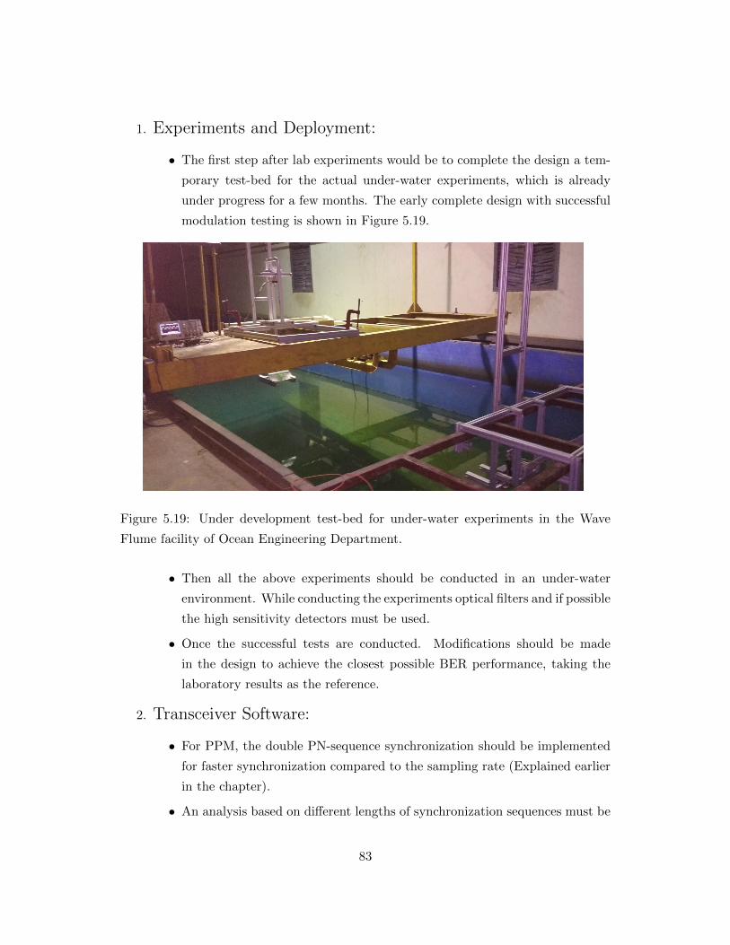
1. Experiments and Deployment:
• The first step after lab experiments would be to complete the design a tem-
porary test-bed for the actual under-water experiments, which is already
under progress for a few months. The early complete design with successful
modulation testing is shown in Figure 5.19.
Figure 5.19: Under development test-bed for under-water experiments in the Wave
Flume facility of Ocean Engineering Department.
• Then all the above experiments should be conducted in an under-water
environment. While conducting the experiments optical filters and if possible
the high sensitivity detectors must be used.
• Once the successful tests are conducted. Modifications should be made
in the design to achieve the closest possible BER performance, taking the
laboratory results as the reference.
2. Transceiver Software:
• For PPM, the double PN-sequence synchronization should be implemented
for faster synchronization compared to the sampling rate (Explained earlier
in the chapter).
• An analysis based on different lengths of synchronization sequences must be
83
done to decide the optimum length sequence thus making the synchroniza-
tion robust at low SNR values.
• For PPM, other variants of the PPM discussed in the chapter 2 can also be
implemented to get better data-rates in PPM.
• For OFDM, studies must be conducted to ascertain whether using the sync
sequence as the actual pilot in actual channel will pose any issue or not.
If yes, then a separate pilot overhead must be added in the OFDM frame
structure (MATLAB-Codes have already been written for separate pilot).
• Inverse sinusoidal (or other similar) pre-compensation should be implemented
to enable full utilization of modulation depth of the EOM including the non-
linear region.
• Channel coding which has been hardly touched upon during the course of
the whole implementation should be the main focus for the software part in
the future to enable error free communication.
3. Transceiver Hardware:
• The AOM has not been yet used because of alignment issue. Once the issue is
resolved, AOM should be characterized similar to EOM and output response
must be compared for both to decide the better modulator for experiments.
• New electrical boards with higher sampling rates and ADC accuracy if pos-
sible should be tested with existing transceiver software.
• All the codes are written in C hence can be deployed easily onto any other
board capable of running C binaries.
• For transmitter optics, the collimator should be replaced or an additional
focusing optics should be used with the existing collimator to get a much
better collimated beam.
• The power characterization and modulation testing done so far using the
early design of under-water test-bed has established that geometric loss is
more significant than the actual channel loss.
• Receiver optics is another area that needs real attention as the manual align-
ment of the receiver has been a bottle neck for the under-water experiments.
• The combined pre-amplifier circuits for EOM, AOM and Laser must be
rebuilt on a actual PCB to improve the quality of the modulated electrical
signal.
84
Bibliography
[1] Hemani Kaushal and Georges Kaddum, Underwater Optical Wireless Communica-
tion, IEEE Access, 2016.
[2] Majed M. Albogame and Khaled Elleithy, Enhancement Orthogonal Frequency
Division Multiplexing (OFDM) in Wireless Communication Network by Using
PTS(Partial Transmit Sequences) Technique,29th International Conference on
Computers and Their Applications, Las Vegas, Nevada, March, 2014
[3] Sarangi Devasmitha Dissanayake and Jean Armstrong on Comparison of ACO-
OFDM, DCO-OFDM and ADO-OFDM in IM/DD Systems, Journal of Lightwave
Technology, Vol. 31, No. 7, April 1, 2013
[4] Jean Armtrong on OFDM for Optical Communications, Journal of Lightwave Tech-
nology, Vol. 27, No. 3, February 1, 2009
[5] Krishna Shankar, Symbol Error rate for QAM (16, 64, 256,.., M-QAM),
http://www.dsplog.com/2012/01/01/symbol-error-rate-16qam-64qam-256qam/
[6] Bahaa E. A. Saleh. and Malvin Carl Teich, Amplifier Non-Linearity, Section 14.4,
Fundamentals of Photonics, 2nd Edition, John Wiley & Sons Publications, 2007
[7] https://www.redpitaya.com/f145/oscilloscope-signal-generator/
specifications
[8] http://redpitaya.readthedocs.io/en/latest/quickStart/first.html
[9] https://people.cs.uct.ac.za/~ksmith/articles/sliding_window_minimum.
html
85