Embed Size (px)
Citation preview

1
1
Hardware Design I Chap. 2Basis of logical circuit, logical
expression, and logical function
Computing Architecture Lab.Hajime Shimada
E-mail: [email protected]
Hardware Design I (Chap. 2) 2Computing Architecture Lab.
Hajime Shimada
Outline
Combinational logical circuitLogic gate (logic element)Definition of combinational logical circuitHow to create output signal?
Logical functionDefinition of logical functionRelationship between logical circuit
Logical expressionDefinition of logical expressionMinterm and maxtermAxiomatic systemsAmount of logical expression

2
Hardware Design I (Chap. 2) 3Computing Architecture Lab.
Hajime Shimada
Review: outlined flow of LSI design
Define specificationDefinition in hardware description language
Architectural design
Circuit with basic logic gatesLogical design
Mask patternPhysical design
Manufacturing
Logic synthesis
Place and routeThis chapter treats
this area•Logical function•Logical expression
Hardware Design I (Chap. 2) 4Computing Architecture Lab.
Hajime Shimada
Relationship between technical terms
If we minimize logical expression, we can implement minimized logical circuit
Logical expression 1
Logical expression 2
Logicalcircuit 1Logical circuit 2......
Specification
Logicalfunction Truth table
In this section,please assumecombinationallogical circuit

3
Hardware Design I (Chap. 2) 5Computing Architecture Lab.
Hajime Shimada
Detailed talk of logical design
Specification of sequential machine
Specification of logical function
Logical expression
Simplified logical expression= Basic logic gates
•Simplify of two level logic•Simplify of multi level logic
-> Chap. 6
-> later Chap. 2
-> later Chap. 2
-> Chap. 3 and 7
-> Chap. 7 and 8
Hardware Design I (Chap. 2) 6Computing Architecture Lab.
Hajime Shimada
Logic gate (logic element)
The electric circuit witch outputs result of logical operation
e.g. NOT, NANDBoth inputs and outputs can only take 0 or 1
x Q0
x Q11 0
xQ
y
NOT gate NAND gate Circuit symbol
Circuit symbol
-> Chap. 1

4
Hardware Design I (Chap. 2) 7Computing Architecture Lab.
Hajime Shimada
NOT, AND, and OR on Boolean algebra
Logical circuit operates on Boolean algebraHere’s basic logic from Boolean algebra
x Q0 11 0
x Qx
y
Qx
y
Q
x y Q0 0 00 1 01 0 01 1 1
x y Q0 0 00 1 11 0 11 1 1
NOTAND OR
Hardware Design I (Chap. 2) 8Computing Architecture Lab.
Hajime Shimada
NOT, AND, and OR on Venn diagram
In some case, imaging Venn diagram helps understanding
NOT: left areaAND: shared areaOR: sum of area
A・B A+BAA

5
Hardware Design I (Chap. 2) 9Computing Architecture Lab.
Hajime Shimada
NAND and NOR on Boolean algebra
Physical implementation is easyUsually, AND and OR are implemented by combining NOT and NAND/NOR
x
y
Qx
y
Q
x y Q0 0 10 1 11 0 11 1 0
x y Q0 0 10 1 01 0 01 1 0
NAND
= OR
The circle represents negation
= AND
NOR
-> Chap. 1
Hardware Design I (Chap. 2) 10Computing Architecture Lab.
Hajime Shimada
Combinational logical circuit
The signal flow must be contra flowThe output of the gate will be defined from input sideThe output is defined with current input
No loop in itIt is also called “acyclic circuit”
Inpu
ts
Out
put
Signal flow

6
Hardware Design I (Chap. 2) 11Computing Architecture Lab.
Hajime Shimada
Let’s assume looped logic circuit (1/2)
It sometimes gives unstable outputLet’s assume 1 is inputted under 0 output status
Let’s assume 1 is inputted under 1 output status
Input Output0
1 10
1
Input Output1
1 01
0
The output switches 0/1 forever!!! ->oscillator
Hardware Design I (Chap. 2) 12Computing Architecture Lab.
Hajime Shimada
Let’s assume looped logic circuit (2/2)
We rarely achieve stable circuit with looped combinational circuit
Let’s assume 1 is inputted under 1 output statusIt continues to output 1
Once input falls to 0, the output changes to 0 forever
InputOutput1->0
0 0->11->0
InputOutput1
1 01
Usually, they are rare and utilization is limited...How to crate loop?-> Sequential circuit
(Chap. 6)

7
Hardware Design I (Chap. 2) 13Computing Architecture Lab.
Hajime Shimada
Definition of combinational logic with directed graph
Set of vertices: V={a, b, c, d, e, f, g, h}Set of edges: E⊆(V×V)E={(a,e), (b,e), (b,d), (c,f), (d,f), (e,g), (f,g), (g,h)}Label of vertex:NOT, NAND, and so on
NOT
NAND
NAND
NANDa
b
cd
e
f g h
Hardware Design I (Chap. 2) 14Computing Architecture Lab.
Hajime Shimada
If you felt “what is directed graph?” ...
Please relearn “graph theory”The sets of vertices and edgese.g. network connection graph, schematic diagram, ...Specific graph: tree, directed graph, weighted graph, ...
It is widely used in informatics worldSyntax tree (compiler)Markov chain (voice recognition)Perceptron (neural network)

8
Hardware Design I (Chap. 2) 15Computing Architecture Lab.
Hajime Shimada
About technical terms of set theory
SetGathered set of elementse.g. {0, 1}, {a, b, ..., z}, ...
Cartesian productA set of ordered pairs of elementsNotation: A × B (A,B: set)e.g. {0, 1} × {a, b} = {(0,a), (0,b), (1,a), (1,b)}Other notation: V2, {0, 1}2
Hardware Design I (Chap. 2) 16Computing Architecture Lab.
Hajime Shimada
The syntax of combinational logic from graph theory
Directed Acyclic Graph (DAG): (V, E)V: set of verticesE: set of edges, subset of (V × V)
(V × V) denotes set of Cartesian product
Allocate logic gate (e.g. NAND) label to verticesAllocate 1 label to 1 vertex

9
Hardware Design I (Chap. 2) 17Computing Architecture Lab.
Hajime Shimada
Terms of combinational logic (1/3)
Fan-in: a input side of edgee.g. v1 is the fan-in of edge (v1, v2) Viewpoint from the v2 side
Fan-out: a output side of edge (v1, v2) e.g. v2 is the fan-out of edge (v1, v2)
NOT
NAND
NAND
NANDa
b
cd
e
f g h
fan-in
fan-out
primaryoutput
primary input
path
Hardware Design I (Chap. 2) 18Computing Architecture Lab.
Hajime Shimada
Terms of combinational logic (2/3)
Primary input: a vertex which does not have fan-inPrimary output: a vertex which does not have
fan-out
NOT
NAND
NAND
NANDa
b
cd
e
f g h
primaryoutput
primary input
path
fan-in
fan-out

10
Hardware Design I (Chap. 2) 19Computing Architecture Lab.
Hajime Shimada
Terms of combinational logic (3/3)
Path: a set of edges from primary input to primary output
e.g. (v1, v2) (v2, v3) ... (vn-1, vn)v1 is transitive fan-invn is transitive fan-out
NOT
NAND
NAND
NANDa
b
cd
e
f g h
primaryoutput
primary input
path
fan-in
fan-out
Hardware Design I (Chap. 2) 20Computing Architecture Lab.
Hajime Shimada
Value allocation to logic circuit
Value allocationAllocate 0/1 value to (output of) each vertexAdequate allocation: satisfies the truth of gate
The allocation will be defined if all of primary input has definedIt is also called logic simulation
0
10
1
NOT
NANDa
b
0
11
0
NOT
NANDa
b
Adequate allocation Not adequate allocation

11
Hardware Design I (Chap. 2) 21Computing Architecture Lab.
Hajime Shimada
The algorithm of value allocation
1. Define the value of primary inputsPrimary inputs are called level 0 vertices
2. Define the value of level 1 verticesLevel 1 vertices: all inputs of them are primary inputAll inputs value are already defined in 1.
3. Define the value of level 2 verticesLevel 2 vertices: all inputs of them are less than level 1 (level 0 or 1)
4. Define level n vertices until the all of the vertices have defined
Level n vertices: all inputs of them are less than level n-1
Hardware Design I (Chap. 2) 22Computing Architecture Lab.
Hajime Shimada
Example of value allocation (1/4)
Allocate value to primary inputs (level 0 vertices)We can allocate them without constraintUsually, they are given
0
1
1
NOT
NAND
NAND
NANDa
b
cd
e
f g h
Level 0 Level 1
Level 2
Level 3

12
Hardware Design I (Chap. 2) 23Computing Architecture Lab.
Hajime Shimada
Example of value allocation (2/4)
Allocate values to level 1 verticesWhich are only connected to primary inputs
0
1
10
1
NOT
NAND
NAND
NANDa
b
cd
e
f g h
Level 0 Level 1
Level 2
Level 3
Hardware Design I (Chap. 2) 24Computing Architecture Lab.
Hajime Shimada
Example of value allocation (3/4)
Allocate values to level 2 verticesWhich are only connected to less than level 1 verticesSee the vertices which values have already allocated
0
1
10
1
1NOT
NAND
NAND
NANDa
b
cd
e
f g h
Level 0 Level 1
Level 2
Level 3

13
Hardware Design I (Chap. 2) 25Computing Architecture Lab.
Hajime Shimada
Example of value allocation (4/4)
Allocate value to level 3 verticesWhich are only connected to less than level 2 verticesThe allocation of primary outputs are the same to the prior vertices
0
1
10
1
10NOT
NAND
NAND
NANDa
b
cd
e
f g0
h
Level 0 Level 1
Level 2
Level 3
Hardware Design I (Chap. 2) 26Computing Architecture Lab.
Hajime Shimada
Short exercise
Allocate values to left verticesIf you left time, add level notations to the vertices
0
1
1
NAND
NAND
NAND
NAND
NAND
NAND
NAND
NAND

14
Hardware Design I (Chap. 2) 27Computing Architecture Lab.
Hajime Shimada
The answer of short exercise
0
1
1
1
NAND
NAND
NAND
NAND
NAND
NAND
NAND
NAND
1
0
1
01
1
0
Level 1
Level 2
Level 2
Level 3
Level 4
Level 5
Level 5
Level 6
0
Hardware Design I (Chap. 2) 28Computing Architecture Lab.
Hajime Shimada
Outline
Combinational logical circuitLogic gate (logic element)Definition of combinational logical circuitHow to create output signal?
Logical functionDefinition of logical functionRelationship between logical circuit
Logical expressionDefinition of logical expressionMinterm and maxtermAxiomatic systemsAmount of logical expression

15
Hardware Design I (Chap. 2) 29Computing Architecture Lab.
Hajime Shimada
Definition of logical function from mathematical viewpoint
Representation of the relationship between input value and output valueThe definition of n-value logical function:Projection from {0, 1}n to {0, 1}
Subset f ⊆ {0, 1}n × {0, 1} which does not include both (X, 0) ∈ f and (X, 1) ∈ f in arbitrary XWe denote it y = f(X) if (X, y) ∈ f{0, 1}n is called domain{0, 1} is called codomain
Hardware Design I (Chap. 2) 30Computing Architecture Lab.
Hajime Shimada
Example of definition of 3-value logical function (notated by logical circuit)
It outputs 0 if we input (0, 0, 0) into itIt outputs 1 if we input (0, 0, 1) into it
It outputs 1 if we input (1, 1, 1) into it
Inpu
ts
...
This is logical function!
Out
put

16
Hardware Design I (Chap. 2) 31Computing Architecture Lab.
Hajime Shimada
Examples of definition of representative logical function
The function of NOT ⊆ {0,1}×{0,1}{(0, 1), (1, 0)}
The function of AND ⊆ {0,1}2×{0,1}{((0, 0), 0), ((0, 1), 0), ((1, 0), 0), ((1, 1), 1)}
The function of AND ⊆ {0,1}2×{0,1}{((0, 0), 0), ((0, 1), 1), ((1, 0), 1), ((1, 1), 1)}
Input Output
Hardware Design I (Chap. 2) 32Computing Architecture Lab.
Hajime Shimada
Hot to denote them in usual?
Usually, we do not use mathematical definitionWe usually use following notations
Logical circuitTruth tableLogical expression

17
Hardware Design I (Chap. 2) 33Computing Architecture Lab.
Hajime Shimada
Truth table
One of the representation style of logical functionAligning output values for all possible inputsThe size of n values logical function is 2n
x1 x2 f(x1,x2) g(x1,x2) h(x1,x2)0 0 0 0 h(0, 0)0 1 0 1 h(0, 1)1 0 0 1 h(1, 0)1 1 1 0 h(1, 1)
Logical function Truth tableOne for onerelationship
If truth tables of two functions are identical, the functions are identical
Hardware Design I (Chap. 2) 34Computing Architecture Lab.
Hajime Shimada
Relationship between logical function and logical circuit
Logical function represents the relationship of input value and output value in combinational logical circuit
x1 yx2
y
x1
x2
x1 x2 y0 0 00 1 01 0 01 1 1
Relationshipof input/output
Many correspondinglogical circuits
Logical function y
Truth table

18
Hardware Design I (Chap. 2) 35Computing Architecture Lab.
Hajime Shimada
Relationship between technical terms
If we minimize logical expression, we can implement minimized logical circuit
Logical expression 1
Logical expression 2
Logicalcircuit 1Logical circuit 2......
Specification
Logicalfunction Truth table
Many possible candidatesfor these!
EqualUnique
Hardware Design I (Chap. 2) 36Computing Architecture Lab.
Hajime Shimada
Multiple output logical function
In many case, digital system has multiple outputsUsually, we decompose it to multiple single output function for simplicity
Out
puts
Inpu
ts

19
Hardware Design I (Chap. 2) 37Computing Architecture Lab.
Hajime Shimada
Truth table of multiple output logical function
Multiple output function (m outputs):Projection from {0, 1}n to {0, 1}m
List of m projections from {0, 1}n to {0, 1}
x1 x2 f0(x1,x2) f1(x1,x2)
0 0 0 00 1 0 11 0 0 11 1 1 0
Hardware Design I (Chap. 2) 38Computing Architecture Lab.
Hajime Shimada
Operation between logical functions
We can extend operation on logical value to logical function
(f ・ g) (x1, x2, ..., xn) = f(x1, ..., xn) ・ g(x1,..., xn)(f + g) (x1, x2, ..., xn) = f(x1, ..., xn) + g(x1,..., xn)(f') (x1, x2, ..., xn) = f(x1, x2, ..., xn)‘
Detail is taught in following logical expression section

20
Hardware Design I (Chap. 2) 39Computing Architecture Lab.
Hajime Shimada
Summary of logical function
It is a function from {0, 1}n to {0, 1}{0, 1}n×{0,1} with some constraint
It is represented uniquely with truth tableList of relationship between all inputs and outputsBut it requires 2n size of memory
We can apply operation on it Logical function:The relationship betweeninputs and outputs
Hardware Design I (Chap. 2) 40Computing Architecture Lab.
Hajime Shimada
Outline
Combinational logical circuitLogic gate (logic element)Definition of combinational logical circuitHow to create output signal?
Logical functionDefinition of logical functionRelationship between logical circuit
Logical expressionDefinition of logical expressionMinterm and maxtermAxiomatic systemsAmount of logical expression

21
Hardware Design I (Chap. 2) 41Computing Architecture Lab.
Hajime Shimada
Logical expression
One of the expression of logical functionRepresent it with arrangement of variable which denotes logical functione.g. x + y・z + x・y’・z’
Efficient than truth tableBut there’s no uniquenessx = a+b; y = c・d; z = x+y -> z = (a+b) + (c・d)
abcd
xz
a+bx+y
ab
xz
y c・dcd y
Hardware Design I (Chap. 2) 42Computing Architecture Lab.
Hajime Shimada
The definition of logical expression
1. Logical variables are logical expressione.g. x, y, z, x1, x2, a, b, ...
2. If E1 and E2 are logical expression, (E1・E2), (E1+E2), (E1') are logical expression
e.g. (x・y), (x+y), (x+(y・z)), (x+(y'))
Generated in recursively We can omit brackets by adding order to operations
Order: ', ・, and +

22
Hardware Design I (Chap. 2) 43Computing Architecture Lab.
Hajime Shimada
The expression of logical function with logical expression (1/2)
Pay attention to the logical function which has only one “1” output in truth table
Called mintermMinterm can be represented by AND and NOT
x y x’・y’ x’・y x・y’ x・y0 0 1 0 0 0 0 1 0 1 0 0 1 0 0 0 1 0 1 1 0 0 0 1
Minterm
Hardware Design I (Chap. 2) 44Computing Architecture Lab.
Hajime Shimada
The expression of logical function with logical expression (2/2)
The logical function which has multiple “1”output is represented by OR of mintermsThe arbitrary function can be represented with AND, OR, and NOT of logical variable
x y x’・y’ x’・y x・y’ x・y f(x,y)0 0 1 0 0 0 00 1 0 1 0 0 11 0 0 0 1 0 11 1 0 0 0 1 0
= x’・y + x・y’
Minterm

23
Hardware Design I (Chap. 2) 45Computing Architecture Lab.
Hajime Shimada
Notation only 2-input NAND or NOR
We can represent NOT, AND, and OR with NAND gates by following wire connection
Called “NAND has functional completeness”Similar representation can be done with only NOR gates
NOT with NAND AND with NAND OR with NAND
See De Morgan’s law in later
Hardware Design I (Chap. 2) 46Computing Architecture Lab.
Hajime Shimada
Sum of products
DefinitionLiteral: Logical value or the negation of logical value
a: positive literala': negative literal
1. Create term with AND of literals2. Create logical expression with OR of 1.e.g. abc + a'b'c + ac, ac + bc + ad'eOther names: AND-OR type, two level logicThe sum of minterms has special name
->Disjunctive Normal Form (DNF)

24
Hardware Design I (Chap. 2) 47Computing Architecture Lab.
Hajime Shimada
Disjunctive Normal Form (DNF)
Sum of minterms without same mintermArbitrary logical function can be expressed with DNF
f = a’b + ab’g = a’b’ + ab
h = a’b’c + a’bc + ab’c + abc’s = a’b’c + a’bc + ab’c + abct = a’b’c’ + a’b’c + abc’ + abc
a b0 0 a’b’0 1 a’b1 0 ab’1 1 ab
f g0 11 01 00 1
a b c0 0 0 a’b’c’0 0 1 a’b’c0 1 0 a’bc’0 1 1 a’bc1 0 0 ab’c’1 0 1 ab’c1 1 0 abc’1 1 1 abc
h s t0 0 11 1 10 0 01 1 00 0 01 1 01 0 10 1 1
Hardware Design I (Chap. 2) 48Computing Architecture Lab.
Hajime Shimada
Product of sums
Definition1.Create term with OR of literals2.Create logical expression with AND of 1.
e.g. (a+b'+c) (a'+b+c)(d+e')There’s a counterpart notation of DNF->Conjunctive Normal Form (CNF)
Sum of maxtermsMaxterm: the logical function which has only one “0”output in truth table

25
Hardware Design I (Chap. 2) 49Computing Architecture Lab.
Hajime Shimada
Maxterm
Pay attention to the logical function which has only one “0” output in truth table
Called maxtermMaxterm can be represented by OR and NOT
x y x+y x+y’ x’+y x’+y’ f(x,y)0 0 0 1 1 1 00 1 1 0 1 1 11 0 1 1 0 1 11 1 1 1 1 0 0
= (x+y)(x’+y’)
Maxterm
Hardware Design I (Chap. 2) 50Computing Architecture Lab.
Hajime Shimada
Conjunctive Normal Form (CNF)
Sum of maxterms without same maxtermArbitrary logical function can be expressed with CNF
f = (a’+b’)(a+b)g = (a’+b)(a+b’)
h = (a+b+c)(a+b’+c)(a’+b+c)(a’+b’+c’)s = (a+b+c)(a+b’+c)(a’+b+c)(a’+b’+c)t = (a+b’+c)(a+b’+c’)(a’+b+c)(a’+b+c’)
a b0 0 a’b’0 1 a’b1 0 ab’1 1 ab
f g0 11 01 00 1
a b c0 0 0 a’b’c’0 0 1 a’b’c0 1 0 a’bc’0 1 1 a’bc1 0 0 ab’c’1 0 1 ab’c1 1 0 abc’1 1 1 abc
h s t0 0 11 1 10 0 01 1 00 0 01 1 01 0 10 1 1

26
Hardware Design I (Chap. 2) 51Computing Architecture Lab.
Hajime Shimada
Symbol simulation
A method to obtain logical expression from logical circuitPropagate symbol from inputs
Operate expression from lower level->Similar to value allocation
a
b
c
b'
(a・b)'
(b'・c)'( (a・b)'・(b'・c)')'
Simplify thiswith latter technique
Hardware Design I (Chap. 2) 52Computing Architecture Lab.
Hajime Shimada
Simplify with operation on Boolean algebra
The logical expression given from symbol simulation has complexity
e.g. ( (a・b)'・(b'・c)')'How to simplify them?
Simplify with operation on Boolean algebraGeneral operation ruleDe Morgan’s lawShannon's expansion

27
Hardware Design I (Chap. 2) 53Computing Architecture Lab.
Hajime Shimada
Axiomatic systems related simplification on Boolean algebra
General operation rulesIdempotent: a+a = aCommutativity: a+b = b+aAssociatively: (a+b)+c = a+(b+c)Absorption: a+(a・b) = aDistributive: (a+b)・c = a・c+b・cInvolution: (a')' = aComplements: a+a' = 1Identity: a・1 = aDomination: a・0 = 0De Morgan's law: (a+b)' = a'・b'
a b
Venn diagram
a b
c
Hardware Design I (Chap. 2) 54Computing Architecture Lab.
Hajime Shimada
Axiomatic systems related simplification on Boolean algebra
DualityThe rule that exchanged “+ and ・” and “0 and 1” will be approved (Dual rule)e.g. a+a = a a・a = ae.g. a+a' = 1 � a・a' = 0
We can insert arbitrary logical expressions into a, b, and c in prior equations

28
Hardware Design I (Chap. 2) 55Computing Architecture Lab.
Hajime Shimada
Review: 2-input logical operation
AND, OR, NAND, and NOR: described beforeXOR: output 1 if the inputs are not equalXNOR: output 1 if the inputs are equal
AND OR NAND NOR XOR XNORx y x・y x+y (x・y)’ (x+y)’ x + y (x + y)’0 0 0 0 1 1 0 10 1 0 1 1 0 1 01 0 0 1 1 0 1 01 1 1 1 0 0 0 1
Hardware Design I (Chap. 2) 56Computing Architecture Lab.
Hajime Shimada
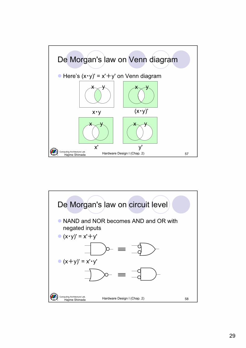
De Morgan’s law
(x・y)' = x'+y'(x+y)' = x'・y'We can insert arbitrary logical expressions into x and y
x y (x・y)' x'+y' (x+y)' x'・y'
0 0 1 1 1 1 0 1 1 1 0 0 1 0 1 1 0 0 1 1 0 0 0 0
Equal Equal
29
Hardware Design I (Chap. 2) 57Computing Architecture Lab.
Hajime Shimada
De Morgan's law on Venn diagram
Here’s (x・y)' = x'+y' on Venn diagram
x y
(x・y)'
x y
x'
x y
y'
x y
x・y
Hardware Design I (Chap. 2) 58Computing Architecture Lab.
Hajime Shimada
De Morgan's law on circuit level
NAND and NOR becomes AND and OR with negated inputs(x・y)' = x'+y'
(x+y)' = x'・y'

30
Hardware Design I (Chap. 2) 59Computing Architecture Lab.
Hajime Shimada
A practical use of De Morgan’s law on circuit level
NAND-NAND two level logic circuit= AND-OR two level logic circuit
1. Apply De Morgan’s law into latter NAND gate
2. Add involution rule
Hardware Design I (Chap. 2) 60Computing Architecture Lab.
Hajime Shimada
Generalized De Morgan’s law
Widely used when you want to negate arbitrary logical function f
F’(x1, x2,・・・, xn) = G(x1, x2,・・・, xn)
Xi Xi'+ ・
Under
e.g. ( (a・b)'・(b'・c)' )' = (a・b) + (b'・c) = a・b + b'・c
e.g. (a’b’+a’b+ab’)’ = (a+b)(a+b’)(a’+b)= aaa’+aab+ab’a’+ab’b+baa’+bab+bb’a’+bb’b= ab + ab = ab

31
Hardware Design I (Chap. 2) 61Computing Architecture Lab.
Hajime Shimada
How to create CNF?
1. Gain DNF of negated functionSum of “0” term in truth table
2. Negate function obtained in 1.a b c0 0 0 a’b’c’0 0 1 a’b’c0 1 0 a’bc’0 1 1 a’bc1 0 0 ab’c’1 0 1 ab’c1 1 0 abc’1 1 1 abc
h s t0 0 11 1 10 0 01 1 00 0 01 1 01 0 10 1 1
h’ = a’b’c’ + a’bc’ + ab’c’ + abc
h’’ = (a’b’c’ + a’bc’ + ab’c’ + abc)’
h = (a+b+c)(a+b’+c) (a’+b+c)(a’+b’+c’)
De Morgan’s law
Hardware Design I (Chap. 2) 62Computing Architecture Lab.
Hajime Shimada
Short exercise
Show CNF of following logical function
a b c d0 0 0 00 0 0 1 0 0 1 0 0 0 1 1 0 1 0 0 0 1 0 1 0 1 1 0 0 1 1 1 1 0 0 0 1 0 0 1 1 0 1 0 1 0 1 1 1 1 0 0 1 1 0 1 1 1 1 0 1 1 1 1
f 1 1 0 1 1 1 1 0 1 1 1 1 1 1 0 1

32
Hardware Design I (Chap. 2) 63Computing Architecture Lab.
Hajime Shimada
Answer
Show CNF of following logical function
a b c d0 0 0 00 0 0 1 0 0 1 0 0 0 1 1 0 1 0 0 0 1 0 1 0 1 1 0 0 1 1 1 1 0 0 0 1 0 0 1 1 0 1 0 1 0 1 1 1 1 0 0 1 1 0 1 1 1 1 0 1 1 1 1
f 1 1 0 1 1 1 1 0 1 1 1 1 1 1 0 1
f’ = a’b’cd’ + a’bcd + abcd’f = f’’ = (a’b’cd’ + a’bcd + abcd’)’= (a+b+c’+d)(a+b’+c’+d’)(a’+b’+c’+d)
Hardware Design I (Chap. 2) 64Computing Architecture Lab.
Hajime Shimada
How to translate logical expression to sum of products or product of sums
h = a’(b’c + bc) + b’c’ h’ = (a’(b’c + bc) + b’c’)’
h = a’b’c + a’bc + b’c’= a’c + b’c’
h’ = ab + ac + bc’
h’’ = h = (ab + ac + bc’)’
h = (a’+b’)(a’+c’)(b’+c)
Sum of products
Expand ExpandNegate
Negate
De Morgan’s law
Product of Sums
Note that the expansionroute is not unique

33
Hardware Design I (Chap. 2) 65Computing Architecture Lab.
Hajime Shimada
Shannon’s expansion
A technique also used for translating logical expression to sum of products notation
f(x1, x2,・・・, xn) = x1'・ f(0, x2,・・・, xn) + x1・ f(1, x2,・・・, xn)
e.g. (a’b’+a’b+ab’)’= a’((1・b’+1・b+0・b’)’)+a((0・b+0・b+1・b’)’)
= a’((b’+b)’)+a((b’)’)
= a’(0)+a(b’’) = ab
Substitute a=0 Substitute a=1
=1
Hardware Design I (Chap. 2) 66Computing Architecture Lab.
Hajime Shimada
Short exercise
Expand following function by Shannon’s expansion and translate it to sum of productsf = {(a・b)'・(b'・c)'}'

34
Hardware Design I (Chap. 2) 67Computing Architecture Lab.
Hajime Shimada
Answer
Expand following function by Shannon’s expansion and translate it to sum of productsf = {(a・b)'・(b'・c)'}'
f = a’・{(0・b)’・(b’・c)’}’ + a・{(1・b)’・(b’・c)’}’
= a’・{(b’・c)’}’ + a・{b’・(b’・c)’}’= b’・[a’・{(1・c)’}’ + a・{1・(1・c)’}’] + b・[a’・{(0・c)’}’ + a・{0・(0・c)’}’
= b’・(a’・c + a・c) + b・a= (a’ + a)・b’・c + a・b = a・b + b’・c
=1 =b’
=c =c =1=0
=1
Hardware Design I (Chap. 2) 68Computing Architecture Lab.
Hajime Shimada
Equivalence of logical function
There are equivalent logical expression in each logical function
In logical circuits design, there’s possibility that it includes same circuits (= same logical expression)
-> Redundant! (consume unnecessary silicon resources)
How to check equivalence of them?Checking on truth table is one method
The size of truth table is 2n on n-value
Cogitated algorithm or data structure are required-> Later Chap. 2

35
Hardware Design I (Chap. 2) 69Computing Architecture Lab.
Hajime Shimada
Quantity of logical function
The logical function can be represented uniquely with truth tableBut there are 22n of logical functions in n-value logical function x y Q
0 0 ?0 1 ?1 0 ?1 1 ?
There are 24 possible outputs
x y0 0 0 0 0 0 0 0 0 0 1 1 1 1 1 1 1 10 1 0 0 0 0 1 1 1 1 0 0 0 0 1 1 1 11 0 0 0 1 1 0 0 1 1 0 0 1 1 0 0 1 11 1 0 1 0 1 0 1 0 1 0 1 0 1 0 1 0 1
Hardware Design I (Chap. 2) 70Computing Architecture Lab.
Hajime Shimada
Examples of 2-input logical function
There’s possible functions which are not namedBut usually, there’s no use
AND XORx y x・y x + y (= x) (= 0) (= y) (= 1) 0 0 0 0 1 0 0 10 1 0 1 0 0 1 11 0 0 1 1 0 0 11 1 1 0 0 0 1 1

36
Hardware Design I (Chap. 2) 71Computing Architecture Lab.
Hajime Shimada
Quantity of logical function
It increases dramatically in proportion to the number of values
28 = 256 in 3-value function216 = 65536 in 4-value function232 = 4294967296 in 5-value function264 (≒ 1.8×10¹⁹) in 6-value function
Too hard to check all of them even if we use computer!
Let’s consider how to reduce number of logical functions
Hardware Design I (Chap. 2) 72Computing Architecture Lab.
Hajime Shimada
Symmetry logical function
Quantity of logical function becomes 2n+1 if the function has perfect symmetry
The outputs do not change under permutation of all variablese.g. x’1・x2・x3+x1・x’2・x3+x1・x2・x’3
Example of symmetry: f(x1,x2) = x1 + x2 (= x2 + x1)Example of not symmetry: f(x1,x2) = x’1 + x2 (≠ x’2 + x1)
The logical function is symmetry on xi and xj if outputs do not change under permutation of xi and xj


![Computer programming Lecture 4. Lecture 4: Outline Making Decisions [chap 6 – Kochan] –The if Statement –The if-else Construct –Logical Operators –Boolean](https://img.dokumen.tips/doc/110x75/56649eb35503460f94bbaad6/computer-programming-lecture-4-lecture-4-outline-making-decisions-chap-6.jpg)