Embed Size (px)
Citation preview
i
GSM BASED DISPLAY TOOLKIT
AA PPRROOJJEECCTT RREEPPOORRTT
Submitted in partial fulfillment of the requirements for the award of the
degree of
Bachelor of Technology
In
Electronics and Instrumentation Engineering
By
Rohan Mishra
Roll No: 10307006
&
Sambit Kumar Das
Roll No: 10307037
Department of Electronics and Communication Engineering
National Institute of Technology
Rourkela
2007
ii
GSM BASED DISPLAY TOOLKIT
AA PPRROOJJEECCTT RREEPPOORRTT
Submitted in partial fulfillment of the requirements for the award of the
degree of
Bachelor of Technology
In
Electronics and Instrumentation Engineering
By
Rohan Mishra (10307006)
&
Sambit Kumar Das (10307037)
Under the guidance of
PPrr ooff .. ((DDrr ..)) SS..KK .. PPAATTRRAA
Department of Electronics and Communication Engineering
National Institute of Technology
Rourkela
2007
iii
National Institute of Technology Rourkela
CERTIFICATE
This is to certify that the thesis entitled, “GSM BASED DISPLAY TOOLKIT ”
submitted by Sri Rohan Mishra and Sri Sambit Kumar Das in partial fulfillment of the
requirements for the award of Bachelor of Technology Degree in Electronics and
Instrumentation Engineering at the National Institute of Technology, Rourkela
(Deemed University) is an authentic work carried out by them under my supervision and
guidance.
To the best of my knowledge, the matter embodied in the thesis has not been submitted to
any other university / institute for the award of any Degree or Diploma.
Date: Prof. S. K. PATRA
Dept. of Electronics & Instrumentation Engg
National Institute of Technology
Rourkela - 769008
iv
ACKNOWLEDGEMENT
We place on record and warmly acknowledge the continuous encouragement,
invaluable supervision, timely suggestions and inspired guidance offered by our guide
Prof. S.K.Patra, Professor, Department of Electronics and instrumentation Engineering,
National Institute of Technology, Rourkela, in bringing this report to a successful
completion.
We are grateful to Prof. G.Panda, Head of the Department of Electronics
and instrumentation Engineering, for permitting us to make use of the facilities available
in the department to carry out the project successfully. Last but not the least we express
our sincere thanks to all of our friends who have patiently extended all sorts of help for
accomplishing this undertaking.
Finally we extend our gratefulness to Mr. Ayas Kanta Swain, Mr. Tarini
Chaitanya and all those who are directly or indirectly involved in the successful
completion of this project work.
.
Rohan Mishra
Sambit Kumar Das
v
CONTENTS
A. ABSTRACT ……………………………………………...…………………….vii B. List of Figures…………………………………….…..…………………………ix C. List of Tables ………………………………………………..…………………...x D. CHAPTERS
1. Introduction …………………………………………………………………….…1
1.1 Introduction……………………………………………………………..…….2
1.1.1 Information…………………………………………………………2
1.1.2 Information Transfer………………………………………………2
1.2 Broadcast…………………………………………………………………...…2
2. Design Overview…………………………………………………………………...4
2.1 Design on Paper…………………………………………………………….…5
3. Hardware Profile……………………………………………………….………. ..7
3.1 GSM Modem…………………………………..... ………………………...…8
3.1.1 Accessing GSM MODEM using Microsoft HyperTerminal… .....9
3.1.2 Testing of GSM MODEM………………………………………..10
3.1.3 List of Important AT Commands………………………………..14
3.2 LCD Display………………………………………………………………...15
3.2.1 Important Signals………………………………………………...17
3.2.1.1 Enable (EN)……………………………………………..17
3.2.1.2 Register Select (RS)…………………………………….17
3.2.1.3 Read/Write (R/W)………………………………………17
3.3 Microcontroller – Philips P89C51RD2BN………………………………..19
3.3.1 Description………………………………………………………...19
3.3.2 Features …………………………………………………………...20
vi
4. Interfacing……………………………………………………………………….21
4.1 Microcontroller – MODEM Interfacing…………………………… ……..22
4.1.1. DTE and DCE……………………………………………………22
4.1.2. RS-232………………………………………………………….…22
4.1.2.1 RS-232 Signals…………………………………………..23
4.1.2.2. RTS/CTS Handshaking………………………………..24
4.1.3. Specifying Baud Rate, Parity & Stop bits………………………25
4.1.3.1. DCE Baud Rates……………………………………….25
4.2 Microcontroller – LCD Interfacing…………………………………… …..25
5. Software Solvency ………………………………...…….……. ………………...25
5.1 End user Perspective……………………………………………………….28
5.2 Control flow in code………………………………………………………...31
5.2.1 Initialization……………………………………………………... 31
5.2.2. Serial transfer using TI and RI flags………………………… ..31
5.2.3. Validity Check……………………………………………………31
5.2.4 Display………………………………………………………..……31
6. Testing methodologies and Observations.………...… …………………………32
6.1 Offline testing……………………………………………………………….33
6.2 Online testing and observations……………………………………………34
7. Implementation at the Institute level……………………………………………35
7.1 Overview………………………………………………………………….…36
7.2 Proposal…………………………………………………………..…………36
8. Conclusion………………………………………………………………………..38
8.1 Conclusion…………………………………………………………………..39
8.2 Future Improvements ……………………………………………………..39
E. References……………………………………………..………………………...41
vii
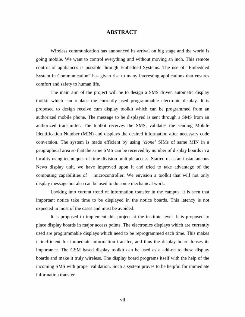
ABSTRACT
Wireless communication has announced its arrival on big stage and the world is
going mobile. We want to control everything and without moving an inch. This remote
control of appliances is possible through Embedded Systems. The use of “Embedded
System in Communication” has given rise to many interesting applications that ensures
comfort and safety to human life.
The main aim of the project will be to design a SMS driven automatic display
toolkit which can replace the currently used programmable electronic display. It is
proposed to design receive cum display toolkit which can be programmed from an
authorized mobile phone. The message to be displayed is sent through a SMS from an
authorized transmitter. The toolkit receives the SMS, validates the sending Mobile
Identification Number (MIN) and displays the desired information after necessary code
conversion. The system is made efficient by using ‘clone’ SIMs of same MIN in a
geographical area so that the same SMS can be received by number of display boards in a
locality using techniques of time division multiple access. Started of as an instantaneous
News display unit, we have improved upon it and tried to take advantage of the
computing capabilities of microcontroller. We envision a toolkit that will not only
display message but also can be used to do some mechanical work.
Looking into current trend of information transfer in the campus, it is seen that
important notice take time to be displayed in the notice boards. This latency is not
expected in most of the cases and must be avoided.
It is proposed to implement this project at the institute level. It is proposed to
place display boards in major access points. The electronics displays which are currently
used are programmable displays which need to be reprogrammed each time. This makes
it inefficient for immediate information transfer, and thus the display board looses its
importance. The GSM based display toolkit can be used as a add-on to these display
boards and make it truly wireless. The display board programs itself with the help of the
incoming SMS with proper validation. Such a system proves to be helpful for immediate
information transfer
viii
The system required for the purpose is nothing but a Microcontroller based SMS box.
The main components of the toolkit include microcontroller, GSM modem. These
components are integrated with the display board and thus incorporate the wireless
features. The GSM modem receives the SMS. The AT commands are serially transferred
to the modem through MAX232. In return the modem transmits the stored message
through the COM port. The microcontroller validates the SMS and then displays the
message in the LCD display board. Various time division multiplexing techniques have
been suggested to make the display boards functionally efficient. The microcontroller
used in this case is Philips P89C51RD2BN. Matrix Simado GDT11 is used as the GSM
modem. In the prototype model, LCD display is used for simulation purpose. While
implementation this can be replaced by actually display boards.
The results presented in the thesis support the proper functionalities and working
of the system. The timing diagram suggests the response of the modem to various AT
commands.
ix
List of Figures
1. Figure. 2.1. Design Overview
2. Figure 2.2. Commercially used display boards
3. Figure. 2.3. Schematic of the Display board commonly used
4. Figure: 3.1 Simado GDT11
5. Figure 3.2- The screenshot of MS HyperTerminal's Connection Description dialog box
6. Figure 3.3- The screenshot of MS HyperTerminal's Connect to dialog box
7. Figure 3.4- The screenshot of MS HyperTerminal's Properties dialog box
8. Figure 3.5- The screenshot of MS HyperTerminal's main window in Windows 98.
9. Figure 3.6 Philips P89C51RD2BN 1
10. Figure 4.1- Female 9 pin plug
12. Figure 4.2- Character Frame Encoding ‘m’
13. Figure 4.3- LCD Interfacing
14. Figure 4.4- Pin Configuration
15. Figure 4.5 The Experimental Setup
16 Figure 5.1. End User Perspective Flowchart
17. Figure 5.2 Operational Flowchart
18. Figure 6.1. Transmission of AT command from microcontroller
19. Figure 6.2. Reception of Response from MODEM
20. Figure 6.3. Tx and Rx lines with echo bein ON
21. Figure 6.4. Response of the modem with the new message
x
List of Tables 1. Table 3.1 Pin Configuration of LCD
2. Table 3.2 Control Codes of LCD
3. Table 4.1 RS-232 Signals

Chapter 1
INTRODUCTION
2
1.1 INTRODUCTION
Presently, the United States is the most technologically advanced country in the area of
telecommunications with about; 126 million phone lines, 7.5 million cellular phone users,
5 thousand AM radio broadcast stations, 5 thousand FM radio stations, 1 thousand
television broadcast stations, 9 thousand cable television systems, 530 million radios, 193
million television sets, 24 ocean cables, and scores of satellite facilities!
This is truly an "Information Age" and sometimes, you need to look at where we've been
in order to see the future more clearly!
1.1.1 Information
---“A message received and understood” --- Princeton
---“ Information is a term with many meanings depending on context, but is as a rule
closely related to such concepts as meaning, knowledge, instruction, communication,
representation, and mental stimulus ” --- Wikipedia
--- “ any communication or representation of knowledge such as facts, data, or opinions in
any medium or form, including textual, numerical, graphic, cartographic, narrative, or
audiovisual forms (OMB Circular A-130). ” --- Gils.net
--- “Facts, concepts, or instructions; any sort of knowledge or supposition which can be
communicated. “ --- cedar.web.cern
--- “ Is organized data that has been arranged for better comprehension or understanding.
What is one person's information can become another person's data.” --- earthlink.net
1.1.2 Information Transfer
A coordinated sequence of user and telecommunications system actions that cause
information present at a source user to become present at a destination user. Note: An
information-transfer transaction usually consists of three consecutive phases called the
access phase, the information -transfer phase, and the disengagement phase.
1.2 Broadcast
A term to describe communication where a piece of information is sent or transmitted
from one point to all other points. There is just one sender, but the information is
3
simultaneously sent to all connected receivers. In networking, a distinction is made
between broadcasting and multicasting. Broadcasting sends a message to everyone on
the network whereas multicasting sends a message to a select list of recipients.
One of the most common examples is broadcast through a cellular network
service. This serves multiple end users at different locations in a simulcast fashion.
Practically every cellular system has some kind of broadcast mechanism. This can be
used directly for distributing information to multiple mobiles, commonly, for example in
a mobile telephony system, the most important use of broadcast information is to set up
channels for one to one communication between the mobile Trans-receiver and the base
station. This is called paging. The details of the process of paging vary somewhat from
network to network, but normally we know a limited number of cells where the phone is
located (this group of cells is called a location area in the GSM system or Routing Area
in UMTS). Paging takes place by sending the broadcast message on all of those cells.
Today, interaction with digital displays is a deskbound or device-dependent
experience. However, developments in display and information sharing technologies may
enable a new form of interaction with digital media: ‘ubiquitous computing’. In
ubiquitous computing, the physical location of data and processing power is not apparent
to the user. Rather, information is made available to the user in a transparent and
contextually relevant manner. A single display device restricts the repertoire of
interactions between the user and digital media, so ubiquitous computing requires
displays wherever the user might need one – in appliances, tabletops public transport,
walls, etc.
This project aims at integrating the expansiveness of a wireless cellular network
and the ease of information transfer through the SMS with the coverage of public display
boards. It is thereby a modest effort to realize the complete potential of public display
boards in instantaneous information broadcast in swift response to events of interests.
4
Chapter 2
DESIGN
OVERVIEW

5
2.1. Design on Paper
As explained in the introduction chapter, the realization of complete potential of the
display boards and the wireless medium in information transfer is the major issue that the
following thesis of the following project deals with.
Figure 2.1. Design Overview
As we see in the above figure, there are at least three interfacing circuits, MAX-232 with
microcontroller, LCD display with microcontroller, and MAX-232 with GSM MODEM.
The display boards used commercially can be as follows:
Figure 2.2 Commercially used display boards
6
The input requirement for such kind of display boards are 120/240 VAC 50//60 Hz with
Internal circuit breaker sized per sign layout. The basic schematic of such kind of display
boards can be given as :
Figure. 2.3 Schematic of the Display board commonly used
The display boards are usually huge in size and cant be used for simulation purpose. So
LCD displays are used for testing.
It is not a hidden fact that interfacing a MODEM with a normal PC is quite easy
with the help of the AT commands sent to it from the Hyper Terminal window. But we
must take into account the fact that the MODEM requires a wired connection at one end
and wireless at the other. Dedicating a general purpose computer at each and every site of
the display boards, although makes the task a lot easier but is too expensive to be a
possibility. Hence we employ Philips P89C51RD2BN microcontroller with 64 Kb
EEROM storage memory. The complexity of coding substantially increases, but once
programmed the module works at its robust best since it is a dedicated embedded system
and not a general purpose computer. The design procedure involves identifying and
assembling all the required hardware and ensuring fail safe interfacing between all the
components. Then we have the coding process which has to take care of the delays
between two successive transmissions and most importantly the validation of the sender’s
number. The number of valid mobile numbers can be more than one. The limiting
constraint is the RAM of the microcontroller rather than the coding complexity.

7
Chapter 3
HARDWARE
PROFILE
8
3.1. GSM MODEM
A GSM modem is a wireless modem that works with a GSM wireless network. A
wireless modem behaves like a dial-up modem. The main difference between them is that
a dial-up modem sends and receives data through a fixed telephone line while a wireless
modem sends and receives data through radio waves. Like a GSM mobile phone, a GSM
modem requires a SIM card from a wireless carrier in order to operate.
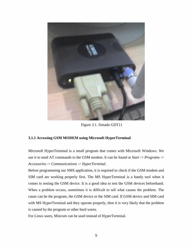
Matrix Simado GDT11 is a Fixed Cellular Terminal (FCT) for data applications.
It is a compact and portable terminal that can satisfy various data communication needs
over GSM. It can be connected to a computer with the help of a standard RS232C serial
port. Simado GDT11 offers features like Short Message Services (SMS), Data Services
(sending and receiving data files), Fax Services and Web Browsing. Remote login and
data file transfer are also supported. It is the perfect equipment for factory plants, resorts,
dams and construction sites where wired connectivity is not available or not practicable.
The Simado GDT11 is easy to set up. It finds its applications in IT companies, Banks and
Financial Institutions, Logistic Companies, Service Providers, Remote Project Sites,
Professionals, and such other business establishments.
Computers use AT commands to control modems. Both GSM modems and dial-up
modems support a common set of standard AT commands. GSM modem can be used just
like a dial-up modem. In addition to the standard AT commands, GSM modems support
an extended set of AT commands. These extended AT commands are defined in the GSM
standards. With the extended AT commands, various things can be done:
• Reading, writing and deleting SMS messages.
• Sending SMS messages.
• Monitoring the signal strength.
• Monitoring the charging status and charge level of the battery.
• Reading, writing and searching phone book entries.
The number of SMS messages that can be processed by a GSM modem per minute is
very low -- only about six to ten SMS messages per minute.
9
Figure 3.1. Simado GDT11
3.1.1 Accessing GSM MODEM using Microsoft HyperTerminal
Microsoft HyperTerminal is a small program that comes with Microsoft Windows. We
use it to send AT commands to the GSM modem. It can be found at Start -> Programs ->
Accessories -> Communications -> HyperTerminal.
Before programming our SMS application, it is required to check if the GSM modem and
SIM card are working properly first. The MS HyperTerminal is a handy tool when it
comes to testing the GSM device. It is a good idea to test the GSM devices beforehand.
When a problem occurs, sometimes it is difficult to tell what causes the problem. The
cause can be the program, the GSM device or the SIM card. If GSM device and SIM card
with MS HyperTerminal and they operate properly, then it is very likely that the problem
is caused by the program or other hard wares.
For Linux users, Mincom can be used instead of HyperTerminal.
10
3.1.2 Testing of GSM MODEM
To use MS HyperTerminal to send AT commands to the GSM modem, the following
procedure is followed
1. We put a valid SIM card into the GSM modem. We can obtain a SIM card by
subscribing to the GSM service of a wireless network operator.
2. Since in our case the modem drivers were pre installed, we need not to install any
such drivers.
3. Then we start up MS HyperTerminal by selecting Start -> Programs ->
Accessories -> Communications -> HyperTerminal.
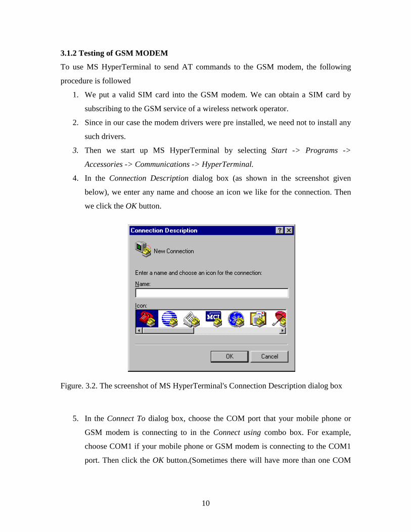
4. In the Connection Description dialog box (as shown in the screenshot given
below), we enter any name and choose an icon we like for the connection. Then
we click the OK button.
Figure. 3.2. The screenshot of MS HyperTerminal's Connection Description dialog box
5. In the Connect To dialog box, choose the COM port that your mobile phone or
GSM modem is connecting to in the Connect using combo box. For example,
choose COM1 if your mobile phone or GSM modem is connecting to the COM1
port. Then click the OK button.(Sometimes there will have more than one COM

11
port in the Connect using combo box. To know which COM port is used by your
mobile phone or GSM modem, follow the procedure below.
In Windows 98:
Go to Control Panel -> Modem. Then click the Diagnostics tab. In the list box, you
can see which COM port the mobile phone or GSM modem is connected to.
In Windows 2000 and Windows XP:
Go to Control Panel -> Phone and Modem Options. Then click the Modems tab. In
the list box, you can see which COM port the mobile phone or GSM modem is
connected to.)
Figure. 3.3. The screenshot of MS HyperTerminal's Connect to dialog box
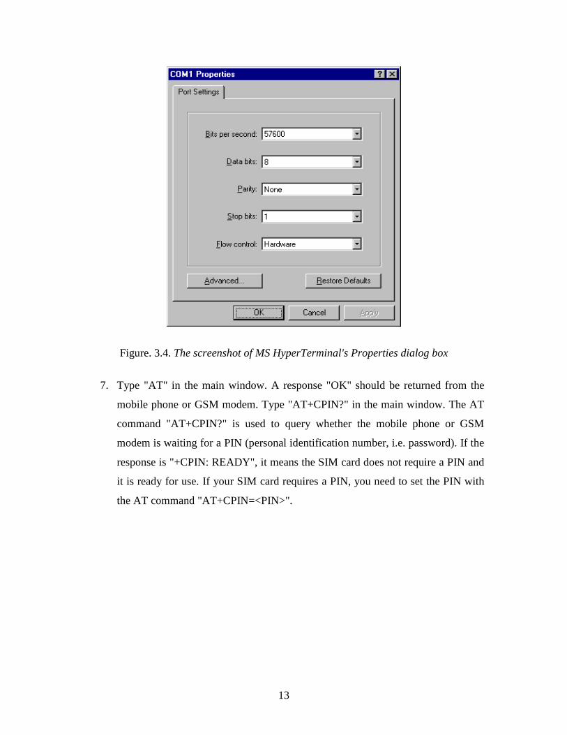
6. The Properties dialog box comes out. Enter the correct port settings for your
mobile phone or GSM modem. Then click the OK button.
(To find the correct port settings that should be used with your mobile phone or
GSM modem, one way is to consult the manual of your mobile phone or GSM

12
modem. Another way is to check the port settings used by the wireless modem
driver that you installed earlier.
To check the port settings used by the wireless modem driver on Windows 98,
follow these steps:
a. Go to Control Panel -> Modem.
b. Select your mobile phone or GSM modem in the list box.
c. Click the Properties button.
d. The Properties dialog box appears. The Maximum speeds field on the General
tab corresponds to HyperTerminal's Bits per second field. Click the Connection
tab and you can find the settings for data bits, parity and stop bits. Click the
Advanced button and you can find the setting for flow control.
To check the port settings used by the wireless modem driver on Windows 2000
and Windows XP, follow these steps:
a. Go to Control Panel -> Phone and Modem Options -> Modems tab.
b. Select your mobile phone or GSM modem in the list box.
c. Click the Properties button.
d. The Properties dialog box appears. Click the Advanced tab and then click the
Change Default Preferences button.
e. The Change Default Preferences dialog box appears. The Port speed field on
the General tab corresponds to HyperTerminal's Bits per second field. You can
also find the setting for flow control on the General tab. On the Advanced tab,
you can find the settings for data bits, parity and stop bits.)
13
Figure. 3.4. The screenshot of MS HyperTerminal's Properties dialog box
7. Type "AT" in the main window. A response "OK" should be returned from the
mobile phone or GSM modem. Type "AT+CPIN?" in the main window. The AT
command "AT+CPIN?" is used to query whether the mobile phone or GSM
modem is waiting for a PIN (personal identification number, i.e. password). If the
response is "+CPIN: READY", it means the SIM card does not require a PIN and
it is ready for use. If your SIM card requires a PIN, you need to set the PIN with
the AT command "AT+CPIN=<PIN>".

14
Figure. 3.5. The screenshot of MS HyperTerminal's main window in Windows 98.
If you get the responses above, your mobile phone or GSM modem is working properly.
You can start typing your own AT commands to control the mobile phone or GSM
modem.
2.1.3 List of Important AT Commands
After successfully testing the MODEM for its correct operational state, we need to set the
MODEM parameters like Baud rate, Echo off etc to enable easier access via a
microcontroller which we used in this project. Following is a list of the important AT
commands
Example: Changing and saving parameters
AT+IPR=2400[Enter] Transfer rate to 2400 bps
AT&W[Enter] save parameters
Send and Receive
Example: Data transfer
AT+CPIN="xxxx"[Enter] enters PIN

15
AT+CREG?[Enter] Register Network (0,1 means logged in)
ATD05111234567[Enter] Data call
Example: Send SMS with GSM modem / module
Enter SMS-Center
AT+CSCA=+491722270000[Enter] Enter SMS-Center for Vodafone Germany (T-
Mobile Germany = +491710760000)
Example: Send SMS
AT+CMGF=1[Enter]
AT+CMGS="+491711234567"[Enter]
>Please call office^Z
+CMGF=1 - set modem in text mode
Send SMS (^Z equals StrgZ). At D2 you can
send without international and local code. If you
dial with Int. and local code the transmission
from foreign networks are ensured.
Example: Receive SMS
A SMS will be stored in the GSM modem / module and being sent via RS232 to the
peripherals. The peripherals have to send commands to the GSM unit to receive SMS and
to erase SMS from the device in order to free memory.
+CMTI:"SM",x X stands for the memory number of received SMS
AT+CMGR=X[Enter] Read SMS on memory number X
AT+CMGD=X[Enter] Erase SMS on memory number X
ATZ;E[Enter] Echo OFF
ATZ;E1[Enter] Echo ON
AT+COPS?[Enter] Shows if network of SIM-card is available. 0,2,26201= D1
availiable
AT+COPS=?[Enter] Shows all available networks
3.2 LCD Display
One of the most common devices attached to an 8051 is an LCD display. Some of the
most common LCDs connected to the 8051 are 16x2 and 20x2 displays. This means 16
16
characters per line by 2 lines and 20 characters per line by 2 lines, respectively. In recent
years the LCD is finding widespread use replacing LED’s. This is due to the following
reasons
1. Declining prices
2. Ability to display numbers, characters and graphics.
3. Incorporation of a refreshing controller into the LCD.
4. Ease of programming.
Fortunately, a very popular standard exists which allows us to communicate with the vast
majority of LCDs regardless of their manufacturer. The standard is referred to as
HD44780U, which refers to the controller chip which receives data from an external
source (in this case, the 8051) and communicates directly with the LCD. The 44780
standard requires 3 control lines as well as either 4 or 8 I/O lines for the data bus. The
user may select whether the LCD is to operate with a 4-bit data bus or an 8-bit data bus.
If a 4-bit data bus is used the LCD will require a total of 7 data lines (3 control lines plus
the 4 lines for the data bus). If an 8-bit data bus is used the LCD will require a total of 11
data lines (3 control lines plus the 8 lines for the data bus).
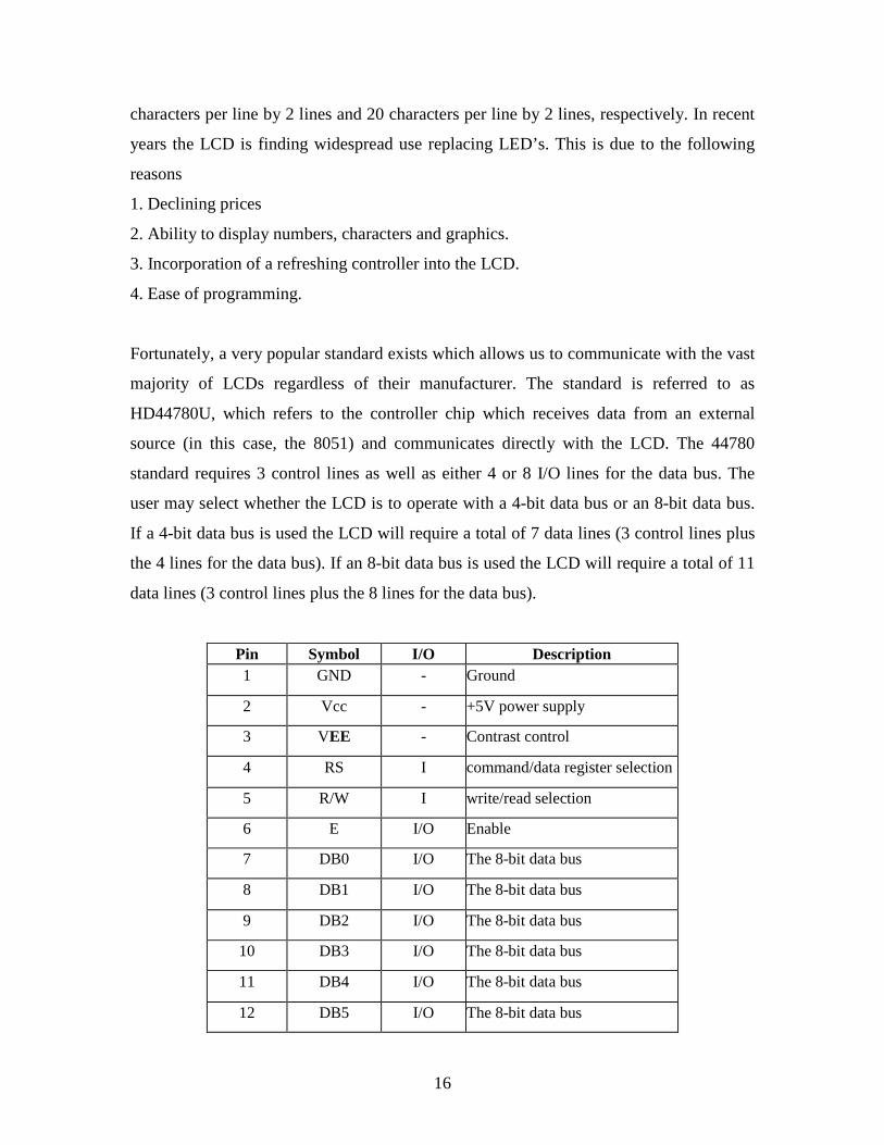
Pin Symbol I/O Description
1 GND - Ground
2 Vcc - +5V power supply
3 VEE - Contrast control
4 RS I command/data register selection
5 R/W I write/read selection
6 E I/O Enable
7 DB0 I/O The 8-bit data bus
8 DB1 I/O The 8-bit data bus
9 DB2 I/O The 8-bit data bus
10 DB3 I/O The 8-bit data bus
11 DB4 I/O The 8-bit data bus
12 DB5 I/O The 8-bit data bus
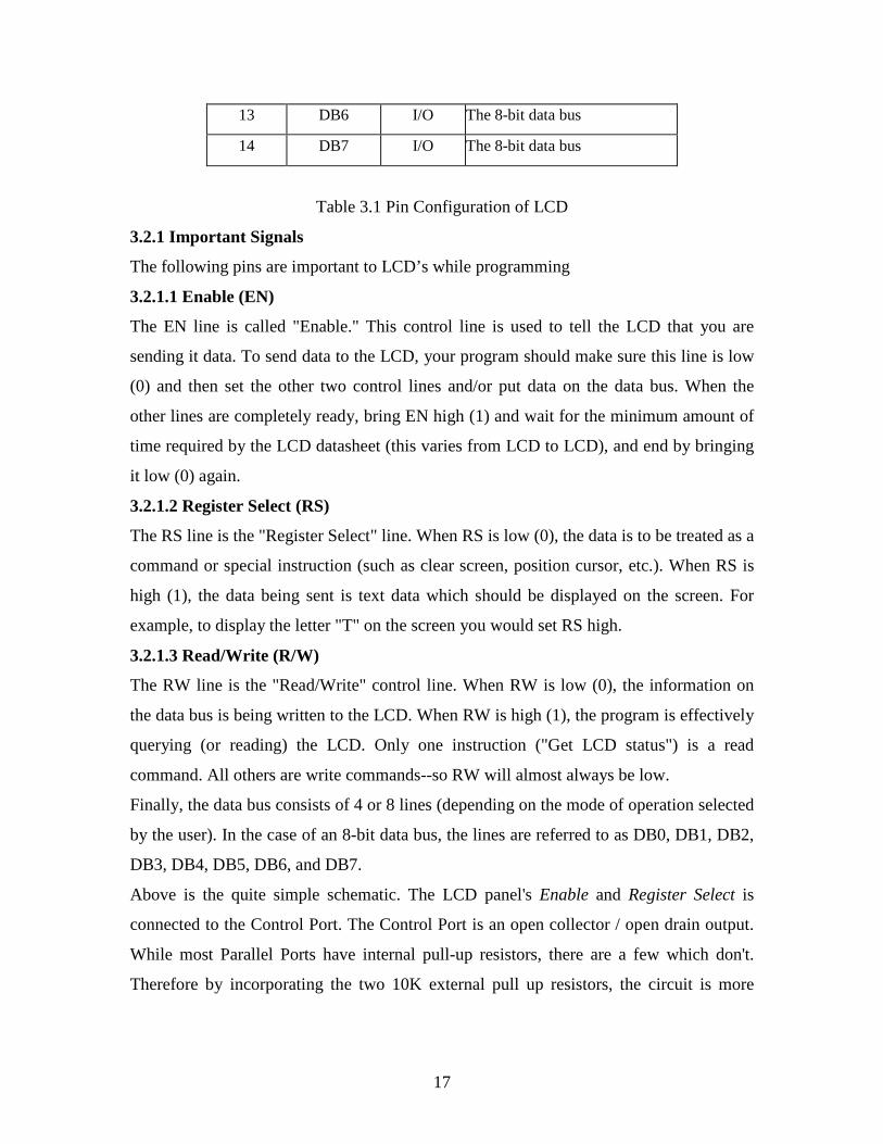
17
13 DB6 I/O The 8-bit data bus
14 DB7 I/O The 8-bit data bus
Table 3.1 Pin Configuration of LCD
3.2.1 Important Signals
The following pins are important to LCD’s while programming
3.2.1.1 Enable (EN)
The EN line is called "Enable." This control line is used to tell the LCD that you are
sending it data. To send data to the LCD, your program should make sure this line is low
(0) and then set the other two control lines and/or put data on the data bus. When the
other lines are completely ready, bring EN high (1) and wait for the minimum amount of
time required by the LCD datasheet (this varies from LCD to LCD), and end by bringing
it low (0) again.
3.2.1.2 Register Select (RS)
The RS line is the "Register Select" line. When RS is low (0), the data is to be treated as a
command or special instruction (such as clear screen, position cursor, etc.). When RS is
high (1), the data being sent is text data which should be displayed on the screen. For
example, to display the letter "T" on the screen you would set RS high.
3.2.1.3 Read/Write (R/W)
The RW line is the "Read/Write" control line. When RW is low (0), the information on
the data bus is being written to the LCD. When RW is high (1), the program is effectively
querying (or reading) the LCD. Only one instruction ("Get LCD status") is a read
command. All others are write commands--so RW will almost always be low.
Finally, the data bus consists of 4 or 8 lines (depending on the mode of operation selected
by the user). In the case of an 8-bit data bus, the lines are referred to as DB0, DB1, DB2,
DB3, DB4, DB5, DB6, and DB7.
Above is the quite simple schematic. The LCD panel's Enable and Register Select is
connected to the Control Port. The Control Port is an open collector / open drain output.
While most Parallel Ports have internal pull-up resistors, there are a few which don't.
Therefore by incorporating the two 10K external pull up resistors, the circuit is more

18
portable for a wider range of computers, some of which may have no internal pull up
resistors.
We make no effort to place the Data bus into reverse direction. Therefore we hard wire
the R/W line of the LCD panel, into write mode. This will cause no bus conflicts on the
data lines. As a result we cannot read back the LCD's internal Busy Flag which tells us if
the LCD has accepted and finished processing the last instruction. This problem is
overcome by inserting known delays into our program.
The 10k Potentiometer controls the contrast of the LCD panel. Nothing fancy here. As
with all the examples, I've left the power supply out. You can use a bench power supply
set to 5v or use a onboard +5 regulator. Remember a few de-coupling capacitors,
especially if you have trouble with the circuit working properly.
Code (hex) Command to LCD Instruction Register
1 Clear display screen
2 Return home
4 Shift cursor to left
5 Shift display right
6 Shift cursor to right
7 Shift display left
8 Display off, Cursor off
A Display off, Cursor on
C Display on, cursor off
E Display on, cursor blinking
F Display on, cursor blinking
10 Shift cursor position to left
14 Shift cursor position to right
18 Shift the entire display to the left
1C Shift the entire display to the right
80 Force cursor to beginning of 1st line
C0 Force cursor to beginning of 2nd line
38 2 lines and 5x7 matrix
Table 3.2 Control Codes of LCD
19
3.3 Microcontroller – Philips P89C51RD2BN
3.3.1 Description
The 89C51RB2/RC2/RD2 device contains a non-volatile 16kB/32kB/64kB Flash
program memory that is both parallel programmable and serial In-System and In-
Application Programmable. In-System Programming (ISP) allows the user to download
new code while the microcontroller sits in the application. In-Application Programming
(IAP) means that the microcontroller fetches new program code and reprograms itself
while in the system. This allows for remote programming over a modem link. A default
serial loader (boot loader) program in ROM allows serial In-System programming of the
Flash memory via the UART without the need for a loader in the Flash code. For In-
Application Programming, the user program erases and reprograms the Flash memory by
use of standard routines contained in ROM.
This device executes one machine cycle in 6 clock cycles, hence providing twice
the speed of a conventional 80C51. This device is a Single-Chip 8-Bit Microcontroller
manufactured in advanced CMOS process and is a derivative of the 80C51
microcontroller family. The device also has four 8-bit I/O ports, three 16-bit timer/event
counters, a multi-source, four-priority-level, nested interrupt structure, an enhanced
UART and on-chip oscillator and timing circuits. The added features of the
P89C51RB2/RC2/RD2 makes it a powerful microcontroller for applications that require
pulse width modulation, high-speed I/O and up/down counting capabilities such as motor
control.
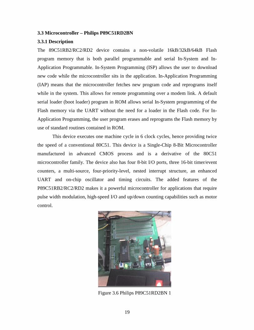
Figure 3.6 Philips P89C51RD2BN 1
20
3.3.2 Features
• 80C51 Central Processing Unit
• On-chip Flash Program Memory with In-System Programming (ISP) and In Application
Programming (IAP) capability
• Boot ROM contains low level Flash programming routines for downloading via the
UART
• Can be programmed by the end-user application (IAP)
• 6 clocks per machine cycle operation (standard)
• 12 clocks per machine cycle operation (optional)
• Speed up to 20 MHz with 6 clock cycles per machine cycle (40 MHz equivalent
performance); up to 33 MHz with 12 clocks per machine cycle
• Fully static operation
• RAM expandable externally to 64 kB
• 4 level priority interrupt
• 8 interrupt sources
• Four 8-bit I/O ports
• Full-duplex enhanced UART
–Framing error detection
– Automatic address recognition
• Power control modes
– Clock can be stopped and resumed
– Idle mode
– Power down mode
• Programmable clock out
• Second DPTR register
• Asynchronous port reset
• Low EMI (inhibit ALE)
• Programmable Counter Array (PCA)
– PWM
– Capture/compare
21
Chapter 4
INTERFACING
22
4.1 Microcontroller – MODEM Interfacing
4.1.1. DTE and DCE
The terms DTE and DCE are very common in the data communications market. DTE is
short for Data Terminal Equipment and DCE stands for Data Communications
Equipment. But what do they really mean? As the full DTE name indicates this is a piece
of device that ends a communication line, whereas the DCE provides a path for
communication.
Let's say we have a computer on which wants to communicate with the Internet
through a modem and a dial-up connection. To get to the Internet you tell your modem to
dial the number of your provider. After your modems has dialed the number, the modem
of the provider will answer your call and your will hear a lot of noise. Then it becomes
quiet and you see your login prompt or your dialing program tells you the connection is
established. Now you have a connection with the server from your provider and you can
wander the Internet. In this example you PC is a Data Terminal (DTE). The two modems
(yours and that one of your provider) are DCEs, they make the communication between
you and your provider possible. But now we have to look at the server of your provider.
Is that a DTE or DCE? The answer is a DTE. It ends the communication line between
you and the server. When you want to go from your provided server to another place it
uses another interface. So DTE and DCE are interfacing dependent. It is e.g. possible that
for your connection to the server, the server is a DTE, but that that same server is a DCE
for the equipment that it is attached to on the rest of the Net.
4.1.2. RS-232
In telecommunications, RS-232 is a standard for serial binary data signals connecting
between a DTE (Data terminal equipment) and a DCE (Data Circuit-terminating
Equipment). It is commonly used in computer serial ports. In RS-232, data is sent as a
time-series of bits. Both synchronous and asynchronous transmissions are supported by
the standard. In addition to the data circuits, the standard defines a number of control
circuits used to manage the connection between the DTE and DCE. Each data or control
circuit only operates in one direction that is, signaling from a DTE to the attached DCE
23
or the reverse. Since transmit data and receive data are separate circuits, the interface can
operate in a full duplex manner, supporting concurrent data flow in both directions. The
standard does not define character framing within the data stream, or character encoding.
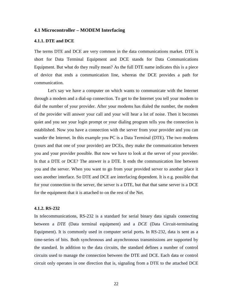
Figure 4.1 Female 9 pin plug
Function Signal PIN DTE DCE
TxD 3 Output Input Data
RxD 2 Input Output
RTS 7 Output Input
CTS 8 Input Output
DSR 6 Input Output
DCD 1 Input Output
Handshake
STR 4 Output Input
Common Com 5 -- --
Other RI 9 Output Input
Table 4.1 RS-232 Signals
4.1.2.1 RS-232 Signals
Transmitted Data (TxD)
Data sent from DTE to DCE.
Received Data (RxD)
Data sent from DCE to DTE.
Request To Send (RTS)
Asserted (set to 0) by DTE to prepare DCE to receive data. This may require
action on the part of the DCE, e.g. transmitting a carrier or reversing the direction
of a half-duplex line.
24
Clear To Send (CTS)
Asserted by DCE to acknowledge RTS and allow DTE to transmit.
Data Terminal Ready (DTR)
Asserted by DTE to indicate that it is ready to be connected. If the DCE is a
modem, it should go "off hook" when it receives this signal. If this signal is de-
asserted, the modem should respond by immediately hanging up.
Data Set Ready (DSR)
Asserted by DCE to indicate an active connection. If DCE is not a modem (e.g. a
null-modem cable or other equipment), this signal should be permanently asserted
(set to 0), possibly by a jumper to another signal.
Carrier Detect (CD)
Asserted by DCE when a connection has been established with remote equipment.
Ring Indicator (RI)
Asserted by DCE when it detects a ring signal from the telephone line.
4.1.2.2. RTS/CTS Handshaking
The standard RS-232 use of the RTS and CTS lines is asymmetrical. The DTE asserts
RTS to indicate a desire to transmit and the DCE asserts CTS in response to grant
permission. This allows for half-duplex modems that disable their transmitters when not
required, and must transmit a synchronization preamble to the receiver when they are re-
enabled. There is no way for the DTE to indicate that it is unable to accept data from the
DCE. A non-standard symmetrical alternative is widely used: CTS indicates permission
from the DCE for the DTE to transmit, and RTS indicates permission from the DTE for
the DCE to transmit. The "request to transmit" is implicit and continuous. The standard
defines RTS/CTS as the signaling protocol for flow control for data transmitted from
DTE to DCE. The standard has no provision for flow control in the other direction. In
practice, most hardware seems to have repurposed the RTS signal for this function. A
minimal “3-wire” RS-232 connection consisting only of transmits data, receives data and
ground, and is commonly used when the full facilities of RS-232 are not required. When
only flow control is required, the RTS and CTS lines are added in a 5-wire version. In our
25
case it was imperative that we connected the RTS line of the microcontroller (DTE) to
ground to enable receipt of bit streams from the modem.
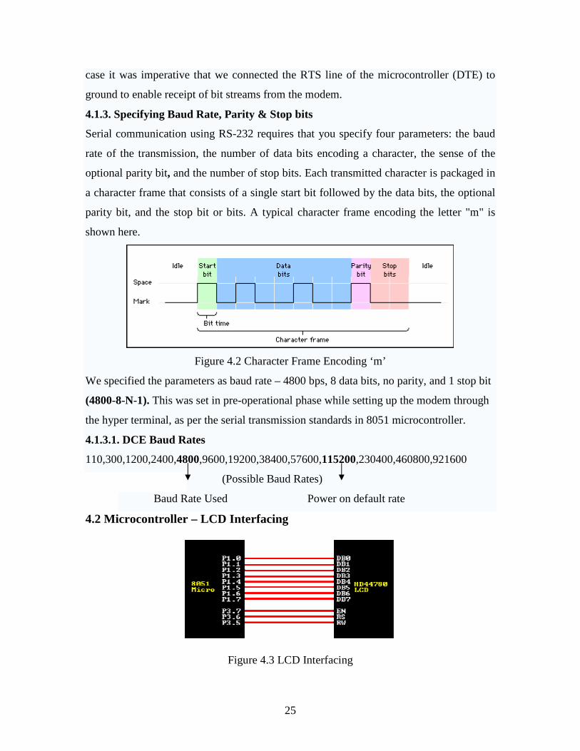
4.1.3. Specifying Baud Rate, Parity & Stop bits
Serial communication using RS-232 requires that you specify four parameters: the baud
rate of the transmission, the number of data bits encoding a character, the sense of the
optional parity bit, and the number of stop bits. Each transmitted character is packaged in
a character frame that consists of a single start bit followed by the data bits, the optional
parity bit, and the stop bit or bits. A typical character frame encoding the letter "m" is
shown here.
Figure 4.2 Character Frame Encoding ‘m’
We specified the parameters as baud rate – 4800 bps, 8 data bits, no parity, and 1 stop bit
(4800-8-N-1). This was set in pre-operational phase while setting up the modem through
the hyper terminal, as per the serial transmission standards in 8051 microcontroller.
4.1.3.1. DCE Baud Rates
110,300,1200,2400,4800,9600,19200,38400,57600,115200,230400,460800,921600
(Possible Baud Rates)
Baud Rate Used Power on default rate
4.2 Microcontroller – LCD Interfacing
Figure 4.3 LCD Interfacing

26
Figure 4.4 Pin Configuration
Above is the quite simple schematic. The LCD panel’s Enable and Register Select is
connected to the Control Port. The Control Port is an open collector / open drain output.
While most Parallel Ports have internal pull-up resistors, there are a few which don’t.
Therefore by incorporating the two 10K external pull up resistors, the circuit is more
portable for a wider range of computers, some of which may have no internal pull up
resistors.
We make no effort to place the Data bus into reverse direction. Therefore we hard wire
the R/W line of the LCD panel, into write mode. This will cause no bus conflicts on the
data lines. As a result we cannot read back the LCD’s internal Busy Flag which tells us if
the LCD has accepted and finished processing the last instruction. This problem is
overcome by inserting known delays into our program.
The 10k Potentiometer controls the contrast of the LCD panel. Nothing fancy here. As
with all the examples, I’ve left the power supply out. You can use a bench power supply
set to 5v or use a onboard +5 regulator.
The user may select whether the LCD is to operate with a 4-bit data bus or an 8-
bit data bus. If a 4-bit data bus is used, the LCD will require a total of 7 data lines. If an
8-bit data bus is used, the LCD will require a total of 11 data lines. The three control lines
are EN, RS, and RW. Note that the EN line must be raised/lowered before/after each
instruction sent to the LCD regardless of whether that instruction is read or write text or
instruction. In short, you must always manipulate EN when communicating with the
LCD. EN is the LCD’s way of knowing that you are talking to it. If you don’t raise/lower
EN, the LCD doesn’t know you’re talking to it on the other lines.
27
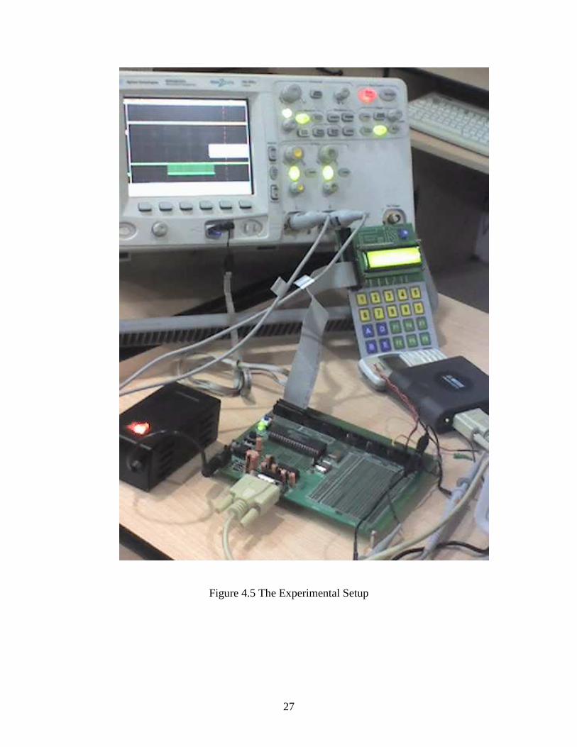
Figure 4.5 The Experimental Setup

28
Chapter 5
SOFTWARE
SOLVENCY
29
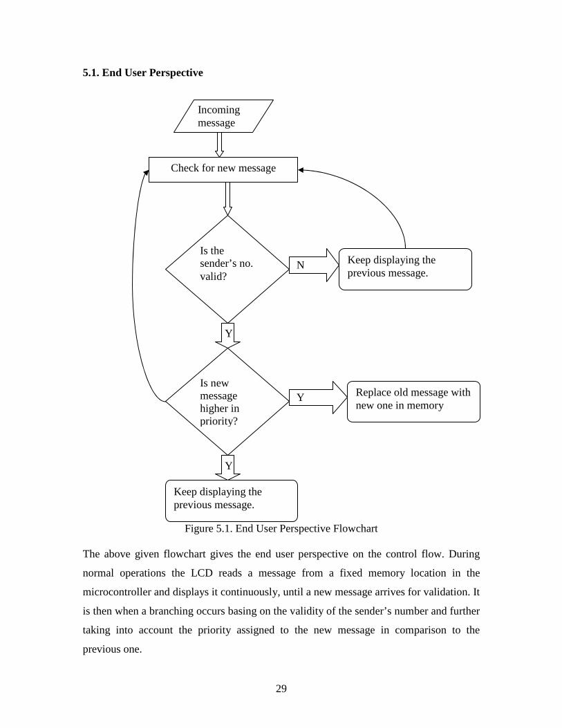
5.1. End User Perspective
Figure 5.1. End User Perspective Flowchart
The above given flowchart gives the end user perspective on the control flow. During
normal operations the LCD reads a message from a fixed memory location in the
microcontroller and displays it continuously, until a new message arrives for validation. It
is then when a branching occurs basing on the validity of the sender’s number and further
taking into account the priority assigned to the new message in comparison to the
previous one.
Is the sender’s no. valid?
Check for new message
Keep displaying the previous message.
Incoming message
Replace old message with new one in memory
N
Y
Is new message higher in priority?
Y
Keep displaying the previous message.
Y

30
Figure 5.2 Operational Flowchart

31
5.2. Control Flow in Code
5.2.1. Initializations
The baud rate of the modem was set to be 4800 bps using the command
AT+IPR=4800.The ECHO from the modem was turned off using the command
ATE/ATE0 at the hyper terminal. For serial transmission and reception to be possible
both the DTE and DCE should have same operational baud rates. Hence to set the
microcontroller at a baud rate of 4800bps, we set terminal count of Timer 1 at 0FFh
(clock frequency = 1.8432). The TCON and SCON registers were set accordingly.
5.2.2. Serial transfer using TI and RI flags
After setting the baud rates of the two devices both the devices are now ready to transmit
and receive data in form of characters. Transmission is done when TI flag is set and
similarly data is known to be received when the Rx flag is set. The microcontroller then
sends an AT command to the modem in form of string of characters serially just when the
TI flag is set. After reception of a character in the SBUF register of the microcontroller
(response of MODEM with the read message in its default format or ERROR message or
OK message), the RI flag is set and the received character is moved into the physical
memory of the microcontroller.
5.2.3. Validity Check
After serially receiving the characters the code then checks for start of the sender’s
number and then compares the number character by character with the valid number pre
stored in the memory. Since we are employing just one valid number, we are able to do
the validation process dynamically i.e. without storing the new message in another
location in the memory. For more than one valid numbers we would require more
memory locations to first store the complete (valid/invalid) message in the memory and
then perform the comparison procedure.
5.2.4 Display
After validity check the control flow goes into the LCD program module to display the
valid message stored in the memory. In case of multiple valid numbers all invalid stored
messages are deleted by proper branching in the code to the “delete-message” module.
32
Chapter 6
TESTING
METHODOLOGIES AND
OBSERVATIONS
33
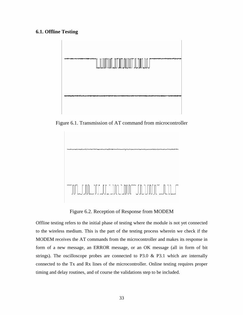
6.1. Offline Testing
Figure 6.1. Transmission of AT command from microcontroller
Figure 6.2. Reception of Response from MODEM
Offline testing refers to the initial phase of testing where the module is not yet connected
to the wireless medium. This is the part of the testing process wherein we check if the
MODEM receives the AT commands from the microcontroller and makes its response in
form of a new message, an ERROR message, or an OK message (all in form of bit
strings). The oscilloscope probes are connected to P3.0 & P3.1 which are internally
connected to the Tx and Rx lines of the microcontroller. Online testing requires proper
timing and delay routines, and of course the validations step to be included.

34
6.2. Online testing & Observations
After inclusion of the validation module in the program code, we test the module in
online mode. In this prototype we used only one valid number. With more memory
available three or four valid numbers can be included. When a message is sent to number
carried by the SIM of the MODEM, the validation module of the program checks
character by character the sender’s number with the number stored in the memory as the
valid or authentic number (in our case the only valid number).With the same probe
connections as in the case of offline testing, we then look for signals on the Tx and Rx
lines. What we see below on the left are the signals on these lines with the ECHO being
ON(ATE1). The corresponding picture on the right depicts the modem response after
about 460 ms (variable as per message length :D) delay with the new message.
Figure 6.3. Tx and Rx lines with Figure 6.4. Response of the modem with ECHO being ON. the new message

35
Chapter 7
IMPLEMENTATION
AT INSTITUTE LEVEL
36
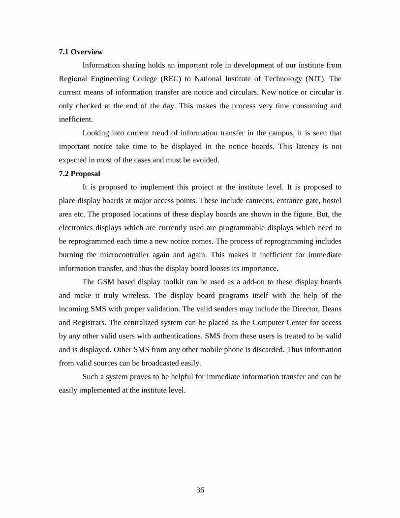
7.1 Overview
Information sharing holds an important role in development of our institute from
Regional Engineering College (REC) to National Institute of Technology (NIT). The
current means of information transfer are notice and circulars. New notice or circular is
only checked at the end of the day. This makes the process very time consuming and
inefficient.
Looking into current trend of information transfer in the campus, it is seen that
important notice take time to be displayed in the notice boards. This latency is not
expected in most of the cases and must be avoided.
7.2 Proposal
It is proposed to implement this project at the institute level. It is proposed to
place display boards at major access points. These include canteens, entrance gate, hostel
area etc. The proposed locations of these display boards are shown in the figure. But, the
electronics displays which are currently used are programmable displays which need to
be reprogrammed each time a new notice comes. The process of reprogramming includes
burning the microcontroller again and again. This makes it inefficient for immediate
information transfer, and thus the display board looses its importance.
The GSM based display toolkit can be used as a add-on to these display boards
and make it truly wireless. The display board programs itself with the help of the
incoming SMS with proper validation. The valid senders may include the Director, Deans
and Registrars. The centralized system can be placed as the Computer Center for access
by any other valid users with authentications. SMS from these users is treated to be valid
and is displayed. Other SMS from any other mobile phone is discarded. Thus information
from valid sources can be broadcasted easily.
Such a system proves to be helpful for immediate information transfer and can be
easily implemented at the institute level.
37
Figure 7.1 The Proposed location of display boards
(Blue Squares –Display Board, Yellow Circles – Authenticated Sender)

38
Chapter 8
CONCLUSION
39
8.1 Conclusion:
The prototype of the GSM based display toolkit was efficiently designed. This prototype
has facilities to be integrated with a display board thus making it truly mobile. The toolkit
accepts the SMS, stores it, validates it and then displays it in the LCD module. The SMS
is deleted from the SIM each time it is read, thus making room for the next SMS. The
major constraints incorporated are the use of ‘*’ as the termination character of the SMS
and the display of one SMS as a time. These limitations can be removed by the use of
higher end microcontrollers and extended RAM.
The prototype can be implemented using commercial display boards. In this case,
it can solve the problem of instant information transfer in the campus.
8.2 Future Improvements
The use of microcontroller in place of a general purpose computer allows us to theorize
on many further improvements on this project prototype. Temperature display during
periods wherein no message buffers are empty is one such theoretical improvement that
is very possible. The ideal state of the microcontroller is when the indices or storage
space in the SIM memory are empty and no new message is there to display. With proper
use of interrupt routines the incoming message acts as an interrupt, the temperature
display is halted and the control flow jumps over to the specific interrupt service routine
which first validates the sender’s number and then displays the information field. Another
very interesting and significant improvement would be to accommodate multiple receiver
MODEMS at the different positions in a geographical area carrying duplicate SIM cards.
With the help of principles of TDMA technique, we can choose to simulcast and /or
broadcast important notifications. After a display board receives the valid message
through the MODEM and displays it, it withdraws its identification from the network &
synchronously another nearby MODEM signs itself into the network and starts to receive
the message. The message is broadcast by the mobile switching center for a continuous
time period during which as many possible display board MODEMS “catch” the message
and display it as per the constraint of validation.
Multilingual display can be another added variation of the project. The display
boards are one of the single most important media for information transfer to the
maximum number of end users. This feature can be added by programming the
40
microcontroller to use different encoding decoding schemes in different areas as per the
local language. This will ensure the increase in the number of informed users. Graphical
display can also be considered as a long term but achievable and target able output. MMS
technology along with relatively high end microcontrollers to carry on the tasks of
graphics encoding and decoding along with a more expansive bank of usable memory can
make this task a walk in the park.

41
REFERENCES
Literature
8051 Microcontroller and Embedded Systems – Muhammad A. Mazidi
MATRIX SIMADO GDT11 GSM MODEM Manual
Links
MAX – 232 data sheet from Texas Instruments
http://www.datasheetcatalog.com
http://matrixtelesol.com
http://www.8052.com
www.wikipedia.org
www.keil.com/forum/docs
http://www.alldatasheet.co.kr/datasheet-pdf/pdf_kor/PHILIPS/P89C51RD2BN/01.html
www.embeddedrelated.com
www.howstuffworks.com