Embed Size (px)
Citation preview

Growth and characterization of magnetoelectric
YMnO3 epitaxial thin films
PhD Thesis
Xavier Martí Rovirosa
Supervisors: Dr. F. Sánchez and Prof. J. Fontcuberta
Departament de Física, Facultat de Ciències
Universitat Autònoma de Barcelona
December 2009


Florencio Sánchez Barrera i Josep Fontcuberta i Griñó, ambdós
investigadors del CSIC a l’Institut de Ciència de Materials de Barcelona,
CERTIFIQUEN
Que Xavier Martí Rovirosa, llicenciat en Ciències Físiques per la
Universitat de Barcelona, ha dut a terme sota la nostra direcció el treball
que porta per títol “Growth and characterization of magnetoelectric
YMnO3 epitaxial thin films”, i queda recollit en aquesta memòria per optar
al grau de Doctor en Ciència de Materials.
I perquè així consti, signen el present certificat.
Dr. Florencio Sánchez Barrera Prof. Josep Fontcuberta i Griñó
Bellaterra,16 de desembre de 2009


To Xavier Ruiz and Francesc Roig
A tutte le avventure intorno al λago


i
Abstract Multiferroic materials display simultaneously more than one switchable
ferroic order. In the case of simultaneous ferroelectricity and ferromagnetism,
multiferroics have been proposed to allow building a new generation of devices,
eventually overcoming critical limitations in technology. For instance, the
eventual coupling among both ferroic orders would lead to spin filters controlled
by an electric field or contact-less control of electric polarization using magnetic
fields. It follows that an essential point for the optimal exploitation of such
materials is that the ferroic orders are coupled.
Rare earth manganites present an excellent frame to study such coupling
from two very different perspectives. As a function of the rare earth ionic radius
their stable phase is either hexagonal or the orthorhombic. Of relevance here is
that in both phases a coupling between the electrical and magnetic properties
would exist. On one hand, in the hexagonal rare earth manganites (ferroelectric
below Tc ~ 900 K and antiferromagnetic below TN ~ 90 K) the domain walls of
both ferroic orders are coupled. On the other hand, in the orthorhombic phase
(antiferromagnetic below TN ~ 40 K) theoretical works indicate that the magnetic
interactions lead to small atomic displacements and ferroelectricity.
Both phases are investigated in the present thesis using YMnO3 thin films.
Then, the thesis is structured in two different blocks.
In the first block the orthorhombic phase is covered. Epitaxial thin films
were grown by pulsed laser deposition with the aim of tuning the magnetic
topology (angles and distances) via the epitaxial strain and, as a consequence,
control the magnetic and dielectric properties as well as its eventual coupling.
Through the deposition conditions, the sample thickness, partial cationic
substitutions and by annealing of the samples, the epitaxial strain in the films is
controlled. It turns out that the magnetic properties display a critical dependence
on the epitaxial strain. Indeed, an increased ferromagnetic behaviour appears with
increasing strain. The magnetic anisotropy of the resulting structure indicates that

ii
ferromagnetism arises from a strain-tuned canted spin structure. Finally, it is
shown how the modification of the epitaxial strain resounds on the dielectric
properties and the magnetoelectric coupling.
In the second block, hexagonal YMnO3 epitaxial films are sandwiched
between bottom Pt and top permalloy electrodes. Bottom epitaxial Pt
(111)-oriented buffers will be required for the subsequent growth of (0001)-
oriented YMnO3, that is, with the ferroelectric polar axis oriented perpendicular to
the electrodes. The permalloy electrode (ferromagnetic) is expected to couple to
the YMnO3 (antiferromagnetic) via exchange bias. The objective of this block is
to exploit the coupling of the ferroelectric and antiferromagnetic domain walls in
hexagonal YMnO3 to modify the exchange bias via an electrical field applied
between the Pt and Py electrodes. The block covers a detailed characterization of
the heterostructure. Exchange bias is demonstrated by magnetometry and angular
dependent magnetoresistance. In a second step, magnetization of the permalloy
electrode is modified using electrical pulses and dc biasing of the YMnO3 layer. It
is concluded that the electric field effects modify the exchange bias.
iii
Resumen Los materiales multiferroicos presentan simultáneamente más de un orden
ferroico conmutable. En el caso ferroelectricidad y ferromagnetismo simultáneos,
los materiales multiferroicos han sido propuestos para tomar un rol fundamental
en una nueva generación de dispositivos, incluso apuntando como solución para
superar las limitaciones tecnológicas actuales. Por ejemplo, un eventual
acoplamiento entre la ferroelectricidad y el ferromagnetismo podría permitir la
fabricación de uniones túnel controladas eléctricamente o, también, a un control
de la polarización eléctrica mediante campos magnéticos sin la necesidad de
contactos eléctricos. Resulta evidente que un punto esencial de cara a la
explotación de tales materiales es que exista el acoplamiento entre tales órdenes
ferroicos.
Las manganitas de tierras raras presentan un marco excepcional para el
estudio de tal acoplamiento desde dos perspectivas diferentes. En función del
radio iónico de la tierra rara, la fase estable es hexagonal u ortorrómbica. El
interés reside en que en ambas fases existe un acoplamiento entre las propiedades
eléctricas y magnéticas. Por un lado, en las manganitas hexagonales
(ferroeléctricas debajo de Tc ~ 900 K y antiferromagnéticas debajo de TN ~ 90 K)
las paredes de dominio de ambos órdenes están acopladas. Por otro lado, en la
fase ortorrómbica (antiferromagnética debajo TN ~ 40 K) las interacciones
magnéticas dan lugar a pequeños desplazamientos atómicos que crean dipolos
eléctricos y dan lugar a ferroelectricidad.
Ambas fases son investigadas en la presente tesis doctoral usando capas
delgadas de manganita de itrio (YMnO3). La tesis queda estructurada en dos
bloques diferenciados.
En primer lugar se trata la fase ortorrómbica. Capas delgadas epitaxiales
han sido crecidas mediante ablación láser pulsada con la intención de modificar la
topología magnética (ángulos y distancias) mediante la tensión epitaxial y, a su
vez, controlar las propiedades magnéticas y dieléctricas así como su evenutal

iv
acoplamiento. Mediante las condiciones de depósito, espesor de las capas,
substitución parcial catiónica y recocidos posteriores, la tensión epitaxial resulta
controlada. Las propiedades magnéticas presentan una marcada dependencia con
la tensión epitaxial. Efectivamente, aparece una creciente componente
ferromagnética a medida que aumenta la tensión epitaxial. La anisotropía
magnética confirma que el origen del ferromagnetismo es una inclinación de los
momentos magnéticos. Finalmente, se muestra como dicha tensión epitaxial
implica cambios en las propiedades dieléctricas y el acoplamiento
magnetoeléctrico.
En el segundo bloque, capas delgadas de manganita de itrio hexagonal se
sitúan entre un eléctrodo inferior de platino y uno superior de permalloy. Un
eléctrodo de platino inferior con la orientación fuera del plano (111) es necesario
para obtener capas delgadas de YMnO3 hexagonal con la textura (0001), es decir,
con el eje de polarización ferroeléctrica orientado perpendicularmente a los
eléctrodos. Se espera que el eléctrodo superior de permalloy se acopla por
intercambio de canje (exchange bias) con la capa antiferromagnética de YMnO3.
El objetivo de este bloque es utilizar el acoplamiento de paredes de dominio
reportado en YMnO3 hexagonal para modificar el intercambio de canje mediante
un campo eléctrico aplicado entre los eléctrodos de permalloy y platino. Se
muestra una caracterización detallada de la heteroestructura Py/YMnO3/Pt. El
campo de canje es observado por magnetometría y medidas de
magnetorresistencia anisótropa. En un segundo paso, la magnetización del
eléctrodo superior se modifica mediante la aplicación de campos eléctricos
(pulsados o continuos). Se concluye que el campo eléctrico modifica el campo de
intercambio.

v
Resum Els materials multiferroics presenten simultàniament més d’un ordre
ferroic conmutable. En el cas de ferromagnetisme i ferroelectricitat simultànies,
els materials multiferroics han estat proposats per desenvolupar un rol fonamental
en una nova generació de dispositius, fins i tot apuntant com a solució per superar
les limitacions tecnològiques actuals. Per exemple, un eventual acoblament entre
ferroelectricitat i ferromagnetisme permetria fabricar unions túnel controlades
elèctricament o, també, a un control de la polarització elèctrica mitjançant camps
magnètics sense la necessitat de contactes. Resulta evident que un punt essencial
de cara a l’explotació de tals materials és que existeixi l’acoblament entre tals
ordres ferroics.
Les manganites de terres rares presenten un marc excepcional per a
l’estudi de tal acoblament des de dues perspectives ben diferents. En funció del
radi iònic de la terra rara, la fase estable és hexagonal o ortoròmbica. El interès
rau en que en ambdues fases existeix un acoblament entre les propietats
elèctriques i magnètiques. Per un costat, en les manganites hexagonals
(ferroelèctriques per sota de Tc ~ 900 K i antiferromagnètiques per sota de TN ~
90 K) les parets de domini d’ambdós ordres estan acoblades. Per altra banda, en la
fase ortoròmbica (antiferromagnètica per sota de TN ~ 40 K) les interaccions
magnètiques donen lloc a petits desplaçaments atòmics que creen dipols elèctrics.
Ambdues fases són investigades en la present tesis usant capes primes de
manganita d’itri (YMnO3). La tesi queda estructurada en dos blocs diferenciats.
En el primer bloc es tracta la fase ortoròmbica. Capes primes epitaxials
han estat crescudes per ablació làser polsada amb la intenció de modificar la
topologia magnètica (angles i distàncies) mitjançant la tensió epitaxial i, de retruc,
controlar les propietats magnètiques i dielèctriques així com llur eventual
acoblament. Per mitjà de les condicions de dipòsit, gruix de les capes, substitució
parcial catiònica i recuits posteriors, la tensió epitaxial resulta controlada. Les
propietats magnètiques presenten una dependència marcada amb la tensió
vi
epitaxial. De fet, apareix una creixent component ferromagnètica a mesura que
s’incrementa la tensió epitaxial. L’anisotropia magnètica confirma que l’origen
del ferromagnetisme és una inclinació dels moments magnètics. Finalment, es
mostra com la tensió epitaxial regula les propietats dielèctriques i l’acoblament
magnetoelèctric.
En el segon bloc, capes primes de manganita d’itri hexagonal es situen
entre un elèctrode inferior de platí i un superior de permalloy. Un elèctrode
inferior de platí amb la orientació fora del pla (111) és necessari per tal d’obtenir,
en un pas posterior, el creixement amb la textura (0001) de la manganita d’itri.
D’aquesta forma, l’eix ferroelèctric de la manganita d’itri, [0001], queda orientat
perpendicularment als elèctrodes. S’espera també que la capa prima superior de
permalloy quedi acoblada per camp d’intercanvi (exchange bias) amb la capa de
manganita d’itri inferior. L’objectiu d’aquest bloc és utilitzar l’acoblament
reportat entre parets de domini ferroelèctriques i antiferromagnètiques en YMnO3
per tal de controlar el camp d’intercanvi mitjançant un camp elèctric aplicat entre
els elèctrodes. En el segon bloc es mostra una caracterització detallada de la
heteroestructura Py/YMnO3/Pt. El camp d’intercanvi és observat amb
magnetometria així com també per magnetoresistència anisòtropa. En un segon
pas, la magnetització de l’elèctrode superior es modificada per l’aplicació de
camps elèctrics (polsats o continus). Es conclou que el camp elèctric modifica el
camp d’intercanvi.

vii
Acknowledgements
Scientific acknoledgements
En primer lloc, al Prof. Josep Fontcuberta, codirector de la tesi doctoral,
per donar-me la oportunitat d’entrar en el món de la recerca científica i guiar-me
amb increïble creativitat. Vull agrair el treball i suport diari del Dr. Florencio
Sánchez, codirector de la tesi doctoral, que no ha deixat escapar-se mai ni un
detall.
Tot seguit, vull remarcar els noms Prof. Vassil Skumryev i Prof. Vladimir
Laukhin, investigadors ICREA, pel seu vital treball en la caracterització funcional
de mostres.
Vull agrair la disposició del meu tutor de la Universitat Autònoma de
Barcelona, Dr. Javier Rodríguez Viejo.
Seguidament, vull agrair a Prof. Manuel Varela per la seva col·laboració
en el creixement de capes fines amb ablació làser a la Universitat de Barcelona.
L’agraïment el vull fer extensiu a tot el departament de Física Aplicada i Òptica,
en especial, al Dr. Cèsar Ferrater per la seva ajuda en la caracterització estructural
de les mostres.
A Dr. Jean-François Bobo i Dra. Ulrike Lüders del CNRS pel seu suport
en el creixement dels elèctrodes de platí i permalloy. La col·laboració amb ells ha
estat eficient i crucial per al treball en YMnO3 hexagonal.
A Dr. Riccardo Bertaco i Dr. Andrea Cattoni del Politecnico di Milano pel
seu treball amb XPS sobre les mostres ortoròmbiques.
Al Prof. Enric Bertran i Miquel Rubio, pel llarg treball d’optimització en
els dipòsits de permalloy realitzats a la Universitat de Barcelona per reproduir i
millorar els resultats obtinguts amb el permalloy del CNRS.
Una menció especial per Dra. Lourdes Fàbrega i Ignasi Fina del ICMAB
per les mesures dielèctriques de les mostres ortoròmbiques.
Igualment, agrair al Dr. R. Bachelet la realització de capes primes sobre

viii
STO(110), mostres hexagonals sobre Pt(111) i el treball de l’optimització del
elèctrode inferior de Platí. Aquest treball ha estat realitzat amb el suport del Dr. J.
Santiso del CIN2.
Vull agrair la caracterització estructural mitjançant microscòpia
electrònica de transmissió realitzada per Sònia Estradé, Dr. Jordi Arbiol i Dra.
Francesca Peiró del Departament d’Electrònica de la Universitat de Barcelona.
Voldria mencionar el suport del Dr. Pep Bassas i Dr. Xavier Alcover del Servei de
Raigs-X de la Universitat de Barcelona i Dr. Pierre Baules del servei de difracció
del centre CEMES (Toulouse). Al Dr. Lorenzo Calvo dels Serveis Científico-
Tècnics pel suport en les mesures realitzades d’XPS. Al Dr. Ángel Perez i la
Maite del servei de microscòpia de forces atòmiques; al José Manuel i Bernat del
servei de mesures magnètiques i de transport; al Xavi, al Joan i a l’Anna Crespi
del servei de Raigs-X del ICMAB; a l’Anna Esther en la síntesi de targets de
PLD.
Financial acknowledgement
Financial support by Spanish Government (projects NAN2004-9094-C03
and MAT2005-5656-C04, and the I3P-2006 grant) and by the EU (project
MaCoMuFi (FP6-03321) and FEDER) are acknowledged.
Personal acknowledgements
Vull agrair el suport en la meva pròxima etapa de recerca a Jordi Rius,
Jose Santiso, David Hrabovsky, Vassil Skumryev i els meus directors de tesi.
Un especial reconeixement per TOTS els amics del ICMAB.

ix
Table of contents
1. Motivation, objectives and outline of the thesis............................................ 1
1.1 Objectives of the thesis.............................................................................................. 4 1.2 Outline of the thesis ................................................................................................... 5
2. Introduction ..................................................................................................... 9
2.1 Introduction to RMnO3: structure and phase diagram ............................................... 9 2.2 Introduction to orthorhombic RMnO3 ..................................................................... 13 2.3 Introduction to hexagonal RMnO3........................................................................... 19 2.4 State-of-the-art in epitaxial YMnO3 thin films ........................................................ 23 2.5 Exchange bias .......................................................................................................... 29 2.6 Anisotropic magnetoresistance with exchange bias ................................................ 34
3. Experimental techniques .............................................................................. 39
3.1 Growth techniques................................................................................................... 39 3.2 Characterization techniques..................................................................................... 43
4. Orthorhombic YMnO3: Ferromagnetism induced by epitaxial strain ...... 57
4.1 Structural study on epitaxial YMnO3/SrTiO3(001) thin films ................................. 58 4.2 Electronic state characterization .............................................................................. 73 4.3 Magnetic characterization........................................................................................ 74 4.4 Partial cationic substitution: o-YMn0.95Co0.05O3 thin films...................................... 84 4.5 Epitaxial orthorhombic TbMnO3 thin films............................................................. 89 4.6 Annealings of an orthorhombic YMnO3 sample ..................................................... 97 4.7 Dielectric properties and magnetoelectric coupling ................................................ 99 4.8 Summary of this chapter........................................................................................ 101

x
5. Hexagonal YMnO3: Integration in functional heterostructures for electric
control of magnetization ............................................................................... 103
5.1 Growth and structural characterization ..................................................................104 5.2 Functional characterization....................................................................................135 5.3 Electric-field effect on the magnetic properties .....................................................143 5.4 Summary of this chapter ........................................................................................152
6. General conclusions of the thesis................................................................ 155
6.1 Disclosing the origin of ferromagnetism in orthorhombic YMnO3 thin films.......155 6.2 Electric field effects using hexagonal YMnO3 thin films ......................................157
7. References..................................................................................................... 161
8. List of publications ...................................................................................... 171
8.1 Other scientific contributions.................................................................................173 8.2 Patents....................................................................................................................173
9. List of oral presentations............................................................................. 174
Appendix A: angular scale correction in XRD θ/2θ scans.......................... 175
Appendix B: X-ray reflectivity with FFT..................................................... 181
Appendix C: detection of ferromagnetic impurities.................................... 185
Appendix D: domain structure and texture selection in orthorhombic
YMnO3 thin films......................................................................................... 193

1
1. Motivation, objectives and outline of the thesis.
One of the most appealing aspects of oxides is its capability to show a
wide range of properties. For instance, oxides are being used as metals,
superconductors, insulators, ferromagnets, ferroelectrics, etc. Moreover, the
combination of some of these functional properties gives rise to new applications.
Perhaps one of the best known examples is magnetoresistance which, in the last
two decades, has boosted the development of fundamental physics and technology
in the frame of spintronics. Similarly, by combining ferroelectricity and
ferromagnetism in the so-called multiferroic materials, a new set of functionalities
can be envisaged: on one hand, the appealing possibility of having two ferroic
orders in the same material for data storage purposes. On the other hand, if both
ferroic orders are coupled, it would be possible to control the magnetic properties
by electric fields and vice versa thus bringing up new possibilities in the field of
sensors and transductors. For clarity, in Figure 1.1 is sketched the adopted
relationship between the terms ferroelectricity, ferromagnetism, multiferroics and
magnetoelectrics adopted in the present thesis.
The idea of coupling the electric and magnetic phenomena was already
speculated by P. Curie [Cur94] over a century ago, but it was not taken up again
until 1959 when Dzyaloshinskii [Dzy59] predicted magnetoelectric coupling in
Cr2O3 and, one year later, Astrov [Ast60] observed it experimentally. The interest
raised after these initial results was followed by a latent period of about two
decades, most probably because the reported effects were small, the materials that
presented it scarce and, in summary, due to the lack of short-term practical
applications. However, the interest on this topic was renewed about five years ago

2
and it was followed by an abrupt increase of the reports on this topic (see for
instance the reviews [Fie05, Pre05, Eer06, Ram07, Kho09]). One of the earliest
examples of this renaissance was the reports on BiMnO3 showing its simultaneous
ferroelectricity and ferromagnetism [Mor02]. The magnetoelectric coupling in
such material was reported one year later [Kim03].
However, as pointed out by Hill [Hill00], there are several arguments
indicating that the driving forces of ferromagnetism and ferroelectricity usually
exclude each other. Indeed, there are very few materials displaying ferroeletricity
and ferromagnetism Due to this scarcity of the so-called intrinsic multiferroic
materials the interest was extended to other materials. For instance, orthorhombic
TbMnO3 or TbMn2O5 compounds which, despite being centrosymmetric,
presented electrical polarization that could be controlled, and even reversed, by
magnetic fields [Kim03b, Hur04]. Very recently, and motivated by these
experimental observations, novel mechanisms for ferroelectricity arising from
magnetic ordering have been identified (see, for instance, the review in [Kho09]).
Another path to achieve multiferroic behaviour was the combination of
ferroelectric and ferromagnetic materials in a single nanocomposite material. One
of the earliest examples were the CoFe2O4-BaTiO3 nanocomposites by the group
of Ramesh [Zhe04]. A priori, the resultant film is expected to retain the properties
of the pristine materials plus eventually presenting a coupling mediated by the
elastic interaction of the materials.
Interest was also focussed on materials that presented indirect coupling
Figure 1.1: Relationship between the physical properties and the terms magnetoelectric and multiferroic [Eer06].

3
between electrical and magnetic properties. For instance, in the case of the
ferroelectric and antiferromagnetic hexagonal rare earth manganites (RMnO3), the
coupling is originated by the clamping of the antiferromagnetic domain walls to
the ferroelectric domain walls [Fie02]. It is worth commenting here, that properly
combining Cr2O3 (antiferromagnetic and not ferroelectric) with a contiguous
ferromagnetic material, the exchange bias sign was determined by the previous
electrical poling [Bor05].
After this brief overview of the literature at the moment when the PhD
thesis commenced, it turns out that the rare earth manganites allow exploring the
coupling between electrical and magnetic phenomena from two radically different
perspectives. On one hand, the orthorhombic compounds such as TbMnO3 contain
a built-in ferroelectricity due to the magnetic ordering. It follows that a magnetic
field could induce changes in the dielectric properties. Similarly, due to the
epitaxial growth, the strain driven distortions of the unit cell (changes in angles
and distances) could rule the dielectric and magnetic properties simultaneously.
On the other hand, in the hexagonal compounds, the control of the ferroelectric
domains by an electric field is expected to rule the magnetic properties because
the antiferromagnetic domain walls are clamped to the ferroelectric domain walls.
Therefore, the exchange bias with a contiguous ferromagnetic layer could be
controlled by an electric field ruling the ferroelectric domains in the manganite.
At the beginning of the PhD thesis, none of these ideas had been explored.
The findings in this thesis cover both mentioned approaches using YMnO3 thin
films.
Now I address the discussion on the choice of YMnO3 as a suitable
candidate material to explore the mentioned routes. Yttrium manganite (YMnO3)
is included in the RMnO3 family despite yttrium is not a rare earth. There are
several reasons supporting the inclusion of YMnO3 in the RMnO3 list. Firstly,
from the structural point of view, it is very similar to the hexagonal HoMnO3.
Like in the hexagonal RMnO3 compounds (R = Ho – Lu), despite its stable phase
in bulk form is hexagonal, it can also be obtained in the orthorhombic phase in
thin films. Secondly, from the functional point of view, it presents the same
4
properties than the RMnO3 compounds in both phases. Finally, literature
background supported the choice of YMnO3. On one hand, signatures of
magnetoelectric coupling were reported in bulk orthorhombic YMnO3 [Lor04].
Intriguingly, at the onset of the antiferromagnetic ordering, electrical permittivity
displayed a large enhancement. On the other hand, at the same time that the
domain walls clamping was reported [Fie02], hexagonal epitaxial YMnO3 thin
films had already been studied for many years as a room temperature ferroelectric
[Fuj96a] and much information was reported on the growth of thin films and its
functional characterization.
It is worth mentioning here that during the last period of the PhD thesis,
and in particular in the past year, the orthorhombic RMnO3 thin films have
focussed lot of attention and some striking advances have been performed. These
are briefly summarized in the following and are fundamental to understand the
path followed in the research on the orthorhombic phase. The report on the
magnetic control of electrical polarization in TbMnO3 [Kim03b], was followed by
theoretical explanations [Kat05, Mos06, Ken06]. However, the dielectric
anomalies observed in bulk YMnO3 and HoMnO3 [Lor04] could not be explained
by these works. An explanation that predicted ferroelectricity in such compounds
appeared later [Ser06] and, afterwards, was confirmed experimentally [Lor07].
Much more recently, with the aim of reproducing the dielectric anomalies present
in bulk using epitaxial thin films, an unexpected weak ferromagnetic behaviour
has been observed by several groups working with orthorhombic RMnO3 thin
films [Mar07, Rub08, Dau09, Hsi08, Kir09, Lin09, Mar09, Rub09]. The
investigation of its origin has triggered an intense research in the past two years
because it could allow tailoring the ferroelectric and ferromagnetic properties via
the modifications in the antiferromagnetic structure.
1.1 Objectives of the thesis
The thesis is aimed to the understanding of the two following issues:
5
(i) Origin of the weak ferromagnetism in orthorhombic RMnO3 thin films.
Although the bulk magnetic structure for the orthorhombic RMnO3 compounds is
antiferromagnetic, several evidences of ferromagnetic behaviour in thin films
have been reported. If the origin of the ferromagnetism is intrinsic, it would
require the modification of the magnetic topology (angles and distances) with
implications also in the dielectric and magnetoelectric properties.
To disclose the origin of the ferromagnetism, epitaxial YMnO3 thin films have
been grown aiming to modify the unit cell parameters and domain structure via
the epitaxial strain. Following different strategies the controlled modification of
the unit cell distortion is achieved. The correlations between structural and
magnetic data are conclusive signalling the unit cell distortion as the origin of the
ferromagnetic behaviour. Finally, the concomitant tuning of the dielectric
properties by the epitaxial strain is shown and paves the road for the continuation
of research beyond this thesis.
(ii) Coupling between ferroelectric and antiferromagnetic domain walls in
hexagonal epitaxial YMnO3 thin films.
The objective is to exploit in thin films the coupling of the
antiferromagnetic and ferroelectric domain walls already reported in hexagonal
bulk YMnO3. To this purpose a soft ferromagnetic conductive layer will be
deposited contiguous to the YMnO3 thin film aiming to couple them via exchange
bias. This interaction is driven by the antiferromagnetic nature of the
magnetoelectric YMnO3 which, in turn, is depends on the ferroelectric state of
YMnO3. Since the latter can be controlled by electrical bias, the final effect is to
control the magnetization by an electric field. The growth and structural
characterization of the heterostructure is presented. Then, two complementary
experiments demonstrate the electric control of magnetic properties.
1.2 Outline of the thesis
Chapter 2 introduces the RMnO3 compounds and its structural and

6
functional properties. Details of the magnetic structure and the microscopic
mechanisms for the ferroelectricity are also given. The state-of-the-art in epitaxial
YMnO3 thin films is reviewed. Exchange bias and anisotropic magnetoresistance
are presented.
Chapter 3 describes the experimental tools used throughout this work. This
includes the thin film growth equipments (pulsed laser deposition and sputtering),
a brief overview of X-ray diffraction and reflectivity, and the SQUID and PPMS
used for magnetic and anisotropic magnetoresistance measurements. Details on
the dielectric measurements and AFM, TEM and XPS characterizations are given.
Chapter 4 is devoted to disclosing of the origin of the weak
ferromagnetism in orthorhombic RMnO3 thin films. Firstly, crystallographic
properties of the films grown at different deposition conditions or after different
annealings are studied to determine its domain structure, the epitaxial strain and
the resulting unit cell distortion. It is shown that ferromagnetism scales with the
unit cell distortion in the same manner for YMnO3, YMn0.95Co0.05O3 and TbMnO3
thin films. Preliminary results on the correlations of dielectric anomalies with unit
cell distortion are also presented.
Chapter 5 reports on the electric control of magnetization in
Permalloy/YMnO3/Pt heterostructures. The structural characterization for YMnO3
monolayers, the bottom Pt electrodes and YMnO3/Pt bilayers is firstly presented.
Then, exchange bias is investigated by means of magnetometry and anisotropic
magnetoresistance measurements. It is shown that permalloy and YMnO3 are
coupled via exchange bias. Upon electrical biasing, the permalloy magnetization
is controlled by an electric field. Discussion on the interpretation of the results in
each set-up is presented.
Finally, in Chapter 6 are summarized the general conclusions of the thesis.
Chapter 7 includes the bibliographic references cited throughout the
present thesis document.
A list of the publications and oral presentations derived from the present
PhD thesis are listed in Chapters 8 and 9, respectively.
Four appendixes are included in this thesis. Firstly, is presented a method

7
to correct the angular scale in θ/2θ scans. Then is described how Fast Fourier
Transform has been used for the determination of thin film thickness by X-ray
reflectivity. Next, the analysis of eventual ferromagnetic impurities by
magnetometry measurements is discussed. Finally, is presented how the crystal
texture and domain structure can be selected in orthorhombic YMnO3 thin films
using different substrates. The stabilization of the hexagonal or the orthorhombic
phase on (111)-oriented SrTiO3 substrates is also discussed.


9
2. Introduction
In this chapter the structure and the phase diagram of the RMnO3
compounds are discussed. In a second step, the functional properties are described
separately for the orthorhombic and hexagonal phases, with emphasis on the
origin of the magnetoelectric coupling in each phase.
Later, the current state of the art in RMnO3 thin films growth is reviewed.
As the topic has developed very fast with several key publications appearing in
the last year, for completeness some results derived from the present thesis are
included in the discussions.
In a third part of this chapter, the exchange bias and its implications on the
anisotropic magnetoresistance are briefly introduced as background for the
subsequent sections of this thesis.
2.1 Introduction to RMnO3: structure and phase diagram
The stable phase in the RMnO3 compounds is either hexagonal or
orthorhombic depending on the ionic radius of the rare earth cation: for larger R3+
ionic radius, the orthorhombic structure is stable, whereas, as the ionic radius
decreases, the hexagonal phase is stable from Ho until Lu. In both phases, RMnO3
consist in the stacking of alternating layers of Mn and rare earth oxides as shown
in Figure 2.1. In the orthorhombic structure (panel a), the Mn and Y atoms form
octahedrons with coordination numbers 6 and 12, respectively. In the hexagonal
phase (panel b), the coordination numbers for Mn and Y are 5 and 7, respectively.
The Mn octahedrons of the orthorhombic phase become distorted bypiramids in
the hexagonal phase. Departing from the most perovskite-like compound in the
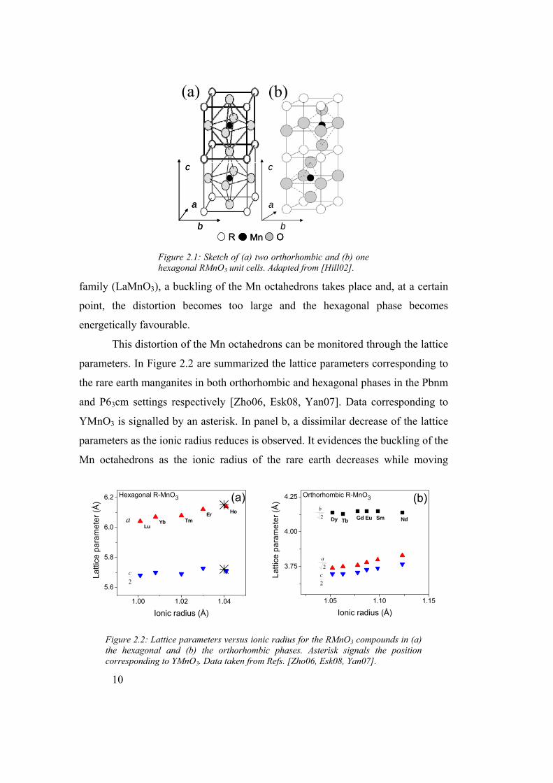
10
family (LaMnO3), a buckling of the Mn octahedrons takes place and, at a certain
point, the distortion becomes too large and the hexagonal phase becomes
energetically favourable.
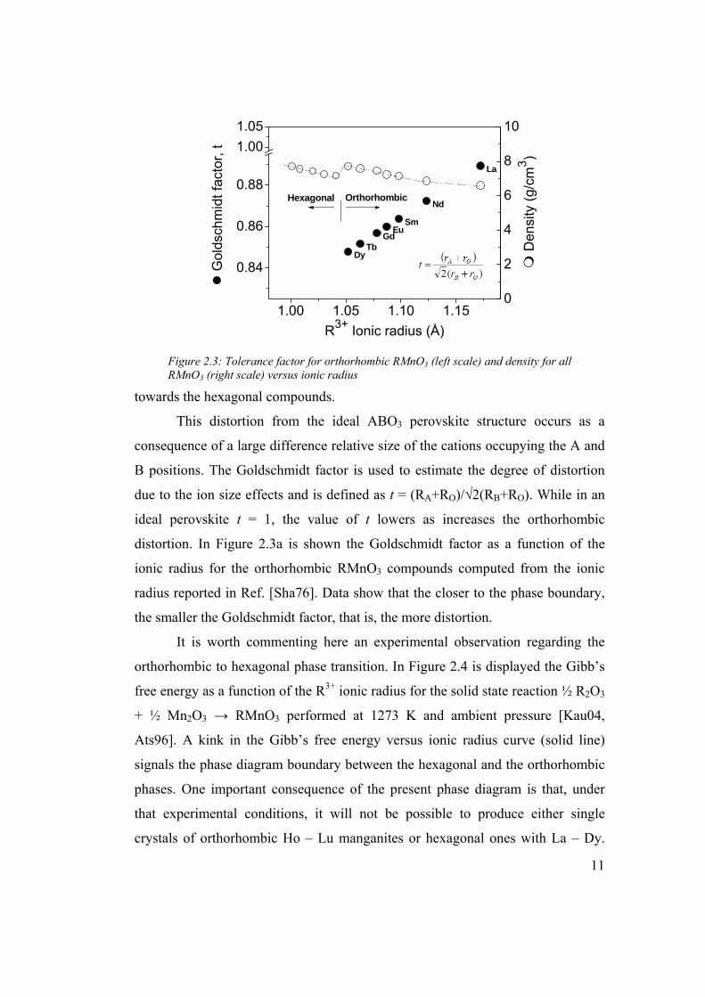
This distortion of the Mn octahedrons can be monitored through the lattice
parameters. In Figure 2.2 are summarized the lattice parameters corresponding to
the rare earth manganites in both orthorhombic and hexagonal phases in the Pbnm
and P63cm settings respectively [Zho06, Esk08, Yan07]. Data corresponding to
YMnO3 is signalled by an asterisk. In panel b, a dissimilar decrease of the lattice
parameters as the ionic radius reduces is observed. It evidences the buckling of the
Mn octahedrons as the ionic radius of the rare earth decreases while moving
b
a
c
b
a
c
b
a
c
MnR OMnR O
(a) (b)
Figure 2.1: Sketch of (a) two orthorhombic and (b) one hexagonal RMnO3 unit cells. Adapted from [Hill02].
1.00 1.02 1.04
5.6
5.8
6.0
6.2
HoErTmYb
Lu
2c
a
Latti
ce p
aram
eter
(Å)
Ionic radius (Å)
Hexagonal R-MnO3 (a)
1.05 1.10 1.15
3.75
4.00
4.25
NdSmEuGdTbDy
(b)
2c
2b
2a
Latti
ce p
aram
eter
(Å)
Ionic radius (Å)
Orthorhombic R-MnO3
Figure 2.2: Lattice parameters versus ionic radius for the RMnO3 compounds in (a) the hexagonal and (b) the orthorhombic phases. Asterisk signals the position corresponding to YMnO3. Data taken from Refs. [Zho06, Esk08, Yan07].
11
towards the hexagonal compounds.
This distortion from the ideal ABO3 perovskite structure occurs as a
consequence of a large difference relative size of the cations occupying the A and
B positions. The Goldschmidt factor is used to estimate the degree of distortion
due to the ion size effects and is defined as t = (RA+RO)/√2(RB+RO). While in an
ideal perovskite t = 1, the value of t lowers as increases the orthorhombic
distortion. In Figure 2.3a is shown the Goldschmidt factor as a function of the
ionic radius for the orthorhombic RMnO3 compounds computed from the ionic
radius reported in Ref. [Sha76]. Data show that the closer to the phase boundary,
the smaller the Goldschmidt factor, that is, the more distortion.
It is worth commenting here an experimental observation regarding the
orthorhombic to hexagonal phase transition. In Figure 2.4 is displayed the Gibb’s
free energy as a function of the R3+ ionic radius for the solid state reaction ½ R2O3
+ ½ Mn2O3 → RMnO3 performed at 1273 K and ambient pressure [Kau04,
Ats96]. A kink in the Gibb’s free energy versus ionic radius curve (solid line)
signals the phase diagram boundary between the hexagonal and the orthorhombic
phases. One important consequence of the present phase diagram is that, under
that experimental conditions, it will not be possible to produce either single
crystals of orthorhombic Ho – Lu manganites or hexagonal ones with La – Dy.
1.00 1.05 1.10 1.15
0.84
0.86
0.88
1.001.05
0
2
4
6
8
10
La
Nd
SmEu
GdTb
Dy
Hexagonal
Gol
dsch
mid
t fac
tor,
t
R3+ Ionic radius (Å)
Orthorhombic
Den
sity
(g/c
m3 )
Figure 2.3: Tolerance factor for orthorhombic RMnO3 (left scale) and density for all RMnO3 (right scale) versus ionic radius

12
Extrapolation of the data corresponding to both phases allows estimating the
energy difference among the stable and metastable phases. It is observed that such
energy gap has a minimum in at Ho and Y cations.
Detailed inspection of Figure 2.4 reveals that the average energy gap
between the formation of stable and metastable phases in bulk is of the order of
few kJ/mol. However, when the material is grown as a thin film on a substrate, the
interface energy must also be considered. Estimation of this energy contribution
[Gor02] in the case of coherent growth leads to a value smaller than the energy
gap mentioned in the formation of bulk phases. In this case, the previous
thermodynamic diagram still holds and the stable phase is determined by the ionic
radius of the rare earth. However, in the case of incoherent interfaces, the
additional energy cost can be up to 2 orders of magnitude larger [Gor02]. In this
scenario, the stable phase will be ruled by the film-substrate interface energy and
the role of the ionic radius will be secondary. Kaul and co-workers reported that
the epitaxial stabilization of metastable hexagonal [Gor02, Gra03] or
orthorhombic [Bos01, Gor02] rare earth manganites can be obtained by the proper
selection of the substrate.
Apart from the epitaxial stabilization, two other routes have been reported
in order to obtain metastable orthorhombic RMnO3 samples. On one hand, since
the density in the orthorhombic phase is larger than in the hexagonal phase
(Figure 2.3a) if a higher pressure is applied during the formation of the compound
Figure 2.4: (a) Free Gibb’s energy for the formation of the RMnO3 as a function of the ionic radius of the rare earth [Kau04].
13
the orthorhombic phase will be favoured. For instance, high pressure synthesis
allows producing bulk polycrystalline samples of Lu – Ho in the orthorhombic
phase [Wai67]. On the other hand, ‘soft’ chemistry procedures [Bri97] produced
polycrystalline samples of orthorhombic YMnO3 and HoMnO3. Note that none of
these procedures allowed producing orthorhombic single crystals of RMnO3 with
ionic radius larger than Ho, that is, when the stable phase in bulk is hexagonal. On
the other side, the production of hexagonal single crystals of metastable DyMnO3
has been reported [Iva06]. Since the extrapolation of the hexagonal regime is
located above the orthorhombic region in the free Gibb’s energy plot, it is
reasonable that if there was an additional energy contribution during the formation
of the compounds the hexagonal phase could be formed. Indeed, a phase transition
onto the hexagonal phase is observed for DyMnO3 at 1600 ºC and, by a proper
quench, the hexagonal phase is retained at room temperature [Iva06]. The same
argument cannot be applied to subsequent rare earths because the required
temperature would be larger than the melting point.
2.2 Introduction to orthorhombic RMnO3
2.2.1 Magnetic properties
Neutron diffraction experiments [Alo97, Oka08, Hua06, Ye07, Kim03b,
Muñ01, Muñ02, Kaj04, Jir85, Wu00] indicate that all orthorhombic RMnO3
compounds are antiferromagnetic below a Néel temperature (TN) ranging from 40
to 100 K depending on the ionic radius as shown in Figure 2.5a.
Although all neutron diffraction experiments for the RMnO3 compounds
ranging from Nd – Dy conclude that the spin ordering along the c direction is
antiferromagnetic, there have been observed three different magnetic orderings in
the ab plane as summarized in Figure 2.5a: ferromagnetic (that is, A-type
antiferromagnet), collinear sinusoidal modulation and spiral modulation. If the
orthorhombic metastable compounds (Ho – Lu) are also taken into account, one
more antiferromagnetic ordering (E-type) must be added in the diagram.
14
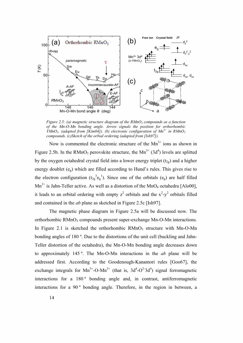
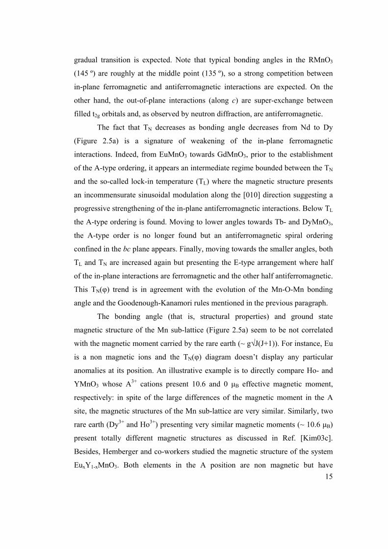
Now is commented the electronic structure of the Mn3+ ions as shown in
Figure 2.5b. In the RMnO3 perovskite structure, the Mn3+ (3d4) levels are splitted
by the oxygen octahedral crystal field into a lower energy triplet (t2g) and a higher
energy doublet (eg) which are filled according to Hund’s rules. This gives rise to
the electron configuration (t2g3eg
1). Since one of the orbitals (eg) are half filled
Mn3+ is Jahn-Teller active. As well as a distortion of the MnO6 octahedra [Alo00],
it leads to an orbital ordering with empty z2 orbitals and the x2-y2 orbitals filled
and contained in the ab plane as sketched in Figure 2.5c [Ish97].
The magnetic phase diagram in Figure 2.5a will be discussed now. The
orthorhombic RMnO3 compounds present super-exchange Mn-O-Mn interactions.
In Figure 2.1 is sketched the orthorhombic RMnO3 structure with Mn-O-Mn
bonding angles of 180 º. Due to the distortions of the unit cell (buckling and Jahn-
Teller distortion of the octahedra), the Mn-O-Mn bonding angle decreases down
to approximately 145 º. The Mn-O-Mn interactions in the ab plane will be
addressed first. According to the Goodenough-Kanamori rules [Goo67], the
exchange integrals for Mn3+-O-Mn3+ (that is, 3d4-O2-3d4) signal ferromagnetic
interactions for a 180 º bonding angle and, in contrast, antiferromagnetic
interactions for a 90 º bonding angle. Therefore, in the region in between, a
YY
(a)
a
b
c
(c)
(b)
Mn3+ 3d4
(o-YMnO3)
Free ion Crystal field JT
eg
t2g
dz2
dx2-y
2
dxy
dxz, dyz
Figure 2.5: (a) magnetic structure diagram of the RMnO3 compounds as a function of the Mn-O-Mn bonding angle. Arrow signals the position for orthorhombic YMnO3. (adapted from [Kim04]). (b) electronic configuration of Mn3+ in RMnO3 compounds. (c)Sketch of the orbial ordering (adapted from [Ish97]).
15
gradual transition is expected. Note that typical bonding angles in the RMnO3
(145 º) are roughly at the middle point (135 º), so a strong competition between
in-plane ferromagnetic and antiferromagnetic interactions are expected. On the
other hand, the out-of-plane interactions (along c) are super-exchange between
filled t2g orbitals and, as observed by neutron diffraction, are antiferromagnetic.
The fact that TN decreases as bonding angle decreases from Nd to Dy
(Figure 2.5a) is a signature of weakening of the in-plane ferromagnetic
interactions. Indeed, from EuMnO3 towards GdMnO3, prior to the establishment
of the A-type ordering, it appears an intermediate regime bounded between the TN
and the so-called lock-in temperature (TL) where the magnetic structure presents
an incommensurate sinusoidal modulation along the [010] direction suggesting a
progressive strengthening of the in-plane antiferromagnetic interactions. Below TL
the A-type ordering is found. Moving to lower angles towards Tb- and DyMnO3,
the A-type order is no longer found but an antiferromagnetic spiral ordering
confined in the bc plane appears. Finally, moving towards the smaller angles, both
TL and TN are increased again but presenting the E-type arrangement where half
of the in-plane interactions are ferromagnetic and the other half antiferromagnetic.
This TN(φ) trend is in agreement with the evolution of the Mn-O-Mn bonding
angle and the Goodenough-Kanamori rules mentioned in the previous paragraph.
The bonding angle (that is, structural properties) and ground state
magnetic structure of the Mn sub-lattice (Figure 2.5a) seem to be not correlated
with the magnetic moment carried by the rare earth (~ g√J(J+1)). For instance, Eu
is a non magnetic ions and the TN(φ) diagram doesn’t display any particular
anomalies at its position. An illustrative example is to directly compare Ho- and
YMnO3 whose A3+ cations present 10.6 and 0 μB effective magnetic moment,
respectively: in spite of the large differences of the magnetic moment in the A
site, the magnetic structures of the Mn sub-lattice are very similar. Similarly, two
rare earth (Dy3+ and Ho3+) presenting very similar magnetic moments (~ 10.6 μB)
present totally different magnetic structures as discussed in Ref. [Kim03c].
Besides, Hemberger and co-workers studied the magnetic structure of the system
EuxY1-xMnO3. Both elements in the A position are non magnetic but have

16
YMnO3 TbMnO3
Figure 2.6: sketch of the magnetic structure below the locking temperature for (a) YMnO3 and (b) TbMnO3 compounds. For clarity, the modulation period in (a) has been magnified. Adapted from [Ken05].
different ionic radius. The progressive Y- doping allows modifying the topology
(unit cell volume and bonding angle) in the same manner as by changing the rare
earth in the A position. Their work indicates that the same phase diagram and its
derived dielectric features are recovered, thus discarding a major role of the rare
earth on the Mn sub-lattice ground state [Hem07].
Within the magnetic phase diagram shown in Figure 2.5a, the lattice
parameters change less than 1.5% and the bonding angle 4º. Although such
changes are relatively large when considering bulk materials, are not unusual
variations of the lattice parameters when comparing the bulk materials with
epitaxially strained thin films. On these grounds, it is reasonable to expect that,
when growing epitaxial RMnO3 thin films, the substrate-induced strain will
change the films’ lattice parameters and, in consequence, the resulting magnetic
structure can be radically modified. Therefore, a fine control of lattice parameters
by controlling the experimental growth conditions is expected to allow tuning the
magnetic properties as it will be discussed in Chapter 4.
A closer look will be devoted to the magnetic structures of orthorhombic
YMnO3 and TbMnO3 because these materials have focussed a relevant part of the
work contained in Chapter 4. Both materials present a paramagnetic-
antiferromagnetic transition at TN ~ 40 K followed by a E-type collinear ordering
with a sinusoidally modulation along the b direction. The period of the

17
modulation depends on the temperature. At TL ~ 28 K, the period is 0.435
[Muñ02] and 0.28 [Kim03b] for YMnO3 and TbMnO3, respectively. Below this
temperature, TbMnO3 orders magnetically in a spiral structure contained in the bc
plane with a temperature-dependent period, incommensurate with the lattice
[Ken05]. On the other hand, YMnO3 magnetic structure remains incommensurate
but with the modulation period fixed kx = 0.435 [Muñ02]. Note that, when
comparing the antiferromagnetic structures, YMnO3 remains collinear and
TbMnO3 presents a non collinear arrangement. Representations for the collinear
(YMnO3-like) and non-collinear spiral (TbMnO3-like) orderings are sketched in
Figure 2.6.
2.2.2 Ferroelectricity and magnetoelectric coupling
The observation of net electrical polarization in the orthorhombic
compounds such us GdMnO3, TbMnO3 and DyMnO3 [Kim03, Kim05] was not a
priori expected because these structures are centrosymmetric. Anomalies in the
dielectric constant at the onset of the antiferromagnetic ordering in orthorhombic
YMnO3 and HoMnO3 were also reported [Lor04]. Later, ferroelectricity was
observed in these compounds [Lor07], also centrosymmetric. Intriguingly enough,
the ferroelectricity and/or the dielectric anomalies appeared in the magnetically
ordered states and could be modified by magnetic fields.
In the recent years, explanations for the ferroelectricity in orthorhombic
rare earth manganites have been developed (see for instance the reviews in Ref.
[Che07], [Kho09]). The explanations can be classified in two categories: the first
arises from the non-collinear spiral ordering and the second on the non-symmetric
interactions in E-type antiferromagnets. For both causes, atomic displacements
occur and, as a consequence, electrical dipoles are created. Since these
displacements arise from magnetic interactions in an ordered state, the induced
electric dipoles are ordered as well.
In non-collinear spiral-ordered antiferromagnets, the microscopic origin of
polarization is related to the atomic displacements of the oxygen atoms, lifted out

18
of the plane containing the Mn atoms, which remain at the same positions
[Kat05]. The displacements are caused by the Dzyaloshinskii-Moriya exchange
interactions between Mn moments which induce an on-phase shift of the bridging
ligands (oxygen atoms) thus creating a polar state. It is predicted that P ~ rij x (Si
x Sj) [Kat05], that is, the electrical polarization increases as the non-collinearity of
the magnetic moments also increases. The existence of such ferroelectricity was
also explained by symmetry arguments [Ken05], and from a phenomenological
approach [Mos06]. The predicted polarization in this case is of the order 0.1
μC/cm2 [Kat05].
In E-type antiferromagnets, as a result of the asymmetric magnetic
interactions between up-up and up-down spins, there is a shift of the oxygens and
Mn atoms within the ab plane. The overall displacement along the c and b
directions cancel each other, but it is not so along the [100] direction. Therefore
net electrical polarization along the [100] direction comes up [Ser06]. The
polarization is predicted to depend on the Mn-O-Mn bonding angle and, in this
case, is of the order μC/cm2 [Ser06].
According to these models, the canting and the bonding angle determine
the electrical polarization. It turns out that a modification of the magnetic
topology, for instance induced by magnetic fields, will lead to changes in the
dielectric properties. Starting from a phenomenological Ginzburg-Landau theory
it has been reported [Kim03b] that, at temperatures close to the magnetic
transition, the change in the dielectric permittivity should behave as ε ∼ α·M2,
where α is the magnetoelectric coupling coefficient. Illustrative examples of this
M2 dependence have been previously reported for ε-Fe2O3 nanoparticles [Gic07]
and the similar multiferroic compound BiMnO3 [Kim03b].
Finally, in connection with the motivation of this thesis, it must be recalled
here that in thin films, the lattice distortion (distances, and bonding angles) due to
the epitaxial strain is expected to introduce changes in the magnetic structure and
in the concomitant dielectric properties. This is the tool that this thesis aims to
exploit to modify the magnetoelectric properties of these materials.

19
2.3 Introduction to hexagonal RMnO3
2.3.1 Magnetic properties
Neutron diffraction [Muñ00, Muñ01b, Par02, Fab08, Tsa04] have revealed
that hexagonal rare earth manganites (R = Y – Lu) are antiferromagnetic and that
TN increases from 70 K to 90 K as the ionic radius decreases. Experiments
indicate that the magnetic moment of the Mn atoms confined into a two-
dimensional frustrated triangular lattice in the (0001) plane. Magnetometry
measurements in the paramagnetic region agree that the measured effective
magnetic moment matches the expected √(μMn2+μRE
2). There is a notable
dispersion in the reported extrapolated Curie Temperatures (θp) measured on
single crystals [Kat01, Sug02] and polycrystalline samples [Hua97, Muñ00,
Esk08]. Recently, it has been shown that the paramagnetic regime in hexagonal
RMnO3 (and as a consequence the θp) is highly anisotropic and is ruled by the rare
earth and not the average ferromagnetic or antiferromagnetic Mn interactions
[Sku09].
In contrast to the orthorhombic structure, in the hexagonal phase, the Mn is
in-plane coordinated to other three (and not four) Mn atoms and the bonding
Mn3+ 3d4
(h-YMnO3)
Free ion Crystal field
dz2
dxy, dx2-y2
dxz, dyz
(a) (b)
ϕ = 90º ϕ = 0ºϕ = 90º ϕ = 0ºϕ = 90º ϕ = 0º
Figure 2.7: (a) electronic structure of the Mn3+ ions in the hexagonal YMnO3. (b)Magnetic phase diagram for the hexagonal RMnO3 compounds (R = Y – Lu). In the bottom schemes the filled and empty symbols correspond to spins located at z = 0 and z = 1/2, respectively [Fie00].

20
angles are 120 º. The electronic structure is also different: according to Aken et
al., the eg orbitals x2-y2 and the 3z2-r2 are not degenerate as in the orthorhombic
perovskites, but x2-y2 is degenerate with xy [Ake01]. This electronic stucture is
sketched in Figure 2.7a. Therefore, the Mn3+ (3d4) ground state is non
degenerated and the z2 orbitals are empty in agreement with the shorter Mn-O
bonding distances along the c axis than in the ab plane [Ake00].
For the in-plane 120 º angles, antiferromagnetic coupling is expected for
in-plane Mn-O-Mn super-exchange interactions between 3d4 orbitals. The out-of-
plane interactions are no longer super-exchange as in the orthorhombic structure
and in the hexagonal phase they are super-super-exchange (Mn-O-O-Mn) as is
observed in Figure 2.1 (panels a and b). The inter-plane interactions are then
notably weaker [Goo63] in contrast to the strong in-plane interactions that confine
the spins in the ab plane. Within this scenario, two parameters remain unfixed:
first, the inter-plane interaction and, second, the in-plane rotation of the spins
respect to the crystal directions. These Second Harmonic Generation (SHG)
measurements, reported by the group of Fiebig, allowed discriminating among
these scenarios [Fie00]. In contrast, neutron diffraction experiments could not
univocally determine the magnetic structure because the predicted intensities in
the patterns are very similar in all cases [Muñ00, Par02]. Fiebig et al. concluded
that inter-plane interactions among spins in the same crystal direction are
ferromagnetic [Fie00]. The magnetic structures of the hexagonal RMnO3 are
summarized in Figure 2.7b. The filled and empty symbols of the bottom schemes
correspond to spins located in the z = 0 and z = ½ planes, respectively. The tilt
angle (φ) of the spins respect to the lattice remains as free parameter and there are
three possible scenarios: φ = 0 º, φ = 90 º and the intermediate values. In the case
of YMnO3, φ = 0 º in the entire antiferromagnetic regime; for Er – Yb corresponds
φ = 90 º. In the case of Ho- and LuMnO3, the antiferromagnetic ordering
corresponds to φ = 90 º at high temperatures, but it turns onto φ = 0 º as
temperature decreases. This phase diagram corresponds to the ground state
magnetic structures. If a magnetic field is applied, different structures are
observed as described in Ref. [Fie03, Yen07]. It is found that the phase diagrams

21
for compounds presenting non-magnetic cations in the A-site (such as LuMnO3 or
YMnO3) are not modified by magnetic fields thus indicating an active role for the
rare earth cation magnetism. It is worth mentioning here that the magnetic
structure for hexagonal compounds is still disputed. Recent neutron diffraction
experiments on hexagonal YMnO3 point to the intermediate case (0 º< ϕ < 90 º)
shown in Figure 2.7b as the magnetic structure [Bro06] or, as shown in Ref.
[Lee06], it cannot be completely ruled out the presence of significant inter-plane
antiferromagnetic interactions.
2.3.2 Ferroelectricity
RMnO3 compounds are ferroelectric with a TC in the 600-1000 K range,
well above the room temperature [Fuj96a]. The polar axis is along the [0001]
direction and the typical values for the spontaneous polarization and the coercitive
fields are around 5.5 μC/cm2 and 10 kV/cm, respectively [Fuj96a].
In the so-called “proper” ferroelectrics, electric dipoles are created by the
atomic displacements induced by electronic activity. However, the two most
common driving mechanisms are not favoured in YMnO3: firstly, the Mn3+ (3d4)
atom with partially filled d orbitals does not favour the charge transfer from the
oxygen 2p orbitals and, secondly, in the A-site there is Y3+ which does not present
lone pairs. In contrast, the origin of the “improper” ferroelectricity in hexagonal
RMnO3 is a structural phase transition as reported by Van Aken et al. [Ake04]
from their early measurements in laboratory X-ray diffration [Ake00] and later
confirmed by synchrotron X-ray [Kat02] and neutron diffraction studies [Kat02,
Jeo07]. At T > Tc, the hexagonal RMnO3 compounds belong to the P63/mmc
space group which is centrosymmetric and, as a result, no spontaneous electric
dipoles can be formed. Below Tc, the space group becomes P63cm which is no
longer centrosymmetric. The main difference between the two space groups is that
in the first one all ions are confined in parallel planes whereas, in the second case
only the Mn ones are constrained to the planes. This is caused by a geometric
effect of tilting the MnO5 bipyramids below Tc which keeps the Mn atoms at the
22
same positions but, in the other side, causes a buckling of the Y atoms. As a
result, the center of positive and negative charge is no longer coincident and
electric dipoles are formed. The obtained polarization is smaller but still
comparable to conventional ferroelectrics such as BaTiO3 and PbTiO3: around 5
times and 15 times smaller, respectively.
2.3.3 Magnetoelectric coupling
In contrast to the orthorhombic RMnO3 where the ferroelectricity emerged
from the magnetic order, in the hexagonal phase the sources for both ferroic
orders are independent. In these cases, the coupling between polarization and
magnetization, if any, is expected to be much smaller. However, in similarity to
the orthorhombic RMnO3, anomalies in the dielectric permittivity have been
reported for Y-, Ho-, Yb- and LuMnO3 at the onset of TN suggesting a
magnetoelectric coupling [Kat01, Hua03, Lor04b, Ade08]. In the case of
HoMnO3, an additional anomaly in the dielectric constant is observed [Lor04b]
coinciding with the antiferromagnetic ordering of the Ho3+ atomic moments seen
in neutron diffraction experiments [Muñ01b]. The dielectric peaks anomalies are
sensitive to the application of a magnetic field as shown for Y- and HoMnO3
[Hua03, Lor04b]. Magnetoelectric effects have also been proved for YMnO3
[Nug07].
Clearly, there is a totally different magnetoelectric coupling mechanism to
be exploited in the hexagonal RMnO3. By SHG experiments it was observed that,
below TN, the ferroelectric domains walls were always accompanied by
antiferromagnetic domain walls in YMnO3 [Fie02]. However, the vice versa
statement was not observed: antiferromagnetic domains walls can exist detached
from ferroelectric domain walls. Via the clamping of the antiferromagnetic to the
ferroelectric domain walls it is reasonable to expect that the amount
antiferromagnetic domains can be controlled by an electric field. The generation
of a single electrical domain state via electrical bias is expected to sweep the
isolated antiferromagnetic domains, thus reducing the amount of

23
antiferromagnetic domain walls. The importance of this result lays on the fact that
antiferromagnetic domain walls can carry net magnetic moment and this critically
controls the exchange bias interaction of the antiferromagnetic RMnO3 with
contiguous ferromagnetic layers (more details on the exchange bias are presented
in Section 2.5 and Chapter 5).
2.4 State-of-the-art in epitaxial YMnO3 thin films
2.4.1 Orthorhombic epitaxial YMnO3 thin films
Although the stable phase of YMnO3 is hexagonal, the surface energy
contributed by the substrate’s symmetry can be determinant for the stabilization of
other phases. Due to this, the growth of orthorhombic YMnO3 thin films is
possible on four-fold symmetry surfaces such as SrTiO3(001), etc. The first report
on orthorhombic epitaxial stabilization of YMnO3 as thin films by was published
in 1998 aiming to grow new manganites in thin film in the frame of the research
on colossal magnetoresistance [Sal98]. The authors stabilized the orthorhombic
phase on SrTiO3(001) and NdGaO3(110) substrates. The first broad study
covering the epitaxial stabilization of the series of metastable orthorhombic rare-
earth manganites appeared in 2001 [Bos01], connected to a series of manuscripts
[Gor02, Kau04] on the epitaxial stabilization of the orthorhombic phase. These
first reports were followed by a gap of around three years most probably because
the orthorhombic phase of the RMnO3 presented less appealing functional
properties in comparison with the hexagonal ones: the orthorhombic cell was
centrosymmetric and, thus, not expected to be ferroelectric in contrast to the
hexagonal compounds showing Tc well above the room temperature [Fuj96a] and,
moreover, with the ferroic domain walls clamped [Fie02]. In this period, the
orthorhombic phase was seldom mentioned, unless in the case that it was obtained
as spurious phase on SrTiO3(111) substrates when aiming to grow the hexagonal
phase [Dho04].
After the report showing anomalies in the electrical permittivity related to
the antiferromagnetic ordering in bulk YMnO3 [Lor04] the interest was renewed

24
towards reproducing the results in thin films. In the frame of this thesis work,
methods to tune the out-of-plane texture of the thin films [Mar08] have been
reported, reproduced the dielectric anomalies and shown for the first time that the
epitaxial thin films presented ferromagnetic behaviour [Mar07]. At the same time,
emerged the theoretical and experimental reports on the ferroelectricity in
orthorhombic RMnO3 and, in particular, on YMnO3 [Lor07]. At that moment,
orthorhombic RMnO3 films became virtually multiferroic as they could present
simultaneous ferromagnetism and ferroelectricity. This definitely boosted the
research on this topic and a flurry of reports has appeared on the ferromagnetism
and dielectric anomalies in epitaxial orthorhombic YMnO3 thin films [Mar07,
Rub08, Dau09, Hsi08, Kir09, Lin09, Mar09, Rub09]. Although theoretical
explanations for the ferroelectricity has been reported [Kat05, Ser06], the
microscopic origin of the ferromagnetism remains under discussion. At the
present moment, the two more significant correlations reported for the
ferromagnetism are, on one hand, with the domain wall density [Dau09] and, on
the other hand, with the epitaxial strain [Mar09, Mar09b]. The investigation of the
origin of the ferromagnetism constitutes the objective of Chapter 4 in this thesis.
Summary of the groups growing orthorhombic RMnO3 thin films
Date Laboratory Technique Rare earth Refs
1998 Caen PLD Y Sal98
2001 - 2004 Moscow-Grenoble MOCVD Nd – Lu Bos01, Gor02,
Kau04
2008 until
now Hsinchu PLD Y, Ho Hsi08, Lin09
2008 until
now Groningen PLD Yb, Tb
Rub08, Rub09,
Dau09
2006 until
now Bellaterra PLD Y, Tb
Mar07, Mar08,
Mar09

25
Orthorhombic RMnO3 thin films: state-of-the-art summary
(i) Crystal texture: epitaxial stabilization of the orthorhombic phase is
achieved on SrTiO3 (STO), LaAlO3 (LAO), and NdGaO3 (NGO)
substrates.
On STO(001), single RMnO3(001) texture is obtained by all groups except
by Moscow-Grenoble which found that the RMnO3(001) coexists with
RMnO3(110). The group of Hsinchu did observe exclusively the (001)
texture in the broad range of deposition parameters investigated. On
LAO(001) and NGO(001) the RMnO3(110) texture is obtained.
Using STO(110), the group of Hsinchu obtained epitaxial YMnO3 thin
films with the b-texture at low temperatures (~650 ºC) turning gradually
into a-texture orientation at high temperatures (~850 ºC). The group of
Bellaterra reported b-oriented films at high temperature (800 ºC).
Using LAO(110), the group of Hsinchu (Y, Ho) obtained the b-texture
reporting, in the case of YMnO3, better the crystalline quality at higher
temperatures (~880 ºC).
On STO(111), the group of Bellaterra (YMnO3) and Groningen (YbMnO3)
obtained the (101) texture.
(ii) Crystal domain structure:
On STO(001) the groups of Hsinchu, Moscow-Grenoble and Bellaterra
reported 2 in-plane domains with the epitaxial relationships
[100]RMnO3//[110]STO and [010]RMnO3//[110]STO for the Y, Dy, Ho,
Tm and Lu orthorhombic magnanites. For TbMnO3, the group of
Groningen reported 4 in-plane domains clamping the [110]RMnO3 to the
[100]STO.
On STO(111), 3 in-plane domains have been reported for YMnO3 by the

26
group of Bellaterra .
On STO(110), single domain films are obtained in YMnO3 and HoMnO3.
The group of Hsinchu. reported single domain films also on LAO(110).
(iii) Bottom electrodes: the group of Bellaterra reported the growth of
YMnO3(001) on SrRuO3(001)/STO(001) and SrRuO3(110)/STO(110),
while the Groningen’s group reported the growth of YbMnO3(101) on
SrRuO3(111)/STO(111) substrates. Nb-doped substrates are used by the
groups of Bellaterra and Hsinchu.
(iv) Dielectric anomalies have been reported in the laboratories in
Bellaterra (Y), Groningen (Yb), and Hsinchu (Ho). Dependence of the
permittivity with the magnetic field has been presented only in the later
case.
(v) Ferromagnetic behaviour: is reported by the groups of Bellaterra (Y),
Groningen (Yb, Tb) and Hsinchu (Y, Ho).
(vi) Crystal domain size The group of Moscow-Grenoble observed that,
under same deposition conditions, but changing the rare-earth, the domain
size observed by HRTEM that the more mismatch, smaller domains.
Groningen’s group has recently reported that the domain size is reduced as
films’ thickness is reduced in TbMnO3 films.
2.4.2 Hexagonal epitaxial YMnO3 thin films
The first results on the growth of epitaxial thin films of hexagonal YMnO3
were reported by Fujimura et al. in 1996 [Fuj96b], aiming the development of
new ferroelectric materials. From that moment to now, the amount of laboratories
investigating thin films of hexagonal RMnO3 manganites has increased
dramatically. In this introduction will be addressed only the results on thin films
of YMnO3, which is usually grown by pulsed laser deposition. Results on other

27
deposition techniques and RMnO3 compounds are exhaustively listed in [Gel09].
Fujimura et al. initially focussed on the structural and ferroelectric
properties of the films [Fuj96ab, Ito03ab, Shi08] and, more recently, their interest
turned into its multiferroic properties [Mae07, Fuj07]. Magnetoelectric coupling
has been also explored: the dependence of the dielectric permittivity with both the
electric and magnetic field is presented in Ref. [Fuj07]. On the other hand,
Blamire and co-workers have reported on the epitaxial stabilization on different
substrates [Dho04] and on the multiferroic character. The integration of YMnO3
in an spin valve is shown in Ref. [Dho05]. Finally, our group has reported on the
growth and microstructure [Mar07b], the multiferroic character [Mar06b] and, as
it will be shown in Chapter 6, the electric control of the magnetization via the
integration of YMnO3 with a contiguous soft ferromagnetic layer [Mar06c,
Mar07c]. In addition, other groups have reported on epitaxial YMnO3 thin films
with focus on the structural characterization [Bal06] or on the dielectric
characterization [Rok00, Zho04].
Hexagonal YMnO3 thin films grown by PLD: state-of-the-art overview
(i) Substrates used and crystal texture:
Platinized sapphire, Pt(111)/Al2O3(0001), is found to be the most common
choice [Ito03a, Fuj07, Moe07, Shin08, Mar07b]. Si(111) is also widely
used using different buffers: Pt/ZrO2/SrO2 [Ito03a], Y2O3(111) [Ito03b],
Pt/SiO2 [Dho05], Pt/TiO2/SiO2 [Zho04], and SiON [Rok00]. Platinized
strontium titanate has also been used by us in Ref. [Mar07b]. Other groups
used single crystal substrates of GaN(001) [Bal06], MgO(111) [Fuj03],
Al2O3(0001) and Y:ZrO2(111) [Dho04]. All groups succeed in obtaining c-
oriented YMnO3 which is required for the ferroelectric applications. From
the reported full width at half maximum of rocking curves, better
crystalinity has been obtained on Y:ZrO2(111) [Dho04] with reported
values of 0.06º. In contrast, on Pt(111)-buffered substrates the reported
values lay in the 0.6 º – 1.3 º range [Ito03a, Mar07b, Moe07]. On
GaN(001) and Al2O3(0001), 0.9 º [Bal06] and 2 º [Dho04] are reported,

28
respectively.
(ii) Epitaxy and microstructure: RHEED patterns have been presented to
demonstrate the in-plane order [Ito03ab, Shin08]. More usually, X-ray
diffraction φ-scans [Mar07b, Dho04, Bal06]. Microstructure analysis by
transmission electron microscopy is presented in Refs. [Mar07b] and
[Bal06].
(iii) Magnetic properties: the antiferromagnetic character of the films has
been revealed indirectly through exchange bias experiments [Mar06,
Dho05]. Direct observation of antiferromagnetism has only been
performed by neutron diffraction in YMnO3 films grown by chemical
vapour deposition [Gel08].
(iv) Ferroelectricity: ferroelectric loops have been reported by Fujimura
and co-workers in 100 to 300 nm thick films at room temperature
[Fuj96ab, Ito03ab, Shi08, Mae07, Fuj07]. Dho et al. [Dho05] reported that
square ferroelectric loops were obtained for 200 nm thick films but neither
were shown as a Figure nor mentioned the measurement temperature.
Hysteretic capacitance-Voltage curves indicating ferroelectric behaviour
were presented in Ref. [Rok00] for 400 nm thick films at room
temperature.
(v) Electrical resistivity: High leakage in the thin films remains a critical
issue in the namely insulating hexagonal YMnO3. In the next are
summarized the resistivity values correspond to room temperature, and
citing directly from the references or estimation from reported leakage
current measurements. On Pt-buffered substrates, a resistivity of 106 Ω·cm
and 107 Ω·cm has been reported by us [Mar07c] and by Kim et al.
[Kim07], respectively. The maximum reported values on Pt-buffered
substrates corresponds to Fujimura et al. and are of the order of 109 Ω·cm
[Fuj07]. Directly grown on Y2O3-buffered Si the resistivity of h-YMO is
29
two orders of magnitude larger [Ito03b]. As a reference, the mentioned
values are orders of magnitude lower than the commonly used insulator
SiO2 with ρ ~ 1015 Ω·cm.
(vi) Magnetoelectric effects: changes of the dielectric permittivity close
to TN in YMnO3 thin films have been reported [Fuj07].
(vii) Exploitation of exchange bias: Dho et al. [Dho05] reported spin
valves of Cu sandwiched between permalloy (Py) films on top of
hexagonal YMnO3. Results showed that the exchange bias pinned the
magnetization of the contiguous Py layer. Also, the magnetization
switching induced by electric field in Py/YMnO3 heterostructures
[Mar06c] has been reported by the group of Bellaterra.
2.5 Exchange bias
When materials with ferromagnetic (FM)-antiferromagnetic (AF)
interfaces are cooled down below the Néel temperature (TN-AF < Tc-FM) under an
applied magnetic field, features in the magnetization loop of the FM material such
as shift in the applied field axis and/or a coercitive field increase are observed.
These effects, referred as Exchange Bias (EB), are caused by the interaction at the
interface of FM spins with uncompensated spins in the AF which create a net
magnetic field (Heb).
EB is widely used and implemented in many commercial devices. For
instance, in the field of spintronics, EB is used to tune the coercitive fields of one
of the FM layers involved. Despite this frequent use and the large research activity
in the phenomena after its discovery 50 years ago ([Rad07] lists up to 5 reviews in
the last 10 years) the mechanisms behind the EB are not completely understood.
An intuitive picture of the phenomena is sketched in Figure 2.8a.
Departing from picture (1), at TN < T < Tc, the magnetization of the FM is
saturated and oriented along the direction of the magnetic field (H). The AF
remains in the paramagnetic state so its spins remain randomly oriented. Then,
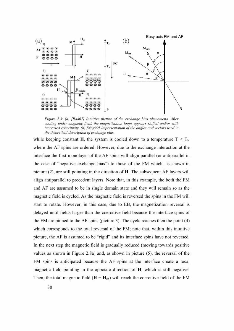
30
(a) (b)
Hc,left Hc,right
Easy axis FM and AF
Figure 2.8: (a) [Rad07] Intuitive picture of the exchange bias phenomena. After cooling under magnetic field, the magnetization loops appears shifted and/or with increased coercitivity. (b) [Nog99] Representation of the angles and vectors used in the theoretical description of exchange bias.
while keeping constant H, the system is cooled down to a temperature T < TN
where the AF spins are ordered. However, due to the exchange interaction at the
interface the first monolayer of the AF spins will align parallel (or antiparallel in
the case of “negative exchange bias”) to those of the FM which, as shown in
picture (2), are still pointing in the direction of H. The subsequent AF layers will
align antiparallel to precedent layers. Note that, in this example, the both the FM
and AF are assumed to be in single domain state and they will remain so as the
magnetic field is cycled. As the magnetic field is reversed the spins in the FM will
start to rotate. However, in this case, due to EB, the magnetization reversal is
delayed until fields larger than the coercitive field because the interface spins of
the FM are pinned to the AF spins (picture 3). The cycle reaches then the point (4)
which corresponds to the total reversal of the FM; note that, within this intuitive
picture, the AF is assumed to be “rigid” and its interface spins have not reversed.
In the next step the magnetic field is gradually reduced (moving towards positive
values as shown in Figure 2.8a) and, as shown in picture (5), the reversal of the
FM spins is anticipated because the AF spins at the interface create a local
magnetic field pointing in the opposite direction of H, which is still negative.
Then, the total magnetic field (H + Heb) will reach the coercitive field of the FM

31
at smaller (and even negative) values for the external magnetic field.
In the earliest model by Meiklejohn and Bean [Mei57], the energy per unit
area of an exchange bias system can be written as:
E = – H·MFM·tFM·cos(θ-β) + KFM·tFM·sin2(β) + KAF·tAF·sin2(α)
– Jeb·cos(β-α) Eq. 2.1
The symbols and vectors in the equation are sketched in Figure 2.8b. H is
the applied magnetic field, MFM the magnetization of the FM, tFM the thickness of
the FM, tAF the thickness of the AF, KFM and KAF are the anisotropy for the FM
and AF layers, and Jeb the interface coupling constant. Note that in this sketch the
easy axis of the FM and the AF are collinear. (θ-β) is the angle between the
magnetic field and the magnetization, β is the angle of the magnetization with the
FM easy axis, α is relative orientation of the antiferromagnetic arrangement
respect to its easy axis, and (β-α) is the angle between the orientation of the FM
and the AF spins. The first term accounts for the Zeeman energy, the second and
third terms for the magnetic anisotropy of the FM and the AF, and the final term
represents the EB interaction.
The second term can be neglected as the magnetic anisotropy of the FM is
generally smaller than in an AF. For simplicity, it will be assumed that the
magnetization loop is recorded along the easy axis of the FM, it is θ = 0. Then, the
minimization of the total energy with respect the angles β provides the conditions
and equations to obtain the coercitive fields Hc,right and Hc,left, in other words, at
which magnetic field occurs the reversal of magnetization. In EB systems, these
values are not expected to satisfy Hc,right = - Hc,left as in the FM materials.
Therefore, the total coercitivity Hc’ and the EB field (Heb) of the AF/FM system
can be calculated as:
2,, leftcrightc
eb
HHH
+= Eq. 2.2
32
2,,
'leftcrightc
c
HHH
−= Eq. 2.3
Depending on the value of R ≡ KAF·tAF / Jeb two scenarios are found. One
one hand, if R >> 1 then AF anisotropy is very large and the AF spins remain
rigid (as in the intuitive case presented). On the other hand, if R < 1, then the AF
spins are no longer rigid. In other words, the EB interaction is so strong and the
KAF so low that the pairs of AF spins simply follow the FM spins and no EB
effect is observed. The computed Heb and Hc’ for the case R >> 1 are:
FMFM
ebeb tM
JH
0μ−
= Eq. 2.4
FMFM
FMFMc tM
tKH
0'
··2μ
= Eq. 2.5
The complete calculation for intermediate R values is reported in Ref.
[Rad07]. The values predicted by the Meikeljohn-Bean model overestimate Heb
and underestimate Hc’. Additional models have been developed aiming to refine
the predictions as pointed out in several reviews (see for instance [Rad07]).
Spin compensation at the interface
The model assumed that the at the AF interface there are uncompensated
spins. In the case of fully compensated surfaces, such as in YMnO3(0001), the net
magnetic field induced by the AF on the top FM would be zero and, hence, zero
would be the EB interaction. In contrast, EB is being observed in many
compensated surfaces, even from single crystals of AF coated with FM materials
[Nog99]. Nogués et al. have catalogued the current models to describe such not
intuitive observations and, among other possible explanations, it turns out that the
existence of antiferromagnetic domain walls could be a source of exchange bias.
In particular, Goltsev et al. reported [Gol03] that YMnO3 antiferromagnetic

33
domain walls will extend along 102 – 104 unit cells due to its low in-plane
anisotropy. Of relevance in this thesis is that, as within the domain wall there is
net magnetic moment which can play the role of the uncompensated spins in the
EB phenomena. Another well known origin of net magnetic moment in
compensated surfaces is the disorder due to roughness which brings net magnetic
moment in the topmost surface of the films [Bla06, Kuc06].
Thickness of the AF and FM layers
As observed in Eq. 2.4, Heb follows a ~ 1/tFM dependence. Therefore for
the Py/YMnO3 system discussed in Chapter 6, it is convenient to keep the FM
layer as thin as possible to favour the EB effect. On the other hand, the FM layer
must be sufficiently thick to provide a large enough magnetic signal. Since Py
presents a Msat around 800 emu/cm3, thickness down to 5 nm will be sufficient to
obtain a signal in the SQUID of the order of 10-5 emu when coating an area of 8
mm2. On the other hand, the AF layer has to be enough thick in order to cause
R >> 1 and favour the EB effect. Therefore, the thickness of the AF layer should
larger than a critical thickness of tAF = Jeb/KAF. As a reference, Dho et al. observed
exchange bias in the Py/YMnO3 system with thickness of YMnO3 of 200 nm. It
suggests that a tAF of the order of hundreds of nanometers fulfills the R >> 1
condition.
Coercitive field
The coercitive field in the case R >> 1 remains the same as for a single FM
system (which tends to zero if the anisotropy KFM is very low). However, it is
generally observed an enhancement of the coercitive fields. Moreover, the trend
observed in the experiments indicates that the smaller KAF, the larger the Hc’
[Nog99]. This increase is intuitively simple to understand because in the case of
small KAF, the FM must drag all the AF spins, whereas in the case of larger KAF
the FM decouples from the AF as it cannot drag the contiguous AF spins. In the
case of YMnO3(0001) the in-plane anisotropy is very low due to its hexagonal
symmetry. Therefore the Py/YMnO3 sandwich is expected to present a remarkable
34
increase of coercitivity as Py is an extremely soft FM with Hc of the order of few
Oersteds.
Training effect
The training effect refers to the change of the hysteresis loop when
sweeping consecutively the applied magnetic field of a system which is in a
biased state. This effect seems to be related to partial reorientation of the AF
domains with each FM magnetization reversal as the AF spins try to find
energetically favourable configurations after each cycle [Nog99].
Training effect is not observed in all AF materials. Hoffmann reported a
list of AF materials that displayed or not the training effect. Interestingly, only the
uniaxial AF conserved the EB effect after cycling the magnetic field [Hof04]. In
this context, for hexagonal YMnO3, with a six-fold symmetry and very low in-
plane anisotropy, strong training should be expected in the standard magnetization
loop configuration. However, this limitation could be overcome, since training is
not observed in case of small reversible movements of the magnetization [Nog99].
In next section are described the anisotropic magnetoresistance measurements
were the magnetic field rotates the Py magnetization in a continuous way. As a
consequence, it could be more convenient than M(H) curves to investigate the
exchange bias in hexagonal YMnO3.
2.6 Anisotropic magnetoresistance with exchange bias
The magnetoresistance is the property of a material to change the value of
its electrical resistance when an external magnetic field is applied to it. For FM
materials this property depends on the angle (θa) formed by magnetization (M)
relative to the direction of the current (J) through the magnet and it is known as
anisotropic magnetoresistance (AMR). If magnetization (M) is saturated then it
follows the direction of the external magnetic field (Ha). Ha is rotated in the plane
of the sample from 0 º to 360 º while the electrical resistance R is recorded. The
resistivity as a function of the angle θa can be expressed as:

35
0 90 180 270 3600.0
0.5
1.0
θa (deg)
(ρ−ρ
0)/Δρ
FMJ
Ha
θa
FMJ
Ha
θa
R
(a) (b)
Figure 2.9: (a) AMR curve displaying the cos2(θa) dependence where θa is the angle of the magnetization of the material and the current J. (b) Sketch of the AMR experiment in a single FM material.
0 90 180 270 3600.0
0.5
1.0 h = 0.1 h = 0.25 h = 1.25 h = 5
θa (deg)
(ρ−ρ
0)/Δρ
θa
J
Heb
M
Ha
θeb
(a) (b)
Figure 2.10: (a) AMR curves corresponding to an AF/FM system as a function of h ≡ Ha / Heb. with θeb = 45 º (b) Sketch of the vectors in an AMR experiment with EB. The FM magnetization (M) follows the sum of the applied magnetic field (Ha) and the EB field (Heb)
( ) ( )aa θρρθρ 290º cos⋅Δ+= Eq. 2.6
where ρ90º is the resistivity measured at θa = 90 º and Δρ = ρ0º - ρ90º is the
difference between the parallel and perpendicular resistivity. An example of such
curve and a sketch of the measurement are shown in Figure 2.9, panels a and b,
respectively. Note that, as long as the FM layer is saturated, the resistivity
depends on the θa but not on |Ha|.
The presence of a contiguous AF layer to the FM will modify the total
magnetic field applied on the FM due to the exchange bias interaction. A new

36
magnetic field (Heb) must be taken into account and, as shown in Figure 2.10b,
the total field acting on the FM will be (Heb+Ha). Note that while Ha is rotating
during the AMR measurement, the Heb will remain rigid in a particular direction
(θeb) if the R >> 1 approximation is assumed. The θeb orientation is set by cooling
from T > TN down to T < TN under magnetic field. As a result, the shape of the
AMR curves are modified respect to Eq. 2.6 since the angle between J and M is
no longer θa because M is now not following Ha but the sum (Heb+Ha). The
analytical calculation for the AMR in the case of an EB system was derived by
Miller et al. [Mil96]:
( )( ) ( )
( )⎟⎟⎟⎟⎟⎟
⎠
⎞
⎜⎜⎜⎜⎜⎜
⎝
⎛
⎟⎟
⎠
⎞
⎜⎜
⎝
⎛−⋅⎟⎟
⎠
⎞⎜⎜⎝
⎛⋅+⎟⎟
⎠
⎞⎜⎜⎝
⎛+
⎟⎟⎠
⎞⎜⎜⎝
⎛⋅⎟⎟
⎠
⎞⎜⎜⎝
⎛+
⋅Δ+=
ebaeb
a
eb
a
aeb
aeb
a
HH
HH
HH
θθ
θθ
ρρθρ
cos21
coscos
2
2
90º
Eq. 2.7
Thus measuring the resistivity as a function of the angle θa allows
determining Heb ≡ |Heb|. Note that, in this case, the resistivity depends on both the
magnitude (Ha = |Ha|) and the relative direction to the current (θa) of the applied
magnetic field.
The most relevant parameter in equation 2.7 is h ≡ Ha / Heb which accounts
for the ratio of the applied magnetic field to the exchange bias field. In Figure
2.10a are shown some AMR curves corresponding to different h values. The most
remarkable feature is the transition from a two minima state in the h > 1 situation
to a only one minima in the case of h < 1. Two regimes can be identified
depending if the EB effects are dominant (h < 1) or not (h > 1). If the EB effects
are dominant, the total magnetization of the FM layer will be pinned by the AF
and the effects by the external rotating magnetic field (Ha) will be negligible. If M
remains rather constant, there is no change in the relative angle between M and J
and, therefore, the resistivity is expected to present smaller changes. In the other
limit, if h >> 1, the EB effects are negligible and the shape of the AMR curves for
single FM materials is recovered. Another interesting feature is the decrease of

37
amplitude of the AMR if h < 1, in contrast to the rather constant value for any
h > 1 curves. The smaller changes in resistivity when the EB effects are dominant
(h << 1) indicate that the changes in the angle between M and J are smaller, that
is, the magnetization of the FM is pinned by the AF. At the limit h → 0, resistivity
will depend only on the θeb direction which can be selected during the field cool.


39
3. Experimental techniques
This chapter is devoted to the description of the experimental techniques
used through the work in the present thesis. Firstly, the thin film growth
equipments are described. Afterwards, the characterization techniques used
throughout this thesis are presented. The ones where I have been directly involved
are presented first. Finally are described the characterization techniques used
occasionally as an external service or via collaborations.
3.1 Growth techniques
3.1.1 Pulsed laser deposition
YMnO3, YMn0.95Co0.05O3 and TbMnO3 thin films were deposited by
pulsed laser deposition at the Dept. Física Apliada i Òptica of the Universitat de
Barcelona. The support of Prof. Manuel Varela is acknowledged.
The set up is illustrated in Figure 3.1. A KrF excimer laser source emits
light pulses (τ = 34 ns, λ = 248 nm) that are focussed onto a stoichiometric target
of the desired composition at an angle of incidence of 45º. The frequency of the
pulses is set to 5 Hz. A mask which has variable size is located at the output
window of the laser to control the total outcoming energy. The beam is then
focussed on the target with fluences in the 1 – 3 J/cm2 range. The target is
mounted on a rotating platform to attain uniform erosion during the deposition as
the laser pulses hit the surface of the target. The combined action of the energy
absorption in a small volume, together with the short duration of each laser pulse,

40
Figure 3.1: Schematic illustration of the PLD system located at Dept. Física Aplicada at Universitat de Barcelona.
forces the ejection of the material away from the target. The formation of plasma
(called “plume”) follows, which expands very fast in the direction perpendicular
to the target plane. The plasma expansion is anisotropic and when reaches the
substrate at a distance of a few centimetres in the perpendicular direction, it is
confined laterally within a distance of the order of 1 cm.
The ejected material from the target is deposited onto a substrate, stick
onto a holder by silver paste and placed typically at a 5 cm away from the target.
The heater temperature is set in the 700 – 825 ºC range during the deposition. The
temperatures are measured by a thermocouple inserted in the heater block and
controlled by an automated PID system that controls the power supply. Substrate
temperature regulates the incoming particles mobility on the surface and its
growth mechanism but not critically the film thickness.
Previous to the start of the laser pulses sequence, a turbo-molecular and a
mechanical pump produce a vacuum in the 10-6 mbar range inside the deposition
chamber. Later, during the deposition an O2 atmosphere is created and controlled
via an automated mass flow and a manual butterfly valve. The pressure is set
typically in the 0.01 – 0.3 mbar range. The oxygen pressure reduces the speed
expansion of the plume and makes it broader. It causes the reduction of the
growth rate at high enough pressures. At the same time, the O2 pressure plays a
critical role in the growth of oxides, because part of the oxygen is incorporated in

41
Figure 3.2: Top view of the sputtering chamber at the ONERA-CNRS facilities (left) and detailed side view of the substrate holder (right)
the film helping to adjust the oxygen stoichiometry.
A short pre-ablation of about 200 pulses is performed using a shutter to
protect the substrates before the deposition in order to clean the topmost surface
of the target. The number of laser pulses is the most important parameter in order
to determine the thickness of the film. The usual growth rate is around 0.10 – 0.20
Ǻ/pulse.
Once the pulse sequence is finished the power supply is disconnected and
the vacuum valve is fully closed. Then, as the mass flow continues to introduce
oxygen in the chamber, the pressure increases gradually while the heater cools
down. Once the temperature of 530 ºC is reached, oxygen pressure in the chamber
is rapidly increased up to 1 atm and it is kept constant until the opening of the
chamber at temperatures below 50 ºC.
The RMnO3 targets used in the pulsed laser deposition were obtained by
mixing stoichiometric proportion of Mn2O3 and R2O3 oxides from commercial
powders of purity not lower than 99.9%. The precursors were preheated in a
furnace at 1000 ºC to remove eventual content of water. Then, they were weighed
and mixed mechanically up to homogeneity at room temperature and subsequently
sintered in a furnace at 1100 ºC for 12 hours at heating and cooling rates of 5 ºC
per minute. The resultant powder is transformed into pellets applying pressures up
to 5 tons for 15 minutes. Afterwards, pressure is released at 1 ton per minute rate
42
to prevent cracks on the pellets. The pellets are then reintroduced in the furnace
and the annealing procedure is repeated. Stoichiometry of the targets is confirmed
by electron dispersive x-ray spectroscopy. The correct phase is checked by XRD.
3.1.2 DC sputtering
Pt electrodes were grown by DC sputtering in a MPU-600S by Plassys
system in the ONERA-CNRS centre located at Toulouse during a 2 month long
stage in Toulouse in 2006.
The set up layout is depicted in Figure 3.2. The substrates are glued on a
sample holder using silver paste. Before introducing the holder into the sputtering
chamber, the holder is heated up to 100 ºC to dry the glue. Then, the holder is
introduced via a load lock inside the main chamber. There, it can be moved
vertically, horizontally and around the sample normal.
The sample holder is in contact with a heater which allows reaching
substrate’s temperature up to 800 ºC. The temperature is measured by a
thermocouple on the back of the plate on which the sample is fixed. The base
pressure of the system is up to 10-8 mbar reached by a cryogenic, a turbo-
molecular, and a mechanical pump. To generate the plasma an inert gas (usually
Ar) and a DC or RF electric field is used. Its partial pressure is controlled by flux-
meters attached to the chamber and controlled automatically. The atoms of the gas
are ionized and are accelerated by the electric field versus the target, which acts as
the cathode. The bombarded target emits atoms in a wide solid angle, which in a
first step travel towards a shutter. After a short pre-sputtering time, the shutter is
displaced and the target’s atoms now travel to the substrate. The typical growth
rate achieved is around nm/min range. The total thickness is controlled by the
duration of the deposition. Each sputter source is equipped with a shutter, which
allows controlling the deposition time within an accuracy of 1s. At the end of the
deposition time, the shutter on top of the plasma is closed and the sample moved
away. The RF source is switched off as well as the gas flows in order to reach
back the chamber base pressure. The sample is cooled down in vacuum and

43
afterwards removed from the chamber via the load lock.
3.1.3 Other depositions
The above mentioned depositions were carried out personally during the
thesis. However, some depositions have been carried out during the thesis by
collaborators and co-workers. These are listed below.
Recently, bottom Pt bottom electrodes have also been grown in ICMAB by
F. Rigato and M. Rajaram. Also, YMnO3 thin films have been recently deposited
by PLD by R. Bachelet at CIN2 in collaboration with J. Santiso. Some of these
films and bottom electrodes are present in the thesis work.
Top permalloy electrodes were deposited with the help of U. Lüders by
DC sputtering in CNRS-ONERA in the laboratory of J.-F. Bobo and later in
Universitat de Barcelona by M. Rubio and E. Bertran.
Top Pt electrodes for the dielectric characterization of the orthorhombic
RMnO3 films were deposited by I. Fina in the ICMAB facilities by RF sputtering.
3.2 Characterization techniques
3.2.1 X-ray diffraction
The X-ray diffraction experiments have been carried out at ICMAB using
a Siemens D500 as 2-circle diffractometer and Bruker D8 Advance area detector.
Some measurements have been performed at the Universitat de Barcelona in the
Serveis Científico-Tècnics using a 4-circle Philips-MRD diffractometer.
X-ray diffraction (XRD) is a non-destructive analysis which allows
studying the crystal structure of materials. It allows identifying phases, the
symmetry of the unit cell, its lattice parameters and the atomic positions. XRD is
based on the interpretation of the interference pattern created when an ideally
monochromatic beam of light is directed on a periodic structure. In crystalline
materials the periodic arrangement of atoms acts as this periodic structure. The x-
rays, whose wavelengths are of the order of an Å, are suitable for resolving the

44
Figure 3.3: Sketch of the angles involved in XRD experiments in (a) 2-circle and (b) in 4-circle goniometers
typical atomic planes spacing (periodicities) found in common oxides and metals
which are of the order of few Å.
In the particular case that concerns the present thesis, for thin films XRD is
used to investigate the thin film texture, whether the films are epitaxial, the
epitaxial relationship with the substrate, and changes in the lattice parameters
respect to the bulk values. It can also be used to detect parasitic impurity phases
and/or orientations in the film if their presence is significant enough to be
detected. Next are described the procedures to address all the questions mentioned
in the previous paragraph.
The texture of the films grown on a substrate is discussed first. A thin film
can grow either amorphous, polycrystalline and crystalline. In the first case no
periodic structure is formed at all. In the second case, the material is constituted
by crystalline grains oriented randomly in all directions. In the third case, the film
presents all the material ordered. In the latter case, the atomic planes parallel to
the surface of the films (also named the plane of the sample) constitutes the so-
called texture of the film. For an incident X-ray at an angle ω = θ l respect to the
plane of the sample (see Figure 3.3), the constructive interference condition for a
periodic arrangement of atomic planes parallel to the sample plane is given by the
Bragg’s law:

45
( ) λθ ·2sin·2 nd =ll Eq. 3.1
Where dl is the interplanar spacing, λ is the wavelenght of the used source
of X-rays and n is the order of diffraction.
The intensity recorded at the detector while scanning the θ angle with the
detector kept at 2θ angle respect to the incoming beam is known as a θ/2θ scan.
This procedure allows identifying the interplanar spacings present in the sample in
the direction perpendicular to the sample plane. In polycrystalline samples (for
instance, target powder) the grains are randomly oriented so all the interplanar
distances of one particular phase and compound can be observed in the spectra.
Since these distances are characteristic of each compound and phase, the θ/2θ
pattern allows identifying which phases and compounds are present. In the case of
epitaxial thin films, only a family of planes will be expected to be exactly oriented
perpendicular to the sample plane and thus observed in the θ/2θ scan. This family
of planes is the texture of the film. From the angular location of the peaks the
interplanar distance can be inferred so providing information on the epitaxial
strain along the out-of-plane direction. Appendix A. covers a correction of the
angular scale due to the virtually unavoidable sample misalignment.
The first figure of merit of the crystal quality of the film is monitored via
the rocking curves. These are based on relatively small range scan of the ω motor
around the nominal position of a diffraction peak keeping the detector fixed. A
Voigt-type profile of intensity is obtained which its full width at half maximum
accounts for the mosaicity in the out-of-plane direction of the sample.
The reflections not contained in the plane of the sample (so-called
“asymmetrical reflections”) can be explored by rotating the sample using the
following angles as shown in Figure 3.3:
φ, around the normal of the samples
Ψ, around in-plane axis of the film not contained in the diffraction plane
Now are described the analyses performed in asymmetrical configuration:
1. Phi-scans: in order to explore the in-plane texture of the film, the

46
sample is rotated around the azimuthal angle (φ) while the Bragg condition
for a certain asymmetrical reflection is satisfied. To allow that the
asymmetrical family of planes become parallel to the diffraction plane, the
sample is tilted in the Ψ angle while keeping the ω = θ condition. Then the
ϕ angle is rotated from 0 to 360 º bringing to Bragg condition as many
times as the in-plane symmetry of the film. This procedure allows
determining the relative in-plane orientation (epitaxial relationship)
between the film and the substrate. However, in ϕ-scans, accurate
optimization of the angular positions is required. Note that a small tilting
of the sample in the sample holder would produce a precession as the ϕ
angle is rotated. Then, intensity may be lost or even narrow peaks not
observed. The full width at half maximum of the observed peaks is used as
a signature of the in-plane texture quality.
2. Pole figures: It is a 2-dimensional map φ-Ψ which is an extension of the
phi-scans: several ϕ-scans performed at different Ψ. Since more recent
area detectors allow scanning the φ and the Ψ angles simultaneously, the
acquisition time is notably reduced. As an additional advantage, in area
detectors is not required to accurately optimize the angular positions prior
to the φ rotation as in the traditional φ-scans. The output allows
determining the epitaxial relationship in thin films in a single rotation of
the ϕ angle.
3. Reciprocal space maps: this procedure allows determining the lattice
parameters of the film if the epitaxial relationship is already known. This
scan corresponds to a series of standard θ/2θ scans performed in an θ ≠ ω
configuration. First, one (hkl) reflection which is not parallel to the texture
of the film must be selected. For simplicity, the discussion follows
assuming that a (h0l) reflection is chosen. The Ψ angle remains at zero
degrees and the φ angle must be moved as to locate the vector
perpendicular to the (h0l) plane investigated in the diffraction plane. Then

47
several θ/2θ scans are performed with the 2θ motor coupled to ω motor,
but instead of satisfying the ω = θ condition (like in θ/2θ symmetric scans)
now, ω = 2θ/2 – Ψ, where Ψ is the angle between [h0l] direction and the
texture of the film. The result is a 2-D map (2θ, ω) which display intensity
peaks. Then, for a certain (h0l) reflection the lattice parameters are found
as:
( ) ( )ωθθλ
−== sinsin;2x
x
qqha Eq. 3.2
( ) ( )ωθθλ
−== cossin;2z
z
qqlc Eq. 3.3
Although the final information are the lattice parameters, data are often
represented as a two dimensional map in the reciprocal space (qx and qy)
coordinates. The eventual error in the angular position would lead to
incorrect values for the lattice parameters; as a consequence, the scan
should be extended a few degrees in θ and ω as to contain also one
reflection from the substrate which will be used as reference. It is also
useful to collect a reflection from the substrate because the thin film may
have modified its lattice parameters due to epitaxial strain. Then the
maximum is not likely to be at the bulk positions. In this case, it is relevant
to determine whether the film has grown coherent with the substrate (if
both in-plane parameters from the film and the substrate present the same
in-plane parameters) or relaxed (otherwise).
Note that not all reflections of the film and the substrate are available to
perform reciprocal space maps. Firstly, the higher reflections which
involve small distances could not be resolved by standard X-ray machines.
On the other side, the reflections which too low Miller indices are not
allowed unless ω = 180º - θ – Ψhkl > 0 where Ψhkl corresponds to the angle
between the out-of-plane texture of the film and the [hkl] direction.

48
Point detector
Area detector
(a)
(b)
2θ
Ψ* *
Figure 3.4: (a) Sketch of the diffraction of the incoming X-rays in a perfect crystal indicating the advantages of using 2-dimensional detectors (collecting several reflections simultaneously) than point detectors. (b) Example of the frame obtained at the 2-dimensional detector showing reflections from single crystal substrate (asterisks) with a polycrystalline film on top (arrow).
Finally, is discussed the use of a 2-dimensional detector to identify traces
of polycrystalline material. In the XRD characterization of perfect epitaxial thin
films, when the X-ray beam is directed to the sample, the diffracted intensity of a
certain reflection is located exactly at a certain angular positions of the
goniometer as sketched in Figure 3.4a. In point-detector based equipments, the
detector must be placed a certain time at each location to collect, for each single
reflection, the diffracted intensity. In contrast, in the case of area detectors, many
reflections can be detected simultaneously with an evident saving of acquisition
time. The software allows converting into the usual 2θ and Ψ angles the position
of the reflections on the detector’s surface. Therefore, the single crystal reflections
appear at the 2θ coordinates according to the Bragg’s law and at the Ψ coordinates
according to the angle between the [hkl] direction and the out-of-plane direction.
Of relevance here is that, if polycrystalline material is present in the sample,
intensity for each (hkl) reflection will be placed at certain 2θ coordinates, but
spread all along the Ψ angles. As an example, it is shown in Figure 3.4b, the
detector’s intensity map for a polycrystalline thin film on a single crystal
substrate. High-intensity well-localized spots from the substrate are observed
(signalled by asterisks). In contrast, diffracted intensity from the thin films
appears to be spread along all the Ψ range (one of them signalled by an arrow).
49
Note that the conventional point detectors would need to scan several times
(devoting in each N scan t minutes and, in total, N·t minutes) whereas the 2-
dimensional detector is collecting the intensity for all Ψ and 2θ angles
simultaneously in a single scan in which it can be devoted a longer acquisition
time than in the individual scans using point-detectors. Therefore, it turns out that
the use of a 2-dimensional detector is a fast and effective technique to determine
the presence of polycrystalline material in thin films.
Further, the wide angle range of a single scan with a 2-dimensional
detector can be used to search for eventual impurities oriented in an unknown
direction in thin films. About 5 scans placing the 2-dimensional detector at 5
different locations are sufficient to cover the 2θ (5-100º) and Ψ (0- 90º) range in
reasonable time using standard X-ray tubes. If impurities were present, traces of
unexpected intensity should be observed within these scans. If all the reflections
observed corresponded to the expected positions for the film’s reflection it can be
concluded, within the experimental resolution, that significant impurities were not
present in the film.
3.2.2 X-ray reflectivity
XRR experiments have been carried out at ICMAB using a Rigaku
Rotaflex RU-200B.
X-ray reflectivity (XRR) is used to determine the film’s thickness in
monolayers or multilayers if the thicknesses are in the 10-100 nm range and the
roughness of top-most surface and interfaces is not too large.
In an XRR experiment an incoming X-ray beam reaches the film surface at
very low incident angle θi as shown in Figure 3.5a. The detector is placed always
at the right side, at an angle θo = θi. If the incident angle surpass the critical angle
of the film’s material, part of the incident beam is reflected (o1) and some part is
diffracted inside and out again (o2). Both beams are parallel and may present
interference fringes depending on the optical path travelled by o2 inside the film.
In contrast to X-ray diffraction experiments, it is now critical to take into account

50
0.5 1.0 1.5 2.0 2.5 3.0102
103
104
105
106
Inte
nsity
(arb
. uni
ts)
2θ (deg)
EXP
+13
+817
θc = 0.57º
SubstrateFilm
io1 o2
(a) (b)
θι θο
Figure 3.5: (a) Sketch of the XRR experiment with the incident rays “i”, the directly reflected light “o1”, the rays that refract inside the film and goes out again “o2”. Note that o1 and o2 are parallel. (b) Recorded data in an XRR experiment. Inset shows the derivative of the main panel as a procedure to determine the critical angle.
the refractive effects which are relevant at low angles (XRR) but can be neglected
at higher angles. The extra path can be derived using trigonometry and Snell’s
law. The final interference condition is given by:
λθθ ⋅=−⋅ nd c )(sin)(sin2 22 Eq. 3.4
Where d accounts for the thickness of the film, θ for the incident and
outgoing angle, θc for the critical angle, λ for the wavelenght of the X-rays source,
and n for the index of refraction. The previous equation corresponds to the
Bragg’s law with the corrections for refraction effects. The critical angle θc can be
obtained as the onset of the drop of reflectivity as shown in the inset in Figure
3.5b. It can also be calculated as θc = acos(n), being n the index of refraction
tabulated in several free databases available in the internet (see for instance
http://henke.lbl.gov/optical_constants). The critical angle is proportional to the
square root of the electronic density of the material.
To perform the analysis, θi is scanned (note that θo = θi moves accordingly)
in the range of 0.5 – 5º. Data presents the decay of reflectivity as expected by
Fresnel equations with the overlapped oscillations due to the interference between
o1 and o2.

51
The position of the maxima must be fitted versus the order of the
oscillation n. The slope contains d which is the thickness of the film. It is more
convenient to deal with the Eq 3.4 powered to 2:
222
22
)(sin2)(sin2 nddc =⎟
⎠⎞
⎜⎝⎛ ⋅
−⎟⎠⎞
⎜⎝⎛ ⋅ θ
λθ
λEq. 3.5
In this case the linear fitting allows determining the thickness and, from
the independent term, the critical angle which, as a crosscheck, must be consistent
with the obtained value by inspection of the derivative of the data (inset Figure
3.5b) and of the same order of the predicted and/or tabulated one. By this, the
eventual error in the assignation of n (the order of the oscillation) is prevented.
At the appendix is given the procedure to obtain the film’s thickness using
Fast Fourier Transform.
Finally, to determine the thickness of multilayers direct analytical
calculation is not possible. L.G. Parrat developed the calculation which allows
obtaining the reflectivity curve for a n-multilayer structure using as inputs the
thickness and index of refraction of each n-layer [Par54]. Then are compared the
calculation output with the experimental data while refining the inputs in each
iteration round. The final result is a best-fit set of parameters (thickness and
indexes of refraction) of the multilayer structure. For simplicity, in the present
thesis, the thicknesses in the case of the bilayers (hexagonal-YMnO3/Pt) have
been calculated from separated calibration of the growth rates.
3.2.3 SQUID magnetometry
Measurements of magnetization were performed at the ICMAB on a
SQUID system of Quantum Design. A maximum field of 7 T could be applied
and the accessible temperatures ranged within 5 K and 300 K. The measurement
is carried out by displacing at low frequency the sample along the vertical axis
around which two coils measure the flux variations. The induced voltage is
transmitted as electrical signal to a SQUID detector to determine the

52
Figure 3.6: pictures of the modified probe designed by V. Laukhin for the SQUID measurements with electrical biasing.
magnetization up to a resolution of order 10−7 emu. It is therefore suitable to study
thin films which signal is at least one order of magnitude higher. However,
several precautions have to be taken into account to remove the substrate
contribution and eventual ferromagnetic impurities. The procedures are described
in detail in Appendix C.
In order to perform the electric-field dependent measurements the probe of
the SQUID was modified by Prof. V. Laukhin in ICMAB (Figure 3.6). Two
braided wires depart from the sample located at the standard position in the straw.
The wires reach the top of the probe and then are connected to stretchable wires
which allow the oscillating displacements of the probe during the SQUID
measurement. At the tip of the SQUID probe there are the connections to plug
into a separated power source and electrically bias the YMnO3 sandwich during
the magnetic measurements. All connections preserve the vacuum inside the
SQUID.
3.2.4 Anisotropic magnetoresistance
The anisotropic magnetoresistance (AMR) measurements were performed
at the ICMAB by means of a PPMS (Physical Properties Measurements System,
Quantum Design). This equipment reaches temperatures down to 1.8 K. A
superconductive coil allows applying magnetic fields up to 9 T. The resistance is
measured by injecting current within a range of 5 nA - 5 mA, and the

53
SubstratePt electrodeYMnO3 filmPy electrode
(a) (b)
(c)
Figure 3.7: (a) Sketch of the multilayer structure in the AMR measurement. Contacts and direction of the magnetic field and current are displayed. (b) Picture of the sample mounted in the sample holder prepared. (c) Design view of photo in (b).
experimental resolution is about 10−8 V.
Four in-line graphite contacts (~ 1.75 x 0.2 mm2) were placed in the
sample surface as shown in Figure 3.7a to measure the magnetoresistance of the
top-most Py layer. Two contacts were used to inject current as the drop of
potential was measured by the other ones. RPy=VPy/IPy denotes the resistance
measured between two VPy contacts, where VPy is the measured voltage and IPy
the injected current fixed to 100 μA. Additional electrical contacts were made
using graphite paste on Py and bottom Pt electrode for electrical biasing (Ve) the
YMnO3 sandwich. AMR was measured by rotating the magnetic field in the film
plane while recording the film resistance R as a function of the angle θ between
the measuring current and the applied magnetic field (Ha). A Picture of the sample
and the contacts is shown in Figure 3.7b and sketched in Figure 3.7c.
3.2.5 Atomic force microscopy
The topographic Atomic Force Microscope (AFM) images in the present
work were obtained by a PicoSPM® equipment by Molecular Imaging at the
ICMAB. The scans were performed in dynamic tapping mode. The treatment of
the data was done by MountainsMap SPM-Imaging software (release 4.1.1).
In dynamic tapping AFM scans, a tip located at the edge of a cantilever is
54
oscillated in the direction perpendicular to the surface at frequencies in the 50 –
500 kHz range which are at or near the resonance of the assembly. The amplitude
of the oscillations is of the order of nanometres and is placed at 10 – 100 Å from
the surface. When the tip and the sample are separated de Van der Waals forces
cause them to weakly attract upon being too close and even tapping (contacting)
the surface where the electron clouds repulse each other. The assembly is capable
of precise XY (in the plane) displacements within a resolution of nanometres. Due
to the surface topography there are changes in the amplitude and phase of the
oscillations. These changes are monitored via a laser shining onto and reflecting
off the back of the cantilever and onto a segmented photodiode. From the changes
in the amplitude in each XY location in the surface, the topography of the surface
can imaged with sub-Å resolution in the vertical scale.
3.2.6 Dielectric measurements
Capacitance measurements were carried out using a LF4182 impedance
analyser (Agilent Co.) at ICMAB in the frame of the thesis of I. Fina. An
oscillating electric field of amplitude 100 mV and frequency of 100 kHz is
applied on the sample between top Pt electrodes (0.25 mm2, 200 nm thick) and the
bottom conductive substrates. In this geometry the electric field is applied
perpendicular to the sample surface. The analysis of the impedance of the sample
and its modelling via an RC parallel circuit allows determining the capacity and
the leaking current. Subsequently, assuming a parallel capacitor geometry
permittivity and the tangent losses are extracted. No significant dependence of the
derived parameters on frequency (between 100 Hz and 1 MHz) or in the excitation
voltages (between 5mV and 1 V) was observed.
In order to explore the temperature and magnetic field dependence of the
dielectric properties, the sample was inserted the sample inside a PPMS (the same
as in the AMR experiments) by Quantum Design. A commercial inset for
dielectric measurements was used in order to minimize the effect of electrical
noise.

55
3.2.7 Other characterization techniques
Transmission electron microscopy
Transmission electron microscopy (TEM) images were acquired at the
Serveis Científico-Tècnics located at the Universitat de Barcelona by a Jeol J2010
field emission gun microscope by S. Estradé, Dr. J. Arbiol and Dr. F. Peiro.
Electron Microscopes work exactly as their optical counterparts except
that they use a focused beam of electrons instead of light to ’image’ the specimen
and gain information as to its structure and composition. A stream of electrons is
formed by an electron source and accelerated toward the specimen using a
electrical potential. This stream is confined and focused using metal apertures and
magnetic lenses into a thin, focused, monochromatic beam, which is focused onto
the sample using a magnetic lens. Interactions occurring inside the irradiated
sample are affecting the transmitted electrons. The transmitted electrons are
detected and transformed into an image. With TEM, information on
microstructure is gained, but in the case of a high resolution TEM, also on
crystallographic properties like lattice parameter or on atomic-scale defects.
The sample was prepared in the cross-section geometry. First cut and then
polished into a thin foil specimen by mechanical polishing down to about 30 μm,
and then ion beam milling at 5 keV and 7º down to electrotransparency.
X-ray photoemission spectroscopy
X-ray photoemission spectroscopy (XPS) experiments were carried out
during three months stage in the group of Dr. R. Bertacco at Politecnico di Milano
(Como) in 2007 and, subsequently, at the Serveis Científico-Tècnics of
Universitat de Barcelona.
Photoemission spectroscopy is based on the photoelectric effect: when a
solid is irradiated by monochromatic photons, the photons excite the electrons
towards high energy levels or, if the energy is sufficient, release them from the
atom and then can be detected by an electron energy analyzer. The detected
electrons have a kinetic energy Ek = hω – Ei – φ , where hω is the energy of the

56
incoming photons, Ei is the binding energy and φ the work function of the electron
to escape the solid. The Ei energies vary from atom to atom and the detected
photoelectrons allow identifying the species present in the sample. The measured
distribution of the sharp peaks is superimposed on the secondary background,
which arises from electrons that have lost quasi-continuous amounts of energy
due to multiple inelastic scattering events in the crystal. However, the mean free
path of the electrons in the solid is of the order of 1-100 Å and, therefore, XPS
remains as a surface-sensitive technique. Within this range, the penetration depth
can be tuned by selecting the incident angle of the incoming photons.
At the laboratory of Como, the X-Ray Photoemission Spectroscopy (XPS)
experiments were performed in a PHI 5500 Multitechnique System (Physical
Electronics) with a monochromatic X-ray source (Al-Kα line, 1486.6 eV, 350 W),
calibrated using the 3d5/2 line of Ag with a full width at half maximum of 0.8 eV.
Spectra have been taken at room temperature and at 45º degrees of collection
angle. At the laboratory in Universitat de Barcelona (Serveis Científico-Tècnics),
the measurements were performed with an ESCA-PHI 5500. The system has a
monochromatic X-ray source (Al-Kα line). The spectra were taken at 45 º
collection angle.
57
4. Orthorhombic YMnO3: Ferromagnetism induced by epitaxial strain
In this chapter I describe the preparation, structural and functional
characterizations of the orthorhombic YMnO3 (o-YMO) thin films grown on
(001)-oriented SrTiO3 (STO) substrates. Structural studies by X-ray diffraction
indicate that the films are epitaxial, c textured and present two in-plane crystal
domains. It is shown that o-YMO unit cell parameters can be tuned by four
strategies: changing the oxygen pressure, the sample thickness, partial cationic
substitution and control of the oxygen vacancies via annealing. As a result, a
continuous spread of unit cell volumes can be obtained ranging from fully relaxed
(bulk-like) films up to a 3% reduction.
Pure antiferromagnetic behaviour is observed in the bulk-like films,
whereas an increasing weak ferromagnetic behaviour is superimposed as the unit
cell distortion increases. Analysis of the magnetic anisotropy reveals that it is
compatible with canting of the spins of about 1 º away from the b axis. Our results
are discussed in the frame of the very recent publications by other groups [Rub08,
Dau09, Hsi08, Kir09, Lin09, Rub09].
The chapter first presents the control of the epitaxial strain via O2 pressure
and sample thickness. Next, are presented the magnetic characterizations
indicating a strong correlation of the ferromagnetism with the epitaxial strain. The
growth and magnetic characterization of thin films with a 5 % substitution of Co
by Mn (YMCO) is presented subsequently. It is shown that, as Co presents a
smaller ionic radius, the epitaxial strain is different than in the undoped case;

58
however, the magnetic response is also correlated with epitaxial strain.
Next, epitaxial TbMnO3 (TMO) thin films are presented aiming to disclose
whether the ferromagnetism dependence on the unit cell distortion is also
applicable in a compound with a different cation in the A-site and a different
magnetic ground structure. The observed trends correlating strain and
ferromagnetism are exactly the same.
Finally, the dielectric properties are investigated. Models for
ferroelectricity emerging from magnetic order show dependencies of the
polarization on both canting and bonding angles. Interestingly, epitaxial strain
modifies both angles. It is shown that dielectric permittivity depends on the
magnetic field and magnetoelectric coupling can be tuned by the epitaxial strain.
Appendix D contains a description of how the amount of crystal domains
and the out-of-plane orientations can be controlled by the selection of the
substrate orientation. Single domain films with controlled texture are presented.
4.1 Structural study on epitaxial YMnO3/SrTiO3(001) thin films
4.1.1 Growth conditions
Samples have been grown by pulsed laser deposition (PLD) following the
procedure described in Chapter 3. As-received STO(001) substrates were used.
Miscut angle is nominally below 0.2 º. Table 4.1 summarizes the experimental
conditions for the samples discussed in this section. Substrate temperature was
785 ºC. Some samples were grown on 0.5% Nb-doped STO(001) substrates in
order to use them as bottom electrode in the dielectric measurements. Thickness is
obtained by X-ray reflectivity.
Name O2 pressure
(mbar)
Number of
laser pulses
Pulse energy
(mJ)
Fluence
(J/cm2)
Thickness
(nm)
210 0.1 4000 50 1.67 35
214 0.2 4000 50 1.67 31
213 0.3 500 50 1.67 5

59
Figure 4.1: (a) Marked growth rate (Å/pulse) dependence on the laser pulse energy in contrast to a rather constant behaviour as O2 pressure is changed. (b) Raw X-ray reflectivity curves for a selection of samples.
Name O2 pressure
(mbar)
Number of
laser pulses
Pulse energy
(mJ)
Fluence
(J/cm2)
Thickness
(nm)
211 0.3 4000 50 1.67 30
216 0.3 10000 50 1.67 76
212 0.4 6000 50 1.67 48.5
141 0.1 10000 90 2.25 119
140 0.2 10000 90 2.25 122
145 0.3 10000 90 2.25 111
253 0.3 1000 100 1.82 13.5
252 0.3 2000 100 1.82 27
257 0.3 3000 100 1.82 40
251 0.3 5000 100 1.82 67
248 0.1 10000 100 1.82 ~ 140
250 0.3 10000 100 1.82 ~ 137 Table 4.1: Sample list and its deposition conditions of the o-YMO films.
Samples are grouped in three different batches classified according to the
energy for the laser pulses. The film growth rate (Figure 4.1a) presents a marked
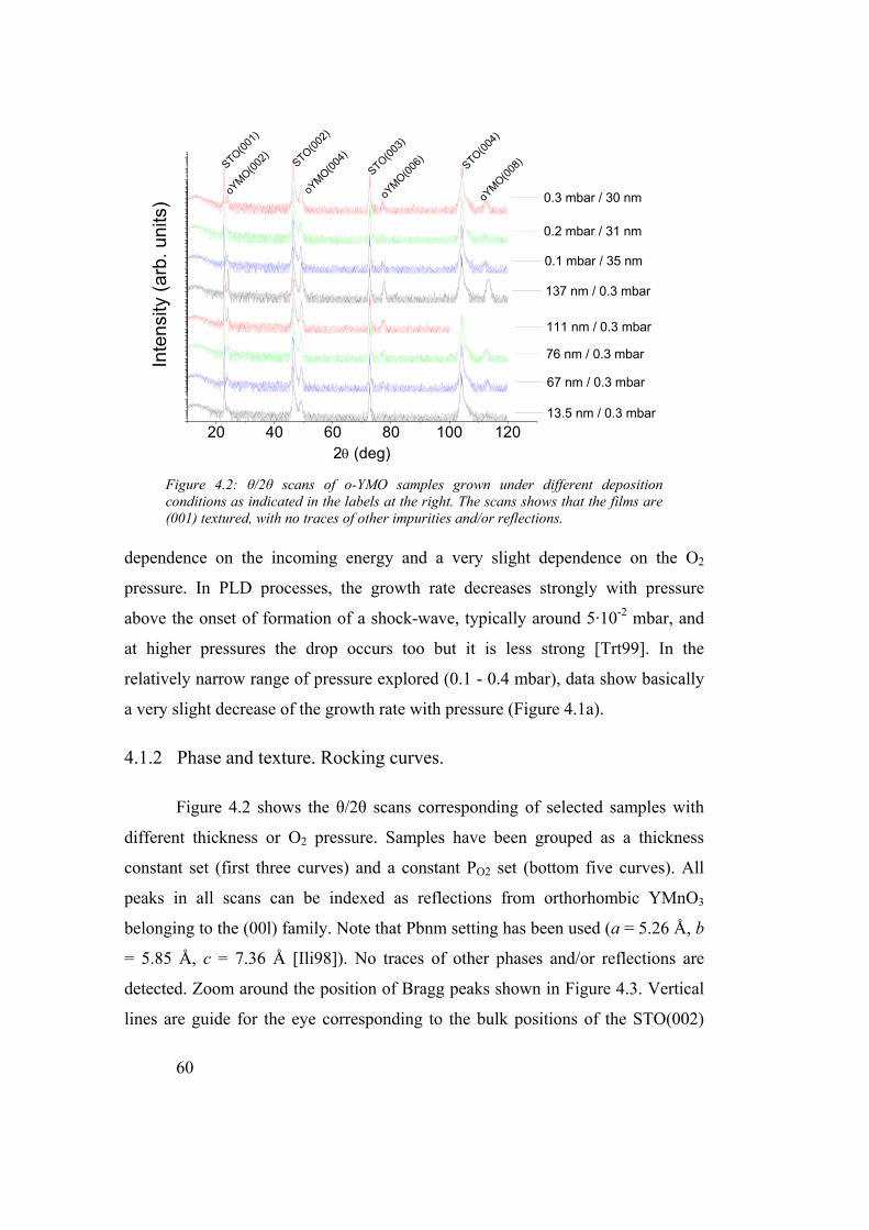
60
20 40 60 80 100 120 13.5 nm / 0.3 mbar
2θ (deg)
67 nm / 0.3 mbar
76 nm / 0.3 mbar
111 nm / 0.3 mbar
137 nm / 0.3 mbar
Inte
nsity
(arb
. uni
ts)
0.1 mbar / 35 nm
0.2 mbar / 31 nm
oYMO(00
8)
oYMO(00
6)
oYMO(00
4)
oYMO(00
2)STO(001)
STO(004)
STO(003)
0.3 mbar / 30 nm
STO(002)
Figure 4.2: θ/2θ scans of o-YMO samples grown under different deposition conditions as indicated in the labels at the right. The scans shows that the films are (001) textured, with no traces of other impurities and/or reflections.
dependence on the incoming energy and a very slight dependence on the O2
pressure. In PLD processes, the growth rate decreases strongly with pressure
above the onset of formation of a shock-wave, typically around 5·10-2 mbar, and
at higher pressures the drop occurs too but it is less strong [Trt99]. In the
relatively narrow range of pressure explored (0.1 - 0.4 mbar), data show basically
a very slight decrease of the growth rate with pressure (Figure 4.1a).
4.1.2 Phase and texture. Rocking curves.
Figure 4.2 shows the θ/2θ scans corresponding of selected samples with
different thickness or O2 pressure. Samples have been grouped as a thickness
constant set (first three curves) and a constant PO2 set (bottom five curves). All
peaks in all scans can be indexed as reflections from orthorhombic YMnO3
belonging to the (00l) family. Note that Pbnm setting has been used (a = 5.26 Å, b
= 5.85 Å, c = 7.36 Å [Ili98]). No traces of other phases and/or reflections are
detected. Zoom around the position of Bragg peaks shown in Figure 4.3. Vertical
lines are guide for the eye corresponding to the bulk positions of the STO(002)

61
40 45 50 5513.5 nm / 0.3 mbar
2θ (deg)
67 nm / 0.3 mbar
76 nm / 0.3 mbar
111 nm / 0.3 mbar
137 nm / 0.3 mbar
Inte
nsity
(arb
. uni
ts)
0.1 mbar / 35 nm
0.2 mbar / 31 nm
oYMO(00
4)
0.3 mbar / 30 nmSTO(00
2)
Figure 4.3: (a) Detail of the θ/2θ scans showed in Figure 4.2 Vertical lines correspond to the bulk position of STO(002) and oYMO(004). The shift in the position of the oYMO(004) peak indicates that the films are more relaxed as the thickness increases and that there is an small PO2 dependence.
and oYMO(004). Data show that the diffraction peaks from the film are closer to
the bulk positions when the thickness is larger or when they are grown at larger
PO2. This fact suggests that more strained films can be obtained by reducing PO2
and the thickness.
Rocking curves of the o-YMO(004) reflection for the samples grown at a
constant pressure indicate an slight increase of the FWHM with the thickness
from Δω = 0.30º in the 27 nm thick sample up to Δω = 0.45º at 137 nm (Figure
4.4). Note that the height of the peaks has been normalized in Figure 4.4. As a
reference, the rocking curve of the STO(002) substrate reflection is shown in the
inset of Figure 4.4. The substrate’s FWHM of the (002) reflection is 0.08 º. Our
FWHM values for the film are comparable to the obtained with the similar
compounds YbMnO3 (0.28 º for a 39 nm thick film) [Rub08] and HoMnO3 (0.61 º
for a 202 nm thick film) [Lin09], but clearly larger than the smaller values
reported by Hsieh et al. for YMnO3 (0.06 º for a films thicker than 180 nm)
[Hsi08] grown on SrTiO3(001) under similar PLD growth conditions.
In order to investigate the presence of spurious manganese oxides in the
samples using laboratory equipments we have performed long acquisition time

62
-2 -1 0 1 20.00
0.25
0.50
0.75
1.00
-0.15 0.00 0.15
YMnO3 137 nm 67 nm 27 nm
Inte
nsity
(cou
nts)
Δω (deg)
Δω (deg)
STO
Figure 4.4: Rocking curves of the (004) oYMO reflection for three samples grown at 0.3 mbar showing a small increase in the FWHM as thickness increases.
2θ
ψSTO(002)YMO(004)
(a)(b)
2θ
ψ
(021)f
(111)f
(112)f(110)STO
Figure 4.5: (a) X-ray diffraction θ/2θ scan performed with area detector taken in 7000 s. (b) Integrated intensity of all ϕ-frames after a pole figure. Only reflections regarding to the o-YMO are observed. Sample: 0.1 mbar / 119 nm.
(7000 s) measurements in the range of θ/2θ (28 – 60 º) which contains the most
intense peaks of most common Mn oxides (for instance, the most intense peak of
Mn3O4 is located at 2θ = 36.62 º [Mor03]).
Data are shown in Figure 4.5a. Only peaks from the oYMO(004) and
STO(002) were observed, as well as the tiny Kβ of STO(002) – note that the Ni
filter was not used to get the maximum count rate. Possible spurious contributions
could also present reflections located at angular positions not included in the scan

63
in Figure 4.5a. To this end, we performed the scan in Figure 4.5a tilting Ψ ~ 45 º
and rotating ϕ from 0 º to 360 º during a 5 hour measurement. The resulting Ψ-θ
frame shown in Figure 4.5b did not reveal any unexpected reflection or traces of
polycrystalline material.
4.1.3 Epitaxial relationship and crystal domain structure
In section 4.1.2, I have shown that o-YMO/STO(001) films are c-oriented.
Therefore, a (in bulk, 5.26 Å) and b (in bulk, 5.85 Å) are the lattice parameters
which have to match the STO(001) substrate (aSTO = 3.905 Å). Cube on cube
growth is not, in principle, possible since the lattice mismatch, calculated as
f = 100 · (aSTO - aYMO) / aYMO), would be larger than 25 %. In contrast, if o-YMO
is accommodated 45º in-plane rotated with respect to the [100]STO direction, then
the lattice parameters have to match on the STO diagonal (√2 · 3905 Å = 5.523 Å)
which is significantly closer to the o-YMO in-plane lattice parameters. Two
different scenarios can take place as shown in Figure 4.6. Firstly, if the diagonal
of o-YMO is clamped to the [100] or [010] direction of the substrate (panels a and
b) or, secondly, if o-YMO[100] and o-YMO[010] directions are parallel to the
[110]STO direction (panel c). Since the [100]STO and [010]STO in-plane
directions are equivalent, 4 and 2 in-plane crystal domains are expected in the first
and second case, respectively. Lattice mismatch corresponding to both situations
is presented in Table 4.2.
Figure 4.6 (a and b) Figure 4.6 (c)
STO parameter (Å)
oYMO parameter (Å) 2 · 3.905 Å = 7.810 Å √2 · 3.905 Å = 5.523 Å
a = 5.26 Å f[100] = 4.99 %
b = 5.85 Å f[010] = - 5.60 %
√(5.262 + 5.852) = 7.86 Å f[110] = - 0.72 % Table 4.2: Lattice mismatches corresponding to the scenarios sketched in Figure 4.6
According to the quantitative values in Table 4.2, the situation depicted in
panels a and b of Figure 4.6 may seem clearly favourable. However, the growth of
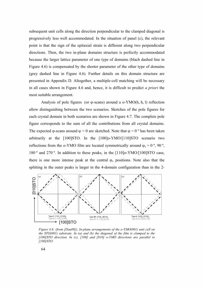
64
[100]STO
[010
]STO
Figure 4.6: (from [Dau09]). In-plane arrangements of the o-YMO(001) unit cell on the STO(001) substrate. In (a) and (b) the diagonal of the film is clamped to the [100]STO direction. In (c), [100] and [010] o-YMO directions are parallel to [100]STO.
subsequent unit cells along the direction perpendicular to the clamped diagonal is
progressively less well accommodated. In the situation of panel (c), the relevant
point is that the sign of the epitaxial strain is different along two perpendicular
directions. Then, the two in-plane domains structure is perfectly accommodated
because the larger lattice parameter of one type of domains (blach dashed line in
Figure 4.6) is compensated by the shorter parameter of the other type of domains
(grey dashed line in Figure 4.6). Further details on this domain structure are
presented in Appendix D. Altogether, a multiple-cell matching will be necessary
in all cases shown in Figure 4.6 and, hence, it is difficult to predict a priori the
most suitable arrangement.
Analysis of pole figures (or ϕ-scans) around a o-YMO(h, h, l) reflection
allow distinguishing between the two scenarios. Sketches of the pole figures for
each crystal domain in both scenarios are shown in Figure 4.7. The complete pole
figure corresponds to the sum of all the contributions from all crystal domains.
The expected φ-scans around ϕ = 0 are sketched. Note that ϕ = 0 º has been taken
arbitrarily at the [100]STO. In the [100]o-YMO/[110]STO scenario two
reflections from the o-YMO film are located symmetrically around ϕc = 0 º, 90 º,
180 º and 270 º. In addition to these peaks, in the [110]o-YMO/[100]STO case,
there is one more intense peak at the central ϕc positions. Note also that the
splitting in the outer peaks is larger in the 4-domain configuration than in the 2-

65
[100]STOϕ = 0 º
4 domains: [110]o-YMO/[100]STO
2 domains: [100]o-YMO/[110]STO
-10 -5 0 5 100.00
0.25
0.50
0.75
1.00
Inte
nsity
(arb
. uni
ts)
ϕ (deg)
ϕc
2domains
-10 -5 0 5 10
4domains
ϕ (deg)
Figure 4.7: Sketch of the pole figures corresponding to each crystal domain depicted in Figure 4.6. In the first case, the unit cell diagonal follows the [100] or [010] substrate directions. In the second case, the unit cells are rotated 45º respect the [100]STO direction. Plots present the expected φ-scan around φ = 0 º for both situations.
0 90 180 270 360ϕ (deg)
0.1 mbar / 119 nm
0.2 mbar / 31 nm
Inte
nsity
(arb
. uni
ts)
o-YMO(111)0.3 mbar / 76 nm
STO(111) Δϕ ≈ 5.5 º
170 180 190 ϕ (deg)
ϕc
Figure 4.8: ϕ-scans of the o-YMO(111) and STO(111) reflections. The splitting in the o-YMO peaks and the position of the substrate peaks indicate that the epitaxial relationship is the [100]o-YMO/[110]STO and [010]o-YMO/[110]STO.
domains case.
Data corresponding to the ϕ-scan of the oYMO(111) reflection for a set of
samples are shown in Figure 4.8. Data shows the clear splitting of the peaks at ϕc
irrespective of the PO2 and thickness with no intense central peak observed. A
zoom around 180 º is presented at the right for the three samples. The peaks can

66
be fitted by two Gaussian contributions as shown.
Therefore, the epitaxy corresponds to the two crystal domain scenario with
the following epitaxial relationships for each of the two crystal domains:
[100]o-YMO(001) // [110]STO(001) and [010]o-YMO(001) // [110]STO(001). In
this scenario, the expected splitting of the peaks using the bulk parameters is
Δϕbulk-2 = atan(a/b) – atan(b/a) = 6.08 º. The measured splitting in Δϕ is slightly
smaller than Δϕbulk indicating an a/b ratio closer to unity in thin films than in bulk;
however, from these measurements the accuracy is not high enough as to extract
trends and/or conclusions on the in-plane lattice parameters. It is worth
commenting that the expected splitting in the four domain configuration (that is,
the clamped-diagonal arrangement) is Δϕbulk-4 = 2·[atan(a/b) – atan(b/a)] = 12.16 º
which is clearly not supported by our experimental data. Just to mention that o-
YMO(111) reflection has been selected for its large intensity and for the lack of
overlapping with any other reflection from the substrate. This is particularly a
critical point because the substrate reflections are usually located at ϕc and could
lead to confusion.
4.1.4 Reciprocal space mapping
Reciprocal space maps (RSM) were performed in order to determine the
lattice parameters and the epitaxial strain of the thin films. According to the
epitaxial relationship and the crystal domain structure, the STO(h=k, h=k, l), o-
YMO(2h, 0, 2l) and o-YMO(0, 2h, 2l) reflections are contained in the same ϕ
angle slab and are suitable for RSM. Since a reflection from the substrate is
required near the film diffraction spots to correct small angle misalignments, only
two regions are suitable: around STO(113) or STO(114). Scans were performed in
the latter region as intensities recorded for the film’s (208) and (028) peaks were
found to be larger.
Figure 4.9 shows the RSM for a set of samples grown at the same oxygen
pressure (0.3 mbar) but with different thickness. In panel (a) are labelled the two
spots corresponding to the film’s reflections (028) and (208) as well as the
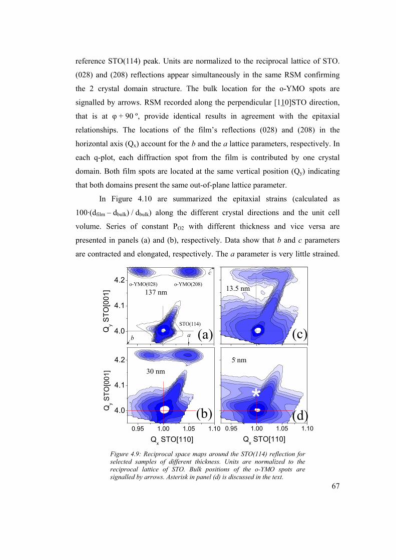
67
4.0
4.1
4.2c
b
o-YMO(208)o-YMO(028)
Qy S
TO[0
01]
STO(114)
a
0.95 1.00 1.05 1.10
4.0
4.1
4.2
Qx STO[110]
Qy S
TO[0
01]
0.95 1.00 1.05 1.10
Qx STO[110]
(a)
(b)
(c)
(d)
137 nm
30 nm
13.5 nm
5 nm
*
Figure 4.9: Reciprocal space maps around the STO(114) reflection for selected samples of different thickness. Units are normalized to the reciprocal lattice of STO. Bulk positions of the o-YMO spots are signalled by arrows. Asterisk in panel (d) is discussed in the text.
reference STO(114) peak. Units are normalized to the reciprocal lattice of STO.
(028) and (208) reflections appear simultaneously in the same RSM confirming
the 2 crystal domain structure. The bulk location for the o-YMO spots are
signalled by arrows. RSM recorded along the perpendicular [110]STO direction,
that is at φ + 90 º, provide identical results in agreement with the epitaxial
relationships. The locations of the film’s reflections (028) and (208) in the
horizontal axis (Qx) account for the b and the a lattice parameters, respectively. In
each q-plot, each diffraction spot from the film is contributed by one crystal
domain. Both film spots are located at the same vertical position (Qy) indicating
that both domains present the same out-of-plane lattice parameter.
In Figure 4.10 are summarized the epitaxial strains (calculated as
100·(dfilm – dbulk) / dbulk) along the different crystal directions and the unit cell
volume. Series of constant PO2 with different thickness and vice versa are
presented in panels (a) and (b), respectively. Data show that b and c parameters
are contracted and elongated, respectively. The a parameter is very little strained.

68
0.96
0.98
1.00(b)
Vol
ume
/ Bul
kPO2 = 0.3 mbar(a)
110 - 140 nm 30 nm
-0.5
0.0
0.5
ε [100
] (%
)
0
-2
-4
ε [010
] (%
)
0 20 40 60 80 100 120 1400.0
0.5
1.0
ε [001
] (%
)
Thickness (nm)0.0 0.1 0.2 0.3 0.4
PO2 pressure (mbar)
Figure 4.10: Unit cell volume and lattice strain in the o-YMO/STO(001) samples as a function of (a) the thickness and (b) the PO2 pressure during deposition. Lines are guides for the eye.
From the unit cell matching picture shown in Figure 4.6c, it turns out that the
longer in-plane lattice parameter (b = 5.85 Å) has contracted aiming to match the
substrate (√2·aSTO = 5.52 Å). In contrast, the shorter in-plane parameter (a = 5.26
Å) has remained almost fully relaxed. Since |5.85 – 5.52| > |5.26 – 5.52|, it is
reasonable to expect that the lattice parameter with larger mismatch with the
substrate would be the one presenting larger changes. In this situation, the out-of-
plane parameter is expected to increase in order to keep the unit cell volume
constant after the reduction of the surface ab.
The thickness series will be discussed in deeper detail now. Regarding the
in-plane parameters, as the thickness decreases, the two spots corresponding to the
in-plane o-YMO parameters get progressively closer to Qx = 1 (Figure 4.9). That
is, they display a tendency towards the substrate in-plane parameters as thickness
reduces. The b parameter presents larger variations in contrast to the a parameter

69
which does not display any thickness dependence and remains essentially fully
relaxed. Regarding the vertical axis, there is a reduction of the Qy with the sample
thickness indicating that the c parameter is gradually elongated until an abrupt
change in the thinnest sample.
On the other hand, samples grown with different PO2 present a subtle
relaxation as pressure increases in the 0.1 – 0.3 mbar range. Inspection of Figure
4.10 reveals that the changes in the epitaxial strain in b are approximately two
times larger than the changes in c. Also, the unit cell volume is not notably
expanded when the PO2 pressure is reduced. Although the presence of oxygen
vacancies cannot be discarded on the basis of these observations, it seems that
they don’t play a major role on the observed variation of the unit cell parameters.
Indeed it is typically found that oxygen vacancies expand the unit cell volume.
The structural differences between the films grown at different PO2 may be related
to the lower growth rates which are found at higher PO2 (Figure 4.1a). In that case,
the less amount of adatoms reaching the film surface on each pulse would allow a
larger relaxation of the unit cell parameters.
To conclude, results indicate that changing sample thickness and PO2
pressure allow obtaining a set of gradually strained epitaxial thin films. In
particular, sample thickness is found to be the optimal parameter to obtain a wider
gradual spread of unit cell volumes and strains along the [010] direction.
Domain structure in very thin samples (t = 13.5 nm and 5 nm)
As shown in Figure 4.9, samples with thickness larger than 13.5 nm
display a well defined separated two diffraction spots as expected for the 2 crystal
domain structure. These spots become clearly closer in the 13.5 nm thick film and,
in the 5 nm thick film, the two spots are no longer visible. However, there is a
small diffracted intensity centred roughly at Qx ~ 1 and Qy ~ 4.08 as signalled by
an asterisk in the figure. This suggests that the 5 nm thick sample is highly
strained presenting almost a coherent growth with the substrate. However, the
lattice parameters and whether there are one or two peaks (crystal domains) are
difficult questions to be answered by means of the current q-plot because of the

70
YMO(024): b
YMO(204): a STO(112)
(300 s)t = 30 nmt = 5 nm
STO(002)
(a) (b)
(3000 s)
1.8 1.9 2.0 2.1 2.2
o-YMO(004)
Inte
nsity
(arb
. uni
ts)
L
λ = 0.681 Å
STO(002)
Figure 4.11: (a) 3000 s frame taken around the STO(002) reflection in the 5 nm thick sample. No clear contribution from the film was detected. Inset shows a θ/2θ scan performed with synchrotron light (Spline, Grenoble). (b) Example of the θ-Ψ plot to investigate the presence of crystal domains in reflections with low L index.
overlapping of the substrate peak.
The amount of crystal domains could be investigated by measuring RSM
around intense enough film’s reflections far from any substrate peak. In the
standard RSM procedure (Ψ = 0) this is rather difficult because, on one hand, the
most intense o-YMO (h0l) reflections usually lay below the accessible reciprocal
space and, on the other hand, the lower the l Miller index, the closer the film and
the substrate reflections. If Ψ ≠ 0 is allowed, the more intense (204) and (024) o-
YMO reflections can be collected together as well as the substrate reflection
STO(112) in one single frame in a 2-D detector. An example for the 30 nm
sample is shown in Figure 4.11b. For the 5 nm thick sample only the STO
contribution was observed. It would be then interesting to monitor o-YMO
reflections such as (203) (the most intense in o-YMO) which are not accompanied
by a nearby substrate peak. However, the intensity of (203) is lower than in the
(204) reflections and are not expected to be better detected.
An abnormally large c parameter could not be confirmed by laboratory-
standard θ/2θ XRD experiments. However, a shoulder in the substrate STO(002)
reflection has been observed using synchrotron light (Spline-ESRF) indicating c ~
7.60 Å, that is Qy ~ 4.12 r.l.u (inset in Figure 4.11a). This value is visibly different

71
nm
0
2
4
6
8
10
12
14
16
18
100 nm 100 nm
(a) (b)
Figure 4.12: AFM topographic images of o-YMO films grown at 0.2 mbar with thickness (a) a 31 nm and (b) 122 nm. Results of the counting algorithm performed in the topography map are shown in the inset. Crosses signal each counted grain.
from the estimated position by the reciprocal space map in Figure 4.9d. However,
the determination of the central value of Qy is subject to a significant uncertainty
as well as the determination of the center of the shoulder in Figure 4.11. Clearly,
further attention must be paid on this issue. At the present time, in-plane
diffraction experiments are programmed.
4.1.5 Microstructural characterization
The crystal domain structure discussed in section 4.1.3 helps releasing the
excess of elastic energy due to the epitaxial strain observed in the strained o-YMO
films. In similar orthorhombic TbMnO3 [Dau09b] and YbMnO3 [Rub08] strained
thin films, also grown on STO(001) substrates, the crystal domains have been
imaged by TEM. A columnar growth starting from the bottom of the substrate was
observed. It was also found that the density of domain walls was reported to
decrease with the increasing the film thickness [Dau09]. This observation is very
relevant since the microstructural disorder could be related with an eventual
magnetic disorder. The implications will be discussed later in this chapter.
The presence of domains and/or crystal defects introduces disorder in the
ideal epitaxial arrangement that is reflected on the surface morphology. Analysis
of the root mean square (RMS) surface roughness and grain density using atomic
force microscope allows the indirect monitoring the main trends of the

72
0.1 0.2 0.3
2
3
4
0
500
1000∼ 30 nm> 111 nm
RM
S (n
m)
PO2 (mbar)
(a)
0 50 100
∼ 30 nm> 111 nm(b)
Thickness (nm)
0.98 1.00
2
3
4(c)
RM
S (n
m)
Vc / bulk
Gra
ins
per μ
m2
Figure 4.13: RMS roughness dependence with the pressure at constant thickness (a) and with the thikcness (b). (c) RMS roughness and grain density versus the unit cell volume distortion. Lines are guide for the eye.
microstructure with the growth conditions and thickness.
All o-YMO films display grain-like pattern morphology with lateral grain
size in the 50-100 nm range. In figure 4.12 are shown two illustrative samples (31
and 119 nm thick; grown at PO2 = 0.2 mbar). Surface root mean square (RMS)
roughness and grain density have been investigated in a set of films grown at
different deposition conditions. Grain density has been measured by
MountainsMap SPM software and a visual example of the resulting data is shown
in the insets of Figure 4.12b.
Quantitative results are presented in Figure 4.13 for two sets of samples of
different thickness. It is observed that RMS roughness depends on the deposition
conditions (PO2, shown in panel a) and with the thickness (panel b). Since, in the
o-YMO films, thickness and epitaxial strain are strongly correlated (Figure 4.10),
it would be expected also a dependence of the RMS roughness and the grain
density versus the epitaxial strain. Indeed, Figure 4.13c shows that the more
strained films, the smallest RMS roughness. Similarly, the grain surface density
increases in the more relaxed films. On the basis of our previous assumption and
considering the limitations of the analysis by AFM, data would indicate that less
microstructural disorder (grain/domain boundaries, etc.) is present in the strained
films and it increases as films relax. Among possible interpretations, it could be
73
proposed that if at the grain boundaries the material could be more relaxed, then
thicker films would be expected to be more relaxed since in those films the
amount of grain boundaries is larger. It would be tempting to correlate the amount
of crystal domains with the grain density. However, as I mentioned, TEM imaging
has shown that larger crystal domains are present in thicker films [Dau09] thus
ruling out this possibility.
4.2 Electronic state characterization
XRD characterization concluded that although larger variations in the
epitaxial strain are achieved via modification of the thickness, tuning the PO2
during the deposition also allowed producing samples with similar thickness but
different strain. This could result from different kinetic growth conditions caused
by the background atmosphere during the growth, but also due to chemical off-
stoichiometry eventually associated to the different growth conditions. To get a
information about the relative role of these effects and eventually, to discriminate
among them, XPS analysis of some films was performed.
Mn 3s spectra taken on samples grown at PO2 ranging from 0.1 and 0.4
mbar are shown in Figure 4.14. It is well known that in manganites the energy
splitting ΔE3s between the high-spin and the low-spin final state configuration is
roughly proportional to the Mn formal valence, with a decrease of roughly 0.7 eV
per unitary decrease in valence. [Gal02]. However from Figure 4.14 it is evident
that samples grown at different pressure present the same exchange splitting, i.e.
the same oxidation sate of Mn. Moreover the value ΔE3s=5.5 eV is compatible
with the oxidation state 3+, as expected for stoichiometric YMnO3. [Zho84,
Gal02, Ber08]. A possible misbalance of oxygen stoichiometry should have
instead induced the presence of a certain amount of Mn4+ and/or Mn2+ atoms for
electrical charge compensation which, at the same time, would have been detected
as merging of the Mn 3s peaks or a larger splitting, respectively.
Similarly, the Mn 2p core level also exhibits certain features depending on
the valence state of the manganese. The position of the main peak (Mn 2p3/2) is

74
Mn3s0.4 mbar
0.3 mbar
Inte
nsity
(arb
. uni
ts)
0.2 mbar
100 95 90 85 80 75
0.1 mbar
Binding energy (eV)
Δ E3s = 5.5 eV
(a)
658 651 644 637
287 286 285 284 283
0.1 mbar 0.3 mbar
Inte
nsity
(arb
. uni
ts)
B.E. (eV)
Mn 2p
B.E. (eV)
C 1s(b)
Figure 4.14: X-ray photoelectron spectroscopy scans around the position of (a) Mn 3s and (b) 2p. Figure shows that the change in O2 pressure during deposit in the range 0.1 – 0.4 mbar does not introduce changes in the chemical state of Mn. Shake-up peaks are not observed in Mn 2p core level. Inset shows the C 1s peak.
approximately at 640.2 eV if the oxidation state is 2+, at 641.4 eV if the oxidation
state is 3+ and at 642.6 eV for the 4+ oxidation state. There is a constant splitting
respect to the Mn 2p1/2 peak of around 11.8 eV [Gill99, Ber06]. In the case of 2+
oxidation state, there is an additional peak (shake-up) at 647 eV (signalled by
arrow). The Mn 2p region of samples grown at 0.1 and 0.3 mbar were
investigated. The XPS spectra did not display visible differences between the
samples. The shake-up peaks were not observed discarding a predominant Mn 2+
oxidation state. The location of the main peak, after background removal, is not
conclusive to discriminate among the Mn3+ and Mn4+ oxidation states.
Therefore, within the experimental resolution, the oxygen pressure during
the deposition has no influence on the chemical state of the Mn atoms located at
the surface.
4.3 Magnetic characterization
4.3.1 Background on bulk YMnO3 magnetic characterization
In order to understand the effect of the epitaxial strain on the magnetic
properties of thin films, the comparison with a reference having a relaxed lattice is
75
required. As we mentioned in Chapter 2, o-YMO is metastable and it has been
only obtained by high pressure synthesis and chemical routes. Due to this, there
are few reports on the magnetic properties of bulk o-YMO.
It seems that all studies agree that magnetic order-disorder transition takes
place at about 40 K (see chapter 2). However, this transition reflects in the
reported magnetization data in a very different way across the literature. While a
sharp kink in the temperature dependence of dc-susceptibility is observed at the
transition in Ref. [Lor04] there is only a very subtle bump on the data reported in
Ref. [Muñ02]. While the inverse susceptibility approaches the transition in a way
signaling ferrimagnetic order in Ref. [Bri97], this ferrimagnetic downturn is
absent in the data reported in Refs. [Muñ02, Ili05]. The low temperature data are
also rather different. While the susceptibility in Refs. [Lor04, Ili05] sharply
decreases below the transition and becomes a constant below 10 K, it increases all
the way down in Ref. [Muñ02]. It is worth mentioning that the field dependence
of magnetization is only reported by Muñoz et al. [Muñ02] and, as expected,
neither spontaneous magnetization nor hysteresis was observed at any temperature
down to 2 K. Finally, no single crystals from the orthorhombic phase of YMnO3
or similar manganites with E-type antiferromagnetic structure have been produced
yet. Therefore, there is no literature background on the magnetic anisotropy in
bulk samples.
4.3.2 Magnetic properties of relaxed thin films
Films with fully relaxed lattice parameters are expected to display the
bulk-like antiferromagnetic features such as no spontaneous magnetization and
the characteristic upturn at TN in the inverse susceptibility versus temperature
scans. Within the set of samples listed in Table 4.1, the most relaxed samples
were grown at 0.3 mbar with thickness above 110 nm.
Figure 4.15a shows the temperature dependence of the magnetization at
three relatively large high fields applied in-plane for the 145A sample (PO2 = 0.3
mbar, t = 111 nm, VC = 0.990·Vbulk). Raw data have been treated as described in

76
0 50 100 150 200 250 3000
1
2
3
4
5M
(em
u/g)
Temperature (K)
20 kOe 15 kOe 10 kOe
(a)
FC, H // [100]o-YMO
-50 0 50 100 150 200 250 3000
5
10
15
20FC, H // [100]o-YMO
1/χ
(kO
e / e
mu/
g)
Temperature (K)
20 kOe 15 kOe 10 kOe
(b)
TN
Vc = 0.990·Vbulk
Figure 4.15: (a) Magnetization versus temperature curves for an almost fully relaxed sample (145; PO2 = 0.3 mbar, 111 nm). AF-like cusp is found at T = 40 K. (b) 1/χ curves merge at the paramagnetic regime. Solid line is guide for the eye with the expected slope of Mn 3+ in the paramagnetic regime.
0 50 100 150
-1.25
-1.00
-0.75
-0.50
(a)
FC ZFC
M (1
0-6 e
mu)
Temperature (K)
0 5 10 15 20
-10
-5
0
-1 0 1-1
0
1
(b)M (1
0-5 e
mu)
Field (kOe)
T = 20 K
M (1
0-5 e
mu)
Field (kOe)
Figure 4.16: (a) reversible ZFC-FC magnetization for an almost fully relaxed sample (145; PO2 = 0.3 mbar, t = 111 nm). (b) Magnetization loops at T = 20 K < TN show no remanent magnetization.
Appendix C in order to remove the substrate and eventual saturated ferromagnetic
impurities in all the temperature range.
A clear AF-like cusp appears at TN = 40 K followed by a drop of
magnetization as expected for antiferromagnetic behavior. In Figure 4.15b are
shown the inverse susceptibility plots of the former curves. Remarkably the three
curves merge in the paramagnetic regime and display the mentioned
antiferromagnetic-like upturn signaling TN ~ 40 K. The solid line is a guide for the
eye indicating the nominal slope for the Mn3+ oxidation state. Therefore, the Mn
in the film is Mn3+ in agreement with the XPS measurements. The linear regime
extrapolates to θp = - 30 K indicating that the Mn-O-Mn interactions are
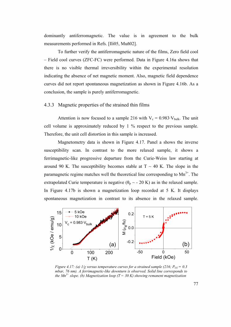
77
0 100 2000
5
10
15
Vc = 0.983·Vbulk
1/χ
(kO
e / e
mu/
g)
T (K)
5 kOe 10 kOe
(a)
-50 0 50
-0.2
0.0
0.2
(b)
M (μ
B/fu
)
Field (kOe)
T = 5 K
Figure 4.17: (a) 1/χ versus temperature curves for a strained sample (216; PO2 = 0.3 mbar, 76 nm). A ferrimagnetic-like downturn is observed. Solid line corresponds to the Mn3+ slope. (b) Magnetization loop (T = 30 K) showing remanent magnetization
dominantly antiferromagnetic. The value is in agreement to the bulk
measurements performed in Refs. [Ili05, Muñ02].
To further verify the antiferromagnetic nature of the films, Zero field cool
– Field cool curves (ZFC-FC) were performed. Data in Figure 4.16a shows that
there is no visible thermal irreversibility within the experimental resolution
indicating the absence of net magnetic moment. Also, magnetic field dependence
curves did not report spontaneous magnetization as shown in Figure 4.16b. As a
conclusion, the sample is purely antiferromagnetic.
4.3.3 Magnetic properties of the strained thin films
Attention is now focused to a sample 216 with Vc = 0.983·Vbulk. The unit
cell volume is approximately reduced by 1 % respect to the previous sample.
Therefore, the unit cell distortion in this sample is increased.
Magnetometry data is shown in Figure 4.17. Panel a shows the inverse
susceptibility scan. In contrast to the more relaxed sample, it shows a
ferrimagnetic-like progressive departure from the Curie-Weiss law starting at
around 90 K. The susceptibility becomes stable at T ~ 40 K. The slope in the
paramagnetic regime matches well the theoretical line corresponding to Mn3+. The
extrapolated Curie temperature is negative (θp ~ - 20 K) as in the relaxed sample.
In Figure 4.17b is shown a magnetization loop recorded at 5 K. It displays
spontaneous magnetization in contrast to its absence in the relaxed sample.

78
Splitting in the ZFC-FC curves was observed below TN confirming this point; the
curves are presented later in this section.
Analysis of sample contamination
The detection of ferromagnetic Mn3O4 (Hausmannite) is very difficult
because its transition temperature (~ 42 K [Jen74, Tac07]) is very close to the o-
YMO AF ordering. On one hand, the presence of Mn3O4 (either polycrystalline or
epitaxial) has not been detected by careful XRD analyses such as the ones shown
in Figure 4.5. On the other hand, its eventual significant presence in the film
would imply the misbalance in the film stoichiometry, leading to changes in the
Mn oxidation state which has not been detected by neither XPS nor the slope in
1/χ the paramagnetic regime.
According to the measured saturation magnetization Ms ~ 0.23 μB/fu at 5
K of this sample (which is not the more ferromagnetic sample in the set) and the
reported values for Mn3O4 (1.8 μB/fu predicted in Ref. [Jen74] and 1.5 μB/fu
measured in Ref. [Tac07]) there should be more than 10 % of the film containing
spurious Mn3O4. Therefore, contrary to our experimental evidences its presence
should be detected by XRD and/or XPS spectroscopy (if it is located at the
surface).
Therefore, the magnetic properties in the strained sample (0.983·Vbulk) are
intrinsic. It turns out, that the increasing the epitaxial strain in the film a net
magnetic moment has been induced.
4.3.4 Magnetic anisotropy
In the simplest antiferromagnetic picture, a drop of magnetization should
occur at TN as temperature is reduced if the measurement is performed with the
magnetic field (H) applied along the antiferromagnetic axis. If H is applied
perpendicular to such axis, the magnetization should remain constant. If the
induced ferromagnetism in the films originates via a small distortion of the
antiferromagnetic structure, part of the features of the anisotropy of the
susceptibility of the antiferromagnetic response should remain visible.

79
0 25 50 75 100T (K)
M (e
mu)
μ0H//=0.02T
ZFC
FC
0 25 50 75 100T (K)
μ0Happl=0.1T
ZFC
FC
0 25 50 75 100
μ0H//=1T
T (K)
ZFC
FC(a) (b) (c)
0 25 50 75 100T (K)
M (e
mu)
μ0H⊥=0.05T
ZFC
FC
0 25 50 75 100T (K)
μ0H⊥=0.1T
ZFC
FC
0 25 50 75 100T (K)
μ0H⊥=1T
ZFC
FC(d) (e) (f)
H // [110]o-YMO(001)
H // [001]o-YMO(001)
c
b
c
b
Figure 4.18: ZFC-FC curves measured with the magnetic field applied in-plane (a-c) and out-of-plane (d-f) for the sample 210 (PO2 = 0.1 mbar, t =35 nm). Although both directions present net magnetic moment (thermal hysteresis), a marked AF-like magnetic anisotropy is observed compatible with a spin-canted scenario.
Now is described how de magnetic field is applied in the anisotropy
experiments following the sketch in Figure 4.18. As mentioned in Chapter 2,
below TN, the o-YMO spins order along the [010] direction which will be
subsequently considered as the antiferromagnetic axis. According to the epitaxial
relationship, this direction is contained in-plane of the thin films but, note that,
due to the geometry of the substrates (supplied cut along [100] and [010]
direction), in the in-plane measurements the magnetic field is applied at 45 º of the
antiferromagnetic axis. In contrast, in the out-of-plane measurements, the
magnetic field is applied perpendicular to the antiferromagnetic axis.
ZFC-FC curves for the most strained sample (210; PO2 = 0.1 mbar, 35 nm
thick) were measured at several applied magnetic fields applied in- and out-of-
plane. Data in Figure 4.18 show that ZFC-FC curves split at TN ~ 40 K. There is
an obvious thermal hysteresis which decreases with increasing the magnetic field
upon disappearing at about 1 T as expected for ferromagnetic behavior. This
clearly shows that the magnetic ordered state is not purely AF but has a significant

80
FM component present along the two measured directions.
Of relevance here is the evident magnetic anisotropy that resembles the
antiferromagnetic pristine structure. While the FC in-plane measurements show a
kink at TN, followed by a reduction of magnetization, the out-of-plane
measurements show a monotonic increase. The observed anisotropic response can
be understood by assuming that a small ferromagnetic component perpendicular
to [010] direction is superimposed to the pristine antiferromagnetic anisotropy.
This magnetic response could result from the canting away from the b axis of the
spins. Being so, the magnetization should be expected to continue increasing in
the perpendicular measurement because each magnetic domain formed at TN
could be canted either in the direction of the magnetic field or in the opposite. On
the other hand, susceptibility should display a decrease in the in-plane
measurements due to antiferromagnetic reordering of the spins in the ab plane.
Since the later measurements are performed at 45 º and not exactly along the
antiferromagnetic axis, some hysteresis should be also expected in the “in-plane”
measurements.
Single domain films with b aligned parallel to the sample sides would be
highly desirable to discriminate the parallel and perpendicular behaviours. Our
progress in the growth of such films is described in Appendix D. Very recently,
Hsieh et al. [Hsi08] reported measurement on single-domain strained YMO thin
films grown on LaAlO3(110). They observed that the kink in the FC susceptibility
is observed only along the b direction, whereas along a and c directions presents a
monotonic increasing behaviour and argued that such anisotropy could be
understood as a canting of the Mn sub-lattice. Although the establishment of the
“canting” scenario has to wait for direct supportive evidence from other
independent measurements, our data and the reported results point directly to it as
a cause of the observed ferromagnetic response in strained o-YMO films.
The average departure of the magnetic moment away from the b-axis
(canting angle) can be estimated from the measured spontaneous magnetization.
In an ideal antiferromagnetic structure it is zero, but a finite magnetization was
measured in our films in the absence of magnetic field. The canting angle

81
221 223 225 2270.0
0.5
1.0
1.5
Can
ting
angl
e (º
)
Unit cell volume (Å3)
YM
nO3
bulk
-4 -2 0 2 40
1
2
3
223.04 Å3
222.67 Å3 221.30 Å3
M (e
mu/
g)
H (kOe)
T = 5 K(a)
(c)
H↑[010]oYMO→θ
4μBMr
H↑[010]oYMO→θ
4μBMr
(b)
θ//+45º
θ// - 45º
H↑[010]o
YMO→
θ//+45º
θ// - 45º
H↑[010]o
YMO→
[010][001]
[100]
Strained
Relaxed
Figure 4.19: (a) zoom of M(H) loops showing the remanent magnetization for samples with different unit cell volume. (b) Sketch of the calculation of the canting angles. (c) Polar (solid circles) and azimuthal (empty circle) canting angles as a function of the unit cell volume.
corresponds to the angle that spins must tilt in order to obtain such spontaneous
magnetization (sketch Figure 4.19b). The in-plane (Mr//) and out-of plane (Mr)
spontaneous magnetizations will be used to compute the polar (θ//) and azimuthal
(θ) canting angles, respectively. Using that the magnetic moment of the Mn
atoms is 4 μB, the canting angles can be obtained by trigonometry:
⎟⎠⎞
⎜⎝⎛=
−⎟⎟⎠
⎞⎜⎜⎝
⎛ +=
⊥−⊥
−
4sin
º454
22sin
1
//1//
r
r
M
M
θ
θ Eq. 4.1
The canting angles should reduce when films become gradually relaxed if
the epitaxial strain is the driving force tilting the magnetic structure. Indeed, data
in Figure 4.19 supports this expectation. From measurements of the spontaneous
magnetization (Figure 4.19a), the in-plane canting angle was obtained using Eq.
4.1 and plotted in Figure 4.19c (solid circles). Data show a monotonic decrease as
the films become relaxed. The polar canting angle has been measured for the
sample with Vc = 223.04 Å3 (empty circle) and it is of the same order as the polar
angle.

82
0 100 200 3000
1
2
3
4(b)
χ (e
mu/
g/kO
e)
Temperature (K)
221.30 Å3 (0.1 mbar / 35 nm)
221.09 Å3 (0.2 mbar / 31 nm)
221.40 Å3 (0.3 mbar / 30 nm)
221.89 Å3 (0.4 mbar / 49 nm)
222.67 Å3 (0.3 mbar / 76 nm)
223.04 Å3 (0.1 mbar / 119 nm)
224.24 Å3 (0.3 mbar / 111 nm)
224.97 Å3 (0.2 mbar /122 nm)
FC, H// = 500 Oe
0 20 40 600.1
1 224.97 Å3
Temperature (K)
0.1
1 223.04 Å3
M (e
mu/
g) 0.1
1(a)
221.30 Å3
Vbulk = 226.47 Å3Vbulk = 226.47 Å3
Figure 4.20: (a) ZFC-FC curves showing larger irreversibility for more distorted unit cells. (b) FC susceptibility of samples grown at different deposition conditions showing a dramatic increase of χ as distortion increases. The Curie-Weiss paramagnetism is plotted as solid line as reference.
4.3.5 Ferromagnetism versus epitaxial strain
Former section has evidenced from magnetization loops that the canting
angle displayed a gradual increase with increasing strain. On the other hand, in
sections 4.3.2 and 4.3.3 it has been shown that an almost fully relaxed sample is
purely antiferromagnetic whereas ferromagnetic behaviour is present in a more
strained film. Now this correlation between ferromagnetism and epitaxial strain
will be investigated for a set of samples presenting increasing epitaxial strain.
Figure 4.20a shows the ZFC-FC curves of three selected samples with
increasing unit cell volume. Magnetization data show larger ZFC-FC splitting
and, thus, larger magnetic moment in the films with smaller unit cells. This trend
is followed by all other samples in the set and is in agreement with the trends in
the canting angles in Figure 4.19.
FC susceptibility curves were measured for the complete set of samples
grown under different deposition conditions and, thus, presenting different strain
states. Data is shown in Figure 4.20b. Symbols are labelled according to the unit
cell volume and the deposition conditions. As expected, the curves merge in the
region T > TN where the system becomes paramagnetic. In contrast, in the
magnetically ordered state, the measured χ can be up to 35 times larger than the
extrapolated Curie-Weiss paramagnetic response (shown as thick line). Note that
in antiferromagnetic systems the χ(T = TN) > χ(T < TN). It is observed that the FC

83
221 222 223 224 225 226 2270
1
2
3
4
(a)
χ 25 K
(em
u/g/
kOe)
Unit cell volume (Å3)
YMnO 3 bu
lk
0 1 2 3 40
250
500
750
1000
2.0
2.5
3.0
3.5
4.0(b)
Gra
ins
per μ
m2
χ25K
(emu/g/kOe)
:RM
S ro
ughn
ess
(nm
)
More ferromagnetic
Less ferromagnetic
More ferroagnetic
Figure 4.21: (a) Susceptibility at 25 K as a function of the unit cell volume. More distorted unit cells present an increased magnetic response. (b) Grain density and RMS roughness versus the magnetic response.
susceptibility at the plateau around 25 K can be used as a parameter to assess the
net magnetic moment: if χ(T = 25 K) is larger, the splitting is larger. Then, χ(T =
25 K) can be used to quantify the ferromagnetic response of the samples.
Of relevance here is that χ(T = 25 K) is larger for more strained unit cells.
In order to get a quantitative insight, the unit cell volume is chosen as the simplest
and most appropriate parameter to reflect all structural distortions and, then, it is
correlated with χ(T = 25 K). Data in Figure 4.21a show that the susceptibility and,
thus, the concomitant ferromagnetism are clearly correlated with the unit cell
distortion.
Finally, one may imagine the scenario where the crystal defects
(dislocations, etc), grain boundaries or even surface roughness, may be a source of
magnetic disorder and/or uncompensated spins (see for instance Ref. [Dau09]). To
address this issue, in Figure 4.21b is plotted χ(T = 25 K) against the grain density
and surface roughness (RMS) as determined by AFM for films prepared under
different conditions. Recall that different experimental conditions lead to different
surface roughness and grain density (Section 4.1.5). Data in Figure 4.21b indicate
that the ferromagnetic component is reduced when increasing the RMS. It
suggests that uncompensated spins at grain boundaries do not play a dominant
role on the total magnetic response of the film. Clearly, films having rougher
surfaces present reduced magnetic response.
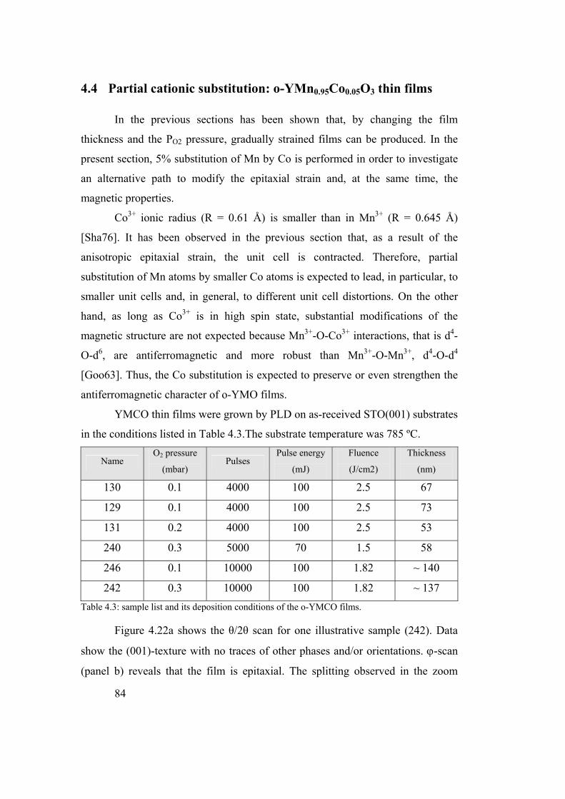
84
4.4 Partial cationic substitution: o-YMn0.95Co0.05O3 thin films
In the previous sections has been shown that, by changing the film
thickness and the PO2 pressure, gradually strained films can be produced. In the
present section, 5% substitution of Mn by Co is performed in order to investigate
an alternative path to modify the epitaxial strain and, at the same time, the
magnetic properties.
Co3+ ionic radius (R = 0.61 Å) is smaller than in Mn3+ (R = 0.645 Å)
[Sha76]. It has been observed in the previous section that, as a result of the
anisotropic epitaxial strain, the unit cell is contracted. Therefore, partial
substitution of Mn atoms by smaller Co atoms is expected to lead, in particular, to
smaller unit cells and, in general, to different unit cell distortions. On the other
hand, as long as Co3+ is in high spin state, substantial modifications of the
magnetic structure are not expected because Mn3+-O-Co3+ interactions, that is d4-
O-d6, are antiferromagnetic and more robust than Mn3+-O-Mn3+, d4-O-d4
[Goo63]. Thus, the Co substitution is expected to preserve or even strengthen the
antiferromagnetic character of o-YMO films.
YMCO thin films were grown by PLD on as-received STO(001) substrates
in the conditions listed in Table 4.3.The substrate temperature was 785 ºC.
Name O2 pressure
(mbar) Pulses
Pulse energy
(mJ)
Fluence
(J/cm2)
Thickness
(nm)
130 0.1 4000 100 2.5 67
129 0.1 4000 100 2.5 73
131 0.2 4000 100 2.5 53
240 0.3 5000 70 1.5 58
246 0.1 10000 100 1.82 ~ 140
242 0.3 10000 100 1.82 ~ 137 Table 4.3: sample list and its deposition conditions of the o-YMCO films.
Figure 4.22a shows the θ/2θ scan for one illustrative sample (242). Data
show the (001)-texture with no traces of other phases and/or orientations. ϕ-scan
(panel b) reveals that the film is epitaxial. The splitting observed in the zoom

85
(panel c) indicates the same crystal domain structure as in o-YMO films: two in-
plane crystal domains, 90º in-plane rotated, and the epitaxial relationships
[100]YMCO//[110]STO and [010]YMCO//[110]STO. The reciprocal space for two pairs
of samples grown under identical experimental conditions are shown in panels d
and e. In panel d the samples were grown at 0.3 mbar, while in panel e at 0.1
mbar. Plots show that o-YMCO peaks are not located in the bulk positions thus
indicating that the films are not relaxed. As in the o-YMO films, the epitaxial
strain is anisotropic being tensile along [001], compressive along [010] and
negligible along [100]. By comparing the location of the diffraction peaks of the
o-YMCO and o-YMO samples, it is observed that YMCO films display shorter b
and larger c parameters than YMO films of identical thickness. Since in the o-
YMO films the larger epitaxial strain is compressive in the [010] direction, it is
reasonable that the smaller Co atoms now allow a larger contraction of the b
parameter. Then the observed elongation of the c parameter should be expected.
Note that these trends are irrespective of the PO2. Moreover, the expected
contraction of the unit cell is confirmed. For instance, in the films prepared at 0.3
mbar, 223.19 Å3 and 224.37 Å3 are the unit cell volumes for the Co-doped and the
pristine o-YMO samples, respectively.
It is worth too comparing pairs of films (YMCO and YMO) presenting
similar unit cell volume. For instance, the lattice parameters for two pairs of
samples with similar unit cell volume are listed in Table 4.4.
Name PO2
(mbar)
Thickness
(nm)
a (Å)
± 0.01 Å
b (Å)
± 0.01 Å
c (Å)
± 0.01 Å
V (Å3)
± 0.65 Å3
I) 216 YMO 0.3 76 5.270 5.709 7.401 222.67
I) 129 YMCO 0.1 73 5.277 5.642 7.475 222.55
II) 141 YMO 0.1 119 5.255 5.722 7.417 223.04
II) 242 YMCO 0.3 137 5.253 5.713 7.437 223.18 Table 4.4: Deposition conditions, thickness, and lattice parameters for two pairs of YMO and YMCO samples presenting similar unit cell volume.
Data confirm that there is an effect due to the Co substitution: YMCO
films display shorter b and larger c parameters than YMO films with very similar
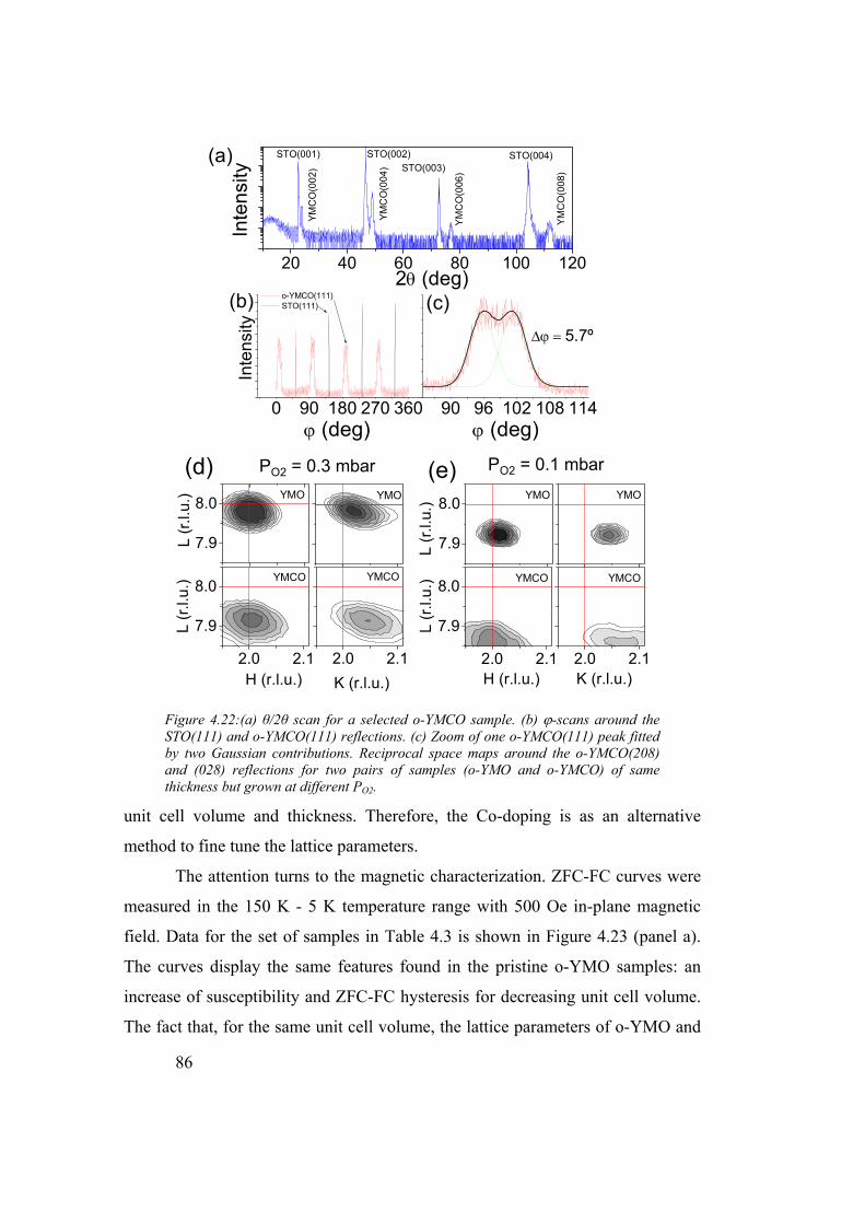
86
YMO
7.9
8.0
L (r
.l.u.
) YMO
2.0 2.1 K (r.l.u.)
YMCO
2.0 2.1
7.9
8.0
L (r.
l.u.) YMCO
H (r.l.u.)
YMO
2.0 2.1
7.9
8.0
L (r
.l.u.
) YMO
2.0 2.1
YMCO
K (r.l.u.)2.0 2.1
7.9
8.0
L (r
.l.u.
) YMCO
H (r.l.u.)
PO2 = 0.3 mbar PO2 = 0.1 mbar
20 40 60 80 100 120
(c)(b)
YMC
O(0
08)
YM
CO
(006
)
YM
CO
(004
)
YMC
O(0
02)
STO(004)STO(003)
STO(002)
Inte
nsity
2θ (deg)
STO(001)(a)
0 90 180 270 360
o-YMCO(111) STO(111)
Inte
nsity
ϕ (deg)90 96 102 108 114
ϕ (deg)
Δϕ = 5.7º
(d) (e)
Figure 4.22:(a) θ/2θ scan for a selected o-YMCO sample. (b) ϕ-scans around the STO(111) and o-YMCO(111) reflections. (c) Zoom of one o-YMCO(111) peak fitted by two Gaussian contributions. Reciprocal space maps around the o-YMCO(208) and (028) reflections for two pairs of samples (o-YMO and o-YMCO) of same thickness but grown at different PO2.
unit cell volume and thickness. Therefore, the Co-doping is as an alternative
method to fine tune the lattice parameters.
The attention turns to the magnetic characterization. ZFC-FC curves were
measured in the 150 K - 5 K temperature range with 500 Oe in-plane magnetic
field. Data for the set of samples in Table 4.3 is shown in Figure 4.23 (panel a).
The curves display the same features found in the pristine o-YMO samples: an
increase of susceptibility and ZFC-FC hysteresis for decreasing unit cell volume.
The fact that, for the same unit cell volume, the lattice parameters of o-YMO and

87
222 224 2260
2
4
5.6 5.7 5.8
7.35 7.40 7.45
0 50 100
0.25
0.50
0.75
1.00
1.25
1.50
221.99 Å3
222.55 Å3
222.82 Å3
223.34 Å3
223.19 Å3
(b)FC
ZFC
ZFC
FC
χ (e
mu/
g/kO
e)
T (K)
YMn0.95Co0.05O3(a)
YMOYMCOχ 25
K (e
mu/
g/kO
e)
Unit cell volume (Å3)
YMO bulk
bulk
χ 25 K
bulk
b (Å)
χ 25 K
c (Å)
Figure 4.23: (a) Susceptibility curves of YMCO films measured in FC conditions (at 500 Oe). ZFC branches are shown for two representative samples. Susceptibility at 25 K measured for o-YMO and YMCO films versus unit cell volume and lattice parameters.
nm
0
1
2
3
4
5
6
7
8
9
10
11
12(a) nm
0
1
2
3
4
5
6
7
8
9
10
11
12(a)
200 nm200 nm 0 1000 20000
1
2
3
4(b) o-YMO
YMCO
χ 25 K
(kO
e / e
mu/
g)
Grains per μm20 2 4
o-YMO YMCO (c)
RMS roughness (nm)
Figure 4.24: Susceptibility at 25 K versus (a) the grain density and (b) the surface RMS roughness for YMCO and YMO thin films.
o-YMCO samples are dissimilar can be used to investigate the role of the b and c
distances in the magnetic properties. χ(25 K) as a function of b and c are shown in
the inset of panel b for o-YMO and o-YMCO films. In both insets, a monotonic
increase of the susceptibility is observed as b shrinks or c increases indicating that
the more distortion, the more magnetic response.
But the most important result is that in χ(25 K) versus unit cell volume plot
(main panel), the o-YMCO samples exactly replicate the behaviour of o-YMO
films suggesting that the mechanism inducing the ferromagnetism is the same in
both cases. This similarity indicates that the observed ferromagnetism is not solely
determined, for instance, by the length of the b-axis but, most naturally, the

88
contribution of the modification of c (expansion) and a (constant) axis upon
epitaxial and chemical strain should be also included to get a measure of the
overall distortion of the unit cell. Data show that the unit cell volume is an
appropriate parameter for this purpose.
The correlation of the magnetic response with the surface morphology in
o-YMCO films was investigated. An AFM topographic image for a representative
sample (242) is shown in Figure 4.24a. A dense granular morphology is observed
like in o-YMO films. Then, if magnetic disorder at grain boundaries or rough
surfaces were relevant sources of net magnetization, one would expect χ25 to
increase with grain density and roughness. Data in Figure 4.24 (panels b and c)
indicate an opposite trend: both the RMS roughness and the grain density decrease
as the ferromagnetism increases for the Co-doped films. Therefore, surface and/or
interface disorder are not important sources of the observed ferromagnetism.
Co3+ spin state
In addition to the structural distortion caused by the Co substitution, the
magnetic properties could be modified due to a change in the Co atoms spin state.
If Co ions where in a low spin (LS) state, that is 3d6-Co3+ with S=0, the magnetic
interactions within the Mn sub-lattice would be diluted. As we mentioned, in
high-spin Co3+ (S=2) the antiferromagnetic interactions are preserved and changes
in the magnetic structure are not expected.
To investigate this issue trying to determine the spin state of the doping
Co3+, I have determined the slope in the 1/χ high temperature regime to determine
the effective paramagnetic moment of the film. To obtain a larger magnetic signal
in the paramagnetic region a thicker film (242; PO2 = 0.3 mbar, t = 137 nm) was
selected and measured at relatively high magnetic fields. Data are shown in Figure
4.25. Data reveal that in YMCO films the antiferromagnetic interactions are
dominating as it comes up from the negative extrapolated temperatures of
θp ~ - 20(5) K. After the corrections indicated in Appendix C, from the slope of
the linear part of 1/χ (T) in Figure 4.25 an effective moment μeff ≈ 5.0(3) μB can
be estimated. This value is quite close to that expected for high-spin Co3+ and
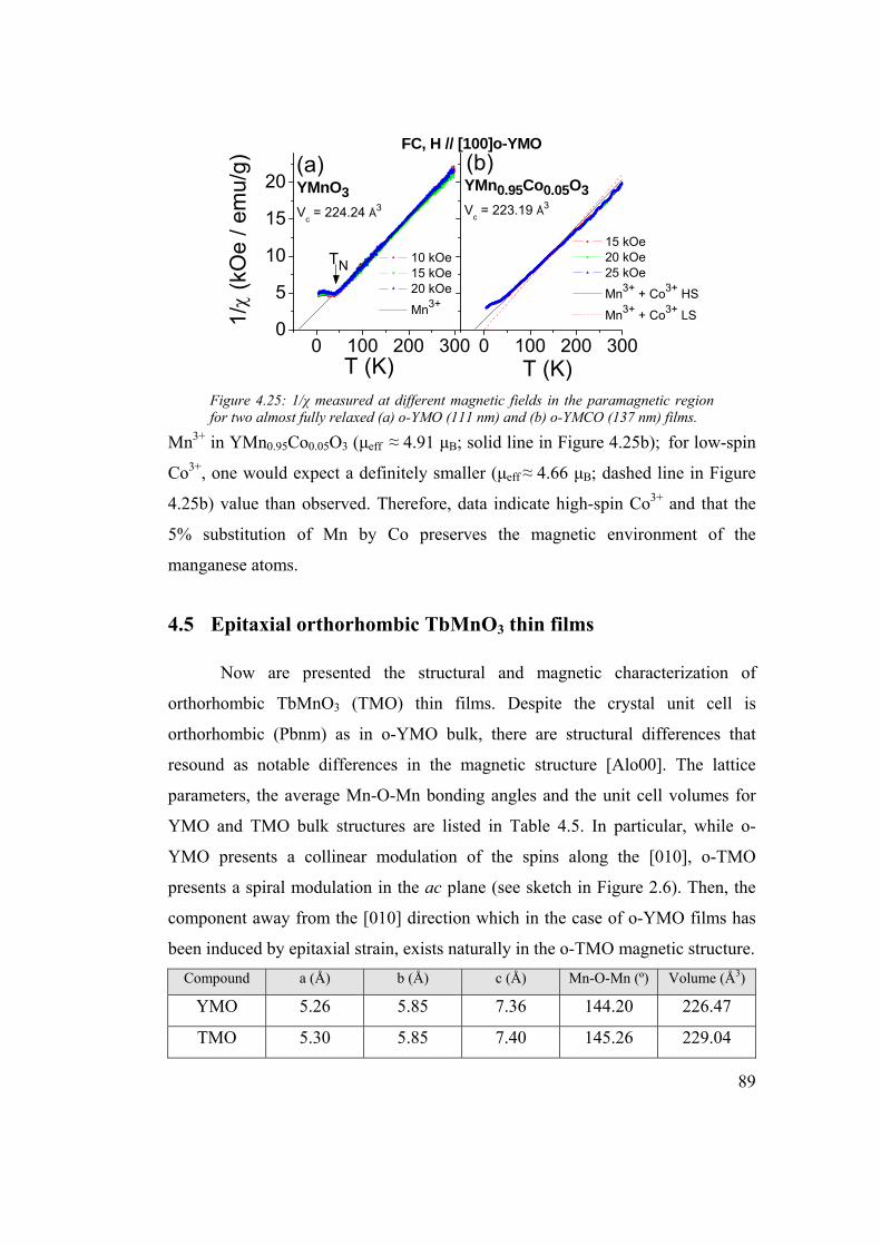
89
0 100 200 3000
5
10
15
20
0 100 200 300
(b)FC, H // [100]o-YMO
1/χ
(kO
e / e
mu/
g)
T (K)
10 kOe 15 kOe 20 kOe
Mn3+
(a)
TN
YMnO3Vc = 224.24 Å3
T (K)
15 kOe 20 kOe 25 kOe
Mn3+ + Co3+ HS
Mn3+ + Co3+ LS
YMn0.95Co0.05O3Vc = 223.19 Å3
Figure 4.25: 1/χ measured at different magnetic fields in the paramagnetic region for two almost fully relaxed (a) o-YMO (111 nm) and (b) o-YMCO (137 nm) films.
Mn3+ in YMn0.95Co0.05O3 (μeff ≈ 4.91 μB; solid line in Figure 4.25b); for low-spin
Co3+, one would expect a definitely smaller (μeff ≈ 4.66 μB; dashed line in Figure
4.25b) value than observed. Therefore, data indicate high-spin Co3+ and that the
5% substitution of Mn by Co preserves the magnetic environment of the
manganese atoms.
4.5 Epitaxial orthorhombic TbMnO3 thin films
Now are presented the structural and magnetic characterization of
orthorhombic TbMnO3 (TMO) thin films. Despite the crystal unit cell is
orthorhombic (Pbnm) as in o-YMO bulk, there are structural differences that
resound as notable differences in the magnetic structure [Alo00]. The lattice
parameters, the average Mn-O-Mn bonding angles and the unit cell volumes for
YMO and TMO bulk structures are listed in Table 4.5. In particular, while o-
YMO presents a collinear modulation of the spins along the [010], o-TMO
presents a spiral modulation in the ac plane (see sketch in Figure 2.6). Then, the
component away from the [010] direction which in the case of o-YMO films has
been induced by epitaxial strain, exists naturally in the o-TMO magnetic structure. Compound a (Å) b (Å) c (Å) Mn-O-Mn (º) Volume (Å3)
YMO 5.26 5.85 7.36 144.20 226.47
TMO 5.30 5.85 7.40 145.26 229.04

90
Table 4.5: lattice parameters, bonding angles and unit cell volumes of TMO and YMO bulk structures from Refs. [Che07b] and [Ili98], respectively.
Like in o-YMO, it is reasonable to expect also that epitaxial strain could
modify the magnetic topology and, thus, the magnetic properties in the o-TMO
films. To investigate this issue, the same methodology that has been developed for
o-YMO and o-YMCO films will be used now on the o-TMO films.
A set of samples with different pressure and film thickness were grown by
PLD on as-received STO(001) substrates at the conditions listed in the Table 4.6.
Temperature was kept constant to 785 ºC.
Name Pressure
(mbar) Pulses
Energy
(mJ)
Fluence
(J/cm2)
Thick
(nm)
Substrate
doping
217 0.1 4000 50 1.67 42 No
221 0.2 4000 50 1.67 38 No
223 0.3 4000 50 1.67 38 No
218 0.3 10000 50 1.67 95 No
219 0.4 6000 50 1.67 56 No
410 0.1 15000 70 1.5 ~ 140 No
408 0.3 15000 70 1.5 ~ 140 No Table 4.6: sample list and its deposition conditions of the o-TMO films.
Figure 4.26a shows the θ/2θ scan for a representative sample (218). Only
the (00l) reflections from the film and the substrate were detected. Traces of other
reflections and/or phases were not detected.
ϕ-scans for the same film is shown in Figure 4.26b evidencing its epitaxial
character. There are observed four substrate STO(111) peaks, 90 º in-plane
spaced. At 45 º of each substrate peak, there are the o-TMO(111) reflections. The
peaks are quite broad (Δϕ ~ 7 º) and do not show the clear splitting detected in o-
YMO films (Figure 4.8). The broadening of the peaks is slightly larger than
expected for the in the case of two domain configuration: Δϕ2 = 45 º-
tan-1(5.30/5.85)) = 5.5 º, but also smaller than the predicted for a 4-domain
configuration (Δϕ4 = 2·Δϕ2 = 11 º). However, a large peak at the centre of the
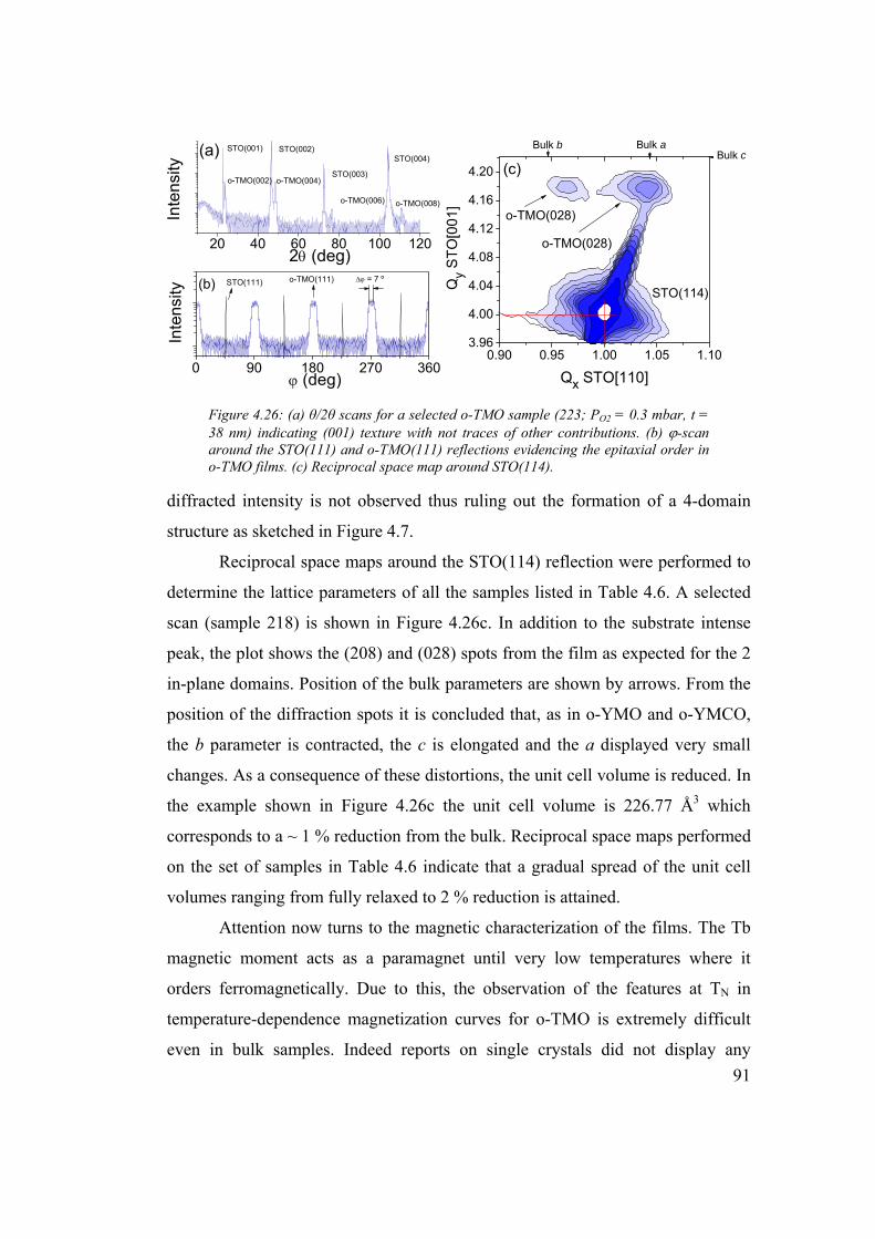
91
20 40 60 80 100 120
o-TMO(008)o-TMO(006)
o-TMO(004)
STO(004)
STO(003)
STO(002)
Inte
nsity
2θ (deg)
STO(001)
o-TMO(002)
(a)
0.90 0.95 1.00 1.05 1.103.96
4.00
4.04
4.08
4.12
4.16
4.20Bulk c
o-TMO(028)
Qx STO[110]
Qy
STO
[001
]
(c)
STO(114)
o-TMO(028)
Bulk b Bulk a
0 90 180 270 360
STO(111)
Inte
nsity
ϕ (deg)
o-TMO(111) (b) Δϕ = 7 º
Figure 4.26: (a) θ/2θ scans for a selected o-TMO sample (223; PO2 = 0.3 mbar, t = 38 nm) indicating (001) texture with not traces of other contributions. (b) ϕ-scan around the STO(111) and o-TMO(111) reflections evidencing the epitaxial order in o-TMO films. (c) Reciprocal space map around STO(114).
diffracted intensity is not observed thus ruling out the formation of a 4-domain
structure as sketched in Figure 4.7.
Reciprocal space maps around the STO(114) reflection were performed to
determine the lattice parameters of all the samples listed in Table 4.6. A selected
scan (sample 218) is shown in Figure 4.26c. In addition to the substrate intense
peak, the plot shows the (208) and (028) spots from the film as expected for the 2
in-plane domains. Position of the bulk parameters are shown by arrows. From the
position of the diffraction spots it is concluded that, as in o-YMO and o-YMCO,
the b parameter is contracted, the c is elongated and the a displayed very small
changes. As a consequence of these distortions, the unit cell volume is reduced. In
the example shown in Figure 4.26c the unit cell volume is 226.77 Å3 which
corresponds to a ~ 1 % reduction from the bulk. Reciprocal space maps performed
on the set of samples in Table 4.6 indicate that a gradual spread of the unit cell
volumes ranging from fully relaxed to 2 % reduction is attained.
Attention now turns to the magnetic characterization of the films. The Tb
magnetic moment acts as a paramagnet until very low temperatures where it
orders ferromagnetically. Due to this, the observation of the features at TN in
temperature-dependence magnetization curves for o-TMO is extremely difficult
even in bulk samples. Indeed reports on single crystals did not display any

92
0 50 100 150 200 250 3000
1
2
3
4
0 10 20 30 402
3
4
5
10 kOe 15 kOe 20 kOe Curie-Weiss
1/χ
(kO
e/ e
mu/
g)
Temperature (K)
FC
T (K)
m (1
0-5 e
mu)
ZFC
TC(Tb)
500 Oe
Figure 4.27: 1/χ measured at different magnetic fields in the paramagnetic region for a selected o-TMO sample (408; PO2 = 0.3 mbar, t = 140 nm). Inset: zoom of the low temperature region of a ZFC-FC curve showing TN(Tb) (signalled by vertical arrow) and the thermal irreversibility up to TN(Mn) ~ 40 K
remarkable feature at TN-Mn ~ 40 K [Mor07] and the 1/χ(T) displayed a linear
behaviour down to the ferromagnetic ordering of the Tb atoms.
Due to paramagnetic Tb contribution the total magnetic moment in the
high-temperature regime is:
BMnTbeff μμμμ 7.1022 ≈+= Eq. 4.1
where μTb and μMn are the effective paramagnetic moments of the Tb3+ (9.5
μB) and Mn3+ (4.9 μB) ions respectively. Since μTb ~ 2 · μMn, the total
susceptibility will be dominated by the Tb contribution. The susceptibility from
the Mn atoms can be estimated as the difference between the measured χ(T) and
the χTb(T) taken as:
TTCTb
Tb
0431.03
3 ≈=+
+χ emu/g/Oe · K Eq. 4.2
At the ordering temperature of the Mn sub-lattice, the total moment will
still increase due to the Tb paramagnetism although the Mn contribution is
expected to decrease. Data in Figure 4.27 displaying the χ-1(T) dependence of a
93
thick sample (408; PO2 = 0.3mbar, t = 140 nm) support this expectation. Magnetic
field is applied in-plane of the sample. The effective magnetic moment is
extracted from the fit of a Curie-Weiss law (solid line in Figure 4.27). It indicates
μeff ~ 12 μB and θp = 0 K. In agreement with measurements on single crystals
[Mor07], θp is close to zero. Due to the overlapped Tb contribution, the nature
(ferromagnetic or antiferromagnetic) of the Mn-O-Mn interactions cannot be
disclosed from the χ-1(T) curve. On the other hand, the obtained effective
magnetic moment is larger (but within the reasonable bounds for such
measurements in thin film) than the expected one (Eq. 4.1). The ordering of Tb
atoms observed in neutron diffraction [Kaj04] and magnetometry experiments
[Mor07] at TC(Tb) = 7 K is also observed as shown in the inset of Figure 4.27.
Furthermore, in close similarity to the o-YMO and o-YMCO films, the inset
reveals ZFC-FC thermal hysteresis for the o-TMO film indicating the presence of
net magnetic moment in the films. Note that the ZFC-FC splitting persists well
above the Tb3+ ions ordering temperature and is visible up to TN(Mn) ~ 40 K.
Therefore, it must be attributed to the Mn sub-lattice. This net magnetic moment
has been investigated in the o-TMO thin films first by magnetization loops and,
secondly, by ZFC-FC curves.
Magnetization loops of two o-TMO samples displaying different unit cell
distortion were measured and are showed in Figure 4.28 (panels a and b).
Attention is first focussed on the two magnetization loops recorded at T = 5 K <
TC(Tb) shown as solid symbols in each panel. Both loops exhibit a kink at
H ~ 2.5 T (signalled by arrows in the plot) that resembles the measurements on
single crystals performed by Kimura et al. on TbMnO3 where the kinks were
attributed to abrupt flops of Tb atoms [Kim03]. These kinks, attributed to the
ordered Tb atoms, vanished if magnetization loops were recorded at higher
temperatures [Kim03]. Effectively, loops at 15 K in Figure 4.28 support this
expectation: the kinks disappear, independently of the unit cell distortion, because
they are originated from Tb atoms. However, ferromagnetism is evidenced by the
broadening of the central part of the loop (displaying finite spontaneous
magnetization and coercitive field) also at 15 K which must be attributed to the
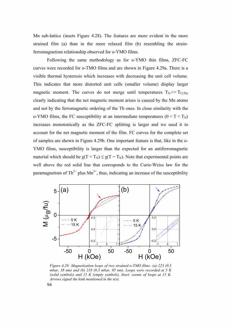
94
-50 0 50
-5
0
5
5 K 15 KM
(μB
/fu)
H (kOe)
(a)
-50 0 50
(b)
5 K 15 K
H (kOe)
-1 0 1-0.2
0.0
0.2
-1 0 1-0.2
0.0
0.2
Figure 4.28: Magnetization loops of two strained o-TMO films: (a) 223 (0.3 mbar, 38 nm) and (b) 218 (0.3 mbar, 95 nm). Loops were recorded at 5 K (solid symbols) and 15 K (empty symbols). Inset: zooms of loops at 15 K. Arrows signal the kink mentioned in the text.
Mn sub-lattice (insets Figure 4.28). The features are more evident in the more
strained film (a) than in the more relaxed film (b) resembling the strain-
ferromagnetism relationship observed for o-YMO films.
Following the same methodology as for o-YMO thin films, ZFC-FC
curves were recorded for o-TMO films and are shown in Figure 4.29a. There is a
visible thermal hysteresis which increases with decreasing the unit cell volume.
This indicates that more distorted unit cells (smaller volume) display larger
magnetic moment. The curves do not merge until temperatures TN >> TC(Tb)
clearly indicating that the net magnetic moment arises is caused by the Mn atoms
and not by the ferromagnetic ordering of the Tb ones. In close similarity with the
o-YMO films, the FC susceptibility at an intermediate temperatures (0 < T < TN)
increases monotonically as the ZFC-FC splitting is larger and we used it to
account for the net magnetic moment of the film. FC curves for the complete set
of samples are shown in Figure 4.29b. One important feature is that, like in the o-
YMO films, susceptibility is larger than the expected for an antiferromagnetic
material which should be χ(T < TN) ≤ χ(T = TN). Note that experimental points are
well above the red solid line that corresponds to the Curie-Weiss law for the
paramagnetism of Tb3+ plus Mn3+, thus, indicating an increase of the susceptibility

95
0 25 50 75 1000
5
10
(c)
V = 227.10 Å3
Temperature (K)
Vbulk = 229.04 Å3
0
5
10
(b)
V = 225.74 Å3 χ
25 K
(em
u/g/
kO
e)0
5
10 V = 224.84 Å3
(a)TN = 44 K
0 25 50 75 100
5
10
Vbulk = 229.04 Å3
(d)
224.84 Å3
225.74 Å3
226.97 Å3
226.77 Å3
227.10 Å3
228.39 Å3
228.82 Å3
χ (e
mu/
g /k
Oe)
Temperature (K)
Figure 4.29: ZFC-FC curves for 3 representative samples are shown in panels (a), (b), and (c). FC curves for the complete set of samples is presented in (b). The solid line represents the Curie-Weiss law for (Tb+Mn) paramagnetism.
as the unit cell distortion increases. In antiferromagnetic materials, a magnetic
field applied perpendicular to the antiferromagnetic axis induces a canting of the
spins which is larger if the susceptibility is larger. On the grounds of models for
the ferroelectricity obtained from the magnetic order (see Section 2.2.2), the
predicted atomic displacements and thus the electrical polarization depend on the
relative angle between neighbouring spins. Indeed, the dielectric properties are
expected to be modified by larger field-induced canting of the spins.
Of the highest relevance is that χ(T = 25K) plotted against the unit cell
volume clearly indicates that the magnetic response is determined by the unit cell
distortion (Figure 4.30). The more distorted unit cells, the more ferromagnetism.
To compare simultaneously o-YMO, o-YMCO, and o-TMO thin films,
paramagnetism from the Tb ions at 25 K has been removed using Eq. 4.2.
It is now discussed the physical picture for the ferromagnetism observed in
o-TMO films. The bulk magnetic structure of o-TMO is a spin spiral with the Mn
magnetic moments periodically tilted respect to the basal plane. The marked
similarities shown in Figure 4.30 between o-YMO and o-TMO correlations of
magnetic properties with epitaxial strain suggest that the magnetic structures in
both thin films are similar. This similarity may be explained as the trends in the
lattice parameters (b contraction and c elongation) indicate that Mn-O-Mn
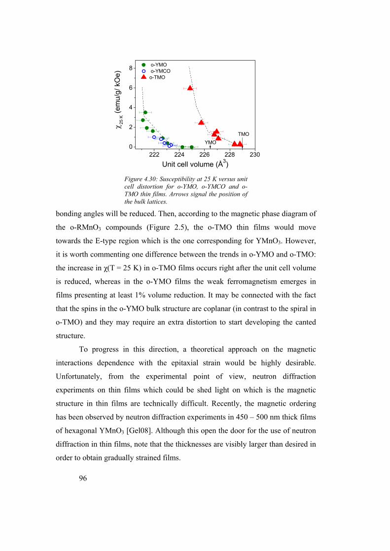
96
222 224 226 228 2300
2
4
6
8
TMO
o-YMO o-YMCOo-TMO
χ 25 K
(em
u/g/
kO
e)
Unit cell volume (Å3)
YMO
Figure 4.30: Susceptibility at 25 K versus unit cell distortion for o-YMO, o-YMCO and o-TMO thin films. Arrows signal the position of the bulk lattices.
bonding angles will be reduced. Then, according to the magnetic phase diagram of
the o-RMnO3 compounds (Figure 2.5), the o-TMO thin films would move
towards the E-type region which is the one corresponding for YMnO3. However,
it is worth commenting one difference between the trends in o-YMO and o-TMO:
the increase in χ(T = 25 K) in o-TMO films occurs right after the unit cell volume
is reduced, whereas in the o-YMO films the weak ferromagnetism emerges in
films presenting at least 1% volume reduction. It may be connected with the fact
that the spins in the o-YMO bulk structure are coplanar (in contrast to the spiral in
o-TMO) and they may require an extra distortion to start developing the canted
structure.
To progress in this direction, a theoretical approach on the magnetic
interactions dependence with the epitaxial strain would be highly desirable.
Unfortunately, from the experimental point of view, neutron diffraction
experiments on thin films which could be shed light on which is the magnetic
structure in thin films are technically difficult. Recently, the magnetic ordering
has been observed by neutron diffraction experiments in 450 – 500 nm thick films
of hexagonal YMnO3 [Gel08]. Although this open the door for the use of neutron
diffraction in thin films, note that the thicknesses are visibly larger than desired in
order to obtain gradually strained films.

97
0.95 1.00 1.05
4.0
4.1
4.2
Virgin, 30 nm
Qx[110]STO
Qy[
001]
STO
0.95 1.00 1.05
Anneal I, 30 nm
Qx[110]STO0.95 1.00 1.05
Anneal II, 30 nm
Qx[110]STO
YMO(028) (YMO(208)
STO(114)
Figure 4.31: Reciprocal space maps around the STO(114) reflection for a virgin sample and after two subsequent annealings. The top-left circle corresponds to the bulk position of the (028) reflection. Arrows connect the bulk position with the experimental location of the spot. It is clearly reduced after the second annealing.
4.6 Annealings of an orthorhombic YMnO3 sample
In order to obtain thin films with different lattice parameters, some
strategies have been used through the present thesis: modification of the
deposition conditions (PO2 pressure), thickness, and partial cationic substitution.
Post annealing of the thin films is an alternative path to modify the unit cell
parameters. Since the modifications in the unit cell topology can occur also via
changes in the oxygen content, annealings performed with or without an O2
atmosphere and/or at different temperatures allows controlling the oxygen
vacancies and getting insight of their relevance.
In order to investigate this issue, two subsequent annealings were
performed to an o-YMO sample (210). The annealing protocols were the
following: the first one consisted in 12 hours at 800 ºC on air; the second
consisted in 2 hours at 700 ºC on a 0.1 mbar Ar atmosphere. The lattice
parameters have been determined by reciprocal space maps after each annealing
and are shown in Figure 4.31. The bulk positions for the (028) diffraction spots
correspond to the top left corner of the plots and are signalled by a circle. An
arrow has been drawn as guide for the eye to evaluate the displacement of the
spots. FC susceptibility curves (H// = 500 Oe) were measured subsequently and
are shown in Figure 4.32a.
The χ(25 K) and the lattice parameters after each annealing are summarized

98
222 224 2260
2
4
0 50 100
2
4
Virgin Anneal #1 Anneal #2
(b)
χ (e
mu/
g/kO
e)
T (K)
(a)
H// = 500 Oe
Second annealing
Virgin sample
YMOYMCO
χ 25 K
(em
u/g/
kOe)
Unit cell volume (Å3)
YMO bulk
First annealing
Figure 4.32: (a) FC susceptibility curves (H//=500 Oe) for the virgin sample (0.1 mbar and 35 nm thick) and after two subsequent annealings. (b) shows the dependence of the magnetization at 25 K with the unit cell distortion for the annealed samples in the context of Figure 4.30.
in the Table 4.7. Experimental points are represented in Figure 4.32b.
χ25
(emu/g /kOe)
a (Å)
± 0.01 Å
b (Å)
± 0.01 Å
c (Å)
± 0.01 Å
Virgin (210) 3.71 5.257 5.673 7.419
12 h / air / 800 ºC 3.20 5.264 5.675 7.406
2 h / Ar / 700 ºC 1.08 5.259 5.728 7.400 Table 4.7: Susceptibility at 25 K and lattice parameters before and after the annealings described.
During the first annealing (in air), the out-of-plane parameter decreased
leading to a small contraction of the unit cell volume. Note that the changes of the
in-plane parameter are much smaller than the out-of-plane parameter. This could
be explained by the incorporation of oxygen in the o-YMO structure. The
magnetization decreases very slightly as expected according the the χ ↔ strain
correlation shown in Figure 4.32b. It is worth mentioning that there is observed a
more pronounced antiferromagnetic-like downturn of the magnetization on this
annealed sample. A diminution of oxygen vacancies would help reducing the
presence of eventual Mn4+ thus reinforcing the antiferromagnetic interactions. In
the second annealing (in Ar), the conditions were especially appropriate to induce
the creation of oxygen in the lattice. It caused a notable augment of the unit cell
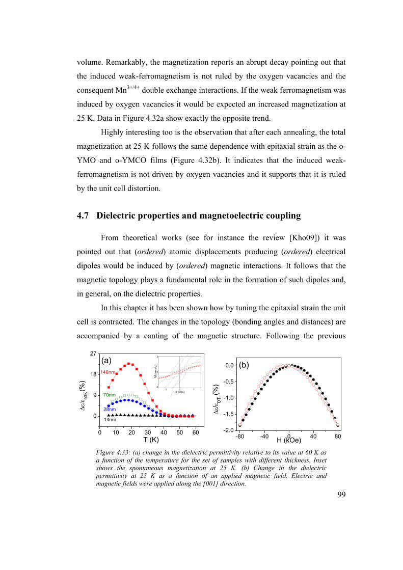
99
-1 0 1-2
0
2
0 10 20 30 40 50 60
0
9
18
27
T (K)
14nm
28nm
70nm
140nm
Δε/ε
60Κ(%
)
(a)
M (e
mu/
g)
H (kOe)
-80 -40 0 40 80-2.0
-1.5
-1.0
-0.5
0.0 (b)
Δε/ε
0T (%
)
H (kOe)
Figure 4.33: (a) change in the dielectric permittivity relative to its value at 60 K as a function of the temperature for the set of samples with different thickness. Inset shows the spontaneous magnetization at 25 K. (b) Change in the dielectric permittivity at 25 K as a function of an applied magnetic field. Electric and magnetic fields were applied along the [001] direction.
volume. Remarkably, the magnetization reports an abrupt decay pointing out that
the induced weak-ferromagnetism is not ruled by the oxygen vacancies and the
consequent Mn3+/4+ double exchange interactions. If the weak ferromagnetism was
induced by oxygen vacancies it would be expected an increased magnetization at
25 K. Data in Figure 4.32a show exactly the opposite trend.
Highly interesting too is the observation that after each annealing, the total
magnetization at 25 K follows the same dependence with epitaxial strain as the o-
YMO and o-YMCO films (Figure 4.32b). It indicates that the induced weak-
ferromagnetism is not driven by oxygen vacancies and it supports that it is ruled
by the unit cell distortion.
4.7 Dielectric properties and magnetoelectric coupling
From theoretical works (see for instance the review [Kho09]) it was
pointed out that (ordered) atomic displacements producing (ordered) electrical
dipoles would be induced by (ordered) magnetic interactions. It follows that the
magnetic topology plays a fundamental role in the formation of such dipoles and,
in general, on the dielectric properties.
In this chapter it has been shown how by tuning the epitaxial strain the unit
cell is contracted. The changes in the topology (bonding angles and distances) are
accompanied by a canting of the magnetic structure. Following the previous

100
paragraph, it is expected that the dielectric properties are changed as well.
Although the dielectric characterization of the films is formally outside the
objectives of the present thesis, it constitutes the natural next step to progress in
the work presented in this thesis. Now will be summarized the results, firstly, on
the dielectric and, secondly, on the magnetodielectric characterizations. I. Fina is
acknowledged for the dielectric characterization. Data in this section is already
published in Ref. [Mar09b].
A series of films (namely 250 – 253 as listed in Table 4.1) with different
thickness were grown by PLD on as-received 0.5% Nb doped STO(001)
substrates. Structural data from these samples is contained in Figure 4.10a and its
magnetization loops are reflected in Figure 4.19b.
Figure 4.33a shows the dielectric permittivity temperature dependence of
four samples of different thickness and having different strain. At the onset of the
antiferromagnetic ordering an anomaly is observed whose amplitude decreases
gradually with the unit cell distortion. This anomaly reproduces the reported one
in bulk o-YMO by Lorenz et al. [Lor04] and later in thin films by us [Mar07].
Magnetization loops are presented in the inset indicating that ferromagnetism is
correlated with strain. Data indicates that epitaxial strain rules simultaneously the
magnetic and dielectric properties.
To investigate the magnetoelectric coupling, dielectric permittivity has
0 5000 10000 15000-0.20
-0.15
-0.10
-0.05
0.00
28 nm64 nm
(a)ε r(Η) −
εr(Η
=0)
M2 (emu2/g2)
137 nm
Figure 4.34: linear dependence of the relative dielectric permittivity as a function of M2 for three samples with different thickness. Plots are presented shifted by the εr at zero magnetic field.
101
been measured at a constant temperature (25 K) as a function of the magnetic
field. Magnetic and electric fields have been applied along the [001] direction.
Data in Figure 4.33b shows that permittivity can be changed up to 2 % by
applying magnetic fields thus indicating a coupling between the electrical and
magnetic properties. Plot of the dielectric permittivity against M2 (Figure 4.34)
reveals a linear dependence as expected (see Chapter 2).
The most important result is that the magnetoelectric coupling can be
tailored by epitaxial strain as evidenced by the different slopes in curves
corresponding to different thickness (that is, different strain). The presence of
ferroelectricity and its correlation with the epitaxial strain remains to be proved in
these films and constitutes the current work in progress.
4.8 Summary of this chapter
o-YMO films have been grown on STO(001) substrates. The films are
orthorhombic, (001)-oriented and epitaxial. There are two crystal domains, 90 º
in-plane rotated, with the [001] and [010] directions of the o-YMO film parallel to
the [110] STO direction. As a result of an anisotropic in-plane lattice mismatch,
the films are strained anisotropically being compressive in the b direction, tensile
in the c direction negligible in the a direction. Unit cell volume (Vc) is an
appropriate parameter to account for all these distortions. Due to them, in all
samples the unit cell volume is reduced. This contraction is found to present a
small dependence with PO2 pressure, but a marked dependence on the film
thickness, being larger in thinner films. The important point is that o-YMO films
presenting a gradually contracted unit cell volumes can be obtained by selecting
the deposition conditions (background pressure and thickness).
More relaxed films have shown purely antiferromagnetic behavior. A
weak-ferromagnetic component is induced as unit cell distortions increase. This
component is found to be intrinsic. Some possible spurious origins are discussed
and discarded. The magnetic response is highly anisotropic. It can be understood
as a ferromagnetic component superposed to the pristine antiferromagnetic

102
anisotropy. A canting of the spins (aligned along b in the bulk material)
perpendicular to the b direction is revealed as the most physically plausible
scenario. The average canting angle is shown to be around 1 º.
In order to investigate the effects of the Mn sub-lattice topology (angles
and distances) without using the deposition conditions as variable parameters,
partial cationic substitutions and similar o-RMnO3 have been investigated. 5%
Co-substituted Mn films and TbMnO3 films were grown on STO(001) substrates.
Remarkably, ferromagnetism is also present in these films and follows exactly the
same correlations with unit cell topology as in o-YMO films. Effects of the
presence of Co or Tb ions are observed and discussed. Therefore, the induced
ferromagnetism arises as a genuine property of the strained Mn magnetic sub-
lattice.
Finally, magnetoelectric behavior has been demonstrated for o-YMO
films. The dielectric permittivity and the magnetoelectric coupling have been
shown to depend on the lattice distortion. The results indicate that it is possible to
obtain simultaneous magnetoelectric and ferromagnetic films adjusting the unit
cell parameters. The observation of ferroelectricity and its correlation with the
epitaxial strain constitutes the current work in progress.

103
5. Hexagonal YMnO3: Integration in functional heterostructures for electric control of magnetization
This chapter is devoted to the growth of hexagonal YMnO3 (h-YMO)
films and its integration in heterostructures with top ferromagnetic permalloy (Py)
layer to explore the electric-field induced effects on the exchange bias between
the two materials. The grounds to initialize this investigation were that the
ferroelectric and antiferromagnetic domain walls are coupled in h-YMO [Fie04]
and, then, it was expected a priori that the exchange bias and, thus, the Py
magnetization could be tuned via poling the h-YMO layer. The development of
such experiment requires the growth of h-YMO on conductive bottom electrodes,
whereas Py will act as top electrode. In such sandwich-like structure it is
convenient that the out-of-plane texture of the h-YMO films contains the
maximum possible (or the total) projection of the ferroelectric axis [0001] in order
to switch the ferroelectric state using the bottom Pt and top Py electrodes. To this
purpose, (0001)-oriented h-YMO films are required.
This chapter is divided in two sections. Firstly is described the growth and
structural characterization of the Py/h-YMO/Pt/Substrate heterostructure. In the
second part the functional characterizations and the electric field effects are
covered. Both sections are briefly described next.
The first part departs from the growth of h-YMO directly on bare
substrates in order to investigate the role of different deposition parameters to
obtain c-oriented h-YMO. In a second step is shown the development of bottom Pt
104
electrodes. These are epitaxial and (111) out-of-plane oriented in order to supply
the proper in-plane symmetry for the coherent growth of the subsequent (0001)-
oriented h-YMO layer. In a third step, the h-YMO is grown on Pt electrodes.
Results on XRD, AFM and TEM characterizations are presented.
The second part of this chapter covers the Py/h-YMO/Pt heterostructures.
The exchange bias between the h-YMO and Py is investigated by means of
SQUID magnetometry and anisotropic magnetoresistance (AMR). The
dependencies of the exchange bias on the temperature and the magnetic field in
each set-up are discussed. Finally, it is shown that biasing with an electric field
induces changes in the exchange bias and, consequently, in the magnetization of
the top Py electrode, even achieving a reversal in the Py magnetization. Critical
assessment of distinct experimental conditions to investigate if the observed effect
could be also induced by the coexistence of Joule effect is presented. It is
concluded the existence of a genuine electric-field effect on the exchange bias.
5.1 Growth and structural characterization
5.1.1 h-YMO monolayers
This section describes the optimization of the deposition parameters in
order to obtain epitaxial h-YMO(0001) films. The choice of the substrates
according to the lattice mismatch is discussed first. Next, the structural
characterizations (by XRD and AFM) are presented aiming to determine the
optimal growth conditions.
Substrates presenting a three-fold symmetry at the surface are required for
a coherent growth of an upper (0001)-oriented h-YMO layer. Three substrates
were selected for growth as listed in Table 5.1. The out-of-plane orientation in
each case is presented in the second column. The corresponding in-plane
mismatch, calculated as f = 100 · (aSubstrate - dYMO) / dYMO, is presented at the right
column for each case. The atomic arrangements at the (0001) h-YMO surface and
for the substrates listed in Table 5.1 are shown in Figure 5.1. In the pictures,
aSubstrate distances are represented by green arrows.

105
a
bdYMO
YMn
O
[1230]h-YMO
(a)
h-YMnO3(0001)
a
b
ca
b
c
a
bc
a
bc
Al2O3(0001)
a
b
c a
b
c
Y:ZrO2(0001)
SrTiO3(111)(b)
(c) (d)
Figure 5.1: Sketch of the atomic arrangement at (a) the (0001) h-YMO surface (Y, Mn, and O atoms are denoted), (b) SrTiO3(111), (c) Al2O3(0001), and (d) Y-ZrO2(111). Film’s Oxygen atoms are plotted always as blue spheres. In panels (b), (c) and (d) cations are coloured as: (b) yellow Sr, orange Ti, (c) red Al, and (d) yellow Zr.
Data for the bulk YMnO3 unit cell has been taken from Ref. [Ake00]:
a = b = 6.14 Å, c = 11.41 Å in the P63cm setting. The distance dYMO corresponds
to the Mn-Mn distance in the [1230] direction (3.60 Å) as shown in Figure 5.1a.
For the Al2O3 substrate, the in-plane lattice parameter in the R3c setting is taken
from Ref. [Kon08]. For the SrTiO3(111) and Y:ZrO2(111) substrates, the in-plane
distance used for the mismatch calculation is a·√2/2 from Refs. [Mey81] and
[Lam00], respectively. From data in Table 5.1, it turns out that this selection of
substrates allows studying the growth of h-YMO(0001) films under compressive,
tensile and zero strain, respectively.
Substrate Out-of-plane
orientation Mismatch, f (%)
SrTiO3 (STO) (111) -0.28
Al2O3 (ALO) (0001) +0.26
Y:ZrO2 (YSZ) (111) +0.02 Table 5.1: Lattice mismatch of h-YMO(0001) on several substrates. Data is calculated from data in Refs. [Mey81], [Lam00] and [Kon08].
Thin films of h-YMO were deposited by PLD on the mentioned substrates.

106
20 40 60 80 100
(d)
YMO(006)
YMO(004)
YMO(002)
YSZ(111)
oYMO(40
4)
STO(222)
oYMO(20
2)
STO(111)
2θ (deg)
ALO(00
06)
Inte
nsity
(arb
.uni
ts)
(c)
(b)YMO(00
8)
YSZ(222)
Figure 5.2: θ/2θ scans corresponding to 90 nm thick h-YMO samples grown at 800 ºC and 0.2 mbar on (a) YSZ(111), (b) STO(111), and (c) ALO(0001) substrates..
As-received substrates with miscut angle nominally below 0.2 º were used. In an
initial exploration, 100 nm thick films were deposited in the range of 750 ºC -
825 ºC and 0.02 mbar - 0.3 mbar of oxygen. The films were subsequently
analyzed by XRD and in Figure 5.2 are presented θ/2θ scans of selected samples
(800 ºC, 0.2 mbar) which are representative of the results on each substrate. The
qualitative observations within the range of conditions explored were:
First, on YSZ(111) substrates, epitaxial hexagonal (0001)-oriented films
were obtained with no other traces of other phases and/or reflections. This results
are in agreement with the reports by other authors [Dho04, Gel09] on h-YMO
films grown on YSZ(111).
Second, on STO(111) substrates, epitaxial (101)-oriented orthorhombic
films were obtained. The results on films grown on STO(111) and the reason why
the orthorhombic phase is stabilized are thoroughly discussed in Appendix D.
Third, no diffraction peaks from any crystalline material were found on
ALO(0001). The absence of textured material on this substrate contrasts with the
reported hexagonal epitaxial films reported by Dho et al. [Dho04]. It must be
noted that Dho et al. films were grown in a range of pressures (< 0.01 mbar O2)
clearly out of our explored region. The growth rate (modified by the PO2 pressure)
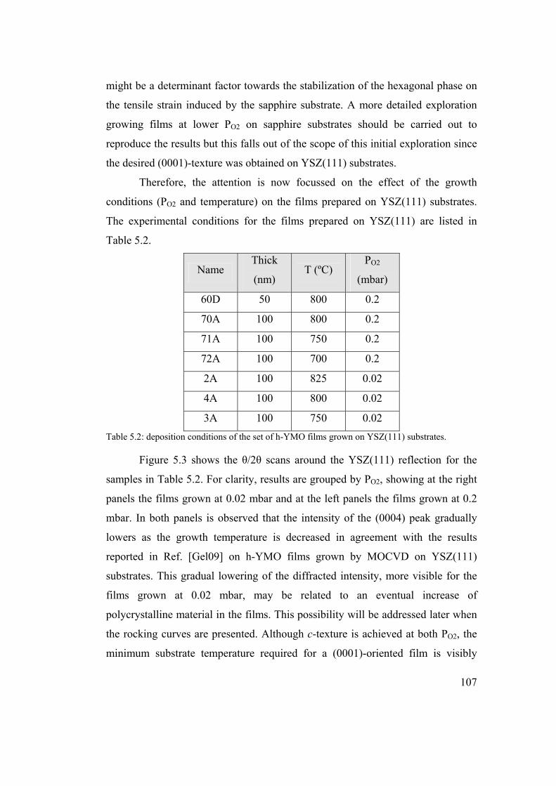
107
might be a determinant factor towards the stabilization of the hexagonal phase on
the tensile strain induced by the sapphire substrate. A more detailed exploration
growing films at lower PO2 on sapphire substrates should be carried out to
reproduce the results but this falls out of the scope of this initial exploration since
the desired (0001)-texture was obtained on YSZ(111) substrates.
Therefore, the attention is now focussed on the effect of the growth
conditions (PO2 and temperature) on the films prepared on YSZ(111) substrates.
The experimental conditions for the films prepared on YSZ(111) are listed in
Table 5.2.
Name Thick
(nm) T (ºC)
PO2
(mbar)
60D 50 800 0.2
70A 100 800 0.2
71A 100 750 0.2
72A 100 700 0.2
2A 100 825 0.02
4A 100 800 0.02
3A 100 750 0.02 Table 5.2: deposition conditions of the set of h-YMO films grown on YSZ(111) substrates.
Figure 5.3 shows the θ/2θ scans around the YSZ(111) reflection for the
samples in Table 5.2. For clarity, results are grouped by PO2, showing at the right
panels the films grown at 0.02 mbar and at the left panels the films grown at 0.2
mbar. In both panels is observed that the intensity of the (0004) peak gradually
lowers as the growth temperature is decreased in agreement with the results
reported in Ref. [Gel09] on h-YMO films grown by MOCVD on YSZ(111)
substrates. This gradual lowering of the diffracted intensity, more visible for the
films grown at 0.02 mbar, may be related to an eventual increase of
polycrystalline material in the films. This possibility will be addressed later when
the rocking curves are presented. Although c-texture is achieved at both PO2, the
minimum substrate temperature required for a (0001)-oriented film is visibly
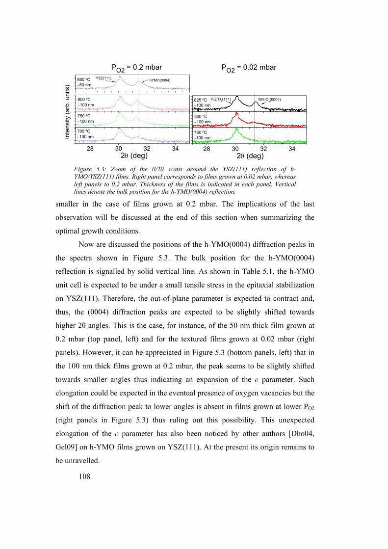
108
28 30 32 342θ (deg)
700 ºC∼100 nm
750 ºC∼100 nm
800 ºC∼100 nm
Inte
nsity
(arb
. uni
ts)
PO2 = 0.2 mbarYSZ(111)800 ºC
∼50 nmhYMO(0004)
28 30 32 34
750 ºC∼100 nm
2θ (deg)
800 ºC∼100 nm
PO2 = 0.02 mbar
Y-ZrO2(111) YMnO
3(0004)825 ºC
∼100 nm
Figure 5.3: Zoom of the θ/2θ scans around the YSZ(111) reflection of h-YMO/YSZ(111) films. Right panel corresponds to films grown at 0.02 mbar, whereas left panels to 0.2 mbar. Thickness of the films is indicated in each panel. Vertical lines denote the bulk position for the h-YMO(0004) reflection.
smaller in the case of films grown at 0.2 mbar. The implications of the last
observation will be discussed at the end of this section when summarizing the
optimal growth conditions.
Now are discussed the positions of the h-YMO(0004) diffraction peaks in
the spectra shown in Figure 5.3. The bulk position for the h-YMO(0004)
reflection is signalled by solid vertical line. As shown in Table 5.1, the h-YMO
unit cell is expected to be under a small tensile stress in the epitaxial stabilization
on YSZ(111). Therefore, the out-of-plane parameter is expected to contract and,
thus, the (0004) diffraction peaks are expected to be slightly shifted towards
higher 2θ angles. This is the case, for instance, of the 50 nm thick film grown at
0.2 mbar (top panel, left) and for the textured films grown at 0.02 mbar (right
panels). However, it can be appreciated in Figure 5.3 (bottom panels, left) that in
the 100 nm thick films grown at 0.2 mbar, the peak seems to be slightly shifted
towards smaller angles thus indicating an expansion of the c parameter. Such
elongation could be expected in the eventual presence of oxygen vacancies but the
shift of the diffraction peak to lower angles is absent in films grown at lower PO2
(right panels in Figure 5.3) thus ruling out this possibility. This unexpected
elongation of the c parameter has also been noticed by other authors [Dho04,
Gel09] on h-YMO films grown on YSZ(111). At the present its origin remains to
be unravelled.

109
-1.0 -0.5 0.0 0.5 1.00.00
0.25
0.50
0.75
1.00 100 nm 50 nm
Inte
nsity
(a.u
.)
Δω (deg)-1.0 -0.5 0.0 0.5 1.0
100 nm
Δω (deg)-1.0 -0.5 0.0 0.5 1.0
100 nm
Δω (deg)
YSZ(200)
YSZ(111)
h-YMO(1124)
h-YMO(1122)
h-YMO(1123)
h-YMO(2022)
h-YMO(1012)
YSZ(200)
YSZ(111)
h-YMO(1124)
h-YMO(1122)
h-YMO(1123)
h-YMO(2022)
h-YMO(1012)
800 ºC 750 ºC 700 ºC
800 ºC 750 ºC 700 ºC
(a) (b) (c)
(d) (e) (f)
Figure 5.4: rocking curves for films grown at PO2 = 0.2 mbar at (a) 800 ºC, (b) 750 ºC, and (c) 700 ºC. A 50 nm thick film grown at 800 ºC is also displayed in panel a. Panels (d-f) show the pole figures performed with a 2-dimensional detector for the 100 nm thick films grown at (d) 800 ºC, (e) 750 ºC, and (f) 700 ºC. Reflections from the substrate and the films are labelled only in panel (d).
Now is addressed the crystal quality of the films which has been monitored
via the full width at half maximum (FWHM) of rocking curves around the h-
YMO(0004) reflection. Data for the samples grown at 0.2 mbar are shown in
Figure 5.4 (panels a-c). FWHM of 100 nm thick films (solid symbols) is found to
remain constant at around 1 º, independent of the temperature. For films 50 nm
thick (empty symbols in panel a) the value is very similar. The FWHM for the
substrate’s YSZ(111) reflection is below 0.05 º.
The reported values for the FWHM of rocking curves in the literature are
visibly smaller than in our films: 0.06 º and ~ 0.15 º for references [Dho04] and
[Gel09], respectively for h-YMO films grown on YSZ(111) and with similar
thickness. As we mentioned before, there is the possibility that a significant
amount of polycrystalline is present in the films. This issue has been investigated
by XRD using a 2-dimensional detector. Data for asymmetrical reflections for the
100 nm films are shown in panels (d-f) for three different temperatures.
Reflections from the h-YMO films (only labelled in panel d) appear at the
expected positions for a (0001)-oriented h-YMO. It is observed a tiny
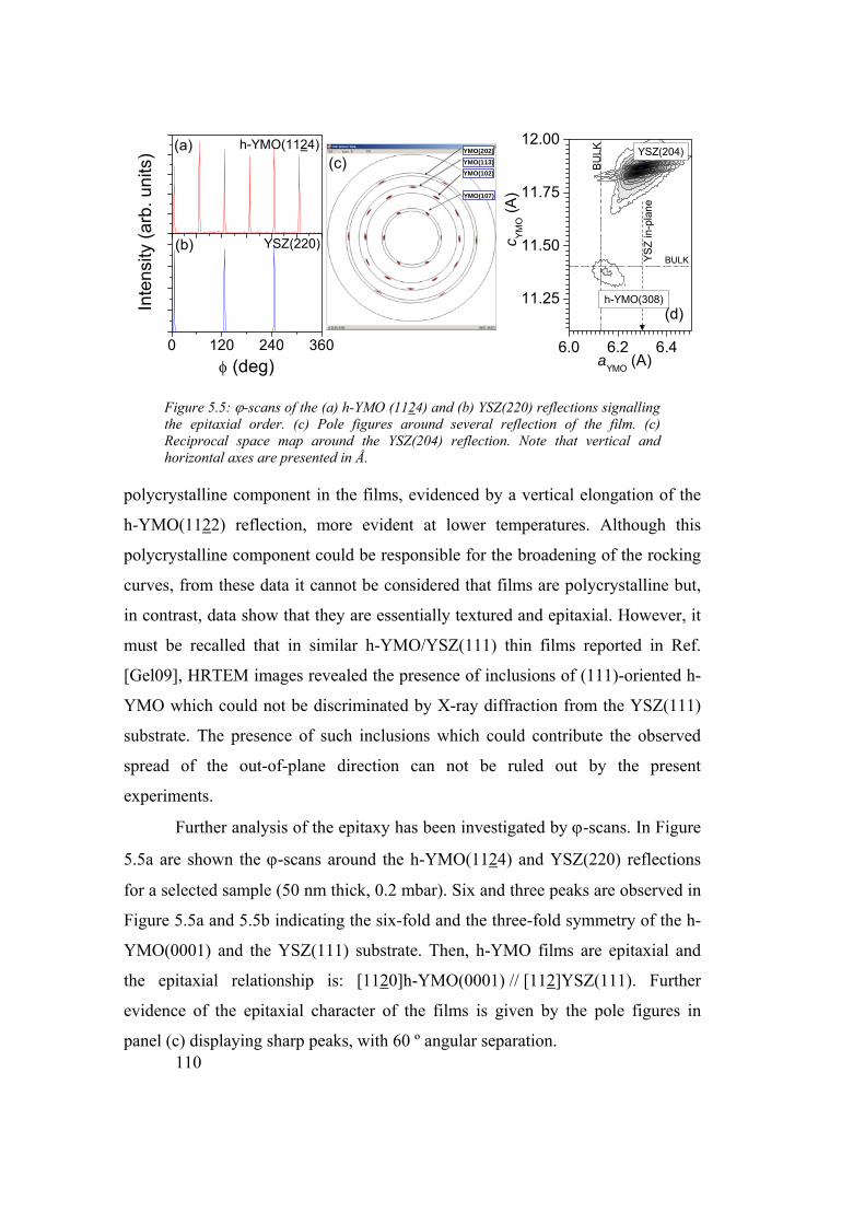
110
0 120 240 360
YSZ(220)
Inte
nsity
(arb
. uni
ts)
φ (deg)
(a)
(b)
h-YMO(1124)(c)
6.0 6.2 6.4
11.25
11.50
11.75
12.00YSZ(204)
c YM
O (A
)
aYMO (A)
YSZ
in-p
lane
BULK
BULK
h-YMO(308)(d)
YMO(202)YMO(113)YMO(102)
YMO(107)
Figure 5.5: ϕ-scans of the (a) h-YMO (1124) and (b) YSZ(220) reflections signalling the epitaxial order. (c) Pole figures around several reflection of the film. (c) Reciprocal space map around the YSZ(204) reflection. Note that vertical and horizontal axes are presented in Å.
polycrystalline component in the films, evidenced by a vertical elongation of the
h-YMO(1122) reflection, more evident at lower temperatures. Although this
polycrystalline component could be responsible for the broadening of the rocking
curves, from these data it cannot be considered that films are polycrystalline but,
in contrast, data show that they are essentially textured and epitaxial. However, it
must be recalled that in similar h-YMO/YSZ(111) thin films reported in Ref.
[Gel09], HRTEM images revealed the presence of inclusions of (111)-oriented h-
YMO which could not be discriminated by X-ray diffraction from the YSZ(111)
substrate. The presence of such inclusions which could contribute the observed
spread of the out-of-plane direction can not be ruled out by the present
experiments.
Further analysis of the epitaxy has been investigated by ϕ-scans. In Figure
5.5a are shown the ϕ-scans around the h-YMO(1124) and YSZ(220) reflections
for a selected sample (50 nm thick, 0.2 mbar). Six and three peaks are observed in
Figure 5.5a and 5.5b indicating the six-fold and the three-fold symmetry of the h-
YMO(0001) and the YSZ(111) substrate. Then, h-YMO films are epitaxial and
the epitaxial relationship is: [1120]h-YMO(0001) // [112]YSZ(111). Further
evidence of the epitaxial character of the films is given by the pole figures in
panel (c) displaying sharp peaks, with 60 º angular separation.
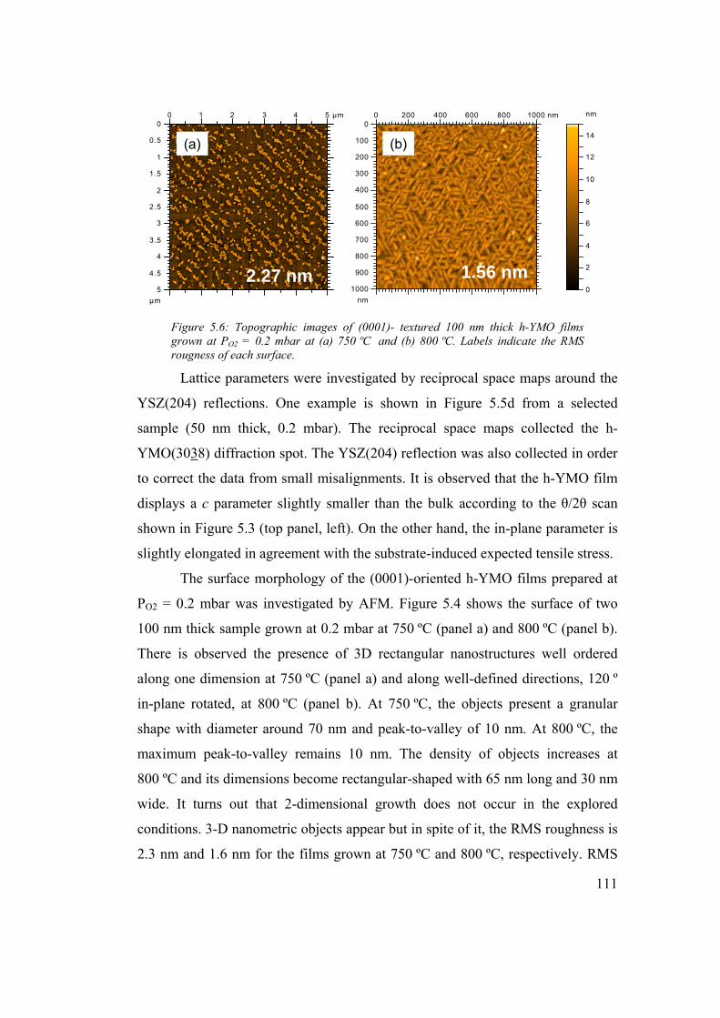
111
1.07 nm
nm
0
2
4
6
8
10
12
14
0 1 2 3 4 5 µm
µm
0
0.5
1
1.5
2
2.5
3
3.5
4
4.5
5
nm
0
2
4
6
8
10
12
14
0 200 400 600 800 1000 nm
nm
0
100
200
300
400
500
600
700
800
900
1000
1.56 nm
(a) (b)
2.27 nm
Figure 5.6: Topographic images of (0001)- textured 100 nm thick h-YMO films grown at PO2 = 0.2 mbar at (a) 750 ºC and (b) 800 ºC. Labels indicate the RMS rougness of each surface.
Lattice parameters were investigated by reciprocal space maps around the
YSZ(204) reflections. One example is shown in Figure 5.5d from a selected
sample (50 nm thick, 0.2 mbar). The reciprocal space maps collected the h-
YMO(3038) diffraction spot. The YSZ(204) reflection was also collected in order
to correct the data from small misalignments. It is observed that the h-YMO film
displays a c parameter slightly smaller than the bulk according to the θ/2θ scan
shown in Figure 5.3 (top panel, left). On the other hand, the in-plane parameter is
slightly elongated in agreement with the substrate-induced expected tensile stress.
The surface morphology of the (0001)-oriented h-YMO films prepared at
PO2 = 0.2 mbar was investigated by AFM. Figure 5.4 shows the surface of two
100 nm thick sample grown at 0.2 mbar at 750 ºC (panel a) and 800 ºC (panel b).
There is observed the presence of 3D rectangular nanostructures well ordered
along one dimension at 750 ºC (panel a) and along well-defined directions, 120 º
in-plane rotated, at 800 ºC (panel b). At 750 ºC, the objects present a granular
shape with diameter around 70 nm and peak-to-valley of 10 nm. At 800 ºC, the
maximum peak-to-valley remains 10 nm. The density of objects increases at
800 ºC and its dimensions become rectangular-shaped with 65 nm long and 30 nm
wide. It turns out that 2-dimensional growth does not occur in the explored
conditions. 3-D nanometric objects appear but in spite of it, the RMS roughness is
2.3 nm and 1.6 nm for the films grown at 750 ºC and 800 ºC, respectively. RMS

112
roughness in the films is slightly larger than the typically below 1 nm reported in
Ref. [Gel09] for 25 nm thick films grown by MOCVD and visibly larger than the
0.1 nm reported in Ref. [Dho04] for films grown by PLD at smaller PO2 < 0.01
mbar although in the reference it was not specified the thickness of the samples
displayed.
In summary, the moderately large RMS roughness and the broad rocking
curves indicate that the growth of the h-YMO films on YSZ(111) is far from the
optimal conditions. From this initial exploration of the growth conditions, it has
been concluded that, at constant PO2, the amount of material presenting the (0001)
texture increases as growth temperature increases. However, recall that the
ultimate objective of this thesis is to obtain h-YMO films, (0001)-oriented, on
platinum layers. Very recent work performed at ICMAB concluded that the
growth temperature of the h-YMO layer must be kept as low as possible to
prevent the degradation of the Pt layer [Bac09]. As a consequence, the optimal
growth temperature for the h-YMO film will be ruled by the stability of the
bottom Pt layer. Regarding PO2, the data in this section showed that, at constant
growth temperature, films grown at larger PO2 displayed more intense (0004) h-
YMO peaks. Therefore, the optimal PO2 growth conditions are chosen to be PO2 =
0.2 mbar which is the highest PO2 explored in this section. As a final remark, since
the objective of the thesis is to obtain epitaxial films on Pt bottom electrodes, no
further efforts to optimize the growth on YSZ(111) have been attempted.
5.1.2 Bottom Pt electrodes
This section describes the growth by dc sputtering of the bottom Pt
electrodes and the structural characterization. After a brief introduction, the θ/2θ
XRD characterization of Pt films on STO(111) and ALO(0001) is covered.
Finally, the AFM characterization of the Pt buffer layers grown on both substrates
is presented.
In the description of the state of the art in Chapter 2, it has been mentioned
that Pt (111)-oriented buffered substrates is the usual choice in the literature as a

113
20 40 60 80 100
(b) ALO(00012)
Pt(222)
Pt(222)
ALO(0006)
Pt(111)
2θ (deg)
Pt(111)
STO(222)STO(111)
Inte
nsity
(arb
. uni
ts)
(a)
35 40 45
2θ (deg)
35 40 45
2θ (deg)
Figure 5.7: θ/2θ scans of 14.4 nm thick Pt films grown at 500 ºC on (a) Al2O3(0001) and (b) SrTiO3(111) substrates. Inset: zoom showing the Laue fringes around the Pt(111) reflections.
bottom layer for obtaining c-textured h-YMO. Following the literature
background [Ast03, Duc03], STO(111) and ALO(0001) substrates were selected
for the growth of Pt (111)-oriented epitaxial films. Pt films were deposited by dc
sputtering during a 2 month stage at CNRS-ONERA (Toulouse, France). Prior to
all depositions, as-received substrates were heated at 800 ºC for 10 minutes and,
afterwards, cooled down to deposition temperature where Ar was introduced into
the chamber up to 5·10-3 mbar. Pt films with thickness in the 4 – 180 nm range
were grown at 500 ºC and at a growth rate of 1.8 nm/min. Samples 7.2 nm thick
were also grown at 400 ºC, 500 ºC and 600 ºC in order to investigate the
temperature effect on the Pt buffer layers that, in a following step, will be used as
substrates to grow the h-YMO films at temperatures in the 700 – 800 C range.
In Figure 5.7 are presented the θ/2θ scans corresponding to 14.4 nm thick
Pt layers grown at 500 ºC on STO(111) (panel a) and ALO(0001) (panel b). Scans
show only reflections from the Pt(111) texture on both substrates. These features
are present in all films in the thickness and temperature range explored.
Interestingly, clear Laue oscillations are observed and are a signature of high
quality films with smooth interfaces. These oscillations are visible in Pt films of
thickness below 14.4 nm.

114
30 35 40 45 50
180 nm
90 nm
45 nm
14.4 nm
7.2 nm
2θ (deg)
3.6 nmInte
nsity
(arb
. uni
ts) Pt(111) ALO(0006)
30 35 40 45 50
2θ (deg)
180 nm
90 nm
45 nm
14.4 nm
7.2 nm
3.6 nm
Pt(111) STO(111)(a) (b)
Figure 5.8: Zoom of θ/2θ scans around Pt(111) reflection for films of different thickness grown at 500 ºC on (a) ALO(0001) and (b) STO(111) substrates. Arrows signal the position of the Pt(111) peaks.
0 50 100 150 2002.26
2.27
2.28
2.29 Pt(111)/STO(111)Pt(111)/ALO(0001)
d Pt(1
11)(Å
)
Thickness (nm)
Bulk Pt(111)
Figure 5.9: Out-of-plane parameter of the Pt(111) films grown at 500 ºC versus thickness showing a gradual relaxation with thickness on STO(111) (solid circles) and on ALO(0001) (empty circles). Solid horizontal line signals the bulk Pt(111) interplanar distance from Ref. [Edw51].
The results on the XRD characterization for Pt films with different
thickness are now presented. Figure 5.8 show a zoom around the Pt(111)
reflection for films of different thickness (labelled in the figure) grown at 500 ºC
on both ALO(0001) (panel a) and STO(111) (panel b) substrates. In both panels, it
can be appreciated a small shift to the Pt(111) reflection with respect to the bulk
position (signalled by vertical solid line) which gradually fades away as thickness
increases. The bulk position for the Pt(111) reflection (2θ = 39.748 º) has been
calculated using Bragg’s law and the Pt lattice parameter from Ref. [Edw51] (aPt
= 3.924 Å at room temperature). This shift to lower angles indicates an expansion
of the out-of-plane parameter, dPt(111), on both substrates caused, as it will be

115
30 35 40 45 50
400 ºC
2θ (deg)
(a)
500 ºC
Inte
nsity
(arb
. uni
ts)
Pt(111) ALO(0006)
600 ºC
500 ºC
30 35 40 45 50
400 ºC
2θ (deg)
(b) 600 ºC
STO(111)Pt(111)
Figure 5.10: Zoom of θ/2θ scans around the 7.2 nm thick Pt(111) films grown at different temperatures on (a) ALO(0001) and on (b) STO(111) substrates. Vertical dashed line is a guide for the eye.
shown after the determination of the epitaxial relationships, by the in-plane tensile
stress induced by the substrate. As the thickness of the Pt layer increases, the film
progressively relaxes and the mentioned shift gradually vanishes. The out-of-
plane parameters obtained from Bragg’s law are summarized in Figure 5.9. Data
show the mentioned increasing relaxation of the Pt layer with increasing thickness
on both STO(111) and ALO(0001) substrates.
Now is presented the XRD characterization of Pt films grown at different
temperatures. Figure 5.10 show the XRD θ/2θ scan for 7.2 nm thick Pt films
grown at 400 ºC, 500 ºC and 600 ºC on ALO(0001) (panel a) and on STO(111)
(panel b) substrates. Scans show that the Laue fringes signalling smooth interface
and high quality film are not modified by the growth temperature on both
substrates. Neither the angular position of the Pt(111) peak is changed in films
grown at different temperatures. Therefore, it is concluded from the XRD
characterization that the quality of the Pt buffer layers and the epitaxial strain does
not depend on the substrate growth temperature in the explored 400 – 600 ºC
range.
Rocking curves around the Pt(111) reflection for films grown at 500 ºC on
ALO(0001) substrates were recorded. Figure 5.11 (panel a) shows the dependence
of the FWHM with the film thickness. Raw data for a selected Pt/ALO(0001)
sample (500 ºC, 45 nm thick) is shown in the inset. FWHM is found to increase as

116
0 100 2000.2
0.3
0.4
0.5
FHW
M (º
)
Film thickness (nm)
20.0 20.4
Inte
nsity
(a.u
.)
ω (º)
(a) (b)
Pt(200)
ALO(1123)
Pt(111)
ALO(2022)
ALO(1014)
ALO(0112)
Figure 5.11: (a) FWHM of rocking curves around the Pt(111) reflection for films with different thickness grown at 500 ºC on ALO(0001) substrates. Solid line is guide for the eye. Inset: raw data (and fitting as solid line) for a 7.2 nm thick film. (b) XRD frame obtained with 2-dimensional area detector for the 45 nm thick Pt film grown at 500 ºC on ALO(0001).
film thickness increases. Rocking curves appear to be quite broad but comparable
to values reported in the literature [Far93] for Pt/ALO films. As in the case of h-
YMO/YSZ(111) films, it has been investigated if the broadness of the rocking
curves could be caused by the presence of some amount of polycrystalline
material. A XRD frame obtained with the 2-dimensional area detector is shown in
Figure 5.11b for the 45 nm thick Pt film. All the observed peaks can be indexed
assuming Pt(111) textured material on ALO(0001). The absence of vertical
elongations of the diffraction peaks evidences the absence of polycrystalline Pt
within the experimental resolution. Rocking curves in the out-of-plane direction
of Pt/STO(111) films were not recorded because the Pt reflections are always
closer to STO(111) reflections and data for the Pt(111) film is masked by the
contribution of the STO(111) substrate.
Attention is now focussed on the Laue oscillations observed around the
Pt(111) reflections in films with thickness below 14.4 nm. Figure 5.6b shows a
zoom around Pt(111) peak in reciprocal space units for a Pt/ALO(0001) (panel a)
and for a P/STO(111) (panel b) film. Laue oscillations are found to follow the
expected I(q)~sin2(N·πq)/sin2(πq) dependence in both cases. N is the number of
unit cells in the direction perpendicular to the surface of the film and q are the
reciprocal space coordinates (horizontal axis). By fitting (shown as red line in the
plot) the previous function, film’s thickness can be derived. It turns out that, for
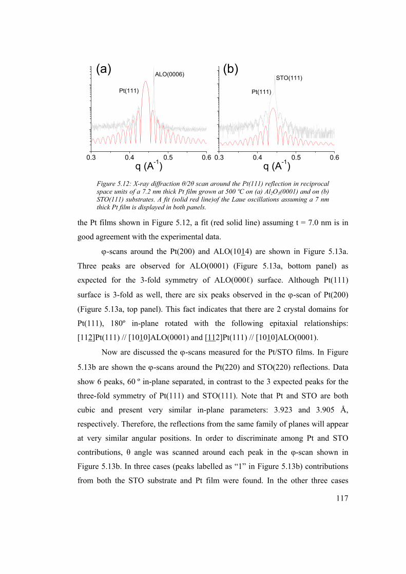
117
0.3 0.4 0.5 0.6q (A-1)
Pt(111)
ALO(0006)
0.3 0.4 0.5 0.6
Pt(111)
q (A-1)
STO(111)(a) (b)
Figure 5.12: X-ray diffraction θ/2θ scan around the Pt(111) reflection in reciprocal space units of a 7.2 nm thick Pt film grown at 500 ºC on (a) Al2O3(0001) and on (b) STO(111) substrates. A fit (solid red line)of the Laue oscillations assuming a 7 nm thick Pt film is displayed in both panels.
the Pt films shown in Figure 5.12, a fit (red solid line) assuming t = 7.0 nm is in
good agreement with the experimental data.
ϕ-scans around the Pt(200) and ALO(1014) are shown in Figure 5.13a.
Three peaks are observed for ALO(0001) (Figure 5.13a, bottom panel) as
expected for the 3-fold symmetry of ALO(000ℓ) surface. Although Pt(111)
surface is 3-fold as well, there are six peaks observed in the ϕ-scan of Pt(200)
(Figure 5.13a, top panel). This fact indicates that there are 2 crystal domains for
Pt(111), 180º in-plane rotated with the following epitaxial relationships:
[112]Pt(111) // [1010]ALO(0001) and [112]Pt(111) // [1010]ALO(0001).
Now are discussed the ϕ-scans measured for the Pt/STO films. In Figure
5.13b are shown the ϕ-scans around the Pt(220) and STO(220) reflections. Data
show 6 peaks, 60 º in-plane separated, in contrast to the 3 expected peaks for the
three-fold symmetry of Pt(111) and STO(111). Note that Pt and STO are both
cubic and present very similar in-plane parameters: 3.923 and 3.905 Å,
respectively. Therefore, the reflections from the same family of planes will appear
at very similar angular positions. In order to discriminate among Pt and STO
contributions, θ angle was scanned around each peak in the φ-scan shown in
Figure 5.13b. In three cases (peaks labelled as “1” in Figure 5.13b) contributions
from both the STO substrate and Pt film were found. In the other three cases

118
(a)
Inte
nsity
(arb
. uni
ts)
0 120 240 360
(b)
φ (deg)
0 120 240 360
φ (deg)67.2 67.7 68.2
(c)
2
222
1
11
STO(220)
2θ (deg)
Pt(220)
1
Figure 5.13: XRD φ-scans corresponding to (a) Pt/ALO and (b) Pt/STO films. Panel (c) details the presence of either both STO and Pt or only Pt contributions in the Pt(220) φ-scan in bottom plot in (b).
(labelled as “2” in Figure 5.13b), only Pt contributions were found. It turns out
that, for the Pt(220) reflection, there are six Pt peaks, 60 º in-plane spaced.
Therefore, there are two Pt crystal domains on the STO substrate, 180 º in-plane
rotated. The epitaxial relationship for the Pt domains are: [112]Pt(111) //
[112]STO(111) and [112]Pt(111) // [112]STO(111).
The epitaxial relationships obtained from the φ-scans shown in Figure 5.13
are sketched in Figure 5.14. From the epitaxial relationship for the Pt/ALO(0001)
films (panel a), it is found that the distance L = 3/2·√2·aPt (~ 8.32 Å) is
accommodated on √3·aALO (~ 8.22 Å). In the case of Pt/STO(111) films, the
√2/2·aPt (2.77 Å) must fit on √2/2·aSTO (2.76 Å). From the numerical values, it
turns out that the lattice mismatches, calculated as 100·(asubstrate – afilm) / afilm, are -
1.0% and -0.4% on ALO(0001) and STO(111), respectively. Therefore, Pt films
on both ALO(0001) and STO(111) substrates are under in-plane compressive
stress. As a consequence, an expansion of the out-of-plane parameter, dPt(111),
should be expected in agreement with data in Figure 5.9.

119
Pt(111) //Al2O3(0001)[112]Pt//[1010]Al2O3
Pt(111) //SrTiO3(111)[112]Pt//[112]SrTiO3
(a)
(b)
[1010]ALO
[110]Pt
[112]Pt
[110]STO
L
Pt(111) //Al2O3(0001)[112]Pt//[1010]Al2O3
Pt(111) //SrTiO3(111)[112]Pt//[112]SrTiO3
(a)
(b)
[1010]ALO
[110]Pt
[112]Pt
[110]STO
L
Figure 5.14: Sketch of the epitaxial relationships of Pt(111) grown on (a) ALO(0001) and (b) STO(111) substrates.
The surface topography and growth morphology of the Pt layer were
investigated by AFM. In Figure 5.9 are shown the AFM topographic images of
7.2 nm thick Pt films on STO(111) substrates at (a) 400 ºC and (b) 600 ºC. Panels
(d) and (e) correspond to 400 ºC and 500 ºC on ALO(0001) substrates. Data show
that although the thickness of the Pt films is low, the original substrate’s
morphology of terraces and steps (not shown here) is not preserved. Instead of it,
grains (around 20 nm diameter) cover the surface in the films grown at 400 ºC
(panels a and d). For films grown at higher temperatures, the lateral size of the
grains increases, even reaching up to 100 nm on the Pt/STO films. Detailed
observation of its height profile measurements indicated that they are two
dimensional islands, 1 unit cell high, formed on pre-existing ones. This is
especially visible in panel (b) and is further evidenced by the inset. Thus, they are
multilayer (mound-like type) islands, which are reported to form in the epitaxy of
metals [Str95] and also of oxides [San06]. They form when the growth of a film
by a layer-by-layer mechanism is limited by an energy barrier that reduces the
probability of an adatom to jump from a 2D island to the bottom layer [Lag02].
This favours nucleation of 2D islands on pre-existing ones before their
coalescence and thus multilayered islands form.
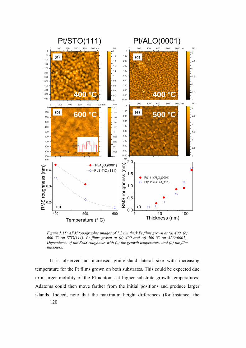
120
nm
0
0.2
0.4
0.6
0.8
1
1.2
1.4
1.6
1.8
20 100 200 300 400 500 nm
nm
0
50
100
150
200
250
300
350
400
450
500
550
nm
0
0.5
1
1.5
2
2.5
3
0 200 400 600 800 1000 nm
nm
0
100
200
300
400
500
600
700
800
900
1000
(a) (d)
400 ºC 400 ºC
Pt/STO(111) Pt/ALO(0001)
nm
0
0.2
0.4
0.6
0.8
1
1.2
1.4
1.6
1.8
20 200 400 600 800 1000 nm
nm
0
100
200
300
400
500
600
700
800
900
1000
nm
0
0.5
1
1.5
2
2.5
3
0 200 400 600 800 1000 nm
nm
0
100
200
300
400
500
600
700
800
900
1000
1 10 1000.0
0.5
1.0
1.5
2.0
Pt(111)/Al2O3(0001) Pt(111)/SrTiO3(111)
RM
S ro
ughn
ess
(nm
)
Thickness (nm)400 500 600
0.2
0.3
0.4 Pt/Al2O3(0001)Pt/SrTiO3(111)
RM
S ro
ughn
ess
(nm
)
Temperature (º C)
(b)
(c)
(e)
(f)
600 ºC 500 ºC
0 200 400 6000.0
0.5
1.0
1.5
2.0
Z (u
.c.)
X (nm)
Figure 5.15: AFM topographic images of 7.2 nm thick Pt films grown at (a) 400, (b) 600 ºC on STO(111). Pt films grown at (d) 400 and (e) 500 ºC on ALO(0001). Dependence of the RMS roughness with (c) the growth temperature and (b) the film thickness.
It is observed an increased grain/island lateral size with increasing
temperature for the Pt films grown on both substrates. This could be expected due
to a larger mobility of the Pt adatoms at higher substrate growth temperatures.
Adatoms could then move farther from the initial positions and produce larger
islands. Indeed, note that the maximum height differences (for instance, the

121
vertical scales are the same) for the images are not changed when growing the
films at higher growth temperature. Moreover, RMS roughness is lowered when
increasing the temperature (panel c). These observations are compatible with the
observed formation of multilayered islands with increased lateral size as
temperature increases. The formation of multilayered islands when increasing the
substrate temperature could be contradicting as the adatoms would then have
more energy to overcome the energy barrier and jump from a 2D island to a
bottom layer [San06]. However, it can be argued that multilayered island cannot
form at 400 ºC when the grains are too small. Finally, characterization of films
with varied thickness revealed a progressive increase in mound height and lateral
size with thickness. This morphology evolution resulted in a progressive increase
of the film roughness with thickness (panel f), raising the root-mean-square
roughness almost linearly from around 0.5 nm (for the t = 15.8 nm films) to above
1.5 nm for 180 nm thick films.
Summary and remarks of this section
Epitaxial Pt(111) oriented bottom electrodes were obtained by dc
sputtering on both STO(111) and ALO(0001). Laue oscillations are visible
denoting high crystal quality and smooth interfaces. There are two crystal
domains, 180 º in-plane rotated. The epitaxial relationships reveal that films are
under compressive in-plane stress induced by the substrate. As a result, thinner
films are strained, but a gradual relaxation is observed as thickness increases.
AFM images reveal a 2D growth mode, mound-like with increasing RMS
roughness as thickness increases and temperature decreases.
In parallel to the use of the Pt electrodes prepared by sputtering at CNRS-
ONERA, our group conducted efforts to produce equivalent electrodes at ICMAB.
Now we can produce Pt films of equivalent quality to the CNRS-ONERA ones
and, in fact, a few h-YMO samples presented in the next section were on our own-
made Pt electrodes.

122
5.1.3 Epitaxial h-YMO(0001) films on Pt(111) electrodes
In this section is described the growth and characterization by XRD, AFM
and TEM of the h-YMO(0001) films on top of Pt(111) buffered substrates. The
effect of YMO growth conditions and the use of differently thick Pt bottom
buffers are presented. The optimal preparation conditions for the h-YMO/Pt
bilayers are discussed.
h-YMO samples were grown by PLD on the Pt(111)-buffered STO(111)
and ALO(0001) substrates under the conditions described in Table 5.2. The
substrates were partially masked in order to allow later access to the bottom Pt
electrode. The series of samples fabricated allowed investigating the following
issues: firstly, the effect of the bottom Pt electrode thickness and, secondly, the
effect of the YMO deposition conditions on the structural properties of the films.
Batch/
Name
YMO
t (nm)
Pt
t (nm) Substrate T (ºC)
PO2
(mbar)
1/83A 90 3.6 ALO 800 0.2
1/83B 90 3.6 STO 800 0.2
1/ULB 90 7.2 STO 800 0.2
1/ULD 90 7.2 ALO 800 0.2
1/82A 90 14.4 ALO 800 0.2
1/82B 90 14.4 STO 800 0.2
1/98X 120 45 STO 800 0.2
1/98Z 120 45 ALO 800 0.2
2/111t 90 9.8 STO 800 0.1
2/b115 90 9.8 STO 785 0.1
2/114 90 9.8 STO 750 0.1
2/123 90 9.8 STO 700 0.1
3/R2A 120 17 ALO 650 0.1
3/R3A 120 17 ALO 700 0.1
3/R1A 120 17 ALO 750 0.1

123
15 35 55 75 95
ALO(0 0 0 12)ALO(0006)
STO(111)
Pt(111)
Pt(111)
STO(222)
Inte
nsity
(arb
. u.)
2θ (deg)
Pt(222
)
Pt(222
)
YMO(0008
)
YMO(0008
)
YMO(0006
)
YMO(0006
)
YMO(0004
)
YMO(0004
)
YMO(0002
)
YMO(0002
)
(b)
(a)
Figure 5.16: X-ray diffraction θ/2θ scans of YMnO3/Pt bilayers grown at 800 ºC and 0.2 mbar on (a) Al2O3(0001) and (b) SrTiO3(111) substrates. YMnO3 and Pt films are 90 and 14.4 nm thick, respectively.
Batch/
Name
YMO
t (nm)
Pt
t (nm) Substrate T (ºC)
PO2
(mbar)
4/152 90 19.6 STO 785 0.3
4/150 90 19.6 STO 785 0.2
4/157 90 19.6 STO 785 0.1
4/154 90 19.6 STO 785 0.02
5/S1 90 100 STO 785 0.1 Table 5.3: deposition conditions of the h-YMO films grown on Pt(111) buffered substrates. Samples labelled as R- were grown by R. Bachelet (ICMAB).
In Figure 5.16 are shown the θ/2θ scans of two selected samples: (a) h-
YMO/Pt/ALO(0001) and (b) h-YMO/Pt/STO(111). The h-YMO films were
grown at 800 ºC and PO2 = 0.2 mbar. The thickness of the films in these bilayers is
90 nm (h-YMO) and 14.4.nm (Pt). In addition to the substrate reflections, data in
Figure 5.16 show only peaks from (0001)-oriented h-YMO and (111)-oriented Pt
material. No traces of other phases and reflections were detected. Therefore, the
desired (0001) texture of h-YMO is obtained on Pt buffered ALO(0001) (panel a)
and STO(111) (panel b) substrates.
The effect of the bottom Pt buffer thickness on the growth of h-YMO is
addressed now. Figure 5.17 shows a zoom of the θ/2θ scans of samples grown at
800 ºC and 0.2 mbar with different thickness of the Pt bottom electrodes on (a)
ALO(0001) and on (b) STO(111) substrates. The thickness of the Pt layer is

124
30 35 40 452θ (deg)
45 nm
3.6 nm
7.2 nm
14.4 nm
ALO(0006)
Pt(111)hYMO(0004)In
tens
ity (a
rb. u
nits
)(a) (b)
30 35 40 452θ (deg)
o-YMO(202)
3.6 nm
7.2 nm
14.4 nm
45 nm
STO(111)Pt(111)
hYMO(0004)
800 ºC / 0.2 mbar 800 ºC / 0.2 mbar
Figure 5.17: XRD spectra of selected h-YMO samples grown at 800 ºC and 0.2 mbar on (a) Pt/ALO(0001) and (b) Pt/STO(111) substrates. Thickness of the Pt layer in each case is labelled next to the spectra. Vertical lines denote the bulk positions for the h-YMO and Pt(111) reflections
labelled next to each scan. It is observed that when Pt layer is 3.6 nm thick, the
diffracted intensity of the h-YMO(0004) reflection is very low and, moreover,
traces of the orthorhombic (101)-oriented peaks are detected on Pt/STO(111).
Recall that, in absence of Pt buffer, the orthorhombic phase is obtained on
STO(111) (further details in Appendix D). These traces of orthorhombic YMO are
not observed in the films grown Pt buffer layer with thickness equal or larger than
7.2 nm. It is worth mentioning at this point that a very recent work conducted in
collaboration with other members of the group has evidenced that dewetting of the
Pt can occur at high temperature [Bac09]. Note that the Pt layers (grown in the
400 – 600 C range) have been heated up to 800 ºC to grow the h-YMO films. The
degradation is especially strong when the Pt layer is thin [Bac09]. Thus, the
presence of traces of o-YMO is likely an indication that part of the film has grown
directly on the STO(111) substrate and part on the Pt(111) clusters formed. In the
same direction, it is worth noticing that the Laue fringes (which are signatures of
flat smooth surfaces) were preserved in the case of 14.4 nm thick Pt buffers even
after the deposition of h-YMO (~ 800 ºC), but disappeared when the Pt thickness
was thinner (that is, 7.2 and 3.6 nm). This observation evidences that the
dewetting is less strong if Pt films are thicker in agreement with Ref. [Bac09].
Of relevance here is that, after the deposition of the h-YMO layer at high

125
(a) (b)
30 35 40 45
Pt(111)hYMO(0004)
700 ºC
STO(111)
750 ºC
800 ºC
2θ (deg)30 35 40 45
650 ºC
2θ (deg)
ALO(0006)
700 ºC
Inte
nsity
(arb
. uni
ts)
750 ºC
Pt(111)hYMO(0004)
0.1 mbar / Pt: 9.8 nm0.1 mbar / Pt: 17 nm
Figure 5.18: XRD θ/2θ scan of selected h-YMO samples grown at 0.1 mbar and at different temperatures as labelled next to each spectra. The h-YMO films were grown on Pt(17nm)/ALO (panel a) and Pt(9.8nm)/STO (panel b). Vertical solid lines signal the bulk positions for h-YMO(0004) and Pt(111) reflections.
temperatures (800 ºC in Figure 5.17), the Pt(111) peaks appear at the bulk
positions (denoted by vertical solid line in Figure 5.17) in contrast to the shift to
lower angles observed for virgin Pt coatings (Figure 5.8). This is a signature that
the Pt layer is relaxed after the growth of the h-YMO layer. The h-YMO(0004)
peaks appear at the relaxed position on the thinner Pt layers (t < 45 nm) and
slightly shifted to higher angles on the thicker Pt layers (t = 45 nm). Discussion on
this observation will be presented later.
The role of the substrate temperature during the growth of h-YMO is
addressed in the following. Figure 5.18 shows the θ/2θ scans of h-YMO/Pt/ALO
(panel a) and h-YMO/Pt/STO (panel b). The h-YMO films were grown at 0.1
mbar and at the substrate temperature indicated in the labels next to each spectra.
The thickness of the h-YMO and Pt films were 120nm(h-YMO) / 17nm(Pt) and
90nm(h-YMO) / 9.8nm(Pt) for the h-YMO/Pt/ALO and h-YMO/Pt/STO bilayers,
respectively. As it was observed in the films grown directly on YSZ(111)
substrates, there is a minimum growth temperature were the h-YMO(0004) peaks
are observed. Irrespective of the bottom substrate, films grown at temperatures
above 700 ºC are clearly c-textured. The h-YMO(0004) reflections are slightly
shifted to higher angles thus indicating an small contraction of the out-of-plane
parameter. This contraction has also been observed in h-YMO films grown on

126
30 35 40 45
P = 0.02 mbar
2θ (deg)
P = 0.1 mbar
P = 0.2 mbar
Pt(111)hYMO(0004)
P = 0.3 mbar
STO(111)
785 ºC / Pt: 19.6 nm
Figure 5.19: PO2 dependence of the XRD spectra of h-YMO films, 90 nm thick, grown at 785 ºC grown at 785 ºC on Pt(19.6nm)/STO(111) substrates.
Pt/Si by MOCVD at similar substrate temperatures as reported by other authors
[Gel09]. This contraction of the c parameter is caused by the in-plane tensile
stress induced by the Pt layer as it will be commented later on the light of the φ-
scans. On both substrates (panels a and b in Figure 5.18), the angular location of
the h-YMO(0004) reflection and thus the value of the c parameter of h-YMO
remains essentially constant in the temperature range investigated. This could be
understood as the h-YMO grows on the bottom Pt layers which are similarly
relaxed (note the same angular positions for Pt(111) reflections in Figure 5.18).
Note that, as we saw for h-YMO/YSZ(111) films, the substrate temperature
changes did not reflect in changes in the c parameter (Figure 5.3).
One interesting aspect to note is that the Laue fringes have been preserved
for the h-YMO films grown at 800 ºC on Pt(9.8nm)/STO but are barely detected
in the h-YMO film grown at 750 ºC on Pt(17nm)/ALO. This fact suggests that the
degradation of the Pt layer is more evident for Pt coatings grown on ALO. Recent
work on the Pt dewetting issue supports this observation [Bac09].
The effect of the PO2 on the growth of the bilayers was also investigated.
Bilayers h-YMO(90nm)/Pt(19.6nm)/STO were grown at 785 ºC and at different
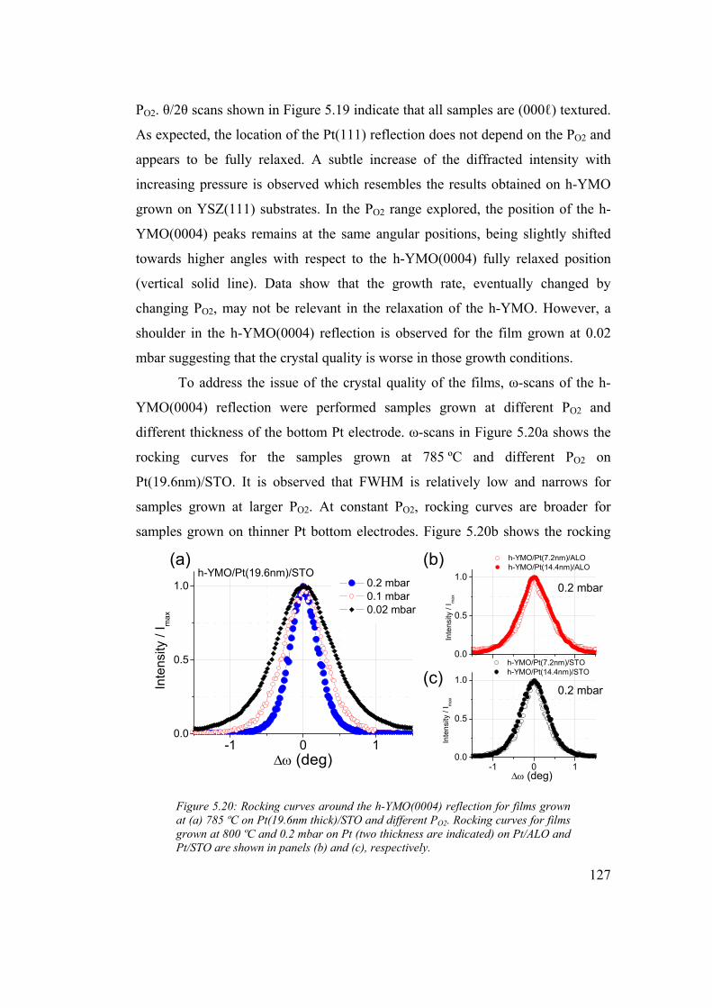
127
-1 0 10.0
0.5
1.0
h-YMO/Pt(7.2nm)/STO h-YMO/Pt(14.4nm)/STO
Inte
nsity
/ I m
ax
Δω (deg)
0.0
0.5
1.0
h-YMO/Pt(7.2nm)/ALO h-YMO/Pt(14.4nm)/ALO
Inte
nsity
/ I m
ax
(a) (b)
(c)
-1 0 10.0
0.5
1.0 0.2 mbar 0.1 mbar 0.02 mbar
Inte
nsity
/ I m
ax
Δω (deg)
h-YMO/Pt(19.6nm)/STO
0.2 mbar
0.2 mbar
Figure 5.20: Rocking curves around the h-YMO(0004) reflection for films grown at (a) 785 ºC on Pt(19.6nm thick)/STO and different PO2. Rocking curves for films grown at 800 ºC and 0.2 mbar on Pt (two thickness are indicated) on Pt/ALO and Pt/STO are shown in panels (b) and (c), respectively.
PO2. θ/2θ scans shown in Figure 5.19 indicate that all samples are (000ℓ) textured.
As expected, the location of the Pt(111) reflection does not depend on the PO2 and
appears to be fully relaxed. A subtle increase of the diffracted intensity with
increasing pressure is observed which resembles the results obtained on h-YMO
grown on YSZ(111) substrates. In the PO2 range explored, the position of the h-
YMO(0004) peaks remains at the same angular positions, being slightly shifted
towards higher angles with respect to the h-YMO(0004) fully relaxed position
(vertical solid line). Data show that the growth rate, eventually changed by
changing PO2, may not be relevant in the relaxation of the h-YMO. However, a
shoulder in the h-YMO(0004) reflection is observed for the film grown at 0.02
mbar suggesting that the crystal quality is worse in those growth conditions.
To address the issue of the crystal quality of the films, ω-scans of the h-
YMO(0004) reflection were performed samples grown at different PO2 and
different thickness of the bottom Pt electrode. ω-scans in Figure 5.20a shows the
rocking curves for the samples grown at 785 ºC and different PO2 on
Pt(19.6nm)/STO. It is observed that FWHM is relatively low and narrows for
samples grown at larger PO2. At constant PO2, rocking curves are broader for
samples grown on thinner Pt bottom electrodes. Figure 5.20b shows the rocking
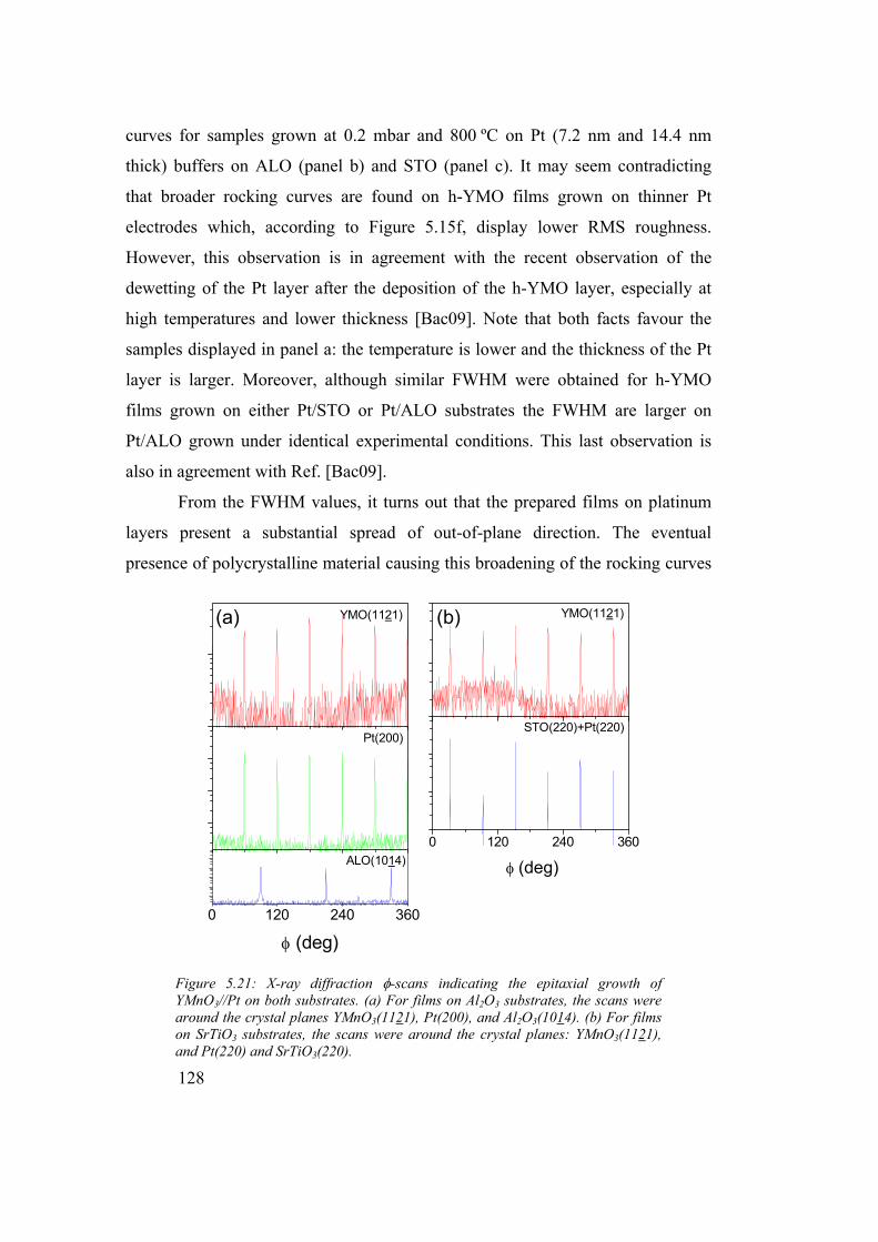
128
YMO(1121)
ALO(1014)
Pt(200)
(b)(a) YMO(1121)
STO(220)+Pt(220)
0 120 240 360
φ (deg)
0 120 240 360
φ (deg)
Figure 5.21: X-ray diffraction φ-scans indicating the epitaxial growth of YMnO3//Pt on both substrates. (a) For films on Al2O3 substrates, the scans were around the crystal planes YMnO3(1121), Pt(200), and Al2O3(1014). (b) For films on SrTiO3 substrates, the scans were around the crystal planes: YMnO3(1121), and Pt(220) and SrTiO3(220).
curves for samples grown at 0.2 mbar and 800 ºC on Pt (7.2 nm and 14.4 nm
thick) buffers on ALO (panel b) and STO (panel c). It may seem contradicting
that broader rocking curves are found on h-YMO films grown on thinner Pt
electrodes which, according to Figure 5.15f, display lower RMS roughness.
However, this observation is in agreement with the recent observation of the
dewetting of the Pt layer after the deposition of the h-YMO layer, especially at
high temperatures and lower thickness [Bac09]. Note that both facts favour the
samples displayed in panel a: the temperature is lower and the thickness of the Pt
layer is larger. Moreover, although similar FWHM were obtained for h-YMO
films grown on either Pt/STO or Pt/ALO substrates the FWHM are larger on
Pt/ALO grown under identical experimental conditions. This last observation is
also in agreement with Ref. [Bac09].
From the FWHM values, it turns out that the prepared films on platinum
layers present a substantial spread of out-of-plane direction. The eventual
presence of polycrystalline material causing this broadening of the rocking curves
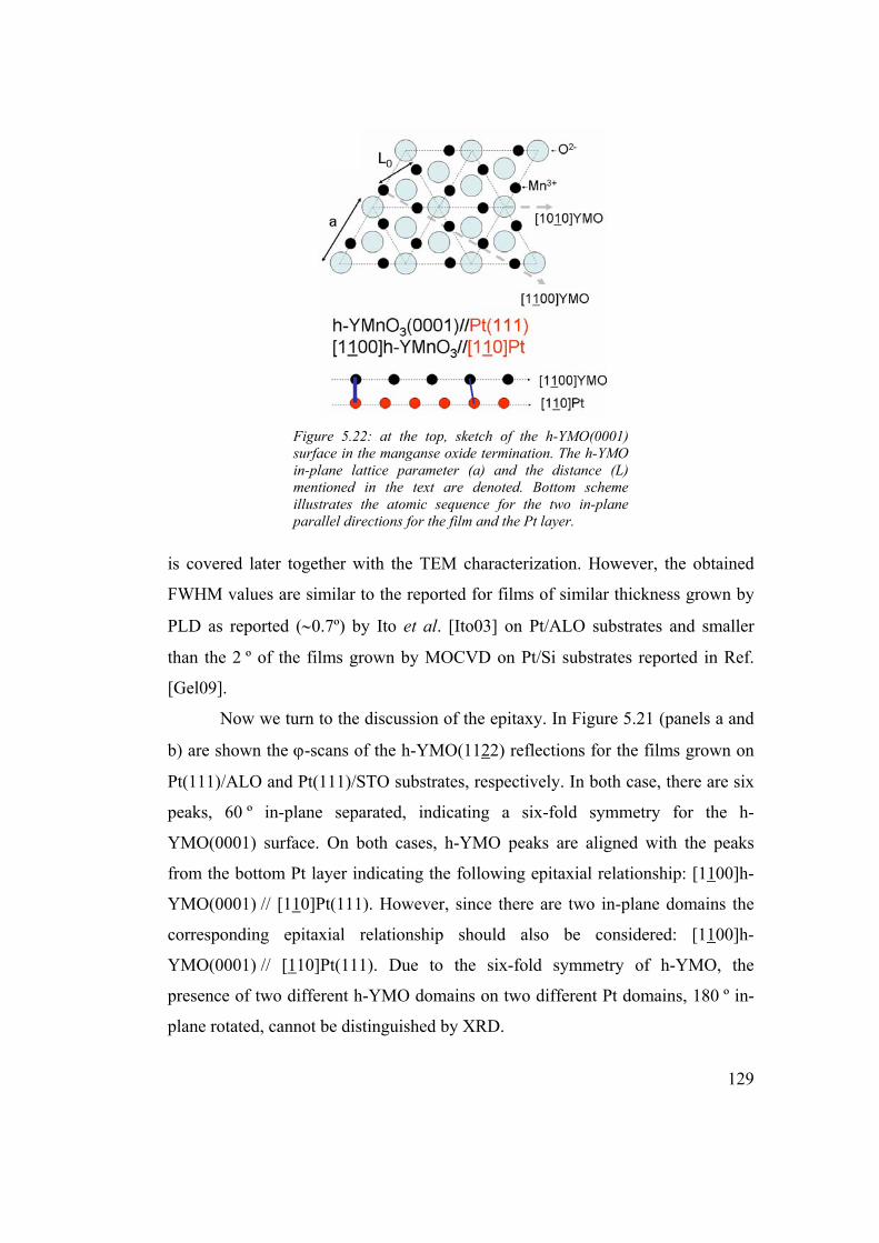
129
Figure 5.22: at the top, sketch of the h-YMO(0001) surface in the manganse oxide termination. The h-YMO in-plane lattice parameter (a) and the distance (L) mentioned in the text are denoted. Bottom scheme illustrates the atomic sequence for the two in-plane parallel directions for the film and the Pt layer.
is covered later together with the TEM characterization. However, the obtained
FWHM values are similar to the reported for films of similar thickness grown by
PLD as reported (∼0.7º) by Ito et al. [Ito03] on Pt/ALO substrates and smaller
than the 2 º of the films grown by MOCVD on Pt/Si substrates reported in Ref.
[Gel09].
Now we turn to the discussion of the epitaxy. In Figure 5.21 (panels a and
b) are shown the ϕ-scans of the h-YMO(1122) reflections for the films grown on
Pt(111)/ALO and Pt(111)/STO substrates, respectively. In both case, there are six
peaks, 60 º in-plane separated, indicating a six-fold symmetry for the h-
YMO(0001) surface. On both cases, h-YMO peaks are aligned with the peaks
from the bottom Pt layer indicating the following epitaxial relationship: [1100]h-
YMO(0001) // [110]Pt(111). However, since there are two in-plane domains the
corresponding epitaxial relationship should also be considered: [1100]h-
YMO(0001) // [110]Pt(111). Due to the six-fold symmetry of h-YMO, the
presence of two different h-YMO domains on two different Pt domains, 180 º in-
plane rotated, cannot be distinguished by XRD.

130
2.0 2.5 3.07.6
8.0
8.4
hYMO(3038)hYMO(2028)
Pt(113)
Qx [1010]h-YMO (r.l.u.)
Qy
[000
1]h-
YM
O (r
.l.u.
)
ALO(1129)
2.0 2.5 3.0
8.0
8.5STO(113)
hYMO(3038)
Pt(113)
Qx [1010]h-YMO (r.l.u.)
Qy
[000
1]h-
YMO
(r.l.
u.)
(a) (b)
Figure 5.23:.Reciprocal space of two h-YMO samples around the substrate (1129) and (113) reflections of (a) ALO and (b) STO respectively. Samples were grown at 800 ºC, 0.2 mbar. h-YMO and Pt films are 120 nm and 45 nm thick, respectively.
The lattice mismatch picture is depicted in Figure 5.22. The h-YMO(0001)
surface in the manganse oxide termination is sketched. The [1100]h-YMO and the
[1010] directions are denoted. Of relevance here is that, according to the epitaxial
relationships, the [1100]h-YMO direction must be parallel to [110]Pt. The
corresponding atomic sequences for each direction in each material are depicted in
bottom sketches. The arrangement found (Figure 5.22, bottom) suggests that a
multi-cell matching must occur. The minimum atom-to-atom mismatch is found
when four cations in the h-YMO film are related to five atoms of the Pt lattice. In
this arrangement, the lattice mismatch is as low as 2.09%. According to this lattice
mismatch, the h-YMO films are under tensile stress and, as a consequence, an
expansion of the in-plane parameters and a contraction of the out-of-plane
parameter is expected. The c expansion has already been observed in the θ/2θ
scans as a small shift of the h-YMO(0004) peaks towards higher angular
positions. The in-plane parameters are discussed in next paragraph.
Reciprocal space mapping was used to determine the in-plane parameters.
The chosen reflections to collect were the following: ALO(1129) or STO(113) for
the substrate, Pt(113), and h-YMO(308). In Figure 5.23 (panel a) is shown the
reciprocal space map for a selected sample on ALO substrate (98Z). Note that the
Pt(113) peak is visibly shifted from the Qx location of the substrate reflection
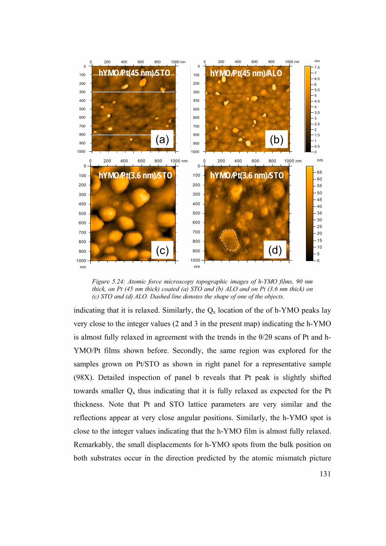
131
nm
0
1
2
3
4
5
6
7
8
9
100 200 400 600 800 1000 nm
nm
0
100
200
300
400
500
600
700
800
900
1000
nm
0
1
2
3
4
5
6
7
8
9
100 200 400 600 800 1000 nm
nm
0
100
200
300
400
500
600
700
800
900
1000
(a)
nm
00.511.522.533.544.555.566.577.5
0 200 400 600 800 1000 nm
nm
0
100
200
300
400
500
600
700
800
900
1000
nm
00.511.522.533.544.555.566.577.5
0 200 400 600 800 1000 nm
nm
0
100
200
300
400
500
600
700
800
900
1000
(b)
hYMO/Pt(45 nm)/STO
nm
0510152025303540455055606570
0 200 400 600 800 1000 nm
nm
0
100
200
300
400
500
600
700
800
900
1000
(c)
hYMO/Pt(3.6 nm)/STO
hYMO/Pt(45 nm)/ALO
nm
051015
20253035404550
556065
0 200 400 600 800 1000 nm
nm
0
100
200
300
400
500
600
700
800
900
1000
(d)
hYMO/Pt(3.6 nm)/STO
Figure 5.24: Atomic force microscopy topographic images of h-YMO films, 90 nm thick, on Pt (45 nm thick) coated (a) STO and (b) ALO and on Pt (3.6 nm thick) on (c) STO and (d) ALO. Dashed line denotes the shape of one of the objects.
indicating that it is relaxed. Similarly, the Qx location of the of h-YMO peaks lay
very close to the integer values (2 and 3 in the present map) indicating the h-YMO
is almost fully relaxed in agreement with the trends in the θ/2θ scans of Pt and h-
YMO/Pt films shown before. Secondly, the same region was explored for the
samples grown on Pt/STO as shown in right panel for a representative sample
(98X). Detailed inspection of panel b reveals that Pt peak is slightly shifted
towards smaller Qx thus indicating that it is fully relaxed as expected for the Pt
thickness. Note that Pt and STO lattice parameters are very similar and the
reflections appear at very close angular positions. Similarly, the h-YMO spot is
close to the integer values indicating that the h-YMO film is almost fully relaxed.
Remarkably, the small displacements for h-YMO spots from the bulk position on
both substrates occur in the direction predicted by the atomic mismatch picture

132
20 nm
YMO
Pt
STO
STO [1 -1 0]
(1 1 1)
(1 1 0)
(0 0 1)
Pt [1 -1 0](-1 -1 1)
YMO [1 -1 0]
(1 1 -1)(1 1 0)
(0 0 1)
5 nm
YMOPt
STO
5 nm
YMOPt
STO
(a) (b)i
ii
iii
(i) (ii) (iii)
(1 1 1)
Figure 5.25: (a) Cross-section TEM image of a h-YMO/Pt/STO sample. Three regions of this image have been investigated by electron diffraction and are shown below in panels (i), (ii), and (iii). (b) shows a HRTEM image indicating sharp interfaces h-YMO/Pt and Pt/STO.
shown in Figure 5.22: Qy is increased (c elongated) and Qx is reduced (a
contracted).
Topographic AFM images of the YMO films (120 nm thick) grown on 45
nm thick Pt coated STO(111) and ALO(0001) are shown in Figure 5.24. The
multilayered island character from the bottom Pt electrode is preserved. This
morphology is particularly evident in Figure 5.24b. The images also reveal the
presence of particulates and nanocrystals, some of them hexagonally shaped.
These crystals most likely to be h-YMO crystallites can be up to around 100 nm
long and up to 10 nm high. However as Pt thickness decreases the size of these
3D h-YMO nanocrystallites increases, reaching in the case of the thinnest layers
up to 50 nm in a 90 nm thick film. It turns out that Pt buffers should be as thicker
as possible. This conclusions is directly linked with the recent work on the Pt

133
1 nm[0001]
Figure 5.26: Zoom of Figure 5.25b showing the stacking of MnO5 and YO7 layers along the [0001]YMnO3 direction.
dewetting [Bac09] commented early in this section.
Finally, the TEM characterization is presented. Figure 5.25a displays the
TEM image for a 90 nm thick h-YMO film grown on a Pt-buffered (14.4 nm
thick) STO substrate. There are observed sharp interfaces at least along the 250
nm covered by the picture. Electron diffraction patterns of three regions labelled
(i), (ii), and (iii) are showed below. There are clear diffraction spots in Pt and h-
YMO layers without traces of circles (polycrystalline material) and/or secondary
orientations in the regions investigated. The spots can be indexed as shown in the
Figure. The out-of-plane direction is signalled by an arrow. Then, the epitaxial
relationship is (001)h-YMO[110]/(111)Pt[110]/(111)STO[110] in agreement with
the one found by XRD and sketched in Figure 5.22.
In order to get a better insight into the crystallographic properties of these
heterostructures, a HRTEM study has been carried out on this YMO/Pt/STO(111)
sample. In the cross section image of Figure 5.25b it can be appreciated that the Pt
buffer layer has a thickness of about 15.8 nm, in good agreement with data
extracted from X-ray analysis. In the explored region, the YMO appears to be of
high crystal quality. The stacking of MnO5 and YO7 polyhedral layers along the
[0001] direction are perfectly resolved as shown in Figure 5.26. However, this
crystal quality contrasts with the broadening observed in the rocking curves and

134
(a) (b)
STO(200)
hYMO(1124)
hYMO(1122)
STO(110)
STO(100)
STO(111)
hYMO(1012)⇒
hYMO(2012)⇒
Figure 5.27: (a) Added-frame plot revealing the absence of polycrystalline material. (b) Pole Figure revealing the in-plane epitaxy showing the two in-plane Pt domains (labelled A and B) but no further traces of in-plane disorder. (Sample 82).
the presence of h-YMO nanocrystals at the surface as observed in the topographic
AFM images. Due to the locality of TEM analyses, the existence of a certain
disorder at a longer range can not be completely ruled out. This disorder may be
caused by random inclusions and/or polycrystalline material. To investigate this
possibility, XRD by a 2-dimensional detector frames were collected (Figure
5.27a) as well as pole figures (Figure 5.27b) with relatively large acquisition
times. The presence of polycrystalline material would appear as vertical
elongation of the h-YMO peaks in the XRD frames (Figure 5.27a), which are not
present. Similarly, in Figure 5.27b in-plane disorder would be evidenced by
continuous intensity along ϕ angle. Instead, the diffraction peaks appear at very
localized positions. Within the limitations of XRD, signatures accounting for
eventual microstructural disorder are not detected.
Summary of this section
Single phase hexagonal YMO(0001) grows on Pt(111) electrodes if the
electrodes are at least 7 nm thick. A minimum temperature of 700 ºC has been
determined for the c-textured growth of h-YMO films. XRD did not evidence
clear trends for films grown at different PO2 or temperature (as long as T ≥ 700
ºC). Films are epitaxial as evidenced by pole figures and ϕ-scans with the
135
relationship: [1100]YMO(0001) // [110]Pt(111). Pt in-plane lattice parameters are
fully relaxed. h-YMO in-plane parameters are slightly elongated. Surface
morphology preserves the 2D island growth from the bottom Pt layer with an
increasing presence of nanocrystals as Pt thickness decreases. TEM images of the
h-YMO/Pt/STO films reveal sharp interfaces, at least along 250 nm, and HRTEM
shows in a local scale a defect-free stacking of the (000ℓ) planes of the h-YMO.
5.1.4 Growth of top Py electrode
Permalloy (Py, Ni80:Fe20) was deposited on former h-YMO/Pt/Substrates
bilayers by sputtering. The depositions were performed firstly at CNRS-ONERA
by U. Lüders and J.F. Bobo [sample UL-B]. Lately, the growth of Py was
developed at FAO - Universitat de Barcelona by M. Rubio and E. Bertran and
some coatings were performed there [sample S1]. The deposition conditions there
were kept as similar as possible to the CNRS-ONERA ones.
Previous to deposition, 6.6 mTorr pure Ar were introduced in the chamber.
The substrate was placed on-axis at 10 cm and an static magnetic field of 100 Oe
is applied in-plane of the sample. Then, the target was pre-sputtered for 10
minutes before starting the deposition and, subsequently, films were sputtered at
room temperature. Py thickness was 15 nm. During the Py growth, the samples
were partially covered by physical mask in order to define a desired area of Py on
top of h-YMO with no short-circuits with bottom Pt electrodes.
5.2 Functional characterization
The objective of this section is to describe the experiments and the results
where the magnetization of the top Py electrode is controlled by an electric field.
Section starts with the resistivity measurements performed on a set of h-YMO
films grown at different conditions. Then the existence of exchange bias at the
interface of the Py/h-YMO structure is demonstrated by SQUID magnetometry
and AMR experiments. Next, the effects of an applied electric field on the
exchange bias are discussed.
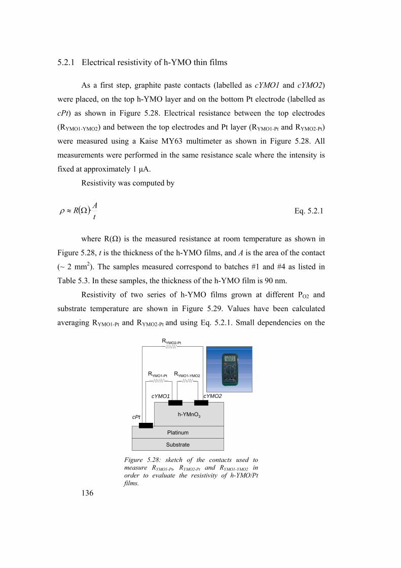
136
Substrate
Platinum
h-YMnO3cPt
cYMO1 cYMO2
RYMO2-Pt
RYMO1-Pt RYMO1-YMO2
Figure 5.28: sketch of the contacts used to measure RYMO1-Pt, RYMO2-Pt and RYMO1-YMO2 in order to evaluate the resistivity of h-YMO/Pt films.
5.2.1 Electrical resistivity of h-YMO thin films
As a first step, graphite paste contacts (labelled as cYMO1 and cYMO2)
were placed, on the top h-YMO layer and on the bottom Pt electrode (labelled as
cPt) as shown in Figure 5.28. Electrical resistance between the top electrodes
(RYMO1-YMO2) and between the top electrodes and Pt layer (RYMO1-Pt and RYMO2-Pt)
were measured using a Kaise MY63 multimeter as shown in Figure 5.28. All
measurements were performed in the same resistance scale where the intensity is
fixed at approximately 1 μA.
Resistivity was computed by
( )tAR ·Ω≈ρ Eq. 5.2.1
where R(Ω) is the measured resistance at room temperature as shown in
Figure 5.28, t is the thickness of the h-YMO films, and A is the area of the contact
(~ 2 mm2). The samples measured correspond to batches #1 and #4 as listed in
Table 5.3. In these samples, the thickness of the h-YMO film is 90 nm.
Resistivity of two series of h-YMO films grown at different PO2 and
substrate temperature are shown in Figure 5.29. Values have been calculated
averaging RYMO1-Pt and RYMO2-Pt and using Eq. 5.2.1. Small dependencies on the

137
0.0 0.1 0.2 0.30.0
0.5
1.0T = 785 ºC
ρ (M
Ω·c
m)
PO2 (mbar)700 750 800
Growth temperature (ºC)
P = 0.1 mbar (c)(a) (b)
300
Figure 5.29: resistivity of the samples as a function of the (a) PO2 or (b) the substrate temperature during the deposition.(c) Resistivity measurements in h-YMO single crystals [Kat01].
deposition conditions are observed but the resistivity values are rather constant
around 0.25 MΩ·cm. The measured resistivity of the h-YMO films is only slightly
smaller than the reported resistivity for bulk h-YMO single crystals (Figure 5.29c)
[Kat01].
Values for RYMO1-Pt and RYMO2-Pt were found to be different thus indicating
a non homogenous resistivity sample. In the worst case, differences were larger
than 50%. This spread in the resistance values in each top electrode could be
caused by the presence of the nanocrystals observed in the AFM characterization
if they were not homogeneously distributed in the surface. In that situation, the
use of smaller contacts would boost the chances to cover defect-free regions on
the h-YMO layer. To investigate this issue, a set of 20 Pt contacts (0.2 mm2) were
deposited on top of sample 157 (grown at 785 ºC and 0.1 mbar on
Pt(19.6nm)/STO). With the smaller (0.2 mm2) Pt contacts and measuring with the
same multimeter, it was found that ρ ~ 4.3 ± 1.2 MΩ·cm. Therefore, the resistivity
measured using the 0.2 mm2 Pt contacts is one order of magnitude larger than in
the previous measurements shown in Figure 5.18 where the contact area was 2
mm2. However, it is noticed that the standard deviation of the resistivity (more
than 25% of the central value) is very large confirming the non homogeneity of
the resistivity. Recall that AFM revealed that the nanocrystallites could present a
typical lateral size of 100 nm and a density of 10 crystals per μm2. If the low
resistivity was caused by the crystallites, either the size of the electric contacts
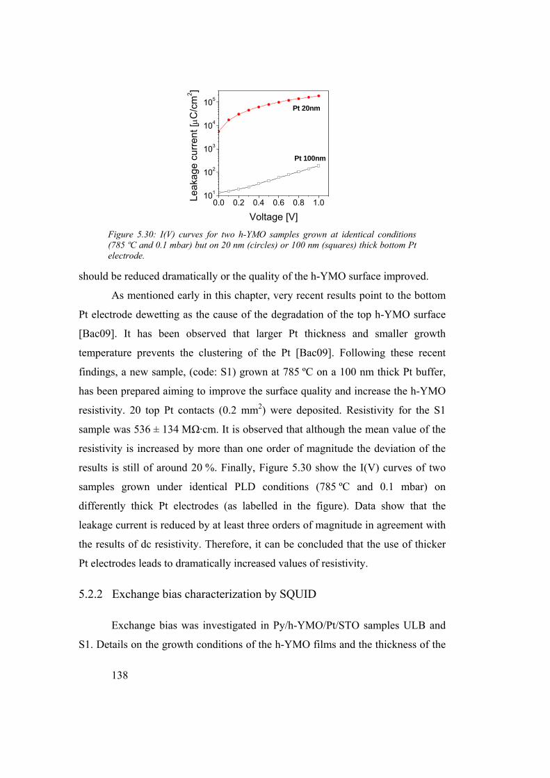
138
0.0 0.2 0.4 0.6 0.8 1.0101
102
103
104
105
Pt 100nm
Pt 20nm
Leak
age
curr
ent [
μC/c
m2 ]
Voltage [V] Figure 5.30: I(V) curves for two h-YMO samples grown at identical conditions (785 ºC and 0.1 mbar) but on 20 nm (circles) or 100 nm (squares) thick bottom Pt electrode.
should be reduced dramatically or the quality of the h-YMO surface improved.
As mentioned early in this chapter, very recent results point to the bottom
Pt electrode dewetting as the cause of the degradation of the top h-YMO surface
[Bac09]. It has been observed that larger Pt thickness and smaller growth
temperature prevents the clustering of the Pt [Bac09]. Following these recent
findings, a new sample, (code: S1) grown at 785 ºC on a 100 nm thick Pt buffer,
has been prepared aiming to improve the surface quality and increase the h-YMO
resistivity. 20 top Pt contacts (0.2 mm2) were deposited. Resistivity for the S1
sample was 536 ± 134 MΩ·cm. It is observed that although the mean value of the
resistivity is increased by more than one order of magnitude the deviation of the
results is still of around 20 %. Finally, Figure 5.30 show the I(V) curves of two
samples grown under identical PLD conditions (785 ºC and 0.1 mbar) on
differently thick Pt electrodes (as labelled in the figure). Data show that the
leakage current is reduced by at least three orders of magnitude in agreement with
the results of dc resistivity. Therefore, it can be concluded that the use of thicker
Pt electrodes leads to dramatically increased values of resistivity.
5.2.2 Exchange bias characterization by SQUID
Exchange bias was investigated in Py/h-YMO/Pt/STO samples ULB and
S1. Details on the growth conditions of the h-YMO films and the thickness of the

139
-5
0
5T = 2 K
2nd
m (1
0-5 e
mu)
1st
-100 0 100
-10
0
10
m (1
0-5 e
mu)
Field (Oe)
T = 2 K
2nd1st
-100 0 100
T = 100 K
Field (Oe)
T = 100 K
(a) (b)
(c) (d)
Figure 5.31: Magnetization loops at 100 K of samples (b) ULB and (d) S1 samples. Magnetization loops afterFC from 100 K to 2 K at 3000 Oe of samples (a) ULB and (c) S1. Names of the samples correspond to Table 5.3.
Pt and h-YMO layers are presented in Table 5.3. In the first sample (ULB) both
electrodes were deposited at CNRS-ONERA, while in the second sample (S1) top
Py electrode was deposited at FAO-Universitat de Barcelona and bottom Pt
electrode at ICMAB. The observation of the exchange bias and its magnitude are
found to be independent of the set-up used for electrode deposition.
Figure 5.20 display the magnetization loops of samples (b) UL-B and (d)
S1 at 100 K. As this temperature is higher than TN in h-YMO, no exchange bias
effects are expected. Indeed, the loops measured at T = 100 K > TN after a FC
from 300 K at 3000 Oe are symmetric with coercivity (HC) of only ∼10 Oe. Figure
5.31 (panels a and c) shows loops were measured at 2 K after a FC from 100 K at
3000 Oe. In contrast, at T < TN, the loops (panels a and c) are broadened and
asymmetric, revealing that an exchange bias accompanied by a significant
coercivity enhancement develops at low temperatures. In two magnetization loops
measured consecutively (denoted 1st and 2nd), it can be appreciated that there is a
significant reduction of HEB upon cycling the field known as training effect (see
Chapter 2).
The values for the exchange bias (Heb) and the coercitive field (Hc) are
shown in Figure 5.32a showing very similar dependency with the temperature in
both samples. It is noticed that Heb decays very rapidly and vanishes at ~ 10 K.

140
0 10 20 80 100-10
-5
0
5
10
82B S1
m (1
0-5 e
mu)
Temperature (K)
H = - 70 Oe(a) (b)
1 10 1000
25
50
75
100
0
25
50
75
100
Hc
(Oe)
Heb
(Oe)
Temperature (K)
Heb(Oe) ULB S1
Hc (Oe) ULB S1
ULBS1
Figure 5.32: (a) Exchange bias and coercitivity as a function of the temperature for two samples. (b) Temperature dependence of the magnetization at H = - 70 Oe after FC from 100 K at 3000 Oe.
This fact indicates that the magnetic anisotropy induced by the FC (that is, the
Heb) disappears at ~ 10 K.
The temperature dependence of the magnetization after FC measured at a
fixed magnetic field larger than the Py coercitivity provides a supplementary
proof of the gradual vanish of the Heb as temperature increases. As shown in
Figure 5.31, at 2 K (panels a and c) the magnetization of the Py is still positive
even though the external magnetic field is larger than its coercitivity field (10 Oe
at 100 K where exchange bias is not present). As it is shown in Figure 5.32b,
departing from 2 K and heating up while keeping constant the magnetic field (- 70
Oe) the Py magnetization gradually reverses. The maximum reversal achieved is
reached at 10 K for both samples as if Heb was absent and the Py magnetization
just followed the external (negative) magnetic field. As a consequence, in the
magnetometry set-up, exchange bias effects will only be visible below 10 K.
5.2.3 Exchange bias characterization by anisotropic magnetoresistance
As described in Chapter 2, the exchange bias provokes changes of the
anisotropic magnetoresistance (AMR) of the upper Py layer. A sketch of the
measurement is presented in Figure 5.33. AMR was measured for sample UL-B
by rotating the magnetic field in the film plane while recording the film resistance
R as a function of the angle θ between the measuring current and the applied
magnetic field (Ha = 40 Oe). Further details are described in Section 3.2.4.

141
Pt
Side view Top view
Py
Figure 5.33: Sketch of the multilayer structure in the AMR measurement. Contacts and direction of the magnetic field and current are displayed.
Prior to any measurement, the sample was field cooled (3 kOe at θa =
θeb = 45 º) from room temperature to the measuring temperature and then the field
was reduced to the selected Ha value. In Figure 5.34 are shown the R(θ) cycles
recorded at several temperatures, above and below TN (∼70 K). Note that this Ha =
40 Oe value is smaller that the largest Hc value determined from the
magnetization loops.
At T = 100 K, R(θ) displays the common cos2θ dependence expected for a
system where the magnetization follows the magnetic field. However, at 50K,
R(θ) displays a clear departure of the cos2θ dependence due to the presence of the
Heb, which becomes more prominent when cooling down. In fact, at 2 K the
presence of an Heb has dramatically modified the magnetization response when Ha
is rotated. This strong departure of the R(θ) curve from the cos2θ dependence
indicates that, at 2K, Heb should be much larger than the measuring field (Ha =
40 Oe). Therefore, it turns out that the exchange bias is larger in AMR
measurements than the values extracted from SQUID magnetometry loops.
Observation of larger Heb values in transport measurements results from
the different way in which the presence of the exchange bias is revealed. The
difference is due to the fact that in magnetization measurements, exchange-bias
monitoring requires a 180 º magnetization switching whereas in AMR
measurements this is not required: only small reversible movements of the
magnetization around Heb can be used to probe the existence of a finite exchange
bias. This reason also accounts for the absence of hysteresis in measurements

142
0 60 120 180 240 300 360
21.20
21.21
θa (deg)
T=10 K
21.31
21.32
T=6 K
21.59
21.61
T=2 K
R (Ω
)
0 60 120 180 240 300 360
21.32
21.33
T=100 K
θa (deg)
21.25
21.26
T=50 K
21.11
21.12
T=15 K
R (Ω
)
Figure 5.34: Angular dependence of the magnetoresistance (AMR) of the Py film at several temperatures. Measurements were done under a 40 Oe magnetic field, and after field-cooling (from 3 kOe) applied at 45º with respect to the measuring current.
performed at the lowest temperature (Figure 5.22a) as the magnetic anisotropy is
large and M remains confined within an energy minimum while Ha rotates; at
intermediate temperatures hysteresis is evident as M is dephased with respect to
Ha.
By the same token, hysteresis in AMR curves at a certain temperature is
only observed when Ha ~ Heb. In Figure 5.35a are shown curves recorded at the
same temperature but with different magnetic fields. Reversible AMR is found for
the Ha >> Heb and vice versa. However, hysteresis appears at intermediate fields.
The Ha which displays the larger hysteresis at each temperature could be used as a
signature of the order of magnitude of Heb. For instance, at 5 K, from AMR it
could be estimated that Heb ~ 100 Oe which is approximately three times larger
than in magnetometry.
Previous methods to qualitatively extract the exchange bias required the
observation of the evolution of the AMR hysteresis with the temperature or Ha in
a set of curves. A method to extract the exchange bias from a single AMR curve is
described now. Using the simple geometrical model of field addition as described
in work by Miller et al. [Mil96], it is possible to extract Heb directly from one
measured R(θa) curve. The use of this simple model, though, is limited to when
the response is reversible. When hysteresis in the AMR response appears, the
model is ineffective. Despite this fact, an order of magnitude can be estimated by

143
0 60 120 180 240 300 36018.41
18.42
18.43
50 OeR (Ω
)
θa (deg)
18.41
18.42
18.43
100 OeR (Ω
)
18.41
18.42
18.43
500 Oe
R (Ω
)
(a)0 120 240 360
21.20
21.21
21.22
21.23
21.24
4
3
2
RPy
(Ω)
θa (deg)
1
(b)
Figure 5.35: (a) Angular dependence of the magnetoresistance of the Py at several magnetic fields and temperature fixed at 5 K. (b) Fitting of some of the AMR curves in order to extract Heb.
fitting the AMR according to Eq. 2.7 in Chapter 2. Fits are shown in Figure 5.35b
as solid lines through the experimental points for the clockwise rotation of some
representative R(θa) curves. The extracted values for Heb are 270±40 (5 K),
220±20 (5 K), 0.2±0.6 (50 K) and 0 Oe (100 K) for the curves labelled as 1, 2, 3,
and 4 respectively.
5.3 Electric-field effect on the magnetic properties
In the previous section has been shown that at the Py/h-YMO interface
exchange bias is present. Since the h-YMO(0001) is a fully compensated surface,
the net magnetic moment required for the exchange bias could arise from the
antiferromagnetic domain walls. On the other hand, the work of Fiebig et al.
indicated that the ferromagnetic and antiferromagnetic domain walls in h-YMO
were coupled [Fie02]. Therefore, the manipulation of the ferroelectric domain
walls by electric field is expected to drag as well the antiferromagnetic domain
walls and, in turn, the exchange bias.
This hypothesis has been investigated in the present thesis by biasing the

144
-300 -200 -100 0 100 200 300-8
-4
0
4
8
Ve= 0V
Ve= 1.2V
m (1
0-5 e
mu)
H (Oe)
Ve= 0.6V
(a)
0 120 240 36020.3520.3620.37
Ve=1.8 V
θa (deg)
20.4520.4620.47
Ha = 50 Oe
Ha = 50 Oe
Ve=1.2 V
R (Ω
)
21.2221.2321.24
Ve=0
(b) Ha = 50 Oe
Figure 5.36: (a) Magnetization loops of Py/YMO/Pt, measured at 2 K, after cooling the sample from 300 K in 3 kOe field, under various biasing-voltage (Ve) values. (b) AMR of the Py film when biasing the Py/YMO/Pt sandwich by an electric field. Measurements were done at 5 K in magnetic field of 50 Oe, after field-cooling (3 kOe) and applying Ve = 0, 1.2 and 1.8 V.
h-YMO sandwiched between top Py and bottom Pt electrodes. Experiments on
two Py/h-YMO/Pt samples (labelled UL-B and S1) are presented in this section.
Their resistivity is 2.2 MΩ·cm (UL-B) and 536 MΩ·cm (S1), measured as
described in section 5.2.1 using two contacts with areas 2 mm2 and 0.2 mm2,
respectively.
The results will show that electrical bias modifies the exchange bias. First
are shown the results of the electric field effects of a dc electric field in
magnetometry and AMR measurements using sample UL-B. In the second part of
this section, exchange bias is modified via electric pulses using sample S1.
5.3.1 Electric dc field effects on the exchange bias
Figure 5.36a shows the magnetization loops of sample UL-B, at 2 K, under
various biasing-voltages (Ve), after field-cooling (3 kOe) the sample from 300 K.
In the unbiased sample (Ve = 0), there is a clear shift of the loop which reflects the
existence of an exchange bias field Heb (≈ 60 Oe). When applying a biasing-
voltage across the h-YMO layer, the shift of the M(H) loop gradually disappears
and for Ve = 1.2 V the loop is symmetric and narrower thus indicating the
suppression of Heb and the coercivity.
The suppression of exchange bias upon biasing the sample was also

145
monitored in this sample by AMR experiments. Figure 5.36b shows the data
recorded at 5 K (with Ha = 50 Oe, and after 3 kOe field-cooling from 300 K, at
45 º) at some selected biasing-voltages. The data reveal a important modification
of R(θa). The unbiased measurement (Ve = 0) resembles the AMR curves where
the exchange bias field is larger than the external magnetic field. In this case, the
exchange bias should be clearly larger than 50 Oe. Note, for instance, that when
increasing Ve, a second R(θa) minimum at about ∼270º emerges. Comparison of
the biased and un biased R(θa) curves indicates that upon electric-field biasing the
Heb becomes relatively less relevant on the R(θa) response. That is, the electric
field mimics the effect of increasing the temperature or, alternatively, the applied
magnetic field Ha.
The two precedent measurements indicate that the electric biasing is
equivalent to a reduction of the exchange bias. One interesting experiment is to
investigate the magnetization of the top Py layer (MPy) under an applied magnetic
field (Ha) along the opposite direction and larger than the coercitivity field (Hc). A
switching of the magnetization will occur if:
|Ha| > |Heb| + |Hc| Eq. 5.3.1
Since in this experiment |Ha| > |Hc| is chosen, MPy is hold “positive” only
by the Heb. However, if electric bias clears out the exchange bias, as observed in
Figure 5.36, as a consequence, it will provoke the subsequent reversal of the MPy
into a “negative” magnetization.
Following this idea, a dramatic modification of the magnetic response via
electrical biasing was measured (Figure 5.37) at 2K, after cooling the sample
under 3 kOe field and fixing the measuring field Ha = -100 Oe. When increasing
Ve, the magnetization decreases, switches its sign at Ve ≈ 0.4 V and saturates at Ve
≈ 1.2 V. Subsequent reduction of Ve and/or change of polarity of the electric field
does not allow switching back to magnetization initial M > 0 value and it remains
M < 0.
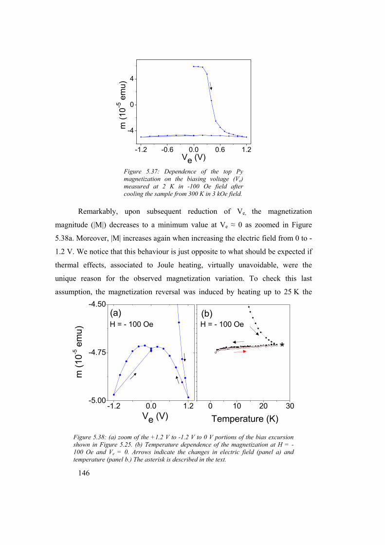
146
-1.2 -0.6 0.0 0.6 1.2
-4
0
4
m
(10-5
em
u)
Ve (V) Figure 5.37: Dependence of the top Py magnetization on the biasing voltage (Ve) measured at 2 K in -100 Oe field after cooling the sample from 300 K in 3 kOe field.
-1.2 0.0 1.2-5.00
-4.75
-4.50
0 10 20 30
m (1
0-5 e
mu)
Ve (V)
(a)H = - 100 Oe H = - 100 Oe
(b)
Temperature (K)
*
Figure 5.38: (a) zoom of the +1.2 V to -1.2 V to 0 V portions of the bias excursion shown in Figure 5.25. (b) Temperature dependence of the magnetization at H = -100 Oe and Ve = 0. Arrows indicate the changes in electric field (panel a) and temperature (panel b.) The asterisk is described in the text.
Remarkably, upon subsequent reduction of Ve, the magnetization
magnitude (|M|) decreases to a minimum value at Ve ≈ 0 as zoomed in Figure
5.38a. Moreover, |M| increases again when increasing the electric field from 0 to -
1.2 V. We notice that this behaviour is just opposite to what should be expected if
thermal effects, associated to Joule heating, virtually unavoidable, were the
unique reason for the observed magnetization variation. To check this last
assumption, the magnetization reversal was induced by heating up to 25 K the

147
0 120 240 360
20.35
20.36
20.37
Ve = 1.8 V (b)
R(Ω
)
θa (deg)
20.69
20.70
20.71
Ve = 0.05V (a)
R (Ω
)
1
2
Figure 5.39: Angular dependence of the magnetoresistance of the Py film when biasing at Ve = 0.05V (panel a, curve 1), 1.8V (panel b) and back to 0.05V (panel a, curve 2).
UL-B sample biased by H = - 100 Oe after FC (3 kOe, from 100 K). As suggested
by data in Figure 5.32b, the exchange bias gradually vanishes as temperature
increases and thus the magnetization should switch from M > 0 to M < 0. Once at
25 K, the magnetization is reversed as signalled by an asterisk in Figure 5.38b.
Then, keeping the sample at H = - 100 Oe, the temperature of the system was
gradually reduced mimicking the role of a decrease of dissipated Joule power
when the electrical bias is reduced. As shown by the data in Figure 5.38a, |M| was
reduced when reducing the electrical bias in manifest contrast to the steady
increase of the magnetization observed when reducing the system temperature
(Figure 5.38a). Note that both panels are in the same vertical scale. Thus, the
electric field effects observed can not be reproduced by simple heating-cooling
effects.
On the basis of the ferroelectric-antiferromagnetic domain wall clamping
reported by Fiebig et al. [Fie02], the previous observations could be connected to
changes in the ferroelectric domain structure. Following that assumption, any
electric-field effect on the Py magnetization induced by changes in the domain
wall structure should be permanent unless the domain structure is modified. To
investigate this point, the reversibility of the AMR cycles upon switching the
electric field was investigated. The data recorded at zero biasing-voltage, after

148
measuring under certain Ve bias-field, were found to be different from the virgin
curves, measured just after FC from 100 K. To illustrate this effect, Figure 5.39
shows, the clockwise R (θa) curves measured sequentially at Ve = 0.05, 1.8 and
0.05 V. From the comparison of the initial and final curves, it is clear that the
exchange bias-field has changed irreversibly upon application of the electric-
biasing field and rotation of the sample. Indeed, the minimum of the R(θa) curves
clearly appears shifted. More precisely, within the accuracy of the model used to
fit the data the exchange bias field has not changed in magnitude but it has rotated
some 60 º from its initial position, all happening at 50 Oe with no other FC
procedure.
In summary, genuine electric field effects on the exchange bias in Py/h-
YMO have been presented in this section. The suppression of magnetic exchange
bias by electric poling of the underlying YMO ferroelectric layer indicates a
substantial modification of the antiferromagnetic domain structure which is driven
by the electric field. The microscopic origin of this effect can not be conclusively
inferred from the present experiments. Beyond the simple exchange bias model
exposed in Chapter 2, it has also been proposed that exchange-bias in
compensated interfaces could be controlled by domain-wall formation and
pinning [Mal88, Now01, Sue03]. This suggestion together with the observation
that AF domains in h-YMO are clamped to the ferroelectric domain walls [Fie02]
and that AF domain walls can extend up to 103 unit cells [Gol03], provides a
framework to understand the observed effects: pinning and/or creation of
antiferromagnetic domain walls at the position of the ferroelectric domain walls
and contributing also to the exchange-bias. Washing out the ferroelectric domains
by applying sufficiently high electric field would result in reducing or rotating of
the exchange bias and a weak dependence on polarity.
5.3.2 Pulsed electric field effects on the exchange bias
Although electric-field induced effects on the exchange bias have been
demonstrated, Joule dissipation is unavoidably present thus combining the effects
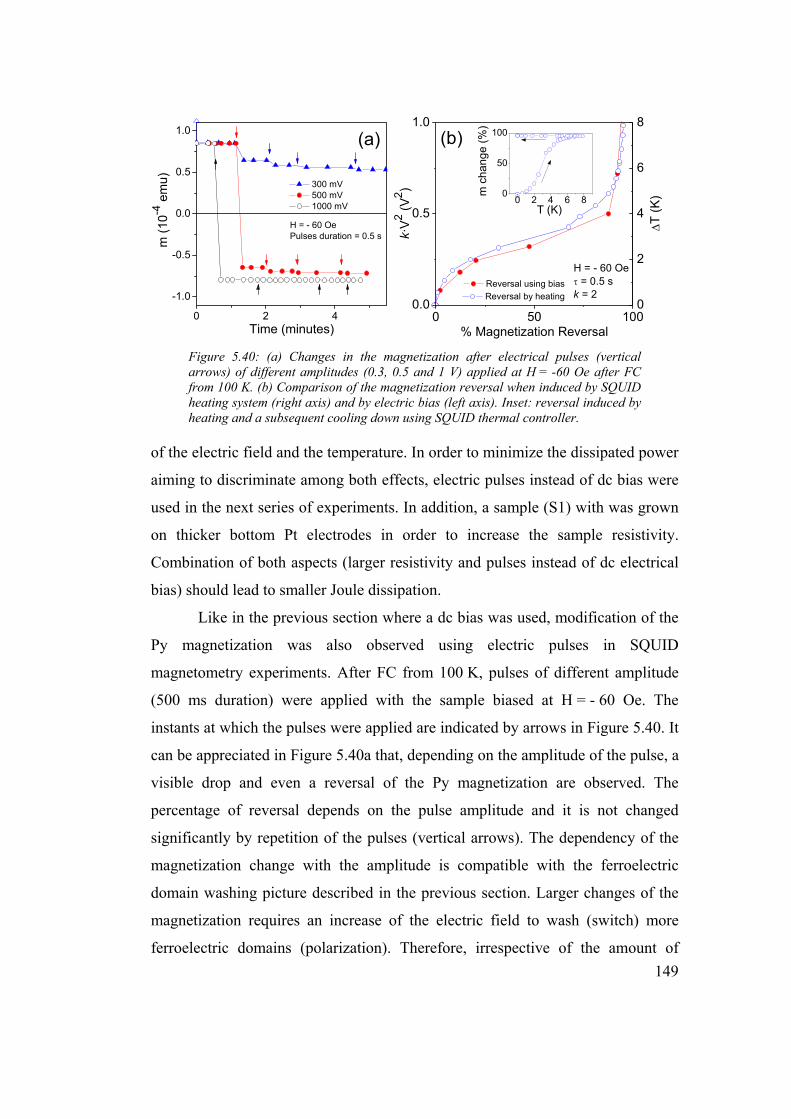
149
0 2 4
-1.0
-0.5
0.0
0.5
1.0
m (1
0-4 e
mu)
(a)
300 mV 500 mV 1000 mV
Time (minutes)
H = - 60 OePulses duration = 0.5 s
0 50 1000.0
0.5
1.0
0
2
4
6
8
0 2 4 6 80
50
100
Reversal using bias
k·V2 (V
2 )
% Magnetization Reversal
H = - 60 Oeτ = 0.5 sk = 2
(b)
Reversal by heating
ΔT
(K)
T (K)
m c
hang
e (%
)
Figure 5.40: (a) Changes in the magnetization after electrical pulses (vertical arrows) of different amplitudes (0.3, 0.5 and 1 V) applied at H = -60 Oe after FC from 100 K. (b) Comparison of the magnetization reversal when induced by SQUID heating system (right axis) and by electric bias (left axis). Inset: reversal induced by heating and a subsequent cooling down using SQUID thermal controller.
of the electric field and the temperature. In order to minimize the dissipated power
aiming to discriminate among both effects, electric pulses instead of dc bias were
used in the next series of experiments. In addition, a sample (S1) with was grown
on thicker bottom Pt electrodes in order to increase the sample resistivity.
Combination of both aspects (larger resistivity and pulses instead of dc electrical
bias) should lead to smaller Joule dissipation.
Like in the previous section where a dc bias was used, modification of the
Py magnetization was also observed using electric pulses in SQUID
magnetometry experiments. After FC from 100 K, pulses of different amplitude
(500 ms duration) were applied with the sample biased at H = - 60 Oe. The
instants at which the pulses were applied are indicated by arrows in Figure 5.40. It
can be appreciated in Figure 5.40a that, depending on the amplitude of the pulse, a
visible drop and even a reversal of the Py magnetization are observed. The
percentage of reversal depends on the pulse amplitude and it is not changed
significantly by repetition of the pulses (vertical arrows). The dependency of the
magnetization change with the amplitude is compatible with the ferroelectric
domain washing picture described in the previous section. Larger changes of the
magnetization requires an increase of the electric field to wash (switch) more
ferroelectric domains (polarization). Therefore, irrespective of the amount of

150
pulses, if the electric field is not increased, the magnetization of the Py should
remain constant.
Now follows a discussion on the possible effects of the heating of the
sample due to Joule dissipation. On one hand, upon the application of the electric
pulses, the thermometers placed in the SQUID did not report any change in the
system temperature. However, owing to the nanometric thickness of the films, it
cannot be concluded, on solid experimental grounds, that the temperature
remained fixed at the nominal temperature of the experiments (i.e. 2 K). It must
be taken into account that the sample is within a thermal bath and that the
thermometers, placed away from the sample, do not detect the local changes of
temperature. On the other hand, a heating-cooling process of the sample might
occur as follows: the electric pulse may produce a sudden heating of the sample
which, if occurs fast enough, could be considered adiabatic. As a result, the
exchange bias would be reduced due to the temperature increase and followed by
a drop of the Py magnetization according to the maximum temperature reached as
shown in Figure 5.32b. Afterwards, there would be a slower (thus allowing heat
exchange with the thermal bath) cooling down back to 2 K while M would be kept
constant. This evolution of the Py magnetization is shown in Figure 5.40b (inset)
using SQUID thermal controls to change the temperature. Note that magnetization
reversal is achieved only by heating the sample up to 8 K and cooling back.
In the main panel of Figure 5.40b is shown the % of magnetization
reversal as a function of the temperature increment ΔT = (Tfinal – 2 K) (right
vertical axis) and k·V2 (left vertical axis). V is the amplitude of each pulse and k is
a constant used to scale the left axis for the purpose of a clearer representation of
the data. Remarkably, the shape of the magnetization reversal curve as a function
of the induced temperature change or the square of the amplitude of the pulse
displayed in the main panel of Figure 5.40b are very similar.
Qualitatively, assuming that the Joule dissipation is proportional to V2 and
that all this energy is absorbed by the sample inducing a change in temperature
proportional to the absorbed energy; data in Figure 5.40b would be compatible
with a magnetization reversal driven by heating effects. However, quantitative

151
estimation of the change in temperature using reported values for heat capacity
and Debye temperature for h-YMO from Ref. [Zho06c] and assuming a adiabatic
heating of the sample leads to unphysical large values. From experimental data in
Ref. [Zho06c], the low temperature specific heat capacity of h-YMO can be fitted
as:
Cp(T) = 1.8 · 10-4 J/mol·K4·T3 Eq. 5.2
The molecular mass of h-YMO is 191 g/mol and the mass of the h-YMO
layer is m = 3·10-6 g (which arises from the volume 6 mm2 (considering only the
Py coated area) times 90 nm thick film and the density of 5.13 g/cm3). The
electric resistance between the top Py layer to the bottom Pt is around 140 Ω (note
that the contact area is 6 mm2). Therefore, the pulses of 0.3 V amplitude and 0.5 s
duration dissipate 0.32 mJ each.
Then, assuming that all energy dissipated in the pulses is absorbed by the
h-YMO film, it follows that
m·Cp(T)·dT = dU Eq. 5.3
Using the Cp(T) shown in Eq. 5.2 in Eq. 5.3 it follows
1.8·10-4 · T3·dT = dU / m Eq. 5.4
Integrating Eq. 5.4 from T = 2 K to T = Tf, it is found:
( ) Km
dUT f 40108.1
4444 =⎟⎟
⎠
⎞⎜⎜⎝
⎛⋅⋅
+⋅=−
Eq. 5.4
Focussing back the attention to Figure 5.40a it turns out that the pulse of
0.3 V (0.5 s) did reverse the magnetization by 10%. If the eventual heating
process due to Joule dissipation was adiabatic, Eq. 5.4 would predict a final
temperature (40 K) well above the total magnetization reversal temperature (8 K)
as seen in Figure 5.40b (right axis). Therefore, data show that if the magnetization
changes were induced by Joule heating, it would not be adiabatic. Indeed, instead

152
of heating up to 40 K, according to Figure 5.40b (right axis), the temperature of
the sample would have been increased only up to 4 K thus indicating that the
thermal bath of 2 K would be absorbing a significant part of the Joule dissipated
energy. However, present experiments do not allow ruling out the possible heating
up to 4 K.
In summary, it turns out that the Joule heating effects cannot be discarded
from the present experiments. Samples with larger resistivity are required to
discard the heating effects. One of the important open issues is why the electric
resistivity measured with contacts as small as 0.2 mm2 is 2 orders of magnitude
larger than with the Py coating of 6 mm2. This issue was early attributed to the
low quality of the h-YMO surface (presenting a high density of h-YMO
nanocrystals). Recent work conducted in collaboration with other members of the
group [Bac09] pointed out that the quality can be dramatically improved by using
thicker Pt layers. In the latest experiments showed in this section, 100 nm thick Pt
were used, but data show that heating effects can not be ruled out by at the present
time and optimization must continue. To progress in this direction, the use of
single crystals of hexagonal YMnO3 coated with permalloy is planned. It would
represent a strategy to circumvent the leakage problem and to investigate the
electric control of the exchange bias.
5.4 Summary of this chapter
Epitaxial Pt(111) electrodes were grown on STO(111) and ALO(0001)
substrates. Laue oscillations were observed around Pt(111) denoting high crystal
quality and smooth surfaces. Films displayed a gradual relaxation with thickness.
In all cases Pt formed two in-plane crystal domains, 180 º in-plane rotated.
Epitaxial relationships were found to be [112]Pt(111) // [1010]ALO(0001) and
[112]Pt(111) // [112]STO(111). Surface morphology was of 2D multilayered
islands. RMS roughness was below 1 nm and presented an increasing trend with
increasing thickness and decreasing temperature.
Epitaxial h-YMO(0001) thin films were grown on top of Pt(111) buffered

153
STO(111) and ALO(0001) substrates. It is found that the thickness of the bottom
Pt electrode must be larger than 3.6 nm to obtain single phase hexagonal films.
Films grown on thinner Pt buffers presented traces of the orthorhombic phase.
Epitaxial (0001)-oriented hexagonal films are obtained on Pt/STO and Pt/ALO at
the 700 – 800 ºC range of substrate temperatures. At lower growth temperatures,
no textured material is found. XRD analysis could not detect differences due to
the changes in PO2. Pole figures and ϕ-scans indicated the relationship: [1100]h-
YMO(0001) // [110]Pt(111). TEM images revealed sharp interfaces. The atomic
stacking of the (0001) planes was resolved by HRTEM. AFM revealed the
presence of nanocrystals with increasing size and number as thickness of the Pt
layer decreased.
Resistivity did not present a systematic dependency with the growth
conditions (PO2 and temperature) of the h-YMO layer. A critical dependence with
the bottom Pt layer thickness is found: compared to an h-YMO film grown on 20
nm thick Pt buffer, more than 2 orders of magnitude larger resistivity is found for
a film grown on 100 nm thick Pt buffer.
Py/h-YMO exchange bias was detected via Squid magnetometry and
AMR. The detection of exchange bias by magnetometry is constrained to
temperatures below 10 K, whereas exchange bias effects were visible in the AMR
set-up at least until 50 K.
Electric field effects did induce changes in the exchange bias and, thus, the
Py magnetization. They were demonstrated using dc and pulsed electrical bias.
Although the Joule dissipation is unavoidable due to the current leakage, there
were signatures of genuine modification exchange bias by electric field which
could not be explained by heating effects.

155
6. General conclusions of the thesis
The present thesis was devoted to the investigation of the growth and
functional properties of thin films of the magnetoelectric YMnO3. As it has been
mentioned in the introduction, YMnO3 can be stabilized as epitaxial thin film in
either the orthorhombic or the hexagonal phases. Since the origin of the
magnetoelectric coupling in each phase is different, so have been the approaches
to investigate each phase and, thus, the thesis has been structured in two separated
blocks. Now are presented the main results and future prospects for each phase.
6.1 Disclosing the origin of ferromagnetism in orthorhombic YMnO3 thin films.
6.1.1 Structural characterization of the films
Epitaxial orthorhombic YMnO3 thin films have been grown on (001)-
oriented SrTiO3 substrates by pulsed laser deposition. The films are (001) oriented
and presented two equivalent crystal domains, 90 º in-plane rotated. These crystal
domains were found to present the following epitaxial relationships: [100]film //
[110]susbtrate and [010]film // [110]susbtrate.
Epitaxial strain was found to be anisotropic: whereas the [100] direction
remains fully relaxed, the [010] direction is contracted and the [001] elongated.
By four different methods the strain in the samples has been
controlled. The unit cell volume was selected as the parameter to summarize the
total unit cell distortion. A set of samples with a smooth variation of unit cell

156
volume down to 97 % of bulk value were produced by
1) Change the oxygen pressure during deposition
2) Different sample thickness
3) 5% substitution of Mn by Co atoms
4) Annealings of strained samples.
6.1.2 Magnetic characterization
Most relaxed YMnO3 films present a pure antiferromagnetic behaviour. As
the unit cell distortion increased, ferromagnetism and a dramatic increase of
susceptibility are observed. The increase in the magnetic response is irrespective
of the four methods how the strain is induced and controlled.
The annealings of YMnO3 samples reveals that oxygen vacancies are not
the cause of the observed weak-ferromagnetism due to the double exchange
interactions in mixed Mn3+/Mn4+. XPS analysis and susceptibility at the
paramagnetic regime indicate that the oxidation state of Mn is 3+.
Atomic force microscopy shows that surface RMS roughness and grain
density are smaller in the more ferromagnetic films. Then, the spin disorder at
surfaces and interfaces are not be the major cause of the ferromagnetism.
Investigation of the magnetic anisotropy supports that the magnetic
response can be understood as an extra ferromagnetic component superimposed to
the pristine antiferromagnetic behaviour and always perpendicular to the [010]
direction, that is, the antiferromagnetic axis. Therefore, the ferromagnetism is
caused by a canting of the antiferromagnetic structure.
Films of the similar orthorhombic TbMnO3 have been investigated
following the same methodology as in o-YMO films. Results indicate that in
TbMnO3 films, correlations of the epitaxial strain and the ferromagnetism are the
same.
It is concluded that ferromagnetism in orthorhombic RMnO3 thin
films is caused by a strain-driven canting of the spins away from the b axis.
157
6.1.3 Magnetoelectric characterization
Dielectric anomalies and magnetoelectric coupling have been observed in
orthorhombic YMnO3 thin films. Both properties can be controlled by the
epitaxial strain.
6.1.4 Next steps
Magnetoelectric measurements with strained single domain o-YMO and o-
TMO films constitute the current work in progress. On the other hand,
measurements of the epitaxial strain and magnetic properties in this thesis are
macroscopic. To progress in the understanding of the magnetoelectric coupling by
epitaxial strain, a mapping of the strain and magnetic properties using synchrotron
techniques would be necessary. This objective constitutes the main goal of the
postdoctoral period.
6.2 Electric field effects using hexagonal YMnO3 thin films
6.2.1 Structural characterization of the heterostructure
Epitaxial Pt(111) bottom electrodes have been grown on SrTiO3(111) and
Al2O3(0001) substrates by sputtering. The epitaxial relationships are
[112]Pt(111) // [1010]Al2O3(0001) and [112]Pt(111) // [112]SrTiO3(111) plus a
180 º in-plane rotated crystal domain on both substrates. Atomic force microscopy
reveals a surface morphology of multilayered islands, with increasing roughness
with increasing temperature deposition and smaller thickness.
Epitaxial YMnO3(0001) films have been grown on Pt(111) buffered
substrates. Thickness of the bottom Pt electrode is found to be critical to grow
single phase hexagonal films with no traces of the orthorhombic phase. Growth
temperatures larger than 700 ºC are required for the (0001) textured growth. The
epitaxial relationship is [1100]YMnO3(0001) // [110]Pt(111). Reciprocal space
maps indicate that the Pt layer is relaxed while the h-YMO film is almost fully
relaxed.

158
Atomic force microscopy reveals that the mound-like morphology from
the underlying Pt electrode is preserved although that there are notable crystalline
outgrowths with number and dimensions increased with decreasing Pt thickness.
Transmission electron microscopy reveals sharp interfaces and a defect-
free stacking of the (0001) planes in YMnO3. It also confirms the epitaxial
relationships obtained by XRD.
6.2.2 Sample resistivity
Sample resistivity is found to be independent of the deposition conditions
but critically dependant on the thickness of the Pt layer. Three orders of
magnitude lower leakage current is measured if the Pt thickness increases from 25
to 100 nm.
Resistivity is found to depend on the size of the contacts, being larger for
smaller contacts. This is attributed to the presence of crystallites at the surface.
6.2.3 Exchange bias characterization
Selected samples have been coated with 15 nm of permalloy.
Magnetometry reveals the presence of exchange bias irrespective of the bottom Pt
thickness. Remarkably, samples prepared in different laboratories presented
similar exchange bias.
Although when measured in SQUID geometry exchange bias is vanished
at 10 K, by angular dependence magnetoresistance exchange bias is still well
visible at 50 K. The difference is attributed to the low in-plane anisotropy of
(0001) surface of YMnO3.
6.2.4 Electric field effects
Modification of the magnetization of the top ferromagnetic permalloy
was achieved by electric pulses and dc biasing of the YMnO3 layer.
Application of electric field reduces the exchange bias. It has been
proposed that the washing of ferroelectric domains in each poling drags the

159
antiferromagnetic domain walls as well thus reducing the exchange bias.
An observed decrease of magnetization when decreasing the electrical
field and the irreversibility of the magnetoresistance loops (with even a rotation of
60 º of the exchange bias axis) after biasing the sample are signatures of a genuine
electric field effect on the exchange bias that cannot be explained by thermal
effects.
6.2.5 Next steps
Next step to take is to reduce the high leakage current in hexagonal
RMnO3 thin films. Due to this, the development of the materials and the bottom
electrodes must continue. Additionally, due to the relevance of the contact size on
the leakage, the use of micrometric size permalloy contacts could be investigated.
On the other hand, the use of single crystals of hexagonal YMnO3 coated
with permalloy would represent an strategy to circumvent the leakage problem to
investigate the electric control of the exchange bias. Imaging of the domain
structure using X-ray absorption holography is planned for the postdoctoral
period.


161
7. References
[Ade08] U. Adem, M. Mostovoy, N. Bellido, A.A. Nugroho, Ch. Simon, and
T.T.M. Palstra, http://arxiv.org/abs/0811.4547
[Alp98] S.P. Alpay, A.S. Prakash, S. Aggarwal, P. Shuk, M. Greenblatt, R.
Ramesh, and A.L. Roytburd, Scr. Mater. 39, 1435 (1998)
[Ake00] B.B.V. Aken, A. Meetsma, T.T.M. Palstra, Acta Cryst. C57, 230 (2001)
[Ake01] B.B.V. Aken, J.-W. G. Bos, R.A. de Groot, and T.T.M. Palstra, Phys.
Rev. B 63, 125127 (2001)
[Ake04] B.B.V. Aken, T.T.M. Palstra, A. Filippetti, and N.A. Spalding, Nature
Mater. 3, 164 (2004)
[Alo00] J.A. Alonso, M.J. Martínez-Lope, M.T. Casais, M.T. Fernández-Díaz,
Inorg. Chem. 39, 917 (2000)
[Alo97] J.A. Alonso, M.J. Martínez-Lope, M.T. Casais, A. Muñoz, Solid State
Comm. 102, 7 (1997) and the reference therein: J.B.A.A. Elemans, B. Van
Laar, K.R. Van der Veen, and B.O. Loopstra, Solid. State Chem. 3, 238 (1971)
[Ast60] D.N. Astrov, Zh. Eksp. Teor. Fiz. 38, 984–985 (1960); Sov. Phys. JETP
11, 708–709 (1960); as cited in Nature Mater. 6, 1 (2007)
[Ast03] A. Asthagiri, C. Niederberger, A.J. Francis, L.M. Poter, P.A. Salvador,
D.S. Sholl, Surf. Sci. 537, 134 (2003)
[Ats96] T. Atsumi, T. Ohgushi, N. Kamegashira, J. Alloys Comp. 238, 35 (1996)
[Bac09] R. Bachelet, R. Muralidharan, F. Rigato, N. Dix, X. Marti, J. Santiso, F.
Sánchez, and J. Fontcuberta, Appl. Phys. Lett, in press
[Bal06] K.R. Balasubramanian, K. Chang, A.F. Mohammad, L.M. Porter, P.A.

162
Salvador, J. DiMaio, R. Davis, Thin Solid Films 515, 1807 (2006)
[Ber08] R. Bertacco, A. Tagliaferri, M. Riva, L. Signorini, M. Cantón, A. Cattoni,
and F. Cicacci, Phys. Rev. B 78, 035448 (2008)
[Bey06] E. Beyreuther, S. Grafstrom, L.M. Eng, C. Thiele, and K. Dörr, Phys.
Rev. B 73, 155425 (2006)
[Bla06] M.G. Balmire and B. Hickey, Nature Mater. 5, 87 (2006)
[Bor05] P. Borisov, A. Hochstrat, X. Chen, W. Kleemann, and C. Binek, Phys.
Rev. Lett. 94, 117203 (2005)
[Bos01] A.A. Bosak, A.A. Kamenev, I.E. Graboy, S.V. Antonov, O.Yu.
Gorbenko, A.R. Kaul, C. Dubourdieu, J. P. Senateur, V.L. Svechnikov, H.W.
Zandbergenc and B.Holländerd, Thin Solid Films 400, 149 (2001)
[Bri97] H.W. Brinks, H. Fjellvag, and A. Kjekshus, J. Sol. Sta. Chem. 129, 334
(1997)
[Bro06] P.J. Brown and T. Chatterji, J. Phys. Cond. Matter. 18, 10085 (2006)
[Che07] S.-W. Cheong and M. Mostovoy, Nature Mater. 6, 13 (2007)
[Che07b] Y. Chen, H. Yuan, G. Li, G. Tian, and S. Feng, J. Cryst. Growth 305,
242 (2007)
[Cur94] P. Curie, J. Phys. 3(Ser. III), 393–415 (1894); as cited in Nature Mater. 6,
1 (2007)
[Cul78] B.D. Cullity, Elements of X-ray diffraction, 2nd edition, Addison-Wesley
Publishing Company Inc. (1978)
[Dau09] C.J.M. Daumont, D. Mannix, S. Venkatessan, G. Catalan, D. Rubi, B.J.
Kooi, J.Th.M. De Hosson, and B. Noheda, J. Phys. Condens. Matter. 21,
182001 (2009)
[Dau09b] C. Daumont, PhD thesis, Zernike Institute for Advanced Materials,
University of Groningen, 2009
[Dho04] J. Dho, C.W. Leung, J.L. MacManus-Driscoll, M.G. Blamire, J. Crys.
Growth 267, 548 (2004)
[Dho05] J. Dho and M.G. Blamire, Appl. Phys. Lett. 87, 252504 (2005)
[Duc03] J.R. Duclère, M. Gilloux-Viry, V. Bouquet, A. Perrin, E. Cattan, C.
Soyer, and D. Rèmiens, Appl. Phys. Lett. 83, 5500 (2003)
163
[Dzy59] I.E. Dzyaloshinskii, Zh. Eksp. Teor. Fiz. 37, 881–882 (1959); Sov. Phys.
JETP 10, 628–629 (1959); as cited in Nature Mater. 6, 1 (2007)
[Edw51] J.W. Edwards, R. Speiser, H.L. Johnston, J. Appl. Phys. 22, 424 (1951)
[Eer06] W. Eerenstein, N.D. Mathur, and J.F. Scott, Nature 422, 759 (2006)
[Esk08] K. Uusi-Esko, J. Malm, N. Imamura, H. Yamauchi, and M. Karppinen,
Mater. Chem. Phys. 112, 1029 (2008)
[Fab08] X. Fabrèges, I. Mirebeau, P. Bonville, S. Petit, G. Lebras-Jasmin, A.
Forget, G. André, and S. Pailhès, Phys. Rev. B 78, 214422 (2008)
[Far93] R.F.C. Farrow, G.R. Harp, R.F. Marks, T.A. Rabedeau, M.F. Toney, and
D. Weller, J. Crys. Growth 133, 45-58 (1993)
[Fie00] M. Fiebig, D. Fröhlich, K. Kohn, St. Leute, Th. Lottermoser, V. V.
Pavlov, and R.V. Pisarev, Phys. Rev. Lett. 84, 5620 (2000)
[Fie02] M. Fiebig, Th. Lottermoser, D. Fröhlich, A. V. Goltsev, and R.V.
Pisarev, Nature 419, 818 (2002)
[Fie03] M. Fiebig, Th. Lottermoser, and R.V. Pisarev, J. Appl. Phys. 93, (2003)
[Fie05] M. Fiebig, J. Phys. D: Appl. Phys. 38, R123 (2005)
[Fre66] H.P.R. Frederiske and G.A. Candela, Phys. Rev. 147, 2 (1966)
[Fuj96a] N. Fujimura, T. Ishida, T. Yoshimura, T. Ito, Appl. Phys. Lett. 69, 1011
(1996)
[Fuj96b] N. Fujimura, S. Azuma, N. Aoki, T. Yoshimura, and T. Ito, J. Appl.
Phys. 80, 7084 (1996)
[Fuj03] N. Fujimura, H. Sakata, D. Ito, T. Yokota and T. Ito, J. Appl. Phys. 93,
6990 (2003)
[Fuj07] N. Fujimura, N. Shigemitsu, T. Takahashi, A. Ashida, T. Yoshimura, H.
Fukura, H. Arima, Phil. Mag. Lett. 87, 193 (2007)
[Gaj07] M. Gajek, M. Bibes, S. Fusil, K. Bouzehouane, J. Fontcuberta, A.
Barthélémy, and A. Fert, Nature Mater. 6, 296 (2007)
[Gal02] V. R. Galakhov, M. Demeter, S. Bartkowski, M. Neumann, N.A.
Ovechkina, E.Z. Kurmaev, N. I. Lobachevskaya, Ya. M. Mukovskii, J.
Mitchell, D.L. Ederer, Phys. Rev. B 65, 113102 (2002)
[Gel08] I. Gellard, C. Dubourdieu, S. Pailhès, S. Petit, and Ch. Simon, Appl.

164
Phys. Lett. 92, 232506 (2008)
[Gel09] I. Gellard, PhD thesis, Institut Polytechnique de Grenoble, 2009
[Gic07] M. Gich, C. Frontera, A. Roig, J. Fontcuberta, E. Molins, N. Bellido, Ch.
Simon and C. Fleta, Nanotechn. 17, 687 (2006)
[Gill99] B. Gillot, S. Buguet, E. Kester, C. Baubet, and P. Tailhades, Thin Solid
Films 357, 223 (1999)
[Gol03] A.V. Goltsev, R.V. Pisarev, Th. Lottermoser, and M. Fiebig, Phys. Rev.
Lett. 90, 177204 (2003)
[Goo63] J.B. Goodenough, Magnetism and the chemical bond, John Wiley and
Sons (1963)
[Gor02] O.Y. Gorbenko, S.V. Samoilenkov, I.E. Graboy, and A.R. Kaul, Chem.
Mater 14, 4026 (2002)
[Gra03] I.E. Graboy, A.A. Bosak, O.Y. Gorbenko, A.R. Kaul, C. Dubornieu, J.P.
Sénateur, V.L. Svetchnikov, H.W. Zandbergen, Chem. Mater. 15, 2632 (2003)
[Hem07] J. Hemberger, F. Schrettle, A. Pimenov, P. Lunkenheimer, V.Yu.
Ivanov, A.A. Mukhin, A.M. Balbashov, and A. Loidl, Phys. Rev. B 75, 035118
(2007)
[Hill00] N.A. Hill, J. Phys. Chem. B 104, 6694 (2000)
[Hill02] N.A. Hill, J. Phys. Chem. B 104, 6694 (2000); N.A. Hill, A. Filipetti, J.
Magn. Magn. Mater. 242-245, 976 (2002)
[Hof04] A. Hoffmann, Phys. Rev. Lett. 93, 097203 (2004)
[Hsi08] C.C. Hsieh, T.H. Lin, H.C. Shih, C.-H. Shu, C.W. Luo, L.-Y. Lin, K.H.
Wu, T.M. Uen, J.Y. Juang, J. Appl. Phys 104, 103902 (2008); C.C. Hsieh, T.H.
Lin, H.C. Shih, J.-Y. Lin, C.-H. Hsu, C.W. Luo, K.H. Wu, T.M. Uen and J.Y.
Juang, J. Phys.: Conf. Ser. 150, 042062 (2009)
[Hua97] Z. J. Huang, Y. Cao, Y.Y. Sun, Y.Y. Xue, and C.W. Chu, Phys. Rev. B
56, 2623 (1997)
[Hua06] Y.H. Huang, H. Fjellvåg, M. Karppinen, B.C. Hauback, H. Yamauchi,
and J.B. Goodenough, Chem. Mater. 18, 2130 (2006)
[Hur04] N. Hur, S. Park, P.A. Sharma, J.S. Ahn, S.Guha, and S-W. Cheong,
Nature 429, 392 (2004)

165
[Ili98] M.N. Iliev, M.V. Abrashev, H.G. Lee, V.N. Popov, Y.Y. Sun, C. Thomsen,
R.L. Meng, C.W. Chu, Phys. Rev. B 57, 2872 (1998)
[Ili05] M.N. liev, B. Lorenz, A.P. Litvinchuk, Y.Q. Wang, Y.Y. Sun, C.W. Chu,
J. Phys. Condens. Matter 17, 3333 (2005)
[Iva06] V.Y. Ivanov, A.A. Mukhin, A.S. Prokhorov, A.M. Balbashov, and L.D.
Iskhakova, Phys. Solid State 48, 1726 (2006)
[Ish97] S. Ishihara, J. Inoue, and S. Maekawa, Phys. Rev. B 55, 8280 (1997)
[Ito03a] D. Ito, N. Fujimura, T. Yoshimura, and T. Ito, J. Appl. Phys. 93, 5563
(2003)
[Ito03b] D. Ito, N. Fujimura, T. Yoshimura, and T. Ito, J. Appl. Phys. 94, 4036
(2003)
[Jen74] G.B Jensen and O.V. Nielsen, J. Phys. C: Solid State Phys. 7, 409 (1974)
[Jeo07] I.-K. Jeong, N. Hur, and Th. Proffen, J. Appl. Cryst. 40, 730 (2007)
[Jes69] W.A. Jesser, Mater. Sci. Eng. 4, 279 (1969)
[Jir85] Z. Jirák, S. Krupička, Z. Šimša, M. Dlouhá and S. Vratislav, J. Magn.
Magn. Mater. 53, 153 (1985)
[Kaj04] R. Kajimoto, H. Yoshizawa, H. Shintani, T. Kimura, and Y. Tokura,
Phys. Rev. B 70 012401 (2004)
[Kau04] A.R. Kaul, O.Y. Gorbenko and A.A. Kamenev, Russ. Chem. Rev. 73,
861 (2004)
[Kat01] T. Katsufuji, S. Mori, M. Masaki, Y. Moritomo, N. Yamamoto, H.
Takahagi, Phys. Rev. B 64, 104419 (2001)
[Kat02] T. Katsufuji, M. Masaki, A. Machida, M. Morimoto, K. Kato, E.
Nishibori, M. Takata, M. Sakata, K. Ohoyama, K. Kitzawa, and H. Takagi,
Phys. Rev. B 66, 134434 (2002)
[Kat05] H. Katsura, N. Nagaosa, and A.V. Balatsky, Phys Rev. Lett. 95, 057205
(2005)
[Ken05] M. Kenzelmann, A.B. Harris, S. Jonas, C. Broholm, J. Schefer, S.B.
Kim, C.L. Zhang, S.-W. Cheong, O.P. Vajk, and J.W. Lynn, Phys. Rev. Lett.
95, 087206 (2005)
[Kho09] D. Khomskii, Physics 2, 20 (2009)

166
[Kim03] T. Kimura, T. Goto, H. Shintani, K. Ishizaka, T. Arima, and Y. Tokura,
Nature 426, 55 (2003)
[Kim03b] T. Kimura, S. Kawamoto, I. Yamada, M. Azuma, M. Takano, and Y.
Tokura, Phys. Rev. B 67, 180401 (2003)
[Kim03c] T. Kimura, S. Ishihara, H. Shintani, T. Arima, K.T. Takahashi, K.
Ishizaka, and Y. Tokura, Phys. Rev. B 68, 060403R (2003)
[Kim04] T. Goto, T. Kimura, G. Lawes, A.P. Ramirez, and Y. Tokura, Phys. Rev.
Lett 92, 257201 (2004)
[Kim05] T. Kimura, G. Lawes, T. Goto, Y. Tokura, and A.P. Ramírez, Phys. Rev.
B 71 224425 (2005)
[Kim07] J.W. Kim, K. Dörr, K. Nenkov, L. Schultz, J. Appl. Phys. 101, 09M108
(2007)
[Kir09] B.J. Kirby, D. Kan, A. Luykx, M. Murakami, D. Kundaliya, and I.
Takeuchi, J. Appl. Phys. 105, 07D917 (2009)
[Kon08] S. Kondo, K. Tateishi, and N. Ishizawa, Jpn. J. Appl. Phys. 47, 616
(2008)
[Kuc06] W. Kuch, L.I. Chelaru, F. Offi, J. Wang, M. Kotsugi, and J. Kirschner,
Nature Mater. 5, 128 (2006)
[Lam00] D.G. Lamas and N.E. Walsoe de Reca, J. Mater. Sci. 35, 5563 (2000)
[Lag02] M.G. Lagally and Z. Zhang, Nature 417, 907 (2002)
[Lee06] S. Lee and J.G. Park, Neutron News 17, 24 (2006)
[Lin09] T.H. Lin, H.C. Shih, C.C. Hsieh, C.W. Luo, J.-Y. Lin, J.L. Her, H.D.
Yang, C.-H. Hsu, K.H. Wu, T.M. Uen, and J.Y. Juang, J. Phys. Condens.
Matter 21, 026013 (2009); T.H. Lin, C.C. Hsieh, H.C. Shih, C.W. Luo, T.M.
Uen, K.H. Wu, J. Y. Juang, J.-Y. Lin, C.-H. Hsu, and S. J. Liu, Appl. Phys.
Lett. 92, 132503 (2008)
[Lit94] S. Little and A. Zangwill, Phys. Rev. B 49, 16659 (1994)
[Lor04] B. Lorenz, Y.Q. Wang, Y.Y. Sun, and C.W. Chu, Phys. Rev. B 70,
212412 (2004)
[Lor04b] B. Lorenz, A.P. Litvinchuk, M.M. Gospodinov, and C.W. Chu, Phys.
Rev. Lett. 92, 087204 (2004)

167
[Lor07] B. Lorenz, Y.-Q. Wang, C.W. Chu, Phys. Rev. B 76, 104405 (2007)
[Lot04] T. Lottermoser, and M. Fiebig, Phys. Rev. B 70, 220407 (2004)
[Mae07] K. Maeda, T. Yoshimura, N. Fujimura, IEEE Trans. Ultrason.,
Ferroelectrics Freq. Control 54, 2641 (2007)
[Mal88] A. P. Malozemoff, J. Appl. Phys. 63, 3874 (1988)
[Mar06a] X. Marti, F. Sánchez, J. Fontcuberta, C. Ferrater, M.V. García-Cuenca,
and M. Varela, J. Appl. Phys. 99, 08P302 (2006)
[Mar06b] X. Marti, F. Sánchez, D. Hravobsky, L. Fabrega, A. Ruyter, J.
Fontcuberta, V. Laukhin, V. Skumryev, M.V. García Cuenca, C. Ferrater, M.
Varela, A. Vilà, U. Lüders, J.F. Bobo, Appl. Phys. Lett. 89, 032510 (2006)
[Mar06c] V. Laukhin, V. Skumryev, X. Marti, D. Hravobsky, F. Sánchez, M.V.
García Cuenca, C. Ferrater, M. Varela, U. Lüders, J.F. Bobo, J. Fontcuberta,
Phys. Rev. Lett. 92, 227201 (2006)
[Mar07] X. Marti, V. Skumryev, V. Laukhin, F. Sánchez, M.V. García-Cuenca,
C. Ferrater, M. Varela, J. Mater. Res. 22, 2096 (2007)
[Mar07b] X. Marti, F. Sánchez, D. Hravobsky, J. Fontcuberta, V. Laukhin, V.
Skumryev, M.V. García Cuenca, C. Ferrater, M. Varela, U. Lüders, J.F. Bobo,
S. Estradé, J. Arbiol, F. Peiró, J. Cryst. Growth 299, 288 (2007)
[Mar07c] V. Laukhin, X. Marti, V. Skumryev, D. Hravobsky, F. Sánchez, M.V.
García Cuenca, C. Ferrater, M. Varela, U. Lüders, J.F. Bobo, J. Fontcuberta,
Philos. Mag. Lett. 87, 183 (2007)
[Mar08] X. Marti, F. Sánchez, V. Skumryev, V. Laukhin, C. Ferrater, M.V.
García-Cuenca, M. Varela, and J. Fontcuberta, Thin Solid Films 516, 4899
(2008)
[Mar09] X. Marti, V. Skumryev, A. Cattoni, R. Bertacco, V. Laukhin, C. Ferrater,
M.V. García-Cuenca, M. Varela, F. Sánchez, and J. Fontcuberta, J. Magn.
Magn. Mat. 321, 1719 (2009)
[Mar09b] X. Marti, I. Fina, V. Skumryev, C. Ferrater, M. Varela, F. Sánchez, and
J. Fontcuberta, Appl. Phys. Lett. 95, 142903 (2009)
[Mat75] J.W. Matthews, J. Vac. Sci. Tecnol. 12, 126 (1975)
[Mei57] W.H. Meiklejohn and C.P. Bean, Phys. Rev. 105, 904 (1957)

168
[Mey81] G.M. Meyer, R.J. Nelmes, and J. Hutton, Acta Cryst. A 37, 916 (1981)
[Mil96] B.H. Miller and D. Dahlberg, Appl. Phys. Lett. 69, 3932 (1996)
[Mor02] A. Moreira dos Santos, S. Parashar, A.R. Raju, Y.S. Zhao, A.K.
Cheetham, and C.N.R. Rao, Solid State Comm. 122, 49 (2002); A. Moreira dos
Santos, A.K. Cheetham, W. Tian, X. Pan, Y. Jia, N.J. Murphy, J. Lettieri, D.G.
Schlom, Appl. Phys. Lett. 84, 91 (2004)
[Mor03] Y. Morimoto, Y. Ohishi, A. Kuriki, E. Nishibori, M. Takata, M. Sakata,
J. Phys. Soc. Jpn. 72, 765 (2003)
[Mor07] N.O. Moreno, J.G.S. Duque, P.G. Pagliuso, C. Rettori, R.R. Urbano, and
T. Kimura, J. Magn. Magn. Mater. 310, e364 (2007)
[Mos06] M. Mostovoy, Phys. Rev. Lett. 96, 067601 (2006)
[Muñ00] A. Muñoz, J.A. Alonso, M.J. Martínez-Lope, M.T. Casais, J.L.
Martínez, M.T. Fernández-Díaz, Phys. Rev. B 62, 9498 (2000)
[Muñ01] A. Muñoz, M.T. Casais, J.A. Alonso, M.J. Martínez-Lope, J.L.
Martínez, M.T. Fernández-Díaz, Inorg. Chem. 40, 1020 (2001)
[Muñ01b] A. Muñoz, J.A. Alonso, M.J. Martínez-Lope, M.T. Casais, J.L.
Martínez, M.T. Fernández-Díaz, Chem. Mater. 13, 1497 (2001)
[Muñ02] A. Muñoz, J.A. Alonso, M.T. Casais, M.J. Martínez-Lope, J.L.
Martínez, M.T. Fernández-Díaz, J. Phys. Condens. Matter 14, 3285 (2002)
[Nen05] G. Nenert, Y. Ren, H.T. Stokes, T.T.M. Palstra,
http://arxiv.org/abs/cond-mat/0504546
[Nog99] J. Nogués, and I.K. Schuller, J. Magn. Magn. Mater. 192, 203 (1999)
[Now01] U. Nowak, A. Misra and K.D. Usadel, J. Appl. Phys. 89, 7269 (2001)
[Nug07] A.A. Nugroho, N. Bellido, U. Adem, G. Nénert, Ch. Simon, M.O. Tija,
M. Mostovoy, and T.T.M Palstra, Phys. Rev. B 75, 174435 (2007)
[Oka08] Lu-; H. Okamoto, N. Imamura, B.C. Hauback, M. Karppinen, H.
Yamauchi and H. Fjellvåg, Solid State Comm. 146, 152 (2008)
[Par54] L.G. Parratt, Phys. Rev. 95, 359 (1954)
[Par02] J. Park, U. Kong, S.I. Choi, J,-G. Park, C. Lee, W. Jo, Appl. Phys A 74,
802 (2002)
[Pom93] W. Pompe, X. Gong, Z. Zuo, and J.S. Speck, J. Appl. Phys. 74, 6012

169
(1993)
[Pre05] W. Prellier, M.P. Singh, and P. Murugavel, J. Phys.: Condens. Matter 17,
R803 (2005)
[Rad07] F. Radu, and H. Zabe, http://arxiv.org/abs/0705.2055
[Ram07] R. Ramesh and N.A. Spalding, Natutre Mater. 6, 21 (2007)
[Rok00] E. Rokuta, Y. Hotta, H. Tabata, H. Kobayashi, T. Kawai, J. Appl. Phys.
88, 6598 (2000)
[Roy98] A.L. Roytburd, J. Appl. Phys. 83 (1998) 228
[Rub08] Yb-; D. Rubi, S. Venkatesan, B.J. Kooi, J.Th.M. De Hosson, T.T.M.
Palstra, and B. Noheda, Phys. Rev. B 78, 020408 (2008)
[Rub09] Tb-; D. Rubi, C. de Graaf, C.J.M. Daumont, D. Mannix, R. Broer, and B.
Noheda, Phys. Rev. B 79, 014416 (2009)
[Sal98] P.A. Salvador, T.-D. Doan, B. Mercey, and B. Raveau, Chem. Mater. 10,
2592 (1998)
[San06]: F. Sánchez, I.C. Infante, U. Lüders, Ll. Abad, J. Fontcuberta, Surf. Sci.
600, 1231 (2006)
[Ser06] I.A. Sergienko, C. Sen, E. Dagotto, Phys. Rev. Lett 97, 227204 (2006)
[Sha76] Ionic radius data; R.D. Shannon, Acta Cryst. A32, 751 (1976)
[Shi08] D. Shindo, T. Yoshimura, N. Fujimura, Appl. Surf. Sci. 254, 6218 (2008)
[Sku09] V. Skumryev, M. Kuzmin, M. Gospodinov, and J. Fontcuberta, Phys.
Rev. B. 79, 212414 (2009)
[Str95]: J.A. Stroscio, D.T. Pierce, M.D. Stiles, A. Zangwill, and L.M. Sander,
Phys. Rev. Lett. 75, 4246 (1995)
[Sue03] D. Suess, M. Kirschner, T. Schrefl, J. Fiedler, R.L. Stamps, and J.V. Kim,
Phys. Rev. B 67, 054419 (2003)
[Sug02] H. Sugie, N. Iwata, K. Kohn, J. Phys. Soc. Jap. 71, 1558 (2002)
[Tac07] Tackett, G. Lawes, B. C. Melot, M. Grossman, E. S. Toberer, and R.
Seshadri, Phys. Rev. B 76, 024409 (2007)
[Trt99] V. Trtik, A. Pérez, J. Navarro, C. Ferrater, F. Sánchez, and M. Varela,
Appl. Phys. A 69, S815 (1999)
[Tsa04] F.C. Tsao, P.J. Huang, C.C. Yang, S.Y. Wu, W.H. Li, K.C. Lee, J.W.
170
Lynn, H.C. Cu, J. Magn. Magn. Mater. 272, 1778 (2004)
[Wai67] A. Waintal and C. Chenavas, Mat. Res. Bull. 2, 819 (1967)
[Wan03] J. Wang, J.B. Neaton, H. Zheng, V. Nagarajan, S.B. Ogale, B. Liu, D.
Viehland, V. Vaithyanathan, D.G. Schlom, U.V. Waghmare, N.A. Spaldin,
K.M. Rabe, M. Wuttig, R. Ramesh, Science 299, 1719 (2003)
[Wu00] Nd-; S.Y. Wu, C.M. Kuo, H.Y. Wang, W.-H. Li, K.C. Lee, J.W. Lynn,
and R.S. Liu, J. Appl. Phys. 87, 5822 (2000)
[Yan07] C. Yan, Y. Hongming, L. Guanghua, T. Ge, and F. Shouhua, J. Crys.
Growth 305, 242 (2007)
[Ye07] Er-; F. Ye, B. Lorenz, Q. Huang, Y. Q. Wang, Y. Y. Sun, C. W. Chu, J. A.
Fernandez-Baca, Pengcheng Dai, and H. A. Mook, Phys. Rev. B 76,
060402(R) (2007)
[Yen07] F. Yen, C. dela Cruz, B. Lorenz, E. Galstyan, Y.Y. Sun, J. Mater. Res.
22, 2163 (2007)
[Zav07] F. Zavaliche, T. Zhao, H. Zheng, F. Straub, M. P. Cruz, P.-L. Yang, D.
Hao, and R. Ramesh, Nano Lett. 7, 1586 (2007)
[Zhe04] H. Zheng, J. Wang, S.E. Lofland, Z. Ma, L. Mohaddes-Ardabili, T. Zhao,
L. Salamanca-Riba, S.R. Shinde, S.B. Ogale, F. Bai, D. Viehland, Y. Jia, D.G.
Schlom, M. Wuttig, A. Roytburd, R. Ramesh, Science 303, 661 (2004)
[Zho84] L. Zhong and V. Young, J. Electron Spectr. Rel. Phenom. 34, 45 (1984)
[Zho04] L. Zhou, Y.P. Wang, Z.G. Liu, W.Q. Zou, Y.W. Du, Phys. Stat. Sol. 201,
497 (2004)
[Zho06] J.-S. Zhou, J. B. Goodenough, J.M. Gallardo-Amores, E. Morán, M.A.
Alario-Franco, and R. Caudillo, Phys. Rev. B 74, 014422 (2006)
[Zho06b] J.-S. Zhou, J.B. Goodenough, Phys. Rev. Lett 96, 247202 (2006)
[Zho06c]: H.D. Zhou, J.A. Janik, B.W. Vogt, Y.J. Jo, L. Balicas, M.J. Case, C.R.
Wiebe, J.C. Denyszyn, J.B. Goodenough, J.G. Cheng, Phys. Rev. B 74, 094426
(2006)

171
8. List of publications
1 Exchange bias between magnetoelectric YMnO3 and ferromagnetic
SrRuO3 epitaxial films
X. Marti, F. Sánchez, J. Fontcuberta, M.V. García-Cuenca, C. Ferrater,
M. Varela
Journal of Applied Physics 99, 08P302 (2006)
2 Exchange bias and electrical polarization with YMnO3
X. Marti, F. Sánchez, D. Hravobsky, L. Fabrega, A. Ruyter, J. Fontcuberta,
V. Laukhin, V. Skumryev, M.V. García-Cuenca, C. Ferrater,
M. Varela, A. Vilà, U. Lüders, J.F. Bobo
Applied Physics Letters 89, 032510 (2006)
3 Electric-field control of exchange bias in multiferroic epitaxial
heterostructures
V. Laukhin, V. Skumryev, X. Marti, D. Hravobsky, F. Sánchez,
M.V. García-Cuenca, C. Ferrater, M. Varela, U. Lüders, J.F. Bobo,
J. Fontcuberta
Physical Review Letters 92, 227201 (2006)
Compiled in the Virtual Journal of Nanoscale Science and Technology
4 Epitaxial growth of YMnO3(0001) on platinum electrodes
X. Marti, F. Sánchez, D. Hravobsky, J. Fontcuberta, V. Laukhin,
V. Skumryev, M.V. García-Cuenca, C. Ferrater, M. Varela,
U. Lüders, J.F. Bobo, S. Estradé, J. Arbiol, F. Peiró
Journal of Crystal Growth 299, 288 (2007)

172
5 Electric field effects on magnetotransport properties of multiferroic
Py/YMnO3/Pt heterostructures
V. Laukhin, X. Marti, V. Skumryev, D. Hravobsky, F. Sánchez,
M.V. García-Cuenca, C. Ferrater, M. Varela, U. Lüders, J.F. Bobo,
J. Fontcuberta
Philosophical Magazine Letters 87, 183 (2007)
6 Dielectric anomaly and magnetic response of epitaxial orthorhombic
YMnO3 thin films
X. Marti, V. Skumryev, V. Laukhin, F. Sánchez, M.V. García-Cuenca,
C. Ferrater, M. Varela, J. Fontcuberta
Journal of Materials Research 22, 2096 (2007)
7 Strain-induced stabilization of new magnetic spinel structures in
epitaxial oxide heterostructures
F. Rigato, S. Estradé, J. Arbiol, F. Peiró, U. Lüders, X. Marti, F. Sánchez,
J. Fontcuberta
Materials Science and Engineering B 144, 43 (2007)
8 Crystal texture selection in epitaxies of orthorhombic
antiferromagnetic YMnO3 thin films
X. Marti, F. Sánchez, V. Skumryev, V. Laukhin, C. Ferrater,
M.V. García-Cuenca, M. Varela, J. Fontcuberta
Thin Solid Films 516, 4899 (2008)
9 Ferromagnetism in orthorhombic YMnO3 thin films
X. Marti, V. Skumryev, A. Cattoni, R. Bertacco, V. Laukhin, C. Ferrater,
M.V. García-Cuenca, M. Varela, F. Sánchez, J. Fontcuberta
Journal of Magnetism and Magnetic Materials 321, 1719 (2009)
10 Strain tuned magnetoelectric coupling in orthorhombic YMnO3 thin
films
X. Marti, I. Fina, V. Skumryev, C. Ferrater, M. Varela, L. Fábrega,
F. Sánchez, and J. Fontcuberta
Applied Physics Letters 95, 142903 (2009)
173
11 Enhanced thermal stability of Pt electrodes for flat epitaxial biferroic-
YMnO3/Pt heterostructures
R. Bachelet, R. Muralidharan, F. Rigato, N. Dix, X. Martí, J. Santiso, F.
Sánchez, and J. Fontcuberta
Applied Physics Letters 95, 181907 (2009).
12 Disclosing the origin of ferromagnetism in epitaxial orthorhombic
YMnO3 thin films
X. Marti, V. Skumryev, V. Laukhin, C. Ferrater, M.V. García-Cuenca,
M. Varela, F. Sánchez, J. Fontcuberta
Submitted to Physical Review B
13 Strain-driven ferromagnetism in epitaxial TbMnO3 thin films
X. Marti, V. Skumryev, V. Laukhin, C. Ferrater, M.V. García-Cuenca,
M. Varela, F. Sánchez, J. Fontcuberta
In preparation
8.1 Other scientific contributions
1 Exchange biasing with YMnO3 epitaxial films
J. Fontcuberta, X. Marti, F. Sánchez, D. Hravobsky, V. Laukhin,
V. Skumryev, N. Dix, M.V. García-Cuenca, C. Ferrater, M. Varela,
U. Lüders, J.F. Bobo
Advances in Science in Technology 52, 62 (2006)
Edited by Trans Tech Publications. Proceedings de 11th International
Conferences on Modern Materials and Technologies (CIMTEC 2006).
8.2 Patents
1 Patent P2824PC00 (2006)
“Magnetoelectric device and procedures to write non-volatile information
in such device” developed during my PhD thesis in ICMAB and accepted
in USA.

174
9. List of oral presentations
1 Epitaxial stabilization of orthorhombic YMnO3 thin films
X. Marti, F. Sánchez, J. Fontcuberta, M.V. García-Cuenca, C. Ferrater,
M. Varela
2nd Thin Films Novel Oxide Devices (THIOX) Meeting
Genova (Italy), 17th-18th May 2005
2 Tunable exchange bias with biferroic YMnO3 epitaxial thin films
J. Fontcuberta, X. Marti, F. Sánchez, D. Hravobsky, V. Laukhin,
V. Skumryev, M.V. García-Cuenca, C. Ferrater, M. Varela,
S. Estradé, J. Arbiol, F. Peiró, U. Lüders, J.F. Bobo
13th International Workshop On Oxide Electronics (WOE13)
Ischia (Italy), 8th-11th October 2006
3 Ferromagnetism in epitaxial orthorhombic YMnO3 thin films
X. Marti, V. Skumryev, A. Cattoni, R. Bertacco, V. Laukhin, C. Ferrater,
M.V. García-Cuenca, M. Varela, F. Sánchez, J. Fontcuberta
European School of Multiferroics (ESMF2008)
Girona (Spain), 1st-5th September 2008
4 “X-ray reflectivity thin film analysis” (invited)
X. Marti
Workshop on the applications of X-rays to materials
Bellaterra (Spain), 24th November 2008
As well as these oral contributions presented personally, during the PhD I
presented personally four posters and I am co-author of other 12 oral contributions
presented by other co-authors.

175
Appendix A: angular scale correction in XRD θ/2θ scans
In X-ray diffraction θ/2θ scans, peaks are expected at θ angular positions
according the Bragg’s law:
( ) λθ ·2sin·2 nd =ll Eq. A.1
In the equation d is the interplanar distance perpendicular to the plane, n
the order of diffraction and λ is the wavelength of the incoming X-rays. In the
case of thin films grown on single-crystal substrates, a first crosscheck is to
evaluate if the diffraction peaks contributed by the substrate appear at the
expected positions. Usually, due to unavoidable experimental issues, for instance
the misallocation of the sample in the vertical axis, a small shift in the angular
position appears. Additionally, this shift is usually not constant in all the angular
range scanned.
In the case of textured thin films, the out-of-plane lattice parameter can be
extracted after compensating the misalignment effects. For instance, it can be
performed by computing the angular shift in a substrate peak near the film peak of
interest and assuming that the correction will be constant. Note that if there are
not closer substrate peaks, the angular correction cannot be accurate. Moreover,
since the correction required is not constant in all the θ range, the use of different
corrections around each substrate peaks would be required. As a result, although
quantitative data can be extracted, a single plot of θ/2θ in all the wide angular
range cannot be plotted because there are present different corrections in different
regions of the spectra.
176
A procedure to extract accurately the out-of-plane lattice parameters is the
use of extrapolation functions such as the Nelson-Riley function that requires as
many as possible peaks from the same family. By following this method, the out-
of-plane lattice parameters can be obtained (see for instance, [Cul78]).
However, the above mentioned procedures allow extracting the out-of-
plane lattice parameters but do not provide a method to correct the angular scale
for a posterior plotting of the data in the wide angular range which is crucial to
compare in the same figure several θ/2θ scans of thin films, for instance, grown on
different substrates and/or different experimental conditions. Here is described a
method focussed on the correction the angular scale in θ/2θ scans performed on
thin films.
Firstly, from the angular position of the kα1 reflections from the substrate is
computed the spacing d using the Bragg’s law for each family plane of order ℓ.
( )ll
l
θλ2·sin2
·=d Eq. A.2
Then, the quantities 1/dℓ must be normalized to the nominal lattice
parameter of the substrate as:
l
l dc
L substrate= Eq. A.3
The quantity Xℓ ≡ Lℓ+1 - Lℓ should be ideally unity as it is the spacing in
the normalized reciprocal space of two consecutive reflections of the same family.
However, due to the small misalignment, it may not be like this. Let S be the sum
of all (Xℓ-1):
( )∑ −=l
l 1XS Eq. A.4
By definition, the S parameter should be zero in the ideal case. Note that S
depends on θ and, thus, S will vary if the angular scale is shifted. Via a software
implementation, the function S for several angular shifts can be rapidly evaluated.

177
The minimization of S parameter will reveal the value of the angular shift, θx,
which, added to the angular scale, produces the optimal spacing of the substrate
reflections in the reciprocal space.
Therefore, after minimizing S, the spacing among consecutive peaks is
unity or as much as possible closer to unity. However, the peaks may not still be
exactly located at the nominal integer ℓ values. Note that a shift in the reciprocal
space of a constant quantity Qx is totally acceptable since it does not change the
relevant information which is contained in the ∆ℓ (periodicity of the peaks) rather
than in the ℓ (position of the peaks). The value of Qx can be obtained by aligning
the substrate peaks to the nominal position in the reciprocal space map.
Finally, after adding Qx, the all process is reverted to obtain the corrected
angular scale (2θf) from the original data (2θi) as:
( )⎥⎥⎦
⎤
⎢⎢⎣
⎡⎟⎠
⎞⎜⎝
⎛ ++
=−
−1
1 2·sin2·sin2
2
XXi
f
Qλ
θθ
λθEq. A.5
Example: the raw data from a θ/2θ scan of a YMO(001)/Pt(111)/STO(111)
bilayer is shown in Figure A.1. There are indexed the substrate, and film peaks
indicating that the film are textured. The first step is to determine whether the
substrate peaks are located in the right positions. Zooms in the reciprocal space
units around the Kα1 of STO (111) and STO(222) shown in panels b and c,
respectively. It is observed that the maxima of the substrate reflections STO(111)
and STO(222) do not appear at the positions L = 1 and L = 2 as expected in the
ideal case. Instead, the peaks appear shifted from the nominal positions and,
moreover, differently in each order of diffraction. By minimizing the S parameter
for θx and aligning the reciprocal space peaks, it is found that:
θx = -0.048 º
Qx = 0.00054 (adimensional) Eq. A.6
These are the optimal parameters to correct the raw data using Eq. A.4, the

178
0.995 1.000 1.005 1.995 2.000 2.005
(c)(b)
( g)
Inte
nsity
(arb
. uni
ts)
L STO(111) L STO(222)
Figure A.2: Position of the kα peaks of (b) STO(111) and (c) STO(222) after the corrections proposed in this appendix.
0 20 40 60 80 100 120
0.995 1.000 1.005 1.995 2.000 2.005
(c)(b)
P(222)
P(111)S(222)
Y(00 10)Y(008)Y(006)
Y(004)In
tens
ity (a
rb. u
nits
)
2θ (deg)
Y(002)
S(111)(a)
Inte
nsity
(arb
. uni
ts)
L STO(111) L STO(222)
Figure A.1: (a) θ/2θ scan of the YMO(0001)/Pt(111)/STO(111) thin film. kα peaks in (b) STO(111) and (c) STO(222) in reciprocal lattice units in the raw data.
substrate peaks become placed at the nominal positions as shown in Figure A.2.
At this stage the angular scale is corrected near and far from the substrate peaks.
Now is discussed the extraction of the out of plane parameters. The values
of the out of plane parameter from each order of diffraction are plotted in Figure
A.3 for the h-YMO film shown in Figure A.1. The average of the values obtained
in all diffraction orders in the corrected data leads to 11.397(3) Å, in contrast to
the 11.412(15) Å obtained using Bragg’s law and λ = (2Kα1+Kα2)/3. Note that the
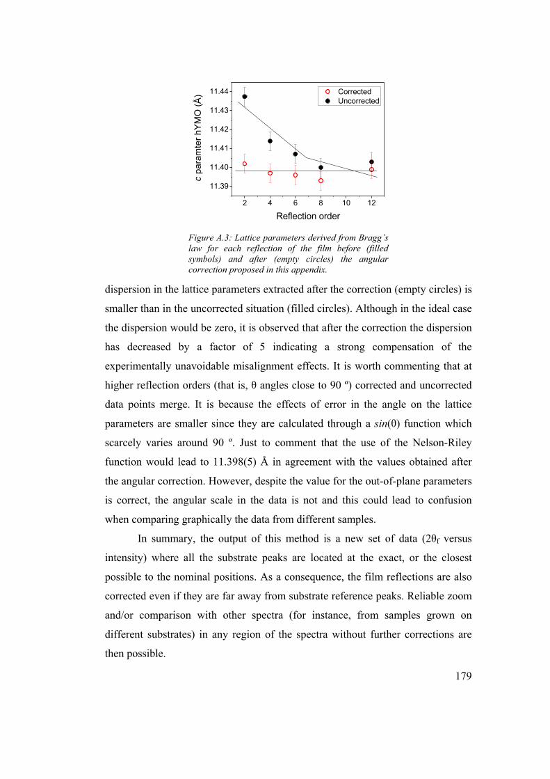
179
2 4 6 8 10 12
11.39
11.40
11.41
11.42
11.43
11.44 Corrected Uncorrected
c pa
ram
ter h
YM
O (Å
)
Reflection order Figure A.3: Lattice parameters derived from Bragg’s law for each reflection of the film before (filled symbols) and after (empty circles) the angular correction proposed in this appendix.
dispersion in the lattice parameters extracted after the correction (empty circles) is
smaller than in the uncorrected situation (filled circles). Although in the ideal case
the dispersion would be zero, it is observed that after the correction the dispersion
has decreased by a factor of 5 indicating a strong compensation of the
experimentally unavoidable misalignment effects. It is worth commenting that at
higher reflection orders (that is, θ angles close to 90 º) corrected and uncorrected
data points merge. It is because the effects of error in the angle on the lattice
parameters are smaller since they are calculated through a sin(θ) function which
scarcely varies around 90 º. Just to comment that the use of the Nelson-Riley
function would lead to 11.398(5) Å in agreement with the values obtained after
the angular correction. However, despite the value for the out-of-plane parameters
is correct, the angular scale in the data is not and this could lead to confusion
when comparing graphically the data from different samples.
In summary, the output of this method is a new set of data (2θf versus
intensity) where all the substrate peaks are located at the exact, or the closest
possible to the nominal positions. As a consequence, the film reflections are also
corrected even if they are far away from substrate reference peaks. Reliable zoom
and/or comparison with other spectra (for instance, from samples grown on
different substrates) in any region of the spectra without further corrections are
then possible.


181
Figure B.1: (a) Raw data from a XRR experiment. (b) Reflectivity and its derivative displaying the marked decay at the critical angle. (c) Reflectivity presented in reciprocal space units. (d) FFT of the data in panel (c).
Appendix B: X-ray reflectivity with FFT
Determining the thickness is perhaps one of the most critical steps towards
quantification in magnetic measurements. For instance, the slope in a 1/χ curve
has units of (Oe·g/emu). Since the mass is proportional to the thickness, an
incorrect increase of 5% in the thickness implies an increase of 5% in the effective
magnetic moment. Since the magnetic signal is proportional to thickness, thicker
films are easier to measure by SQUID but, on the other hand, the determination of
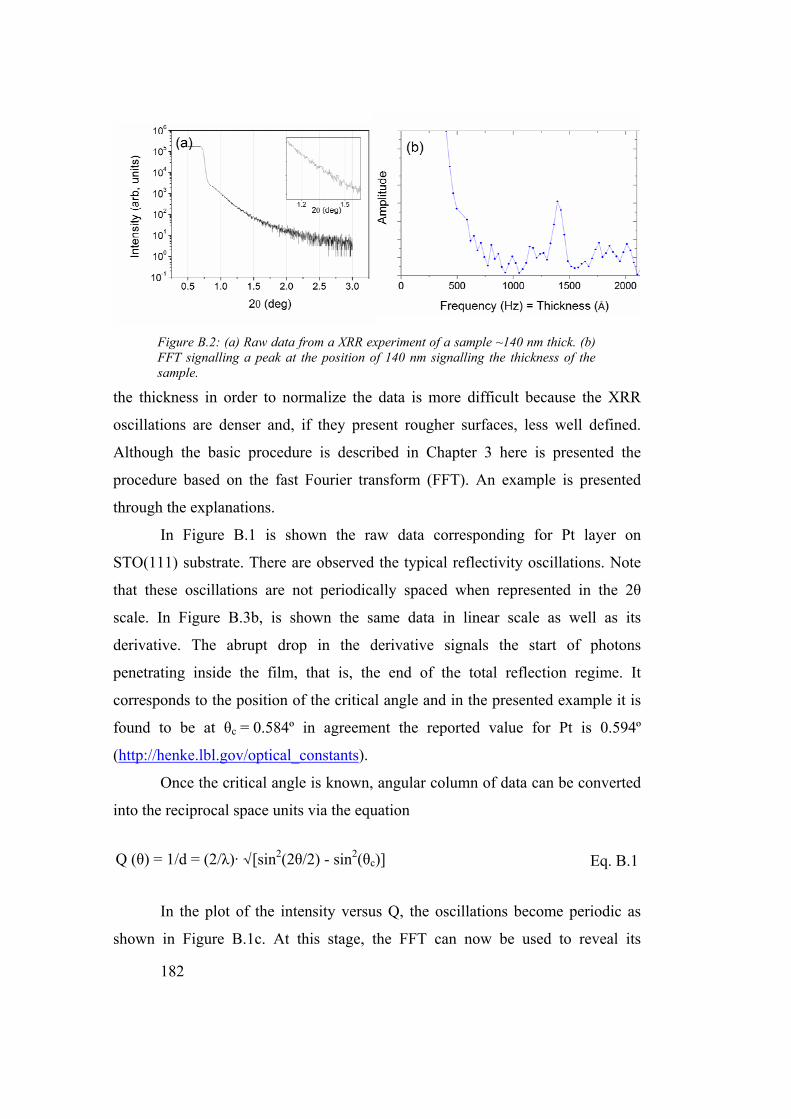
182
Figure B.2: (a) Raw data from a XRR experiment of a sample ~140 nm thick. (b) FFT signalling a peak at the position of 140 nm signalling the thickness of the sample.
the thickness in order to normalize the data is more difficult because the XRR
oscillations are denser and, if they present rougher surfaces, less well defined.
Although the basic procedure is described in Chapter 3 here is presented the
procedure based on the fast Fourier transform (FFT). An example is presented
through the explanations.
In Figure B.1 is shown the raw data corresponding for Pt layer on
STO(111) substrate. There are observed the typical reflectivity oscillations. Note
that these oscillations are not periodically spaced when represented in the 2θ
scale. In Figure B.3b, is shown the same data in linear scale as well as its
derivative. The abrupt drop in the derivative signals the start of photons
penetrating inside the film, that is, the end of the total reflection regime. It
corresponds to the position of the critical angle and in the presented example it is
found to be at θc = 0.584º in agreement the reported value for Pt is 0.594º
(http://henke.lbl.gov/optical_constants).
Once the critical angle is known, angular column of data can be converted
into the reciprocal space units via the equation
Q (θ) = 1/d = (2/λ)· √[sin2(2θ/2) - sin2(θc)] Eq. B.1
In the plot of the intensity versus Q, the oscillations become periodic as
shown in Figure B.1c. At this stage, the FFT can now be used to reveal its
183
periodicity as shown in Figure B.1d. The peak signals directly the thickness of the
film in the same units as the λ used in Eq. B.1. Note that if the critical angle is not
determined correctly, the oscillations in the reflectivity will not be periodic in the
reciprocal space units and, as a consequence, the FFT will provide a very broad
peak or no peak at all.
The FFT procedure has proved particularly useful in relatively thick films
(t > 125 nm) where the increasing roughness and the decrease of period of the
XRR oscillations are combined to make it difficult even more the standard peak-
picking method described in Chapter 3. An example is given in Figure B.2.
Almost imperceptible oscillations are detected by FFT, clearly out of the noise.


185
Appendix C: detection of ferromagnetic impurities
In Chapter 4 has been investigated the weak-ferromagnetism that arises
from the canting of an antiferromagnetic structure. The measurement of the
antiferromagnetic response in thin films requires all possible precautions to
discriminate the intrinsic signal (which is around 10-5 – 10-6 emus) from the
extrinsic contributions such as the diamagnetic substrate and virtually unavoidable
small paramagnetic or ferromagnetic impurities in laboratory environments.
Here are described the procedures followed for the magnetometry data in
YMnO3 thin films grown on SrTiO3 substrates. First it is shown how to evaluate
the substrate contribution from experimental measurements. Then, it is shown the
procedure to detect ferromagnetic impurities in the measurements and, finally, the
determination of the effective magnetic moment and the extrapolated Curie
temperatures. An example starting from the raw data is presented.
Measurements of SrTiO3 substrates diamagnetism
Data of field dependence measurements at 300 K and 35 K on bare SrTiO3
substrates are shown in Figure C.1. The measurements were performed to the as-
received substrate (5x5 mm2 area, 0.5 mm thick) and the straw, with no additional
teflon or plastic to hold the substrate. The magnetic field was applied in the plane
of the sample.
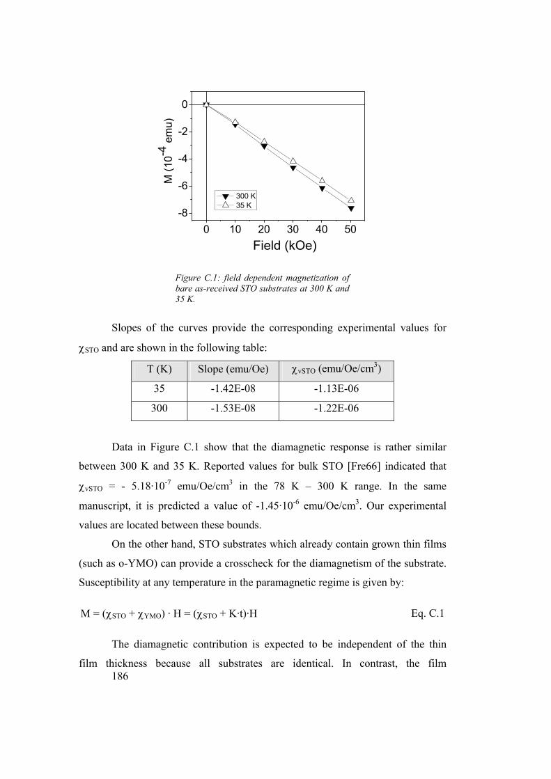
186
0 10 20 30 40 50-8
-6
-4
-2
0
M (1
0-4 e
mu)
Field (kOe)
300 K 35 K
Figure C.1: field dependent magnetization of bare as-received STO substrates at 300 K and 35 K.
Slopes of the curves provide the corresponding experimental values for
χSTO and are shown in the following table:
T (K) Slope (emu/Oe) χvSTO (emu/Oe/cm3)
35 -1.42E-08 -1.13E-06
300 -1.53E-08 -1.22E-06
Data in Figure C.1 show that the diamagnetic response is rather similar
between 300 K and 35 K. Reported values for bulk STO [Fre66] indicated that
χvSTO = - 5.18·10-7 emu/Oe/cm3 in the 78 K – 300 K range. In the same
manuscript, it is predicted a value of -1.45·10-6 emu/Oe/cm3. Our experimental
values are located between these bounds.
On the other hand, STO substrates which already contain grown thin films
(such as o-YMO) can provide a crosscheck for the diamagnetism of the substrate.
Susceptibility at any temperature in the paramagnetic regime is given by:
M = (χSTO + χYMO) · H = (χSTO + K·t)·H Eq. C.1
The diamagnetic contribution is expected to be independent of the thin
film thickness because all substrates are identical. In contrast, the film

187
0 25 50 75 100 125
-8.0x10⁻⁷
-9.0x10⁻⁷
-1.0x10⁻⁶
-1.1x10⁻⁶
-1.2x10⁻⁶
χ S
TO (e
mu/
cm3 /O
e)
Thickness (nm) Figure C.2: susceptibility at 300 K for a set of films grown on STO(001) substrates versus its thickness.
susceptibility depends linearly on the thickness. Then, the field dependent
magnetization curves will display a slope of:
dM/dH = χSTO + K·t Eq. C.2
Hence at the limit of zero thickness (t → 0) the slope in M(H) curves
should correspond to the diamagnetic substrate susceptibility. Data presented in
Figure C.2 supports this expectation. The extrapolated value to zero thickness is in
agreement with the directly measured on bare STO substrates.
χvSTO = (-1.11 ± 0.05) ·10-6 emu/Oe/cm3 Eq. C.3
Determination of ferromagnetic impurities
In the absence of impurities, the total magnetization of our system would
be linear with the applied magnetic field as shown in Eq. C.1. The presence of
ferromagnetic impurities modifies the total magnetization introducing an
additional term:
M = ( χSTO + χYMO(T) ) · H + FM Eq. C.4
If the applied magnetic field is above the coercitive field and the

188
temperature is well below the Curie temperature of the FM, the FM term can be
assumed to be saturated and, thus, independent of the temperature and the
magnetic field. Special attention must be paid to Fe – Ni ferromagnetic impurities
that, due to its large saturation magnetization, in very tiny amounts can introduce
large additional magnetic signal in the measurements. By measuring with
magnetic fields larger than 10 kOe and temperatures below 300 K the conditions
for magnetic saturation of such impurities are fulfilled.
A linear relationship between M and H can be written if several
magnetization curves Mi(T) are recorded at different magnetic fields (Hi).
Mi = ( χSTO + χYMO(T) ) · Hi + FM = A(T) · Hi + B(T) Eq. C.5
Two curves A(T) and B(T) can be extracted. A(T) accounts for the
paramagnetic response plus the diamagnetic shift of the film and B(T) indicates
the contribution attributed to saturated ferromagnetic impurities. While the A(T)
curve must resemble a Curie-Weiss-like behaviour (plus the diamagnetism by the
STO substrate), the B(T) parameter is expected to present a constant behaviour as
long as the FM contribution is saturated.
After removing the ferromagnetic impurities by subtracting B(T), the
χYMO(T) is obtained as:
χYMO(T) = A(T) - χSTO Eq. C.6
The next action is the elimination of the substrate diamagnetism. In the
case of commercial substrates with stated dimensions the χSTO can be obtained by
multiplying the substrate volume to the value in Eq. C.3. In the case of different
sizes it is possible to weight the substrates (neglecting the weight of the thin film)
using a microbalance and compute the volume through the nominal STO density,
5.12 g/cm3. Nominal value for a 5x5 mm2, 500 μm thick, is 64.0 mg.
We now expand the mass susceptibility for the paramagnetic Mn ions in
YMO according to the Curie-Weiss law:

189
χm (T) = C · 1/ (T – θp) Eq. C.7
C is the Curie-Weiss constant for YMO which is C = 1.57·10-2
K·emu/g/Oe in the case of Mn3+ and orthorhombic YMnO3. The effective
magnetic moment has been taken as μeff = 4.90μB. Note that for other materials or
even in the hexagonal YMnO3 this constant would be different.
To obtain a linear behaviour with temperature invert Eq. C.7 is inverted
1/χm (T) = 1/C · (T – θp) Eq. C.8
Note that, at this stage, if the filtering of the substrate and impurities
contributions is performed correctly, susceptibility curves performed at different
large magnetic fields must merge perfectly. Also, 1/χm should present a linear
behaviour at temperatures larger than the transition temperature (neglecting short
range magnetic interactions which are expected to be relevant only in a narrow
temperature range close to the critical temperature). In that case, a linear fit in the
experimental 1/χm (T) curve would be sufficient to obtain C(μeff) and θp.
However, linearity in 1/χm (T) is extremely sensitive to the three adjustable
parameters in our model: substrate diamagnetism, film thickness and substrate
mass. The values are often needed to be optimized within the error bars to obtain a
larger linear correlation. If it is not possible, or the required changes overcome the
error bars in the experimental inputs, our initial model in Eq. C.4 is not suitable
and the results will not be reliable.
Since the fitting in Eq. C.8 involves two free parameters (C and θp), it may
be more interesting to first determine C and next use the obtained value for the
calculation of θp. To this end, the derivative in Eq. C.8 is performed.
d/dT [1/χm (T)] = 1/C Eq. C.9
The calculation of C via Eq. C.9 allows focussing first in μeff and, in a
subsequent step, θp using Eq. C.8. The plot of Eq. C.9 should display a constant
value above the magnetic transition temperature. Subsequently, θp can be obtained
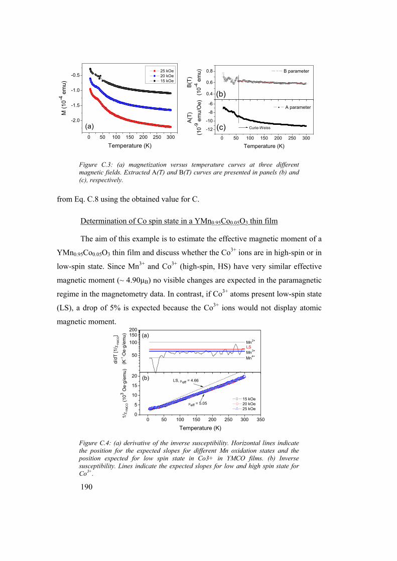
190
0 50 100 150 200 250 300
-2.0
-1.5
-1.0
-0.5
M (1
0-4 e
mu)
Temperature (K)
25 kOe 20 kOe 15 kOe
(a)0 50 100 150 200 250 300
-12
-10
-8
-6
A(T
)
(10-9
em
u/O
e)
Temperature (K)
A parameter
Curie-Weiss
0.4
0.6
0.8
(c)
B(T
)
(10-4
em
u) B parameter
(b)
Figure C.3: (a) magnetization versus temperature curves at three different magnetic fields. Extracted A(T) and B(T) curves are presented in panels (b) and (c), respectively.
0 50 100 150 200 250 300 3500
5
10
15
20
15 kOe 20 kOe 25 kOe
(b)
1/χ Y
MC
O (1
03 Oe·
g/em
u)
Temperature (K)
LS, μeff = 4.66
μeff = 5.05
50
100150200
Mn3+
Mn4+
LS
d/dT
[1/χ
YM
CO]
(K-1·O
e·g/
emu) (a)
Mn2+
Figure C.4: (a) derivative of the inverse susceptibility. Horizontal lines indicate the position for the expected slopes for different Mn oxidation states and the position expected for low spin state in Co3+ in YMCO films. (b) Inverse susceptibility. Lines indicate the expected slopes for low and high spin state for Co3+.
from Eq. C.8 using the obtained value for C.
Determination of Co spin state in a YMn0.95Co0.05O3 thin film
The aim of this example is to estimate the effective magnetic moment of a
YMn0.95Co0.05O3 thin film and discuss whether the Co3+ ions are in high-spin or in
low-spin state. Since Mn3+ and Co3+ (high-spin, HS) have very similar effective
magnetic moment (~ 4.90μB) no visible changes are expected in the paramagnetic
regime in the magnetometry data. In contrast, if Co3+ atoms present low-spin state
(LS), a drop of 5% is expected because the Co3+ ions would not display atomic
magnetic moment.

191
Prior to the magnetic measurements, characterizations of the samples
revealed that film thickness was 137(5) nm and weight of the substrate was
55.3(5) mg. Figure C.3a shows the raw data obtained in M(T) curves performed at
15, 20 and 25 kOe from 300 K to 5 K at cooling rate of 2 K/min. The magnetic
field is applied in the plane of the samples. Solid lines correspond to the
interpolation and smoothing of the raw data. Panels b and c show the extracted
A(T) and B(T) curves, respectively. As expected, a spurious ferromagnetic
contribution is found to be essentially constant and only a very tiny slope is
observed in the whole paramagnetic range down to the magnetic transition
temperature. In contrast, the shape of the A(T) contribution resembles the typical
~ 1/T paramagnetic behaviour.
From the weight m of the sample, the volume is obtained as Vf = ρ·m. and
the substrate contribution is χvSTO·Vf. Accordingly, 1.20·10-8 emu/Oe were added
in the A(T) curve to compensate the substrate diamagnetism. The inverse
susceptibility of A(T) is shown in Figure C.4a. The theoretical positions of Mn2+,
Mn3+ and Mn4+ are represented as horizontal lines. Results indicate that the
measured effective magnetic moment is closer to Mn3+ and, thus, to HS than to a
LS line. It is more evident from the 1/χ plot shown in panel b that the slope
matches better the HS state than the LS state. Moreover, the three 1/χ curves
performed at three different magnetic fields merge and are linear with the
temperature in the paramagnetic regime as expected after the procedures. Finally,
from the extrapolation of the paramagnetic slope, it is found that θp = - 20 K
indicating dominating Mn-O-Mn antiferromagnetic interactions.


193
20 40 60 80 100
(c)
Inte
nsity
(arb
. uni
ts)
2θ (º)
YMO(101)
YMO(303)
YMO(400)YMO(200)
STO(220)STO(110)
YMO(006)YMO(00
4)
YMO(002)
STO(003)
STO(002)STO(001)
YMO
(404
)
YMO(202)
STO(222)
STO(111) (b)
(a)
Figure D.1: θ/2θ scans of oYMO films grown on (a) (001), (b) (110) and (c) (111) oriented STO substrates.
Appendix D: domain structure and texture selection in orthorhombic YMnO3 thin films
In Chapter 4 is described how ferromagnetism is induced by epitaxial
strain in oYMO thin films grown on STO(001) substrates. The use of substrates
with different out-of-plane orientation would provide new mismatch scenarios
were the film’s texture, the epitaxial strain and the amount of crystal domains are
different. On the other hand, in Chapter 5 has been observed that YMO films
grown directly on STO(111) substrates are orthorhombic and not hexagonal as it
could be expected from the three-fold symmetry of the substrate. In this appendix

194
0 90 180 270 360
o-YMO(001)/STO(001)
Inte
nsity
(arb
. uni
ts)
φ (deg)0 90 180 270 360
o-YMO(100)/STO(110)
φ (deg)
0 90 180 270 360
o-YMO(101)/STO(111)
Inte
nsity
(arb
. uni
ts)
φ (deg)0 90 180 270 360
h-YMO(0001)/Pt(111)/STO(111)
φ (deg)
h-YMO(111)
Pt(220)
o-YMO(112)
STO(220)
STO(111)
(c) (d)
(b)(a) o-YMO(111)
STO(110)
o-YMO(200)
Figure D.2: φ-scans of the YMO films on STO substrates (001), (110) and (111) (a, b, and c, respectively) and Pt/STO(111) substrate (d). The measured reflections are indicated.
both issues are discussed sequentially.
Crystal texture and domain structure selection in YMO/STO films
YMO films were grown by pulsed laser deposition on (001), (110) and
(111) oriented substrates. In Figure D.1 is shown the XRD θ/2θ scan for the 50
nm thick films grown at 800 ºC, 0.2 mbar. In all cases, only reflections associated
to the orthorhombic phase can be identified. The films are textured, with the out-
of-plane orientation different in each substrate. Using the Pbnm setting for YMO
the scans indicate that the films have grown textured as YMO(001)/STO(001),
YMO(101)/STO(111) and YMO(100)/STO(110).
On the other hand, the in-plane texture of these films has been investigated
by using φ-scans and pole figures. Figure D.2 (panels a, b, c, d) collects the φ-
scans corresponding to reflections of the films grown directly on STO substrates
and compared to one Pt(111) buffered film on STO(111) substrate.
Data in Figure 2 indicate that the films grown are epitaxial. In panel a,

195
corresponding to the YMO(001)/STO(001) film, one can appreciate the
occurrence of two sets of reflections indicating that two domains, in plane rotated
90º, coexist in the films. The epitaxial relationships
[100]YMO(001)/[110]STO(001) and [010]YMO(001)/[110]STO(001) are
obtained as mentioned in Chapter 4.
The φ-scans of the YMO(112) reflections of the YMO(100)/STO(110) are
shown in panel b. Two sets of a pair of peaks, separated by Δφ = 113.7º, which
arise from the orthorhombic symmetry of YMO, are observed and it indicates that
the film has grown epitaxially and presents a single domain structure. The
epitaxial relationship is found to be [001]YMO(100) / [001]STO(110).
Finally, in panel c, the φ-scans of the YMO(200) reflection (bottom panel)
and the STO(110) reflections (top panel) of the YMO(101)/STO(111) are shown.
The φ-scan of the (200) reflection of an epitaxial YMO film out-of-plane (101)-
oriented should present only one peak according to an orthorhombic symmetry.
However, there are three peaks 120º apart, signalling the presence of three crystal
domains characterized by an in-plane rotation of 120º. This structure of domains
is a direct consequence of the STO(111) surface symmetry under 120º rotations.
The epitaxial relationships of the domains are [101]YMO(101) / [112]STO(111),
[101]YMO(101) / [121]STO(111) and [101]YMO(101) / [211]STO(111). For the
aim of comparison it is also presented the ϕ-scan for a film grown on 7.2 nm thick
Pt buffer layer on STO(111). Data indicate that the YMO film is hexagonal.
In Figure D.3 are illustrated the epitaxial relationships obtained from the
ϕ-scans for the films grown on the three orientations for the STO substrates.
Next, the epitaxial stabilization of the orthorhombic phase and the
formation of crystal domains are discussed. As it was mentioned in the
introduction chapter, YMO can present either hexagonal or orthorhombic phase.
However, only the hexagonal phase is found in bulk samples; the orthorhombic
phase has been only obtained by high-pressure synthesis or by soft-chemistry
methods. In a more general context, the stabilization in thin films of phases that
are abnormal in bulk was theoretically studied by Jesser [Jes69], and he concluded

196
Figure D.3: Schematic drawings to illustrate the epitaxial relationships and the domain structures deduced from the analysis of the measured φ-scans: (a) YMO(001) on STO(001); (b) YMO(101) on STO(111); and (c) YMO(100) on STO(110).
that in certain cases it is energetically favourable for a film to stabilize in the same
crystal structure as that the substrate rather than in the structure stable in bulk. In
particular, this has been observed in some oxide thin films, including manganites
as YMO, in which an unfavorable phase can be stabilized if it can grow
pseudomorphically with the substrate [Gor02, Gra03]. On the other hand, it has
also been suggested that the sign of the epitaxial stress (compressive or tensile) is
the main factor in the selection of the orthorhombic or hexagonal phase in YMO
films [Dho04]. We note that the selection of the phase is determined at the early
growth stages when stable islands form. In the case of STO(001) and STO(110)
surfaces, there is high compatibility of symmetry with orthorhombic YMO (o-
YMO), whereas hexagonal YMO (hex-YMO) should be incommensurate and thus
its epitaxial growth is not likely to occur. On the contrary, the 120º-rotation

197
(a) (b) (c)Manganese oxide layerYttrium oxide layerStrontium titanate
o-YMO(001)[010]o-YMO →
o-YMO(001)[010]o-YMO →
STO(111)[101]STO →
Figure D.4: Sketches of the atomic arrangements at the (a) STO(001) surface (strontium oxide termination), and at the o-YMO(001) surface with (b) yttrium oxide and (b) manganese oxide terminations. Blue spheres correspond to oxygen atoms. Other spheres correspond to (a) strontium, (b) yttrium, and (c) manganese atoms.
symmetry of the STO(111) surface appears to be compatible with both the o-
YMO phase and the hex-YMO phase. Indeed, although the films on STO(111)
reported here are formed by a single o-YMO phase, Dho et al. [Dho04] found
coexistence of both o-YMO and hex-YMO phases. On the other hand, it is
remarkable that although being the Pt and STO lattice parameters almost identical
at room temperature, epitaxial hex-YMO is always obtained on Pt(111) thicker
than 7 nm buffered STO(111). Therefore, it follows that the sign of the epitaxial
stress does not appear to be the major factor in YMO phase selection. In the case
of the competing phase selection of compounds with cubic structure on (111)
surfaces, other aspects, as electronic interactions, could determine the YMO
phase. Moreover, it has to be noted that the matching of the oxygen sub-lattices at
the interface can be determinant in heteroepitaxy of oxides, but this relevance is
obviously absent in the case of growth on platinum.
To illustrate the discussion in the previous paragraph are shown in Figure
D.4 the STO(111) surface (panel a) and the o-YMO(001) surfaces at both the
yttrium oxide (panel b) and manganese oxide (panel c). The similarities of the
oxygen sub-lattices are not observed when comparing STO(111) surface with o-
YMO(001) manganese oxide termination (panel c) but, in contrast, they become
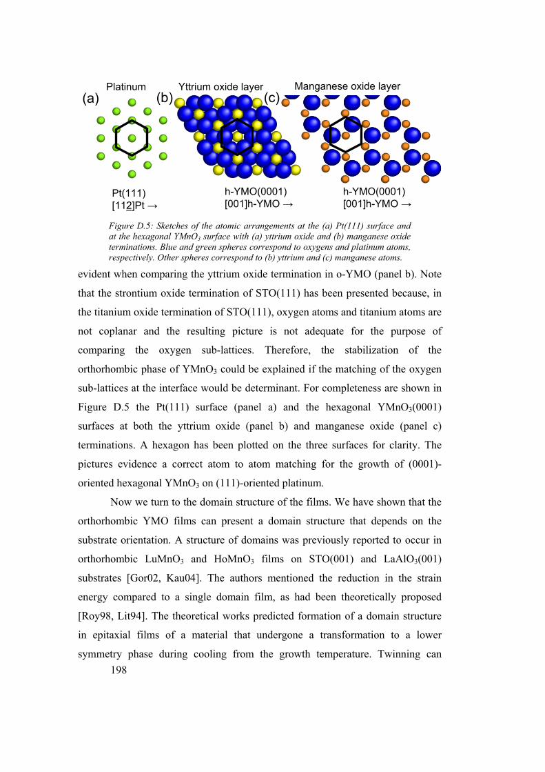
198
Pt(111)[112]Pt →
h-YMO(0001)[001]h-YMO →
h-YMO(0001)[001]h-YMO →
(a) (b) (c)Manganese oxide layerYttrium oxide layerPlatinum
Figure D.5: Sketches of the atomic arrangements at the (a) Pt(111) surface and at the hexagonal YMnO3 surface with (a) yttrium oxide and (b) manganese oxide terminations. Blue and green spheres correspond to oxygens and platinum atoms, respectively. Other spheres correspond to (b) yttrium and (c) manganese atoms.
evident when comparing the yttrium oxide termination in o-YMO (panel b). Note
that the strontium oxide termination of STO(111) has been presented because, in
the titanium oxide termination of STO(111), oxygen atoms and titanium atoms are
not coplanar and the resulting picture is not adequate for the purpose of
comparing the oxygen sub-lattices. Therefore, the stabilization of the
orthorhombic phase of YMnO3 could be explained if the matching of the oxygen
sub-lattices at the interface would be determinant. For completeness are shown in
Figure D.5 the Pt(111) surface (panel a) and the hexagonal YMnO3(0001)
surfaces at both the yttrium oxide (panel b) and manganese oxide (panel c)
terminations. A hexagon has been plotted on the three surfaces for clarity. The
pictures evidence a correct atom to atom matching for the growth of (0001)-
oriented hexagonal YMnO3 on (111)-oriented platinum.
Now we turn to the domain structure of the films. We have shown that the
orthorhombic YMO films can present a domain structure that depends on the
substrate orientation. A structure of domains was previously reported to occur in
orthorhombic LuMnO3 and HoMnO3 films on STO(001) and LaAlO3(001)
substrates [Gor02, Kau04]. The authors mentioned the reduction in the strain
energy compared to a single domain film, as had been theoretically proposed
[Roy98, Lit94]. The theoretical works predicted formation of a domain structure
in epitaxial films of a material that undergone a transformation to a lower
symmetry phase during cooling from the growth temperature. Twinning can
199
reduce the energy if the two variants had lattice parameters above and below the
substrate lattice parameter as the present case in o-YMO(001)/STO(001) films.
The ferroelectric PbTiO3 is a paradigmatic material in which the formation of a
domain structure has been observed and analyzed [Pom93, Alp98]. However, this
is not the only source of twinning in epitaxial films.
In the case of the epitaxy of YMO on STO substrates, the lattice mismatch
is of opposite sign for the two in-plane perpendicular directions in each of the
three orientations investigated. Films can grow coherently onto the substrate,
before partial relaxation above a critical thickness or during cooling down. When
the YMO films relax, they undergo a transformation from the cell imposed by the
substrate (due to the coherent growth), to an orthorhombic cell (close to the one of
the bulk YMO). A film partially strained accumulates an excess of energy,
proportional to the square of the strain in the case of systems with biaxial
symmetry [Mat75]. In the case of orthorhombic YMO the lattice mismatch with
STO is of opposite sign along different in-plane directions, and then a domain
structure can reduce the strain energy in the film. The YMO films can thus be
tensile and compressively periodically stressed along a certain direction. In the
twinned film, the lattice strain due to the macroscopic clamping imposed by the
substrate should be more easily accommodated, although at the expense of an
additional energy in the domain walls. To consider the population of each domain
we note that strain has to be accommodated along each principal directions of
film, and thus the same percentage of domains is expected, even when the
magnitude of strain differs along each direction. On the other hand, the elastic
energy accumulated in a film with strained polydomains increases also linearly
with thickness, and thus the films relax above a critical thickness.
Finally, we note that although in a general case a polydomain structure can
be energetically favourable in orthorhombic films, some particular domains can
be unfavourable. In particular, in epitaxial films, those domains that can not grow
epitaxially on the substrate will not form. We have observed that YMO(001) films
on STO(001) substrates present two variants, YMO(101) on STO(111) three, and
YMO(100) on STO(110) are single domain. Thus, the number of variants appears

200
30 31 32 33 34 35700 / t
2θ (deg)
750 / tIn
tens
ity (a
rb. u
nits
)
800 / t
850 / t
STO(110) oYMO(200)
900 / t
oYMO(020)
Figure D.6: Zoom of θ/2θ scans around the STO(110) reflection for o-YMO films as a function of the substrate temperature. Vertical lines signal the position for bulk reflections as labelled.
to be restricted by the symmetry of the two-dimensional crystal lattice of the
surface of the used substrate.
Control of the out-of-plane texture in single domain films
In Chapter 4 it has been shown that films grown on STO(001) present two
in-plane crystal domains and the corresponding magnetic properties have been
discussed. Therefore, the next step would be to obtain single domain films as they
would allow studying the magnetic and magnetodielectric properties along
different crystal directions.
To this end, a series of films were grown by PLD on STO(110) substrates.
In this new series of depositions, the effect of temperature and thickness was
investigated. While PO2 pressure was kept fixed at 0.1 mbar, substrate temperature
was varied in the 700 – 850 ºC range and thickness from t = 120 nm to t/4.
θ/2θ scans around the STO(110) reflection are presented in Figure D.6.
Data show a dependence of the out-of-plane texture with the temperature. b-
oriented films are found at lower temperatures and gradually changing into a-
textured films as temperature increases. For subsequent measurements of the
magnetic anisotropy it is more convenient to have the b-axis in-plane of the
sample. In that situation, measurements along parallel and perpendicular
directions respect to the antiferromagnetic axis ([010]) can be investigated only by
in-plane measurements thus not being necessary to perform demagnetization field

201
(a) (b)
30 31 32 33 34 35850 / t
2θ (deg)
850 / (t/2)In
tens
ity (a
rb. u
nits
)850 / (t/4)
STO(110) oYMO(200)oYMO(020)
30 31 32 33 34 35900 / t
2θ (deg)
900 / (t/2)
Inte
nsity
(arb
. uni
ts)
900 / (t/4)
STO(110) oYMO(200)oYMO(020)
(c)
700 750 800 850 9000
50
100
150
(100) oriented
Thic
knes
s (n
m)
Temperature (ºC)
(100)+(010) oriented
Figure D.7: θ/2θ scans of oYMO/STO(110) films as a function of the thickness of the sample at (a) 850 ºC and (b) 900 ºC. Vertical lines signal the position for bulk reflections as labelled. (c) Diagram showing the conditions (thickness and temperature) where each film orientation is found on o-YMO/STO(110) films..
corrections which are only relevant in out-of-plane measurements. Therefore, the
attention focuses on the a-oriented films with the intention of producing thin films
with a gradual distortion of the unit cell.
To this end, two series of samples were grown at 850 ºC and 900 ºC. Film
thickness was changed aiming to obtain different distortion of the unit cell. θ/2θ
scans are presented in Figure D.7. It is found (panel a) that increasing the
thickness b oriented material is detected even at 850 ºC temperatures. In contrast,
this is not observed at 900 ºC where all the films were a-oriented. The positions of
the peaks in the scans indicate that in b parameter is contracted. Other authors
have also reported this dependency of the out-of-plane texture with the
temperature in ~ 200 nm thick o-YMO films grown on STO(110) substrates
[Hsi08]. Of relevance here, is that angular location of the (200) peaks depend on
the film thickness. This observation is specially evident for films grown at 900 ºC
shown in panel b where the peaks is displaced towards higher angles (indicating a
more contracted b axis) as thickness is reduced.
Therefore, growth of o-YMO on STO(110) allows the selection of the out-
of-plane texture (see Figure D.8) and the epitaxial strain. Next steps would
include a systematic study of the unit cell distortion versus the magnetization and
the growth of the films on Nb-doped substrates for dielectric characterization.