Embed Size (px)
Citation preview

18
Graphene Nanoribbons: from chemistry to
circuits
F. Tseng, D. Unluer, M. R. Stan, and A. W. Ghosh
Charles L Brown School of Electrical and Computer Engineering, University ofVirginia, Charlottesville, VA22901 [email protected]
Summary. The Y-chart is a powerful tool for understanding the relationship be-tween various views (behavioral, structural, physical) of a system, at different lev-els of abstraction, from high-level, architecture and circuits, to low-level, devicesand materials. We thus use the Y-chart adapted for graphene to guide the chap-ter and explore the relationship among the various views and levels of abstraction.We start with the innermost level, namely, the structural and chemical view. Theedge chemistry of patterned graphene nanoribbons (GNR) lies intermediate betweengraphene and benzene, and the corresponding strain lifts the degeneracy that other-wise promotes metallicity in bulk graphene. At the same time, roughness at the edgeswashes out chiral signatures, making the nanoribbon width the principal arbiter ofmetallicity. The width-dependent conductivity allows the design of a monolithicallypatterned wide-narrow-wide all graphene interconnect-channel heterostructure. Ina three-terminal incarnation, this geometry exhibits superior electrostatics, a cor-respondingly benign short-channel effect and a reduction in the contact Schottkybarrier through covalent bonding. However, the small bandgaps make the devicestransparent to band-to-band tunneling. Increasing the gap with width confinement(or other ways to break the sublattice symmetry) is projected to reduce the mobil-ity even for very pure samples, through a fundamental asymptotic constraint on thebandstructure. An analogous trade-off, ultimately between error rate (reliability)and delay (switching speed) can be projected to persist for all graphitic derivatives.Proceeding thus to a higher level, a compact model is presented to capture the com-plex nanoribbon circuits, culminating in inverter characteristics, design metrics andlayout diagrams.
The Gajski-Kuhn Y-chart (Fig. 18.1) is a model which captures in a snap-shot view, the essential considerations in designing semiconductor devices [1].The three domains of the Gajski-Kuhn Y-chart are on radial axes. Each ofthe domains can be divided into levels of abstraction, using concentric rings.At the top level (outer ring), we consider the architecture of the chip; at thelower levels (inner rings), we successively refine the design into finer detailedimplementation:
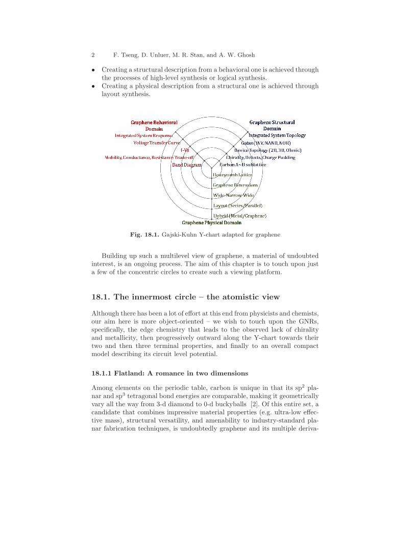
2 F. Tseng, D. Unluer, M. R. Stan, and A. W. Ghosh
• Creating a structural description from a behavioral one is achieved throughthe processes of high-level synthesis or logical synthesis.
• Creating a physical description from a structural one is achieved throughlayout synthesis.
Fig. 18.1. Gajski-Kuhn Y-chart adapted for graphene
Building up such a multilevel view of graphene, a material of undoubtedinterest, is an ongoing process. The aim of this chapter is to touch upon justa few of the concentric circles to create such a viewing platform.
18.1. The innermost circle – the atomistic view
Although there has been a lot of effort at this end from physicists and chemists,our aim here is more object-oriented – we wish to touch upon the GNRs,specifically, the edge chemistry that leads to the observed lack of chiralityand metallicity, then progressively outward along the Y-chart towards theirtwo and then three terminal properties, and finally to an overall compactmodel describing its circuit level potential.
18.1.1 Flatland: A romance in two dimensions
Among elements on the periodic table, carbon is unique in that its sp2 pla-nar and sp3 tetragonal bond energies are comparable, making it geometricallyvary all the way from 3-d diamond to 0-d buckyballs [2]. Of this entire set, acandidate that combines impressive material properties (e.g. ultra-low effec-tive mass), structural versatility, and amenability to industry-standard pla-nar fabrication techniques, is undoubtedly graphene and its multiple deriva-

18 Graphene Nanoribbons: from chemistry to circuits 3
tives, including carbon nanotubes (CNTs), bilayer graphene (BLG), epitaxialgraphene (epi-G), strained graphene (sG) and graphene nanoribbons (GNR).
The impressive electronic properties of CNTs and GNRs stem from theirparent graphitic bandstructure [3]. Without delving into the mathematics,it is important to rehash some of the salient features relating the bandstruc-ture to the underlying chemistry. The hybridization of one s and two car-bon px,y-orbitals creates a planar honeycomb structure in a single graphenesheet, loosely resembling self-assembled benzene molecules minus the hydro-gen atoms. The crystal structure can be described as a triangular networkwith a two-atom dimer basis, whose π electrons hybridize to create bonding-antibonding pairs that delocalize over the entire crystal to generate conduc-tion and valence bands. However, since the two basis atoms and the orbitalsinvolved are identical, we get a zero-band gap metal with a dispersion re-sembling photons, albeit with a much lower speed. The resulting low energylinear dispersion corresponds to a constant slope and thus a constant velocityv = ∂E/~∂k.
The unique bandstructure of graphene contributes to its amazing elec-tronic properties [2]. Because the Fermi velocity is energy-independent, thecyclotron effective mass of graphene electrons, m∗ = ~kF /vF is vanishinglysmall at low energy (kF → 0, vF being constant at roughly 108 cm/s). Fur-thermore, the two bands are derived out of symmetric and antisymmetric(bonding and antibonding) combinations of the two identical dimer atoms,creating a two component pseudo-spinor out of the two Bloch wavevectors,with their ratio being just a phase factor eiθ, where tan θ = ky/kx relateselectron quasi-momentum components in the graphene x-y plane. The rever-sal of phase between the forward and backward velocity vectors suppresses1D acoustic phonon back-scattering, allowing only Umklapp processes in con-fined graphitic structures such as CNTs and GNRs. The combination of lowmass m∗ and high mean free path λ ultimately leads to very high mobilitiesµ = qλ/m∗vF , with a record room-temperature value at 230,000 cm2/V s [4]for suspended graphene sheets.
In the following sections, we discuss two bandstructure related issues thatarise when we attempt to pattern or modify graphene to generate gapped orconfined planar structures -
• the absence of metallicity and chirality dependent bandgaps in multipleexperiments (sections 18.1.2-18.1.4), and
• the increase in effective mass as a gap is progressively opened, arising fromfundamental asymptotic constraints (section 18.1.5) that are expected topersist even for very pure samples.
18.1.2 Whither metallicity?
The bandstructure of CNTs is by now, a textbook homework problem. Sincethe conduction and valence bands of its parent graphene structure touch pre-cisely at the vertices of its hexagonal Brillouin zone, the Fermi wavelength of

4 F. Tseng, D. Unluer, M. R. Stan, and A. W. Ghosh
undoped graphene corresponds to a unique electron wavelength λF = 3√3R/2,
where R is the C-C bond distance. The imposition of periodic boundary con-ditions along the circumference of a CNT filters out many allowed electronwavelengths and allows only modes that have integer ratios of πD/λ (D beingthe tube diameter), so that a particular chirality (i.e., a wrapping topology)may or may not support λF needed to sustain metallicity. Accordingly, one canderive selection rules on paper, or using simple 1-orbital orthogonal nearestneighbor tight binding, that matches experiments quite well. In any randomarray of CNTs, roughly a third are expected to be metallic, and impressiveprogress has been achieved in sorting them out from their semiconductingcounterparts. Even in extremely narrow CNTs with strong curvature-inducedout-of-plane hybridizations, the anomalous bandgaps are well captured bynon-orthogonal tight-binding formulations such as Extended Huckel Theory[5]. The bandgaps of CNTs bear relatively few surprises, at the end of theday.
Fig. 18.2. (Left) Tight-binding 1-orbital calculations show three chiral curves, oneof which is metallic [6]. In contrast, data from (center) Philip Kim’s group [7] and(right) Hongjie Dai’s group [8] show a single chirality free curve with no metallicsignatures.
Life is more complicated when dealing with GNRs. Indeed, it seems rea-sonable to expect a chirality dependence to arise for GNRs, simply replacingthe periodic circumferential boundary conditions across CNTs with hard-wallboundary conditions across the GNR width. A few details may change, forinstance, we now fit half-wavelengths rather than whole wave-lengths, andthe edges are not completely opaque to electrons tunneling outwards so thatthe boundary conditions are more ‘diffuse’. The quantization condition willroughly correspond now to integer ratios for (W + R
√3)/λ (accounting for
two unit cells outside for the wavefunction to vanish). However, one-orbitaltight binding would still predict three chiral classes in GNRs, one of which isstrictly metallic as in CNTs. Experimentally however, no chirality dependenceis observed for GNRs, nor are any GNRs observed to be strictly metallic atlow temperature (Fig. 18.2). Regardless of wrapping vector, GNRs wider than

18 Graphene Nanoribbons: from chemistry to circuits 5
10 nm are quasi-metallic while narrow ones semiconducting. We thus have astartling disconnect between simple theories and experiments [8].
18.1.3. Edge chemistry – benzene or graphene?
Fig. 18.3. C-C bond length comparisons show that relaxed armchair GNR edges liebetween benzene and double bonds, enjoying only a partial resonant hybridization.
The disconnect between naive expectations and observations arises fromthe boundaries, which ultimately impact the quantization rules behind pat-terned GNRs. Specifically, we argue that edge strain and roughness are themain factors behind the disconnect. Doing justice to such effects will needa proper bandstructure that can capture atomistic chemistry and distortion.While Density Functional Theory (DFT) within the LDA-GGA approxima-tion captures these effects well, we used DFT primarily for structure evalua-tion, and resorted to Extended Huckel theory (EHT) fitted to bulk grapheneto explore the low-energy bandstructures. We relaxed the hydrogenated edgesof armchair GNRs using LDA-GGA and found a bonding environment dis-tinct from bulk graphene. While the inner carbon atoms have a bond-length of1.42A, the edges tend to dimerize and see a 3.5% [6] [9] strain associated witha reduction in bond length to 1.37A. Thereafter, we employ non-orthogonalbasis sets in EHT to capture the effect of the edge chemistry on the low-energyelectronic structure.
There is an appealingly simple explanation for the observed bonding chem-istry. Since the edge atoms are connected to hydrogen on one side and carbonon the other, the difference in electronegativity tends to move the edge C-Catoms closer to a benzene structure (Fig. 18.3). However, the unequal bondingenvironment at the edge disallows any resonant hybridization that evens outthe double-single bond distribution in aromatic rings, so that the edge ringsin GNRs break into ‘domains’ with nearly intact double bonds at the edgesand slightly expanded single bonds towards the bulk end. Since benzene issemiconducting, the 3.5% strain at the dimerized edges increases intradimeroverlap but reduces interdimer overlap, effectively opening a bandgap by 5%.

6 F. Tseng, D. Unluer, M. R. Stan, and A. W. Ghosh
The obvious consequence is that all armchair GNRs become strictly semicon-
ducting, in sharp contrast to their CNT counterparts. In contrast, the edgesof zigzag GNRs have a lateral symmetry that makes them resistant to dimer-ization. In fact, the inward motion of the C-C edges away from the hydrogensshrinks both bond lengths equally, making zigzag edges more conducting.
To calculate the impact of the relaxed bonds on the electronic structure, wecalculated the density of states of a uniformly wide armchair GNR with edgerelaxation using Extended Huckel Theory. While EHT has been used widelyto study molecular properties, it has also been extended to describe bulksemiconducting bandstructures using localized Wannier like non-orthogonalbasis sets that still retain their individual orbital properties. Through exten-sive tests on both graphene and silicon, we have found that EHT accuratelycaptures both bulk bandstructures as well as surface and edge distorted band-structures [10]. The result of our simulation is shown in Fig. 18.4. The roleof edge passivation is shown at the top, where we can see the explicit removalof edge induced midgap states by hydrogenation. The bottom panels showthe role of edge strain. In contrast to pz based nearest neighbor one orbitaltight-binding theory, a small bandgap opens [5]. While CNTs have preciseperiodic boundary conditions along their circumference, the edge atoms donot provide an exact hard wall boundary condition, as the electrons tend totunnel out into the surrounding region. In the presence of edge relaxation,the gap increases because of the aforementioned dimerization, removing anysemblance of metallicity from the bandgap vs width plots.
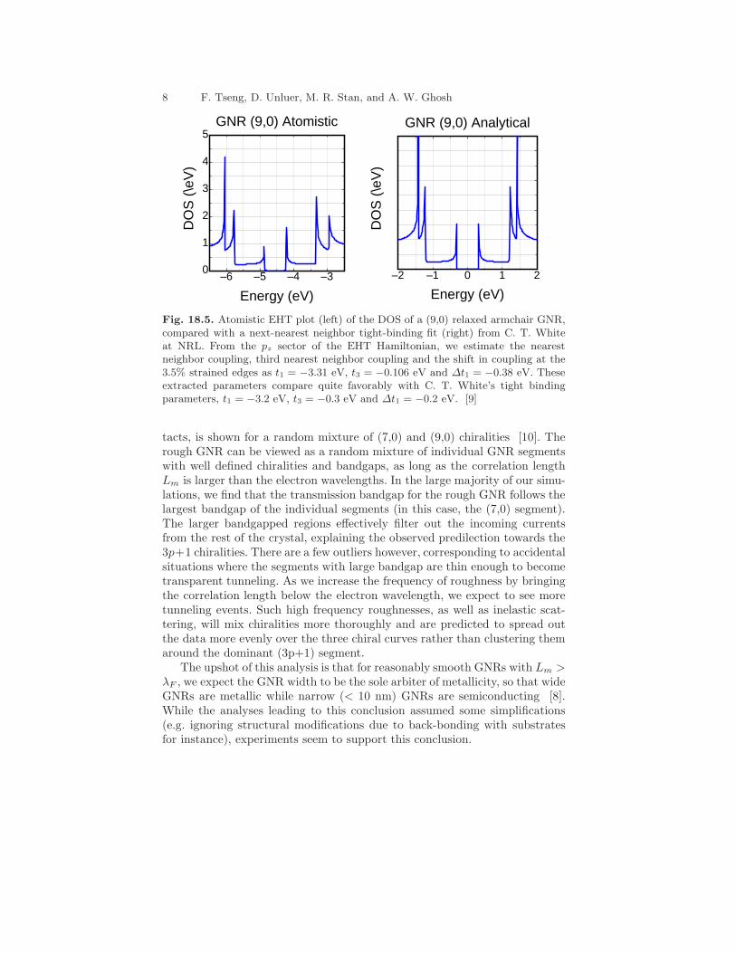
While EHT explains the removal of metallicity, compact models prefer asuitably calibrated orthogonal tight-binding model, with the edge chemistrythrough beyond nearest neighbor interactions. It is not clear if this reproducesthe Bloch wavefunctions, but they do seem to capture the overall density ofstates. Fig. 18.5 shows a comparison between a (9,0) EHT DOS and a (9,0)tight-binding Density of States (DOS) (parametrized independently by CTWhite) [11]. We will use this formulation for our simpler compact modelsdescribed later.
18.1.4. Whither chirality?
While we can explain away the lack of metallicity through the preponderanceof edge strain, why do we not see the three chiral curves in a plot of experi-mentally measured bandgaps versus ribbon widths? The primary reason, webelieve, is roughness at the edges, which tends to wash away such chiral sig-natures. Currently, line edge roughness along a GNR edge is an unavoidableconsequence of lithographic and chemical fabrication techniques [12] [13].Unzipping CNTs via ion bombardment produces the smoothest GNR edgesto date [14]. However edge fluctuations even on the scale of a single atom candegrade transmission probability of modes near band edges, which have im-plications we expound in later sections on material and device characteristicssuch as mobility, subthreshold swing, and ON-OFF ratio.

18 Graphene Nanoribbons: from chemistry to circuits 7
Fig. 18.4. (a) Open carbon bonds at the edges introduce edge-states (shaded) inthe DOS. Spatial resolution of those eigenstates around the Fermi energy confirmsthe electron wavefunction localized at the armchair edges. (b) When open carbonbonds are hydrogen terminated, those edge-states are removed. (c) Applying EHTto GNR dispersion relation across a range of sub-10nm armchair edge widths findsan oscillating bandgap. (d) Relaxation of edge bonds that are hydrogen terminatedwidens the energy bandgap for 3p and reduces the gap for 3p+1 GNRs. Eg vs widthresults are within range of experimental data points [8] and also in agreement withDFT predictions.
We have studied a wide spectrum of line edge roughnesses that can ulti-mately be classified as either a width modulation or width dislocation. Mod-ulation in width along the armchair edge has a corresponding modulationin bandgap that follows an oscillating inverse square law relation betweenbandgap and width, spanning the three chiral curves. Meanwhile a width dis-location is an in-plane displacement in the GNR that energetically sees thesame bandgap at interface of the slip dislocation, albeit with localized interfa-cial states. We introduced edge roughness in our geometries using a Gaussianwhite noise that adds or removes an integer number of dimer pairs with a cor-relation length Lm [11]. The results of our EHT simulations with a statisticsof rough edges explain why measured data are seen to cluster around one the3p+ 1 chirality curves.
An E-k relation cannot be rigorously defined for a structure without peri-odicity, so we focus instead on the transmission bandgap of the entire struc-ture, calculated using the Non-Equilibrium Green’s Function (NEGF) formal-ism in its simplest, Landauer level implementation. The plotted transmissionof the rough segment (Fig. 18.6), sandwiched between two bulk metallic con-
8 F. Tseng, D. Unluer, M. R. Stan, and A. W. Ghosh
–6 –5 –4 –30
1
2
3
4
5
Energy (eV)
DO
S (
\eV
)
GNR (9,0) Atomistic
–2 –1 0 1 2
Energy (eV)
DO
S (
\eV
)
GNR (9,0) Analytical
Fig. 18.5. Atomistic EHT plot (left) of the DOS of a (9,0) relaxed armchair GNR,compared with a next-nearest neighbor tight-binding fit (right) from C. T. Whiteat NRL. From the pz sector of the EHT Hamiltonian, we estimate the nearestneighbor coupling, third nearest neighbor coupling and the shift in coupling at the3.5% strained edges as t1 = −3.31 eV, t3 = −0.106 eV and ∆t1 = −0.38 eV. Theseextracted parameters compare quite favorably with C. T. White’s tight bindingparameters, t1 = −3.2 eV, t3 = −0.3 eV and ∆t1 = −0.2 eV. [9]
tacts, is shown for a random mixture of (7,0) and (9,0) chiralities [10]. Therough GNR can be viewed as a random mixture of individual GNR segmentswith well defined chiralities and bandgaps, as long as the correlation lengthLm is larger than the electron wavelengths. In the large majority of our simu-lations, we find that the transmission bandgap for the rough GNR follows thelargest bandgap of the individual segments (in this case, the (7,0) segment).The larger bandgapped regions effectively filter out the incoming currentsfrom the rest of the crystal, explaining the observed predilection towards the3p+1 chiralities. There are a few outliers however, corresponding to accidentalsituations where the segments with large bandgap are thin enough to becometransparent tunneling. As we increase the frequency of roughness by bringingthe correlation length below the electron wavelength, we expect to see moretunneling events. Such high frequency roughnesses, as well as inelastic scat-tering, will mix chiralities more thoroughly and are predicted to spread outthe data more evenly over the three chiral curves rather than clustering themaround the dominant (3p+1) segment.
The upshot of this analysis is that for reasonably smooth GNRs with Lm >λF , we expect the GNR width to be the sole arbiter of metallicity, so that wideGNRs are metallic while narrow (< 10 nm) GNRs are semiconducting [8].While the analyses leading to this conclusion assumed some simplifications(e.g. ignoring structural modifications due to back-bonding with substratesfor instance), experiments seem to support this conclusion.

18 Graphene Nanoribbons: from chemistry to circuits 9
Fig. 18.6. (Top) Two kinds of roughness include variation in GNR width and awidth dislocation across a slip line, maintaining the same width (Bottom) Transmis-sion plots show that for either case, segments with the larger bandgap filter out therest of the segments, thereby promoting the chiral curve with the highest bandgap,in agreement with experiments and EHT calculations [10].
18.2. The next circle – two terminal mobilities and I-Vs
Our next circle would move on from the material parameters to electronicproperties such as its carrier density, mobility, conductivity, and ultimatelyits current-voltage (I-V) characteristics.
18.2.1. Current-voltage characteristics (I-Vs)
The Landauer expression gives us a convenient starting point for the currentthrough any material,
I =2q
h
∫
T (E)M(E)[f1(E)− f2(E)]dE (18.1)
where T ≈ λsc/(λsc + L) is the quantum mechanical transmission per mode,that relates its scattering length λsc with its length L. The number of modesM = γeffD(E), D(E) being the density of states, and the effective injectionrate is given by 1/γeff = 1/γ1+1/γ2+1/γch, where γ1,2 are the broadeningsfrom the contacts, and γch = ~v(E)/L is the intrinsic transport rate in thechannel. Assuming the contact broadenings are large so that the rate limitingstep is γch, we can replace γeff ≈ γch.
10 F. Tseng, D. Unluer, M. R. Stan, and A. W. Ghosh
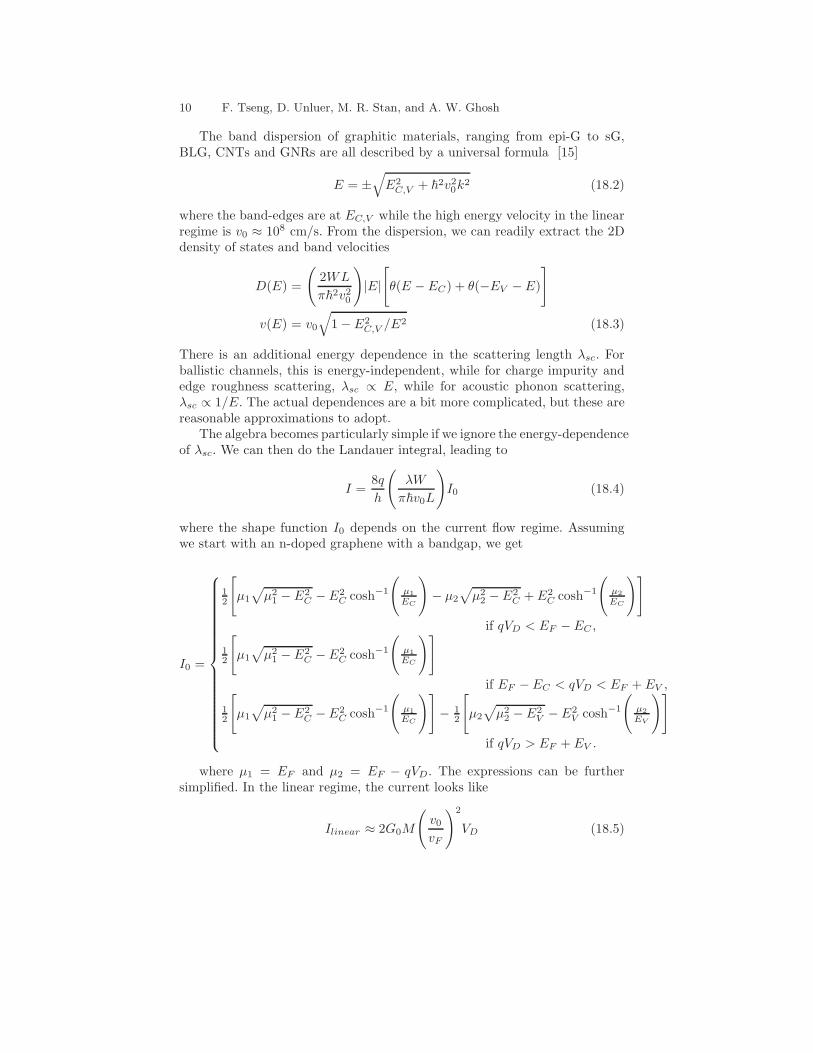
The band dispersion of graphitic materials, ranging from epi-G to sG,BLG, CNTs and GNRs are all described by a universal formula [15]
E = ±√
E2C,V + ~2v20k
2 (18.2)
where the band-edges are at EC,V while the high energy velocity in the linearregime is v0 ≈ 108 cm/s. From the dispersion, we can readily extract the 2Ddensity of states and band velocities
D(E) =
(
2WL
π~2v20
)
|E|[
θ(E − EC) + θ(−EV − E)
]
v(E) = v0
√
1− E2C,V /E
2 (18.3)
There is an additional energy dependence in the scattering length λsc. Forballistic channels, this is energy-independent, while for charge impurity andedge roughness scattering, λsc ∝ E, while for acoustic phonon scattering,λsc ∝ 1/E. The actual dependences are a bit more complicated, but these arereasonable approximations to adopt.
The algebra becomes particularly simple if we ignore the energy-dependenceof λsc. We can then do the Landauer integral, leading to
I =8q
h
(
λW
π~v0L
)
I0 (18.4)
where the shape function I0 depends on the current flow regime. Assumingwe start with an n-doped graphene with a bandgap, we get
I0 =
12
[
µ1
√
µ21 − E2
C − E2C cosh−1
(
µ1
EC
)
− µ2
√
µ22 − E2
C + E2C cosh−1
(
µ2
EC
)]
if qVD < EF − EC ,
12
[
µ1
√
µ21 − E2
C − E2C cosh−1
(
µ1
EC
)]
if EF − EC < qVD < EF + EV ,
12
[
µ1
√
µ21 − E2
C − E2C cosh−1
(
µ1
EC
)]
− 12
[
µ2
√
µ22 − E2
V − E2V cosh−1
(
µ2
EV
)]
if qVD > EF + EV .
where µ1 = EF and µ2 = EF − qVD. The expressions can be furthersimplified. In the linear regime, the current looks like
Ilinear ≈ 2G0M
(
v0vF
)2
VD (18.5)

18 Graphene Nanoribbons: from chemistry to circuits 11
Energy
x
qVDS
0.0 0.5 1.0 1.5 2.0 2.50
0.2
0.4
0.6
0.8
I DS
(m
A)
VDS(V)
Dirac point :
αVG
Band−to−band tunneling
Fig. 18.7. A typical I-V output shows how the I-V tends to saturate at the Diracpoint even without a bandgap. The shift in the Dirac point indicates the Laplacepotential drop along the channel, eventually leading to band-to-band tunneling.
where G0 = q2/h, the number of modes M ≈ 2W/(λF /2), and the Fermivelocity vF = v0
√
1− E2C/E
2F . The saturation current
Isat ≈ 4G0M
(
EF
2q
)
(18.6)
while the band-to-band tunneling current at high bias varies quadratically as
IBTB ≈ 4G0M
(
v0vF
)
VD
(
qVD
2EF
)
(18.7)
Fig. 18.7 shows typical I-Vs based on the above formula. These resultsagree with more involved, atomistic models for EHT coupled with non-equilibrium Green’s function based simulations [16]. The current shows apoint of inflection at the Dirac point, which is shifted by the gate bias(bandgaps would give more extended saturating regions, as we will see forour three terminal I-Vs later on). The subsequent rise in current is indicativeof band-to-band tunneling. Furthermore, a prominent I-V asymmetry, con-sistent with experiments on SiC, can be engineered into our I-Vs (Fig. 18.8)readily by shifting the Fermi energy to simulate a charge transfer ‘doping [17]’of 470meV through substrate impurities, back-bonding and/or charge puddleformation with SiC substrates. A mean-free-path(λsc) that varied inverselywith gate voltage was implemented in the left figure in Fig. 18.8. For n-typeconduction λsc ranged between 18nm to 40nm and 20nm to 31nm for p-type.Typically we would expect at least 100nm for low bias conductance and downto 10nm as the biasing approaches the saturation and band-to-band tunnelingregions. Chosen λsc represent an average scattering length for the different re-gions. A more accurate model for scattering is necessary and will be developedin future works. In contrast, SiO2 seems to dope the sheets minimally and the

12 F. Tseng, D. Unluer, M. R. Stan, and A. W. Ghosh
−5 0 50
2
4
6
8
10
12
Vds
(V)
I ds (
mA
)
Fig. 18.8. (Left) Theoretical and (Right) experimental I-Vs for graphene. Thecalculations on the left assume a ‘doping’ of the sheet by a charge density that shiftsthe K-point relative to neutrality. We also assume an inverse relation between thescattering length λsc and the applied voltage on the n-side, consistent with scatteringby charge puddles associated with the above doping charge. The data on the rightare for graphene on SiC, where charge puddles and/or back-bonding are expectedto transfer a net charge density to the sheet [18].
measured I-Vs show the expected symmetry between the electron and holeconducting sectors.
From the low-bias I-Vs, we can now extract the conductanceG = Ilinear/VD,thence the sheet conductance σs using G = σsW/L, and finally the mobilityµs using σs = qnsµs, where ns is the sheet charge density related to the Fermiwavevector as kF =
√πns. Let us focus on the mobility first, keeping in mind
that the effective mass m∗ in GNRs is energy-dependent.
18.2.2. Low bias mobility-bandgap tradeoffs: asymptotic bandconstraints
Graphene’s linear dispersion is known for contributing to an ultra-high mo-bility, but often overlooked is its origin in the low bandgap that ultimatelyhampers its ON-OFF ratio as an electronic switch. The carrier velocity(v = 1/~dE/dk) fundamentally saturates to v0 = 3a0t/2~ ∼ 108cm/s, whichforces its high energy bandstructure to a linear form regardless of bandgapsize. Regardless of the mechanism of bandgap opening, or the particularprogeny of graphene that we are looking at (epi-G, sG, CNT, GNR or BLG),the bandstructures are always writeable as E(k) ≈ ±
√
(EG/2)2 + (~v0k)2 [2].Such an intimate relation between bandgap and dispersion connecting ulti-mately to its conduction/valence band effective masses (as opposed to mid-gaptunneling effective mass) is unique in materials science.
An extended bandgap constrained by the high energy velocity saturationlocalizes carriers, which shows up as a decrease in curvature at the band edges.

18 Graphene Nanoribbons: from chemistry to circuits 13
Bandgap (eV)0.0 0.5 1.0 1.5 2.0
10–4
10–3
10–2
10–1
100
m0*
/ m0
BMGGNRCNTother semiconductors
InSb els
InSb holesGe holes
Ge els
Si els
Si holesGaAs holes
GaAs els
–0.2 0.0 0.2–2
–1
0
1
2
k
Ene
rgy(
eV)
Fig. 18.9. Scaling of graphite effective masses shows that increasing the bandgapincreases the mass m∗ = pF/vF due to the decrease in average curvature arisingfrom a pinning of the E-k at high energy values [19].
It is easy to show from the above dispersion that the effective mass at eachband-edge satisfies
m∗0 = EG/v
20 (18.8)
indicating that the kinetic energy gained by the electrons and holes uponbandgap opening is taken ultimately from the corresponding crystal potential(Fig. 18.9).
For transport considerations corresponding to high bias electrons andholes, we need to generalize the concept of effective mass to points awayfrom the band-bottom, using m∗ = p/v = ~k/[1/~(∂E/∂k)]. This expressionreduces to the usual dependence on curvature near the band-bottoms uponusing L’Hospital’s rule with k → 0. In other words, effective mass and carriervelocity must be treated as energy dependent variables instead of materialspecific constants. From here, we can then extract the mobility µ = qλsc/p,where carrier momentum p = ~k and λsc is the mean-free-path, related byλsc = π/2(vF τ). From the band dispersion or E versus k relation we definethe Fermi wavevector as:
kF =
√
E2F − E2
gap/4
~v0(18.9)
=√πnS . (18.10)
where Egap/2+αGqVG marks the position of the Fermi level (EF ) relative tothe Dirac-point and nS is the electron density. Relating Eqs. 18.9 and 18.10,we can express a voltage and bandgap dependent electron density to determinethe mobility
µ =qτ
m∗=
qλsc
m∗v=
qλsc
~kF(18.11)
It is thus clear that the mobility depends on the value of kF . As we varythe bandgap of graphitic systems (epi-G, BLG, s-G, or GNR), the variation

14 F. Tseng, D. Unluer, M. R. Stan, and A. W. Ghosh
in kF (equivalently, EF ) depends on what parameters are being held constantin the process. To start, let us assume the scattering length λ is independentof energy, so that we’re effectively working in the ballistic limit. At this point,we can assume the electron density ns is constant while the bandgap is beingopened, so that kF is constant and the mobility does not change. However,possibly a more suitable metric is the gate overdrive VG−VT , which ultimatelydetermines the charge density too using ns = CG(VG − VT ), where C−1
G =C−1
ox + C−1Q involves both oxide and quantum capacitances. In the limit of
small density of states (CQ ≪ Cox) at smaller bandgaps, the gate overdrive isthe quantity that is controlled externally, and this changes ns as the quantumcapacitance proportional to density of states increases with energy. We thenget
nS =αGqVG(αGqVG + Egap)
Lπ~2v20(18.12)
µ =qλ
~√πnS(αGqVG, Egap)
(18.13)
where the gate transfer factor is αG = Cox/CΣ and CΣ is the equivalentcapacitance of a three-terminal device including its quantum capacitance. Thefundamental mean-free-path (λsc) can be approximated semiclassically from
the conductance σs = q2D(EF )D ≈ 2q2
h{λsckF } with kF defined in Eq. 18.10
and D being the diffusion constant. Single layer graphene (SLG) can have λsc
on the order of microns In addition to λsc, a more complete of mean-free-path (λ) from Eq. 18.13 would include scattering due to charged impurities,roughness, and possible phonons from interfacial materials given that phononsnative to graphene are inherently suppressed, (1/λ = 1/λsc + 1/λimpurities +1/λrough + 1/λph).
0.0 0.5 1.0 1.5 2.0102
103
104
105
106
107
Bandgap(eV)
µ (c
m2/
Vs)
ns=4x1010cm-2 λ=1.2µmns=2x1011cm-2 λ=1.2µmns=4x1010cm-2 λ=0.1µmother semiconductors
InSb els
InSb holes
Ge els
Ge holes Si els
Si holes
GaAs els
GaAs holes
InP els
InP holes
230,000 cm2
/ Vs
0.0 0.5 1.0 1.5 2.0102
103
104
105
106
107
Bandgap (eV)
µ (c
m2 /
Vs)
SLG λ=1.0µmBLG λ=1.0µmCNT λ=1.0µmGNR λ=1.0µmsGNR σ = 5% λ=1.0µm
0.0 0.1 0.2104
105
106
GNR vs sGNR(5%)
Fig. 18.10. Decrease in mobility (for fixed gate overdrive) between various graphiticmaterials as well as various electron densities
For a fixed gate overdrive, the mobility even for a ballistic device decreaseswith bandgap, primarily due to the asymptotic constraint that pins the band

18 Graphene Nanoribbons: from chemistry to circuits 15
structure to a high energy linear dispersion. We emphasize that this trade-off arises independent of any reduction in scattering length λsc through the
bandgap opening process. The low effective mass of graphene arose from itssharp conical bandstructure in the first place, so that opening a bandgapwithout removing the higher energy conical dispersion invariably makes thecarriers heavier.
With respect to digital switching applications, the importance of the abovetrade-off cannot be overstated. The mobility ultimately determines the switch-ing speed through the ON current, while the bandgap relates to the ON-OFFratio. For cascaded devices, it is also worth emphasizing that the ON-OFFratio needs to be computed at high bias, as the drain and gate terminals inregular CMOS like cascaded geometries are connected to the same supplyvoltage. Increasing the ON-OFF ratio by increasing the bandgap is predictedthereby to reduce the switching speed. We must therefore evaluate GNRs onthis entire µ − EG curve rather than at an isolated point on this 2D plot.Eq. 18.13 elegantly relates Egap and µ for various λ’s. Analyzing the threeparameters Egap −µ−λ simultaneously allows us to project the performanceof graphene derivatives and compare against other common semiconductorsas seen in Fig. 18.10.
18.3. The third level – active three-terminal electronics
We now move outward to the next circle on the Y-chart, towards three termi-nal active electronic devices. Our main focus will be on a class of patterneddevice-interconnect hybrids, where we see certain notable advantages mainlyon the electrostatics and the contact barriers, but challenges with the smallbandgap show up as band-to-band tunneling and modest ON-OFF ratio.
18.3.1. Wide Narrow Wide (WNW) - All graphene devices
The analyses from the previous sections set the platform for evaluating theI-V characteristics of GNR devices in presence of a third gate terminal. Ourlesson from section 18.1 indicated that the GNR metallicity is primarily setby its ribbon width, showing that one might be able to monolithically patterna wide-narrow-wide all graphene device that flows seamlessly from metallicchannels to semiconducting interconnects. Experiments have in fact shown theability to carve out GNRs using either chemistry or nanoparticle mobilitiesthat snip the sheets almost perfectly along their C-C bonds. GNRs as thin as1 nm with perfect edges have been manufactured chemically [20]. It is thusinteresting to query what the device level advantages of such a monolithicallypatterned GNR would be. We will later discuss the circuit level ramifications.
The structure of an imagined WNW graphene nanoribbon field-effect tran-sistor (GNRFET) is shown in Fig. 18.11. The wide regions are metallic andthe narrow ones semiconducting. There are planar gates both at the top and

16 F. Tseng, D. Unluer, M. R. Stan, and A. W. Ghosh
Fig. 18.11. WNW dual gated all graphene device, showing local E − ks (top), topview (center) and side view (bottom) with the device parameters listed.
the bottom, the top ones for gating and the bottom ones for electrostatic‘doping’ (see figure later for inverters). Let us first discuss how we simulatethe I-V of one of these WNW devices.
18.3.2. Solving quantum transport and electrostatic equations
The calculations we will show couples a suitable bandstructure/density ofstates for the graphene channel with full 3D Poisson’s equation for the elec-trostatics and the Non-Equilibrium Green’s Function (NEGF) formulationfor quantum transport [15]. The wider contact regions are captured recur-sively by computing their surface Green’s functions g1,2(E). The correspond-
ing energy-dependent self-energy matrices Σ1,2(E) = τ1,2 g1,2 τ†1,2 project the
contact states onto the channel subspace, where the τ matrices capture thebonding between the contact and channel regions. In order to capture theinterfacial chemistry properly, we extend the device a couple of layers into thewider regions and calculated its Hamiltonian H matrix. The Coulomb matrixU is computed using the method-of-moments, described below [21].
From the above matrices, the retarded Green’s function G = (ES −H −U − Σ1 − Σ2)
−1 is computed, and thence the charge density matrix ρ =∫dE GΣinG†/2π, whose trace gives us the total charge. Σin = (Γ1f1 +Γ2f2)
in the simple limit where the only scattering arises at the contact channelinterface. In the previous equation, Γ1,2 = i(Σ1,2 − Σ†
1,2) give the contactbroadenings (the matrix analogues of the injection rates γ1,2 introduced insection 18.2.1), while f1,2(E) = 1/[1 + e(E−µ1,2)/kBT ] represent the contact

18 Graphene Nanoribbons: from chemistry to circuits 17
Fermi-Dirac distributions, with µ1,2 being the bias-separated electrochemicalpotentials or quasi-Fermi energies in the contacts [16]. The charge densitymatrix is then used to recompute the Coulomb matrix U self-consistentlythrough Poisson’s equation. Finally, the converged Green’s function is used tocompute the current I = (2q/h)
∫dE T (E)[f1(E) − f2(E)], where the trans-
mission T (E) = trace(Γ1GΓ2G†) [15].
Let us now get into a few details on the 3D Poisson equation we solve,using the method of moments (MOM) numerically. MOM captures the channelpotential by setting up grid points on the individual device atoms with aspecific charge density δnD, and on the contact atoms with a specific appliedvoltage φC [21]. Using the notations ‘C’ for Contact and ‘D’ for Device, weget
φd = (UdCU−1CC)φC
︸ ︷︷ ︸
Laplace
+ (Udd − UdCU−1CCUCd)
︸ ︷︷ ︸
Single Electron Charging Energy
∆nd (18.14)
where we imply vector notations for the potentials φ and matrix notations forthe Coulomb kernels U . ∆nd is calculated relative to its neutrality value N0 bytracing over ρ above, while N0 is calculated analogously, while grounding allthe contact potentials (this would depend on the workfunction of the contacts,as in MOS electrostatics). The matrix elements in U need to be computed withthe correct dielectric constants. Let us describe it in the simpler case with adielectric constant κ for the top gate and a dielectric constant unity for thebottom (trivially generalized to multiple dielectrics). Using the method ofimages,
U(r1, r2) =q
4πǫ0ǫ1
[1
|r1 − r2|−(ǫ2 − ǫ1ǫ2 + ǫ1
)1
|r1 − r′2|
]
(in the same medium)
=q
2πǫ0(ǫ1 + ǫ2)|r1 − r2|(in different media) (18.15)
where r′2 is the image of the charge at r2 [22] [23]. A tricky point is to avoid
the infinities at the onsite locations, for instance, when x1 = x2 and y1 = y2.We can avoid these using the Mataga-Nishimoto approximation, where we re-place terms like 1/|r1 − r2| with an atomistic correction 1/
√
|r1 − r2|2 + a2,with the cut off parameter a adjusted to represent the correct onsite Coulomb(Hubbard) charging energy given by the difference between the atomic ion-ization energy and the electron affinity [24].
Let us now discuss the observed electrostatic characteristics in the WNWdevice, which explains the geometric advantages of this particular structure.
18.3.3. Improved electrostatics in 2-D
We simulate a device patterned monolithically from a two-dimensional sheetof graphene with a wide dilution of widths from the source and drain contacts

18 F. Tseng, D. Unluer, M. R. Stan, and A. W. Ghosh
Fig. 18.12. (Left) The two-terminal potential shows the vanishing fields near thechannel, implying the superior gate control and the improved short-channel effectswith the 2D contacts. (Right) The 3D potential shows the non-linear flat potentialin the middle of the channel.
to the active channel region. Simulated WNW (35-7-35) GNRFETs composeof (7,0) armchair graphene nanoribbon (GNR) narrow regions for the channeland (35,0) armchair GNR regions for the contact and interconnect regions. Ametallic gate is placed on top of the channel region, while a wide groundedsubstrate is placed at the bottom of the channel. For calibration with theconventional CMOS technologies, the unique two-dimensional (2D) contactsof the GNRFET are replaced with 3D bulk metal contacts (whose surfaces actas parallel plate capacitors) for the same device, gate, and dielectric geometry.
A particular advantage of the WNW structure is the low capacitance of the2D source drain contacts [25]. In a conventional MOSFET, the gate electrodeneeds to compete electrostatically with the source and drain for control of thechannel charge. Indeed, a majority of developments in transistor technologyover the last few decades have concentrated on making the field lines gatecontrolled rather than source/drain controlled. This is becoming harder withaggressive size scaling. The 2D source and drain contacts with a top gatemakes the S/D capacitances lower, as they can only influence the channelthrough their fringing fields. Note that a 2D side gate geometry, as advocatedin many device designs, would eliminate that electrostatic advantage, as thegate needs to compete with the S/D electrodes.
As the channel length gets shorter with the aggressively scaled technolo-gies, the 3D contacts start to influence the channel potential as their surfacesact as parallel capacitor plates flanked by the insulator at the top and bottom.In the case of the monolithically patterned 2D GNR contacts, the charges onthe contact surfaces are line charges so that the applied source-drain fielddecays into the channel, creating a non-linear channel potential even in the
absence of a gate (Fig. 18.12, left). Moving on to a three-terminal, dually gatedstructure, Fig. 18.12 (right), shows that the gate contact holds the channelpotential flat against the action of the drain, thereby reducing short-channeleffects.

18 Graphene Nanoribbons: from chemistry to circuits 19
Fig. 18.13. Comparison of planar source drain vs 3D source-drain. Denser fieldlines on the channel from the 3D contacts correlate to stronger source coupling andDIBL. For the given material and geometrical parameters listed in Fig. 18.11, theCG/CD ratios are 4.95 and 5.80 respectively. Top and bottom gates were groundedwhile the source was simulated with a potential of 0.3V and conducting channel hada potential of 0.1V
Figs. 18.13, 18.14 show that for the same channel geometry, the top gatewith 2D side contacts has the largest capacitance, followed by the top gatewith 3D side contacts and finally the lowest gate to drain capacitance ratiois obtained when all electrodes are co-planar. The corresponding field linediagrams are also shown in these figures. Note also that in addition to thesource, drain and dual gate electrodes, one needs to worry about the quan-tum capacitances, which are automatically included from our density matrixcalculations that enter Poisson’s equation.
The capacitance ratio can be extracted by plotting the channel transmis-sion (T) for two scenarios: maintaining a constant drain voltage (Vd) whilesweeping gate voltage (Vg) , and analogously, maintaining a constant Vg whilesweeping Vd. Sweeping the Vg creates a larger energy shift in the transmissionof the GNRFET channel than the sweeping of the Vd. From the shifting ratesof these transmissions and the charge density calculations from the MOM, wecan extract the capacitance values of the contacts. With shifts in transmis-sion plots, we once again find that 2D contacts indeed help the gate exercisesuperior control over the channel [25].

20 F. Tseng, D. Unluer, M. R. Stan, and A. W. Ghosh
Fig. 18.14. Comparison of top vs side gate. Denser field lines from the top gateensure better gate control which is reflected by larger gate capacitance. For the givenmaterial and geometrical parameters listed in Fig. 18.11, the CG/CD ratios are 5.80and 3.82 respectively. Gates were biased at 0.4V , while the conducting channel hada potential of 0.1V.
We will now explore the effect of the improved short channel effect on thecomputed I-V characteristics.
18.3.4. Three terminal I-Vs
The computed three terminal I-Vs (Fig. 18.15) show excellent short channeleffects, at least over a small voltage range given by the bandgap. Plottedvs gate voltage, the current shows excellent saturation characteristics with alarge output impedance. Plotted vs gate voltage, the current shows little drainbias dependence (so-called drain induced barrier lowering or DIBL). Takentogether, the curves signify that the device electrostatics in the geometry isnearly ideal, making the outputs relatively robust with process variations. Itis interesting to note that instead of enhancing the gate capacitance as inregular CMOS devices, the trick in WNW devices has been to reduce thesource and drain capacitances in comparison.
The simulations results of the model in the Fig. 18.15 demonstrate a Sub-threshold Swing (SS) of 84.3 mV/dec and a Drain-Induced Barrier Lowering(DIBL) of 24 mV/V. We note that unless otherwise specified all simulationsrefer to material and geometrical parameters shown in Fig. 18.11 The valueof the DIBL and the SS can be further improved by increasing the length ofthe channel (currently 1:8.6 ratio of HfO2 thickness to channel length). Thesevalues calculated are better (smaller) than the estimated values of DIBL =122 mV/V and the SS = 90 mV/dec for the double gate, 10 nm scaled SiMOSFETs [26]. Also in addition to showing improved short-channel effects,

18 Graphene Nanoribbons: from chemistry to circuits 21
the GNRFET structure with the 2D contacts also shows controlled switchingbehavior. The on-current (Ion) of the system equals to 2670.62 A/µm withthe off-current (Ioff) set at 4.07 A/µm; thus giving a Ion/Ioff ratio of 656.The ON-OFF ratio, however, ends up being modest, and is a critical challengein GNRFETs, especially in the light of its seemingly inverse relation with thecharge mobility (section 18.2.2).
0 0.2 0.40
1000
2000
3000Vds Sweep
Vds(V)
Id(
µA/
µm)
Vgs=0.4VVgs=0.3VVgs=0.2VVgs=0.1VVgs=0.0V
0 0.2 0.4
102
Vgs Sweep Log Scale
Vgs(V)
Id(
µA/
µm)
Vds=0.4VVds=0.3VVds=0.2VVds=0.1V
Fig. 18.15. I-V curves for a n-type GNRFET confined to create a large bandgap(in this case, a (7,0) armchair GNR with a bandgap nearly 1 eV). Such an extremegeometry postpones the onset of band-to-band tunneling. More importantly, thepoint of the I-V is to show the effect of better electrostatics which is independent ofbandgap issues – resulting in a high current saturation, low DIBL and SS.
With the scaling of the channel length, the short-channel effects startedto have a huge influence on the device parameters such as the DIBL and SS.As the channel lengths get shorter, the DIBL and SS of the device increasesdue to the Cg/Cd ratio of decreasing with length. The line charges with the2D contacts endow the gate with more control over the channel and interfacestates compared to the 3D contacts by lowering the drain capacitance.
18.3.5. Pinning vs. Quasi-Ohmic contacts
In today’s semiconductors, Ohmic contacts are a desired to help achieve linearand asymmetric I-V characteristics. The potential profile inside the channelcan be influenced by increasing the drain-source voltage (Vds) or the gatevoltage (Vgs). For carbon nanotubes, this has been a particular challenge,as the metal carbon bonds at the ends have predominantly created Schot-tky barriers [27]. In our WNW geometries, since the bulk metal contactsare relegated to the ends of the device array, the bonding configuration nearthe wide-narrow interfaces are controlled by C-C covalent bonding. As oursimulations show, this seems to promote a quasi-Ohmic behavior. The bet-ter bonding increases the decay lengths of the corresponding metal-inducedgap states (MIGS) entering from the wide regions. The partial delocalizationreduces the single-electron charging energy (that enters through our MOM

22 F. Tseng, D. Unluer, M. R. Stan, and A. W. Ghosh
treatment), thus making it harder for the contact regions to pin the Fermienergy and reducing the effectiveness of the Schottky barrier.
Schottky barrier FETs behave qualitatively different from MOSFETs Inthe latter, an applied gate bias reduces the channel potential and controlsthe thermionic emission over the voltage-dependent interfacial barrier. In theformer, the gate reduces the thickness of the Schottky barrier and controls thetunneling of electrons through a voltage-independent, pinned barrier height.The question is what the potential profile looks like in the channel, andwhether the contact MIGS are effective in pinning this potential adequately.
As seen in the Fig. 18.16, the lowering of the potential throughout theentire graphene channel region with applied gate bias is a characteristic of theregular ohmic contact FETs rather than the Schottky barrier FETs, whosepotentials would otherwise be pinned to the midgap by the charging of theinterfacial states [28].
Fig. 18.16. At Vds = 0.0V and Vds = 1.0V, variation of channel potential withdifferent gate voltages shows no barrier pinning at the contacts, implying Ohmiccontacts.
The MIGS due to the tail ends of the metal states in the contacts, leakin the semiconductor. Even with this 2D contact geometry, the MIGS will bepresent because of the contact-channel interfaces [25]. OurWNW all-graphenestructure can filter these quickly decaying states, resulting in no significantcontribution to the electron transmission. In the case of our device with thechannel length of 8.66 nm, the MIGS do not travel all the way from sourceto the drain, but only extend approximately 0.7 nm into the semiconductingchannel (Note a typo in one of our earlier papers, where we wrongly quotedthis as 0.07 nm) [25]. The decay length of these MIGS can be calculated byplotting the wavefunction of the channel electrons at specific energies, as wellas by evaluating the complex E-k diagram. The intensity of these MIGS at agiven distance x can be calculated by using the equation I0*e
(−x/2λ), whereI0 is the intensity of MIGS at the interface and λ is the decay length.
18 Graphene Nanoribbons: from chemistry to circuits 23
Note that issues similar to those discussed here have been discussed inthe context of pentacene molecules with CNT contacts. While CNTs wouldoffer even better 1D electrostatic gains, a trade-off arises with the increasingseries resistance in CNTs due to a paucity of modes. For GNR source/drainanalogously, we will need to imagine wide blocks simultaneously contactingmany GNR devices, so that the contact resistance is minimized by extendingits width.
We now have all the tools to compute three-terminal I-Vs in graphiticstructures, doing full justice to the complex electrostatics. Let us now see howthis influences the circuit level performance metrics of GNRs.
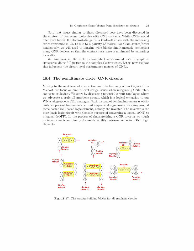
18.4. The penultimate circle: GNR circuits
Moving to the next level of abstraction and the last rung of our Gajski-KuhnY-chart, we focus on circuit level design issues when integrating GNR inter-connects or devices. We start by discussing potential circuit topologies wherewe advocate a truly all graphene circuit, which is a logical extension to ourWNW all graphene FET analogue. Next, instead of delving into an array of cir-cuits we present fundamental circuit response design issues revolving aroundsome basic GNR based logic element, namely the inverter. The inverter is themost basic logic circuit with the sole purpose of converting a logical 1(ON) toa logical 0(OFF). In the process of characterizing a GNR inverter we touchon interconnects and finally discuss drivability between connected GNR logicelements.
Fig. 18.17. The various building blocks for all graphene circuits
24 F. Tseng, D. Unluer, M. R. Stan, and A. W. Ghosh
18.4.1. Geometry of an all graphene circuit
An attractive feature of graphene for device engineers is its planarity, whichstems from its sp2 chemical bond hybridization. Graphene’s atomic flatnessis compatible with existing lithographic device fabrication techniques estab-lished for CMOS. Furthermore, exploiting how chirality in graphene influenceselectronic properties we present an array of building blocks for all graphenecircuits (Fig. 18.17). In the previous circle on our Y-chart we explored an allarmchair GNRFET.
Circuit level enhancements start at the device level. Two important deviceperformance metrics for digital circuit performance are ON-OFF current ratioand intrinsic gate propagation delay. GNRFET ON current scales proportion-ally with width, while the OFF current goes as eEg/kT or ec/WkT , where Wis the width. To achieve manageable OFF currents for digital applications,GNR widths must be scaled within the sub-10nm regime to avoid increasedin static power dissipation and poor ON-OFF ratio. However GNR scalinghas little influence on propagation delay.
Propagation delay is defined as CINVdd/ION , where CIN is the intrinsiccapacitance, Vdd is the supply voltage and ION is the saturating ON currentat Vgs=Vdd. Increasing channel width increases ION by shifting the thresholdvoltage and would seemingly improve delay at the expense of an exponentiallyincreasing OFF current. However CIN = (1/Cox + 1/CQ)
−1 also scales withwidth, thereby removing any improvement in propagation delay from simplescaling of graphene. From the perspective of a single GNR device there arenot many options to improving the propagation delay. However a more usefulcontext to address this issue would be on the circuit level where we havemultiple logic elements.
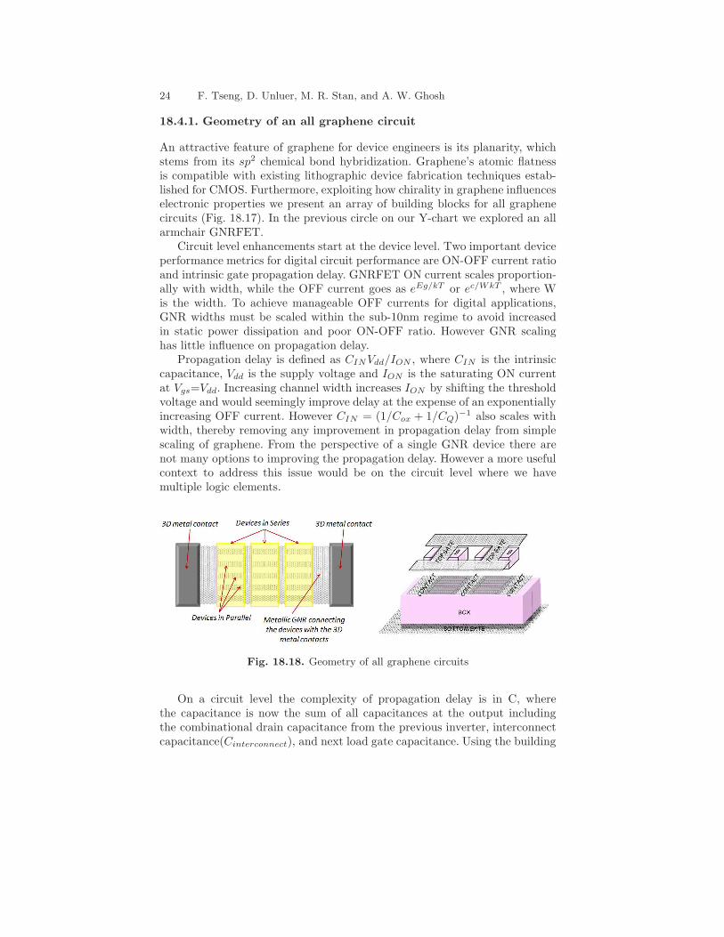
Fig. 18.18. Geometry of all graphene circuits
On a circuit level the complexity of propagation delay is in C, wherethe capacitance is now the sum of all capacitances at the output includingthe combinational drain capacitance from the previous inverter, interconnectcapacitance(Cinterconnect), and next load gate capacitance. Using the building

18 Graphene Nanoribbons: from chemistry to circuits 25
blocks in Fig. 18.17 we present an all graphene circuit shown in Fig. 18.18, withcascaded GNRs in parallel on a semiconducting substrate with separate splitgates for electrostatic doping the regions n and p-type. The cascaded GNRscould be separated by a high-k dielectric or even boron nitride in hexago-nal lattice, which has the advantage of being atomically flat and absence ofdangling bonds [17] makes it less likely to carry adsorbents that could de-grade the device. The advantage here is that ON-OFF ratio is held constant,while the increased ON current and capacitance which scale with N numberof cascaded GNRs dilutes the parasitic interconnect capacitance and improvespropagation delay and circuit performance.
Good quality graphene sheets have been made viable by current advance-ments in wafer-scale and pattern transfer techniques [18, 29]. However fullrealization of an all graphene circuit with various GNR interconnects and de-vices rely on the ability to pattern GNRs to narrow enough widths to producea sizable bandgaps. Planar lithographic techniques are prone to edge rough-ness, while various chemical methods have had the most success in creatingchemically precise GNR edges, but their applicability to scalable device levelprocesses remain to be seen [7] [30] [31] [32]. While roughness helps to makeGNRs insensitive to chirality, we need further simulations to see how atomicfluctuations in the widths influence the corresponding threshold voltages andON/OFF currents, an issue critical for the overall reliability of GNR circuits.
18.4.2. Compact Model Equations
To simulate the performance of such a circuit, let us first outline a compactmodel. This will require us to outline (a) an equation for the bandstructurethat includes effects due to edge strain and roughness, (b) an equation for thescattering length that depends on the phonon spectrum and edge roughness,(c) equations for the 2D electrostatics due to the source and drain contacts,and (d) the resulting I-Vs obtained by integrating the transmission over therelevant energy window.
To recap, the bandstructure of GNRs, including edge strain, can be written
in a tight-binding form as E = ±√
E2C,V + ~2v20k
2. Specific expressions for
EC,V and v0 for variously strained graphitic materials exist in Ref. [9].The next term is the scattering λsc, which is related to the scattering time
through an angle averaged geometrical factor and the overall Fermi velocity.The scattering time is extracted from Fermi’s Golden Rule. For short rangescattering by edge roughness and phonons, τsc ∝ 1/|E|, while for long rangedunscreened Coulomb scattering, τsc ∝ |E|. Explicit expressions exist in theliterature [33] [34].
The tricky part that does not exist in the literature are the electrostaticcapacitances associated with the 2D electrostatics from the planar source anddrain contacts, competing with the top and bottom gates through their in-dividual dielectrics. We are in the process of extracting formulae based on

26 F. Tseng, D. Unluer, M. R. Stan, and A. W. Ghosh
knowledge of planar micro-strip line electrostatics, with geometrical factorscalibrated with our numerical MOM solutions for a variety of geometries [25].
Once we have the electrostatic, band and scattering parameters, we canthen use Eq. 18.1 to extract the I-Vs. For energy-independent λsc, this wasalready shown earlier. We will generalize it to various scattering configurationsin our future work.
We thus have a comprehensive compact model that captures the chemistryand bandstructure, scattering, electrostatic and transport parameters neededfor our circuit simulations. We will report one example here, and report furtherresults in our subsequent publications.
18.4.3. Digital circuits:
Static complementary CMOS gates utilize pull-up (PUN) and pull-down(PDN) networks to achieve low power dissipation and large noise margin inlogic circuits such as the inverter, NAND, and NOR gates. CMOS logic cir-cuits are composed of some series and parallel combinations of n and p-typeFETs. An inverter illustrated in Fig. 18.19 is the simplest logic element andthe focus of this section of the review.
Fig. 18.19. GNR inverter geometry and voltage transfer curve. This inverter designuses the WNW (metal-semiconductor-metal) all graphene structure for pull-up andpull-down networks. In this design CNT interconnects make direct contact with de-vice level graphene. CNT/graphene interface has been experimentally demonstratedby Fujitsu Laboratories Ltd [35,36].
When the input into the common gate is Vin=0 the p-type FET (PUN)is active while the n-type FET (PDN) is cut-off, hence the circuit will pullthe output voltage up toward the supply voltage (Vdd) or high, Vout=1.

18 Graphene Nanoribbons: from chemistry to circuits 27
Likewise when Vin=1, n-type FET is active and p-type FET is cut-off pullingthe circuit down toward ground, Vout=0. Usually it is impossible to pull-upor pull-down to exact values of 1 or 0, so threshold voltage and tolerance aredesigned for each circuit to help distinguishing between these two logic levels.Circuit designers allow some tolerance in the voltage levels used to avoidconditions that generate intermediate levels that are undefined. For example,0 to 0.2V on the output can represent logic (0) and 0.3 to 0.5V can show (1),making the 0.2 to 0.3V range invalid, not metastable, since the circuits cannotinstantly change voltage levels.
The voltage-transfer curve (VTC) of an inverter circuit captures the DCor steady-state of specific input versus output voltages and provides a figureof merit for the static behavior of the inverter. VTCs for logic circuits provideinformation on operating logic-levels at the output, noise margins, and gain.Ideally we want the VTC to appear as an inverted step-function, indicatingprecise switching between the on and off stages, but in real devices there is acontinuous transition between on and off states. From the VTC we can extractnoise margin (Fig. 18.20), which provides a measure of circuit reliability andpredictability. Biasing outside the noise margin puts the logic circuit in anunpredictable state. Circuit designers want to maximize the noise margins.
Fig. 18.20. showing the importance of balancing CMOS transistor sizes to achieveequal high and low noise margins(NM). The noise margin is graphically representedby the largest square that fits inside the enclosed space outlined by normal androtated VTCs.
A significant advantage of graphene is its intrinsic electron-hole effective
mass symmetry. In the absence of extrinsic doping a graphene based FET theI-V characteristics for n and p-type conduction would be the symmetric. How-ever, asymmetry can be introduced into the system through charge-transferdoping [17] (e.g. Fig. 18.8) or by contact induced doping [37]. Significantscreening of charge impurities in the substrate should bring Fermi level closerto its intrinsic value at the Dirac or K−point, therefore recovering symmetricn and p-type I-V characteristics. On a circuit level this symmetry means the
response of PUN and PDN would be equal and opposite, which is important
for circuit reliability, and not to mention ease of circuit design. In conven-tional Si-CMOS logic circuits, the asymmetry in the electron-hole effective

28 F. Tseng, D. Unluer, M. R. Stan, and A. W. Ghosh
mass is compensated by scaling the physical width of the p-type FETs in thePUN so the I-Vs are equal and opposite with the PDN. Graphene’s naturalelectron-hole symmetry would allow circuit designers to bypass this designissue.
A major impediment to GNR based logic circuits is its narrow bandgap( 6 200meV ), as the device elements in the PUN and PDN are prone tosub-threshold leakage from band-to-band tunneling. The two-fold effect on anGNRFET-based inverter where the channel has a narrow bandgap is demon-strated in Fig. 18.21. The first effect is a large voltage swing of approximately0.4V. The second effect is a significantly diminished noise margin. Band-to-band tunneling in narrow bandgap GNRFETs prevents either the PUN or thePDN from completely cutting off when its complement network is active.
0 0.2 0.4 0.6 0.8 10
1
2
3
4
5
Vout(V)
In,p(mA)
Narrow Bandgap GNR
pGNR nGNR
0 0.2 0.4 0.6 0.8 10
0.2
0.4
0.6
0.8
1
Vout(V)
Vin(V)
Voltage Transfer Curve
GNRNarrow BandgapCMOSLarge Bandgap
Fig. 18.21. Comparison of VTC curves for narrow bandgap GNR and 45nm CMOSTechnology. Narrow bandgap GNRFETs will be more susceptible to noise thanCMOS due to smaller noise margins.
Fig. 18.19 shows the physical layout of a functional graphene inverter com-posed of WNW P-type and N-type GNR device arrays and the voltage transfercurve. The inverter voltage-transfer curve and gain can be calculated readilyfrom the current-voltage characteristics. As expected the gain of the device de-termined by the electrostatics, geometrical parameters, and mobilities whichultimately determine the P and N-type GNR transconductances. The VTCabove with gain of 4 is derived from the I-V shown in Fig. 18.19 for the 8.66nmdevice by using the methodology described in detail in [38]. These I-Vs gener-ated in SPICE can be used to simulate other complex layouts such as NANDor NOR gates shown in Fig. 18.22 (The results of these logic gates will bereported in future publications).
Propagation delay can be measured by pulsing the input voltage between0 and 1 and observing the output transient response. The transit time for aGNRFET is approximately L/v, where L is the length of the channel and v isan energy dependent velocity defined in Eq. 18.3. Intrinsic and extrinsic device

18 Graphene Nanoribbons: from chemistry to circuits 29
level scattering mechanics could also influence transit time. However, a cascadeof inverters or some other logic elements in series, the load capacitance betweeneach logic stage typically dominated by Cinterconnect would be responsible forthe majority of the delay. The GNR circuit layout we presented earlier andshow in Fig. 18.18 addresses the parasitic capacitances by lowering delay andincreasing performance.
Beyond individual logical elements (ie., inverter, NAND, NOR), an impor-tant CMOS circuit design parameter is fan-out, which estimates the numberof logic stages or CMOS gates that can be consecutively driven before signalattenuation is no longer tolerable. Past the maximum fan-out a repeater oramplifier is necessary to drive subsequent logic stages in a circuit. The maxi-mum fan-out scales proportionally with propagation delay; therefore circuitsdesigned for low frequency applications have a larger maximum fan-out com-pared to circuits designed for higher frequency applications. If graphene is toindeed follow the MOSFET and CMOS paradigm fan-out would be importantcircuit design trade-off to consider and a topic we will discuss in an upcomingwork.
18.4.4. Physical domain issues: monolithic device-interconnectstructures
The bane of many CNT-based circuit ideas is the degradation due to thedominant aspect of the Schottky contacts between the devices and intercon-nect. Luckily, GNR circuits can avoid this problem by using the same sheetof graphene for both active devices and interconnect, as seen in Fig. 18.22
Thus, for such monolithic GNR device/interconnect structures with Ohmiccontacts, the behavior can be close to the ideal device predicted by simula-tions. Of course, contacts to metal are still required, but at a coarser gran-ularity, thus the expected degradation in performance will be proportionallysmaller. Contacts to metal are necessary for several reasons; first, the FETgates and drain/source electrodes cannot share the same graphene sheet, soconnecting the output (drain) of a device to the input (gate) of the next willrequire a contact, second, topological requirements for connecting complexcircuits can rarely be mapped to a planar graph, and non-planar graphs im-plicitly require more than one layer of interconnect, thus contacts, and for areally large circuit a large number of interconnect layers (∼ 10 for a modernCMOS circuit).
18.5. Conclusions
The future of microelectronics relies on continually scaling the critical dimen-sions of bulk CMOS technologies. The semiconductor industry faces seriouschallenges in this respect, due to a host of technical and economic constraints.One way to mitigate this is to use novel architectures, combining inherently

30 F. Tseng, D. Unluer, M. R. Stan, and A. W. Ghosh
Fig. 18.22. GNR NAND layouts with electrostatic doped back-gates and intercon-necting ‘vias’ between multiple levels. CNT/graphene interface has been experimen-tally demonstrated by Fujitsu Laboratories Ltd [35,36].
scalable top-down techniques, such as lithography, with novel bottom-up fab-rication approaches, such as self-assembly. An alternate way is to look fornovel channel materials beyond silicon - a strong candidate being anothergroup IV element, carbon, graphene being one of its distinguished allotropes.
Until recently, much attention has been focused on CNTs. CNTs havealready demonstrated excellent intrinsic performance, high gain, high carriermobility, high reliability, and are almost ideal devices in themselves [39][40] [41]. Unfortunately, there seem to be no practical, scalable solutions forarranging multiple CNTs on a substrate uniformly with a small pitch, neededto deliver adequate current for fast switching [31] [42]. Neither are thereclear approaches for contacting CNTs to interconnects or to each other at lowimpedance to realize complex circuits using large scale fabrication schemes. Infact, CNTs frequently encounter Schottky barriers at the contacts that controlthe tunneling electrons, hampering their reliability [43].
In contrast, graphene’s planar profile makes it amenable to well-establishedplanar fabrication techniques for silicon CMOS devices. Its mobility can reach

18 Graphene Nanoribbons: from chemistry to circuits 31
up to two orders of magnitude above silicon, and the ability to engineer itsbandgap with width alone points to the feasibility of all-graphene devices thatcan exploit covalent bonding chemistry at the contact and better inherent elec-trostatics to allow more traditional, MOSFET like gate control mechanisms.However its bane seems to be its metallicity. As we saw earlier, grapheneis naturally a zero-band gap semi-metal, and attempts to open a bandgap,such as through strain, quantization or field asymmetries have limited thebandgaps to < 200 mV [20]. In a regular field effect transistor application,such a bandgap translates to an ON-OFF ratio of ∼ 70, inadequate for digitallogic [44]. This seems consistent with experiments on high speed graphenetransistors, which show I-Vs that are essentially quasi-linear. There is a lotof activity also on opening bandgaps in graphene, although it seems that thismay reduce the mobility that made graphene a promising electronic device inthe first place.
Despite the significant challenges, graphene’s high carrier mobility andfast switching speeds make it widely studied. This includes revolutionary ap-plications such as based on charge focusing, graphene spintronics and ex-citonic condensation of pseudospin states [45]. At the same time, there iswide activity on graphene based conventional electronic devices, specifically,RF devices and CMOS switches. It is not clear what the prospects of GNRsare vis-a-vis switching, given its low bandgap and its seemingly fundamentalmobility-bandgap tradeoff. However, as we have argued here, there still area few notable advantages to using graphene geometries, namely, (i) a natu-
ral electron-hole symmetry that helps with inverter design; (ii) its convenient
placement between 1D and 3D, so that it offers distinct electrostatic advan-tages without picking up too much series resistance arising from a paucity ofmodes; (iii) the tunability of its electronic properties primarily by controllingits width. Experiments are still emerging on these fronts, and it remains tobe seen whether one can put these advantages to good use.
In this chapter, we made a first attempt to transverse the Gajski-KuhnY chart adapted to graphene, spanning physical, structural and behavioraldomains for graphene. We ended with monolithic all graphene circuits anddevice/interconnect geometries, ultimately stopping short of the outermostcircle that covers a system level topology and behavior. A key tool developedalong the way was a compact model for GNRs that capture chemical, geo-metric, electronic, electrostatic and transport properties through a set of sim-ple parameterized equations calibrated against a few emerging experiments.Such a Y-chart is the first step towards a holistic approach that we hope willcatapult graphene from the domain of fascinating physics and chemistry totechnologically relevant electronic applications.

32 F. Tseng, D. Unluer, M. R. Stan, and A. W. Ghosh
18.6. Acknowledgements
We would like to thank Keith Williams, Kurt Gaskill, Jeong-Sun Moon andMark Lundstrom for useful discussions. This work was supported by the NSF-NRI, NSF-NIRT and the UVa-FEST grants.
References
1. T. Beierlein, O. Hagenbruch, Taschenbuch Mikroprozessortechnik (Fachbuchver-lag Leipzig, 1999)
2. A.H. Castro Neto, F. Guinea, N.M.R. Peres, K.S. Novoselov, A.K. Geim, Rev.Mod. Phys. 81(1), 109 (2009)
3. Z. Chen, Y.M. Lin, M.J. Rooks, A. P., Physica E: Low-dimensional Systemsand Nanostructures 40(2), 228 (2007). International Symposium on Nanometer-Scale Quantum Physics
4. K. Bolotin, K. Sikes, Z. Jiang, M. Klima, G. Fudenberg, J. Hone, P. Kim,H. Stormer, Solid State Communications 146(9-10), 351 (2008)
5. D. Kienle, J.I. Cerda, A.W. Ghosh, Journal of Applied Physics 100(4), 043714(2006)
6. Y.W. Son, M.L. Cohen, S.G. Louie, Phys. Rev. Lett. 97(21), 216803 (2006)7. M.Y. Han, B. Ozyilmaz, Y. Zhang, P. Kim, Phys. Rev. Lett. 98(20), 206805
(2007)8. X. Li, X. Wang, L. Zhang, S. Lee, H. Dai, Science 319(5867), 1229 (2008)9. D. Gunlycke, C.T. White, Phys. Rev. B 77(11), 115116 (2008)
10. F. Tseng, D. Unluer, K. Holcomb, M.R. Stan, A.W. Ghosh, Applied PhysicsLetters 94(22), 223112 (2009)
11. D. Areshkin, D. Gunlycke, C. White, Nano Letters 7(1), 204 (2007). PMID:17212465
12. Nature Nanotechnology 3, 397 (2008)13. X. Wang, Y. Ouyang, X. Li, H. Wang, J. Guo, H. Dai, Phys. Rev. Lett. 100(20),
206803 (2008)14. D.V. Kosynkin, A.L. Higginbotham, A. Sinitskii, J.R. Lomeda, A. Dimiev, B.K.
Price, J.M. Tour, Nature 458, 872 (2009)15. S. Datta, Quantum Transport: Atom to Transistor (Cambridge University Press,
2005)16. S. Datta, in Electron Devices Meeting, 2002. IEDM ’02. Digest. International
(2002), pp. 703 – 70617. Applied Physics Letters 97(11), 112109 (2010)18. P. First, W.A. deHeer, T. Seyller, C. Berger, J.A. Stroscio, J. Moon, MRS
Bulletin 35 (2010)19. S.M. Sze, K.K. Ng, Physics of Semiconductor Devices (Wiley, 2006)20. Nature 466, 470 (2010)21. S. Ramo, J.R. Whinnery, T. Van Duzer, Field and Wave in Communication
Electronics (Wiley, 1993)22. J. Jackson, Classical Electrodynamics (Wiley, 1975)23. N. Neophytou, J. Guo, M. Lundstorm, in Computational Electronics, 2004.
IWCE-10 2004. Abstracts. 10th International Workshop on (2004), pp. 175 –176

18 Graphene Nanoribbons: from chemistry to circuits 33
24. J.N. Murrell, A.J. Harger, Semi-Empirical SCF MO Theory of Molecules (Wiley,1972)
25. D. Unluer, F. Tseng, A. Ghosh, M. Stan, Nanotechnology, IEEE Transactionson PP(99), 1 (2010)
26. S. Hasan, J. Wang, M. Lundstrom, Solid-State Electronics 48(6), 867 (2004).Silicon On Insulator Technology and Devices
27. J. Guo, A. Javey, H. Dai, M. Lundstrom, in Electron Devices Meeting, 2004.IEDM Technical Digest. IEEE International (2004), pp. 703 – 706
28. F. Leonard, J. Tersoff, Phys. Rev. Lett. 84(20), 4693 (2000)29. Y.M. Lin, C. Dimitrakopoulos, K.A. Jenkins, D.B. Farmer, H.Y. Chiu, A. Grill,
P. Avouris, Science 327(5966), 662 (2010)30. E. Stolyarova, K.T. Rim, S. Ryu, J. Maultzsch, P. Kim, L.E. Brus, T.F. Heinz,
M.S. Hybertsen, G.W. Flynn, in PNAS May 29, 2007 (2007)31. Y. Zhang, A. Chang, J. Cao, Q. Wang, W. Kim, Y. Li, N. Morris, E. Yenilmez,
J. Kong, H. Dai, Applied Physics Letters 79(19), 3155 (2001)32. M.C. Lemme, T.J. Echtermeyer, M. Baus, H. Kurz, IEEE Electron Devices Let.
28, 282 (2007)33. S. R., T.M. Mohiuddin, Charge carrier mobility degradation in graphene shee-
tunder induced strain. ArXiv:1008.4425v334. T. Fang, A. Konar, H. Xing, D. Jena, Phys. Rev. B 78(20), 205403 (2008)35. M. Katagiri, Y. Yamazaki, N. Sakuma, M. Suzuki, T. Sakai, M. Wada, N. Naka-
mura, N. Matsunaga, S. Sato, M. Nihei, Y. Awano, in Interconnect TechnologyConference, 2009. IITC 2009. IEEE International (2009), pp. 44 –46
36. Y. Awano, (The Fullerenes and Nanotubes Research Society, 2008)37. D.B. Farmer, R. Golizadeh-Mojarad, V. Perebeinos, Y.M. Lin, G.S. Tulevski,
J.C. Tsang, P. Avouris, Nano Letters 9(1), 388 (2009)38. J.M. Rabaey, A. Chandrakasan, B. Nikolic, Digital Integrated Circuits - A De-
sign Perspective (2nd Ed) (Prentice Hall, 2003)39. A. Bachtold, P. Hadley, T. Nakanishi, C. Dekker, Science 294(5545), 1317 (2001)40. R. Martel, H.S. Wong, K. Chan, P. Avouris, in Electron Devices Meeting, 2001.
IEDM Technical Digest. International (2001), pp. 7.5.1 –7.5.441. S.J. Tans, A.R.M. Verschueren, C. Dekker, Nature 393, 49 (1998)42. A.M. Cassell, N.R. Franklin, T.W. Tombler, E.M. Chan, J. Han, H. Dai, Journal
of the American Chemical Society 121(34), 7975 (1999)43. J. Guo, S. Datta, M. Lundstrom, Electron Devices, IEEE Transactions on 51(2),
172 (2004)44. G.C. Liang, A.W. Ghosh, M. Paulsson, S. Datta, Phys. Rev. B 69(11), 115302
(2004)45. D. Reddy, L.F. Register, E. Tutuc, A. MacDonald, S.K. Banerjee, in Device
Research Conference, 2009. DRC 2009 (2009), pp. 67 –68