Embed Size (px)
Citation preview
Graphene and other 2-dimensional materials
An innovative toolbox supporting 2D materials research
Materials growthand deposition
Low temperature and ultra low temperature tools
Fabrication Analysis
Characterisation
2DToolbox
UHV Scanning Probe Microscopy and spectroscopy, Atomic Force Microscopy, SEM based nanoanalysis and nanomanipulation

CVD, PECVD and ICPCVD
CVD: Nanofab® 1000 Agile
Plasma Technology’s Nanofab1000Agile delivers high performance growth
of nanomaterials with in-situ catalyst activation and rigorous process control.
• Cold wall design with showerhead based
uniform precursor delivery
• Remote plasma via ICP option
• Vacuum load lock for quick sample exchange
• Excellent temperature uniformity
• Optional liquid/solid source delivery system and heated
gas delivery option
• Variable sample sizes up to maximum 200mm wafers
• Multiple view ports for diagnostics
Chemical Vapour Deposition (CVD) techniques form the
workhorse for research on 2D materials. The flexibility of
this technique allows deposition down to atomic layers as
well as thicker films.
Materials Growth
Vertical Graphene : (a) Cross-sectional SEM image of vertical graphene, scale bar is 200nm; (b) Photo of 200mm wafer with vertical graphene2.
Raman Spectrum of Graphene grown on Ni foil on the Nanofab1000Agile
Remote Plasma ICPCVDNanocrystalline graphene film grown on 150 mm wafer via PECVD. Results obtained using Nanofab1000Agile1.
2 Graphene
1 Courtesy of Harold M. Chong Southampton2 Courtesy of IMEC.
FABRICATE
Materials Deposition
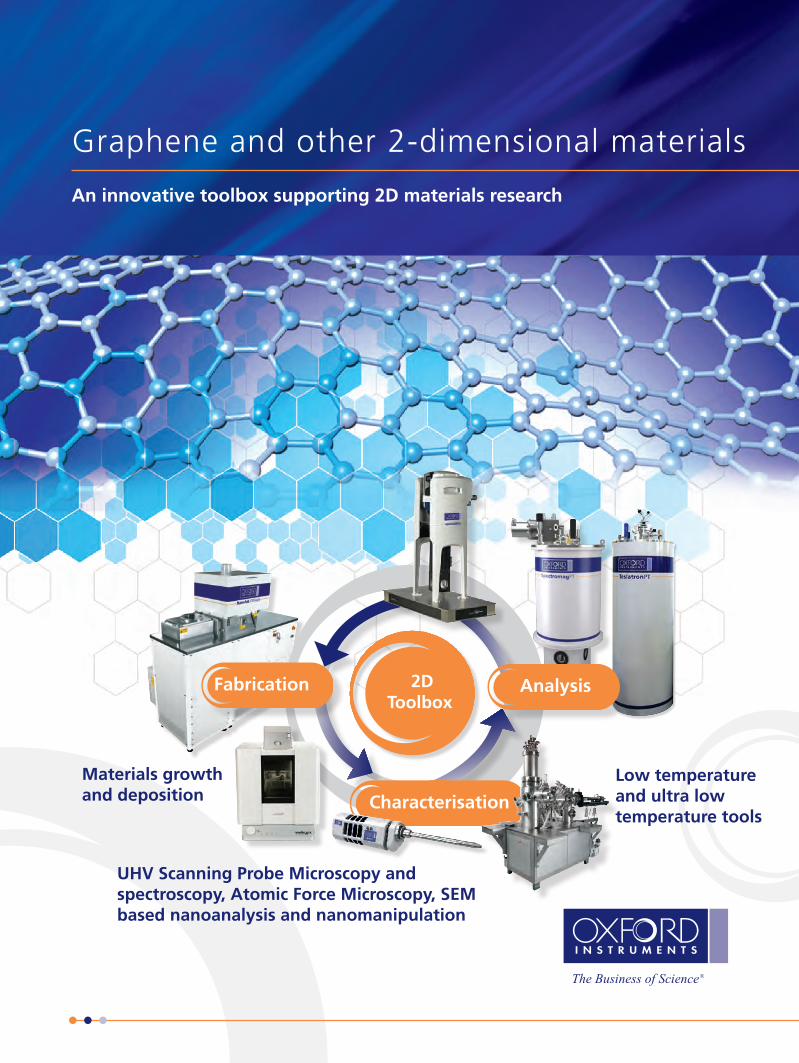
Atomic Layer Deposition (ALD)
High quality dielectric deposition on graphene
and 2D materials requires the use of ALD
The ALD product family encompasses a range of tools to meet the varied
demands of academia, corporate R&D and small scale production.
OpAL tool
• Open load thermal ALD tool with
plasma option
• Field upgrade available for plasma
option
• Small wafer pieces up to full
200mm wafers – equally suitable
for academic and industry R&D
FlexAL tool
• Remote plasma & thermal ALD
in one flexible tool
• Automated 200mm load lock for
process flexibility
• Clusterable for vacuum transfer of
substrates
• In situ ellipsometry options
ALD of many dielectric materials
possible through different co-reactants
allowing control of:
• Stoichiometry
• Aspect Ratio
• Temperature Range
Al2O3 HFO3 SiO2 Ta2O3 TiO3 ZrO2 SrTiO3
Water ✔ ✔ ✗ ✔ ✔ ✔ ✗
Ozone ✔ ✔ ✔
Plazma ✔ ✔ ✔ ✔ ✔ ✔ ✔
RoomTemp ✔ ✔ ✔
Study of nucleation delay1
The thickness of TiN films grown on different thermal SiO2 substrates
monitored by in-situ spectroscopic ellipsometry and shown as a function of
number of remote plasma ALD cycles. The inset displays the initial growth
region in more detail. Two substrates were prepared by the method of
calcination and preheated at temperatures of 750ºC and 1000ºC, the other
substrate was an as-received wafer with 410 nm thermal oxide.
1E. Langereis, S.B.S. Heil, M.C.M. van de Sanden, and W.M.M. Kessels, J.Appl. Phys. 100, 023534 (2006)
Plasma ALD of 80 nm Al2O
3 from TMA and
O2 plasma in a 10:1 aspect ratio deep trench
capacitor structure. Courtesy of Eindhoven University of Technology and NXP
Graphene 3
FABRICATE FABRICATE

Materials Deposition
Molecular Beam Epitaxy (MBE) allows deposition of novel materials with complex stoichiometry
resulting in exactly the desired material composition with precise control over atomic layer thickness.
Molecular Beam Epitaxy (MBE)
Molecular Beam Epitaxy (MBE) allows deposition of novel materials with complex stoichiometry resulting in exactly the desired
material composition with precise control over atomic layer thickness. The new MBE series of systems fulfil the most stringent
requirements of modern nanotechnology research moving from thin films towards individual 2 dimensional atomic layers.
Omicron MBE systems employ state-of-the-art components for the MBE growth which find applications in deposition of 2D
semiconductors and topological insulators.
Modular Systems LAB-10 & EVO-25/-50 & PRO-75/-100
• Sophisticated substrate manipulators for continuous
rotation at high temperature (up to 1400°C)
• Standard MBE sources with various crucible sizes (1.5 cm3
up to 200 cm3)
• Specifically designed MBE sources for elemental &
compound evaporation or sublimation in a temperature
range from less than 70°C to more than 2000°C (suitable
for low or high growth rates and extremely pure doping
conditions
• In-situ growth control (RHEED, ellipsometry, Quartz Micro
Balance, Beam Flux Monitor, RGA etc.)
• A wide range of Electron Beam Evaporators (EFM, EBVV
and EBV series) which are ideal for high-purity evaporation
in UHV, ranging from refractory metals (e.g. from rods,
wires or crucibles) to delicate reactive substances
• Seamless integration with an analysis module into a single
system
• The EPI-Soft process control software allows growth control
of the most sophisticated and complex layer structures
- with just a mouse click.
MBE growth of Bi2Te
3
topological insulator. (a) RHEED pattern and (b) STM image of 50QL Bi
2Te
3 (c) ARPES
spectra of the film.
Courtesy of Yi Zhang and Qi-Kun Xue et al Institute of Physics, Chinese Academy of Sciences, Beijing 100190, China.
Lab-10
4 Graphene
FABRICATE

Optical Characterisation
Molecular Beam Epitaxy (MBE) allows deposition of novel materials with complex stoichiometry
resulting in exactly the desired material composition with precise control over atomic layer thickness.
Optical Spectroscopy and Detection Solutions
Spectroscopic analysis of single or multi layer crystalline structures can provide a valuable insight
into number and orientation of layers, level of defects and quality and type of edges.
Gaining a greater and more complete understanding of these structures requires increasingly
complex detection setups where multiple characterization techniques can be combined.
Developing such novel and specialized systems often require researchers to consider a
modular configuration approach.
• High sensitivity detectors - comprehensive portfolio of CCD, EMCCD and InGaAs cameras
• Long lasting detection performance - UltraVac™ technology with advanced TE-cooling
down to -100ºC
• Modular spectrograph platforms - Seamlessly configurable, high throughput
Czerny-Turner, Echelle and Transmission designs
• Micro-spectroscopy interfaces - highly configurable cage system-based options
• Raman spectroscopy
• Luminescence / Photoluminescence
• Tip-Enhanced Raman Spectroscopy (TERS)
• Hyperspectral / chemical mapping
Modular micro-spectroscopy setup with single photon sensitive Newton EMCCD camera, Shamrock spectrograph and cage system coupling.
Graphene 5
FABRICATE CHARACTERISE

Scanning Probe Microscopy in UHV
6 Graphene
For Graphene research, Omicron Nanoscience offers a wide variety of SPM
techniques for UHV at variable temperatures (from 15 K to 1500 K), low temperature
applications (down to 0.5 K) or for large samples of up to 4“ in diameter. These
instruments are available both as system solutions or as stand-alone components.
Omicron LT-STM
Atomic resolution STM image of a graphene flake on a SiO2 substrate.
Y. Zhang, M. Cromie, Lawrence Berkeley Laboratory,USA (Nature Physics 4, 2008) A
An Omicron LT STM and VT STM are used to image the Graphene Nano Ribbons( GNR). The STM image shows a threefold junction of a GNR. Data courtesy of R. Fasel, Empa, Swiss Federal Laboratories for Materials Science and Technology, Duebendorf, Switzerland. Literature: Nature 466, 470-473 (2010)
Investigation of defects in graphene using an Omicron Q-plus SPM. Joost van der Lit et al, Nature Comms. 2013
STM & AFM
CHARACTERISE

Electron Spectroscopy and Nanoprobing
We have developed sophisticated instrumental concepts, to enable the combination of a broad
range of analysis and nano-structuring techniques. Our product range for Graphene includes:
• Scanning Electron/Auger Microscopy (SEM/SAM)
• Photo Electron Spectroscopy (XPS, UPS) Chemical
analysis (XPS core levels, UPS valence levels)
• Angle-resolved Photo Electron Spectroscopy
(ARPES, ARUPS, ARXPS) k-space bandstructures
• Photo Emission Electron Microscopy
(NanoESCA, K-PEEM)
• 3D k-space maps of bandstructures The NanoESCA is a sophisticated surface characterization instrument designed for highest resolution imaging XPS, angle resolved UPS and PEEM. It offers 10 times better imaging XPS resolution than presently commercially available instrumentation.
3D plot of the band structure of Graphene (0-15 eV binding energy). N. Barrett, E. Conrad (IRAMIS, GeorgiaTech)
Nanoprobing - Local electrical characterisation on the nanoscale
LT NanoProbe. T<4K. Atomic resolution STM with 4 probes. SEM navigated*
Direction dependant transport characteristics in graphene. Anisotropic conductivity observed due to charge buildup at step edges in epitaxial graphene leads to local scattering of charge carriers*
*Naval Research Laboratory,Washington, D.C., USA (Nano Lett 2010, 10)
Graphene 7
CHARACTERISE CHARACTERISE

Ambient AFM
8 Graphene
It is notoriously difficult to quickly characterise 2D materials mounted on a substrate.
Oxford Instruments provides a suite of leading edge atomic force microscopes with a
wide range of working modes and options that can do the task in minutes.
AFM of graphene on copper1
CHARACTERISECharacterising topography and electromechanical properties
Determining the orientation of the graphene lattice: (a) Lattice resolution lateral deflection image of graphene on copper, (b) FFT of the AFM image with a hexagon overlaid indicating the expected atomic lattice structure.1
Go beyond topography
with Asylum Research AFMs
• High resolution topography – from single atomic point
defects up to 90 μm scans
• Nanomechanical properties – storage and loss moduli
• Thermal properties – temperature and thermal transitions
• Electrical properties – current, resistance / conductivity,
capacitance / permittivity
• Properties under controlled gas and liquid environments
sDNA and dsDNA mixture adsorbed on graphene, 1.7 μm scan. Imaged with the CypherTM S AFM.2
Scanning Microwave Microscopy distinguishes regions with two or three graphene layers based on their higher conductivity.3
1 Courtesy of A.J. Marsden and N.R. Wilson, University of Warwick. 2 Courtesy of Prof. Andras Kis, EPFL, Lausanne, Switzerland (Langmuir 2010, 26(23): 18078). 3 Courtesy of Alexander Tselev, Oak Ridge National Laboratory (Nanotechnology 2012, 23(38):385706).

Electron beam diffraction and X Ray analysis
Graphene 9
Characterise the number of 2D layers, contaminant and doping materials, the interface system,
the orientation of substrate grains at the nanoscale.
CHARACTERISE
• EDS and EBSD microanalysis systems fully
characterise 2D systems in the SEM - elements,
phases, substrate grain size and orientation
• LayerProbe® is a non-destructive EDS-
based solution for the fast and very accurate
mapping of the thickness of 2D
materials (see example below)
• Other tools for the SEM/FIB include
nanomanipulators and gas injection systems
Oxford Instruments’ LayerProbe confirms the elemental composition of an MoS
2 flake and
measures the thicknesses at two locations, clearly showing the presence of one layer versus two.
AFM image of the same flake using an Asylum Research Cypher AFM. Upper line profile indicates that there is one layer above the substrate, lower line profile indicates that a second layer is present. There is close correlation with the LayerProbe results on the left.
Characterising composition and structure in the SEM
The significance of characterising grain orientation by EBSD during graphene growth on polycrystalline copper foils is discussed by Niclas S. Müller et al., to be published in Carbon. Image courtesy of D. Abou-Ras, Helmholtz-Zentrum Berlin.
Analysis of a direct band gap 2D semiconductor
Molybdenum disulfide (MoS2) is a layered 2D material similar to
graphene. However, unlike Graphene it has a band gap which makes
it attractive for electronics and optoelectronics. Like Graphene, its
unique properties are strongly dependent on the number of layers -
these can be measured using Oxford Instruments equipment.
CHARACTERISE

Materials analysis and physical properties
Many phenomena can be studied at low or ultra-low temperature and high magnetic field
through different experimental techniques, in order to gain understanding of the fundamental
properties of graphene, nanotubes, nanowires, topological insulators and other 1D/2D materials.
This may be at a fundamental physics level, or to investigate the behaviour and control of
devices such as qubits.
Low and ultra-low temperature tools with integrated high magnetic fields
Our tools enable the study of such effects by providing these low temperature
and magnetic field sample environments, with an interface to signal paths and
characterising probes ranging from simple dc transport measurements to complex
optical or THz spectroscopy.
Integrated low temperature and high magnetic
field systems
Band structure, low temperature charge and spin carrier transport measurements
through effects such as Integral and Fractional Quantum Hall Effect (IQHE and
FQHE), superconducting proximity, Coulomb drag in graphene multilayers, etc.
The award-winning TritonTM Cryofree
dilution refrigerator
• Achieves less than 10 mK, with integrated magnet options up to
18 T providing the highest possible B/T ratios in Cryofree systems,
with fast sample cooldown and exchange options.
• Vector rotate magnets allow precise non-mechanical alignment of
field vector relative to low-dimensional samples for investigation or
utilisation of anisotropic properties in low dimensional materials
Cryofree integrated magnet systems
• Offer up to 18 Tesla (pictured) with an integral 1.5 K variable
temperature insert, with additional milliKelvin insert options
• Range of magnetic field, sample space and
sample probe options for maximum flexibility
• Liquid helium cooled magnet systems extend up to a
state-ofthe-art 22 Tesla
Integer Quantum Hall Effect measurementobtained with a 14 T superconducting magnetand HelioxVL 3He insert. Courtesy of Dr KostyaNovoselov, University of Manchester, UK.
TritonTM Cryofree dilution refrigerator
10 Graphene
ANALYSE

Materials analysis and physical properties
Graphene 11
Optical low temperature and high magnetic field systemsModerate to long working-distance cryostats enable low temperature optical spectroscopy
demonstrated in measurement techniques such as magneto-optical effects, free space
microwave spectroscopy, THz transmittance spectroscopy, etc.
Low and ultra-low temperature tools with integrated high magnetic fields
New OptistatDry
3 K Cryofree cryostat
Can be optimised for a wide range of
spectroscopy techniques, giving optical
excellence through a wide range of window
materials, and flexibility with a large clear
view, an f1 angle, and easy in-the-lab
replaceable windows
Spectromag®PT Cryofree
magneto-optical systems
Combine a 7 T magnetic field
with integrated 1.5 K variable
temperature insert
The renowned, compact MicrostatHe
short working distance cryostat
Enables low temperature confocal spectro-microscopy down
to 4 K with techniques including Raman, optical absorption,
FTIR, and time-resolved spectroscopy such as pump-probe
measurements and photocurrent microscopy. Its class-leading
helium consumption ensures the lowest possible low running
costs, and is frequently combined on optical benches with an
Oxford Instruments Andor spectroscopy detector.
ANALYSE ANALYSE

visit www.oxford-instruments.com for more information
Oxford Instruments, at Yatton, UK, operates Quality Management Systems approved to the requirements of BS EN ISO 9001. This publication is the copyright of Oxford Instruments plc and provides outline information only, which (unless agreed by the company in writing) may not be used, applied or reproduced for any purpose or form part of any order or contract or regarded as the representation relating to the products or services concerned. Oxford Instruments’ policy is one of continued improvement. The company reserves the right to alter without notice the specification, design or conditions of supply of any product or service. Oxford Instruments acknowledges all trademarks and registrations. © Oxford Instruments plc, 2014. All rights reserved. Ref: OI/Graphene/2014/01
Oxford Instruments
www.oxford-instruments.com
Global service, support, training, consumables and accessories
2778
We employ skills, knowledge and enthusiasm to deliver a world-class service that exceeds your expectations.Oxford Instruments is committed to supporting our customers’ success. We recognise that
this requires world class products complimented by world class support.
Email: [email protected]
www.oxford-instruments.com/2D


![THREE-DIMENSIONAL GRAPHENE-BASED HYDROGEL/AEROGEL · PDF fileThree-dimensional graphene-based hydrogel/aerogel materials 137 o( 4SeP]RTSFcdSh6T]cTa6A "cS Rev. Adv. Mater. Sci. 36 (2014)](https://img.dokumen.tips/doc/110x75/5a8c54b07f8b9af27f8c44a4/three-dimensional-graphene-based-hydrogelaerogel-graphene-based-hydrogelaerogel.jpg)