Embed Size (px)
Citation preview

GPU
JUNE 6TH2019

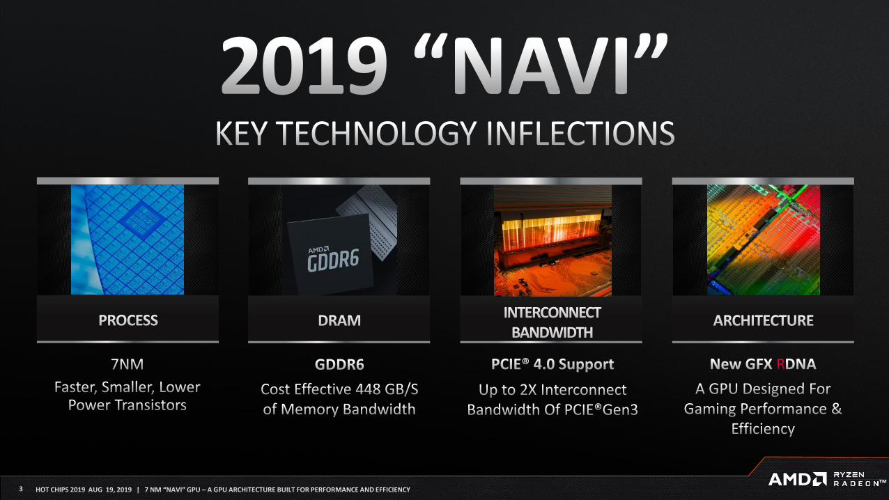
7nm
251 sqmm
10.3 Billion Transistors
X16 PCIe® Gen 4.0
8 GB GDDR6 256b @14 Gbps
448 GB/S*
2560 Stream Processors
Up To 9.75 TFLOPs
*256 pin G6 * 14 Gbps *1B/8b = 448 GBS
®
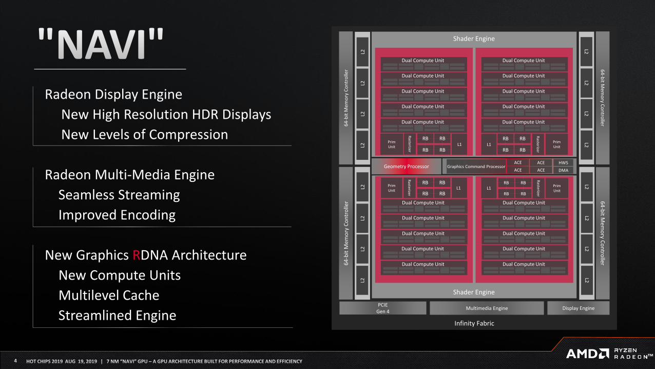
Radeon Display Engine
New High Resolution HDR Displays
New Levels of Compression
Radeon Multi-Media Engine
Seamless Streaming
Improved Encoding
New Graphics RDNA Architecture
New Compute Units
Multilevel Cache
Streamlined EngineInfinity Fabric
PCIE
Gen 4Display EngineMultimedia Engine
Geometry Processor
Shader Engine
Graphics Command ProcessorACE ACE
ACE ACE
HWS
DMA
64
-bit
Me
mo
ry C
on
tro
lle
r6
4-b
it M
em
ory
Co
ntr
olle
r 64
-bit M
em
ory
Co
ntro
ller
64
-bit M
em
ory
Co
ntro
ller
Dual Compute Unit
Dual Compute Unit
Dual Compute Unit
Dual Compute Unit
Dual Compute Unit
L1Prim
UnitL1
Prim
Unit
Dual Compute Unit
Dual Compute Unit
Dual Compute Unit
Dual Compute Unit
Dual Compute Unit
Dual Compute Unit
Dual Compute Unit
Dual Compute Unit
Dual Compute Unit
Dual Compute Unit
L1Prim
UnitL1
Prim
Unit
Dual Compute Unit
Dual Compute Unit
Dual Compute Unit
Dual Compute Unit
Dual Compute Unit
Ra
sterize
r
Ra
sterize
rR
aste
rizer
Ra
sterize
r
Shader Engine
RB
RB
RB
RB
RB
RB
RB
RB
RB
RB
RB
RB
RB
RB
RB
RB
L2L2
L2L2
L2L2
L2L2
L2L2
L2L2
L2L2
L2L2
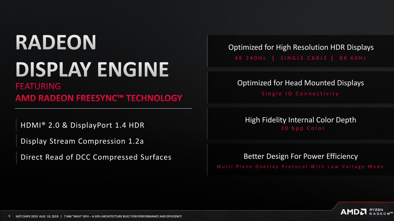
High Fidelity Internal Color Depth3 0 b p p C o l o r
Optimized for High Resolution HDR Displays
4 K 2 4 0 H z | S I N G L E C A B L E | 8 K 6 0 H z
Optimized for Head Mounted Displays
S i n g l e I O C o n n e c t i v i t y
Better Design For Power Efficiency
M u l t i P l a n e O v e r l a y P r o t o c o l W i t h L o w V o l t a g e M o d e
HDMI® 2.0 & DisplayPort 1.4 HDR
Display Stream Compression 1.2a
Direct Read of DCC Compressed Surfaces
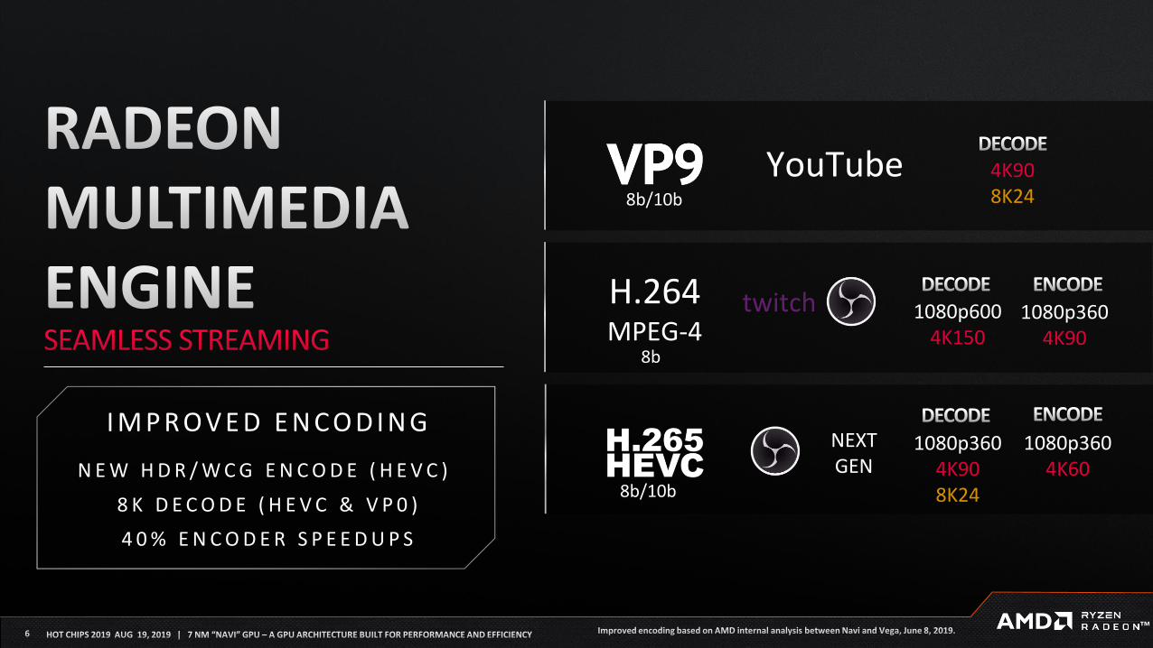
H.264MPEG-4
1080p600
4K150
1080p360
4K90
1080p360
4K60
1080p360
4K90
8K24
NEXT
GEN
4K90
8K24
I M P R OV E D E N C O D I N G
N E W H D R / W C G E N C O D E ( H E V C )
8 K D E C O D E ( H E V C & V P 0 )
4 0 % E N C O D E R S P E E D U P S
YouTube
twitch
8b/10b
8b
8b/10b

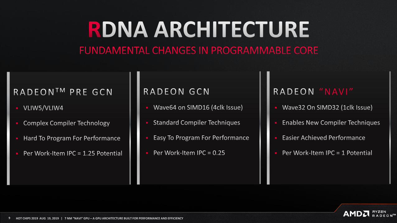
Motivation
Radeon Architecture
New Compute Unit
Multi-Level Cache
Streamlined Engine
Results & Example
GPU Architecture Designed For
Gaming Performance & Efficiency

T H E M OT I VAT I O N B E H I N D N AV I A R C H I T E C T U R E
▪
▪
▪
▪
▪
▪
▪
▪
“ N AV I ”▪
▪
▪
▪

2X INSTRUCTION RATE
Dual Schedulers
Dual Scalar Units
Dual SIMD32
SINGLE CYCLE ISSUE
Wave32 on SIMD32
ALU & LD/ST Unit
SFU Co-Execution
BYTES PER FLOP
128B Load/Store
64B Filter Rate
EXECUTION FLEXIBILITY
Wave64 Dual Issue
Cooperating CU Pair

LDS RTN
IDX DIRECT
VECTOR
MEM RTN
V INIT
DATA

▸
▸
▸
▸
▸
▸
▸
▸
▸
▸
▸
▸
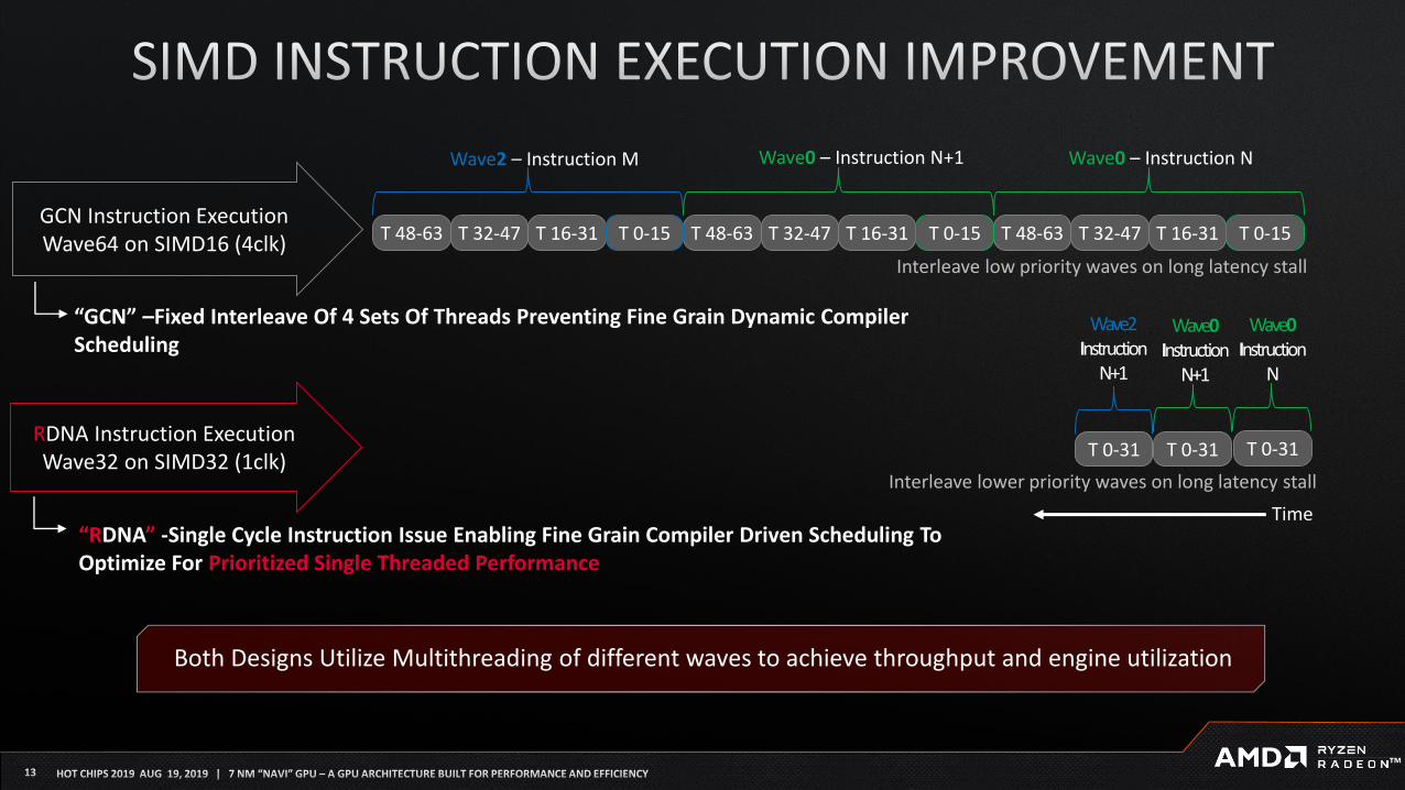
Interleave low priority waves on long latency stall
Wave2 – Instruction M Wave0 – Instruction N+1 Wave0 – Instruction N
T 32-47 T 16-31 T 0-15T 48-63T 32-47 T 16-31 T 0-15T 48-63T 32-47 T 16-31 T 0-15T 48-63GCN Instruction Execution
Wave64 on SIMD16 (4clk)
“GCN” –Fixed Interleave Of 4 Sets Of Threads Preventing Fine Grain Dynamic Compiler
SchedulingWave0
Instruction
N
T 0-31RDNA Instruction Execution
Wave32 on SIMD32 (1clk)
“RDNA” -Single Cycle Instruction Issue Enabling Fine Grain Compiler Driven Scheduling To
Optimize For Prioritized Single Threaded Performance
T 0-31T 0-31
Wave0
Instruction
N+1
Wave2
Instruction
N+1
Time
Interleave lower priority waves on long latency stall
Both Designs Utilize Multithreading of different waves to achieve throughput and engine utilization

RDNA
2 Wave 32 ➔ 2 SIMD32
Instruction Issue ➔ 1 clock
CU ALU ➔ 100% Utilized
ILP unlocks up to 4x faster focused execution
Engage Machine Quickly By Uniformly Distributing Work To All ALUs
Optimize Efficiency And Latency By Preferring Highest Priority/Oldest Work
Extract Program ILP And Scheduling To Benefit From Data Locality
Utilize Multi-Threading Of Waves To Hide Remaining Latencies For Throughput
WORK LOAD EXAMPLE: 64 WORK-ITEMS ALU INTENSIVE CODE
0 31 0 31
SIMD 0 SIMD 1S
GCN
1 Wave64 ➔ SIMD16
Instruction Issue ➔ 4 clock
CU ALU ➔ 25% Utilized
Effective Throughput
0 15
SIMD 00 15
SIMD 10 15
SIMD 20 15
SIMD 3S
R

▪
▪
▪
▪
▪
▪
▪
▪
▸
▸
▸
SIMD32
Wave32
SIMD32
Wave64

0
1
2
3
4
5
6
7
8
9
10
11
12
13
14
15
s_add_i32 s0, s1, s2
…
…
…
v_mul_f32 v0, v1, s0
… (simd busy 4 cycles)
…
…
v_add_f32 v5, v4, v3
…
…
…
v_sub_f32 v6, v7, v0
…
…
…
s_add_i32 s0, s1, s2
v_mul_f32 v0, v1, s0
v_add_f32 v5, v4, v3
v_sub_f32 v6, v7, v0
s_add_i32 s0, s1, s2
… (salu dependency stall on S0)
v_mul_f32 v0, v1, s0
v_add_f32 v5, v4, v3
… (valu dependency stall on V0)
…
…
v_sub_f32 v6, v7, v0
s_add_i32 s0, s1, s2
… (salu dependency stall on S0)
v_mul_f32 v0, v1, s0 (lo)
v_mul_f32 v0, v1, s0 (hi)
v_add_f32 v5, v4, v3 (lo)
v_add_f32 v5, v4, v3 (hi)
… (valu dependency stall on V0 lo)
v_sub_f32 v6, v7, v0 (lo)
v_sub_f32 v6, v7, v0 (hi)
SHORTEST
WAVE ISSUE
LATENCY
44%
REDUCTION IN
ISSUE CYCLES

▪
▪
▪
▪
▸
▸

ACCESS TO
2XRegisters
UP TO
2XALUs
Compute Unit 1
Compute Unit 0
ACCESS TO
4XCache Bandwidth

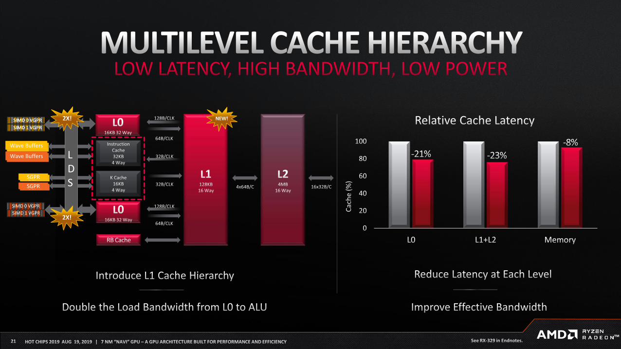
New L1 Level Cache
Improved Bandwidth Amplification
Reduced Latency and Power
Reduced Congestion at L2 Level
Infinity Fabric
PCIE
Gen 4Display EngineMultimedia Engine
Geometry Processor
Shader Engine
Graphics Command
Processor
ACE ACE
ACE ACE
HWS
DMA
64
-bit
Me
mo
ry C
on
tro
lle
r6
4-b
it M
em
ory
Co
ntr
olle
r 64
-bit M
em
ory
Co
ntro
ller
64
-bit M
em
ory
Co
ntro
ller
Dual Compute Unit
Dual Compute Unit
Dual Compute Unit
Dual Compute Unit
Dual Compute Unit
L1Prim
UnitL1
Prim
Unit
Dual Compute Unit
Dual Compute Unit
Dual Compute Unit
Dual Compute Unit
Dual Compute Unit
Dual Compute Unit
Dual Compute Unit
Dual Compute Unit
Dual Compute Unit
Dual Compute Unit
L1Prim
UnitL1
Prim
Unit
Dual Compute Unit
Dual Compute Unit
Dual Compute Unit
Dual Compute Unit
Dual Compute Unit
Ra
sterize
r
Ra
sterize
rR
aste
rizer
Ra
sterize
r
Shader Engine
RB
RB
RB
RB
RB
RB
RB
RB
RB
RB
RB
RB
RB
RB
RB
RB
L2L2
L2L2
L2L2
L2L2
L2L2
L2L2
L2L2
L2L2
L0
L0
L0
L0
L0
L0
L0
L0
L0
L0
L0
L0
L0 L0
L0
L0
L0
L0
L0
L0

Unified LLC for GFX/ACE Pipes
Instruction Range Based Actions
OOO between R/W, L0, L1, L2, Mem
Reduced Latency and Power
Reduced Data Movement
WGP
WGP
WGP
WGP
WGP
WGP
WGP
WGP
WGP
WGP
WGP
WGP
WGP
WGP
WGP
WGP
WGP
WGP
WGP
WGP
SGPR
SGPR
Wave Buffers
Wave Buffers
SGPR
SIMD 1 VGPR
SIMD 1 VGPR
SGPR
Wave Buffers
Wave Buffers
L
D
S
SIMD 0 VGPR
SIMD 0 VGPR

Shader
ComplexPCIe® 4.0 Geometry
Async Compute
Command
Interfaces
Compressed Data
SOC Fabric
Rasterizer &
L1
Texture
DISPLAY
ENGINE


0%
20%
40%
60%
80%
100%
See Endnotes "RX-325 and RX-362. Data based on AMD internal testing 6/1/2019.

See Endnotes RX-325, RX-358, and RX-365.
Slide data based on AMD internal testing 6/1/2019.
14 nm “Vega64” 7nm “Navi”

▸
▸
▸
▸
R
▸
▸
Vector Instruction IssueWaveId
One SIMD Instruction trace of oldest wave (12), next to oldest wave (13), etc
Waiting to be executedStore ResultsSFU Instruction
Scalar Mem Instruction

™