Embed Size (px)
DESCRIPTION
GPIB ASIC uPD7210 compatible
Citation preview

© Copyright 1994, 1995 National Instruments Corporation.All Rights Reserved.
NAT7210TM
Reference Manual
June 1995 Edition
Part Number 370875A-01

National Instruments Corporate Headquarters6504 Bridge Point ParkwayAustin, TX 78730-5039(512) 794-0100Technical support fax: (800) 328-2203
(512) 794-5678
Branch Offices:Australia 03 9 879 9422, Austria 0662 45 79 90 0, Belgium 02 757 00 20,Canada (Ontario) 519 622 9310, Canada (Québec) 514 694 8521,Denmark 45 76 26 00, Finland 90 527 2321, France 1 48 14 24 24,Germany 089 741 31 30, Hong Kong 2645 3186, Italy 02 48301892,Japan 03 5472 2970, Korea 02 596 7456, Mexico 5 202 2544,Netherlands 03480 33466, Norway 32 84 84 00, Singapore 2265886,Spain 91 640 0085, Sweden 08 730 49 70, Switzerland 056 20 51 51,Taiwan 02 377 1200, U.K. 01635 523545

Limited Warranty
The NAT7210™ integrated circuit (“equipment”) is warranted against defects in materialand workmanship under normal use and service for a period of one (1) year from the dateof shipment from the National Instruments factory. During this period of one year,National Instruments shall at its sole option either repair, replace, or credit the Buyer fordefective equipment if: (i) Buyer returns the equipment to National Instruments, FOB theNational Instruments factory in Austin, Texas; (ii) Buyer notifies National Instrumentspromptly upon discovery of any defect in writing, including a detailed description of thedefect; and (iii) upon examination of the returned equipment, National Instruments issatisfied that the circuit is defective and that the cause of such defect is not alteration orrepair by someone other than National Instruments, neglect, accident, misuse, improperinstallation, or use contrary to any instructions issued by National Instruments.
A Return Material Authorization (RMA) number must be obtained from the factory andclearly marked on the outside of the package before any equipment will be accepted forwarranty work. Prior to issuance of an RMA by National Instruments, Buyer shall allowNational Instruments the opportunity to inspect the equipment on-site at Buyer’s facility.
This warranty expires one year from date of original shipment regardless of any warrantyperformance during that warranty period. The warranty provided herein is Buyer’s soleand exclusive remedy for nonconformity of the equipment or for breach of any warranty.THE ABOVE IS IN LIEU OF ALL OTHER WARRANTIES EXPRESSED ORIMPLIED. NATIONAL INSTRUMENTS SPECIFICALLY DISCLAIMS THEIMPLIED WARRANTIES OF MERCHANTIBILITY AND FITNESS FOR APARTICULAR PURPOSE. BUYER’S RIGHT TO RECOVER DAMAGES CAUSEDBY FAULT OR NEGLIGENCE ON THE PART OF NATIONAL INSTRUMENTSSHALL BE LIMITED TO THE AMOUNT THERETOFORE PAID BY THE BUYER.NATIONAL INSTRUMENTS WILL NOT BE LIABLE FOR DAMAGES RESULTINGFROM LOSS OF DATA, PROFITS, USE OF PRODUCTS, OR INCIDENTAL ORCONSEQUENTIAL DAMAGES, EVEN IF ADVISED OF THE POSSIBILITYTHEREOF. This limitation of the liability of National Instruments will apply regardlessof the form of action, whether in contract or tort, including negligence. NationalInstruments recommends against the use of its products as critical components in any lifesupport devices or systems whose failure to perform can reasonably be expected to causesignificant injury to a human. Buyer assumes all risk for such application and agrees toindemnify National Instruments for all damages which may be incurred due to use of theNational Instruments standard devices in medical or life support applications. Any actionagainst National Instruments must be brought within one year after the cause of actionaccrues.
National Instruments believes that the information in this manual is accurate. Thedocument has been carefully reviewed for technical accuracy. In the event that technicalor typographical errors exist, National Instruments reserves the right to make changes tosubsequent editions of this document without prior notice to holders of this edition. Thereader should consult National Instruments if errors are suspected. In no event shallNational Instruments be liable for any damages arising out of or related to this documentor the information contained in it.

Copyright
Under the copyright laws, this publication may not be reproduced or transmitted in anyform, electronic or mechanical, including photocopying, recording, storing in aninformation retrieval system, or translating, in whole or in part, without the prior writtenconsent of National Instruments Corporation.
Trademarks
NAT7210™ is a trademark of National Instruments Corporation.
Product and company names listed are trademarks or trade names of their respectivecompanies.
WARNING REGARDING MEDICAL AND CLINICALUSE OF NATIONAL INSTRUMENTS PRODUCTS
National Instruments products are not designed with components and testing intended toensure a level of reliability suitable for use in treatment and diagnosis of humans.Applications of National Instruments products involving medical or clinical treatment cancreate a potential for accidental injury caused by product failure, or by errors on the partof the user or application designer. Any use or application of National Instrumentsproducts for or involving medical or clinical treatment must be performed by properlytrained and qualified medical personnel, and all traditional medical safeguards,equipment, and procedures that are appropriate in the particular situation to preventserious injury or death should always continue to be used when National Instrumentsproducts are being used. National Instruments products are NOT intended to be asubstitute for any form of established process, procedure, or equipment used to monitoror safeguard human health and safety in medical or clinical treatment.
© National Instruments Corp. v NAT7210 Reference Manual
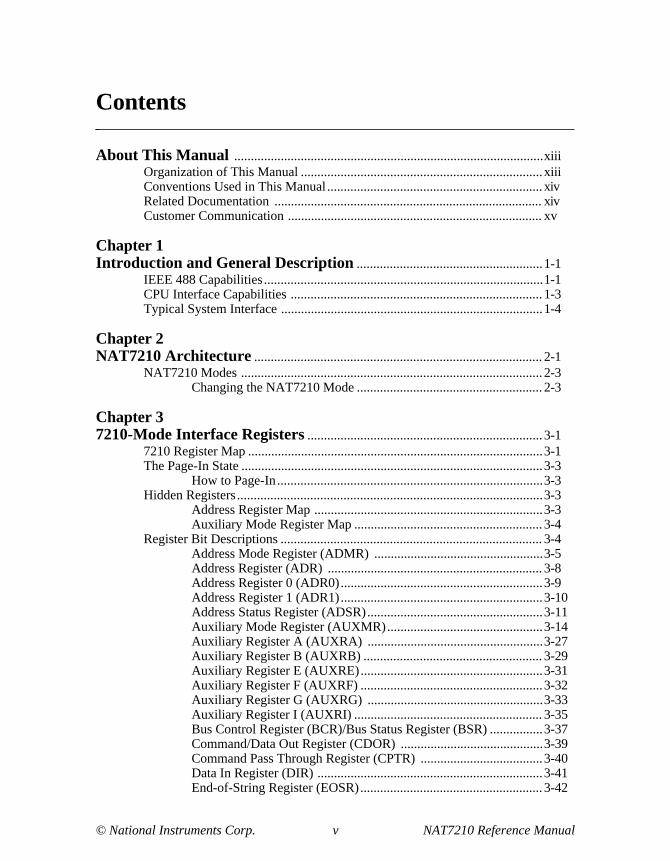
Contents
About This Manual ............................................................................................. xiiiOrganization of This Manual ......................................................................... xiiiConventions Used in This Manual ................................................................. xivRelated Documentation ................................................................................. xivCustomer Communication ............................................................................. xv
Chapter 1Introduction and General Description ........................................................ 1-1
IEEE 488 Capabilities .................................................................................... 1-1CPU Interface Capabilities ............................................................................ 1-3Typical System Interface ............................................................................... 1-4
Chapter 2NAT7210 Architecture ....................................................................................... 2-1
NAT7210 Modes ........................................................................................... 2-3Changing the NAT7210 Mode ........................................................ 2-3
Chapter 37210-Mode Interface Registers ....................................................................... 3-1
7210 Register Map ......................................................................................... 3-1The Page-In State ........................................................................................... 3-3
How to Page-In................................................................................ 3-3Hidden Registers ............................................................................................ 3-3
Address Register Map ..................................................................... 3-3Auxiliary Mode Register Map ......................................................... 3-4
Register Bit Descriptions ............................................................................... 3-4Address Mode Register (ADMR) ................................................... 3-5Address Register (ADR) ................................................................. 3-8Address Register 0 (ADR0)............................................................. 3-9Address Register 1 (ADR1)............................................................. 3-10Address Status Register (ADSR)..................................................... 3-11Auxiliary Mode Register (AUXMR)............................................... 3-14Auxiliary Register A (AUXRA) ..................................................... 3-27Auxiliary Register B (AUXRB) ...................................................... 3-29Auxiliary Register E (AUXRE)....................................................... 3-31Auxiliary Register F (AUXRF) ....................................................... 3-32Auxiliary Register G (AUXRG) ..................................................... 3-33Auxiliary Register I (AUXRI) ......................................................... 3-35Bus Control Register (BCR)/Bus Status Register (BSR) ................ 3-37Command/Data Out Register (CDOR) ........................................... 3-39Command Pass Through Register (CPTR) ..................................... 3-40Data In Register (DIR) .................................................................... 3-41End-of-String Register (EOSR)....................................................... 3-42

Contents
NAT7210 Reference Manual vi © National Instruments Corp.
Internal Count Register (ICR) ......................................................... 3-43Internal Count Register 2 (ICR2) .................................................... 3-44Interrupt Mask Register 0 (IMR0)................................................... 3-45Interrupt Status Register 0 (ISR0) ................................................... 3-45Interrupt Mask Register 1 (IMR1)................................................... 3-49Interrupt Status Register 1 (ISR1) ................................................... 3-49Interrupt Mask Register 2 (IMR2)................................................... 3-54Interrupt Status Register 2 (ISR2) ................................................... 3-54Parallel Poll Register (PPR) ............................................................ 3-58Source/Acceptor Status Register (SASR) ....................................... 3-60Serial Poll Mode Register (SPMR) ................................................. 3-62Serial Poll Status Register (SPSR) .................................................. 3-62Version Status Register (VSR)........................................................ 3-64
Chapter 49914-Mode Interface Registers ....................................................................... 4-1
9914 Register Map ......................................................................................... 4-1The Page-In Condition ................................................................................... 4-3Hidden Registers ............................................................................................ 4-3
Accessory Read Register Map......................................................... 4-3Register Bit Descriptions ............................................................................... 4-4
Accessory Register A (ACCRA) ..................................................... 4-5Accessory Register B (ACCRB) ..................................................... 4-6Accessory Register E (ACCRE) ..................................................... 4-8Accessory Register F (ACCRF) ...................................................... 4-9Accessory Register I (ACCRI)........................................................ 4-10Address Register (ADR) ................................................................. 4-11Address Status Register (ADSR)..................................................... 4-12Auxiliary Command Register (AUXCR) ........................................ 4-15Bus Control Register (BCR)/Bus Status Register (BSR) ................ 4-28Command/Data Out Register (CDOR) ........................................... 4-30Command Pass Through Register (CPTR) ..................................... 4-31Data In Register (DIR) .................................................................... 4-32End-of-String Register (EOSR)....................................................... 4-33Internal Count Register (ICR) ......................................................... 4-34Interrupt Mask Register 0 (IMR0)................................................... 4-35Interrupt Status Register 0 (ISR0) ................................................... 4-35Interrupt Mask Register 1 (IMR1)................................................... 4-39Interrupt Status Register 1 (ISR1) ................................................... 4-39Interrupt Mask Register 2 (IMR2)................................................... 4-44Interrupt Status Register 2 (ISR2) ................................................... 4-44Parallel Poll Register (PPR) ............................................................ 4-48Serial Poll Mode Register (SPMR) ................................................. 4-49Serial Poll Status Register (SPSR) .................................................. 4-49

Contents
© National Instruments Corp. vii NAT7210 Reference Manual
Chapter 5Software Considerations ................................................................................... 5-1
Chip Initialization Sequence .......................................................................... 5-11. Place the NAT7210 in 7210 Mode ............................................. 5-12. Make Sure the Local pon Message Is Asserted.......................... 5-13. Set the Clock Frequency............................................................. 5-14. Configure the Chip for GPIB Operation .................................... 5-2
A. Set the GPIB Address(es) .......................................... 5-2B. Write the Initial Serial Poll Response........................ 5-2C. Configure Initial Parallel Response ........................... 5-2D. Set GPIB Handshake Parameters ............................... 5-2
5. Enable Interrupts ........................................................................ 5-26. Clear the Local pon Message ..................................................... 5-3
GPIB Talker or Listener Considerations ....................................................... 5-3GPIB Addressing ............................................................................. 5-3
Logical and Physical Devices ........................................... 5-3Normal and Extended Addressing .................................... 5-3Implementing One Logical Device: NormalAddressing ........................................................................ 5-3Implementing One Logical Device: ExtendedAddressing ........................................................................ 5-4Implementing Two Logical Devices: NormalAddressing ........................................................................ 5-4Implementing Two Logical Devices: ExtendedAddressing ........................................................................ 5-5Implementing Three or More Logical Devices:Normal Addressing ........................................................... 5-5Implementing Three or More Logical Devices:Extended Addressing ........................................................ 5-6
Programmed Implementation of a Talker and Listener................... 5-7Detecting a GPIB Listener ............................................................... 5-7
Sending GPIB Data Messages ....................................................................... 5-7Basic Flow ....................................................................................... 5-7Sending EOI or EOS ....................................................................... 5-8Using DMA ..................................................................................... 5-8T1 Delay Generation ....................................................................... 5-8
The T1 Delay .................................................................... 5-8HSTS Definition ............................................................... 5-9IEEE 488.1 Standard Requirements ................................. 5-9T1 Delay: 7210 Mode ...................................................... 5-10T1 Delay: 9914 Mode ...................................................... 5-10Using nbaf ......................................................................... 5-11
Receiving GPIB Data Messages .................................................................... 5-11Basic Flow ....................................................................................... 5-11Receiving END or EOS ................................................................... 5-11Performing an RFD Holdoff on the Last Data Byte........................ 5-12Using DMA ..................................................................................... 5-12
Acceptor Handshake Holdoffs ....................................................................... 5-12
Contents
NAT7210 Reference Manual viii © National Instruments Corp.
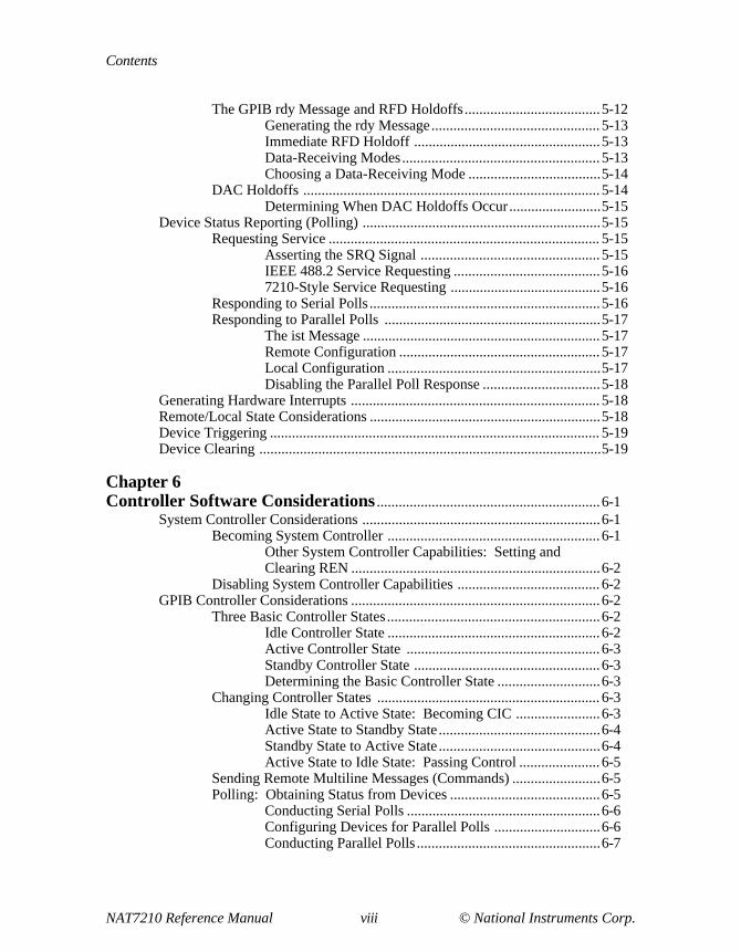
The GPIB rdy Message and RFD Holdoffs ..................................... 5-12Generating the rdy Message.............................................. 5-13Immediate RFD Holdoff ................................................... 5-13Data-Receiving Modes...................................................... 5-13Choosing a Data-Receiving Mode .................................... 5-14
DAC Holdoffs ................................................................................. 5-14Determining When DAC Holdoffs Occur......................... 5-15
Device Status Reporting (Polling) ................................................................. 5-15Requesting Service .......................................................................... 5-15
Asserting the SRQ Signal ................................................. 5-15IEEE 488.2 Service Requesting ........................................ 5-167210-Style Service Requesting ......................................... 5-16
Responding to Serial Polls ............................................................... 5-16Responding to Parallel Polls ........................................................... 5-17
The ist Message ................................................................. 5-17Remote Configuration ....................................................... 5-17Local Configuration .......................................................... 5-17Disabling the Parallel Poll Response ................................ 5-18
Generating Hardware Interrupts .................................................................... 5-18Remote/Local State Considerations ............................................................... 5-18Device Triggering .......................................................................................... 5-19Device Clearing ............................................................................................. 5-19
Chapter 6Controller Software Considerations ............................................................. 6-1
System Controller Considerations ................................................................. 6-1Becoming System Controller .......................................................... 6-1
Other System Controller Capabilities: Setting andClearing REN .................................................................... 6-2
Disabling System Controller Capabilities ....................................... 6-2GPIB Controller Considerations .................................................................... 6-2
Three Basic Controller States.......................................................... 6-2Idle Controller State .......................................................... 6-2Active Controller State ..................................................... 6-3Standby Controller State ................................................... 6-3Determining the Basic Controller State ............................ 6-3
Changing Controller States ............................................................. 6-3Idle State to Active State: Becoming CIC ....................... 6-3Active State to Standby State ............................................ 6-4Standby State to Active State ............................................ 6-4Active State to Idle State: Passing Control ...................... 6-5
Sending Remote Multiline Messages (Commands) ........................ 6-5Polling: Obtaining Status from Devices ......................................... 6-5
Conducting Serial Polls ..................................................... 6-6Configuring Devices for Parallel Polls ............................. 6-6Conducting Parallel Polls .................................................. 6-7
Contents
© National Instruments Corp. ix NAT7210 Reference Manual
Chapter 7Hardware Considerations ................................................................................. 7-1
Pin Descriptions ............................................................................................. 7-1GPIB Transceiver Controls ............................................................. 7-1
T/R1 .................................................................................. 7-1T/R2 and T/R3 .................................................................. 7-1
GPIB Signal Pins ............................................................................. 7-2GPIB Data Bus Pins ........................................................................ 7-3CPU Register Control Pins.............................................................. 7-3
CS* and the CPU Address Bus ......................................... 7-3RD*/WR* ......................................................................... 7-3CPU Data Bus ................................................................... 7-3
DMA Pins........................................................................................ 7-3DRQ .................................................................................. 7-3DACK* ............................................................................. 7-4
Other Pins ........................................................................................ 7-4INT .................................................................................... 7-4RESET .............................................................................. 7-4CLK ................................................................................... 7-5
Interfacing to Common GPIB Transceivers .................................................. 7-6
Appendix ACommon Questions ............................................................................................. A-1
Appendix BIntroduction to the GPIB .................................................................................. B-1
History of the GPIB ....................................................................................... B-1The IEEE 488.1 Specification ....................................................................... B-2IEEE 488.2 and SCPI Specifications ............................................................. B-2
Problems with IEEE 488.1 Compatible Devices............................. B-2The IEEE 488.2 Solution................................................................. B-2SCPI Specification........................................................................... B-3
GPIB Hardware Configuration ...................................................................... B-4GPIB Signals and Lines................................................................... B-7Data Lines ....................................................................................... B-7Interface Management Lines ........................................................... B-8
Interface Clear (IFC) ......................................................... B-8Attention (ATN)................................................................ B-9Remote Enable (REN) ...................................................... B-10End-or-Identify (EOI) ....................................................... B-10Service Request (SRQ) ..................................................... B-11
Handshake Lines ............................................................................. B-11Not Ready For Data (NRFD) ............................................ B-11Not Data Accepted (NDAC) ............................................. B-12Data Valid (DAV) ............................................................. B-12Three-Wire Handshake Process ........................................ B-13
Physical and Electrical Specifications ............................................. B-13

Contents
NAT7210 Reference Manual x © National Instruments Corp.
Controllers, Talkers, and Listeners ................................................................ B-14Controllers ....................................................................................... B-14Talkers and Listeners ....................................................................... B-15
Data and Command Messages ....................................................................... B-17GPIB Addressing Protocol ............................................................................. B-17
Reading the Multiline Interface Command Messages Table .......... B-19Secondary Addressing ..................................................................... B-19Unaddressing Command Messages ................................................. B-19
Termination Methods ..................................................................................... B-19EOS Method .................................................................................... B-20EOI Method ..................................................................................... B-20Count Method.................................................................................. B-20Combinations of Termination Methods........................................... B-21
Serial Polling ................................................................................................. B-21Servicing SRQs ............................................................................... B-21Serial Polling Devices ..................................................................... B-21Status Byte Model for IEEE 488.1 .................................................. B-23ESR and SRE Registers ................................................................... B-23Status Byte Model for IEEE 488.2 .................................................. B-23
Parallel Polling ............................................................................................... B-25Overview of Parallel Polls ............................................................... B-25
Determining the Value of the PPR Message ..................... B-26Configuring a Device for Parallel Polls ............................ B-26Determining the PPE Message.......................................... B-27Physical Representation of the PPR Message ................... B-27
Clearing and Triggering Devices ................................................................... B-28
Appendix CStandard Commands for Programmable Instruments (SCPI) ......... C-1
IEEE 488.2 Common Commands Required by SCPI ................................... C-2SCPI Required Commands ............................................................................ C-3SCPI Optional Commands ............................................................................. C-3Programming with SCPI ................................................................................ C-4
Constructing SCPI Commands by Using the HierarchicalCommand Structure ......................................................................... C-5Parsing SCPI Commands ................................................................ C-7
Appendix DMultiline Interface Command Messages .................................................... D-1
Appendix EMnemonics Key ..................................................................................................... E-1
Appendix FCustomer Communication ............................................................................... F-1
Glossary .................................................................................................................... G-1
Contents
© National Instruments Corp. xi NAT7210 Reference Manual
Index .......................................................................................................................... I-1
Figures
Figure 1-1. NAT7210 Implementation Block Diagram......................................... 1-4
Figure 2-1. NAT7210 Block Diagram ................................................................... 2-2Figure 2-2. Changing the NAT7210 Mode............................................................ 2-3
Figure 3-1. GPIB I/O Hardware Configuration ..................................................... 3-38
Figure 4-1. GPIB I/O Hardware Configuration ..................................................... 4-29
Figure 6-1. Basic Controller States ........................................................................ 6-2
Figure 7-1. CLK Signal Timing Diagram.............................................................. 7-5Figure 7-2. Interfacing the NAT7210 to the 75160 and 75162 Transceivers........ 7-6
Figure B-1. Structure of the GPIB Standards ......................................................... B-3Figure B-2. Linear Configuration ........................................................................... B-5Figure B-3. Star Configuration ............................................................................... B-6Figure B-4. GPIB Connector and Pin Assignments ............................................... B-7Figure B-5. Three-Wire Handshake Process .......................................................... B-12Figure B-6. System Setup Example ....................................................................... B-16Figure B-7. Events During a Serial Poll ................................................................. B-22Figure B-8. IEEE 488.2 Standard Status Structures ............................................... B-24Figure B-9. Example Exchange of Messages During a Parallel Poll ..................... B-25
Figure C-1. Partial Command Categories .............................................................. C-4Figure C-2. Simple Command Tree for the SENSe Command Subsystem ........... C-4Figure C-3. Partial Command Tree for the SENSe Command Subsystem ............ C-5Figure C-4. Partial Command Tree for the SOURce Command Subsystem ......... C-6Figure C-5. Partial Command Tree for the TRIGger Command Subsystem ......... C-6

Contents
NAT7210 Reference Manual xii © National Instruments Corp.
Tables
Table 1-1. NAT7210 IEEE 488 Interface Capabilities ......................................... 1-1
Table 3-1. 7210-Mode Register Map ................................................................... 3-2Table 3-2. Hidden Registers at Offset 6 (ADR) ................................................... 3-3Table 3-3. Hidden Registers at Offset 5 (AUXMR)............................................. 3-4Table 3-4. Valid ADMR Patterns ......................................................................... 3-5Table 3-5. Auxiliary Command Summary ........................................................... 3-15Table 3-6. Auxiliary Command Description ........................................................ 3-18Table 3-7. Clear Conditions for SISB Bit ............................................................ 3-36
Table 4-1. 9914-Mode Interface Registers ........................................................... 4-2Table 4-2. Hidden Registers at the ACCR Offset ................................................ 4-3Table 4-3. Auxiliary Command Summary ........................................................... 4-15Table 4-4. Auxiliary Command Description ........................................................ 4-18
Table 5-1. IEEE 488.1 Minimum T1 Delay Requirements.................................. 5-9Table 5-2. T1 Delay Settings in 7210 Mode ........................................................ 5-10Table 5-3. T1 Delay Settings in 9914 Mode ........................................................ 5-10Table 5-4. Parallel Poll Register Example ........................................................... 5-18
Table 6-1. Basic Controller State ......................................................................... 6-3
Table B-1. IEEE 488.1 Standard Status Data Structure........................................ B-23Table B-2. PPR Message Value ............................................................................ B-26Table B-3. Determining the PPE Message............................................................ B-27
Table C-1. IEEE 488.2 Common Commands Required by SCPI ......................... C-2Table C-2. SCPI Required Commands ................................................................. C-3

© National Instruments Corp. xiii NAT7210 Reference Manual
About This Manual
This manual describes the programmable features of the NAT7210 and containsinformation that is suitable for programmers and engineers who wish to write softwarefor the NAT7210.
This manual assumes that you are already familiar with general IEEE 488 concepts.
Organization of This Manual
This manual is organized as follows:
• Chapter 1, Introduction and General Description , explains the features andcapabilities of the NAT7210.
• Chapter 2, NAT7210 Architecture, discusses the internal hardware architecture of theNAT7210.
• Chapter 3, 7210-Mode Interface Registers, contains NAT7210 address maps anddetailed descriptions of the NAT7210 interface registers in 7210 mode.
• Chapter 4, 9914-Mode Interface Registers , contains NAT7210 address maps anddetailed descriptions of the NAT7210 interface registers in 9914 mode.
• Chapter 5, Software Considerations, explains important NAT7210 programmingconsiderations, including chip initialization, Talkers and Listeners, messagereception, and holdoffs.
• Chapter 6, Controller Software Considerations , explains important system and GPIBController considerations.
• Chapter 7, Hardware Considerations , explains important NAT7210 hardware-interfacing considerations, including a description of the pins.
• Appendix A, Common Questions , lists common questions and answers.
• Appendix B, Introduction to the GPIB, discusses the history of the GPIB, GPIBhardware configurations, and serial polling.
• Appendix C, Standard Commands for Programmable Instruments (SCPI), discussesthe SCPI document, the required SCPI commands, and SCPI programming.
• Appendix D, Multiline Interface Command Messages, lists the multiline interfacemessages and describes the mnemonics and messages that correspond to the interfacefunctions.
About This Manual
NAT7210 Reference Manual xiv © National Instruments Corp.
• Appendix E, Mnemonics Key, defines the mnemonics (abbreviations) that thismanual uses for functions, remote messages, local messages, states, bits, registers,integrated circuits, and system functions.
• Appendix F, Customer Communication , contains forms you can use to request helpfrom National Instruments or to comment on our products and manuals.
• The Glossary contains an alphabetical list and a description of the terms, includingabbreviations, acronyms, metric prefixes, mnemonics, and symbols, that this manualuses.
• The Index contains an alphabetical list of the key terms and topics that thismanual uses, and it includes the page number where you can locate each termand topic.
Conventions Used in This Manual
This manual uses the following conventions.
italic Italic text denotes emphasis, a cross reference, or anintroduction to a key concept.
bold italic Bold italic text denotes a note, caution, or warning.
monospace Text in this font denotes programming examples.
IEEE 488 and IEEE 488 and IEEE 488.2 refer to the ANSI/IEEEIEEE 488.2 Standard 488.1-1987 and ANSI/IEEE Standard 488.2-1992,
respectively, which define the GPIB.
The Glossary lists abbreviations, acronyms, metric prefixes, mnemonics, symbols, andterms.
Related Documentation
The following documents contain information that you may find helpful as you read thismanual.
• 40-Pin IEEE 488.2 Controller Chip: Drop-In Replacement for NEC µPD7210NAT7210APD
• ANSI/IEEE Standard 488.1-1987, IEEE Standard Digital Interface forProgrammable Instrumentation
• ANSI/IEEE Standard 488.2-1992, IEEE Standard Codes, Formats, Protocols, and Common Commands

About This Manual
© National Instruments Corp. xv NAT7210 Reference Manual
You may obtain the two ANSI/IEEE documents through the Institute of Electrical andElectronics Engineers, 345 East 47th Street, New York, New York 10017.
You may obtain more information about Standard Commands for ProgrammableInstruments from the SCPI Consortium, 8380 Hercules Drive, Suite P3, La Mesa,CA 91942.
Customer Communication
National Instruments wants to receive your comments on our products and manuals. Weare interested in the applications you develop with our products, and we want to help ifyou have problems with them. To make it easy for you to contact us, this manualcontains comment and configuration forms for you to complete. These forms are inAppendix F, Customer Communication , at the end of this manual.

© National Instruments Corp. 1-1 NAT7210 Reference Manual
Chapter 1Introduction and General Description
This chapter explains the features and capabilities of the NAT7210.
The NAT7210 is an IEEE 488.2 Controller chip designed to perform all theinterface functions defined in the ANSI/IEEE Standard 488.1-1987 and theadditional requirements and recommendations of the ANSI/IEEE Standard488.2-1987. The NAT7210 manages the IEEE 488 interface functions with a setof control and status registers that increase the throughput of driver software andsimplify hardware and software design. The NAT7210 performs completeIEEE 488 Talker, Listener, and Controller functions and is software compatiblewith the NEC µPD7210 and TI TMS9914A chips.
The NAT7210 can be characterized as a bus translator: it converts messages andsignals from the CPU into appropriate GPIB messages and signals. In GPIBterminology, the NAT7210 implements GPIB board and device functions tocommunicate with the central processor and memory. For the computer, theNAT7210 is an interface to the outside world.
IEEE 488 Capabilities
The National Instruments NAT7210 has the features necessary to provide ahigh-performance IEEE 488 interface. Table 1-1 lists the capabilities of the NAT7210in terms of the IEEE 488 standard codes.
Table 1-1. NAT7210 IEEE 488 Interface Capabilities
Capability Code Description
SH1 Complete Source Handshake Capability
AH1 Complete Acceptor Handshake Capability;DAC and RFD Holdoff on Certain Events
T5 Complete Talker Capability:• Basic Talker• Serial Poll• Talk-Only Mode• Unaddressed on MLA• Send END or EOS
(continues)

Introduction and General Description Chapter 1
NAT7210 Reference Manual 1-2 © National Instruments Corp.
Table 1-1. NAT7210 IEEE 488 Interface Capabilities (Continued)
Capability Code Description
TE5 Complete Extended Talker Capability:• Basic Extended Talker• Serial Poll• Talk-Only Mode• Unaddressed on MSA & LPAS• Send END or EOS
L3 Complete Listener Capability:• Basic Listener• Listen-Only Mode• Unaddressed on MTA• Detect END or EOS
LE3 Complete Extended Listener Capability:• Basic Extended Listener• Listen-Only Mode• Unaddressed on MSA & TPAS• Detect END or EOS
SR1 Complete Service Request Capability
RL1 Complete Remote/Local Capability
PP1 Remote Parallel Poll Configuration
PP2 Local Parallel Poll Configuration
DC1 Complete Device Clear Capability
DT1 Complete Device Trigger Capability
C1 through C5 Complete Controller Capability:• System Controller• Send IFC and Take Charge• Send REN• Respond to SRQ• Send Interface Messages• Received Control• Parallel Poll• Take Control Synchronously or Asynchronously
E2 Three-State Drivers (Open-Collector Drivers During ParallelPolls)
Chapter 1 Introduction and General Description
© National Instruments Corp. 1-3 NAT7210 Reference Manual
The NAT7210 has complete Source and Acceptor Handshake capability. It can operateas a basic Talker or an extended Talker and can respond to a Serial Poll. If you place it intalk-only mode, it is unaddressed to talk when it receives its listen address. TheNAT7210 GPIB interface can also operate as a basic Listener or an extended Listener.If you place it in listen-only mode, it is unaddressed to listen when it receives its talkaddress. The NAT7210 can request service from a Controller.
Device Clear and Trigger capability is included in the interface; the interpretation issoftware dependent.
Other GPIB features include the following:
• Messages not sent when there are no Listeners
• Automatic detection of EOS and/or NL messages
• Automatic bus synchronization detection
• Programmable data transfer rates (T1 delays as short as 350 ns)
• Programmable GPIB transceiver support
• Automatic processing of IEEE 488 commands and read-undefined commands
• Ability to use six addressing modes:
– Automatic single or dual primary addressing detection
– Automatic single primary with single secondary address detection
– Single or dual primary with multiple secondary addressing
– Multiple primary addressing
CPU Interface Capabilities
• Software compatible with NEC µPD7210 and TI TMS9914A Controller chips
• DMA interface to the host system
• Flexible interrupt capabilities
• Uses only eight bytes of address space

Introduction and General Description Chapter 1
NAT7210 Reference Manual 1-4 © National Instruments Corp.
Typical System Interface
Figure 1-1 shows a block diagram of a typical application that uses the NAT7210to implement an IEEE 488.2 interface.
CPU Bus
Control
Address
Data
Interrupt
Decode
NAT7210
GPIBXCVR
GPIBXCVR
GP
IB
Figure 1-1. NAT7210 Implementation Block Diagram
In all applications, the NAT7210 must be connected to the GPIB via IEEE 488 complianttransceivers such as the 75160 and 75162, which are available from NationalSemiconductor and other vendors. The NAT7210 has control signals that let it easilyinterface to several different types of transceivers.

© National Instruments Corp. 2-1 NAT7210 Reference Manual
Chapter 2NAT7210 Architecture
This chapter discusses the internal hardware architecture of the NAT7210.
The NAT7210 includes the following major components:
• Read/Write Control converts the CPU interface signals to read and write signals foreach internal NAT7210 register.
• Internal NAT7210 Registers configure and control the operation of the NAT7210.They transfer data between the NAT7210 and the GPIB, report status information,and set the operating modes. Chapter 3, 7210-Mode Interface Registers , andChapter 4, 9914-Mode Interface Registers , describe each register in detail.
• Interface Functions implement the interface functions described in the IEEE 488.1standard. Some internal registers control the interface functions, and you can useother internal registers to monitor the status of interface functions. The interfacefunctions drive and receive the GPIB control signals and generate the signals tocontrol the GPIB transceivers.
• Message Decoders receive the GPIB data lines and decode the GPIB commands thataffect the operation of the interface functions.

NAT7210 Architecture Chapter 2
NAT7210 Reference Manual 2-2 © National Instruments Corp.
Figure 2-1 contains a block diagram of the NAT7210.
D(7-0)
CS*RS(2-0)
RD*
WR*
DRQ
DACK*
INTCLK
RESET
DIO(8-1)*
GPIBControl
T/R3T/R2
T/R1
InterfaceFunctions
MessageDecoder
SH1
AH1
T5/TE5
L3/LE3
SR1
RL1
PP1/PP2
DC1
DT1
C1-C5
RSV Gen
EOI Gen
STB Out
SYNC
Read/Write
Control
Data-In
Command Pass Through
Command/Data Out
Address Status
Address Mode
Address
End-Of-String
Interrupt Mask 0, 1, 2
Interrupt Status 0, 1, 2
Serial Poll
Parallel Poll
Aux A, B, E, F, G, I
SASR
Version
AuxiliaryCommand Decoder
Internal CountInternal Count 2
Bus Statusand Control
Com
pareC
ompare
Figure 2-1. NAT7210 Block Diagram

Chapter 2 NAT7210 Architecture
© National Instruments Corp. 2-3 NAT7210 Reference Manual
NAT7210 Modes
The NAT7210 has two basic modes of operation: 7210 mode and 9914 mode.In 7210 mode, the NAT7210 is software compatible with the µPD7210 IEEE 488Controller. The NAT7210 has many registers and features that are not present in theµPD7210. In 9914 mode, the NAT7210 is software compatible with the TMS9914AIEEE 488 Controller. The NAT7210 has many registers and features that are not presentin the TMS9914A.
Note: Throughout this manual, 7210 mode refers to the NEC µPD7210 softwarecompatibility mode, and 9914 mode refers to the TI TMS9914A softwarecompatibility mode.
Changing the NAT7210 Mode
Figure 2-2 illustrates how you change the mode of the NAT7210.
sw9914 AuxiliaryCommand
sw7210 AuxiliaryCommand
Hardware Reset
7210 Mode 9914 Mode
Figure 2-2. Changing the NAT7210 Mode
Notice that the NAT7210 is in 7210 mode after a hardware reset. To change from 7210mode to 9914 mode, write the sw9914 auxiliary command to the (7210 mode) AuxiliaryMode Register (AUXMR). To change from 9914 mode to 7210 mode, write the sw7210auxiliary command to the (9914 mode) Auxiliary Command Register (AUXCR).
© National Instruments Corp. 3-1 NAT7210 Reference Manual
Chapter 37210-Mode Interface Registers
This chapter contains NAT7210 address maps and detailed descriptions of the NAT7210interface registers in 7210 mode. For 9914-mode register descriptions, see Chapter 4,9914-Mode Interface Registers.
7210 Register Map
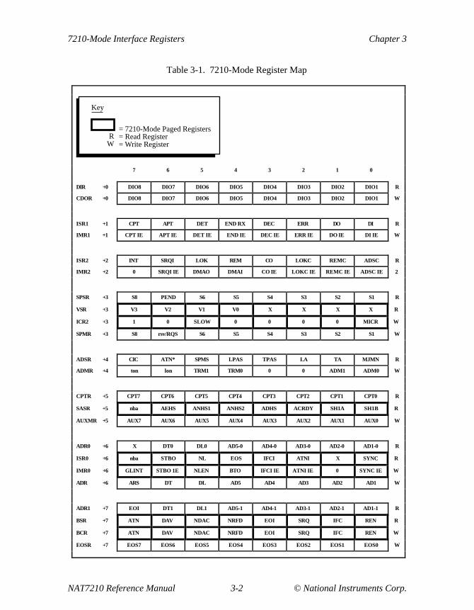
Table 3-1 is the register bit map for the NAT7210 in 7210 mode.
Notice that bold-ruled cells distinguish seven registers that are accessible only when thePage-In state is true. Refer to The Page-In State section that immediately follows theregister map for more information.
7210-Mode Interface Registers Chapter 3
NAT7210 Reference Manual 3-2 © National Instruments Corp.
Table 3-1. 7210-Mode Register Map
Key
= 7210-Mode Paged Registers= Read Register= Write Register
RW
7 6 5 4 3 2 1 0
DIR +0 DIO8 DIO7 DIO6 DIO5 DIO4 DIO3 DIO2 DIO1 R
CDOR +0 DIO8 DIO7 DIO6 DIO5 DIO4 DIO3 DIO2 DIO1 W
ISR1 +1 CPT APT DET END RX DEC ERR DO DI R
IMR1 +1 CPT IE APT IE DET IE END IE DEC IE ERR IE DO IE DI IE W
ISR2 +2 INT SRQI LOK REM CO LOKC REMC ADSC R
IMR2 +2 0 SRQI IE DMAO DMAI CO IE LOKC IE REMC IE ADSC IE 2
SPSR +3 S8 PEND S6 S5 S4 S3 S2 S1 R
VSR +3 V3 V2 V1 V0 X X X X R
ICR2 +3 1 0 SLOW 0 0 0 0 MICR W
SPMR +3 S8 rsv/RQS S6 S5 S4 S3 S2 S1 W
ADSR +4 CIC ATN* SPMS LPAS TPAS LA TA MJMN R
ADMR +4 ton lon TRM1 TRM0 0 0 ADM1 ADM0 W
CPTR +5 CPT7 CPT6 CPT5 CPT4 CPT3 CPT2 CPT1 CPT0 R
SASR +5 nba AEHS ANHS1 ANHS2 ADHS ACRDY SH1A SH1B R
AUXMR +5 AUX7 AUX6 AUX5 AUX4 AUX3 AUX2 AUX1 AUX0 W
ADR0 +6 X DT0 DL0 AD5-0 AD4-0 AD3-0 AD2-0 AD1-0 R
ISR0 +6 nba STBO NL EOS IFCI ATNI X SYNC R
IMR0 +6 GLINT STBO 1E NLEN BTO IFCI IE ATNI IE 0 SYNC IE W
ADR +6 ARS DT DL AD5 AD4 AD3 AD2 AD1 W
ADR1 +7 EOI DT1 DL1 AD5-1 AD4-1 AD3-1 AD2-1 AD1-1 R
BSR +7 ATN DAV NDAC NRFD EOI SRQ IFC REN R
BCR +7 ATN DAV NDAC NRFD EOI SRQ IFC REN W
EOSR +7 EOS7 EOS6 EOS5 EOS4 EOS3 EOS2 EOS1 EOS0 W
Chapter 3 7210-Mode Interface Registers
© National Instruments Corp. 3-3 NAT7210 Reference Manual
The Page-In State
At some offsets, Table 3-1 shows two readable or two writable registers. The shadedregisters in Table 3-1 are accessible only when the Page-In state is true. For each shadedregister, the corresponding unshaded register is accessible only when the Page-In state isfalse.
How to Page-In
The NAT7210 enters the Page-In state when the host interface writes the Page-Inauxiliary command to the Auxiliary Mode Register (AUXMR). The NAT7210 registersappear at their Page-In state offset for the first register access after the Page-In command.The NAT7210 leaves the Page-In state at the end of the first register access after thePage-In command.
Hidden Registers
In addition to the registers shown in Table 3-1, the NAT7210 contains hidden registers.All hidden registers are write-only registers. Two or more hidden registers can appear atthe same offset. When you write an 8-bit pattern to these offsets, some of the bitsdetermine which hidden register will be written. The other bits represent the valuewritten to the register.
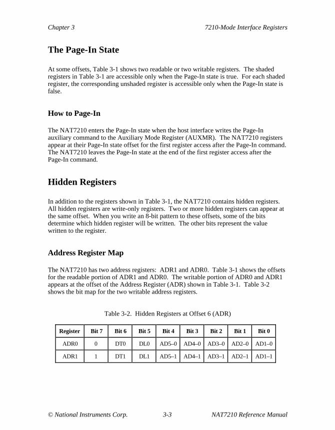
Address Register Map
The NAT7210 has two address registers: ADR1 and ADR0. Table 3-1 shows the offsetsfor the readable portion of ADR1 and ADR0. The writable portion of ADR0 and ADR1appears at the offset of the Address Register (ADR) shown in Table 3-1. Table 3-2shows the bit map for the two writable address registers.
Table 3-2. Hidden Registers at Offset 6 (ADR)
Register Bit 7 Bit 6 Bit 5 Bit 4 Bit 3 Bit 2 Bit 1 Bit 0
ADR0 0 DT0 DL0 AD5–0 AD4–0 AD3–0 AD2–0 AD1–0
ADR1 1 DT1 DL1 AD5–1 AD4–1 AD3–1 AD2–1 AD1–1

7210-Mode Interface Registers Chapter 3
NAT7210 Reference Manual 3-4 © National Instruments Corp.
Auxiliary Mode Register Map
Several hidden registers appear at the AUXMR offset. Table 3-3 shows these hiddenregisters.
Table 3-3. Hidden Registers at Offset 5 (AUXMR)
Register Bit 7 Bit 6 Bit 5 Bit 4 Bit 3 Bit 2 Bit 1 Bit 0
PPR 0 1 1 U S P 3 P 2 P 1
AUXRA 1 0 0 BIN XEOS REOS HLDE HLDA
AUXRB 1 0 1 ISS INV TRI SPEOI CPTENABLE
AUXRE 1 1 0 0 DHADT DHADC DHDT DHDC
AUXRF 1 1 0 1 DHATA DHALA DHUNTL DHALL
AUXRG 0 1 0 0 NTNL RPP2 DISTCT CHES
AUXRI 1 1 1 0 USTD PP2 0 SISB
ICR 0 0 1 0 F 3 F 2 F 1 F 0
Register Bit Descriptions
Some 7210-mode registers and 9914-mode registers share identical names. The9914-mode registers are described in Chapter 4, 9914-Mode Interface Registers . If youare using the NAT7210 in 7210 mode, be sure to read the proper description for the7210-mode registers.
All registers are listed in alphabetical order. The registers are alphabetized according totheir mnemonics.

Chapter 3 7210-Mode Interface Registers
© National Instruments Corp. 3-5 NAT7210 Reference Manual
Address Mode Register (ADMR)
Attributes: Write only
7 6 5 4 3 2 1 0
ton lon TRM1 TRM0 0 0 ADM1 ADM0
The host interface can put the NAT7210 into one of six GPIB addressing modes bywriting to the Address Mode Register (ADMR). The values of ADMR (7–6; 3–0) areundefined after a hardware reset. Before the host interface can clear pon, it must write avalid pattern to the ADMR.
Table 3-4. Valid ADMR Patterns
Hex Valueof
ADMR*
GPIB Addressing Mode
30 No Addressing
The Controller cannot address the NAT7210 to become a Talker orListener in no-addressing mode.
31 Normal Dual Addressing
The NAT7210 can implement one or two logical devices by usingnormal dual addressing.
See the GPIB Addressing section in Chapter 5, Software Considerations .
32 Extended Single Addressing
Extended single addressing mode implements the Extended Listener andExtended Talker functions, as defined in the IEEE 488 standard, withoutintervention from the host interface.
See the GPIB Addressing section in Chapter 5, Software Considerations .
33 Extended Dual Addressing
Extended dual addressing mode implements the Extended Listener andExtended Talker functions, as defined in the IEEE 488 standard. Thismode requires intervention from the host interface.
See the GPIB Addressing section in Chapter 5, Software Considerations .
(continues)

7210-Mode Interface Registers Chapter 3
NAT7210 Reference Manual 3-6 © National Instruments Corp.
ADMR (continued)
Table 3-4. Valid ADMR Patterns (Continued)
Hex Valueof
ADMR*
GPIB Addressing Mode
70 Listen Only (lon)
The NAT7210 becomes a GPIB Listener and enters the Listener ActiveState (LACS). Do not use lon if a GPIB Controller is present in theGPIB system.
The host interface should write a hex 30 (No Addressing) to the ADMRimmediately after writing lon to the ADMR. To force the NAT7210 toexit LACS, issue the unlisten (lul) auxiliary command.
B0 Talk Only (ton)
The NAT7210 becomes a GPIB Talker. Do not use ton if a GPIBController is present in the GPIB system.
The host interface should write a hex 30 (No Addressing) to the ADMRimmediately after writing ton to the ADMR. To force the NAT7210 toexit TACS, issue the local untalk (lut) auxiliary command.
* The hex values in Table 3-4 assume that TRM1 = 1 and TRM0 = 1.

Chapter 3 7210-Mode Interface Registers
© National Instruments Corp. 3-7 NAT7210 Reference Manual
ADMR (continued)
Bit Mnemonic Description
5–4w TRM[1–0] Transmit/Receive Mode bit
TRM1 and TRM0 control the function of the NAT7210T/R2 and T/R3 output pins in the following manner:
TRM1 TRM0 T/R2 T/R3
0 0 EOIOE TRIG
0 1 CIC TRIG
1 0 CIC EOIOE
1 1 CIC PE
Key:
EOIOE = GPIB EOI signal output enableTACS + SPAS + CIC & ~(CSBS +CSHS)
CIC = Controller-in-Charge (CIDS + CADS)TRIG = Trigger (pulses when DTAS = 1 or a
trigger auxiliary command is issued)PE = Pull-up enable (CIC + -(PPAS))
A hardware reset clears TRM1 and TRM0.
Note: In many applications, the NAT7210 isinterfaced to a 75160 and a 75162 GPIBtransceiver. In these applications, TRM1 andTRM0 should always be set.

7210-Mode Interface Registers Chapter 3
NAT7210 Reference Manual 3-8 © National Instruments Corp.
Address Register (ADR)
Attributes: Write only
7 6 5 4 3 2 1 0
ARS DT DL AD5 AD4 AD3 AD2 AD1
Writing to the Address Register (ADR) loads the internal registers ADR0 and ADR1.You must load both ADR0 and ADR1 for all addressing modes. See the GPIBAddressing section in Chapter 5, Software Considerations.
Bit Mnemonic Description
7w ARS Address Register Select bit
If ARS = 1, writing to the ADR loads the seven low-orderbits of ADR into internal register ADR1. If ARS = 0,writing to the ADR loads the seven low-order bits intoADR0.
6w DT Disable Talker bit
DT = 1 disables recognition of the GPIB talk addressformed from AD[5–1]. ADR0 and ADR1 haveindependent DT bits.
5w DL Disable Listener bit
DL = 1 disables recognition of the GPIB listen addressformed from AD[5–1]. ADR0 and ADR1 haveindependent DL bits.
4–0w AD[5–1] NAT7210 GPIB Address bits 5 through 1
These bits specify the GPIB address of the NAT7210.The corresponding GPIB talk address is formed by addinghex 40 to AD[5–1], while the corresponding GPIB listenaddress is formed by adding hex 20 to AD[5–1]. Thevalue written to AD[5–1] should not be 11111 (binary),because the corresponding talk and listen addresses wouldconflict with the GPIB Untalk (UNT) and GPIB Unlisten(UNL) commands.
ADR0 and ADR1 have independent AD[5–1] bits.

Chapter 3 7210-Mode Interface Registers
© National Instruments Corp. 3-9 NAT7210 Reference Manual
Address Register 0 (ADR0)
Attributes: Read only
7 6 5 4 3 2 1 0
X DT0 DL0 AD5–0 AD4–0 AD3–0 AD2–0 AD1–0
Address Register 0 (ADR0) reflects the internal GPIB address status of the NAT7210. Inextended single addressing mode, ADR0 indicates the address and enable bits for theprimary GPIB address of the NAT7210. In the dual primary addressing modes, ADR0indicates the NAT7210 major primary GPIB address. See the GPIB Addressing sectionin Chapter 5, Software Considerations.
Bit Mnemonic Description
7r X Reads back a 1 or 0.
6r DT0 Disable Talker 0 bit
If DT0 = 1, the primary (or major) Talker function is notenabled, and ADR0 is not compared with GPIB Talkeraddresses.
If DT0 = 0, the NAT7210 responds to a GPIB talk addressmatching bits AD[5–0 through 1–0].
5r DL0 Disable Listener 0 bit
If DL0 = 1, the primary (or major) Listener function is notenabled, and ADR0 is not compared with GPIB Listeneraddresses.
If DL0 = 0, the NAT7210 responds to a GPIB listenaddress matching bits AD[5–0 through 1–0].
4–0r AD[5–0 – 1–0] NAT7210 GPIB Address bits 5–0 through 1–0
These are the lower 5 bits of the NAT7210 GPIB primary(or major) address. The primary talk address is formed byadding hex 40 to AD[5–0 through 1–0], while the primarylisten address is formed by adding hex 20.

7210-Mode Interface Registers Chapter 3
NAT7210 Reference Manual 3-10 © National Instruments Corp.
Address Register 1 (ADR1)
Attributes: Read only
7 6 5 4 3 2 1 0
EOI DT1 DL1 AD5–1 AD4–1 AD3–1 AD2–1 AD1–1
Address Register 1 (ADR1) indicates the status of the GPIB address and enable bits forthe secondary address of the NAT7210 if extended single addressing is used. ADR1indicates the minor primary address of the NAT7210 if dual primary addressing is used.See the GPIB Addressing section in Chapter 5, Software Considerations.
Bit Mnemonic Description
7r EOI End-or-Identify bit
EOI indicates the value of the GPIB EOI line that islatched when a data byte is received by the NAT7210GPIB Acceptor Handshake (AH) function. If EOI = 1, theEOI line was asserted with the received byte. EOI iscleared by issuing the Chip Reset auxiliary command.EOI is updated after each byte is received.
6r DT1 Disable Talker 1 bit
If DT1 = 1, the secondary (or minor) Talker function isnot enabled—that is, the GPIB secondary address (orminor primary talk address) is not compared with thisregister.
5r DL1 Disable Listener 1 bit
If DL1 = 1, the secondary (or minor) Listener function isnot enabled—that is, the GPIB secondary address (orminor primary listen address) is not compared with thisregister.
4–0r AD[5–1 – 1–1] NAT7210 GPIB Address bits 5–1 through 1–1
These bits indicate the NAT7210 secondary or minoraddress. Form the secondary address by adding hex 60 tobits AD[5–1 through 1–1]. Form the minor talk addressby adding hex 40 to AD[5–1 through 1–1]. Form thelisten address by adding a hex 20.

Chapter 3 7210-Mode Interface Registers
© National Instruments Corp. 3-11 NAT7210 Reference Manual
Address Status Register (ADSR)
Attributes: Read only
7 6 5 4 3 2 1 0
CIC ATN* SPMS LPAS TPAS LA TA MJMN
The Address Status Register (ADSR) contains information that you can use to monitorthe NAT7210 GPIB address status.
Bit Mnemonic Description
7r CIC Controller-In-Charge bit
CIC = ~(CIDS + CADS)
CIC indicates that the NAT7210 GPIB Controllerfunction is either in an active state with ATN* asserted ora standby state with ATN* unasserted. The Controllerfunction is in an idle state (CIDS or CADS) if CIC = 0.
6r ATN* Attention* bit
ATN* is a status bit that indicates the current level of theGPIB ATN* signal. If ATN* = 0, the GPIB ATN* signalis asserted.
5r SPMS Serial Poll Mode State bit
If SPMS = 1, the NAT7210 GPIB Talker (T) or TalkerExtended (TE) function is enabled to participate in a serialpoll.
SPMS is set bySPE & ACDS
SPMS is cleared by(SPD & ACDS) + pon + IFC
7210-Mode Interface Registers Chapter 3
NAT7210 Reference Manual 3-12 © National Instruments Corp.
ADSR (continued)
Bit Mnemonic Description
4r LPAS Listener Primary Addressed State bit
LPAS indicates that the NAT7210 has received itsprimary listen address. See the Address Mode Register(ADMR) section in this chapter.
LPAS is cleared by(PCG & ~MLA & ACDS) + pon
3r TPAS Talker Primary Addressed State bit
TPAS indicates that the NAT7210 has received itsprimary GPIB talk address. See the Address ModeRegister (ADMR) section in this chapter.
TPAS is cleared by(PCG & ~MTA & ACDS) + pon
2r LA Listener Active bit
LA = 1 when the NAT7210 has been addressed orprogrammed as a GPIB Listener—that is, the NAT7210 isin the Listener Active State (LACS) or the ListenerAddressed State (LADS). The NAT7210 is addressed tolisten when it receives its listen address from the CIC.The NAT7210 can also be programmed to listen by usingthe Listen-Only (lon) bit in the ADMR.
If the NAT7210 is addressed to talk, it is automaticallyunaddressed to listen.
LA is also cleared by(UNL & ACDS) + IFC + pon + (lun & CACS)+ lul
1r TA Talker Active bit
TA = 1 when the NAT7210 has been addressed orprogrammed as the GPIB Talker—that is, the NAT7210 isin the Talker Active State (TACS), the Talker Addressed

Chapter 3 7210-Mode Interface Registers
© National Instruments Corp. 3-13 NAT7210 Reference Manual
ADSR (continued)
Bit Mnemonic Description
State (TADS), or the Serial Poll Active State (SPAS).The NAT7210 can be addressed to talk when it receivesits talk address from the CIC. It can also be programmedto talk by using the Talk-Only (ton) bit in the ADMR.
If the NAT7210 is addressed to listen, it is automaticallyunaddressed to talk.
TA is also cleared by(OTA & ACDS) + IFC + pon + lut
0r MJMN Major-Minor bit
MJMN indicates whether the information in the otherADSR bits applies to the NAT7210 major or minor Talkerand Listener functions. MJMN = 1 when the NAT7210receives its GPIB minor talk address or minor listenaddress. MJMN clears when the NAT7210 receives itsmajor talk or major listen address. The pon message alsoclears MJMN.
Note: Only one Talker or Listener can be active at atime. The MJMN bit indicates which, if either,of the NAT7210 Talker and Listener functions isaddressed or active.
MJMN is always 0 unless the normal or extended dualprimary addressing mode is enabled. See the AddressMode Register (ADMR) section in this chapter.
7210-Mode Interface Registers Chapter 3
NAT7210 Reference Manual 3-14 © National Instruments Corp.
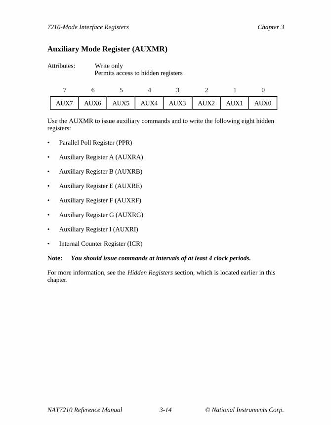
Auxiliary Mode Register (AUXMR)
Attributes: Write onlyPermits access to hidden registers
7 6 5 4 3 2 1 0
AUX7 AUX6 AUX5 AUX4 AUX3 AUX2 AUX1 AUX0
Use the AUXMR to issue auxiliary commands and to write the following eight hiddenregisters:
• Parallel Poll Register (PPR)
• Auxiliary Register A (AUXRA)
• Auxiliary Register B (AUXRB)
• Auxiliary Register E (AUXRE)
• Auxiliary Register F (AUXRF)
• Auxiliary Register G (AUXRG)
• Auxiliary Register I (AUXRI)
• Internal Counter Register (ICR)
Note: You should issue commands at intervals of at least 4 clock periods.
For more information, see the Hidden Registers section, which is located earlier in thischapter.

Chapter 3 7210-Mode Interface Registers
© National Instruments Corp. 3-15 NAT7210 Reference Manual
AUXMR (continued)
Table 3-5 summarizes the AUXMR auxiliary commands and Table 3-6 describes theAUXMR auxiliary commands.
Table 3-5. Auxiliary Command Summary
HexCode*
Auxiliary Command
00 Immediate Execute Power-On (pon)
01 Clear Parallel Poll Flag (~ist)
02 Chip Reset (chip_reset)
03 Finish Handshake (rhdf)
04 Trigger (trig)
05 Clear Or Pulse Return To Local (rtl)
06 Send EOI (seoi)
07 Nonvalid Secondary Command OrAddress (nonvalid)
08† Request Control Command (rqc)
09 Set Parallel Poll Flag (ist)
0A† Release Control Command (rlc)
0B† Untalk Command (lut)
0C† Unlisten Command (lul)
0D Set Return To Local
0E† New Byte Available False (nbaf)
0F Valid Secondary Command or Address(valid)
10 Go To Standby (gts)
(continues)

7210-Mode Interface Registers Chapter 3
NAT7210 Reference Manual 3-16 © National Instruments Corp.
AUXMR (continued)
Table 3-5. Auxiliary Command Summary (Continued)
HexCode*
Auxiliary Command
11121A
Take Control Asynchronously (tca)Take Control Synchronously (tcs)Take Control Synchronously On End (tcse)
131B1C
Listen (ltn)Listen In Continuous Mode (ltn and cont)Local Unlisten (lun)
14 Disable System Control (~rsc)
15† Switch To 9914 Mode Command (sw9914)
161E
Clear IFC (~sic & rsc)Set IFC (sic & rsc)
171F
Clear REN (~sre & rsc)Set REN (sre & rsc)
18†19†
Request rsv True (reqt)Request rsv False (reqf)
1D Execute Parallel Poll (rppl)
50† Page-In Additional Registers (page-in)
51† Holdoff Handshake Immediately (hldi)
54† Clear DET (ISR1[5]r) Command
55† Clear END (ISR1[4]r) Command
56† Clear DEC (ISR1[3]r) Command
57† Clear ERR (ISR1[2]r) Command
58† Clear SRQI (ISR2[6]r) Command
59† Clear LOKC (ISR2[2]r) Command
5A† Clear REMC (ISR2[1]r) Command
(continues)
Chapter 3 7210-Mode Interface Registers
© National Instruments Corp. 3-17 NAT7210 Reference Manual
AUXMR (continued)
Table 3-5. Auxiliary Command Summary (Continued)
HexCode*
Auxiliary Command
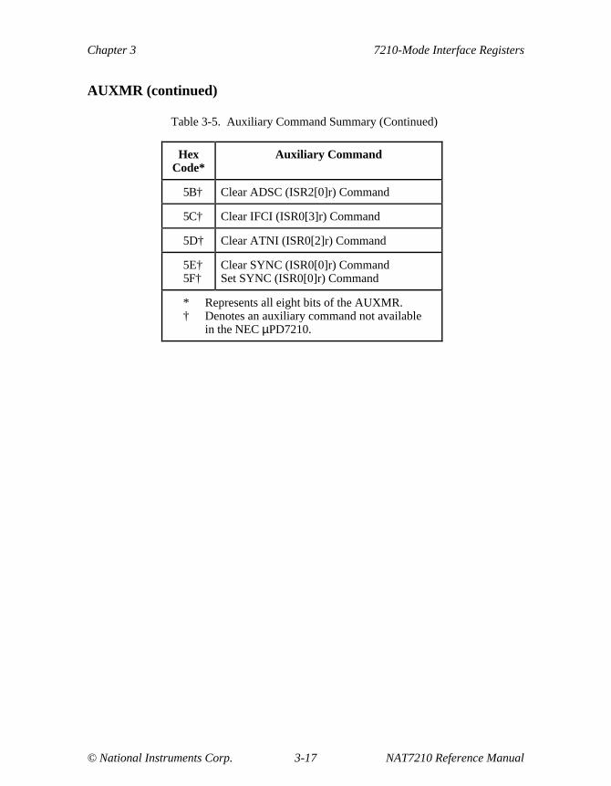
5B† Clear ADSC (ISR2[0]r) Command
5C† Clear IFCI (ISR0[3]r) Command
5D† Clear ATNI (ISR0[2]r) Command
5E†5F†
Clear SYNC (ISR0[0]r) CommandSet SYNC (ISR0[0]r) Command
* Represents all eight bits of the AUXMR.† Denotes an auxiliary command not available
in the NEC µPD7210.

7210-Mode Interface Registers Chapter 3
NAT7210 Reference Manual 3-18 © National Instruments Corp.
AUXMR (continued)
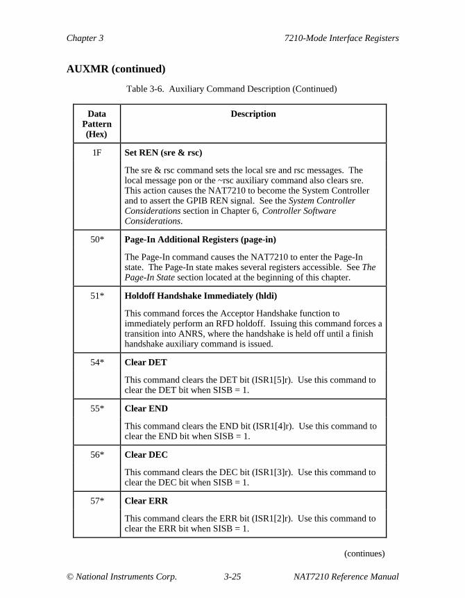
Table 3-6. Auxiliary Command Description
DataPattern(Hex)
Description
00 Immediate Execute Power-On (pon)
The Immediate Execute Power-On auxiliary command sets the localpon message true, then clears it. If the local pon message is alreadyasserted, the pon auxiliary command simply clears the local ponmessage. The following figure illustrates the behavior of the localpon message:
HW reset +chip_reset aux. command
local ponmessage
true
start of pon aux.command pulse
end of pon aux.command pulse
When the local pon message is true, the NAT7210 holds all GPIBinterface functions in their idle states.
0109
Clear Parallel Poll Flag (~ist)Set Parallel Poll Flag (ist)
These commands set and clear the Parallel Poll Flag. The value ofthe Parallel Poll Flag is used as the local message ist whenAUXRB[4]w = 0. The value of SRQS is used as ist when ISS = 1.A hardware reset or the Chip Reset auxiliary command clears ist.
(continues)

Chapter 3 7210-Mode Interface Registers
© National Instruments Corp. 3-19 NAT7210 Reference Manual
AUXMR (continued)
Table 3-6. Auxiliary Command Description (Continued)
DataPattern(Hex)
Description
02 Chip Reset
The Chip Reset auxiliary command resets the NAT7210 to thefollowing conditions:
• The local pon message is set and the interface functions are placed in their idle states.
• The SPMR bits are cleared.
• The TRM[1–0] bits are cleared.
• The EOI bit is cleared.
• The AUXRA, AUXRB, AUXRE, AUXRF, AUXRG, and AUXRI registers are cleared.
• The Parallel Poll Flag is cleared.
• The BCR is cleared.
The interface functions remain in their idle states until they arereleased by an Immediate Execute pon command. While theinterface functions are in their idle states, the host interface canprogram the NAT7210 writable bits to their desired states.
03 Finish Handshake (rhdf)
The Finish Handshake command finishes a GPIB handshake that wasstopped because of a Holdoff On RFD condition.
See The GPIB rdy Message and RFD Holdoffs section in Chapter 5,Software Considerations.
(continues)

7210-Mode Interface Registers Chapter 3
NAT7210 Reference Manual 3-20 © National Instruments Corp.
AUXMR (continued)
Table 3-6. Auxiliary Command Description (Continued)
DataPattern(Hex)
Description
04 Trigger (trig)
The Trigger command generates a high pulse on the T/R 3 pin whenTRM1 = 0. The DET bit is not set by issuing the Trigger command.
050D
Clear Or Pulse Return To Local (rtl)Set Return To Local (rtl)
The two Return To Local commands implement the rtl message asdefined by the IEEE 488 standard. If the host interface writes 05 hex,the rtl message is generated in the form of a pulse. If rtl is alreadyset, the rtl command clears it. If the host interface writes 0D hex, thertl command is set and remains set until either the 05 hex rtlcommand is issued or a Chip Reset auxiliary command is issued.
06 Send EOI (seoi)
The seoi command causes the GPIB End-or-Identify (EOI) line to gotrue with the next data byte transmitted. The EOI line is cleared uponcompletion of the handshake for that byte. When NTNL = 0, theNAT7210 recognizes the seoi command only if TACS = 1—that is,the NAT7210 is in the Talker Active State.
07 Nonvalid Secondary Command Or Address (nonvalid)
The nonvalid command releases a DAC (Data Accepted) holdoff.If APT = 1, the NAT7210 operates as if an Other Secondary Address(OSA) message had been received.
08* Request Control Command (rqc)
If the NAT7210 is in the Idle Controller State, the rqc commandforces the NAT7210 to become the Active Controller when it detectsthat the ATN signal is unasserted.
0A* Release Control Command (rlc)
The rlc command forces the NAT7210 to become an Idle Controllerand to unassert ATN.
(continues)

Chapter 3 7210-Mode Interface Registers
© National Instruments Corp. 3-21 NAT7210 Reference Manual
AUXMR (continued)
Table 3-6. Auxiliary Command Description (Continued)
DataPattern(Hex)
Description
0B* Untalk (lut)
The lut command issues the local unt message, forcing the Talkerfunction to enter TIDS.
0C* Unlisten (lul)
The lul command issues the local unl message, forcing the Listenerfunction to enter LIDS.
0E* New Byte Available False (nbaf)
nbaf forces the local message, nba, to become false. This actionprohibits the NAT7210 from sending the last byte written to theCommand/Data Our Register (CDOR). See the Using nbaf sectionin Chapter 5, Software Considerations .
0F Valid Secondary Command Or Address (valid)
The valid command releases a DAC holdoff. If APT = 1, theNAT7210 operates as if a My Secondary Address (MSA) messagehad been received.
10 Go To Standby (gts)
The gts command pulses the local gts message. If the NAT7210 isthe Active Controller, gts causes the NAT7210 to become theStandby Controller and to unassert the GPIB ATN signal. See theThree Basic Controller States section in Chapter 6, ControllerSoftware Considerations.
11 Take Control Asynchronously (tca)
The tca command pulses the local tca message. If the NAT7210 isthe Standby Controller, tca causes the NAT7210 to become theActive Controller and to assert the GPIB ATN signal. See theStandby State to Active State section in Chapter 6, ControllerSoftware Considerations.
(continues)
7210-Mode Interface Registers Chapter 3
NAT7210 Reference Manual 3-22 © National Instruments Corp.
AUXMR (continued)
Table 3-6. Auxiliary Command Description (Continued)
DataPattern(Hex)
Description
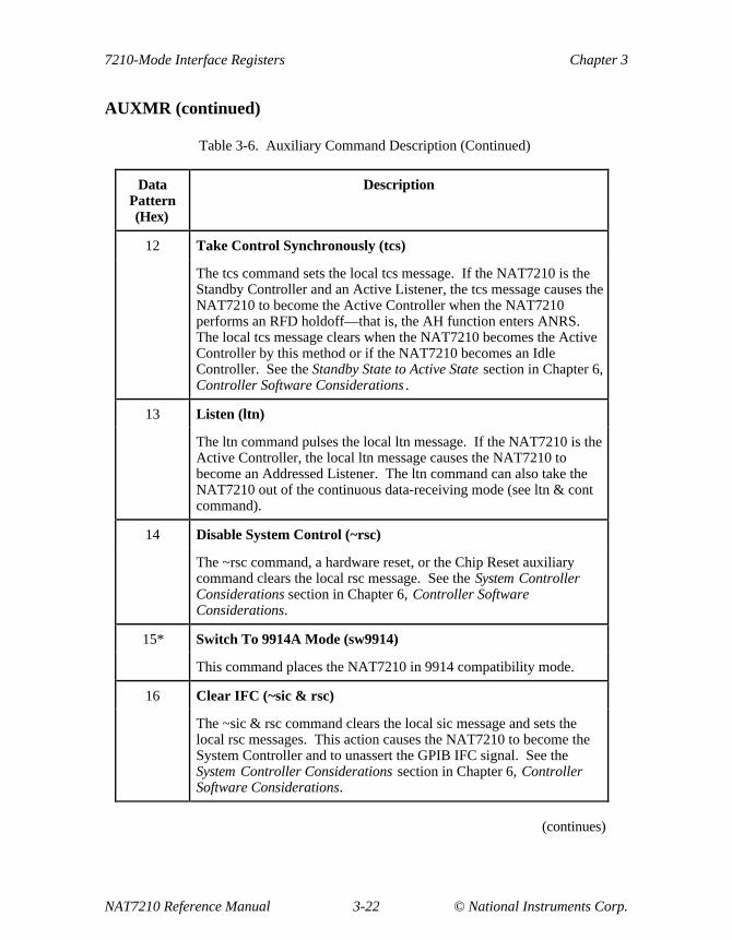
12 Take Control Synchronously (tcs)
The tcs command sets the local tcs message. If the NAT7210 is theStandby Controller and an Active Listener, the tcs message causes theNAT7210 to become the Active Controller when the NAT7210performs an RFD holdoff—that is, the AH function enters ANRS.The local tcs message clears when the NAT7210 becomes the ActiveController by this method or if the NAT7210 becomes an IdleController. See the Standby State to Active State section in Chapter 6,Controller Software Considerations .
13 Listen (ltn)
The ltn command pulses the local ltn message. If the NAT7210 is theActive Controller, the local ltn message causes the NAT7210 tobecome an Addressed Listener. The ltn command can also take theNAT7210 out of the continuous data-receiving mode (see ltn & contcommand).
14 Disable System Control (~rsc)
The ~rsc command, a hardware reset, or the Chip Reset auxiliarycommand clears the local rsc message. See the System ControllerConsiderations section in Chapter 6, Controller SoftwareConsiderations.
15* Switch To 9914A Mode (sw9914)
This command places the NAT7210 in 9914 compatibility mode.
16 Clear IFC (~sic & rsc)
The ~sic & rsc command clears the local sic message and sets thelocal rsc messages. This action causes the NAT7210 to become theSystem Controller and to unassert the GPIB IFC signal. See theSystem Controller Considerations section in Chapter 6, ControllerSoftware Considerations.
(continues)
Chapter 3 7210-Mode Interface Registers
© National Instruments Corp. 3-23 NAT7210 Reference Manual
AUXMR (continued)
Table 3-6. Auxiliary Command Description (Continued)
DataPattern(Hex)
Description
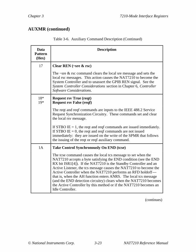
17 Clear REN (~sre & rsc)
The ~sre & rsc command clears the local sre message and sets thelocal rsc messages. This action causes the NAT7210 to become theSystem Controller and to unassert the GPIB REN signal. See theSystem Controller Considerations section in Chapter 6, ControllerSoftware Considerations.
18*19*
Request rsv True (reqt)Request rsv False (reqf)
The reqt and reqf commands are inputs to the IEEE 488.2 ServiceRequest Synchronization Circuitry. These commands set and clearthe local rsv message.
If STBO IE = 1, the reqt and reqf commands are issued immediately.If STBO IE = 0, the reqt and reqf commands are not issuedimmediately: they are issued on the write of the SPMR that followsthe issuing of the reqt or reqf auxiliary command.
1A Take Control Synchronously On END (tcse)
The tcse command causes the local tcs message to set when theNAT7210 accepts a byte satisfying the END condition (see the ENDRX bit ISR1[4]). If the NAT7210 is the Standby Controller and anActive Listener, the tcs message causes the NAT7210 to become theActive Controller when the NAT7210 performs an RFD holdoff—that is, when the AH function enters ANRS. The local tcs message(and the END detection circuitry) clears when the NAT7210 becomesthe Active Controller by this method or if the NAT7210 becomes anIdle Controller.
(continues)

7210-Mode Interface Registers Chapter 3
NAT7210 Reference Manual 3-24 © National Instruments Corp.
AUXMR (continued)
Table 3-6. Auxiliary Command Description (Continued)
DataPattern(Hex)
Description
1B Listen In Continuous Mode (ltn & cont)
The ltn & cont command pulses the local ltn message. If theNAT7210 is the Active Controller, the local ltn message causes theNAT7210 to become an Addressed Listener.
The ltn & cont command also places the NAT7210 in continuousmode regardless of the settings of the AUXRA[1–0] bits (see TheGPIB rdy Message and RFD Holdoffs section in Chapter 5). Ifthe NAT7210 enters continuous mode because of the ltn & contcommand, it remains in continuous mode until the NAT7210becomes unaddressed to Listen—that is, the L or LE function entersLIDS—or until the control program issues the ltn command.
1C Local Unlisten (lun)
The lun command pulses the local lun message. If the NAT7210 isthe Active Controller, the local lun message causes the NAT7210 tobecome an Unaddressed Listener—that is, the L or LE function entersLIDS.
1D Execute Parallel Poll (rpp1)
The rpp1 command sets the local rpp message. If the NAT7210 isthe Active Controller, the rpp message causes the NAT7210 to sendthe IDY message to all GPIB devices in the system and to conducta parallel poll. (See the Conducting Parallel Polls section inChapter 6.) The rpp message clears when the NAT7210 completesa parallel poll or becomes an Idle Controller.
1E Set IFC (sic & rsc)
The sic & rsc command sets the local sic and rsc messages. The localmessage pon or the ~rsc auxiliary command also clears sic. Thisaction causes the NAT7210 to become the System Controller and toassert the GPIB IFC signal. See the System ControllerConsiderations section in Chapter 6, Controller SoftwareConsiderations.
(continues)
Chapter 3 7210-Mode Interface Registers
© National Instruments Corp. 3-25 NAT7210 Reference Manual
AUXMR (continued)
Table 3-6. Auxiliary Command Description (Continued)
DataPattern(Hex)
Description
1F Set REN (sre & rsc)
The sre & rsc command sets the local sre and rsc messages. Thelocal message pon or the ~rsc auxiliary command also clears sre.This action causes the NAT7210 to become the System Controllerand to assert the GPIB REN signal. See the System ControllerConsiderations section in Chapter 6, Controller SoftwareConsiderations.
50* Page-In Additional Registers (page-in)
The Page-In command causes the NAT7210 to enter the Page-Instate. The Page-In state makes several registers accessible. See ThePage-In State section located at the beginning of this chapter.
51* Holdoff Handshake Immediately (hldi)
This command forces the Acceptor Handshake function toimmediately perform an RFD holdoff. Issuing this command forces atransition into ANRS, where the handshake is held off until a finishhandshake auxiliary command is issued.
54* Clear DET
This command clears the DET bit (ISR1[5]r). Use this command toclear the DET bit when SISB = 1.
55* Clear END
This command clears the END bit (ISR1[4]r). Use this command toclear the END bit when SISB = 1.
56* Clear DEC
This command clears the DEC bit (ISR1[3]r). Use this command toclear the DEC bit when SISB = 1.
57* Clear ERR
This command clears the ERR bit (ISR1[2]r). Use this command toclear the ERR bit when SISB = 1.
(continues)

7210-Mode Interface Registers Chapter 3
NAT7210 Reference Manual 3-26 © National Instruments Corp.
AUXMR (continued)
Table 3-6. Auxiliary Command Description (Continued)
DataPattern(Hex)
Description
58* Clear SRQI Command
This command clears the SRQI bit if SISB = 1. See the SRQI bitdescription that is in the Interrupt Status Register 2 (ISR2) section inthis chapter.
59* Clear LOKC
This command clears the LOKC bit (ISR2[2]r). Use this command toclear the LOKC bit when SISB = 1.
5A* Clear REMC
This command clears the REMC bit (ISR2[1]r). Use this commandto clear the REMC bit when SISB = 1.
5B* Clear ADSC
This command clears the ADSC bit (ISR2[0]r). Use this command toclear the ADCS bit when SISB = 1.
5C* Clear IFCI
This command clears the IFCI bit (ISR0[3]r). Use this command toclear the IFCI bit when SISB = 1.
5D* Clear ATNI
This command clears the ATNI bit (ISR0[2]r). Use this command toclear the ATNI bit when SISB = 1.
5E*5F*
Clear SYNCSet SYNC
These commands start or reset the SYNC function.
* Denotes an auxiliary command not available in the µPD7210.

Chapter 3 7210-Mode Interface Registers
© National Instruments Corp. 3-27 NAT7210 Reference Manual
Auxiliary Register A (AUXRA)
Attributes: Write onlyAccessed at the same offset as AUXMR
7 6 5 4 3 2 1 0
1 0 0 BIN XEOS REOS HLDE HLDA
AUXRA controls the End-of-String (EOS) and END messages and specifies the RFDholdoff mode. The Chip Reset auxiliary command or a hardware reset clears AUXRA.You write to AUXRA at the same offset as the AUXMR.
Bit Mnemonic Description
4w BIN Binary bit
The BIN bit selects the length of the EOS message. IfBIN = 1, the End-of-String Register (EOSR) is treated asan 8-bit byte. When BIN = 0, the EOSR is treated as a7-bit register (for ASCII characters), and only a 7-bitcomparison is done with the data on the GPIB.
3w XEOS Transmit END With EOS bit
XEOS permits or prohibits automatic transmission of theGPIB END message at the same time as the EOS messagewhen the NAT7210 is in TACS. If XEOS = 1 and thebyte in the CDOR matches the contents of the EOSR, theEOI line is sent true along with the data.
2w REOS END On EOS Received bit
The REOS bit permits or prohibits setting the END bit(ISR1[4]r) when the NAT7210 receives the EOS messageas a Listener. If REOS = 1 and the byte in the DIRmatches the byte in the EOSR, the END RX bit(ISR1[4]r) is set and the acceptor function treats the EOScharacter just as if it were received with EOI asserted.
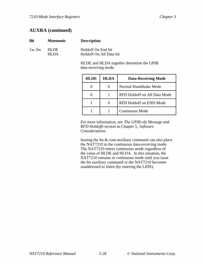
7210-Mode Interface Registers Chapter 3
NAT7210 Reference Manual 3-28 © National Instruments Corp.
AUXRA (continued)
Bit Mnemonic Description
1w, 0w HLDE Holdoff On End bitHLDA Holdoff On All Data bit
HLDE and HLDA together determine the GPIBdata-receiving mode.
HLDE HLDA Data-Receiving Mode
0 0 Normal Handshake Mode
0 1 RFD Holdoff on All Data Mode
1 0 RFD Holdoff on END Mode
1 1 Continuous Mode
For more information, see The GPIB rdy Message andRFD Holdoffs section in Chapter 5, SoftwareConsiderations.
Issuing the ltn & cont auxiliary command can also placethe NAT7210 in the continuous data-receiving mode.The NAT7210 enters continuous mode regardless ofthe value of HLDE and HLDA. In this situation, theNAT7210 remains in continuous mode until you issuethe ltn auxiliary command or the NAT7210 becomesunaddressed to listen (by entering the LIDS).
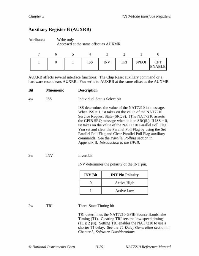
Chapter 3 7210-Mode Interface Registers
© National Instruments Corp. 3-29 NAT7210 Reference Manual
Auxiliary Register B (AUXRB)
Attributes: Write onlyAccessed at the same offset as AUXMR
7 6 5 4 3 2 1 0
1 0 1 ISS INV TRI SPEOI CPTENABLE
AUXRB affects several interface functions. The Chip Reset auxiliary command or ahardware reset clears AUXRB. You write to AUXRB at the same offset as the AUXMR.
Bit Mnemonic Description
4w ISS Individual Status Select bit
ISS determines the value of the NAT7210 ist message.When ISS = 1, ist takes on the value of the NAT7210Service Request State (SRQS). (The NAT7210 assertsthe GPIB SRQ message when it is in SRQS.) If ISS = 0,ist takes on the value of the NAT7210 Parallel Poll Flag.You set and clear the Parallel Poll Flag by using the SetParallel Poll Flag and Clear Parallel Poll Flag auxiliarycommands. See the Parallel Polling section inAppendix B, Introduction to the GPIB.
3w INV Invert bit
INV determines the polarity of the INT pin.
INV Bit INT Pin Polarity
0 Active High
1 Active Low
2w TRI Three-State Timing bit
TRI determines the NAT7210 GPIB Source HandshakeTiming (T1). Clearing TRI sets the low-speed timing(T1 ≥ 2 µs). Setting TRI enables the NAT7210 to use ashorter T1 delay. See the T1 Delay Generation section inChapter 5, Software Considerations.

7210-Mode Interface Registers Chapter 3
NAT7210 Reference Manual 3-30 © National Instruments Corp.
AUXRB (continued)
Bit Mnemonic Description
1w SPEOI Send Serial Poll EOI bit
SPEOI determines whether the NAT7210 sends EOIwhen a Controller serial polls the NAT7210.
SPEOI EOI During Serial Polls
0 Sent False
1 Sent True
0w CPT ENABLE Command Pass Through Enable bit
The CPT ENABLE bit permits or prohibits detectingundefined GPIB commands and permits or prohibitssetting the CPT bit (ISR1[7]r).
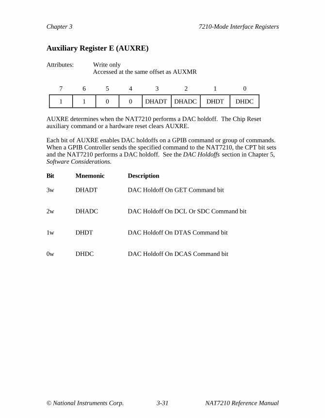
Chapter 3 7210-Mode Interface Registers
© National Instruments Corp. 3-31 NAT7210 Reference Manual
Auxiliary Register E (AUXRE)
Attributes: Write onlyAccessed at the same offset as AUXMR
7 6 5 4 3 2 1 0
1 1 0 0 DHADT DHADC DHDT DHDC
AUXRE determines when the NAT7210 performs a DAC holdoff. The Chip Resetauxiliary command or a hardware reset clears AUXRE.
Each bit of AUXRE enables DAC holdoffs on a GPIB command or group of commands.When a GPIB Controller sends the specified command to the NAT7210, the CPT bit setsand the NAT7210 performs a DAC holdoff. See the DAC Holdoffs section in Chapter 5,Software Considerations.
Bit Mnemonic Description
3w DHADT DAC Holdoff On GET Command bit
2w DHADC DAC Holdoff On DCL Or SDC Command bit
1w DHDT DAC Holdoff On DTAS Command bit
0w DHDC DAC Holdoff On DCAS Command bit
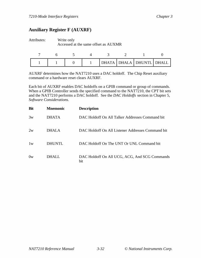
7210-Mode Interface Registers Chapter 3
NAT7210 Reference Manual 3-32 © National Instruments Corp.
Auxiliary Register F (AUXRF)
Attributes: Write onlyAccessed at the same offset as AUXMR
7 6 5 4 3 2 1 0
1 1 0 1 DHATA DHALA DHUNTL DHALL
AUXRF determines how the NAT7210 uses a DAC holdoff. The Chip Reset auxiliarycommand or a hardware reset clears AUXRF.
Each bit of AUXRF enables DAC holdoffs on a GPIB command or group of commands.When a GPIB Controller sends the specified command to the NAT7210, the CPT bit setsand the NAT7210 performs a DAC holdoff. See the DAC Holdoffs section in Chapter 5,Software Considerations.
Bit Mnemonic Description
3w DHATA DAC Holdoff On All Talker Addresses Command bit
2w DHALA DAC Holdoff On All Listener Addresses Command bit
1w DHUNTL DAC Holdoff On The UNT Or UNL Command bit
0w DHALL DAC Holdoff On All UCG, ACG, And SCG Commandsbit
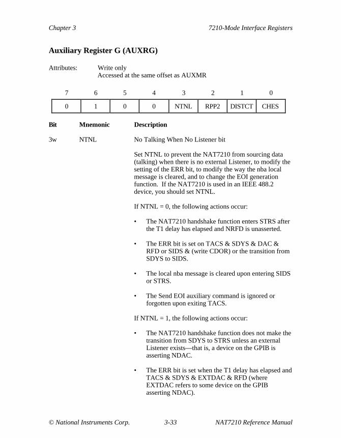
Chapter 3 7210-Mode Interface Registers
© National Instruments Corp. 3-33 NAT7210 Reference Manual
Auxiliary Register G (AUXRG)
Attributes: Write onlyAccessed at the same offset as AUXMR
7 6 5 4 3 2 1 0
0 1 0 0 NTNL RPP2 DISTCT CHES
Bit Mnemonic Description
3w NTNL No Talking When No Listener bit
Set NTNL to prevent the NAT7210 from sourcing data(talking) when there is no external Listener, to modify thesetting of the ERR bit, to modify the way the nba localmessage is cleared, and to change the EOI generationfunction. If the NAT7210 is used in an IEEE 488.2device, you should set NTNL.
If NTNL = 0, the following actions occur:
• The NAT7210 handshake function enters STRS afterthe T1 delay has elapsed and NRFD is unasserted.
• The ERR bit is set on TACS & SDYS & DAC &RFD or SIDS & (write CDOR) or the transition fromSDYS to SIDS.
• The local nba message is cleared upon entering SIDSor STRS.
• The Send EOI auxiliary command is ignored orforgotten upon exiting TACS.
If NTNL = 1, the following actions occur:
• The NAT7210 handshake function does not make thetransition from SDYS to STRS unless an externalListener exists—that is, a device on the GPIB isasserting NDAC.
• The ERR bit is set when the T1 delay has elapsed andTACS & SDYS & EXTDAC & RFD (whereEXTDAC refers to some device on the GPIBasserting NDAC).
7210-Mode Interface Registers Chapter 3
NAT7210 Reference Manual 3-34 © National Instruments Corp.
AUXRG (continued)
Bit Mnemonic Description
• The local nba message is cleared upon entering STRSand ~SPAS.
• The Send EOI auxiliary command is cleared uponentering SDYS or STRS.
2w RPP2 Request Parallel Poll 2 bit
If RPP2 = 1, the local rpp message is true. Clearing RPP2clears rpp. If the NAT7210 is the Active Controller,setting rpp causes the NAT7210 to conduct a parallel poll.See the Conducting Parallel Polls section in Chapter 6,Controller Software Considerations.
1w DISTCT Disable Automatic Take Control bit
If DISTCT = 1, the NAT7210 considers the GPIB TCTmessage undefined. If the GPIB Controller tries to passcontrol to the NAT7210, the NAT7210 will not become aController. You usually set DISTCT if the NAT7210 is atalk-only or listen-only device.
If DISTCT = 0, the NAT7210 recognizes TCT. AnotherController may pass control to the NAT7210 withoutsoftware intervention.
0w CHES Clear Holdoff On End Select bit
CHES determines how long the NAT7210 remembers thatit detected an END condition.
If CHES = 0, the NAT7210 remembers the detection ofthe END condition until the host interface issues theRelease Handshake Holdoff auxiliary command.
If CHES = 1, the NAT7210 remembers the detection ofthe END condition until the Release Handshake Holdoffauxiliary command is issued or the DIR is read when theNAT7210 is in the normal handshake holdoff mode—thatis, HLDE and HLDA = 0.
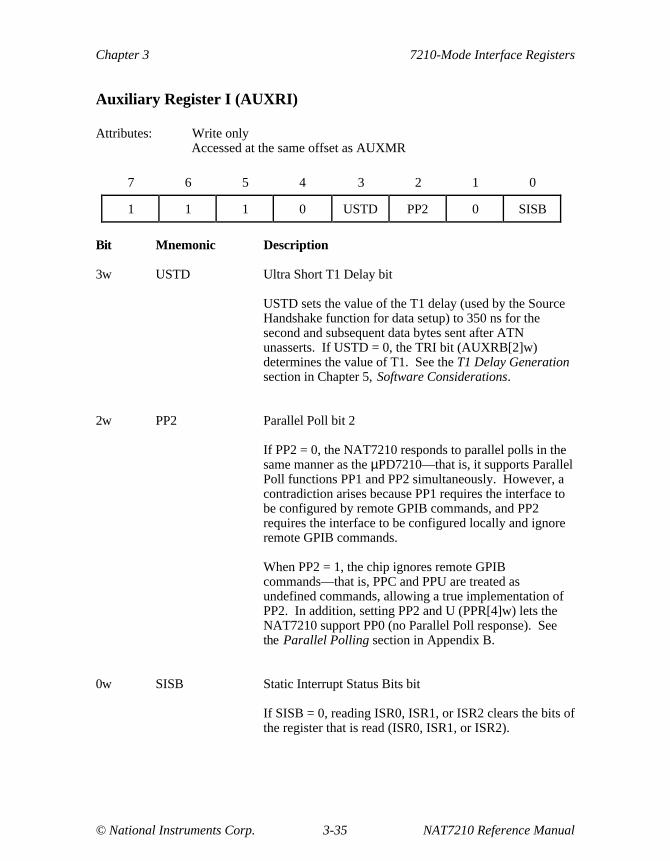
Chapter 3 7210-Mode Interface Registers
© National Instruments Corp. 3-35 NAT7210 Reference Manual
Auxiliary Register I (AUXRI)
Attributes: Write onlyAccessed at the same offset as AUXMR
7 6 5 4 3 2 1 0
1 1 1 0 USTD PP2 0 SISB
Bit Mnemonic Description
3w USTD Ultra Short T1 Delay bit
USTD sets the value of the T1 delay (used by the SourceHandshake function for data setup) to 350 ns for thesecond and subsequent data bytes sent after ATNunasserts. If USTD = 0, the TRI bit (AUXRB[2]w)determines the value of T1. See the T1 Delay Generationsection in Chapter 5, Software Considerations.
2w PP2 Parallel Poll bit 2
If PP2 = 0, the NAT7210 responds to parallel polls in thesame manner as the µPD7210—that is, it supports ParallelPoll functions PP1 and PP2 simultaneously. However, acontradiction arises because PP1 requires the interface tobe configured by remote GPIB commands, and PP2requires the interface to be configured locally and ignoreremote GPIB commands.
When PP2 = 1, the chip ignores remote GPIBcommands—that is, PPC and PPU are treated asundefined commands, allowing a true implementation ofPP2. In addition, setting PP2 and U (PPR[4]w) lets theNAT7210 support PP0 (no Parallel Poll response). Seethe Parallel Polling section in Appendix B.
0w SISB Static Interrupt Status Bits bit
If SISB = 0, reading ISR0, ISR1, or ISR2 clears the bits ofthe register that is read (ISR0, ISR1, or ISR2).

7210-Mode Interface Registers Chapter 3
NAT7210 Reference Manual 3-36 © National Instruments Corp.
AUXRI (continued)
If SISB = 1, the bits remain set until a certain condition ismet. Table 3-7 lists the condition that clears eachinterrupt status bit when SISB = 1.
Table 3-7. Clear Conditions for SISB Bit
Bit Clear Condition when SISB = 1
ADSC pon + clearADSC + ton + lon
APT pon + valid + nonvalid
ATNI pon + clearATNI
CO pon + ~CACS + ~SGNS + nba
CPT pon + read CPTR
DEC pon + clearDEC
DET pon + clearDET
DI pon + (finish handshake) * (Holdoff mode) + read DIR
DO pon + ~TACS + ~SGNS + nba
END pon + clearEND
ERR pon + clearERR
IFCI pon + clearIFCI
LOKC pon + clearLOKC
REMC pon + clearREMC
SRQI pon + clearSRQI
Note: Interrupt Status bits STBO and SYNC are not affected by the SISB bit.
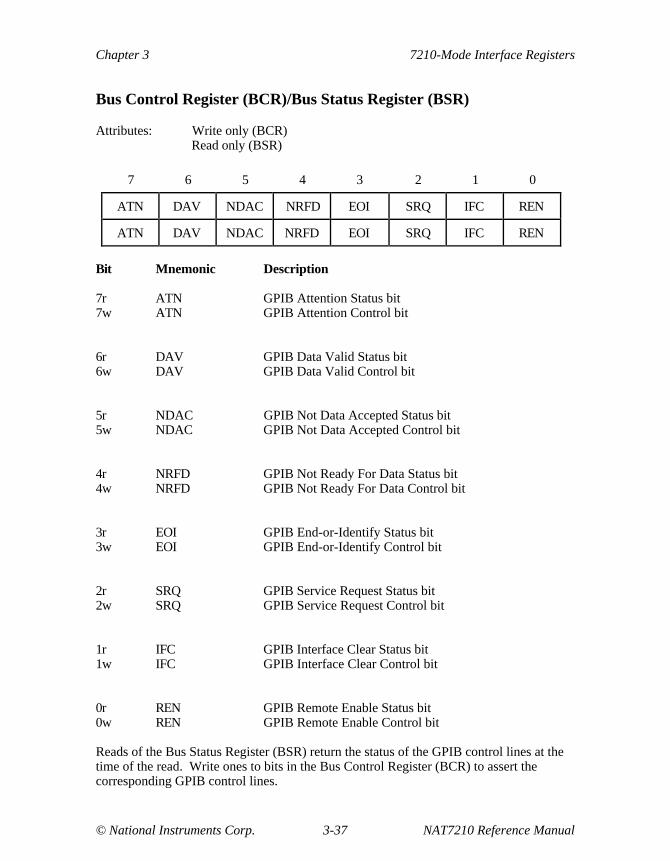
Chapter 3 7210-Mode Interface Registers
© National Instruments Corp. 3-37 NAT7210 Reference Manual
Bus Control Register (BCR)/Bus Status Register (BSR)
Attributes: Write only (BCR)Read only (BSR)
7 6 5 4 3 2 1 0
ATN DAV NDAC NRFD EOI SRQ IFC REN
ATN DAV NDAC NRFD EOI SRQ IFC REN
Bit Mnemonic Description
7r ATN GPIB Attention Status bit7w ATN GPIB Attention Control bit
6r DAV GPIB Data Valid Status bit6w DAV GPIB Data Valid Control bit
5r NDAC GPIB Not Data Accepted Status bit5w NDAC GPIB Not Data Accepted Control bit
4r NRFD GPIB Not Ready For Data Status bit4w NRFD GPIB Not Ready For Data Control bit
3r EOI GPIB End-or-Identify Status bit3w EOI GPIB End-or-Identify Control bit
2r SRQ GPIB Service Request Status bit2w SRQ GPIB Service Request Control bit
1r IFC GPIB Interface Clear Status bit1w IFC GPIB Interface Clear Control bit
0r REN GPIB Remote Enable Status bit0w REN GPIB Remote Enable Control bit
Reads of the Bus Status Register (BSR) return the status of the GPIB control lines at thetime of the read. Write ones to bits in the Bus Control Register (BCR) to assert thecorresponding GPIB control lines.

7210-Mode Interface Registers Chapter 3
NAT7210 Reference Manual 3-38 © National Instruments Corp.
BCR/BSR (continued)
Because the NAT7210 is either transmitting or receiving a GPIB control line at anyparticular time and is not performing both actions simultaneously, setting a bit in theBCR may not automatically assert the corresponding line on the GPIB. If the NAT7210is transmitting a GPIB line when the corresponding bit in the BCR is set, the NAT7210asserts the GPIB line. If the NAT7210 is receiving a GPIB line when the correspondingbit in the BCR is set, the GPIB line is not asserted. However, in both these cases, theGPIB signal internal to the NAT7210 is logically ORed with the value of the BCR bit.Figure 3-1 illustrates the GPIB input/output hardware configuration.
eliminatesglitches inREN & IFC
GPIB Line In
BCR Bit
Transmit Enable
GPIB Line Out
NDAC NRFDSRQ
PIN
Figure 3-1. GPIB I/O Hardware Configuration
In Figure 3-1, Transmit Enable represents the internal signal that is true when the chip isdriving a particular GPIB control line. GPIB Line Out represents the internal signal thatis true when an interface function within the chip is attempting to assert a GPIB controlsignal. BCR Bit corresponds to the bit in the BCR. GPIB Line In represents the internalGPIB lines that are inputs to the GPIB interface functions and the BSR. The internalsignals SRQ , NDAC, and NRFD are monitored by the interface functions even when theyare not driven onto the pin. For this reason, the internal value of these signals is ORedwith the external value.
Because the BSR samples the GPIB control lines from the GPIB transceiver—not theactual GPIB bus—the direction of each line determines the validity of each bit.Generally, when a signal is an input, the BSR reflects its true bus status, while an outputsignal reflects only the NAT7210 value of that particular line. Under normal GPIBoperation, this restriction on the validity of the BSR should not be too limiting, becausethe lines that are typically monitored are valid when they are monitored. For example,the SRQ line is valid in the BSR when the NAT7210 is CIC, which is also when the SRQline will be monitored.

Chapter 3 7210-Mode Interface Registers
© National Instruments Corp. 3-39 NAT7210 Reference Manual
Command/Data Out Register (CDOR)
Attributes: Write only
7 6 5 4 3 2 1 0
DIO8 DIO7 DIO6 DIO5 DIO4 DIO3 DIO2 DIO1
Bit Mnemonic Description
7–0w DIO[8–1] GPIB data lines DIO[8–1]
The CDOR moves data from the CPU to the GPIB whenthe interface is the GPIB Talker or Controller. Writing tothe CDOR sets the local message, nba. When nba is true,the Source Handshake (SH) function can transfer the dataor command in the CDOR to other GPIB devices.Writing to the CDOR also
• Clears the Data Out (DO) bit.
• Clears the DRQ signal (unless DMAO = 0).
The host interface can write to the CDOR at offset 0 or byperforming a DMA write operation.
The CDOR and the DIR use separate latches. A read ofthe DIR does not change data in the CDOR. The CDORis a transparent latch; thus, the GPIB data bus (DIO(8–1))reflects changes on the CPU data bus during write cyclesto the CDOR.

7210-Mode Interface Registers Chapter 3
NAT7210 Reference Manual 3-40 © National Instruments Corp.
Command Pass Through Register (CPTR)
Attributes: Read only
7 6 5 4 3 2 1 0
CPT7 CPT6 CPT5 CPT4 CPT3 CPT2 CPT1 CPT0
The host interface can examine the GPIB DIO lines by reading the Command PassThrough Register (CPTR). The CPTR has no storage; the host interface should read theCPTR only during a DAC holdoff. See the DAC Holdoffs section in Chapter 5, SoftwareConsiderations.
Bit Mnemonic Description
7–0r CPT[7–0] Command Pass Through bits 7 through 0
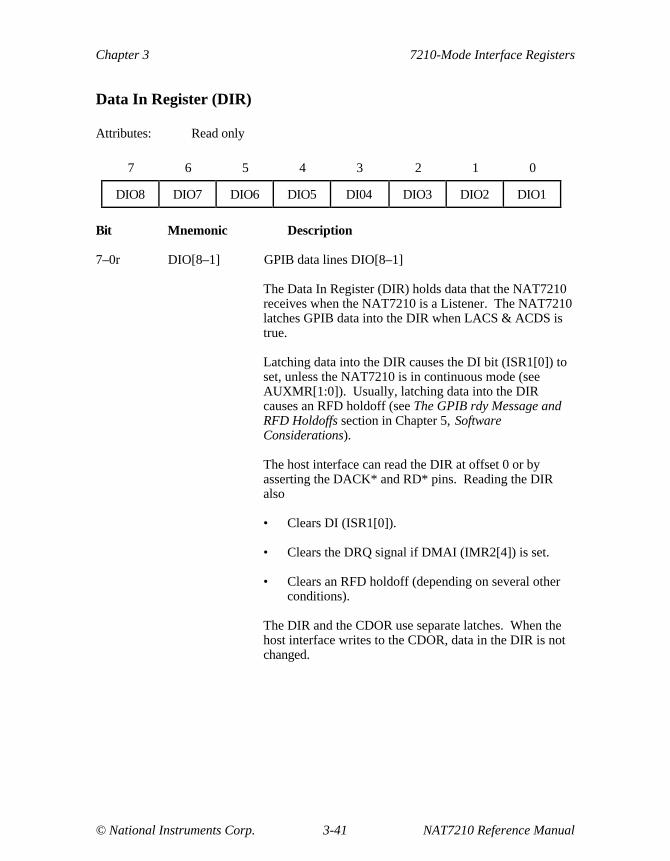
Chapter 3 7210-Mode Interface Registers
© National Instruments Corp. 3-41 NAT7210 Reference Manual
Data In Register (DIR)
Attributes: Read only
7 6 5 4 3 2 1 0
DIO8 DIO7 DIO6 DIO5 DI04 DIO3 DIO2 DIO1
Bit Mnemonic Description
7–0r DIO[8–1] GPIB data lines DIO[8–1]
The Data In Register (DIR) holds data that the NAT7210receives when the NAT7210 is a Listener. The NAT7210latches GPIB data into the DIR when LACS & ACDS istrue.
Latching data into the DIR causes the DI bit (ISR1[0]) toset, unless the NAT7210 is in continuous mode (seeAUXMR[1:0]). Usually, latching data into the DIRcauses an RFD holdoff (see The GPIB rdy Message andRFD Holdoffs section in Chapter 5, SoftwareConsiderations).
The host interface can read the DIR at offset 0 or byasserting the DACK* and RD* pins. Reading the DIRalso
• Clears DI (ISR1[0]).
• Clears the DRQ signal if DMAI (IMR2[4]) is set.
• Clears an RFD holdoff (depending on several otherconditions).
The DIR and the CDOR use separate latches. When thehost interface writes to the CDOR, data in the DIR is notchanged.
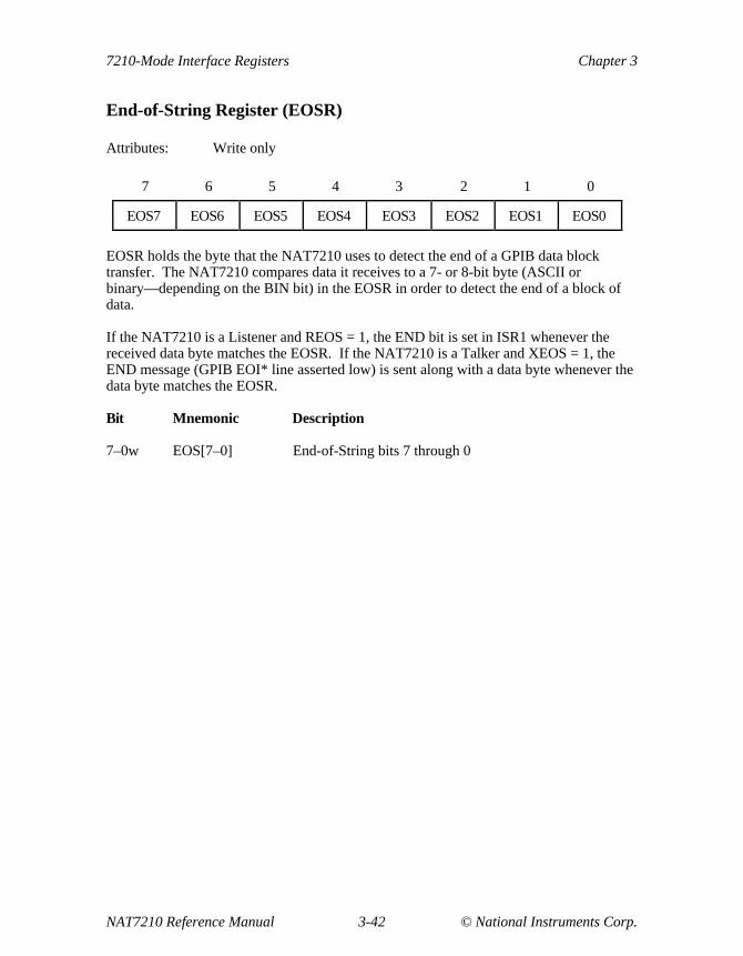
7210-Mode Interface Registers Chapter 3
NAT7210 Reference Manual 3-42 © National Instruments Corp.
End-of-String Register (EOSR)
Attributes: Write only
7 6 5 4 3 2 1 0
EOS7 EOS6 EOS5 EOS4 EOS3 EOS2 EOS1 EOS0
EOSR holds the byte that the NAT7210 uses to detect the end of a GPIB data blocktransfer. The NAT7210 compares data it receives to a 7- or 8-bit byte (ASCII orbinary—depending on the BIN bit) in the EOSR in order to detect the end of a block ofdata.
If the NAT7210 is a Listener and REOS = 1, the END bit is set in ISR1 whenever thereceived data byte matches the EOSR. If the NAT7210 is a Talker and XEOS = 1, theEND message (GPIB EOI* line asserted low) is sent along with a data byte whenever thedata byte matches the EOSR.
Bit Mnemonic Description
7–0w EOS[7–0] End-of-String bits 7 through 0

Chapter 3 7210-Mode Interface Registers
© National Instruments Corp. 3-43 NAT7210 Reference Manual
Internal Count Register (ICR)
Attributes: Write only
7 6 5 4 3 2 1 0
0 0 1 0 F3 F2 F1 F0
ICR determines the internal clock frequency of the NAT7210. You write to the ICR atthe same offset as the AUXMR.
Note: The ICR resets to 00101000 (8 MHz).
Bit Mnemonic Description
3–0 F(3–0) Clock Frequency
These bits, in addition to MICR (ICR2[0]), determine thelength of certain delays that are required by theIEEE 488 standard. You should set these bits accordingto the frequency of the signal driving the CLK pin. Forproper operation, set F(3–0) and MICR as follows:
ClockFrequency
MICR F(3–0)
1 0 0001
2 0 0010
3 0 0011
4 0 0100
5 0 0101
6 0 0110
7 0 0111
8 0 1000
10 1 0101
16 1 1000
20 1 1010
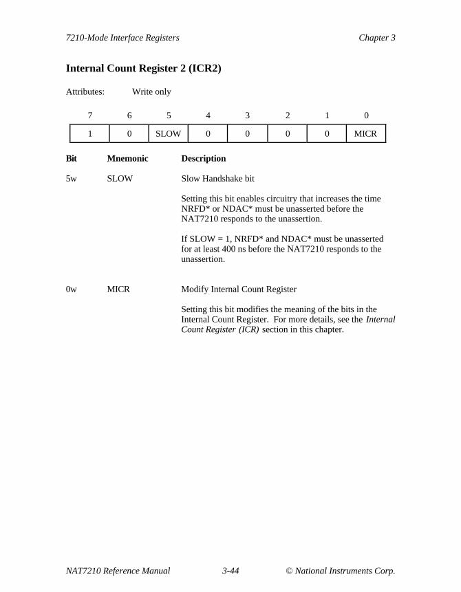
7210-Mode Interface Registers Chapter 3
NAT7210 Reference Manual 3-44 © National Instruments Corp.
Internal Count Register 2 (ICR2)
Attributes: Write only
7 6 5 4 3 2 1 0
1 0 SLOW 0 0 0 0 MICR
Bit Mnemonic Description
5w SLOW Slow Handshake bit
Setting this bit enables circuitry that increases the timeNRFD* or NDAC* must be unasserted before theNAT7210 responds to the unassertion.
If SLOW = 1, NRFD* and NDAC* must be unassertedfor at least 400 ns before the NAT7210 responds to theunassertion.
0w MICR Modify Internal Count Register
Setting this bit modifies the meaning of the bits in theInternal Count Register. For more details, see the InternalCount Register (ICR) section in this chapter.
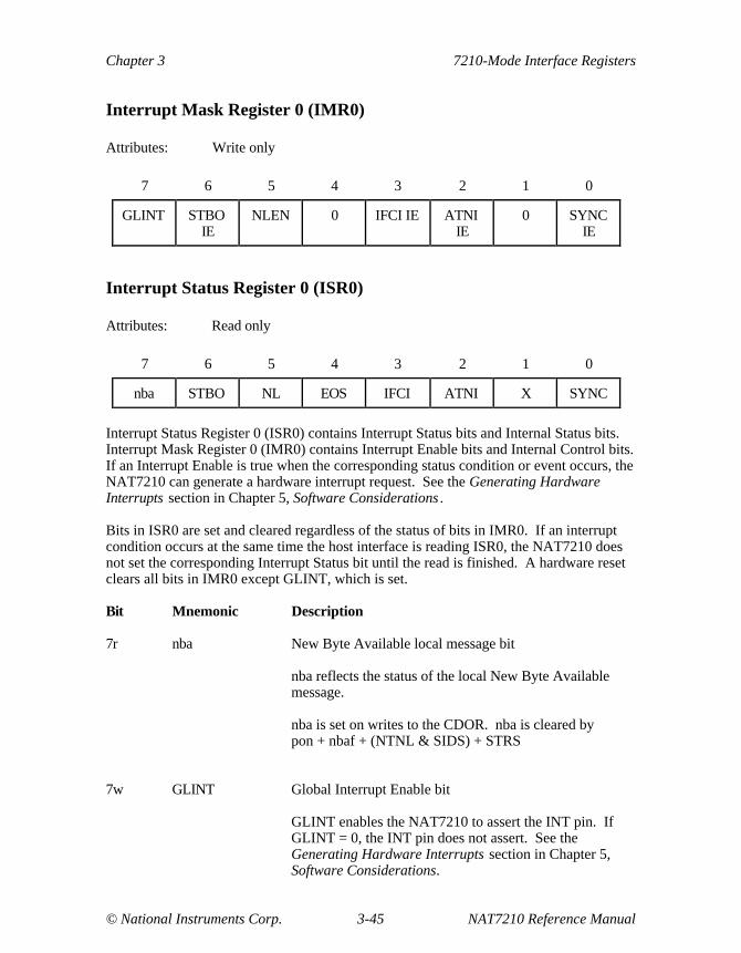
Chapter 3 7210-Mode Interface Registers
© National Instruments Corp. 3-45 NAT7210 Reference Manual
Interrupt Mask Register 0 (IMR0)
Attributes: Write only
7 6 5 4 3 2 1 0
GLINT STBOIE
NLEN 0 IFCI IE ATNIIE
0 SYNCIE
Interrupt Status Register 0 (ISR0)
Attributes: Read only
7 6 5 4 3 2 1 0
nba STBO NL EOS IFCI ATNI X SYNC
Interrupt Status Register 0 (ISR0) contains Interrupt Status bits and Internal Status bits.Interrupt Mask Register 0 (IMR0) contains Interrupt Enable bits and Internal Control bits.If an Interrupt Enable is true when the corresponding status condition or event occurs, theNAT7210 can generate a hardware interrupt request. See the Generating HardwareInterrupts section in Chapter 5, Software Considerations .
Bits in ISR0 are set and cleared regardless of the status of bits in IMR0. If an interruptcondition occurs at the same time the host interface is reading ISR0, the NAT7210 doesnot set the corresponding Interrupt Status bit until the read is finished. A hardware resetclears all bits in IMR0 except GLINT, which is set.
Bit Mnemonic Description
7r nba New Byte Available local message bit
nba reflects the status of the local New Byte Availablemessage.
nba is set on writes to the CDOR. nba is cleared bypon + nbaf + (NTNL & SIDS) + STRS
7w GLINT Global Interrupt Enable bit
GLINT enables the NAT7210 to assert the INT pin. IfGLINT = 0, the INT pin does not assert. See theGenerating Hardware Interrupts section in Chapter 5,Software Considerations.

7210-Mode Interface Registers Chapter 3
NAT7210 Reference Manual 3-46 © National Instruments Corp.
IMR0/ISR0 (continued)
Bit Mnemonic Description
6r STBO Status Byte Out bit6w STBO IE Status Byte Out Interrupt Enable bit
STBO IE determines how the NAT7210 requests serviceand responds to serial polls. See the Serial Pollingsection in Appendix B, Introduction to the GPIB.
If STBO IE = 0, the rsv bit in SPMR can be used torequest service. When the GPIB Controller serial pollsthe NAT7210, the NAT7210 transmits the current valueof SPMR.
If STBO IE = 1, the rsv bit in the SPMR has no effect onthe Service Request (SR1) function and rsv must begenerated through the reqt auxiliary command. STBOsets when the GPIB Controller serial polls the NAT7210.In response to STBO, the host interface writes a byte toSPMR, then the NAT7210 transmits this byte as the SerialPoll response.
STBO is set bySTBO IE & SPAS
STBO is cleared bypon + (write SPMR) + ~SPAS
5r NL New Line Receive bit
NL is set when the NAT7210 accepts the ASCII new linecharacter from the GPIB data bus.
NL is set byLACS & NL & ACDS
NL is cleared bypon + (LACS & ~NL & ACDS)

Chapter 3 7210-Mode Interface Registers
© National Instruments Corp. 3-47 NAT7210 Reference Manual
IMR0/ISR0 (continued)
Bit Mnemonic Description
5w NLEN New Line End Enable bit
If NLEN = 1, the NAT7210 treats the 7-bit ASCII newline character (0A hex) as an EOS character. TheAcceptor Handshake function responds to the acceptanceof a new line character in the same manner as if EOI weresent.
4r EOS End-of-String bit
The EOS bit indicates that the END bit in ISR1 was set bythe acceptance of the End-of-String character.
EOS is set byLACS & EOS & REOS & ACDS
EOS is cleared bypon + (LACS & ~EOS & ACDS) + ~REOS
3r IFCI IFC Interrupt bit3w IFCI IE IFC Interrupt Enable bit
IFCI is set on the assertion of the GPIB IFC* line.
IFCI is cleared bypon + (read ISR0) & ~SISB + clearIFCI
2r ATNI ATN Interrupt bit2w ATNI IE ATN Interrupt Enable bit
ATNI is set on the assertion of the ATN* line.
ATNI is cleared bypon + (read ISR0) & ~SISB + clearATNI
1r X Don’t care bit

7210-Mode Interface Registers Chapter 3
NAT7210 Reference Manual 3-48 © National Instruments Corp.
IMR0/ISR0 (continued)
Bit Mnemonic Description
0r SYNC GPIB Synchronization bit0w SYNC IE GPIB Synchronization Interrupt Enable bit
SYNC reflects the status of GPIB handshake lines after atransfer. SYNC is set at the completion of a transfer whenthe GPIB handshake is complete. An interrupt isgenerated when SYNC IE and SYNC are set.
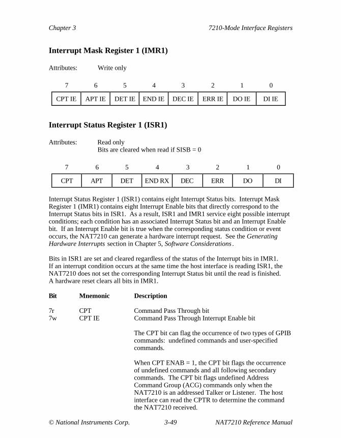
Chapter 3 7210-Mode Interface Registers
© National Instruments Corp. 3-49 NAT7210 Reference Manual
Interrupt Mask Register 1 (IMR1)
Attributes: Write only
7 6 5 4 3 2 1 0
CPT IE APT IE DET IE END IE DEC IE ERR IE DO IE DI IE
Interrupt Status Register 1 (ISR1)
Attributes: Read onlyBits are cleared when read if SISB = 0
7 6 5 4 3 2 1 0
CPT APT DET END RX DEC ERR DO DI
Interrupt Status Register 1 (ISR1) contains eight Interrupt Status bits. Interrupt MaskRegister 1 (IMR1) contains eight Interrupt Enable bits that directly correspond to theInterrupt Status bits in ISR1. As a result, ISR1 and IMR1 service eight possible interruptconditions; each condition has an associated Interrupt Status bit and an Interrupt Enablebit. If an Interrupt Enable bit is true when the corresponding status condition or eventoccurs, the NAT7210 can generate a hardware interrupt request. See the GeneratingHardware Interrupts section in Chapter 5, Software Considerations .
Bits in ISR1 are set and cleared regardless of the status of the Interrupt bits in IMR1.If an interrupt condition occurs at the same time the host interface is reading ISR1, theNAT7210 does not set the corresponding Interrupt Status bit until the read is finished.A hardware reset clears all bits in IMR1.
Bit Mnemonic Description
7r CPT Command Pass Through bit7w CPT IE Command Pass Through Interrupt Enable bit
The CPT bit can flag the occurrence of two types of GPIBcommands: undefined commands and user-specifiedcommands.
When CPT ENAB = 1, the CPT bit flags the occurrenceof undefined commands and all following secondarycommands. The CPT bit flags undefined AddressCommand Group (ACG) commands only when theNAT7210 is an addressed Talker or Listener. The hostinterface can read the CPTR to determine the commandthe NAT7210 received.
7210-Mode Interface Registers Chapter 3
NAT7210 Reference Manual 3-50 © National Instruments Corp.
IMR1/ISR1 (continued)
Bit Mnemonic Description
The CPT bit also flags the occurrence of commands thatyou specify when you set the AUXRE[3–0] orAUXRF[3–0] bits.
When the CPT bit flags a command, the NAT7210remains in a DAC Holdoff state until the host interfacewrites the valid or invalid auxiliary command to theAUXMR.
CPT is set by[UCG + ACG & (TADS + LADS)] & undefined& ACDS & CPT ENABLE+ UDPCF & SCG & ACDS & CPT ENABLE + DHADT & GET & ACDS+ DHADC & (SDC + DCL) & ACDS+ DHATA & TAG & ~UNT & ACDS+ DHALA & LAG & ~UNL & ACDS+ DHUNTL & (UNT + UNL) & ACDS+ DHALL & ATN & ACDS
CPT is cleared bypon + (read ISR1) & ~SISB + (read CPTR) &SISB
UDPCF is set by[UCG + ACG & (TADS + LADS)] & undefined& ACDS & CPT ENAB
UDPCF is cleared by[(UCG + ACG) & defined + TAG + LAG] &ACDS + ~(CPT ENAB) + pon
6r APT Address Pass Through bit6w APT IE Address Pass Through Interrupt Enable bit
APT indicates that the NAT7210 has received a secondaryGPIB address. The host interface can read the secondaryGPIB address in the CPTR.
Note: If the application program uses extended dualaddressing, it must check this bit.

Chapter 3 7210-Mode Interface Registers
© National Instruments Corp. 3-51 NAT7210 Reference Manual
IMR1/ISR1 (continued)
Bit Mnemonic Description
When APT sets, the NAT7210 enters the DAC Holdoffstate. When the host interface writes the valid or invalidauxiliary command to the AUXMR, the NAT7210 exitsthe DAC Holdoff state.
APT is set byADM1 & ADM0 & (TPAS + LPAS) & SCG &ACDS
APT is cleared bypon + (read ISR1) & ~SISB+ (valid + nonvalid) & SISB
5r DET Device Execute Trigger bit5w DET IE Device Execute Trigger Interrupt Enable bit
DET indicates that the NAT7210 received the GPIBGroup Execute Trigger (GET) command while theNAT7210 was a GPIB Listener.
DET is set byDTAS = GET & LADS & ACDS
DET is cleared bypon + (read ISR1) & ~SISB + clearDET
4r END RX End Received bit4w END IE End Received Interrupt Enable bit
END RX sets when the NAT7210, as a Listener, receivesa data byte satisfying the END condition. A data bytesatisfies the END condition if one of the followingconditions is true:
• REOS = 1 and the data byte matches the contents ofthe EOSR.
• NLEN = 1 and the data byte matches the ASCII newline character (hex 0A).
• The GPIB EOI signal is asserted when the byte isreceived.
7210-Mode Interface Registers Chapter 3
NAT7210 Reference Manual 3-52 © National Instruments Corp.
IMR1/ISR1 (continued)
Bit Mnemonic Description
END RX is set by(EOI + EOS & REOS + NL & NLEN) & ACDS& LACS
END RX is cleared bypon + (read ISR1) & ~SISB + clearEND
3r DEC Device Clear bit3w DEC IE Device Clear Interrupt Enable bit
DEC indicates that either the NAT7210 received theGPIB Device Clear (DCL) command or that theNAT7210 was a GPIB Listener and received the GPIBSelected Device Clear (SDC) command.
DEC is set byDCAS = (SDC & LADS + DCL) & ACDS
DEC is cleared bypon + (read ISR1) & ~SISB + clearDEC
2r ERR Error bit2w ERR IE Error Interrupt Enable bit
The definition of ERR depends on NTNL. WhenNTNL = 0, ERR indicates that the contents of the CDORhave been lost. ERR sets when the NAT7210 sends dataover the GPIB while no Listener exists on the GPIB.ERR also sets when a byte is written to the CDOR duringSIDS or when a transition from SDYS to SIDS occurs.
When NTNL = 1, ERR indicates that the sourcehandshake has attempted to send data or commands acrossthe bus but has found no Listeners (that is, NDAC andNRFD were unasserted). Data is not lost. The SHfunction does not source the data or command until aListener appears (that is, NDAC asserts).

Chapter 3 7210-Mode Interface Registers
© National Instruments Corp. 3-53 NAT7210 Reference Manual
IMR1/ISR1 (continued)
Bit Mnemonic Description
ERR is set by~NTNL & TACS & SDYS & DAC & RFD+ ~NTNL & SIDS & (write CDOR)+ ~NTNL & (SDYS to SIDS)+ NTNL & SDYS & EXTDAC & RFD
ERR is cleared bypon + (read ISR1) & ~SISB + clearERR
1r DO Data Out bit1w DO IE Data Out Interrupt Enable bit
DO indicates that the NAT7210, as GPIB Talker, is readyto accept another data byte into the CDOR. This data bytewill be transmitted to the GPIB. DO clears when a byte iswritten to the CDOR or when the NAT7210 ceases to bethe Active Talker.
DO is set byTACS & SGNS & ~nba
DO is cleared by~TACS + ~SGNS + nba + (read ISR1) & ~SISB
0r DI Data In bit0w DI IE Data In Interrupt Enable Bit
DI indicates that the NAT7210, as a GPIB Listener, hasaccepted a data byte from the GPIB Talker.
DI is set byLACS & ACDS & ~(continuous mode)
DI is cleared bypon + (read ISR1 & ~SISB) + (Finish Handshake& Holdoff mode) + (read DIR)

7210-Mode Interface Registers Chapter 3
NAT7210 Reference Manual 3-54 © National Instruments Corp.
Interrupt Mask Register 2 (IMR2)
Attributes: Write only
7 6 5 4 3 2 1 0
0 SRQI DMAO DMAI CO IE LOKCIE
REMCIE
ADSCIE
Interrupt Status Register 2 (ISR2)
Type: 7210 mode
Attributes: Read onlyBits clear when read if SISB = 0
7 6 5 4 3 2 1 0
INT SRQI LOK REM CO LOKC REMC ADSC
Interrupt Status Register 2 (ISR2) contains Interrupt Status bits and Internal Status bits.Interrupt Mask Register 2 (IMR2) contains Interrupt Enable bits and Internal Control bits.If an Interrupt Enable is true when the corresponding status condition or event occurs, theNAT7210 can generate a hardware interrupt request. See the Generating HardwareInterrupts section in Chapter 5, Software Considerations .
Bits in ISR2 are set and cleared regardless of the status of the bits in IMR2. If aninterrupt condition occurs at the same time the host interface is reading ISR2, theNAT7210 does not set the corresponding Interrupt Status bit until the read is finished.A hardware reset clears all bits in IMR2.
Bit Mnemonic Description
7r INT Interrupt bit
This bit is the logical OR of the Enabled Interrupt Statusbits in ISR0, ISR1, and ISR2.

Chapter 3 7210-Mode Interface Registers
© National Instruments Corp. 3-55 NAT7210 Reference Manual
IMR2/ISR2 (continued)
Bit Mnemonic Description
INT is set byGLINT & [(CPT & CPT IE) + (APT & APT IE)+ (DET & DET IE) + (ERR & ERR IE)+ (END RX & END IE) + (DEC & DEC IE)+ (DO & DO IE) + (DI & DI IE)+ (REMC & REMC IE) + (SRQI IE & SRQI)+ (LOKC & LOKC IE) + (CO IE & CO)+ (ADSC & ADSC IE) + (STBO IE & STBO)+ (IFCI IE & IFCI) + (ATNI IE & ATNI)+ (SYNC IE & SYNC)]
6r SRQI Service Request bit6w SRQI IE Service Request Interrupt Enable bit
SRQI indicates that the NAT7210, as CIC, received aGPIB Service Request (SRQ) message. SRQI is normallyedge sensitive; however, consider the following sequenceof events:
1. SRQ asserts, which asserts SRQI.
2. The control program clears SRQI, but SRQ remainsasserted.
3. The NAT7210 serial polls a device.
4. The device sends the RQS message to the NAT7210in response to the serial poll.
5. SRQ remains asserted because another device (notthe one being serial polled) is asserting SRQ.
In the situation outlined above, SRQI sets at the end of theserial poll, even if SRQ never unasserts. In addition, ifthe control program issues the clear SRQI auxiliarycommand while SRQ is asserted, the NAT7210 clearsSRQI for one clock pulse and then sets SRQI again.
SRQI is set by(CIC & SRQ & -(RQS & DAV)) becoming truewhere RQS = DIO7 & ~ATN & SPMS
SRQI is cleared bypon + (read ISR2) & ~SISB + clearSRQI
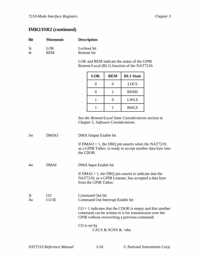
7210-Mode Interface Registers Chapter 3
NAT7210 Reference Manual 3-56 © National Instruments Corp.
IMR2/ISR2 (continued)
Bit Mnemonic Description
5r LOK Lockout bit4r REM Remote bit
LOK and REM indicate the status of the GPIBRemote/Local (RL1) function of the NAT7210.
LOK REM RL1 State
0 0 LOCS
0 1 REMS
1 0 LWLS
1 1 RWLS
See the Remote/Local State Considerations section inChapter 5, Software Considerations.
5w DMAO DMA Output Enable bit
If DMAO = 1, the DRQ pin asserts when the NAT7210,as a GPIB Talker, is ready to accept another data byte intothe CDOR.
4w DMAI DMA Input Enable bit
If DMAI = 1, the DRQ pin asserts to indicate that theNAT7210, as a GPIB Listener, has accepted a data bytefrom the GPIB Talker.
3r CO Command Out bit3w CO IE Command Out Interrupt Enable bit
CO = 1 indicates that the CDOR is empty and that anothercommand can be written to it for transmission over theGPIB without overwriting a previous command.
CO is set byCACS & SGNS & ~nba

Chapter 3 7210-Mode Interface Registers
© National Instruments Corp. 3-57 NAT7210 Reference Manual
IMR2/ISR2 (continued)
Bit Mnemonic Description
CO is cleared by(read ISR2) & ~SISB + ~CACS + ~SGNS +cdba
2r LOKC Lockout Change bit2w LOKC IE Lockout Change Interrupt Enable bit
LOKC sets when no change occurs in the LOK bit,ISR2[5]r.
LOKC is set byany change in LOK
LOKC is cleared bypon + (read ISR2) & ~SISB + clearLOKC
1r REMC Remote Change bit1w REMC IE Remote Change Interrupt Enable bit
REMC sets when no change occurs in the REM bit,ISR2[4]r.
REMC is set byany change in REM
REMC is cleared bypon + (read ISR2) & ~SISB + clearREMC
0r ADSC Addressed Status Change bit0w ADSC IE Addressed Status Change Interrupt Enable bit
ADSC sets when one of the following ADSR bitschanges: TA, LA, CIC, or MJMN.
ADSC is set by[(any change in TA) + (any change in LA)+ (any change in CIC) + (any change in MJMN)]& ~(lon + ton)
ADSC is cleared bypon + (read ISR2) & ~SISB + clearADSC + lon+ ton
7210-Mode Interface Registers Chapter 3
NAT7210 Reference Manual 3-58 © National Instruments Corp.
Parallel Poll Register (PPR)
Attributes: Write onlyAccessed at the same offset as AUXMR
7 6 5 4 3 2 1 0
0 1 1 U S P3 P2 P1
You use the Parallel Poll Register (PPR) to locally configure the manner in which theNAT7210 responds to a parallel poll. You write to the PPR at the same offset as theAUXMR. See the Parallel Polling section in Appendix B, Introduction to the GPIB .
When you use remote Parallel Poll Configuration (IEEE 488 capability code PP1), do notwrite to the PPR: writing to the PPR after it is remotely configured corrupts theconfiguration. The NAT7210 implements remote configuration fully and automaticallywithout software assistance. However, you must still set or clear the individual status(ist) message (by using Set/Clear Parallel Poll Flag auxiliary commands) according topre-established system protocol convention.
When you use the local Parallel Poll Configuration (capability code PP2), write to thePPR in advance of a poll. If PP2 (AUXRI[2]w) = 0, the contents written to the PPR areoverwritten if the Controller sends a Parallel Poll command (such as PPE or PPD while inPACS or PPU) that causes the remote configuration to override the local configuration.If PP2 = 1, the reception of parallel poll commands does not affect the contents of thePPR and the local configuration determines the response during parallel polls.
Bit Mnemonic Description
4w U Unconfigure bit
The U bit determines whether the NAT7210 is locallyconfigured to participate in parallel polls. If U = 1, theNAT7210 does not participate in parallel polls unless it isremotely configured to do so. If the host interface sets U,it should clear S and P[3–1] simultaneously.
If U = 0, the NAT7210 participates in parallel polls andresponds in the manner defined by PPR[3] throughPPR[0] and by ist. S and P[3–1] are the same as the bitsof the same name in the PPE message, and the I/O writeoperation to the PPR is the same as the receipt of the PPEmessage from the GPIB Controller.
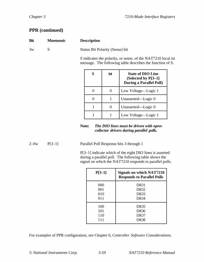
Chapter 3 7210-Mode Interface Registers
© National Instruments Corp. 3-59 NAT7210 Reference Manual
PPR (continued)
Bit Mnemonic Description
3w S Status Bit Polarity (Sense) bit
S indicates the polarity, or sense, of the NAT7210 local istmessage. The following table describes the function of S.
S ist State of DIO Line(Selected by P[3–1]
During a Parallel Poll)
0 0 Low Voltage—Logic 1
0 1 Unasserted—Logic 0
1 0 Unasserted—Logic 0
1 1 Low Voltage—Logic 1
Note: The DIO lines must be driven with open-collector drivers during parallel polls.
2–0w P[3–1] Parallel Poll Response bits 3 through 1
P[3–1] indicate which of the eight DIO lines is assertedduring a parallel poll. The following table shows thesignal on which the NAT7210 responds to parallel polls.
P[3–1] Signals on which NAT7210Responds to Parallel Polls
000001010011
DIO1DIO2DIO3DIO4
100101110111
DIO5DIO6DIO7DIO8
For examples of PPR configuration, see Chapter 6, Controller Software Considerations.

7210-Mode Interface Registers Chapter 3
NAT7210 Reference Manual 3-60 © National Instruments Corp.
Source/Acceptor Status Register (SASR)
Attributes: Read only
7 6 5 4 3 2 1 0
nba AEHS ANHS1 ANHS2 ADHS ACRDY SH1A SH1B
The Source/Acceptor Status Register (SASR) contains status bits that you can use todetermine the state of the Source and Acceptor functions.
Bit Mnemonic Description
7r nba New Byte Available local message
6r AEHS Acceptor End Holdoff State bit
5r ANHS1 Acceptor Not Ready Holdoff bit
4r ANHS2 Acceptor Not Ready Holdoff Immediately bit
3r ADHS Acceptor Data Holdoff State bit
2r ACRDY Acceptor Ready State bit
Use this bit to determine the state of the AcceptorHandshake. By monitoring the LA and ATN bits in theADSR, the DAV bit in the BSR, and the ADHS andACRDY bits, you can determine the state of the AcceptorHandshake function as described below:
AIDS = ~ATN & ~LAANRS = ~AIDS & ~ACRDY & ~DAVACRS = ~AIDS & ACRDY & ~DAVACDS = ~AIDS & ACRDY & DAV
+ ~AIDS & ~ACRDY & DAV & ATN & ADHS
AWNS = ~AIDS & ~ACRDY & DAV & ~(ATN & ADHS)

Chapter 3 7210-Mode Interface Registers
© National Instruments Corp. 3-61 NAT7210 Reference Manual
SASR (continued)
Bit Mnemonic Description
1–0r SH1A, SH1B Source Handshake State bits
Use these bits to determine the state of the SourceHandshake interface function. By monitoring the TA,Serial Poll Mode State (SPMS), ATN bits in the ADSR,and the SH1A and SH1B bits, you can determine the stateof the Source Handshake function as described below:
SIDS = ~(TACS & ~ATN + CIC & ATN)SGNS = ~SIDS & ~SH1A & ~SH1BSDYS = ~SIDS & SH1ASTRS = ~SIDS & ~SH1A & SH1B

7210-Mode Interface Registers Chapter 3
NAT7210 Reference Manual 3-62 © National Instruments Corp.
Serial Poll Mode Register (SPMR)
Attributes: Write only
7 6 5 4 3 2 1 0
S8 rsv/RQS S6 S5 S4 S3 S2 S1
Serial Poll Status Register (SPSR)
Attributes: Read only
7 6 5 4 3 2 1 0
S8 PEND S6 S5 S4 S3 S2 S1
Bit Mnemonic Description
7r, S8 Serial Poll Status bit 87w
5–0r, S[6–1] Serial Poll Status bits 6 through 15–0w
These bits send device- or system-dependent statusinformation over the GPIB when the Controller serialpolls the NAT7210.
When STBO IE = 0, the NAT7210 transmits a byte ofstatus information, SPMR[7–0], to the CIC if the CICserial polls the NAT7210. The SPMR bits S[8, 6–1] aredouble buffered. If the host interface writes to the SPMRduring a serial poll when SPAS is active, the NAT7210saves the value. The NAT7210 updates the SPMR whenthe NAT7210 exits SPAS.
When STBO IE = 1 and the Controller serial polls theNAT7210, the STBO interrupt condition sets. The hostinterface should write the STB and the RQS bit to theSPMR in response to an STBO interrupt.
Issuing the Chip Reset auxiliary command clears thesebits.
Chapter 3 7210-Mode Interface Registers
© National Instruments Corp. 3-63 NAT7210 Reference Manual
SPMR/SPSR (continued)
Bit Mnemonic Description
6r PEND Pending bit
PEND sets when rsv = 1. PEND clears when theNAT7210 is in the Negative Poll Response State (NPRS)and the local Request Service (rsv) message is false. Byreading the PEND status bit, you can confirm that arequest was accepted and that the Status Byte (STB) wastransmitted (PEND = 0).
6w rsv/RQS Request Service/ RQS bit
When STBO IE = 0, bit 6 is the rsv bit. The rsv bitgenerates the GPIB local rsv message. When rsv = 1 andthe GPIB Controller is not serial polling the NAT7210,the NAT7210 enters the Service Request State (SRQS)and asserts the GPIB SRQ signal. When the Controllerreads the STB during the poll, the NAT7210 clears rsv.The rsv bit is also cleared by a hardware reset or bywriting 0 to it. Issuing the Chip Reset auxiliary commandalso clears rsv.
When STBO IE = 1, bit 6 is the RQS bit. When theController serial polls the NAT7210, the STBO interruptcondition sets. The host interface should write the STBand the RQS bit to the SPMR in response to an STBOinterrupt. The NAT7210 transfers the STB and RQS tothe Controller during that particular serial poll. Ahardware reset clears RQS. Issuing the Chip Resetauxiliary command also clears RQS.
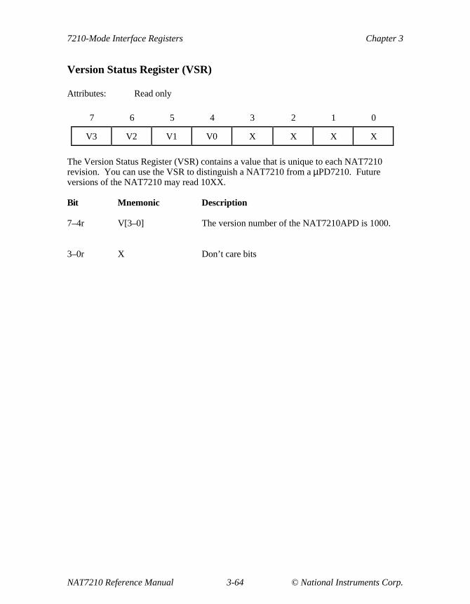
7210-Mode Interface Registers Chapter 3
NAT7210 Reference Manual 3-64 © National Instruments Corp.
Version Status Register (VSR)
Attributes: Read only
7 6 5 4 3 2 1 0
V3 V2 V1 V0 X X X X
The Version Status Register (VSR) contains a value that is unique to each NAT7210revision. You can use the VSR to distinguish a NAT7210 from a µPD7210. Futureversions of the NAT7210 may read 10XX.
Bit Mnemonic Description
7–4r V[3–0] The version number of the NAT7210APD is 1000.
3–0r X Don’t care bits

© National Instruments Corp. 4-1 NAT7210 Reference Manual
Chapter 49914-Mode Interface Registers
This chapter contains NAT7210 address maps and detailed descriptions of the NAT7210interface registers in 9914 mode. For 7210-mode register descriptions, see Chapter 3,7210-Mode Interface Registers.
9914 Register Map
Table 4-1 is the register bit map for the NAT7210 in 9914 mode.
Notice that bold-ruled cells distinguish six registers that are accessible only when thePage-In state is true. Refer to The Page-In Condition section that immediately followsthe register map for more information.

9914-Mode Interface Registers Chapter 49914 Mode Only
NAT7210 Reference Manual 4-2 © National Instruments Corp.
Table 4-1. 9914-Mode Interface Registers
Key
= 9914-Mode Paged Registers= Read Register= Write Register
RW
7 6 5 4 3 2 1 0
ISR0 +0 INT0 INT1 BI BO END SPAS RLC MAC R
IMR0 +0 DMAO DMAI BI IE BO IE END IE SPAS IE RLC IE MAC IE W
ISR1 +1 GET ERR UNC APT DCAS MA SRQ IFC R
IMR1 +1 GET IE ERR IE UNC IE APT IE DCAS IE MA IE SRQ IE IFC IE W
ADSR +2 REM LLO ATN LPAS TPAS LA TA ulpa R
IMR2 +2 GLINT STBO IE NLEN 0 LLOC IE ATNI IE 0 CIC IE W
EOSR +2 EOS7 EOS6 EOS5 EOS4 EOS3 EOS2 EOS1 EOS0 W
BCR +2 ATN DAV NDAC NRFD EOI SRQ IFC REN W
ACCR +2 ACC7 ACC6 ACC5 ACC4 ACC3 ACC2 ACC1 ACC0 W
BSR +3 ATN DAV NDAC NRFD EOI SRQ IFC REN R
AUXCR +3 C/S 0 0 F4 F3 F2 F1 F0 W
ISR2 +4 nba STBO NL EOS LLOC ATNI X CIC R
ADR +4 edpa dal dat A5 A4 A3 A2 A1 W
SPSR +5 S8 PEND S6 S5 S4 S3 S2 S1 R
SPMR +5 S8 rsv/RQS S6 S5 S4 S3 S2 S1 W
CPTR +6 CPT7 CPT6 CPT5 CPT4 CPT3 CPT2 CPT1 CPT0 R
PPR +6 PP8 PP7 PP6 PP5 PP4 PP3 PP2 PP1 W
DIR +7 DIO8 DIO7 DIO6 DIO5 DIO4 DIO3 DIO2 DIO1 R
CDOR +7 DIO8 DIO7 DIO6 DIO5 DIO4 DIO3 DIO2 DIO1 W

Chapter 4 9914-Mode Interface Registers9914 Mode Only
© National Instruments Corp. 4-3 NAT7210 Reference Manual
The Page-In Condition
Four writable registers can appear at the same offset as the Address Status Register(ADSR) (offset 4). After a hardware or software reset, no writable register appears at theADSR offset: the NAT7210 ignores writes to that offset.
One Page-In auxiliary command exists for each of the four registers. The host interfacecan make one of the four registers accessible by issuing the appropriate Page-Incommand to the Auxiliary Command Register (AUXCR). The paged-in register remainsaccessible at the ADSR offset until the host interface pages-in another register or issuesthe Clear Page-In Register auxiliary command.
When any one of the four writable registers is accessible at the ADSR offset, InterruptStatus Register 2 (ISR2) is accessible at the same offset as ADR, and the Serial PollStatus Register (SPSR) is accessible at the same offset as the Serial Poll Mode Register(SPMR).
Hidden Registers
In addition to the registers shown in Table 4-1, the NAT7210 contains hidden registers.All hidden registers are write-only registers. Two or more hidden registers can appear atthe same offset. When you write an 8-bit pattern to these offsets, some of the bitsdetermine which hidden register will be written. The other bits represent the valuewritten to the register.
Accessory Read Register Map
Several hidden registers appear at the ACCR offset. Table 4-2 shows these hiddenregisters.
Table 4-2. Hidden Registers at the ACCR Offset
Register Bit 7 Bit 6 Bit 5 Bit 4 Bit 3 Bit 2 Bit 1 Bit 0
ICR 0 0 1 0 F3 F2 F1 F0
ACCA 1 0 0 BIN XEOS REOS 0 0
ACCB 1 0 1 ISS INV LWC SPEOI ATCT
ACCE 1 1 0 0 DHADT DHADC 0 0
ACCF 1 1 0 1 DHATA DHALA DHUNTL DHALL
ACCI 1 1 1 0 USTD PP1 0 DMAE

9914-Mode Interface Registers Chapter 49914 Mode Only
NAT7210 Reference Manual 4-4 © National Instruments Corp.
Register Bit Descriptions
Some 7210-mode registers and 9914-mode registers share identical names. The7210-mode registers are described in Chapter 3, 7210-Mode Interface Registers. If youare using the NAT7210 in 9914 mode, be sure to read the proper description for the9914-mode registers.
All registers are listed in alphabetical order. The registers are alphabetized according totheir mnemonics.

Chapter 4 9914-Mode Interface Registers9914 Mode Only
© National Instruments Corp. 4-5 NAT7210 Reference Manual
Accessory Register A (ACCRA)
Attributes: Write onlyAccessed at the same offset as ACCR
7 6 5 4 3 2 1 0
1 0 0 BIN XEOS REOS 0 0
Accessory Register A (ACCRA) controls the EOS and END messages. A hardware resetor the ch_rst auxiliary command clears ACCRA.
Bit Mnemonic Description
4w BIN Binary bit
The BIN bit selects the length of the EOS message. IfBIN = 1, the EOSR is treated as an 8-bit byte. WhenBIN = 0, the EOSR is treated as a 7-bit register (forASCII characters), and only a 7-bit comparison is donewith the data on the GPIB.
3w XEOS Transmit END With EOS bit
The XEOS bit permits or prohibits automatic transmissionof the GPIB END message at the same time as the EOSmessage when the NAT7210 is in Talker Active State(TACS). If XEOS = 1 and the byte in the CDOR matchesthe contents of the EOSR, the EOI line is sent true alongwith the data.
2w REOS END On EOS Received bit
The REOS bit permits or prohibits setting the END bit(ISR0[3]r) when the NAT7210 receives the EOS messageas a Listener. If REOS = 1 and the byte in the DIRmatches the byte in the EOSR, the END bit (ISR1[4]r) isset and the acceptor function treats the EOS character justas if it were received with EOI asserted.

9914-Mode Interface Registers Chapter 49914 Mode Only
NAT7210 Reference Manual 4-6 © National Instruments Corp.
Accessory Register B (ACCRB)
Attributes: Write onlyAccessed at the same offset as ACCR
7 6 5 4 3 2 1 0
1 0 1 ISS INV LWC SPEOI ATCT
Bit Mnemonic Description
4w ISS Individual Status Select bit
ISS determines the value of the NAT7210 ist message.When ISS = 1, ist takes on the value of the NAT7210SRQS. (The NAT7210 is asserting the GPIB SRQmessage when it is in SRQS.) If ISS = 0, ist takes on thevalue of the NAT7210 Parallel Poll Flag. You set andclear the Parallel Poll Flag by using the Set Parallel PollFlag and Clear Parallel Poll Flag auxiliary commands.
3w INV Invert bit
INV determines the polarity of the INT pin.
INV Bit INT Pin Polarity
0 Active High
1 Active Low
See the Generating Hardware Interrupts section inChapter 5, Software Considerations.
2w LWC Listen When Controller bit
LWC enables the NAT7210 to accept command bytes thatthe NAT7210 sources when it is CIC. If LWC = 0, theNAT7210 does not accept command bytes sent by theNAT7210.

Chapter 4 9914-Mode Interface Registers9914 Mode Only
© National Instruments Corp. 4-7 NAT7210 Reference Manual
ACCRB (continued)
Bit Mnemonic Description
1w SPEOI Send Serial Poll EOI bit
SPEOI determines whether the NAT7210 sends EOIwhen a Controller serial polls the NAT7210.
SPEOI EOI During Serial Polls
0 Sent False
1 Sent True
0w ATCT Automatic Take Control bit
If ATCT = 1, the NAT7210 can—without softwareintervention—take control when another CIC passescontrol to the NAT7210. Use the CIC bit (ISR2[0] todetermine when the NAT7210 receives control. See theGPIB Controller Considerations section in Chapter 6,Controller Software Considerations.
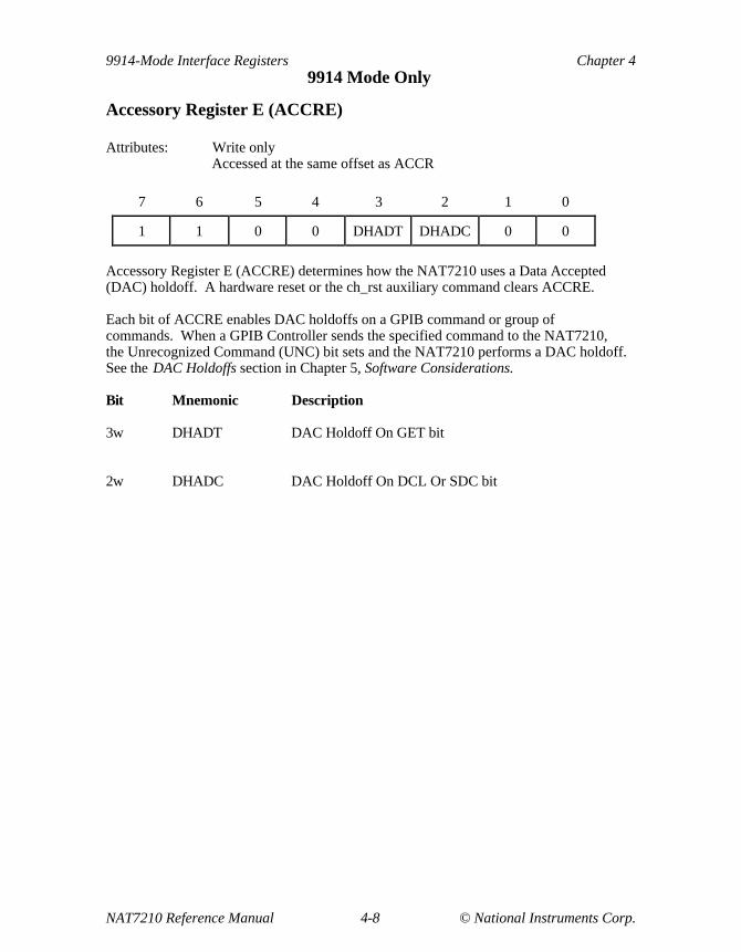
9914-Mode Interface Registers Chapter 49914 Mode Only
NAT7210 Reference Manual 4-8 © National Instruments Corp.
Accessory Register E (ACCRE)
Attributes: Write onlyAccessed at the same offset as ACCR
7 6 5 4 3 2 1 0
1 1 0 0 DHADT DHADC 0 0
Accessory Register E (ACCRE) determines how the NAT7210 uses a Data Accepted(DAC) holdoff. A hardware reset or the ch_rst auxiliary command clears ACCRE.
Each bit of ACCRE enables DAC holdoffs on a GPIB command or group ofcommands. When a GPIB Controller sends the specified command to the NAT7210,the Unrecognized Command (UNC) bit sets and the NAT7210 performs a DAC holdoff.See the DAC Holdoffs section in Chapter 5, Software Considerations.
Bit Mnemonic Description
3w DHADT DAC Holdoff On GET bit
2w DHADC DAC Holdoff On DCL Or SDC bit

Chapter 4 9914-Mode Interface Registers9914 Mode Only
© National Instruments Corp. 4-9 NAT7210 Reference Manual
Accessory Register F (ACCRF)
Attributes: Write onlyAccessed at the same offset as ACCR
7 6 5 4 3 2 1 0
1 1 0 1 DHATA DHALA DHUNTL DHALL
Accessory Register F (ACCRF) determines how the NAT7210 uses a DAC holdoff.A hardware reset or the ch_rst auxiliary command clears ACCRF.
Each bit of ACCRF enables DAC holdoffs on a GPIB command or group of commands.When a GPIB Controller sends the specified command to the NAT7210, the UNC bit setsand the NAT7210 performs a DAC holdoff. See the DAC Holdoffs section in Chapter 5,Software Considerations.
Bit Mnemonic Description
3w DHATA DAC Holdoff On All Talker Addresses bit
2w DHALA DAC Holdoff On All Listener Addresses bit
1w DHUNTL DAC Holdoff On The UNT Or UNL Command bit
0w DHALL DAC Holdoff On All UCG, ACG, And SCG Commandsbit

9914-Mode Interface Registers Chapter 49914 Mode Only
NAT7210 Reference Manual 4-10 © National Instruments Corp.
Accessory Register I (ACCRI)
Attributes: Write onlyAccessed at the same offset as ACCR
7 6 5 4 3 2 1 0
1 1 1 0 USTD PP1 0 DMAE
Bit Mnemonic Description
3w USTD Ultra Short T1 Delay bit
If USTD = 1, the T1 delay can be as short as 350 ns. Seethe T1 Delay Generation section in Chapter 5, SoftwareConsiderations.
2w PP1 Parallel Poll bit 1
The PP1 bit permits or prohibits the NAT7210’s abilityto automatically respond to remote parallel pollconfiguration. If PP1 = 1, the NAT7210 can beconfigured remotely for parallel polls without softwareintervention.
The Acceptor Handshake does not perform a DACholdoff or set the UNC bit when it receives a Parallel PollCommand (PPC or PPU).
If PP1 = 0, parallel polls must be configured through thePPR, and Parallel Poll commands must be monitored byUNC.
0w DMAE DMA Enable bit
DMAE lets you use DMAO (IMR0[7]) and DMAI(IMR0[6]) to enable the DRQ signal.
If DMAE = 0, DRQ always asserts when the NAT7210receives a data byte as a Listener or when the NAT7210 isa Talker and the CDOR is empty.
DRQ is cleared bypon + (read DIR) + (write CDOR)

Chapter 4 9914-Mode Interface Registers9914 Mode Only
© National Instruments Corp. 4-11 NAT7210 Reference Manual
Address Register (ADR)
Attributes: Write only
7 6 5 4 3 2 1 0
edpa dal dat A5 A4 A3 A2 A1
ADR is used to load the primary GPIB address of the interface.
Bit Mnemonic Description
7w edpa Enable Dual Primary Addressing Mode bit
Setting edpa enables the dual primary addressing mode ofthe NAT7210. If edpa = 1, the NAT7210 ignores the leastsignificant bit (A1) of its GPIB address. The NAT7210then has two consecutive primary addresses. The ulpa bitin the Address Status Register indicates which address isactive.
6w dal Disable Listener bit
Setting dal returns the NAT7210 Listener function toLIDS and forces the NAT7210 Listener function toremain in LIDS even if the chip receives its GPIB listenaddress or a lon auxiliary command.
5w dat Disable Talker bit
Setting dat returns the NAT7210 Talker function to TIDSand forces the Talker function to remain in TIDS even ifthe chip receives its GPIB talk address or a ton auxiliarycommand.
4–0w A[5–1] NAT7210 GPIB Address bits 5 through 1
A[5–1] specify the primary GPIB address of theNAT7210. The corresponding GPIB talk address isformed by adding hex 40 to A[5–1], while thecorresponding GPIB listen address is formed by addinghex 20. A[5–1] should not be 11111 (binary) to preventthe corresponding talk and listen addresses fromconflicting with the GPIB UNT and GPIB UNLcommands.
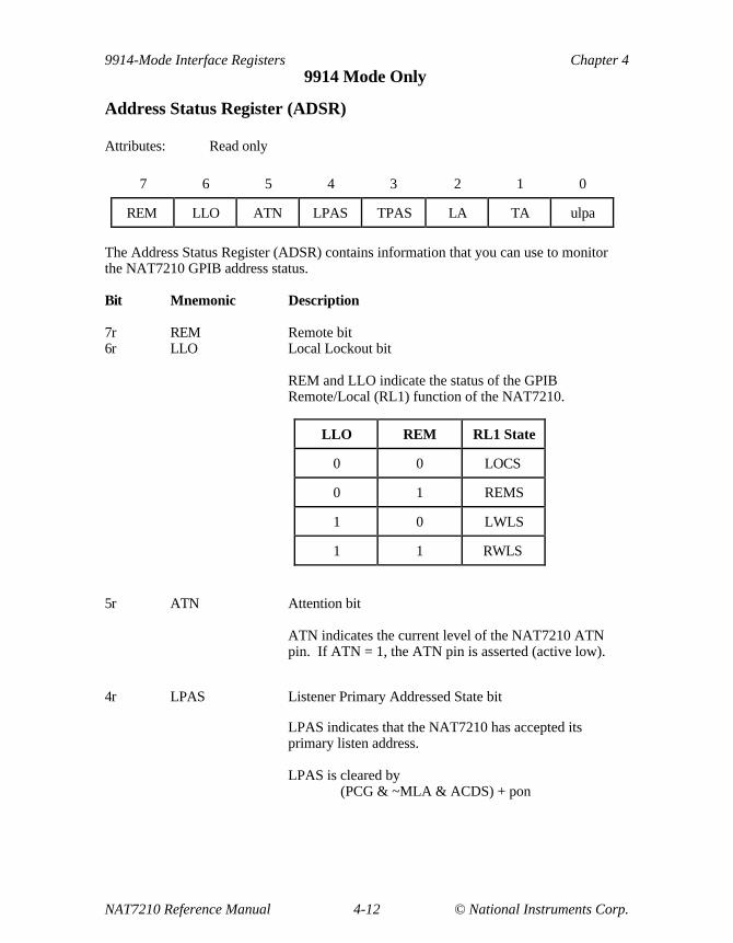
9914-Mode Interface Registers Chapter 49914 Mode Only
NAT7210 Reference Manual 4-12 © National Instruments Corp.
Address Status Register (ADSR)
Attributes: Read only
7 6 5 4 3 2 1 0
REM LLO ATN LPAS TPAS LA TA ulpa
The Address Status Register (ADSR) contains information that you can use to monitorthe NAT7210 GPIB address status.
Bit Mnemonic Description
7r REM Remote bit6r LLO Local Lockout bit
REM and LLO indicate the status of the GPIBRemote/Local (RL1) function of the NAT7210.
LLO REM RL1 State
0 0 LOCS
0 1 REMS
1 0 LWLS
1 1 RWLS
5r ATN Attention bit
ATN indicates the current level of the NAT7210 ATNpin. If ATN = 1, the ATN pin is asserted (active low).
4r LPAS Listener Primary Addressed State bit
LPAS indicates that the NAT7210 has accepted itsprimary listen address.
LPAS is cleared by(PCG & ~MLA & ACDS) + pon
Chapter 4 9914-Mode Interface Registers9914 Mode Only
© National Instruments Corp. 4-13 NAT7210 Reference Manual
ADSR (continued)
Bit Mnemonic Description
3r TPAS Talker Primary Addressed State bit
TPAS indicates that the NAT7210 has accepted itsprimary talk address.
TPAS is cleared by(PCG & ~MTA & ACDS) + pon
2r LA Listener Active bit
LA = 1 when the NAT7210 has been addressed orprogrammed as a GPIB Listener—that is, the NAT7210 isin LACS or LADS. The NAT7210 is addressed to listenwhen it receives its listen address from the CIC. You canalso program the NAT7210 to listen by using theListen-Only auxiliary command.
If the NAT7210 is addressed to listen, it is automaticallyunaddressed to talk.
LA is cleared bypon + IFC + (UNL & ACDS)
1r TA Talker Active bit
TA = 1 when the NAT7210 has been addressed orprogrammed as the GPIB Talker—that is, the NAT7210 isin TACS, TADS, or SPAS. The NAT7210 can beaddressed to talk when it receives its talk address from theCIC. You can also program the NAT7210 to talk byusing the Talk-Only auxiliary command.
If the NAT7210 is addressed to talk, it is automaticallyunaddressed to listen.
TA is cleared bypon + IFC + (OTA & ACDS)

9914-Mode Interface Registers Chapter 49914 Mode Only
NAT7210 Reference Manual 4-14 © National Instruments Corp.
ADSR (continued)
Bit Mnemonic Description
0r ulpa Upper/Lower Primary Address bit
ulpa indicates the least significant bit of the last primaryaddress that the NAT7210 received.
Note: Only one Talker or Listener is active at a time.ulpa indicates which, if either, NAT7210 Talkeror Listener function is addressed or active.
The ch_rst auxiliary command clears the ulpa bit in theADSR.
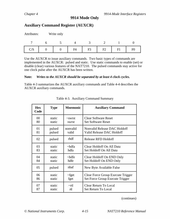
Chapter 4 9914-Mode Interface Registers9914 Mode Only
© National Instruments Corp. 4-15 NAT7210 Reference Manual
Auxiliary Command Register (AUXCR)
Attributes: Write only
7 6 5 4 3 2 1 0
C/S 0 0 F4 F3 F2 F1 F0
Use the AUXCR to issue auxiliary commands. Two basic types of commands areimplemented in the AUXCR: pulsed and static. Use static commands to enable (set) ordisable (clear) various features of the NAT7210. The pulsed commands stay active forone clock pulse after the AUXCR has been written.
Note: Writes to the AUXCR should be separated by at least 4 clock cycles.
Table 4-3 summarizes the AUXCR auxiliary commands and Table 4-4 describes theAUXCR auxiliary commands.
Table 4-3. Auxiliary Command Summary
HexCode
Type Mnemonic Auxiliary Command
0080
staticstatic
~swrstswrst
Clear Software ResetSet Software Reset
0181
pulsedpulsed
nonvalidvalid
Nonvalid Release DAC HoldoffValid Release DAC Holdoff
02 pulsed rhdf Release RFD Holdoff
0383
staticstatic
~hdfahdfa
Clear Holdoff On All DataSet Holdoff On All Data
0484
staticstatic
~hdfehdfe
Clear Holdoff On END OnlySet Holdoff On END Only
05 pulsed nbaf New Byte Available False
0686
staticstatic
~fgetfget
Clear Force Group Execute TriggerSet Force Group Execute Trigger
0787
staticstatic
~rtlrtl
Clear Return To LocalSet Return To Local
(continues)
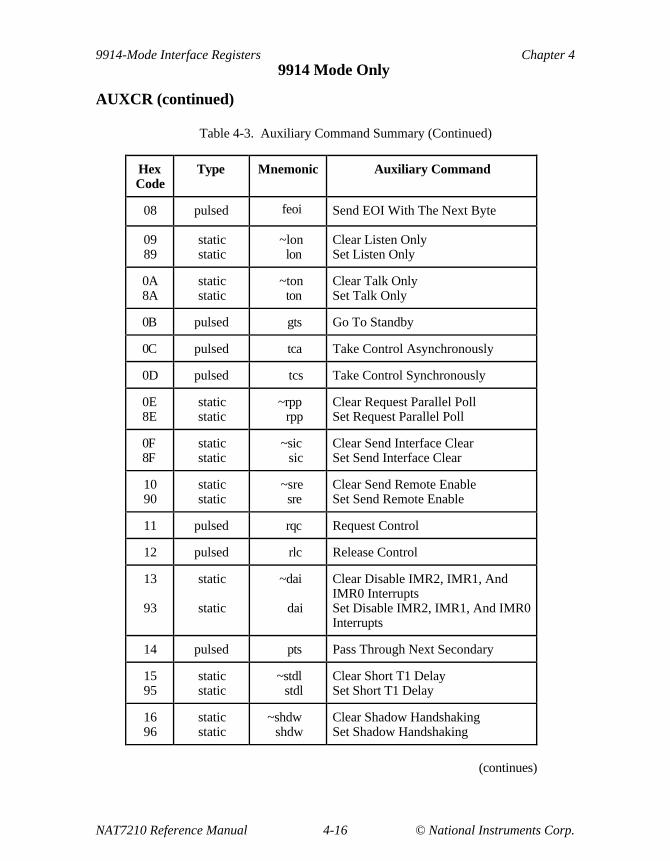
9914-Mode Interface Registers Chapter 49914 Mode Only
NAT7210 Reference Manual 4-16 © National Instruments Corp.
AUXCR (continued)
Table 4-3. Auxiliary Command Summary (Continued)
HexCode
Type Mnemonic Auxiliary Command
08 pulsed feoi Send EOI With The Next Byte
0989
staticstatic
~lonlon
Clear Listen OnlySet Listen Only
0A8A
staticstatic
~tonton
Clear Talk OnlySet Talk Only
0B pulsed gts Go To Standby
0C pulsed tca Take Control Asynchronously
0D pulsed tcs Take Control Synchronously
0E8E
staticstatic
~rpprpp
Clear Request Parallel PollSet Request Parallel Poll
0F8F
staticstatic
~sicsic
Clear Send Interface ClearSet Send Interface Clear
1090
staticstatic
~sresre
Clear Send Remote EnableSet Send Remote Enable
11 pulsed rqc Request Control
12 pulsed rlc Release Control
13
93
static
static
~dai
dai
Clear Disable IMR2, IMR1, AndIMR0 InterruptsSet Disable IMR2, IMR1, And IMR0Interrupts
14 pulsed pts Pass Through Next Secondary
1595
staticstatic
~stdlstdl
Clear Short T1 DelaySet Short T1 Delay
1696
staticstatic
~shdwshdw
Clear Shadow HandshakingSet Shadow Handshaking
(continues)

Chapter 4 9914-Mode Interface Registers9914 Mode Only
© National Instruments Corp. 4-17 NAT7210 Reference Manual
AUXCR (continued)
Table 4-3. Auxiliary Command Summary (Continued)
HexCode
Type Mnemonic Auxiliary Command
1797
staticstatic
~vstdlvstdl
Clear Very Short T1 DelaySet Very Short T1 Delay
1898
staticstatic
~rsv2rsv2
Clear Request Service bit 2Set Request Service bit 2
99 pulsed sw7210 Switch To 7210 Mode
1A9A
pulsedpulsed
reqfreqt
Request rsv False (reqf)Request rsv True (reqt)
1C pulsed ch_rst Chip Reset
1D9D
staticstatic
~istist
Clear Parallel Poll FlagSet Parallel Poll Flag
1E pulsed piimr2 Page-In Interrupt Mask Register 2
1F pulsed pibcr Page-In Bus Control Register
9C pulsed clrpi Clear Page-In Registers
9E pulsed pieosr Page-In End-of-String Register
9F pulsed piaccr Page-In Accessory Register
Values not specified are reserved.
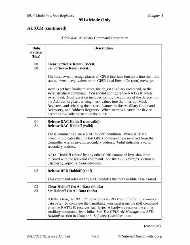
9914-Mode Interface Registers Chapter 49914 Mode Only
NAT7210 Reference Manual 4-18 © National Instruments Corp.
AUXCR (continued)
Table 4-4. Auxiliary Command Description
DataPattern(Hex)
Description
0080
Clear Software Reset (~swrst)Set Software Reset (swrst)
The local swrst message places all GPIB interface functions into their idlestates. swrst is equivalent to the GPIB local Power On (pon) message.
swrst is set by a hardware reset, the ch_rst auxiliary command, or theswrst auxiliary command. You should configure the NAT7210 whileswrst is set. Configuration includes writing the address of the device intothe Address Register, writing mask values into the Interrupt MaskRegisters, and selecting the desired features in the Auxiliary Command,Accessory, and Address Registers. When swrst is cleared, the devicebecomes logically existent on the GPIB.
0181
Release DAC Holdoff (nonvalid)Release DAC Holdoff (valid)
These commands clear a DAC holdoff condition. When APT = 1,nonvalid indicates that the last GPIB command byte received from theController was an invalid secondary address. Valid indicates a validsecondary address.
A DAC holdoff caused by any other GPIB command byte should bereleased with the nonvalid command. See the DAC Holdoffs section inChapter 5, Software Considerations.
02 Release RFD Holdoff (rhdf)
This command releases any RFD holdoffs that hdfa or hlde have caused.
0383
Clear Holdoff On All Data (~hdfa)Set Holdoff On All Data (hdfa)
If hdfa is true, the NAT7210 performs an RFD holdoff after it receives adata byte. To complete the handshake, you must issue the rhdf commandafter the NAT7210 receives each byte. A hardware reset or the ch_rstauxiliary command clears hdfa. See The GPIB rdy Message and RFDHoldoffs section in Chapter 5, Software Considerations.
(continues)
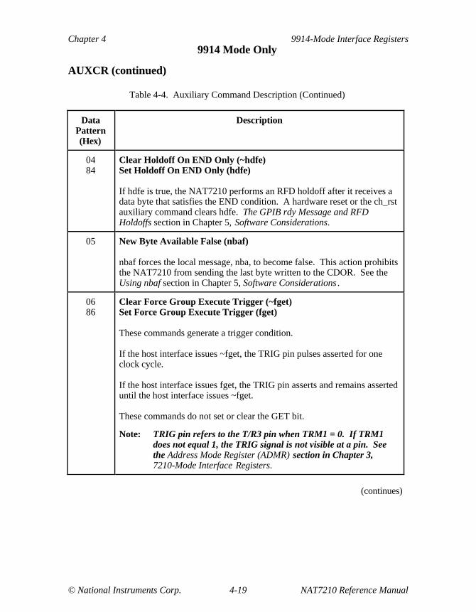
Chapter 4 9914-Mode Interface Registers9914 Mode Only
© National Instruments Corp. 4-19 NAT7210 Reference Manual
AUXCR (continued)
Table 4-4. Auxiliary Command Description (Continued)
DataPattern(Hex)
Description
0484
Clear Holdoff On END Only (~hdfe)Set Holdoff On END Only (hdfe)
If hdfe is true, the NAT7210 performs an RFD holdoff after it receives adata byte that satisfies the END condition. A hardware reset or the ch_rstauxiliary command clears hdfe. The GPIB rdy Message and RFDHoldoffs section in Chapter 5, Software Considerations.
05 New Byte Available False (nbaf)
nbaf forces the local message, nba, to become false. This action prohibitsthe NAT7210 from sending the last byte written to the CDOR. See theUsing nbaf section in Chapter 5, Software Considerations .
0686
Clear Force Group Execute Trigger (~fget)Set Force Group Execute Trigger (fget)
These commands generate a trigger condition.
If the host interface issues ~fget, the TRIG pin pulses asserted for oneclock cycle.
If the host interface issues fget, the TRIG pin asserts and remains asserteduntil the host interface issues ~fget.
These commands do not set or clear the GET bit.
Note: TRIG pin refers to the T/R3 pin when TRM1 = 0. If TRM1does not equal 1, the TRIG signal is not visible at a pin. Seethe Address Mode Register (ADMR) section in Chapter 3,7210-Mode Interface Registers.
(continues)

9914-Mode Interface Registers Chapter 49914 Mode Only
NAT7210 Reference Manual 4-20 © National Instruments Corp.
AUXCR (continued)
Table 4-4. Auxiliary Command Description (Continued)
DataPattern(Hex)
Description
0787
Clear Return To Local (~rtl)Set Return To Local (rtl)
These commands set and clear the IEEE 488 rtl local message. Ahardware reset or the ch_rst auxiliary command also clears rtl.
If the host interface issues the ~rtl command, the IEEE 488 rtl messagepulses true.
If the host interface issues the rtl command, the IEEE 488 rtl messagebecomes true and remains true until the host interface issues ~rtl.
08 Send EOI With The Next Byte (feoi)
The Send EOI command causes the GPIB EOI line to go true with thenext data byte transmitted.
0989
Clear Listen Only (~lon)Set Listen Only (lon)
lon forces the Listener function into the Listener Active state. ~lon forcesthe Listener function to leave the Listener Active state. The local messagepon clears lon.
0A8A
Clear Talk Only (~ton)Set Talk Only (ton)
ton forces the Talker function into the Talker Active state. ~ton forces theTalker function to leave the Talker Active state. The local message ponclears ton.
0B Go To Standby (gts)
The gts command pulses the local gts message. If the NAT7210 is theActive Controller, gts causes the NAT7210 to become the StandbyController and to unassert the GPIB ATN signal. See the Three BasicController States section in Chapter 6, Controller SoftwareConsiderations.
(continues)

Chapter 4 9914-Mode Interface Registers9914 Mode Only
© National Instruments Corp. 4-21 NAT7210 Reference Manual
AUXCR (continued)
Table 4-4. Auxiliary Command Description (Continued)
DataPattern(Hex)
Description
0C Take Control Asynchronously (tca)
The tca command pulses the local tca message. If the NAT7210 is theStandby Controller, tca causes the NAT7210 to become the ActiveController and to assert the GPIB ATN signal.
0D Take Control Synchronously (tcs)
The tcs command pulses the local tcs message. If the NAT7210 is theStandby Controller and an Active Listener, the tcs message causes theNAT7210 to become the Active Controller when the NAT7210 performsan RFD holdoff (that is, the AH function enters ANRS).
0E8E
Clear Request Parallel Poll (~rpp)Set Request Parallel Poll (rpp)
The ~rpp and rpp commands set and clear the local rpp message. Ahardware reset or the ch_rst auxiliary command also clears rpp. If theNAT7210 is the Active Controller, the rpp message causes the NAT7210to send the IDY message to all GPIB devices in the system and to conducta parallel poll. After the NAT9914 has been conducting a parallel poll forat least 2 µs, the control program can read the Command Pass ThroughRegister (CPTR) to obtain the parallel poll result, then the controlprogram can end the parallel poll by issuing the ~rpp command.
0F8F
Clear Send Interface Clear (~sic)Set Send Interface Clear (sic)
The ~sic and sic commands clear and set the sic and rsc local messages.A hardware reset or the ch_rst auxiliary command also clears sic. Settingsic and rsc causes the NAT7210 to become the System Controller and toassert the GPIB Interface Clear (IFC) signal. The control program mustnot issue the ~sic command until after IFC has been asserted at least 100µs. See the System Controller Considerations section in Chapter 6,Controller Software Considerations.
Note: Before it issues the sic command, the control program mustensure—by some means external to the NAT7210—that theGPIB transceivers are enabled to drive the GPIB IFC* signal.
(continues)

9914-Mode Interface Registers Chapter 49914 Mode Only
NAT7210 Reference Manual 4-22 © National Instruments Corp.
AUXCR (continued)
Table 4-4. Auxiliary Command Description (Continued)
DataPattern(Hex)
Description
1090
Clear Send Remote Enable (~sre)Set Send Remote Enable (sre)
The ~sre and sre commands clear and set the sre and rsc local messages.A hardware reset or the ch_rst auxiliary command also clears sre. Settingsre and rsc causes the NAT7210 to become the System Controller and toassert the GPIB REN signal. The control program must not issue the srecommand until after REN has been unasserted at least 100 µs. RemoteEnable (REN) signal. The control program must not issue the srecommand until after REN has been unasserted at least 100 µs. See theSystem Controller Considerations section in Chapter 6, ControllerSoftware Considerations.
Note: Before it issues the sre command, the control program mustensure—by some means external to the NAT7210—that theGPIB transceivers are enabled to drive the GPIB REN* signal.
11 Request Control (rqc)
If the NAT7210 is in the Idle Controller State, the rqc command forcesthe NAT7210 to become the Active Controller when it detects that theATN signal is unasserted.
12 Release Control (rlc)
The rlc command forces the NAT7210 to become an Idle Controller andto unassert ATN.
1393
Clear Disable IMR2, IMR1, And IMR0 Interrupts (~dai)Set Disable IMR2, IMR1, And IMR0 Interrupts (dai)
Issuing dai disables the interrupt pin. The Interrupt Status Registers andany holdoffs selected in the Interrupt Mask Register are not affected bythe dai command. A hardware reset or the ch_rst auxiliary commandclears dai. See the Generating Hardware Interrupts section in Chapter 5,Software Considerations.
(continues)
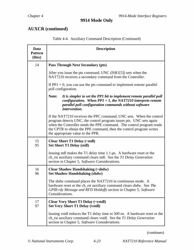
Chapter 4 9914-Mode Interface Registers9914 Mode Only
© National Instruments Corp. 4-23 NAT7210 Reference Manual
AUXCR (continued)
Table 4-4. Auxiliary Command Description (Continued)
DataPattern(Hex)
Description
14 Pass Through Next Secondary (pts)
After you issue the pts command, UNC (ISR1[5]) sets when theNAT7210 receives a secondary command from the Controller.
If PP1 = 0, you can use the pts command to implement remote parallelpoll configuration.
Note: It is simpler to set the PP1 bit to implement remote parallel pollconfiguration. When PP1 = 1, the NAT7210 interprets remoteparallel poll configuration commands without softwareintervention.
If the NAT7210 receives the PPC command, UNC sets. When the controlprogram detects UNC, the control program issues pts. UNC sets againwhen the Controller sends the PPE command. The control program readsthe CPTR to obtain the PPE command, then the control program writesthe appropriate value to the PPR.
1595
Clear Short T1 Delay (~stdl)Set Short T1 Delay (stdl)
Issuing stdl makes the T1 delay time 1.1 µs. A hardware reset or thech_rst auxiliary command clears stdl. See the T1 Delay Generationsection in Chapter 5, Software Considerations.
1696
Clear Shadow Handshaking (~shdw)Set Shadow Handshaking (shdw)
The shdw command places the NAT7210 in continuous mode. Ahardware reset or the ch_rst auxiliary command clears shdw. See TheGPIB rdy Message and RFD Holdoffs section in Chapter 5, SoftwareConsiderations.
1797
Clear Very Short T1 Delay (~vstdl)Set Very Short T1 Delay (vstdl)
Issuing vstdl reduces the T1 delay time to 500 ns. A hardware reset or thech_rst auxiliary command clears vstdl. See the T1 Delay Generationsection in Chapter 5, Software Considerations.
(continues)

9914-Mode Interface Registers Chapter 49914 Mode Only
NAT7210 Reference Manual 4-24 © National Instruments Corp.
AUXCR (continued)
Table 4-4. Auxiliary Command Description (Continued)
DataPattern(Hex)
Description
1898
Clear Request Service bit 2 (~rsv2)Set Request Service bit 2 (rsv2)
The rsv2 bit performs the same function as the rsv bit in the SPMR, but itprovides a means of requesting service that is independent of the SPMR.With rsv2, you can make minor updates to the SPMR without affectingthe state of service request. rsv2 is cleared when the serial poll status byteis sent to the Controller during a serial poll (SPAS & APRS & STRS). Ahardware reset or the ch_rst auxiliary command also clears rsv2.
99 Switch To 7210 Mode (sw7210)
Issuing sw7210 places the NAT7210 into 7210 compatibility mode.
1A9A
Request rsv False (reqf)Request rsv True (reqt)
The reqt and reqf commands are inputs to the IEEE 488.2 Service RequestSynchronization Circuit. Use these commands to set and clear the localrsv message. The local message pon clears reqf and reqt.
If STBO IE = 0, reqt and reqf are not issued immediately; they are issuedon the write of the SPMR that follows the issuing of the reqt or reqfauxiliary command.
If STBO IE = 1, reqt and reqf are issued immediately. The local messagepon clears reqf and reqt. See the IEEE 488.2 Service Requesting sectionin Chapter 5, Software Considerations .
(continues)

Chapter 4 9914-Mode Interface Registers9914 Mode Only
© National Instruments Corp. 4-25 NAT7210 Reference Manual
AUXCR (continued)
Table 4-4. Auxiliary Command Description (Continued)
DataPattern(Hex)
Description
1C Chip Reset (ch_rst)
The Chip Reset command resets the NAT7210 to the followingconditions:
• The local swrst message is set and the interface functions are placed in their idle states.
• SPMR bits are cleared.
• EOS and NL bits are cleared.
• ACCRA, ACCRB, ACCRE, ACCRF, and ACCRI registers are cleared.
• The Parallel Poll Flag local message is cleared.
• The ulpa bit is cleared.
1D9D
Clear Parallel Poll Flag (~ist)Set Parallel Poll Flag (ist)
The ~ist and ist commands set and clear the Parallel Poll Flag. The valueof the Parallel Poll Flag is used as the local ist message when bit four ofAccessory Register B (ISS) = 0. The value of SRQS is used as the localist message when ISS = 1. A hardware reset or the ch_rst auxiliarycommand clears ist.
1E Page-In Interrupt Mask Register 2 (piimr2)
Issuing piimr2 maps Interrupt Mask Register 2 (IMR2) to the ADSRoffset. After this command is issued, you can access IMR2 at the ADSRoffset until one of the following events occurs:
• A hardware reset occurs.
• The ch_rst auxiliary command is issued.
• Another register is paged into the ADSR offset.
• The Clear Page-In auxiliary command is issued.
(continues)

9914-Mode Interface Registers Chapter 49914 Mode Only
NAT7210 Reference Manual 4-26 © National Instruments Corp.
AUXCR (continued)
Table 4-4. Auxiliary Command Description (Continued)
DataPattern(Hex)
Description
1F Page-In Bus Control Register (pibcr)
Issuing pibcr maps the Bus Control Register (BCR) to the ADSR offset.After this command is issued, you can access BCR at the ADSR offsetuntil one of the following events occurs:
• A hardware reset occurs.
• The ch_rst auxiliary command is issued.
• Another register is paged into the ADSR offset.
• The Clear Page-In auxiliary command is issued.
9C Clear Page-In Registers (clrpi)
Issuing clrpi removes the previously paged-in Accessory Register fromthe ADSR offset. After this command is issued, writes to offset 2 have noeffect until a Page-In auxiliary command is issued.
9E Page-In End-of-String Register (pieosr)
Issuing pieosr maps the EOSR to the ADSR offset. After this command isissued, you can access the EOSR at the ADSR offset until one of thefollowing events occurs:
• A hardware reset occurs.
• The ch_rst auxiliary command is issued.
• Another register is paged into the ADSR offset.
• The Clear Page-In auxiliary command is issued.
(continues)
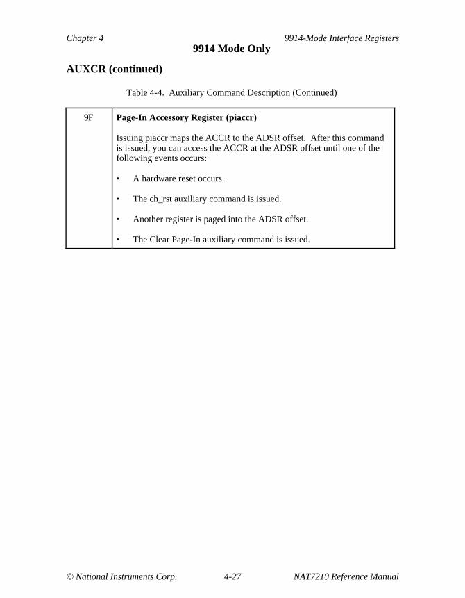
Chapter 4 9914-Mode Interface Registers9914 Mode Only
© National Instruments Corp. 4-27 NAT7210 Reference Manual
AUXCR (continued)
Table 4-4. Auxiliary Command Description (Continued)
9F Page-In Accessory Register (piaccr)
Issuing piaccr maps the ACCR to the ADSR offset. After this commandis issued, you can access the ACCR at the ADSR offset until one of thefollowing events occurs:
• A hardware reset occurs.
• The ch_rst auxiliary command is issued.
• Another register is paged into the ADSR offset.
• The Clear Page-In auxiliary command is issued.

9914-Mode Interface Registers Chapter 49914 Mode Only
NAT7210 Reference Manual 4-28 © National Instruments Corp.
Bus Control Register (BCR)/Bus Status Register (BSR)
Attributes: Write only (BCR)Read only (BSR)
7 6 5 4 3 2 1 0
ATN DAV NDAC NRFD EOI SRQ IFC REN
ATN DAV NDAC NRFD EOI SRQ IFC REN
Bit Mnemonic Description
7r ATN GPIB Attention Status bit7w ATN GPIB Attention Control bit
6r DAV GPIB Data Valid Status bit6w DAV GPIB Data Valid Control bit
5r NDAC GPIB Not Data Accepted Status bit5w NDAC GPIB Not Data Accepted Control bit
4r NRFD GPIB Not Ready For Data Status bit4w NRFD GPIB Not Ready For Data Control bit
3r EOI GPIB End-or-Identify Status bit3w EOI GPIB End-or-Identify Control bit
2r SRQ GPIB Service Request Status bit2w SRQ GPIB Service Request Control bit
1r IFC GPIB Interface Clear Status bit1w IFC GPIB Interface Clear Control bit
0r REN GPIB Remote Enable Status bit0w REN GPIB Remote Enable Control bit
Reads of the Bus Status Register (BSR) return the status of the GPIB control lines at thetime of the read. Write ones to bits in the Bus Control Register (BCR) to assert thecorresponding GPIB control lines.

Chapter 4 9914-Mode Interface Registers9914 Mode Only
© National Instruments Corp. 4-29 NAT7210 Reference Manual
BCR/BSR (continued)
Because the NAT7210 is either transmitting or receiving a GPIB control line at anyparticular time and is not performing both actions simultaneously, setting a bit in theBCR may not automatically assert the corresponding line on the GPIB. If the NAT7210is transmitting a GPIB line when the corresponding bit in the BCR is set, the NAT7210asserts the GPIB line. If the NAT7210 is receiving a GPIB line when the correspondingbit in the BCR is set, the GPIB line is not asserted. However, in both these cases, theGPIB signal internal to the NAT7210 is logically ORed with the value of the BCR bit.Figure 4-1 illustrates the GPIB input/output hardware configuration.
eliminatesglitches inREN & IFC
GPIB Line In
BCR Bit
Transmit Enable
GPIB Line Out
NDAC NRFDSRQ
PIN
Figure 4-1. GPIB I/O Hardware Configuration
In Figure 4-1, Transmit Enable represents the internal signal that is true when the chip isdriving a particular GPIB control line. GPIB Line Out represents the internal signal thatis true when an interface function within the chip is attempting to assert a GPIB controlsignal. BCR Bit corresponds to the bit in the BCR. GPIB Line In represents the internalGPIB lines that are inputs to the GPIB interface functions and the BSR. The internalsignals SRQ , NDAC, and NRFD are monitored by the interface functions even when theyare not driven onto the pin. For this reason, the internal value of these signals is ORedwith the external value.
Because the BSR samples the GPIB control lines from the GPIB transceiver—not theactual GPIB bus—the direction of each line determines the validity of each bit.Generally, when a signal is an input, the BSR reflects its true bus status, while an outputsignal reflects only the NAT7210 value of that particular line. Under normal GPIBoperation, this restriction on the validity of the BSR should not be too limiting, becausethe lines that are typically monitored are valid when they are monitored. For example,the SRQ line is valid in the BSR when the NAT7210 is CIC, which is also when the SRQline will be monitored.

9914-Mode Interface Registers Chapter 49914 Mode Only
NAT7210 Reference Manual 4-30 © National Instruments Corp.
Command/Data Out Register (CDOR)
Attributes: Write only
7 6 5 4 3 2 1 0
DIO8 DIO7 DIO6 DIO5 DIO4 DIO3 DIO2 DIO1
Bit Mnemonic Description
7–0w DIO[8–1] GPIB data lines DIO[8–1]
The CDOR moves data from the CPU to the GPIB whenthe interface is the GPIB Talker or Controller. Writing tothe CDOR sets the local message, nba. When nba is true,the Source Handshake (SH) function can transfer the dataor command in the CDOR to other GPIB devices.Writing to the CDOR also
• Clears the Byte Out (BO) bit.
• Clears the DRQ signal (unless DMAE = 1 andDMAO = 0).
The host interface can write to the CDOR at offset 7 or byperforming a DMA write operation.
The CDOR and the DIR use separate latches. A read ofthe DIR does not change data in the CDOR. The CDORis a transparent latch; thus, the GPIB data bus (DIO(8–1))reflects changes on the CPU data bus during write cyclesto the CDOR.
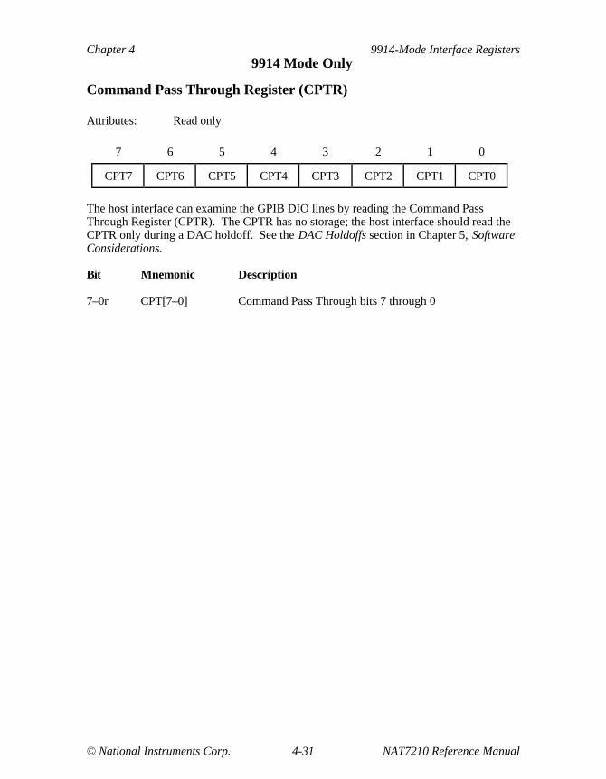
Chapter 4 9914-Mode Interface Registers9914 Mode Only
© National Instruments Corp. 4-31 NAT7210 Reference Manual
Command Pass Through Register (CPTR)
Attributes: Read only
7 6 5 4 3 2 1 0
CPT7 CPT6 CPT5 CPT4 CPT3 CPT2 CPT1 CPT0
The host interface can examine the GPIB DIO lines by reading the Command PassThrough Register (CPTR). The CPTR has no storage; the host interface should read theCPTR only during a DAC holdoff. See the DAC Holdoffs section in Chapter 5, SoftwareConsiderations.
Bit Mnemonic Description
7–0r CPT[7–0] Command Pass Through bits 7 through 0
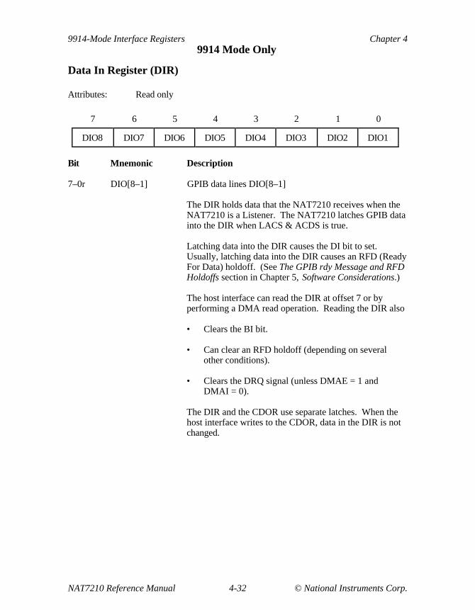
9914-Mode Interface Registers Chapter 49914 Mode Only
NAT7210 Reference Manual 4-32 © National Instruments Corp.
Data In Register (DIR)
Attributes: Read only
7 6 5 4 3 2 1 0
DIO8 DIO7 DIO6 DIO5 DIO4 DIO3 DIO2 DIO1
Bit Mnemonic Description
7–0r DIO[8–1] GPIB data lines DIO[8–1]
The DIR holds data that the NAT7210 receives when theNAT7210 is a Listener. The NAT7210 latches GPIB datainto the DIR when LACS & ACDS is true.
Latching data into the DIR causes the DI bit to set.Usually, latching data into the DIR causes an RFD (ReadyFor Data) holdoff. (See The GPIB rdy Message and RFDHoldoffs section in Chapter 5, Software Considerations.)
The host interface can read the DIR at offset 7 or byperforming a DMA read operation. Reading the DIR also
• Clears the BI bit.
• Can clear an RFD holdoff (depending on severalother conditions).
• Clears the DRQ signal (unless DMAE = 1 andDMAI = 0).
The DIR and the CDOR use separate latches. When thehost interface writes to the CDOR, data in the DIR is notchanged.
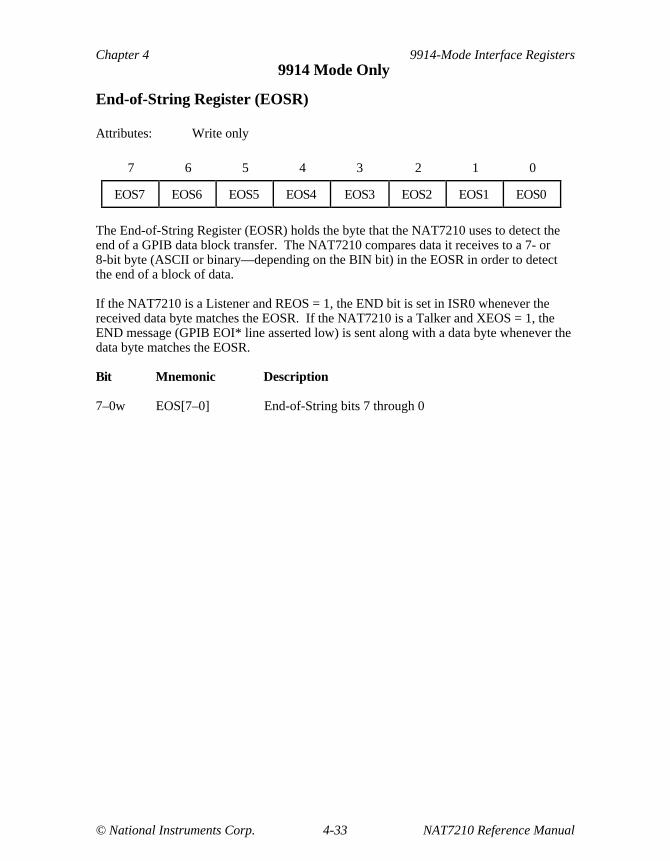
Chapter 4 9914-Mode Interface Registers9914 Mode Only
© National Instruments Corp. 4-33 NAT7210 Reference Manual
End-of-String Register (EOSR)
Attributes: Write only
7 6 5 4 3 2 1 0
EOS7 EOS6 EOS5 EOS4 EOS3 EOS2 EOS1 EOS0
The End-of-String Register (EOSR) holds the byte that the NAT7210 uses to detect theend of a GPIB data block transfer. The NAT7210 compares data it receives to a 7- or8-bit byte (ASCII or binary—depending on the BIN bit) in the EOSR in order to detectthe end of a block of data.
If the NAT7210 is a Listener and REOS = 1, the END bit is set in ISR0 whenever thereceived data byte matches the EOSR. If the NAT7210 is a Talker and XEOS = 1, theEND message (GPIB EOI* line asserted low) is sent along with a data byte whenever thedata byte matches the EOSR.
Bit Mnemonic Description
7–0w EOS[7–0] End-of-String bits 7 through 0

9914-Mode Interface Registers Chapter 49914 Mode Only
NAT7210 Reference Manual 4-34 © National Instruments Corp.
Internal Count Register (ICR)
Attributes: Write only
7 6 5 4 3 2 1 0
0 0 1 0 F3 F2 F1 F0
The Internal Count Register (ICR) determines the internal clock frequency of theNAT7210. You write to the ICR at the same offset as the ACCR.
Note: The ICR resets to 00101000 (8 MHz).
Bit Mnemonic Description
3–0 F(3–0) Clock Frequency
These bits, in addition to MICR (ICR2[0]), determine thelength of certain delays that are required by theIEEE 488 standard. You should set these bits accordingto the frequency of the signal driving the CLK pin. Forproper operation, set F(3–0) and MICR as follows:
ClockFrequency
MICR F(3–0)
1 0 0001
2 0 0010
3 0 0011
4 0 0100
5 0 0101
6 0 0110
7 0 0111
8 0 1000
10 1 0101
16 1 1000
20 1 1010

Chapter 4 9914-Mode Interface Registers9914 Mode Only
© National Instruments Corp. 4-35 NAT7210 Reference Manual
Interrupt Mask Register 0 (IMR0)
Attributes: Write only
7 6 5 4 3 2 1 0
DMAO DMAI BI IE BO IE END IE SPAS IE RLC IE MAC IE
Interrupt Status Register 0 (ISR0)
Attributes: Read onlyBits are cleared when read
7 6 5 4 3 2 1 0
INT0 INT1 BI BO END SPAS RLC MAC
Interrupt Status Register 0 (ISR0) contains Interrupt Status bits. Interrupt MaskRegister 0 (IMR0) contains Interrupt Enable bits that directly correspond to the InterruptStatus bits in ISR0. As a result, ISR0 and IMR0 service six possible interrupt conditions;each condition has an associated Interrupt Status bit and an Interrupt Enable bit. If anInterrupt Enable bit is true when the corresponding status condition or event occurs, theNAT7210 can generate a hardware interrupt request. See the Generating HardwareInterrupts section in Chapter 5, Software Considerations .
Bits in ISR0 are set and cleared regardless of the status of the Interrupt bits in IMR0.If an interrupt condition occurs at the same time the host interface is reading ISR0, theNAT7210 does not set the corresponding Interrupt Status bit until the read is finished.A hardware reset clears all bits in IMR0.
Bit Mnemonic Description
7r INT0 Interrupt Register 0 Interrupt bit
INT0 is set when an unmasked status bit in ISR0 is set.
7w DMAO DMA Output Enable bit
If DMAE = 1 (ACCRI[0]), DMAO enables the NAT7210to assert the DRQ pin as a GPIB Talker. The NAT7210asserts DRQ when it is ready to accept another byte in theCDOR. DRQ does not assert if the NAT7210 is not aTalker.
If DMAE = 0, write 0 to DMAO.

9914-Mode Interface Registers Chapter 49914 Mode Only
NAT7210 Reference Manual 4-36 © National Instruments Corp.
IMR0/ISR0 (continued)
Bit Mnemonic Description
6r INT1 Interrupt Register 1 Interrupt bit
INT1 is set when an unmasked status bit in InterruptStatus Register 1 (ISR1) is set.
6w DMAI DMA Input Enable bit
If DMAE = 1 (ACCRI[0]), DMAI enables the NAT7210to assert the DRQ pin as a GPIB Listener. The NAT7210asserts DRQ when the DIR contains a byte for the hostinterface to read.
If DMAE = 0, write 0 to DMAI.
5r BI Byte In bit5w BI IE Byte In Interrupt Enable bit
BI indicates that a data byte has been received in the DataIn Register. An RFD holdoff must be cleared before theNAT7210 accepts the next data byte.
BI is set byLACS & ACDS & ~(continuous mode)
BI is cleared byswrst + (read ISR0) + (read DIR)
4r BO Byte Out bit4w BO IE Byte Out Interrupt Enable bit
BO indicates that the NAT7210 is the Active Controlleror Talker and that the CDOR does not contain a byte tosend over the GPIB. BO sets again after each byte hasbeen sent and the source handshake has returned toSGNS.
BO is set by(CACS + TACS) & SGNS & ~nba
BO is cleared byswrst + (read ISR0) + (write CDOR)
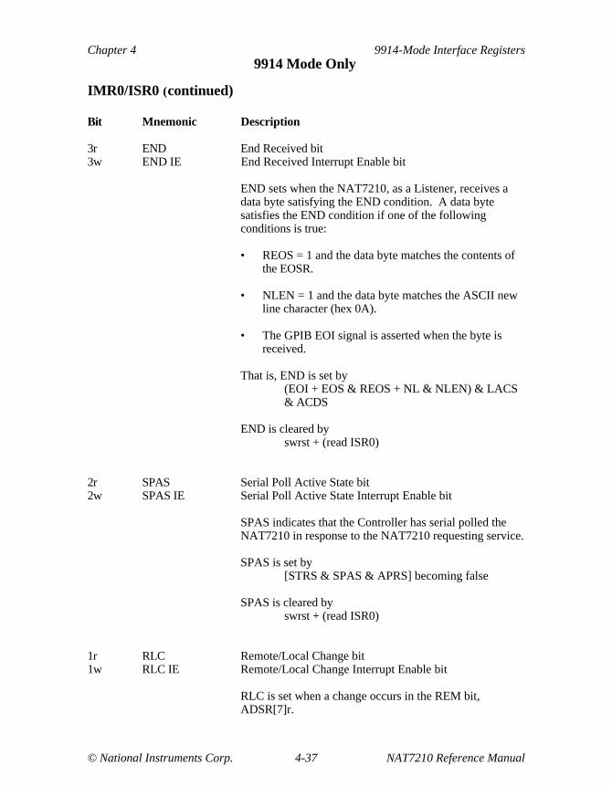
Chapter 4 9914-Mode Interface Registers9914 Mode Only
© National Instruments Corp. 4-37 NAT7210 Reference Manual
IMR0/ISR0 (continued)
Bit Mnemonic Description
3r END End Received bit3w END IE End Received Interrupt Enable bit
END sets when the NAT7210, as a Listener, receives adata byte satisfying the END condition. A data bytesatisfies the END condition if one of the followingconditions is true:
• REOS = 1 and the data byte matches the contents ofthe EOSR.
• NLEN = 1 and the data byte matches the ASCII newline character (hex 0A).
• The GPIB EOI signal is asserted when the byte isreceived.
That is, END is set by(EOI + EOS & REOS + NL & NLEN) & LACS& ACDS
END is cleared byswrst + (read ISR0)
2r SPAS Serial Poll Active State bit2w SPAS IE Serial Poll Active State Interrupt Enable bit
SPAS indicates that the Controller has serial polled theNAT7210 in response to the NAT7210 requesting service.
SPAS is set by[STRS & SPAS & APRS] becoming false
SPAS is cleared byswrst + (read ISR0)
1r RLC Remote/Local Change bit1w RLC IE Remote/Local Change Interrupt Enable bit
RLC is set when a change occurs in the REM bit,ADSR[7]r.

9914-Mode Interface Registers Chapter 49914 Mode Only
NAT7210 Reference Manual 4-38 © National Instruments Corp.
IMR0/ISR0 (continued)
Bit Mnemonic Description
RLC is cleared byswrst + (read ISR0)
0r MAC My Address Change bit0w MAC IE My Address Change Interrupt Enable bit
MAC indicates that the NAT7210 has received acommand from the Controller and that this command haschanged the addressed state of the NAT7210.
If the NAT7210 is using secondary addressing, MAC setsonly when the NAT7210 becomes unaddressed. Ifedpa = 1, MAC does not set when the Controllerreaddresses the NAT7210 at the NAT7210’s otherprimary address.
MAC is set byACDS & (MTA & ~TADS & ~APT IE+ OTA & TADS+ MLA & ~LADS & ~APT IE+ UNL & LADS)
MAC is cleared byswrst + (read ISR0)
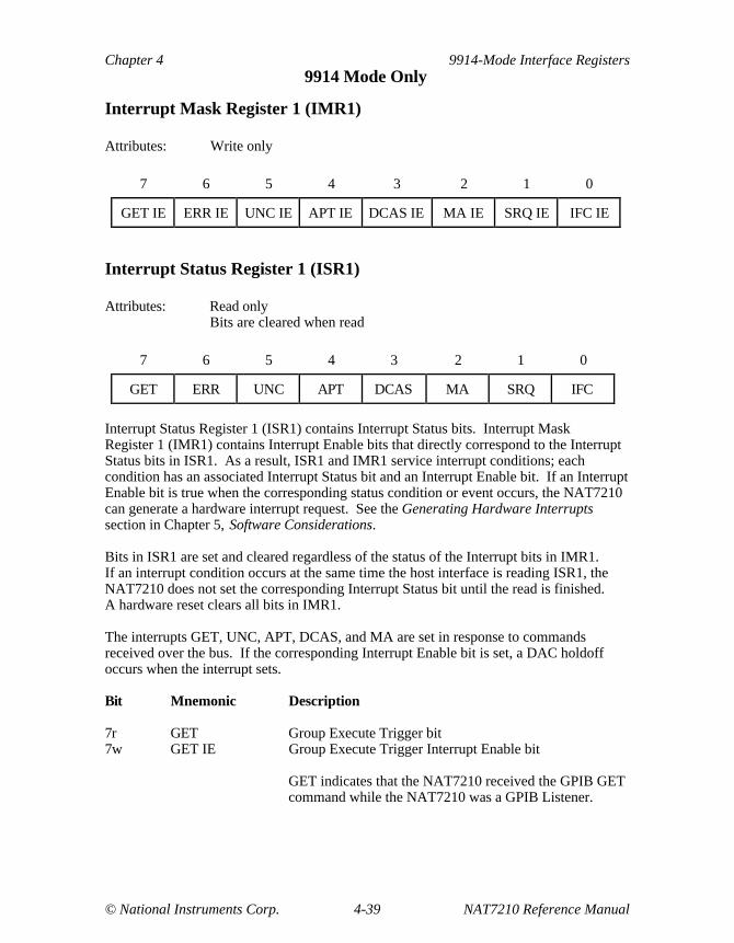
Chapter 4 9914-Mode Interface Registers9914 Mode Only
© National Instruments Corp. 4-39 NAT7210 Reference Manual
Interrupt Mask Register 1 (IMR1)
Attributes: Write only
7 6 5 4 3 2 1 0
GET IE ERR IE UNC IE APT IE DCAS IE MA IE SRQ IE IFC IE
Interrupt Status Register 1 (ISR1)
Attributes: Read onlyBits are cleared when read
7 6 5 4 3 2 1 0
GET ERR UNC APT DCAS MA SRQ IFC
Interrupt Status Register 1 (ISR1) contains Interrupt Status bits. Interrupt MaskRegister 1 (IMR1) contains Interrupt Enable bits that directly correspond to the InterruptStatus bits in ISR1. As a result, ISR1 and IMR1 service interrupt conditions; eachcondition has an associated Interrupt Status bit and an Interrupt Enable bit. If an InterruptEnable bit is true when the corresponding status condition or event occurs, the NAT7210can generate a hardware interrupt request. See the Generating Hardware Interruptssection in Chapter 5, Software Considerations.
Bits in ISR1 are set and cleared regardless of the status of the Interrupt bits in IMR1.If an interrupt condition occurs at the same time the host interface is reading ISR1, theNAT7210 does not set the corresponding Interrupt Status bit until the read is finished.A hardware reset clears all bits in IMR1.
The interrupts GET, UNC, APT, DCAS, and MA are set in response to commandsreceived over the bus. If the corresponding Interrupt Enable bit is set, a DAC holdoffoccurs when the interrupt sets.
Bit Mnemonic Description
7r GET Group Execute Trigger bit7w GET IE Group Execute Trigger Interrupt Enable bit
GET indicates that the NAT7210 received the GPIB GETcommand while the NAT7210 was a GPIB Listener.

9914-Mode Interface Registers Chapter 49914 Mode Only
NAT7210 Reference Manual 4-40 © National Instruments Corp.
IMR1/ISR1 (continued)
Bit Mnemonic Description
If GET IE = 1, a DAC holdoff occurs when the interruptcondition occurs. The TRIG pin goes high when theinterrupt condition occurs and remains high until the DACholdoff is released.
If GET IE = 0, the TRIG pin pulses high.
GET is set byGET & LADS & ACDS
GET is cleared byswrst + (read ISR1)
Note: TRIG pin refers to the T/R3 pin whenTRM1 = 0. If TRM1 does not equal 1, theTRIG signal is not visible at a pin. See theAddress Mode Register (ADMR) section inChapter 3, 7210-Mode Interface Registers.
6r ERR Error bit6w ERR IE Error Interrupt Enable bit
ERR sets when the Source Handshake becomes active(enters SDYS) and finds that the NDAC and NRFD linesare both unasserted on the GPIB. This condition indicatesthat there are no acceptors on the GPIB.
ERR is set bySDYS & EXTDAC & RFD
ERR is cleared byswrst + (read ISR1)
5r UNC Unrecognized Command bit5w UNC IE Unrecognized Command Interrupt Enable bit
UNC flags the occurrence of several types of GPIBcommands. UNC sets when the NAT7210 accepts anyunrecognized Universal Command Group (UCG)command.

Chapter 4 9914-Mode Interface Registers9914 Mode Only
© National Instruments Corp. 4-41 NAT7210 Reference Manual
IMR1/ISR1 (continued)
Bit Mnemonic Description
If the NAT7210 is an addressed Listener, UNC sets whenthe NAT7210 accepts any unrecognized AddressedCommand Group (ACG) command.
UNC flags the first secondary command that theNAT7210 accepts after the host interface issues the PassThrough Next secondary auxiliary command. UNC canalso flag the occurrence of commands that you specifywhen you set the AUXRE[3–2]w or AUXRF[3–0]w bits.
If UNC IE = 1, the NAT7210 performs a DAC holdoffwhen UNC sets. The host interface releases the DACholdoff by issuing the Release DAC Holdoff auxiliarycommand. Read undefined commands by using theCommand Pass Through Register (CPTR).
UNC is set byACDS & UCG & ~(LLO + SPE + SPD + DCL +
PPU & PP1)+ ACDS & ACG & ~(GET + GTL
+ SDC + TCT + PPC & PP1) & LADS+ SCG & PTS & ACDS+ DHADT & GET & ACDS+ DHADC & (SDC + DCL) & ACDS+ DHATA & TAG & ~UNT & ACDS+ DHALA & LAG & ~UNL & ACDS + DHUNTL & (UNT + UNL) & ACDS+ DHALL & ATN & ACDS
UNC is cleared byswrst + (read ISR1)
4r APT Address Pass Through bit4w APT IE Address Pass Through Interrupt Enable bit
Setting APT IE enables secondary addressing. If the lastprimary command accepted was a primary talk or listenaddress of the NAT7210, APT sets when the NAT7210accepts a secondary command. The secondary commandis a secondary GPIB address that can be read in theCPTR.
Note: When the host interface uses secondaryaddressing, it must check APT.

9914-Mode Interface Registers Chapter 49914 Mode Only
NAT7210 Reference Manual 4-42 © National Instruments Corp.
IMR1/ISR1 (continued)
Bit Mnemonic Description
If APT IE = 1, the NAT7210 performs a DAC holdoffwhen APT sets. The host interface releases the DACholdoff by issuing the Release DAC Holdoff auxiliarycommand.
APT is set by(TPAS + LPAS) & SCG & ACDS
APT is cleared byswrst + (read ISR1)
3r DCAS Device Clear Active State bit3w DCAS IE Device Clear Active State Interrupt Enable bit
DCAS indicates that either the NAT7210 received theGPIB Device Clear (DCL) command or that theNAT7210 was a Listener and received the GPIB SelectedDevice Clear (SDC) command.
If DCAS IE = 1, the NAT7210 performs a DAC holdoffwhen DCAS sets. The host interface releases the DACholdoff by issuing the Release DAC Holdoff auxiliarycommand.
DCAS is set byACDS & (DCL + SDC & LADS)
DCAS is cleared byswrst + (read ISR1)
2r MA My Address bit2w MA IE My Address Interrupt Enable bit
MA sets when the NAT7210 accepts its primary talk orlisten address.
If MA IE = 1, the NAT7210 performs a DAC holdoffwhen MA sets. The host interface releases the DACholdoff by issuing the Release DAC Holdoff auxiliarycommand.
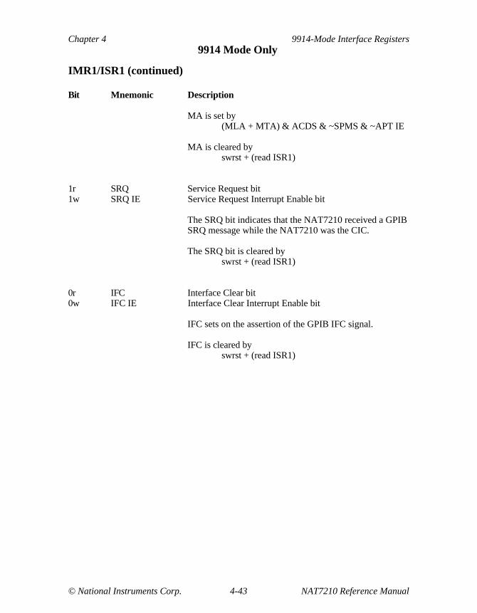
Chapter 4 9914-Mode Interface Registers9914 Mode Only
© National Instruments Corp. 4-43 NAT7210 Reference Manual
IMR1/ISR1 (continued)
Bit Mnemonic Description
MA is set by(MLA + MTA) & ACDS & ~SPMS & ~APT IE
MA is cleared byswrst + (read ISR1)
1r SRQ Service Request bit1w SRQ IE Service Request Interrupt Enable bit
The SRQ bit indicates that the NAT7210 received a GPIBSRQ message while the NAT7210 was the CIC.
The SRQ bit is cleared byswrst + (read ISR1)
0r IFC Interface Clear bit0w IFC IE Interface Clear Interrupt Enable bit
IFC sets on the assertion of the GPIB IFC signal.
IFC is cleared byswrst + (read ISR1)
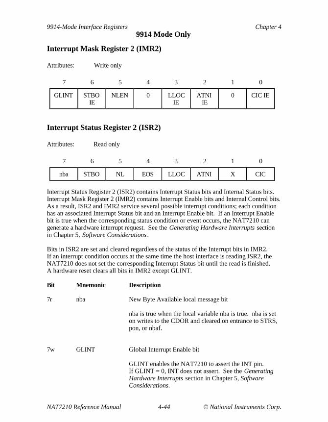
9914-Mode Interface Registers Chapter 49914 Mode Only
NAT7210 Reference Manual 4-44 © National Instruments Corp.
Interrupt Mask Register 2 (IMR2)
Attributes: Write only
7 6 5 4 3 2 1 0
GLINT STBOIE
NLEN 0 LLOCIE
ATNIIE
0 CIC IE
Interrupt Status Register 2 (ISR2)
Attributes: Read only
7 6 5 4 3 2 1 0
nba STBO NL EOS LLOC ATNI X CIC
Interrupt Status Register 2 (ISR2) contains Interrupt Status bits and Internal Status bits.Interrupt Mask Register 2 (IMR2) contains Interrupt Enable bits and Internal Control bits.As a result, ISR2 and IMR2 service several possible interrupt conditions; each conditionhas an associated Interrupt Status bit and an Interrupt Enable bit. If an Interrupt Enablebit is true when the corresponding status condition or event occurs, the NAT7210 cangenerate a hardware interrupt request. See the Generating Hardware Interrupts sectionin Chapter 5, Software Considerations .
Bits in ISR2 are set and cleared regardless of the status of the Interrupt bits in IMR2.If an interrupt condition occurs at the same time the host interface is reading ISR2, theNAT7210 does not set the corresponding Interrupt Status bit until the read is finished.A hardware reset clears all bits in IMR2 except GLINT.
Bit Mnemonic Description
7r nba New Byte Available local message bit
nba is true when the local variable nba is true. nba is seton writes to the CDOR and cleared on entrance to STRS,pon, or nbaf.
7w GLINT Global Interrupt Enable bit
GLINT enables the NAT7210 to assert the INT pin.If GLINT = 0, INT does not assert. See the GeneratingHardware Interrupts section in Chapter 5, SoftwareConsiderations.

Chapter 4 9914-Mode Interface Registers9914 Mode Only
© National Instruments Corp. 4-45 NAT7210 Reference Manual
IMR2/ISR2 (continued)
Bit Mnemonic Description
6r STBO Status Byte Out bit6w STBO IE Status Byte Out Interrupt Enable bit
STBO is set when the NAT7210 enters SPAS whenSTBO IE = 1. After STBO sets, the control programshould write the current STB to the SPMR. The currentSTB is then transmitted to the GPIB as the STB. Writingthe SPMR clears STBO.
STBO IE determines how the NAT7210 requests serviceand responds to serial polls.
If STBO IE = 0, the rsv bit in the SPMR can be used torequest service. When the GPIB Controller serial pollsthe NAT7210, the NAT7210 transmits the current valueof the SPMR.
If STBO IE = 1, the rsv bit in the SPMR has no effect onthe SR1 function and rsv must be generated through thereqt auxiliary command. When the GPIB Controllerserial polls the NAT7210, STBO sets. In response toSTBO, the host interface writes a byte to the SPMR, thenthe NAT7210 transmits this byte as the Serial Pollresponse.
STBO is set bySTBO IE & SPAS
STBO is cleared byswrst + (write SPMR) + ~SPAS
5r NL New Line Receive bit
NL indicates that the last data byte that the NAT7210received was an ASCII new line character.
NL is set byLACS & NL & ACDS
NL is cleared byswrst + (LACS & ~NL & ACDS)
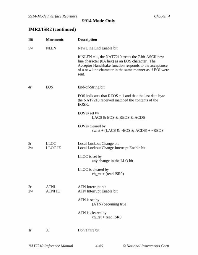
9914-Mode Interface Registers Chapter 49914 Mode Only
NAT7210 Reference Manual 4-46 © National Instruments Corp.
IMR2/ISR2 (continued)
Bit Mnemonic Description
5w NLEN New Line End Enable bit
If NLEN = 1, the NAT7210 treats the 7-bit ASCII newline character (0A hex) as an EOS character. TheAcceptor Handshake function responds to the acceptanceof a new line character in the same manner as if EOI weresent.
4r EOS End-of-String bit
EOS indicates that REOS = 1 and that the last data bytethe NAT7210 received matched the contents of theEOSR.
EOS is set byLACS & EOS & REOS & ACDS
EOS is cleared byswrst + (LACS & ~EOS & ACDS) + ~REOS
3r LLOC Local Lockout Change bit3w LLOC IE Local Lockout Change Interrupt Enable bit
LLOC is set byany change in the LLO bit
LLOC is cleared bych_rst + (read ISR0)
2r ATNI ATN Interrupt bit2w ATNI IE ATN Interrupt Enable bit
ATN is set by(ATN) becoming true
ATN is cleared bych_rst + read ISR0
1r X Don’t care bit

Chapter 4 9914-Mode Interface Registers9914 Mode Only
© National Instruments Corp. 4-47 NAT7210 Reference Manual
IMR2/ISR2 (continued)
Bit Mnemonic Description
0r CIC Controller-In-Charge bit0w CIC IE Controller-In-Charge Interrupt Enable bit
CIC indicates whether the NAT7210 is the Controller-in-Charge.
CIC = ~(CIDS + CADS)
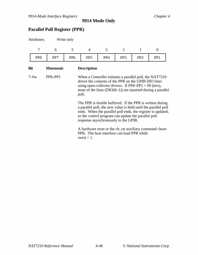
9914-Mode Interface Registers Chapter 49914 Mode Only
NAT7210 Reference Manual 4-48 © National Instruments Corp.
Parallel Poll Register (PPR)
Attributes: Write only
7 6 5 4 3 2 1 0
PP8 PP7 PP6 PP5 PP4 PP3 PP2 PP1
Bit Mnemonic Description
7–0w PP8–PP1 When a Controller initiates a parallel poll, the NAT7210drives the contents of the PPR on the GPIB DIO linesusing open-collector drivers. If PP8–PP1 = 00 (hex),none of the lines (DIO(8–1)) are asserted during a parallelpoll.
The PPR is double buffered. If the PPR is written duringa parallel poll, the new value is held until the parallel pollends. When the parallel poll ends, the register is updated,so the control program can update the parallel pollresponse asynchronously to the GPIB.
A hardware reset or the ch_rst auxiliary command clearsPPR. The host interface can load PPR whileswrst = 1.

Chapter 4 9914-Mode Interface Registers9914 Mode Only
© National Instruments Corp. 4-49 NAT7210 Reference Manual
Serial Poll Mode Register (SPMR)
Attributes: Write only
7 6 5 4 3 2 1 0
S8 rsv/RQS S6 S5 S4 S3 S2 S1
Serial Poll Status Register (SPSR)
Attributes: Read only
7 6 5 4 3 2 1 0
S8 PEND S6 S5 S4 S3 S2 S1
Bit Mnemonic Description
7r, S8 Serial Poll Status bit 87w
5–0r, S[6–1] Serial Poll Status bits 6 through 15–0w
These bits send device- or system-dependent statusinformation over the GPIB when the Controller serialpolls the NAT7210.
When STBO IE = 0, the NAT7210 transmits a byte ofstatus information, SPMR[7–0], to the CIC if the CICserial polls the NAT7210. The SPMR bits S[8, 6–1] aredouble buffered. If the host interface writes to the SPMRduring a serial poll when SPAS is active, the NAT7210saves the value. The NAT7210 updates the SPMR whenthe NAT7210 exits SPAS.
When STBO IE = 1 and the Controller serial polls theNAT7210, the STBO interrupt condition sets. The hostinterface should write the STB and the RQS bit to theSPMR in response to an STBO interrupt.
Issuing the ch_rst auxiliary command clears these bits.

9914-Mode Interface Registers Chapter 49914 Mode Only
NAT7210 Reference Manual 4-50 © National Instruments Corp.
SPMR/SPSR (continued)
Bit Mnemonic Description
6r PEND Pending bit
PEND sets when rsv = 1. PEND clears when theNAT7210 is in the Negative Poll Response State (NPRS)and the local Request Service (rsv) message is false. Byreading the PEND status bit, you can confirm that arequest was accepted and that the Status Byte (STB) wastransmitted (PEND = 0).
6w rsv/RQS Request Service/ RQS bit
When STBO IE = 0, bit 6 is the rsv bit. The rsv bitgenerates the GPIB local rsv message. When rsv = 1 andthe GPIB Controller is not serial polling the NAT7210,the NAT7210 enters the Service Request State (SRQS)and asserts the GPIB SRQ signal. When the Controllerreads the STB during the poll, the NAT7210 clears rsv.The rsv bit is also cleared by a hardware reset or bywriting 0 to it. Issuing the ch_rst auxiliary command alsoclears rsv.
When STBO IE = 1, bit 6 is the RQS bit. When theController serial polls the NAT7210, the STBO interruptcondition sets. The host interface should write the STBand the RQS bit to the SPMR in response to an STBOinterrupt. The NAT7210 transfers the STB and RQS tothe Controller during that particular serial poll. Ahardware reset clears RQS. Issuing the ch_rst auxiliarycommand also clears RQS.

© National Instruments Corp. 5-1 NAT7210 Reference Manual
Chapter 5Software Considerations The chapter explains important NAT7210 programming considerations, including chipinitialization, Talkers and Listeners, message reception, and holdoffs. You should alsorefer to Chapter 6, Controller Software Considerations , for applications that use theNAT7210 GPIB Controller functions.
This chapter, except where explicitly noted, assumes that the NAT7210 uses 7210-modearchitecture and that the reader is familiar with the GPIB. For more information aboutGPIB, refer to Appendix B, Introduction to the GPIB, and the IEEE 488.1 andIEEE 488.2 standard.
Chip Initialization Sequence
1. Place the NAT7210 in 7210 Mode
Place the NAT7210 in 7210 mode by performing one of the following actions:
• Assert the RESET* pin.
• Write the sw7210 command to the AUXCR if the NAT7210 is in 9914 mode.
• Write 99 (hex) to offset 3 if you do not know whether the NAT7210 is in 7210 modeor 9914 mode. If the chip is in 9914 mode, this write places it in 7120 mode. If thechip is already in 7210 mode, this write access writes to the 7210-mode SPMR.
2. Make Sure the Local pon Message Is Asserted
Write the Chip Reset auxiliary command (2 hex) to the AUXMR to assert the local ponmessage. When pon is asserted, the chip is logically disconnected from the GPIB and theGPIB interface functions of the NAT7210 are idle (and ignore GPIB signals).
3. Set the Clock Frequency
Set the clock frequency of the NAT7210 by writing to the ICR and the ICR2.
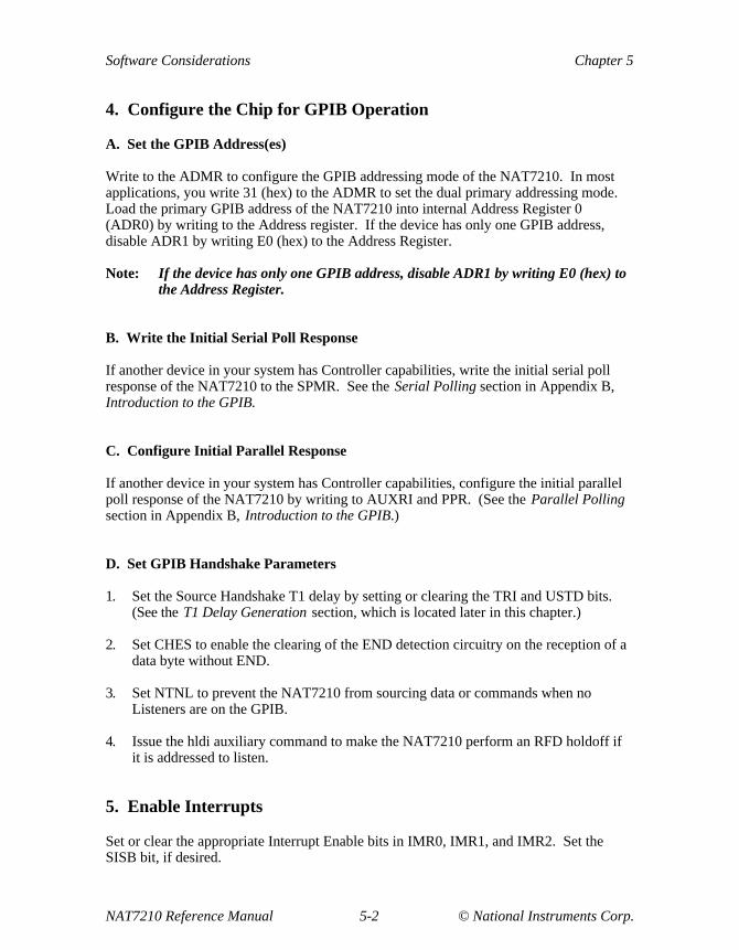
Software Considerations Chapter 5
NAT7210 Reference Manual 5-2 © National Instruments Corp.
4. Configure the Chip for GPIB Operation
A. Set the GPIB Address(es)
Write to the ADMR to configure the GPIB addressing mode of the NAT7210. In mostapplications, you write 31 (hex) to the ADMR to set the dual primary addressing mode.Load the primary GPIB address of the NAT7210 into internal Address Register 0(ADR0) by writing to the Address register. If the device has only one GPIB address,disable ADR1 by writing E0 (hex) to the Address Register.
Note: If the device has only one GPIB address, disable ADR1 by writing E0 (hex) tothe Address Register.
B. Write the Initial Serial Poll Response
If another device in your system has Controller capabilities, write the initial serial pollresponse of the NAT7210 to the SPMR. See the Serial Polling section in Appendix B,Introduction to the GPIB.
C. Configure Initial Parallel Response
If another device in your system has Controller capabilities, configure the initial parallelpoll response of the NAT7210 by writing to AUXRI and PPR. (See the Parallel Pollingsection in Appendix B, Introduction to the GPIB.)
D. Set GPIB Handshake Parameters
1. Set the Source Handshake T1 delay by setting or clearing the TRI and USTD bits.(See the T1 Delay Generation section, which is located later in this chapter.)
2. Set CHES to enable the clearing of the END detection circuitry on the reception of adata byte without END.
3. Set NTNL to prevent the NAT7210 from sourcing data or commands when noListeners are on the GPIB.
4. Issue the hldi auxiliary command to make the NAT7210 perform an RFD holdoff ifit is addressed to listen.
5. Enable Interrupts
Set or clear the appropriate Interrupt Enable bits in IMR0, IMR1, and IMR2. Set theSISB bit, if desired.
Chapter 5 Software Considerations
© National Instruments Corp. 5-3 NAT7210 Reference Manual
6. Clear the Local pon Message
Issue the pon auxiliary command to clear the local pon message and to begin GPIBoperation.
GPIB Talker or Listener Considerations
GPIB Addressing
Logical and Physical Devices
When you connect the NAT7210 to the GPIB by using standard GPIB transceivers, theNAT7210 is one physical GPIB device. The IEEE 488.1 transceiver places a singlephysical device load on the GPIB. The IEEE 488.1 standard specifies that a GPIB systemcontain no more than 15 physical devices.
In most applications, the NAT7210 is also one logical device. However, a single physicalGPIB device can implement more than one logical GPIB device. Each logical devicemust have a unique GPIB address. The NAT7210 can implement up to 961 logical GPIBdevices.
Normal and Extended Addressing
Logical GPIB devices use either normal or extended addressing. With normaladdressing, a GPIB device has a single address; valid addresses are 0 through 30(decimal), inclusive. To address a device to become a Talker or Listener, a Controllersends the talk or listen address of the device. If a device’s address is 6, for example, aController sends the My Talk Address 6 (MTA6) message to address that device tobecome a Talker.
With extended addressing, a GPIB device has two addresses: a primary address and asecondary address. Valid primary addresses are 0 through 30 (decimal), inclusive; validsecondary addresses are also 0 through 30 (decimal), inclusive. With extendedaddressing, 961 (decimal) unique GPIB addresses exist. To address a device to become aTalker or Listener, a Controller sends the primary talk or listen address of the device, thensends the secondary address of the device.
Implementing One Logical Device: Normal Addressing
The NAT7210 can implement one logical device that uses normal addressing. TheNAT7210 can become an Addressed Listener or Talker without the intervention of thehost interface. The TA bit in ADSR sets when the NAT7210 is an Addressed Talker, andthe Listener Active (LA) bit in ADSR sets when the NAT7210 is an Addressed Listener.

Software Considerations Chapter 5
NAT7210 Reference Manual 5-4 © National Instruments Corp.
Complete the following steps to implement one logical device that uses normaladdressing:
1. Choose the normal dual addressing mode by writing a 31 (hex) to the ADMR.
2. Write the logical address to ADR0.
3. Disable ADR1 by setting the Disable Talker (DT) and Disable Listener (DL) bits inADR1—that is, write a hex E0 to offset hex 6. Notice that ADR1 and ADR0 bothappear at offset 6.
Implementing One Logical Device: Extended Addressing
The NAT7210 can implement one logical device that uses extended addressing. TheNAT7210 can become an Addressed Listener or Talker without the intervention of thehost interface. When the Controller sends the primary talk or listen address of theNAT7210, the Talker Primary Addressed State (TPAS) bit or the Listener PrimaryAddressed State (LPAS) bit in the ADSR sets. When the Controller sends the secondaryaddress of the NAT7210, the TA bit and the LA bit in the ADSR set.
Complete the following steps to implement one logical device that uses extendedaddressing:
1. Choose the extended single addressing mode by writing a 32 (hex) to the ADMR.
2. Write the primary and secondary addresses to ADR0 and ADR1, respectively.Notice that ADR1 and ADR0 both appear at offset 6.
Implementing Two Logical Devices: Normal Addressing
The NAT7210 can implement two logical devices that use normal addressing. TheNAT7210 can become an Addressed Listener or Talker for either of these deviceswithout the intervention of the host interface. The TA bit in ADSR sets when theNAT7210 is an Addressed Talker, and the LA bit in ADSR sets when the NAT7210 is anAddressed Listener. The Major-Minor (MJMN) bit in ADSR indicates which of the twodevices is addressed.
This mode requires one logical address for each device: the major device address and theminor device address. Major and minor distinguish between the two devices and do notdenote the priority of one device over the other.
Complete the following steps to implement two logical devices that use normaladdressing:
1. Choose the normal dual addressing mode by writing a 31 (hex) to the ADMR.

Chapter 5 Software Considerations
© National Instruments Corp. 5-5 NAT7210 Reference Manual
2. Write the major address to ADR0 and write the minor address to ADR1. Notice thatADR1 and ADR0 both appear at offset 6.
Implementing Two Logical Devices: Extended Addressing
The NAT7210 can implement two logical devices that use extended addressing. TheNAT7210 can become an Addressed Talker or Listener only after the Controller sendsthe primary and secondary addresses of one of the two logical devices. The two logicaldevices are the major logical device and the minor logical device.
This mode requires intervention from the host interface. Complete the following steps toimplement two logical devices that use extended addressing:
1. Choose the extended dual addressing mode by writing a 33 (hex) to the ADMR.
2. Write the primary address of the major device to the ADR0 and write the primaryaddress of the minor device to the ADR1. The host interface stores the secondaryaddresses of the NAT7210 external to the NAT7210, then the following sequence ofevents occurs:
• The Controller sends the primary talk or listen address of the NAT7210 to theGPIB.
• The NAT7210 enters the TPAS or LPAS state. The MJMN bit sets or clears toindicate the reception of the minor or major primary address.
• The Controller sends a secondary address to the GPIB.
• The Address Pass Through (APT) bit sets (see ISR1).
• The NAT7210 performs a Data Accepted (DAC) holdoff.
• The host interface reads the Command Pass Through Register (CPTR) todetermine whether the Controller sent the secondary address of the NAT7210.
• If the host interface determines that the Controller sent the secondary address ofthe NAT7210, it issues the valid auxiliary command, and the NAT7210 becomesaddressed.
• If the host interface determines that the Controller sent the secondary address ofanother device, it issues the nonvalid auxiliary command.
Implementing Three or More Logical Devices: Normal Addressing
The NAT7210 can implement three or more logical devices that use normal addressing.This mode requires intervention from the host interface. Refer to the Talker function inthe IEEE 488.1 standard.

Software Considerations Chapter 5
NAT7210 Reference Manual 5-6 © National Instruments Corp.
Complete the following steps to implement three logical devices that use normaladdressing:
1. Choose the no-addressing mode by writing a 30 (hex) to the ADMR. The hostinterface stores the addresses of the NAT7210 external to the NAT7210.
2. Set the following bits in Auxiliary Register F (AUXRF): DAC Holdoff On AllTalker Addresses (DHATA) bit and DAC Holdoff On All Listener Addresses(DHALA) bit. The following sequence of events then occurs:
• The Controller sends a talk or listen address to the GPIB.
• The Command Pass Through (CPT) bit sets (see ISR1).
• The NAT7210 performs a DAC holdoff.
3. Wait for the CPT bit to set. CPT sets when the Controller sends any talk or listenaddress over the GPIB.
4. Read the CPTR to determine whether the Controller sent one of the talk or listenaddresses of the NAT7210.
5. If the CPTR matches one of the talk addresses of the NAT7210, the followingsequence programs the NAT7210 to be the Addressed Talker:
• Write B0 to the ADMR.
• Write 30 to the ADMR.
If the CPTR matches one of the listen addresses of the NAT7210, the followingsequence programs the NAT7210 to be the Addressed Listener:
• Write 70 to the ADMR.
• Write 30 to the ADMR.
6. Write the valid auxiliary command to the AUXMR. The NAT7210 performs a DACholdoff on the command byte the Controller sends. The valid auxiliary commandreleases the DAC holdoff.
Implementing Three or More Logical Devices: Extended Addressing
The NAT7210 can implement three or more logical devices that use extended addressing.The required steps are similar to the steps for implementing three or more logical devicesthat use normal addressing. By using CPT and CPTR, the host interface monitors allcommands. The host interface addresses and unaddresses the NAT7210 as needed. Seethe Extended Talker function in the IEEE 488.1 standard.

Chapter 5 Software Considerations
© National Instruments Corp. 5-7 NAT7210 Reference Manual
Complete the following steps to implement three logical devices that use extendedaddressing:
1. Choose the no-addressing mode by writing a 30 (hex) to the ADMR. The hostinterface stores the addresses of the NAT7210 external to the NAT7210.
2. Set the DAC Holdoff On All UCG, ACG, and SCG Commands (DHALL) bit inAUXRF.
Programmed Implementation of a Talker and Listener
When no Controller is in the GPIB system, you can use the ton and lon address modes toactivate the NAT7210 GPIB Talker and Listener functions (refer to the Address ModeRegister section in Chapter 3, 7210-Mode Interface Registers). Set the ton or lon modeduring NAT7210 initialization.
Detecting a GPIB Listener
When the NAT7210 is the Active Talker (and not an Active Listener), it can determinewhether a Listener is in the GPIB system. Simply read the BCR. If either NDAC orNRFD is asserted in the BCR, an Active Listener is in the system.
Sending GPIB Data Messages
Basic Flow
Complete the following steps to send GPIB (device-dependent) data to another device inyour system:
1. Be certain that NTNL = 1 (AUXRG[3]). NTNL prevents the NAT7210 fromsourcing commands if there are no listening devices in the system.
2. Be certain that the you have enabled the desired T1 delay. (See the T1 DelayGeneration section, which is located later in this chapter.)
3. Wait until the NAT7210 has been programmed or addressed to be the Active Talker.Poll or interrupt on the ADSC (ISR2[0]) condition, then read the ADSR to determinewhether the NAT7210 is a Talker.
4. Wait for the DO bit to set.

Software Considerations Chapter 5
NAT7210 Reference Manual 5-8 © National Instruments Corp.
5. Perform the following steps for each data byte that is sent:
• Write the data byte to the CDOR.
• Wait for either the DO bit or the ERR (ISR1[2]) bit to set. DO indicates that alldevices in the system have accepted the command. ERR indicates that noproperly operating GPIB devices are in the system.
The host interface can either poll the DO and ERR bits or configure the NAT7210 tointerrupt on DO and ERR by setting the DO IE and ERR IE bits.
If the ERR bit sets, issue the nbaf auxiliary command to clear any byte that may be inthe CDOR, then issue the ClearERR auxiliary command to clear the ERR bit.
Sending EOI or EOS
To send the GPIB END message and a data byte, issue the SendEOI auxiliary commandjust before you write the byte to the CDOR. To send the EOS message, simply make thelast byte that you write to the CDOR the End-of-String (EOS) code. You can also use theXEOS bit (AUXRA[3]) to send the END message whenever the byte in the CDORmatches the End-of-String Register (EOSR).
Using DMA
To use DMA to send data bytes, set the DMAO bit after the NAT7210 has beenaddressed to talk. The DRQ pin of the NAT7210 asserts whenever the CDOR is empty.The DMA Controller should respond to DRQ by asserting the DACK* and WR* pins toplace a data byte into the CDOR.
T1 Delay Generation
The T1 Delay
When the NAT7210, as a GPIB Talker, transfers data bytes to GPIB Listeners, it drivesthe data byte on the GPIB DIO[8–1] signals. After waiting for a certain delay (known asthe T1 delay), the NAT7210 asserts DAV to indicate to the Listeners that the data bytehas settled on the DIO[8–1] signals.

Chapter 5 Software Considerations
© National Instruments Corp. 5-9 NAT7210 Reference Manual
HSTS Definition
The length of the T1 delay depends on several factors. One factor is the internal HSTSsignal of the NAT7210. HSTS clears when the GPIB Controller asserts the GPIB ATNsignal. HSTS sets after the NAT7210, as a GPIB Talker, transfers a byte. Usually, theT1 delay is longer for the first data byte of a transfer (HSTS = 0). The T1 delay is shorterfor the second byte of a transfer (and for subsequent bytes).
IEEE 488.1 Standard Requirements
The IEEE 488.1 standard describes minimum T1 delay requirements for three cases:
• Case 1: The Talking device uses three-state drivers on the DIO, DAV, and EOIsignals. Usually, the NAT7210 is connected to the GPIB with 75160 and 75162transceivers. In the typical configuration, the 75160 and 75162 transceivers usethree-state drivers on the DIO, DAV, and EOI signals.
• Case 2: The Talking device satisfies the requirements of case 1 and uses 48-mAthree-state drivers (again, the 75160 and 75162 satisfy this requirement). In addition,the following requirements are placed on the GPIB system (and not just on theTalking device):
– All devices in the system must be powered on.
– The maximum cable length for the system is either 15 m or 1 m times thenumber of equivalent device loads in the system—whichever is less.
– The device capacitance on each signal should be less that 50 pF per device(again, the 75160 and 75162 satisfy this requirement).
• Case 3: All other configurations.
Table 5-1 shows the IEEE 488.1 minimum T1 delay requirements for the three cases.
Table 5-1. IEEE 488.1 Minimum T1 Delay Requirements
CaseNumber
First Byte (HSTS = 0,or ATN asserted)
Other Bytes(HSTS = 1)
Case 1 1100 ns 500 ns
Case 2 1100 ns 350 ns
Case 3 2000 ns 2000 ns

Software Considerations Chapter 5
NAT7210 Reference Manual 5-10 © National Instruments Corp.
T1 Delay: 7210 Mode
In 7210 mode, the USTD bit (AUXRI[3]), the B2 bit (AUXRB[2]), and the HSTS signaldetermine the NAT7210 T1 delay. Table 5-2 shows the T1 delay for various settings.
Table 5-2. T1 Delay Settings in 7210 Mode
HSTS USTD TRI T1 Delay (ns)
0 0 X 2000
0 1 X 1100
1 0 0 2000
1 1 0 1100
1 0 1 500
1 1 1 350
T1 Delay: 9914 Mode
In 9914 mode, the USTD bit (ACCRI[3]), the vstdl bit (AUXCR), the stdl bit (AUXCR),and the HSTS signal determine the NAT7210 T1 delay (see the HSTS Definition sectionin this chapter). Table 5-3 shows the T1 delay for various settings.
Table 5-3. T1 Delay Settings in 9914 Mode
HSTS USTD vstdl stdl T1 Delay (ns)
X 0 0 0 2000
0 X X 0 2000
0 X X 1 1100
1 0 0 1 1100
1 0 1 X 500
1 1 X X 350

Chapter 5 Software Considerations
© National Instruments Corp. 5-11 NAT7210 Reference Manual
Using nbaf
You can use the nbaf auxiliary command in the following situation: Suppose theNAT7210 is a Talker and a byte is written to the CDOR. Also suppose that theController asserts ATN before the NAT7210 transfers the byte in the CDOR. TheController unasserts ATN and the NAT7210 is still a Talker. If NTNL is set, the Talkertransmits the byte stored in the CDOR. The nbaf command suppresses the transmissionof this byte.
Receiving GPIB Data Messages
Basic Flow
Complete the following steps to receive GPIB (device-dependent) data from anotherdevice in your system:
1. Wait until the NAT7210 has been programmed or addressed to be an ActiveListener.
2. Issue the rhdf auxiliary command to release holdoffs caused by the hldi auxiliarycommand.
3. Perform the following steps for each data byte that is received:
• Wait for the DI bit to set.
• Read the DIR to obtain the received byte.
The host interface can either poll the DI bit or configure the NAT7210 to interrupt onthe DI condition by setting DI IE.
Receiving END or EOS
The END RX bit (ISR1[4]) informs the control program that the NAT7210 has receivedan END or EOS message. The EOS message can be the new line character, 0A hex (ifthe NLEN bit is set in IMR0), the value written to the EOSR (if the REOS bit in AUXRAis set), or both.
When the END bit is set, read the EOI bit in ADR1 and the NL and EOS bits in ISR0 todetermine which terminating event caused END to set.

Software Considerations Chapter 5
NAT7210 Reference Manual 5-12 © National Instruments Corp.
Performing an RFD Holdoff on the Last Data Byte
You usually want to perform an RFD holdoff on the last byte of a string of data that wasread in from the GPIB during a GPIB read operation. If the last byte of the data read inwas sent with EOI asserted or was the EOS character, an RFD holdoff is performedautomatically if the NAT7210 has been programmed for the RFD Holdoff On END Mode(AUXRA(1–0) = 10 (bin)).
If you do not know whether the last byte that the Talker sent will be transmitted with EOIor whether it will match the EOS character, program the NAT7210 to RFD Holdoff OnAll Data Mode (AUXRA(1–0) = 01 (bin)). By programming the NAT7210 to RFDHoldoff On All Data Mode, you force the NAT7210 to perform an RFD holdoff on thenext byte of data that is received in the DIR until a Release Handshake Holdoff auxiliarycommand is issued.
Also see the Acceptor Handshake Holdoffs section, which is located later in this chapter.
Using DMA
To use DMA to receive data bytes, set the DMAI bit after the NAT7210 has beenaddressed to listen. The DRQ pin of the NAT7210 asserts whenever the DIR contains abyte to read. The DMA Controller should respond to DRQ by asserting the DACK* andRD* pins in order to read a data byte from the DIR.
Acceptor Handshake Holdoffs
The GPIB rdy Message and RFD Holdoffs
When it is a Listener, the NAT7210 must let the Talker know whether the NAT7210 isready to receive another data byte. The NAT7210 unasserts the GPIB Not Ready ForData (NRFD) signal to indicate that it is ready to receive another byte. The NAT7210generates the Ready For Next (rdy) message internally. When rdy = 1, the NAT7210 isready to receive a data byte. When rdy = 0, the NAT7210 is not ready to receive a databyte and it asserts the GPIB NRFD signal. When the NAT7210 asserts the GPIB NRFDsignal to prevent the transmission of a data byte, the NAT7210 is performing a Ready ForData (RFD) holdoff. (For more information, refer to Figure B-5, Three-Wire HandshakeProcess , in Appendix B, Introduction to the GPIB.)
The NAT7210 performs RFD holdoffs only on data bytes—that is, bytes sent with ATNunasserted. The NAT7210 can holdoff command bytes by using DAC holdoffs.
Chapter 5 Software Considerations
© National Instruments Corp. 5-13 NAT7210 Reference Manual
Generating the rdy Message
The local rdy message becomes true if ATN is asserted or if the following conditions areboth true:
• The NAT7210 is not performing an immediate RFD holdoff.
• The NAT7210 is not performing a data byte RFD holdoff.
Immediate RFD Holdoff
Write the Holdoff Handshake Immediately (hldi) auxiliary command to the AUXMR inorder to start an immediate RFD holdoff. You can clear the immediate RFD holdoff bywriting the Release RFD Holdoff (rhdf) or Chip Reset auxiliary command to theAUXMR. The pon message does not clear an immediate RFD holdoff condition, so thehost interface can issue hldi while pon is set and the NAT7210 is being configured.
Read the Acceptor Not Ready Holdoff Immediately (ANHS2) bit (SASR[4]) to determinethe state of the Immediate Holdoff function.
Data-Receiving Modes
The data byte RFD holdoff condition is set and cleared depending on the data-receivingmode. When the NAT7210 is a Listener, it receives data in one of four modes. One (andonly one) data-receiving mode is active at any time.
1. Normal
In normal mode, the NAT7210 performs a data byte RFD holdoff after every byte itaccepts. After receiving a data byte, the NAT7210 is not ready to receive another byteuntil the data byte RFD holdoff condition is cleared. The NAT7210 releases the holdoffwhen the DIR is read.
2. RFD Holdoff On All Data (hlda)
In hlda mode, the NAT7210 performs a data byte RFD holdoff after every data byte itreceives. Writing the rhdf auxiliary command to the AUXMR clears the RFD holdoffcondition in hlda mode.

Software Considerations Chapter 5
NAT7210 Reference Manual 5-14 © National Instruments Corp.
3. RFD Holdoff On END (hlde)
In hlde mode, the NAT7210 performs a data byte RFD holdoff after every data byte itreceives. If the last data byte the NAT7210 received satisfies the END condition, writingthe rhdf auxiliary command to the AUXMR clears the RFD holdoff. The END conditionis defined by
END = EOI + (REOS & EOS) + (NLEE & newline)
If the last data byte the NAT7210 received does not satisfy the END condition, theNAT7210 releases the holdoff when the DIR is read.
4. Continuous (cont)
You generally use continuous mode when the NAT7210, as a Controller, wants tomonitor a data transfer between two devices but does not need to store the data.
The NAT7210 performs an RFD holdoff in continuous mode if it receives a byte thatsatisfies the END condition. If the NAT7210 receives a byte that does not satisfy theEND condition, it does not perform an RFD holdoff. Writing the rhdf auxiliary commandto the AUXMR clears the RFD holdoff in continuous mode. Bytes are not stored in theDIR and the DI bit does not set in continuous mode.
Choosing a Data-Receiving Mode
The value of the AUXRA[1–0] bits usually determines the data-receiving mode.However, if the host interface writes the (ltn&cont) command to the AUXMR, theNAT7210 uses continuous mode until the host interface either writes the ltn command tothe AUXMR or the NAT7210 becomes unaddressed as a Listener.
DAC Holdoffs
When a DAC holdoff condition is true, the NAT7210 is interpreting but has not yetaccepted a command byte sent by the Controller. A DAC holdoff forces the Controller tokeep the command byte on the GPIB valid and the GPIB Data Valid (DAV) signalasserted. (For more information, refer to Figure B-5, Three-Wire Handshake Process , inAppendix B, Introduction to the GPIB.) By using DAC holdoffs, a control programprevents another command from being sent until the current command has beencompletely processed. Once the host interface responds to the command byte, it releasesthe DAC holdoff by writing the valid or nonvalid auxiliary command to the AUXMR.
In most applications, you do not need to use DAC holdoffs: the NAT7210 automaticallyinterprets command bytes and sets various interrupt bits when it receives certaincommand bytes.
Chapter 5 Software Considerations
© National Instruments Corp. 5-15 NAT7210 Reference Manual
DAC holdoffs can occur only on GPIB command bytes (ATN asserted). Data bytes(ATN unasserted) can be held off with RFD holdoffs, which are described earlier in thischapter.
Determining When DAC Holdoffs Occur
The NAT7210 can be configured to perform DAC holdoffs on many different types ofcommand bytes. The SDHS signal determines which command bytes will cause a DACholdoff. SDHS is defined by the following:
SDHS = [UCG + ACG & (TADS + LADS)] & undefined & CPT ENAB+ UDPCF & SCG & CPT ENAB+ DHADT & GET+ DHADC & (SDC + DCL)+ DHATA & TAG & ~UNT+ DHALA & LAG & ~UNL+ DHUNTL & (UNT + UNL)+ DHALL & (UCG + ACG + SCG)+ DHDC & (DCL + SDC & LADS)+ DHDT & GET+ SCG & (TPAS + LPAS) & (dual extended address mode)
By issuing the valid or nonvalid auxiliary command, you clear the Acceptor Data HoldoffState (ADHS). By clearing ADHS, you clear the DAC holdoff.
Read the ADHS bit (SASR[3]) to determine the state of the DAC holdoff condition.
Device Status Reporting (Polling)
Requesting Service
Asserting the SRQ Signal
The NAT7210 requests service from the GPIB CIC by asserting the GPIB SRQ signal.However, the host interface cannot directly control the SRQ signal: the rsv signaldetermines when the NAT7210 asserts SRQ.
After rsv asserts, the NAT7210 asserts the SRQ signal. When the CIC serial polls theNAT7210, the NAT7210 unasserts SRQ. The NAT7210 does not assert SRQ again untilrsv unasserts, then reasserts. Refer to the SR1 function in the IEEE 488.1 standard formore information.
Software Considerations Chapter 5
NAT7210 Reference Manual 5-16 © National Instruments Corp.
IEEE 488.2 Service Requesting
To request service, issue the reqt auxiliary command, then write the status byte (STB) tothe SPMR.
Note: If STBO IE = 1 after issuing reqt, do not write to the SPMR until the STBOinterrupt condition becomes true.
When you write to the SPMR, write 0 to bit 6 (the rsv bit). The NAT7210 asserts andunasserts the rsv signal according to the Set rsv State Machine that is described in theIEEE 488.2 standard.
After the CIC serial polls the NAT7210, you must issue the reqt auxiliary command andwrite to the SPMR again to request service. If you want to stop requesting service beforea serial poll occurs, issue the reqf auxiliary command.
7210-Style Service Requesting
Most applications should use the IEEE 488.2 service-requesting method that is describedin the section above. However, the NAT7210 also supports the 7210 style of requestingservice. To request service, check the PEND bit of the SPSR to make sure that theNAT7210 is not currently responding to a serial poll. If PEND = 0, write the desiredSTB to the SPMR. When you write to the SPMR, set bit 6, which is the rsv bit. Thiswrite causes the PEND bit to set and the NAT7210 to assert the GPIB SRQ line. ThePEND bit remains set until the serial poll completes.
Responding to Serial Polls
If STBO IE = 0 when the CIC serial polls the NAT7210, the NAT7210 sends the STB tothe CIC without the host interface intervening.
If the contents of the STB are likely to change between the time you issue reqt and thetime the CIC serial polls the NAT7210, you can use the STBO IE bit. WhenSTBO IE = 1, the NAT7210 does not respond to a serial poll immediately. Instead, whenthe CIC serial polls the NAT7210, the NAT7210 generates an interrupt. In response tothis interrupt, the host interface writes the STB to the SPMR (write 0 to bit 6). TheNAT7210 responds to the serial poll by sending the STB to the CIC.
When the NAT7210 sends the STB to the CIC, it also sends the RQS message to the CICby asserting the GPIB DIO7 signal if the NAT7210 is requesting service. The CICnormally reads the STB once, but if the CIC asserts ATN between each 1-byte read, theCIC can read the STB any number of times. The NAT7210 asserts the GPIB DIO7signal, however, only during the first read. After the first read, rsv clears. PEND clearswhen the CIC asserts ATN in order to terminate the serial poll.

Chapter 5 Software Considerations
© National Instruments Corp. 5-17 NAT7210 Reference Manual
The NAT7210 asserts the GPIB EOI line during a serial poll if the SPEOI bit of AUXRBis set.
Responding to Parallel Polls
For more information, see the Parallel Polling section in Appendix B, Introduction tothe GPIB.
The ist Message
When it responds to a Parallel Poll, the NAT7210 can transmit only one bit ofinformation to the CIC. This one bit contains the status of the ist message. If ISS = 1(AUXRB[4]), ist is true if the NAT7210 is asserting the SRQ signal—that is, theIEEE 488.1 Service Request function of the NAT7210 is in the SRQS state.
If ISS = 0, you set and clear the ist message by using the ist and ~ist auxiliary commands.If ISS = 0, the meaning of the ist message is device dependent.
Remote Configuration
Before the CIC can parallel poll the NAT7210, the NAT7210 must first be configured torespond to parallel polls. The control program can locally configure the NAT7210(IEEE 488.1 capability code PP1) or the NAT7210 can let the CIC remotely configure theNAT7210 (IEEE 488.1 capability code PP2).
To let the CIC remotely configure the NAT7210, clear the PP2 bit in AUXRI. Do notwrite to the PPR. The CIC configures the NAT7210 without software intervention, and itenables or disables the NAT7210 to respond to parallel polls. The CIC configures thepolarity of the NAT7210’s response, and it also selects the PPR message that theNAT7210 uses to respond to parallel polls.
Local Configuration
To implement local configuration, disable remote configuration by setting the PP2 inAUXRI, then write to the PPR to configure the parallel poll response. The bits in thePPR determine which GPIB data line the NAT7210 uses to respond to parallel polls.The PPR also determines the polarity of the parallel poll response. See Table 5-4.

Software Considerations Chapter 5
NAT7210 Reference Manual 5-18 © National Instruments Corp.
Table 5-4. Parallel Poll Register Example
Binary Value Writtento the AUXMR
Result
0 1 1 1 0 0 0 0 Unconfigures PPR. U = 1.
0 1 1 0 0 0 0 0 0 0 0 0 0 is written to the PPR. The NAT7210participates in parallel polls, asserting theDIO1 line if ist is 0.
0 1 1 0 1 0 0 1 0 1 0 0 1 is written to the PPR. The NAT7210participates in parallel polls, asserting theDIO2 line if ist is 1.
Disabling the Parallel Poll Response
To completely disable the NAT7210 from responding to parallel polls (IEEE 488.1capability code PP0), set the PP2 bit in AUXRI and set the U bit in the PPR.
Generating Hardware Interrupts
The Interrupt pin asserts when the INT bit (ISR2[7]) is true. If INV = 1 (AUXRB[3]), theINTR pin is active low. If INV = 0, the INTR pin is active high.
Remote/Local State Considerations
The NAT7210 implements the GPIB Remote/Local (RL1) function as described by theIEEE 488.1 standard. The host interface determines the state of the RL1 function byreading the Lockout (LOK) bit and the Remote (REM) bit in ISR2. The Lockout Change(LOKC) bit and the Remote Change (REMC) bit can be used to interrupt the hostinterface when the state of the RL1 function changes.
If the NAT7210 is not in a Lockout state (that is, LOK = 0), the host interface can forcethe NAT7210 to enter a Local state (REM = 0) by writing one of the Return To Local(rtl) auxiliary commands to the AUXMR.
See the IEEE 488.1 standard and the IEEE 488.2 standard for device requirements thatdepend on the RL1 function.
Chapter 5 Software Considerations
© National Instruments Corp. 5-19 NAT7210 Reference Manual
Device Triggering
The NAT7210 enters the Device Trigger Active State (DTAS) when the GPIB Controllersends the Group Execute Trigger (GET) command to the NAT7210. As the IEEE 488.1standard requires, the NAT7210 enters DTAS only if the NAT7210 is an AddressedListener. The DET bit in ISR1 sets when the NAT7210 enters DTAS. If the DataAccepted Holdoff On Device Trigger Active State (DHDT) bit (AUXRE[1]) is set, theNAT7210 performs a DAC holdoff when the DET bit sets.
If the DAC Holdoff On Get (DHADT) bit (AUXRE[3]) is set, the NAT7210 performs aDAC holdoff when the NAT7210 receives the GET command (whether or not theNAT7210 is a GPIB Listener).
The DET bit can cause an interrupt if the Enable Interrupt On Device Execute Trigger(DET IE) bit in IMR1 is set. DHADT and DHDT can cause an interrupt if the EnableInterrupt On Command Pass Through (CPT IE) bit (IMR1) is set.
Device Clearing
As the IEEE 488.1 standard requires, the NAT7210 enters the Device Clear Active State(DCAS) when the GPIB Controller sends the Device Clear (DCL) command or when theNAT7210 is a GPIB Listener and the Controller sent the Selected Device Clear (SDC)command. The Device Clear (DEC) bit in ISR1 detects when the NAT7210 entersDCAS. If the Data Accepted Holdoff On Device Clear Active State (DHDC) bit(AUXRE[0]) is set, the NAT7210 performs a DAC holdoff when the DEC bit sets.
If the DAC Holdoff On DCL Or SDC (DHADC) bit (AUXRE[2]) is set, the NAT7210performs a DAC holdoff when the NAT7210 receives the DCL or SDC command(whether or not the NAT7210 is a GPIB Listener).
DEC can cause an interrupt if the Device Clear Interrupt Enable (DEC IE) bit in IMR1 isset. DHADC and DHDC can cause an interrupt if the CPT IE bit (IMR1) is set.

© National Instruments Corp. 6-1 NAT7210 Reference Manual
Chapter 6Controller Software Considerations This chapter explains important system and GPIB Controller considerations. Theinformation in this chapter applies only to applications in which the NAT7210 has GPIBController capabilities. Because a GPIB Controller has Talker, Listener, and Controllercapabilities, you should also refer to Chapter 5, Software Considerations.
This chapter, except where explicitly noted, assumes that the NAT7210 uses 7210-modearchitecture and that the reader is familiar with the GPIB. For more information aboutGPIB, refer to Appendix B, Introduction to the GPIB, and the IEEE 488.1 andIEEE 488.2 standard.
System Controller Considerations
In a GPIB system, only one device may be the System Controller. The System Controllerdrives the GPIB REN and IFC signals true or false. The System Controller becomes theActive Controller by asserting IFC.
Becoming System Controller
Complete the following steps to make a device become the System Controller:
1. Enable the external GPIB transceivers to drive the GPIB IFC and REN signals. In atypical system, a 75162-type transceiver drives these signals. In such a system, youassert the SC pin of the 75162 to enable the GPIB transceiver to drive the GPIB IFCand REN signals.
The NAT7210 does not directly drive the 75162 SC pin. The SC pin should bedriven with circuitry that is external to the NAT7210. See the Interfacing toCommon GPIB Transceivers section in Chapter 7, Hardware Considerations .
2. Write the sic auxiliary command to the AUXMR to assert the GPIB IFC signal. TheIFC message initializes the GPIB interface functions of all devices on the bus. Thesic command also causes the NAT7210 to become CIC and to assert the GPIB ATNsignal.
3. Wait at least 100 µs. The IEEE 488.1 standard requires that IFC be asserted for atleast 100 µs.
4. Write the ~sic auxiliary command to the AUXMR in order to unassert the GPIB IFCsignal.

Controller Software Considerations Chapter 6
NAT7210 Reference Manual 6-2 © National Instruments Corp.
Other System Controller Capabilities: Setting and Clearing REN
The System Controller can assert and unassert the GPIB REN signal. The controlprogram issues the sre and ~sre auxiliary commands to set and clear REN. The controlprogram must guarantee that the NAT7210 never unasserts the REN signal for less than100 µs.
Disabling System Controller Capabilities
Complete the following steps to disable the System Controller capabilities of theNAT7210:
1. Write the ~rsc auxiliary command to the AUXMR.
2. Disable the external GPIB transceivers from driving the GPIB IFC and REN signals.In a system that uses a 75162-type transceiver, you unassert the SC pin of the 75162to enable the GPIB transceiver to receive the GPIB IFC and REN signals.
GPIB Controller Considerations
Three Basic Controller States
The IEEE 488.1 Controller function has many states, but for clarity, this manual groupsthem into three basic Controller function states: Idle Controller State, Active ControllerState, and Standby Controller State. See Figure 6-1.
pon +IFC & ~rsc
Idle ActiveCICATN
StandbyCIC
sic+"Receive Control"
"Pass Control"
gts
tca + tcs
Figure 6-1. Basic Controller States
Idle Controller State
In the Idle Controller State, the NAT7210 is not CIC and does not drive the ATN signal.The NAT7210 can, however, send and receive data bytes in the Idle Controller State ifthe device that is CIC addresses the NAT7210 to talk or listen.

Chapter 6 Controller Software Considerations
© National Instruments Corp. 6-3 NAT7210 Reference Manual
Only one device may be CIC at a time. Therefore, every GPIB device except the CICmust be in the Idle Controller State. In Talk-Only and Listen-Only applications, nodevice is CIC.
The NAT7210 enters the Idle Controller State if the pon message is true or if anotherdevice asserts the GPIB IFC message.
Active Controller State
In the Active Controller State, the NAT7210 is CIC and drives the ATN signal asserted.
As an Active Controller, the NAT7210 can send remote multiline messages (commandssuch as Untalk) and conduct serial and parallel polls. No devices can send or receive databytes when the NAT7210 is the Active Controller.
Standby Controller State
In the Standby Controller State, the NAT7210 is CIC and drives the ATN signalunasserted. As a Standby Controller, the NAT7210 can send and receive data bytes if itaddresses itself to talk or listen.
Determining the Basic Controller State
Read the ADSR and examine the CIC and ATN* bits (ADSR[7] and ADSR[6]). ReadTable 6-1 to determine the Basic Controller State.
Table 6-1. Basic Controller State
CIC (ADSR[7]) ATN* (ADSR[6]) Basic Controller State
0 X Idle Controller
1 0 Active Controller
1 1 Standby Controller
Changing Controller States
Idle State to Active State: Becoming CIC
When the NAT7210 becomes System Controller (by issuing the sic command), theNAT7210 exits the Idle Controller State and enters the Active Controller State. TheNAT7210 also enters the Active Controller State if another CIC passes control to it.

Controller Software Considerations Chapter 6
NAT7210 Reference Manual 6-4 © National Instruments Corp.
The NAT7210 receives control from another CIC when the following events occur:
1. The current CIC sends the GPIB talk address (MTA) of the NAT7210. TheNAT7210 enters the GPIB Talker Addressed State (TADS) and sets the TA bit in theADSR.
2. The current CIC sends the GPIB Take Control (TCT) message to the NAT7210.
3. The current CIC sees that the GPIB handshake completes. The device that sent theTCT message becomes an Idle Controller and stops driving ATN.
4. When ATN unasserts, the NAT7210 becomes the Active Controller and assertsATN. The NAT7210 sets the CIC bit in the ADSR and the CO bit in the ISR2.
Active State to Standby State
Complete the following steps to make the NAT7210 exit the Active Controller State andenter the Standby Controller State:
1. Complete any necessary addressing. In most cases, you address the NAT7210 to bea Talker or a Listener before the NAT7210 becomes the Standby Controller.
2. Wait until the CO bit in ISR2 is set in order to guarantee that the NAT7210 is theActive Controller and that no parallel poll or command transfer is in progress.
3. Write the Go To Standby (gts) auxiliary command to the AUXMR.
Standby State to Active State
Complete the following steps to make the NAT7210 exit the Standby Controller State andenter the Active Controller State:
1. Wait for the chip to finish transferring bytes as a Talker or a Listener. Use theSYNC bit to determine when the GPIB is synchronized.
2. Write the Take Control Asynchronously (tca) or Take Control Synchronously (tcs)auxiliary command to the AUXMR.
3. Wait for the CO bit to set. The CO bit sets when the NAT7210 becomes the ActiveController.
Chapter 6 Controller Software Considerations
© National Instruments Corp. 6-5 NAT7210 Reference Manual
Active State to Idle State: Passing Control
The NAT7210 exits the Active Controller State and enters the Idle Controller State bypassing control to another device. Complete the following steps to pass control toanother device:
1. Send the device’s talk address (its MTA) across the GPIB.
2. Send the TCT command.
The NAT7210 enters the Idle Controller State and unasserts ATN when the deviceaccepts the TCT command.
Sending Remote Multiline Messages (Commands)
Complete the following steps to send commands (GPIB interface messages) to devices inyour system:
1. Be sure that NTNL = 1 (AUXRG[3]). NTNL prevents the NAT7210 from sourcingcommands if there are no listening devices in the system.
2. Make the NAT7210 become the Active Controller.
3. Wait for the CO bit to set.
4. Perform the following actions for each command that is sent:
• Write the command byte to the CDOR.
• Wait for either the CO bit (ISR2[3]) or the ERR (ISR1[2]) bit to set. COindicates that all devices in the system have accepted the command. ERRindicates that no properly operating GPIB devices are in the system.
The host interface can either poll the CO and ERR bits or configure the NAT7210 tointerrupt on these conditions by setting CO IE and ERR IE.
If the ERR bit sets, clear any byte that might be in the CDOR by issuing the nbafauxiliary command, then clear the ERR bit by issuing the ClearERR auxiliarycommand.
Normally, command strings are short and DMA is not used.
Polling: Obtaining Status from Devices
According to the IEEE 488.1 standard, the CIC obtains status from devices by using twomethods: Parallel Polls and Serial Polls. A CIC can serial poll only one device at a time.The device responds by sending back a status byte to the CIC. All system devices canrespond to a parallel poll simultaneously. However, each device can send only one bit ofstatus to the CIC.

Controller Software Considerations Chapter 6
NAT7210 Reference Manual 6-6 © National Instruments Corp.
Any device can assert the GPIB SRQ signal to indicate that its status has changed. TheCIC can poll devices at any time; however, the CIC does not generally poll devices unlessSRQ is asserted.
Conducting Serial Polls
The NAT7210, as a CIC, can serial poll other devices as described in the IEEE 488.1standard. Complete the following steps to conduct a serial poll:
1. Make the NAT7210 become the Active Controller.
2. Send the UNT and UNL commands to unaddress all devices.
3. Make the device that will be serial polled an Addressed Talker. To make the devicea Talker, send the MTA command and—if the device uses secondary addressing—the MSA command of the device.
4. Configure the NAT7210 to be a Listener.
5. Send the SPE command.
6. Make the NAT7210 become a Standby Controller. (See the Changing ControllerStates section, which is located earlier in this chapter.)
The device then sources its status byte. The NAT7210 should read this byte from theDIR like it would read any other data transfer from the device. After it has read the statusbyte, make the NAT7210 become the Active Controller again, then send the SPDcommand.
Configuring Devices for Parallel Polls
If the NAT7210 is the Controller, complete the following steps to use the NAT7210 toremotely configure other devices to respond to parallel polls:
1. Place the NAT7210 in the Active Controller State.
2. Send the GPIB UNL (Unlisten) message to unaddress all GPIB Listeners.
3. Address a device to Listen by sending the MLA command and—if the device usessecondary addressing—the MSA command of the device.
4. Send the GPIB Parallel Poll Configure command (PPC).
5. Send the PPE message for that device. (See the Determining the PPE Messagesection in Appendix B, Introduction to the GPIB.)
6. Repeat steps 2 through 5 for each device that you will configure.
To disable a device from responding to parallel polls, repeat steps 1 through 3, then sendthe GPIB Parallel Poll Disable (PPD) command.

Chapter 6 Controller Software Considerations
© National Instruments Corp. 6-7 NAT7210 Reference Manual
Conducting Parallel Polls
The NAT7210, as a CIC, can parallel poll other devices by using the rpp auxiliarycommand or the RPP2 bit.
The rpp Auxiliary Command
In most applications, this method is easier to implement than the RPP2 method.Complete the following steps to conduct a parallel poll that uses the rpp auxiliarycommand:
1. Make the NAT7210 become the Active Controller.
2. Issue the rpp auxiliary command.
3. Wait until the CO bit (ISR2[3]) sets.
4. Read the CPTR to obtain the parallel poll response.
The NAT7210 stops conducting the parallel poll 2 µs (or longer) after you issue the rppcommand. The CO bit sets when the NAT7210 stops conducting the parallel poll afteryou issue the rpp command.
The RPP2 Bit
By using the RPP2 bit, you can control the duration of a parallel poll in software.Complete the following steps to conduct a parallel poll that uses the RPP2 bit:
1. Make the NAT7210 become the Active Controller.
2. Set the RPP2 bit.
3. Wait for at least 2 µs.
4. Read the CPTR to obtain the parallel poll response.
5. Clear the RPP2 bit.
Note: For more information on parallel polls, see the Parallel Polling section inAppendix B, Introduction to the GPIB.
© National Instruments Corp. 7-1 NAT7210 Reference Manual
Chapter 7Hardware Considerations This chapter explains important NAT7210 hardware-interfacing considerations, includinga description of the pins.
Pin Descriptions
GPIB Transceiver Controls
T/R1
T/R1 asserts when the NAT7210 drives the GPIB DIO signals. The NAT7210 drives theDIO signals when it is responding to a parallel poll or when it is sourcing data bytes,command bytes, or status bytes. T/R1 can be connected directly to the TE inputs of75160 and 75162 GPIB transceivers.
T/R1 = (PPAS & ~CIC) + ~SIDS
T/R2 and T/R3
Four internal NAT7210 signals—EOIOE, TRIG, CIC, and PE—can drive the T/R2 andT/R3 signals. (EOIOE, TRIG, CIC, and PE are described in the following sections.) TheTRM[1–0] bits in the ADMR determine which internal signals drive T/R2 and T/R3. Inapplications that use 75160 and 75162 transceivers, the TRM[1–0] bits should both be setso that the CIC signal drives T/R2 and the PE signal drives T/R3.
CIC Internal Signal
CIC asserts when the NAT7210 is an Active or Standby Controller. CIC unasserts whenthe NAT7210 is an Idle Controller. The NAT7210 is Controller-in-Change when it is theActive or Standby Controller.
When the NAT7210 is the Active Controller, it asserts the IEEE 488 ATN* signal. As anActive Controller, the NAT7210 can send remote multiline messages (commands) andconduct serial and parallel polls.
When the NAT7210 is the Standby Controller, it does not assert the IEEE 488 ATN*signal. When the NAT7210 is the Standby Controller, the IEEE 488 Addressed Talkercan send data to the IEEE 488 Addressed Listener.

Hardware Considerations Chapter 7
NAT7210 Reference Manual 7-2 © National Instruments Corp.
The CIC signal can be read as bit 7 of the Address Status Register (ADSR[7]) in 7210mode.
Referring to the IEEE 488.1 Controller function:CIC = ~(CIDS + CADS)
PE Internal Signal
PE asserts when the NAT7210 is not responding to a parallel poll. When the NAT7210 isresponding to parallel polls, the GPIB transceivers should drive the GPIB DIO signalswith open-collector drivers.
PE = ~(PPAS & ~CIC)
EOIOE Internal Signal
EOIOE asserts when the NAT7210 drives the GPIB EOI signal. The NAT7210 drivesEOI when it is sourcing data bytes, command bytes, or status bytes. The NAT7210 alsodrives EOI when it conducts a parallel poll.
EOIOE = TACS + SPAS + (CIC & ~CSBS)
TRIG Internal Signal
TRIG asserts when the NAT7210 is in the IEEE 488 Device Trigger Active State(DTAS). The NAT7210 enters the DTAS when it is an Addressed Listener and isreceiving the Group Execute Trigger (GET) command from the Active Controller.
The TRIG internal signal also pulses when the trig auxiliary command is written to theAuxiliary Mode Register (AUXMR) in 7210 mode or when the fget auxiliary commandis written to the Auxiliary Command Register (AUXCR) in 9914 mode.
GPIB Signal Pins
You can directly connect the NAT7210 GPIB signal pins (IFC, REN, SRQ, ATN, EOI,DAV, NDAC, and NRFD) to a GPIB transceiver. One popular transceiver is the 75162IC. If you use a 75162, you must connect the GPIB bus pins that are on the 75162(usually pins 3 through 10 in a DIP package) to the GPIB connector and connect theterminal pins (pins 13 through 20 in a DIP package) to the NAT7210. (See Figure 7-2.)

Chapter 7 Hardware Considerations
© National Instruments Corp. 7-3 NAT7210 Reference Manual
GPIB Data Bus Pins
You can directly connect the NAT7210 GPIB data bus pins (DIO[8–1]) to a GPIBtransceiver. One popular transceiver is the 75160 IC. If you use a 75160, you mustconnect the GPIB bus pins that are on the 75160 (usually pins 2 through 9 in a DIPpackage) to the GPIB connector and connect the terminal pins (pins 12 through 19 in aDIP package) to the NAT7210.
CPU Register Control Pins
CS* and the CPU Address Bus
The address bus, RS(2–0), selects one NAT7210 internal register for reading and writing.The Page-in condition also affects which register RS(2–0) selects. See The Page-In Statesection in Chapter 3, 7210-Mode Interface Registers .
The NAT7210 ignores RS(2–0) if the host interface asserts the DACK* pin or if the hostinterface does not assert CS*.
RD*/WR*
Asserting the RD* pin enables the CPU or DMA Controller to read a NAT7210 register.Some read accesses also have other effects on the NAT7210. For example, if theSISB = 0, reading ISR1 clears the bits in ISR1.
Asserting the WR* pin enables the CPU or DMA Controller to write to a NAT7210register. Some writable registers are not storage registers. For example, writing certainvalues to the AUXMR forces internal signals to pulse true.
CPU Data Bus
The bidirectional CPU Data bus D(7–0) transfers data, commands, and status between theCPU and the NAT7210. D7 is the most significant bit of the NAT7210 8-bit CPU databus. D0 is the least significant bit.
DMA Pins
DRQ
When the DMAI bit is set, DRQ asserts when the NAT7210, as a Listener, accepts a bytefrom the GPIB. DRQ does not assert if the NAT7210 is in continuous mode (see theAcceptor Handshake Holdoffs section in Chapter 5, Software Considerations.) DRQunasserts when the host interface reads the GPIB data byte from the DIR.

Hardware Considerations Chapter 7
NAT7210 Reference Manual 7-4 © National Instruments Corp.
When the DMAO bit is set, DRQ asserts when the NAT7210 is a Talker and the CDOR isempty. DRQ unasserts when the host interface writes a byte to the CDOR.
DRQ unasserts when the host interface asserts the DACK* pin. However, if the hostinterface does not read DIR (if DMAI = 1) or write to the CDOR (if DMAO=1), DRQreasserts when DACK* unasserts.
DRQ is an output-only pin. If the application does not require DMA, you can leave DRQunconnected.
DACK*
Asserting DACK* enables accesses to the CDOR (for DMA writes) and the DIR (forDMA reads). Asserting DACK* also causes the DRQ pin to unassert. The NAT7210ignores the CS* and RS(2–0) pins when DACK* is asserted.
The DACK* pin is an active low input-only pin with an internal pull-up resistor. If theapplication does not require DMA, you can connect DACK* to Vcc or leave DACK*unconnected.
Other Pins
INT
The Interrupt pin asserts when the INT bit in ISR2 is true. If INV = 1 (AUXRB[3]), theINTR pin is active low. If INV = 0, the INTR pin is active high.
Several of the interrupting conditions depend on the CLK signal. For these interrupts, thedelay between an event occurring and the related interrupt asserting depends on the CLKfrequency.
RESET
Asserting RESET places the NAT7210 in 7210 mode. (See Figure 2-2, Changing theNAT7210 Mode , in Chapter 2, NAT7210 Architecture.) Asserting RESET initializes allGPIB interface functions. The NAT7210 asserts the local pon message until the controlsoftware issues the immediate execute pon auxiliary command. See the Auxiliary ModeRegister (AUXMR) section in Chapter 3, 7210-Mode Interface Registers.
The RESET signal is asynchronous to the CLK signal.

Chapter 7 Hardware Considerations
© National Instruments Corp. 7-5 NAT7210 Reference Manual
CLK
The following list summarizes the CLK signal requirements for the NAT7210:
• The CLK pin is a TTL input.
• The minimum CLK frequency is 1 MHz.
• The NAT7210 does not function properly without a CLK signal.
• The rising and falling edges of the CLK signal must be monotonic.
• The minimum pulse width of the CLK signal high or low (Tpw in Figure 7-1) is15 ns.
• National Instruments does not specify the maximum rise or fall time of the CLKsignal (Trf in Figure 7-1). Using a signal with unusually slow rise and fall times canadversely affect power consumption.
2.0V
0.8V
Trf Trf
Tpw Tpw
Tr f = rise or fall time
Tpw = pulse width (high or low)
Figure 7-1. CLK Signal Timing Diagram
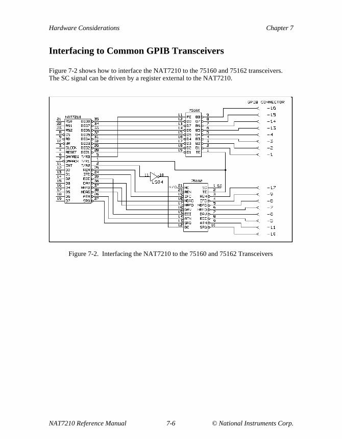
Hardware Considerations Chapter 7
NAT7210 Reference Manual 7-6 © National Instruments Corp.
Interfacing to Common GPIB Transceivers
Figure 7-2 shows how to interface the NAT7210 to the 75160 and 75162 transceivers.The SC signal can be driven by a register external to the NAT7210.
Figure 7-2. Interfacing the NAT7210 to the 75160 and 75162 Transceivers

© National Instruments Corp. A-1 NAT7210 Reference Manual
Appendix ACommon Questions
This appendix lists common questions and answers.
If there are two devices, one using a NAT7210 with a 16 MHz clock frequency, andanother using the NAT7210 with a 5 MHz clock frequency, will the one with thehigher clock frequency communicate faster?
Yes, but not much faster. Depending on the application, the 16 MHz chip might increasethroughput by up to 15%. It will not make your throughput 3 times faster.
When the NAT7210 sends a data byte, it delays for a time “T1.” The longer the T1 delayis, the longer it takes to transfer a byte.
For example, suppose you program the NAT7210 to use a T1 delay of 500 ns. For a 5MHz clock, T1 would have to be at least 600 ns, because it must be some multiple of theclock period. On average, the actual delay would be about 700 ns, because you must addabout 0.5 of a clock period for synchronizing delays. For a 16 MHz clock, 500 ns is anexact multiple of the clock period, so the average T1 delay would be close to 500 ns + 0.5clock periods—about 531 ns.
Therefore, the T1 delay for a 16 MHz clock might be 169 ns shorter (on average) thanthat of a 5 MHz clock. The faster clock saves 169 ns of time on every bite. If yourthroughput is 10 kBytes/s, this will not be a noticeable time difference. However, if yourthroughput is 800 kBytes/s, the difference will be noticeable.
Although the faster clock frequencies don’t improve throughput very much, theNAT7210 is designed have high throughput at any clock frequency.
What should I do if I am using a clock that uses fractional output frequencies?
Simply round up to the next highest integer. Examples follow:
Fractional Output Frequency ICR Value1.2 23.35 4
3.6864 4
You can write any integer higher than the actual input frequency to the ICR. Even if youdo not write any value to the ICR, the NAT7210 will still work with actual frequencies of1.2, 3.35, 3.6864 MHz, because it defaults to 8 MHz.

Common Questions Appendix A
NAT7210 Reference Manual A-2 © National Instruments Corp.
The NAT7210 uses the input clock to generate certain delays, such as the T1 delay (seeprevious question). For example, suppose you program the NAT7210 to use a 2 µsnominal T1 delay. The NAT7210 examines the ICR register to determine how manyclock periods to wait. If the ICR contains 2, the NAT7210 assumes that the inputfrequency is 2 MHz and the clock period is 500 ns. For a delay of 2 µs, the NAT7210calculates that it will need to wait:
2 µs ÷ 500 ns = 4 clock periods
If the ICR contains 2, the NAT7210 waits for 4 clock periods regardless of the actualclock frequency. If the actual frequency is 1.2 MHz (with a clock period of 833 ns), theactual delay will be:
4 clock periods x 833 ns = 3.33 µs
3.33 µs is longer than the nominal 2 µs, but this is acceptable. The T1 delay can be longerthan 2 µs.

© National Instruments Corp. B-1 NAT7210 Reference Manual
Appendix BIntroduction to the GPIB
This appendix discusses the history of the GPIB, GPIB hardware configurations, andserial polling.
History of the GPIB
Hewlett-Packard developed the original GPIB (and called it the HP-IB) in the late 1960s.Hewlett-Packard developed its HB-IB to connect and control programmable instrumentsthat Hewlett-Packard had manufactured. The introduction of digital controllers andprogrammable test equipment created the need for a standard, high-speed interface thatwould permit communication between instruments and controllers from various vendors.In 1975, the IEEE published ANSI/IEEE Standard 488-1975, IEEE Standard DigitalInterface for Programmable Instrumentation, which contained the electrical, mechanical,and functional specifications of an interfacing system. The original IEEE 488-1975 wasrevised in 1978 primarily for editorial clarification and addendum. This bus is now usedworldwide and is known by three names:
• General Purpose Interface Bus (GPIB)
• Hewlett-Packard Interface Bus (HP-IB)
• IEEE 488 Bus
Because the original IEEE 488 document contained no guidelines for preferred syntaxand format conventions, work continued on the specification to enhance systemcompatibility and configurability among test systems. This work resulted in asupplement standard—IEEE 488.2, Codes, Formats, Protocols, and CommonCommands—that you use with IEEE 488 (which was renamed IEEE 488.1).
IEEE 488.2 does not replace IEEE 488.1. Many devices still conform only toIEEE 488.1. IEEE 488.2 builds on IEEE 488.1 by defining a minimum set of deviceinterface capabilities, a common set of data codes and formats, a device messageprotocol, a generic set of commonly needed device commands, and a new status reportingmodel.
In 1990, a consortium of test and measurement companies developed the StandardCommands for Programmable Instrumentation (SCPI) document. SCPI defines specificcommands that each instrument class (which usually includes instruments from variousvendors) must obey. Thus, SCPI guarantees complete system compatibility andconfigurability among these instruments. You no longer need to learn a differentcommand set for each instrument, and you can easily replace an instrument from onevendor with an instrument from another.

Introduction to the GPIB Appendix B
NAT7210 Reference Manual B-2 © National Instruments Corp.
The IEEE 488.1 Specification
The GPIB is a digital, 8-bit, parallel communications interface with maximum datatransfer rates over 1 MB/s. The bus supports one system controller—usually acomputer—and up to 14 additional instruments. Because the GPIB is an 8-bit parallelinterface with fast data transfer rates, it has gained popularity in other applications suchas intercomputer communication and peripheral control.
IEEE 488.2 and SCPI Specifications
Although IEEE 488.1 eliminated the need to find the right type of connector anddetermine which signal line was connected to which pin, it did not solve other problems.More than 10 years after the release of IEEE 488.1, IEEE 488.2 and SCPI solved theseproblems.
Problems with IEEE 488.1 Compatible Devices
Users of IEEE 488.1 compatible devices encountered the following problems:
• No common method for performing operations existed: In a system with twodifferent meters, one meter could require a command to take a reading while theother could take a reading without a command.
• No common data format existed among communicating devices: Twocommunicating devices used two different formats to represent the same number.
• No common command set existed: Two devices performed identical functions, butused completely different device-dependent data messages.
• Status reporting was unique to each device: Each device reported its statusinformation in a different format.
The IEEE 488.2 Solution
The IEEE 488.2 standard eliminates the IEEE 488.1 problems through the followingsolutions:
• IEEE 488.2 contains a minimum set of required device interface capabilities.
• IEEE 488.2 specifies a way of presenting data through data formats and codes.
• IEEE 488.2 defines a specific protocol for sending device messages and the syntaxfor multiple commands in a single string.

Appendix B Introduction to the GPIB
© National Instruments Corp. B-3 NAT7210 Reference Manual
• IEEE 488.2 contains a common command set.
• IEEE 488.2 contains a standard status reporting model.
SCPI Specification
The SCPI specification expands the IEEE 488.2 common command set by defining asingle, comprehensive command set that is suitable for all instruments. For example, allSCPI-compatible voltmeters, regardless of manufacturer or model, respond to the samecommand for reading AC voltage. Their response format is also the same.
SCPI embraces many of the commands and protocols that the hardware-independentportion of the IEEE 488.2 standard defines. Figure B-1 illustrates the structure of theGPIB standards.
SCPI CommandHierarchy
Standard ResponseFormat
Standard ProgramCommand Set
Software/Firmware
Hardware
IEEE 4
88.2
IEEE 4
88.1
Common CommandsSyntax/Data Structures
Handshaking/ControlMechanical/Electrical Standards
Figure B-1. Structure of the GPIB Standards

Introduction to the GPIB Appendix B
NAT7210 Reference Manual B-4 © National Instruments Corp.
The combination of IEEE 488.2 and SCPI leads to greater productivity by featuringsoftware command standards and instant interchangeability. Rather than learning adifferent command set for each instrument, you can focus on solving measurementproblems.
Although you can mix SCPI and non-SCPI instruments in a system, your completesystem must adhere to IEEE 488.2 for you to fully benefit from these standards.
See Appendix C, Standard Commands for Programmable Instruments (SCPI), for moreinformation.
GPIB Hardware Configuration
A GPIB hardware setup consists of two or more GPIB devices (instruments and/orinterface boards) that are connected by a GPIB cable. The cable assembly consists of ashielded 24-conductor cable with a plug and a receptacle (male/female) connector at eachend. With this design, you can link devices in a linear configuration, a star configuration,or a combination of these two configurations (see Figures B-2 and B-3).

Appendix B Introduction to the GPIB
© National Instruments Corp. B-5 NAT7210 Reference Manual
Device A
Device B
Device C
Figure B-2. Linear Configuration
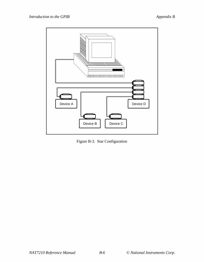
Introduction to the GPIB Appendix B
NAT7210 Reference Manual B-6 © National Instruments Corp.
Device A
Device B Device C
Device D
Figure B-3. Star Configuration

Appendix B Introduction to the GPIB
© National Instruments Corp. B-7 NAT7210 Reference Manual
GPIB Signals and Lines
The GPIB has 16 signal lines and 8 ground return or shield drain lines (see Figure B-4).All GPIB devices share the same 24 bus lines. The 16 signal lines fall into three groups:
• Eight data lines.
• Five interface management lines.
• Three handshake lines.
DIO1DIO2DIO3DIO4
EOIDAV
NRFDNDAC
IFCSRQATN
SHIELD
DIO5DIO6DIO7DIO8RENGND (TW PAIR W/DAV) GND (TW PAIR W/NRFD) GND (TW PAIR W/NDAC) GND (TW PAIR W/IFC) GND (TW PAIR W/SRQ) GND (TW PAIR W/ATN) SIGNAL GROUND
123456789
101112
131415161718192021222324
Figure B-4. GPIB Connector and Pin Assignments
Data Lines
The eight data lines, DIO1 through DIO8, carry the command and data messages on theGPIB. All commands and most data use the 7-bit ASCII or ISO code set; thus, the eighthbit, DIO8, is not used or is used for parity.

Introduction to the GPIB Appendix B
NAT7210 Reference Manual B-8 © National Instruments Corp.
Interface Management Lines
The following lines manage the flow of information across the GPIB:
• Interface Clear (IFC)
• Attention (ATN)
• Remote Enable (REN)
• End-or-Identify (EOI)
• Service Request (SRQ)
Interface Clear (IFC)
Only the System Controller can control the IFC line. The System Controller uses IFC totake control of the bus asynchronously. This action must initially be done to establishController status.
The IFC line is the master reset of the GPIB. When it is asserted, all devices return to aknown quiescent state.
Interface Clear(IFC)
• Places all devices into quiescent state.
• Is asserted by System Controller.
– 300.0005 V

Appendix B Introduction to the GPIB
© National Instruments Corp. B-9 NAT7210 Reference Manual
Attention (ATN)
When the ATN line is asserted, all devices become Listeners and participate in thecommunication. ATN signifies that a GPIB command message or data message ispresent on the data lines. When ATN is unasserted, information on the bus is interpretedas a data message. When ATN is asserted, information on the bus is interpreted as acommand message.
Attention(ATN)
• Notifies devices of current data type.
• Is asserted by Controller-In-Charge.
– 300.0005 V
Controller
Talker Listener(s)
AllDevices
ATN asserted
Command messages
ATN unasserted
Data messages

Introduction to the GPIB Appendix B
NAT7210 Reference Manual B-10 © National Instruments Corp.
Remote Enable (REN)
The System Controller uses the REN line to put devices into a remote state. Each devicehas its own remote/local state capabilities. The IEEE 488 standard requires a device to gointo a remote programming state whenever the REN line is asserted and addressed tolisten.
Remote Enable(REN)
• Enables devices for remote programming.
• Is asserted by System Controller.
– 300.0005 V
End-or-Identify (EOI)
Some devices terminate their output data by using the EOI line. A Talker asserts EOIalong with the last byte of data. A Listener stops reading data when the EOI is asserted.More details of transfer termination are presented later. This line is also used in parallelpolling, which will be discussed later.
End Or Identify(EOI)
• Signals end of data.
• Signals the execution of a Parallel Poll.
• Is asserted by current Talker.
– 300.0005 V

Appendix B Introduction to the GPIB
© National Instruments Corp. B-11 NAT7210 Reference Manual
Service Request (SRQ)
A device asserts the SRQ line at any time in order to notify the CIC that it needs service.The SRQ line remains asserted until the device is serial polled. The Controller mustmonitor SRQ, poll the device, and determine the type of service the device needs.
Service Request(SRQ)
• Alerts Controller that service is needed.
• Is asserted by Non-Controller.
– 300.0005 V
Handshake Lines
Three lines asynchronously control the transfer of message bytes among devices:
• Not Ready For Data (NRFD)
• Not Data Accepted (NDAC)
• Data Valid (DAV)
The GPIB uses a three-wire interlocking handshake scheme. This handshake schemeguarantees that message bytes on the data lines are sent and received withouttransmission error.
Not Ready For Data (NRFD)
The NRFD line indicates whether a device is ready to receive a data byte. When aController is sending commands, all devices drive NRFD. When a Talker is sending datamessages, only Listeners drive NRFD.
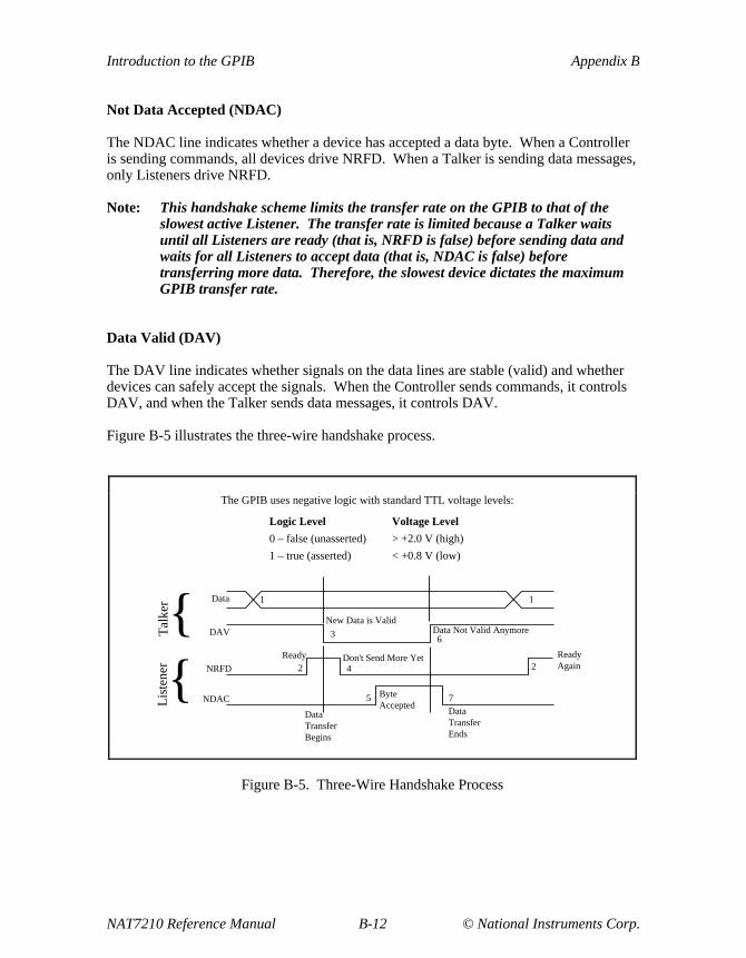
Introduction to the GPIB Appendix B
NAT7210 Reference Manual B-12 © National Instruments Corp.
Not Data Accepted (NDAC)
The NDAC line indicates whether a device has accepted a data byte. When a Controlleris sending commands, all devices drive NRFD. When a Talker is sending data messages,only Listeners drive NRFD.
Note: This handshake scheme limits the transfer rate on the GPIB to that of theslowest active Listener. The transfer rate is limited because a Talker waitsuntil all Listeners are ready (that is, NRFD is false) before sending data andwaits for all Listeners to accept data (that is, NDAC is false) beforetransferring more data. Therefore, the slowest device dictates the maximumGPIB transfer rate.
Data Valid (DAV)
The DAV line indicates whether signals on the data lines are stable (valid) and whetherdevices can safely accept the signals. When the Controller sends commands, it controlsDAV, and when the Talker sends data messages, it controls DAV.
Figure B-5 illustrates the three-wire handshake process.
1Data 1
2
63
42
5 7
DAVNew Data is Valid
Don't Send More YetReady
NRFD
NDAC ByteAccepted
DataTransferBegins
DataTransferEnds
ReadyAgain
Data Not Valid Anymore
The GPIB uses negative logic with standard TTL voltage levels:
Logic Level
0 – false (unasserted)
1 – true (asserted)
Voltage Level
> +2.0 V (high)
< +0.8 V (low)
Tal
ker{
Lis
tene
r{
Figure B-5. Three-Wire Handshake Process
Appendix B Introduction to the GPIB
© National Instruments Corp. B-13 NAT7210 Reference Manual
Three-Wire Handshake Process
GPIB devices use the three-wire handshake process to transfer information. The three-wire handshake process is identical for command and data transfers. During commandtransfers, the Controller drives the DIO and DAV lines; all devices drive the NRFD andNDAC lines. During data transfers, the Talker drives the DIO and DAV lines; allListeners drive the NRFD and NDAC lines.
Devices drive the NDAC and NRFD lines with open-collector drivers, so if any devicedrives NDAC (or NRFD) to a low voltage level, the signal is logically asserted (true).If no device drives NDAC (or NRFD) to a low voltage level, the signal floats to a highvoltage level; thus, the signal is logically unasserted (false).
The following actions occur during the three-wire handshake process (refer toFigure B-5):
1. The Talker (or Controller) places data on the DIO lines and waits at least T1 seconds.
2. After the T1 delay, the Talker waits until the Listener unasserts NRFD. NRFDunasserted (not Not-Ready-For Data) indicates that the Listener can receive the databyte.
3. The Talker asserts DAV to indicate that new data is valid on the DIO lines.
4. The Listener asserts NRFD to signal a Not Ready Status (Don’t Send More Yet).
5. When the Listener accepts the current byte (by placing it in some internal buffer orby otherwise processing it), the Listener unasserts NDAC.
6. The Talker unasserts DAV.
7. The Listener asserts NDAC, then the Talker executes step 1 to begin transferring thenext byte.
Physical and Electrical Specifications
To achieve the GPIB’s high data transfer rate, you must limit the physical distancebetween devices and the number of devices on the bus. This limitation is necessarybecause the GPIB is a transmission line system. Any distance beyond the maximumallowable cable length, as well as any excess GPIB device loads, can surpass interfacecircuit drive capability.
The IEEE 488 standard dictates the following limits:
• The total length of all cables is less than or equal to 2 m times the number ofconnected devices—up to a total of 20 m.
Introduction to the GPIB Appendix B
NAT7210 Reference Manual B-14 © National Instruments Corp.
• No more than 15 devices are connected to each bus, with at least two-thirds of thedevices powered on.
If you must exceed these limits, you can purchase bus extenders and expanders.
Controllers, Talkers, and Listeners
All buses operate under rules that ensure that data passes reliably and that instruments donot use the bus simultaneously. To determine which device has active control of the bus,devices are categorized as Controllers, Talkers , or Listeners. Whenever two devicescommunicate, one device will be a Talker and the other will be a Listener. In addition,one device will always be a Controller.
Controllers
Most GPIB systems consist of one computer and a variety of instruments. In this type ofsystem, the computer is typically the System Controller. If multiple computers areconnected, several devices can have Controller capability, but only one Controller isactive, or Controller-In-Charge (CIC), at a time. Active control can pass from thecurrent CIC to an idle Controller.
For each GPIB system, you must define a System Controller. You usually define theSystem Controller through jumper settings on the GPIB interface board, a softwareconfiguration file, or both. Only one device on the bus, the System Controller, can makeitself the CIC.
The four primary responsibilities of a Controller are the following:
• Defining the communication links.
• Responding to devices requesting service.
• Sending GPIB commands.
• Passing/receiving control.

Appendix B Introduction to the GPIB
© National Instruments Corp. B-15 NAT7210 Reference Manual
Talkers and Listeners
You can set most GPIB devices to be either Talkers or Listeners. However, some devicesonly talk or only listen. Each device accepts its own command set and has its ownmethod of terminating data strings. Talkers and Listeners have the following properties:
• Talkers
– Are instructed by the Controller to talk.
– Place data on the GPIB.
– Permit only one device to talk at a time.
• Listeners
– Are instructed by the Controller to listen.
– Read data that the Talker places on the GPIB.
– Permit several devices to be Listeners simultaneously.
You can compare GPIB operation to a classroom. The instructor (Controller) controls thecommunication of data between the students (devices). The instructor decides who talksand who listens. On the GPIB, a device cannot talk or listen unless the Controllerexplicitly tells it to do so.
Figure B-6 shows a system setup example.
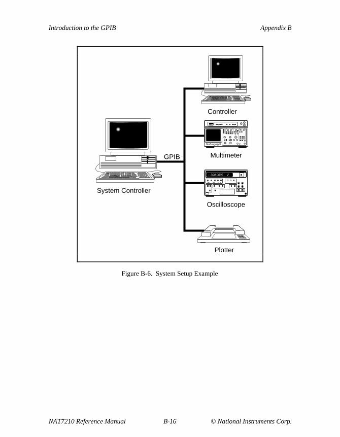
Introduction to the GPIB Appendix B
NAT7210 Reference Manual B-16 © National Instruments Corp.
– 300.0005 V
System Controller
Multimeter
Oscilloscope
Plotter
Controller
GPIB
Figure B-6. System Setup Example

Appendix B Introduction to the GPIB
© National Instruments Corp. B-17 NAT7210 Reference Manual
Data and Command Messages
In a classroom, when the instructor tells the students who is the Talker and who are theListeners, his or her information is a command—not the actual data information that theinstructor will send. On the GPIB, this distinction is not so intuitive. The busmanagement line, ATN, determines what type of message you are sending on the bus. Ifthis line is unasserted, the information on the bus is a data message; if this line isasserted, the information is a command message from the Controller to all devices. Thedevices on the GPIB monitor the ATN line, determine the data type, and treat the dataappropriately.
GPIB Addressing Protocol
In a classroom, an instructor either speaks to the entire class or to a particular student. Tospeak to a student, the instructor first addresses that student by name.
Addressing on the GPIB follows the same idea. Before any communication can takeplace on the bus, you must address the Talker and Listener. Before any data passesbetween devices, the Controller determines who talks and who listens.
In the classroom, we address people by their names. However, on the GPIB, each device(including the Controller) has a unique primary GPIB address in the range of 0 to 30(decimal). The Controller places a command message specifying the addresses of theTalker and Listener devices on the bus.
The Controller sends a single byte (8 bits) of information for a Talker or Listener addresscommand message. Address command messages have the following format:
7 46 5 3 2 1 0
XLATA XXXX
Bit
Data
Bits 0 through 4 contain the binary GPIB primary address of the device incommunication, and either bit 5—Listener Address (LA)—or bit 6—Talker Address(TA)—will be set if the device is a Talker or a Listener. Bit 7 is never used and isconsidered a don’t care bit. For simplicity, assume bit 7 is zero.

Introduction to the GPIB Appendix B
NAT7210 Reference Manual B-18 © National Instruments Corp.
Consider an example in which a Controller at primary GPIB address 0 talks to a device atprimary GPIB address 1. To establish the communication link, the Controller must sendits GPIB talk address and the device’s listen address over the GPIB. In this example,these addresses are as follows:
Bit Patterns Sent to Set Up Talker
Bit pattern:
00000
ADRTA
010
01000000
Talker's GPIB Address is 0
Hexadecimal value:
4
0100
0
0000
Hex 40 = ASCII "@"
Refer to the Multiline Interface Command Messages table (in Appendix C) and find thehex 40 location. On the same row under the Msg column, you see the message MTA0,which means My Talk Address 0. Hex 40 is the command message for setting device 0 tobe a Talker.
Bit Patterns Sent to Set Up Listener
Bit pattern:
00001
ADRLA
001
00100001
Listener's GPIB Address is 1
Hexadecimal value:
2
0010
1
0001
Hex 21 = ASCII "!"
Refer to the Multiline Interface Command Messages table and find the hex 21 location.On the same row under the Msg column, you see the message MLA1, which means MyListen Address 1 . Hex 21 is the command message for setting device 1 to be a Listener.

Appendix B Introduction to the GPIB
© National Instruments Corp. B-19 NAT7210 Reference Manual
Reading the Multiline Interface Command Messages Table
By using the Multiline Interface Command Messages table, you can understand how theGPIB circuitry interprets the bit patterns to produce the proper message commands. TheMultiline Interface Command Messages table is organized into four groups of columns.The left or first group of columns (hex 00–1F) represents the primary GPIB addresses.Moving to the right to the next group of columns (hex 20–3F), you will find thecorresponding listen addresses (MLA). The listen address of a device is formed byadding hex 20 to the GPIB primary address. Again, move right to the next group ofcolumns (hex 40–5F) for the corresponding talk addresses (MTA). You form the talkaddress of a device by adding hex 40 to the GPIB primary address.
Secondary Addressing
A device can have a secondary address. A secondary address is in the range of 0 to 30decimal (IE hex). To form a secondary address command (bit pattern), add 96 decimal(60 hex) to the secondary address. You address a device with a secondary address bysending the primary GPIB address, then the corresponding secondary address. Withsecondary addressing, you can assign up to 961 talk and listen addresses. Mostinstruments do not use secondary addressing. In the Multiline Interface CommandMessages table, the group of columns on the right (hex 60–7F) represents the secondaryGPIB address commands.
Unaddressing Command Messages
The CIC uses two special command messages to clear the bus of Talkers and Listenersbefore assigning new Talkers and Listeners. These command messages are Untalk andUnlisten. The Untalk (UNT) command (hex 5F (ASCII “_”)) unaddresses the currentTalker. The Untalk command is merely a command for convenience, because addressingone Talker automatically unaddresses all others. The Unlisten (UNL) command (hex 3F(ASCII “?”)) unaddresses all current Listeners on the bus. You cannot unaddress only asingle Listener if you have previously addressed several Listeners. You must use theUNL command to guarantee that you address only desired Listeners.
Termination Methods
When devices send data over the GPIB, they use up to three different methods to signifythe end of a data transfer. These methods are EOS, EOI, and the count method.
Termination methods in GPIB are necessary only for data messages, not for commandmessages.

Introduction to the GPIB Appendix B
NAT7210 Reference Manual B-20 © National Instruments Corp.
EOS Method
The EOS method uses an EOS character, which signifies the termination of data thatdevices send on the GPIB. This EOS character can be any character. However, it iscommonly a carriage return (hex 0D) or a line feed (hex 0A) that the Talker places as thelast character in a data string. The Listener reads individual data bytes from the Talkeruntil the Listener reads the EOS character. When the Listener reads the EOS character, itknows that there is no more data, so it completes the read operation.
You must configure the Talker and Listener to use the EOS method before thecommunication takes place. Many devices send specific EOS characters and look forspecific characters from other devices, so it is important for you to read thedocumentation for all devices to see which termination method the devices use.
To use the EOS method in a classroom setting, the instructor and students would use acertain word to finish all communication within the classroom. As with the GPIB, theinstructor and students would define this method and the word used before anycommunication took place. In the GPIB and in the classroom, the termination signal issent by using the normal data path (data lines in GPIB, or speech in the classroom).
EOI Method
The EOI method uses the GPIB EOI line, which is separate from the eight data lines onthe GPIB. In the EOI method, when the Talker sends the last byte of data in thetransmission, it sets the EOI line high to specify that the byte is the last byte to be sent.The Listener monitors the EOI line and recognizes when there is no more data. You mustestablish ahead of time whether the Talker will use the EOI method, so you can correctlyconfigure the Listener to watch the EOI line.
Students could use the EOI method in the classroom: they would wave device cards inthe air to signal when they have finished speaking. This form of communication isseparate from the method of sending data (speech), but the other Listeners can monitorthis communication while they receive data (hear the speech).
Count Method
The count method uses neither the EOI line nor the EOS character. In the count method,the device that receives information specifies the number of bytes to read. Through thismethod, a listening device reads a specified amount of data and prevents the talkingdevice from sending more data. If you do not clear the remaining data from the bus, youcan recover it later.
Students can use the count method in the classroom. Students count the words ofsomeone who is talking. The Listener announces that he or she will listen to only a
Appendix B Introduction to the GPIB
© National Instruments Corp. B-21 NAT7210 Reference Manual
specified number of words. Beyond this number of words, the Listener will not hear anyfurther information from the Talker. If the Listener wants more information, he or sherequests more words from the Talker.
Combinations of Termination Methods
You can use any combination of the three termination methods to terminatecommunication on the GPIB. For example, you can specify an EOS character and alsouse the EOI line method. In this case, when the end of the string is reached, the devicesending the data will send an EOS character and assert the EOI line. When you use morethan one method, the first termination method recognized causes the termination. In thisexample, the EOS character or EOI line causes termination, depending on which methodthe device recognizes first.
In general, when you use more than one termination method at a time, all methods arelogically ORed together for a result. Therefore, if you use all three methods, thecommunication termination will take place if the device sees the EOS character, thesystem asserts the EOI line, or the count value has been reached.
Serial Polling
Servicing SRQs
In the classroom, an instructor is in charge of the class and controls activity. The GPIBworks in a similar fashion: the Controller bus controls when tasks are performed. In theclassroom, a student must have permission to speak, and on the GPIB, no device cancommunicate unless it is addressed to talk on the bus. A device may, however, need tocommunicate with the Controller before the Controller tells it to talk. In a classroom,students who have something to say usually raise their hands. On the GPIB, any devicecan assert the SRQ line, which is separate from the data lines. SRQ informs theController that a device needs attention. The next section discusses how the SRQ line isasserted and how the device that asserts it is identified.
Serial Polling Devices
This section investigates how the GPIB handles the SRQ line. Remember the SRQ linepurpose: signaling to the Controller that a device needs attention. When SRQ is asserted,it is the responsibility of the Controller to determine who requested service by checkingall devices individually. Checking the devices individually is known as polling thedevices. The Controller can poll devices in two ways: in serial or in parallel. Thisappendix discusses serial polling and parallel polling.
Serial polling obtains specific information from a device. When you serial poll, theController sends a special command message—Serial Poll Enable (SPE)—to the device,

Introduction to the GPIB Appendix B
NAT7210 Reference Manual B-22 © National Instruments Corp.
directing it to return its serial poll status byte. The SPE message sets the IEEE 488.1serial poll mode in the device, so when the device is addressed to talk, it returns a single8-bit status byte. This serial poll status byte is different for each type of instrument;except for one bit, you must refer to the instrument user manual for information on theother bits. Bit 6 (hex 40) of any serial poll status byte indicates whether a devicerequested service by asserting the SRQ line. The device uses the other seven bits of thestatus byte to specify why it needs attention.
After the Controller reads the status byte, it sends another command message, Serial PollDisable (SPD), to the device. The SPD message terminates the serial poll mode, thusreturning the device to its normal Talker/Listener state. Once a device requesting serviceis serial polled, it usually unasserts the SRQ line.
When a serial poll is conducted, the following sequence of events occurs:
System Controller GPIB Device
UNListen (UNL)
Device Listen Address
Serial Poll Enable (SPE)
Device Talk Address
Read (IBRD) Serial PollByte from Device
Serial Poll Disable (SPD)
UNTalk (UNT) All Devices
Turns off Serial Poll Mode
Serial Poll Byte Returned
Device Set as Talker
Generates Serial Poll Byte
Device as Listener
Figure B-7. Events During a Serial Poll
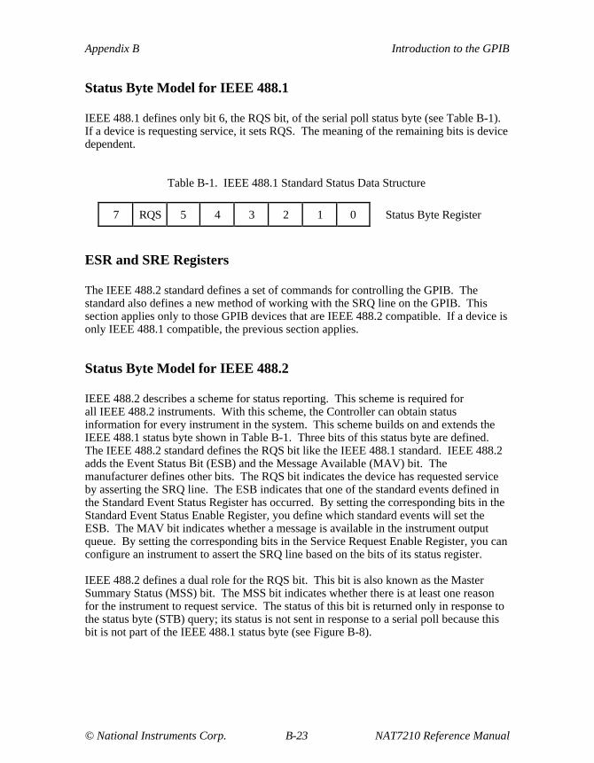
Appendix B Introduction to the GPIB
© National Instruments Corp. B-23 NAT7210 Reference Manual
Status Byte Model for IEEE 488.1
IEEE 488.1 defines only bit 6, the RQS bit, of the serial poll status byte (see Table B-1).If a device is requesting service, it sets RQS. The meaning of the remaining bits is devicedependent.
Table B-1. IEEE 488.1 Standard Status Data Structure
7 RQS 5 4 3 2 1 0 Status Byte Register
ESR and SRE Registers
The IEEE 488.2 standard defines a set of commands for controlling the GPIB. Thestandard also defines a new method of working with the SRQ line on the GPIB. Thissection applies only to those GPIB devices that are IEEE 488.2 compatible. If a device isonly IEEE 488.1 compatible, the previous section applies.
Status Byte Model for IEEE 488.2
IEEE 488.2 describes a scheme for status reporting. This scheme is required forall IEEE 488.2 instruments. With this scheme, the Controller can obtain statusinformation for every instrument in the system. This scheme builds on and extends theIEEE 488.1 status byte shown in Table B-1. Three bits of this status byte are defined.The IEEE 488.2 standard defines the RQS bit like the IEEE 488.1 standard. IEEE 488.2adds the Event Status Bit (ESB) and the Message Available (MAV) bit. Themanufacturer defines other bits. The RQS bit indicates the device has requested serviceby asserting the SRQ line. The ESB indicates that one of the standard events defined inthe Standard Event Status Register has occurred. By setting the corresponding bits in theStandard Event Status Enable Register, you define which standard events will set theESB. The MAV bit indicates whether a message is available in the instrument outputqueue. By setting the corresponding bits in the Service Request Enable Register, you canconfigure an instrument to assert the SRQ line based on the bits of its status register.
IEEE 488.2 defines a dual role for the RQS bit. This bit is also known as the MasterSummary Status (MSS) bit. The MSS bit indicates whether there is at least one reasonfor the instrument to request service. The status of this bit is returned only in response tothe status byte (STB) query; its status is not sent in response to a serial poll because thisbit is not part of the IEEE 488.1 status byte (see Figure B-8).

Introduction to the GPIB Appendix B
NAT7210 Reference Manual B-24 © National Instruments Corp.
Use
r R
eque
st
Com
man
d E
rror
Exe
cutio
n E
rror
Dev
ice
Dep
ende
nt E
rror
Que
ry E
rror
Req
uest
Con
trol
Ope
ratio
n C
ompl
ete
7 6 5 4 3 2 1 0Standard
Event Status Register*ESR?
7 6 5 4 3 2 1 0
&&
&&
&&
&&
StandardEvent Status Enable
Register*ESE <NRf >
*ESE?
7 ESB MAV 3 2 1 0
7 5 4 3 2 1 0
&
&&
&&
&&
Output Queue
RQS
MSS6
ServiceRequest
Generation
QueueNot-Empty
Pow
er O
n
Logi
cal O
R
Service RequestEnable Register
*SRE <NRf >*SRE?
read by Serial Poll
read by *STB?
Status Byte Register
Logi
cal O
R
Figure B-8. IEEE 488.2 Standard Status Structures
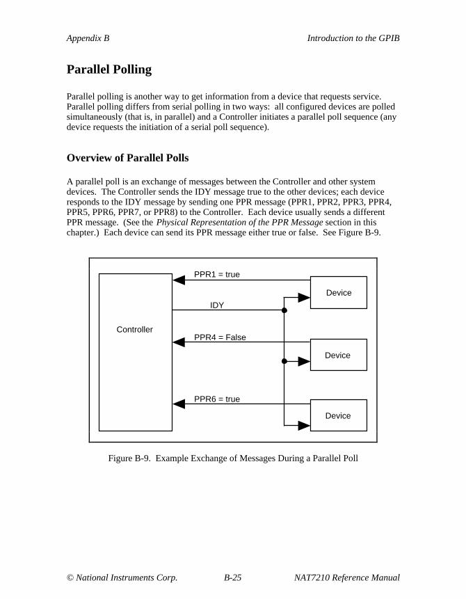
Appendix B Introduction to the GPIB
© National Instruments Corp. B-25 NAT7210 Reference Manual
Parallel Polling
Parallel polling is another way to get information from a device that requests service.Parallel polling differs from serial polling in two ways: all configured devices are polledsimultaneously (that is, in parallel) and a Controller initiates a parallel poll sequence (anydevice requests the initiation of a serial poll sequence).
Overview of Parallel Polls
A parallel poll is an exchange of messages between the Controller and other systemdevices. The Controller sends the IDY message true to the other devices; each deviceresponds to the IDY message by sending one PPR message (PPR1, PPR2, PPR3, PPR4,PPR5, PPR6, PPR7, or PPR8) to the Controller. Each device usually sends a differentPPR message. (See the Physical Representation of the PPR Message section in thischapter.) Each device can send its PPR message either true or false. See Figure B-9.
Controller
PPR1 = true
PPR4 = False
PPR6 = true
IDY
Device
Device
Device
Figure B-9. Example Exchange of Messages During a Parallel Poll

Introduction to the GPIB Appendix B
NAT7210 Reference Manual B-26 © National Instruments Corp.
Determining the Value of the PPR Message
Each device examines its local ist message and its Sense bit (S) to determine whether itwill send its PPR message true or false. Table B-2 illustrates how the ist message and theSense bit affect the value of the PPR message.
Table B-2. PPR Message Value
ist Message Sense Bit (S) PPR Message Sent
0 (False) 0 True
0 (False) 1 False
1 (True) 0 False
1 (True) 1 True
The ist message usually reflects a bit of status information about the device. Forexample, when the device has taken a measurement, it can assert its local ist message.The Sense bit is part of the configuration of a device. Each device has an independentSense bit.
The meaning of the PPR message and the local ist message is device dependent.
Configuring a Device for Parallel Polls
To configure a device to respond to parallel polls, you must supply the device with twopieces of data:
• The PPR message that the device should send to the Controller (PPR1, PPR2, . . , orPPR8)
• The value of the Sense bit of the device.
You can configure devices locally or remotely. You locally configure (Parallel Pollfunction subset PP2) a device by setting knobs or switches on the front panel of thedevice (or by physically manipulating the device in some other way). You remotelyconfigure (Parallel Poll function subset PP1) a device by sending messages across theGPIB from the Controller to the device. If a device has not been configured to respond toparallel polls, it does not respond to parallel polls.
Some devices support only local configuration and some support only remoteconfiguration. Some devices do not support any parallel polls (Parallel Poll functionsubset PP0).

Appendix B Introduction to the GPIB
© National Instruments Corp. B-27 NAT7210 Reference Manual
Determining the PPE Message
The PPE message contains the parallel poll configuration data for a device. Table B-3shows how you determine the value of DIO[7:1] for the PPE message. As with allcommands, the DIO[8] is a don’t care bit.
Table B-3. Determining the PPE Message
Sense Bit (S) PPR Messageto Send
PPE Message(hex)
0000
0000
PPR1PPR2PPR3PPR4
PPR5PPR6PPR7PPR8
60616263
64656667
1111
1111
PPR1PPR2PPR3PPR4
PPR5PPR6PPR7PPR8
68696A6B
6C6D6E6F
Physical Representation of the PPR Message
To send a PPR message true, a device drives the corresponding GPIB DIO signal lowwith an open-collector driver. For example, to send the PPR4 message true, a devicedrives the GPIB DIO4 signal low.
Because devices drive the DIO signals with open-collector drivers during parallel polls,more than one device can share a PPR message. If a Controller detects a PPR messagebeing sent true, the Controller knows that one or more of the devices sharing the PPRmessage is sending the PPR message true.

Introduction to the GPIB Appendix B
NAT7210 Reference Manual B-28 © National Instruments Corp.
Clearing and Triggering Devices
A Controller can clear devices in several ways. It can assert the IFC line to clear alldevices, or it can send the Device Clear (DCL) command message to clear all devices onthe bus. To clear a single device, a Controller can address the device to listen, then sendthe Selected Device Clear (SDC) command message.
After a device receives DCL or SDC, its clear state is device dependent. Generally,sending DCL or SDC is a less extreme method of clearing a device than asserting IFC.Most devices support the DCL and SDC method; all devices support the IFC method.
All devices in multidevice measurement systems must often be sampled as closelytogether as possible. You can trigger devices simultaneously by using the Group ExecuteTrigger (GET) command message. This command message causes all devices that havetriggering capability and that are currently addressed to initiate a preprogrammed action.The action could be, for example, to take a measurement or begin a sweep.

© National Instruments Corp. C-1 NAT7210 Reference Manual
Appendix CStandard Commands for ProgrammableInstruments (SCPI)
This appendix discusses the Standard Commands for Programmable Instruments (SCPI)document, the required SCPI commands, and SCPI programming.
GPIB instrumentation standards have progressed from the IEEE 488.1 standard to theIEEE 488.2 standard to SCPI. The IEEE 488.1 standard simplified and standardized theinterconnection of programmable instrumentation by defining the electrical, mechanical,and protocol specifications of the GPIB. Before IEEE 488.1, each manufacturer had itsown proprietary interface.
The IEEE 488.2 standard kept the IEEE 488.1 standard intact, but it made systems morecompatible and program development easier by defining standard data codes and formats,a status-reporting model, a message exchange protocol, a set of common commands forall instruments, and Controller requirements. Because the IEEE 488.1 standard did notaddress these issues, manufacturers implemented each item differently, thus creatingcomplex programming and unpredictable development costs.
SCPI uses the IEEE 488.2 standard as a basis for defining a single, comprehensivecommand set that is suitable for all instruments. SCPI users no longer need to learn adifferent command set for each instrument in their systems.
You can use IEEE 488.1, IEEE 488.2, and SCPI instruments and Controllers together, butyou achieve the maximum benefits with a system consisting of an IEEE 488.2 Controllerand SCPI instruments.

SCPI Appendix C
NAT7210 Reference Manual C-2 © National Instruments Corp.
IEEE 488.2 Common Commands Required by SCPI
All SCPI devices require the mandatory common commands that the IEEE 488.2standard defines (see Table C-1). This command set consists of program commands andstatus queries that are common to all devices. These commands and queries do nothandle device-specific operations; they handle more general operations such as deviceidentification, operation synchronization, standard event status enabling and reporting,device reset and self-test, and service request enable reporting.
Table C-1. IEEE 488.2 Common Commands Required by SCPI
Command Description
*CLS Clear Status Command
*ESE Standard Event Status Enable Command
*ESE? Standard Event Status Enable Query
*ESR? Standard Event Status Register Query
*IDN? Identification Query
*OPC Operation Complete Command
*OPC? Operation Complete Query
*RST Reset Command
*SRE Service Request Enable Command
*SRE? Service Request Enable Query
*STB? Read Status Byte Query
*TST? Self-Test Query
*WAI? Wait-to-Continue Command

Appendix C SCPI
© National Instruments Corp. C-3 NAT7210 Reference Manual
SCPI Required Commands
In addition to the IEEE 488.2 common commands and queries, SCPI defines its own setof required common commands (see Table C-2). In general, these commands build onthe IEEE 488.2 common command set, but SCPI expands the standard status-reportingmodel defined in IEEE 488.2 with OPERation and QUEStionable status registers. Forboth of these registers, commands read the contents of the EVENt and CONDitionregisters, set the ENABle mask, and read the ENABle mask.
The SYSTem command set defines functions that are not related to instrumentperformance, such as commands for performing general housekeeping like settingTIME or SECurity. The subcommand query ERRor? requests the next entry from theerror/event queue of the device. The PRESet command configures the SCPI anddevice-dependent status registers to be reported through the SCPI status-reporting model.
Table C-2. SCPI Required Commands
Command Description
:SYSTem :ERRor?
Collects functions not related to instrument performanceRequests the next entry from the instrument’s error queue
:STATus :OPERation [:EVENt]? :CONDition? :ENABle :QUEStionable [:EVENt]? :CONDition :ENABle :ENABle? :PRESet
Controls the SCPI-defined status-reporting structuresSelects the Operation structureReturns the contents of the Event registerReturns the contents of the Condition registerReads the Enable maskSelects the Questionable structureReturns the contents of the Event registerReturns the contents of the Condition registerSets the Enable mask, which allows event reportingReads Enable maskEnables all required event reporting
SCPI Optional Commands
The SCPI command set that an instrument uses can include a subset of the commandscovered in the SCPI specification. An instrument designed to measure voltage does notimplement commands to measure frequency. An instrument can also support specialcommands not presently covered in the SCPI standard.
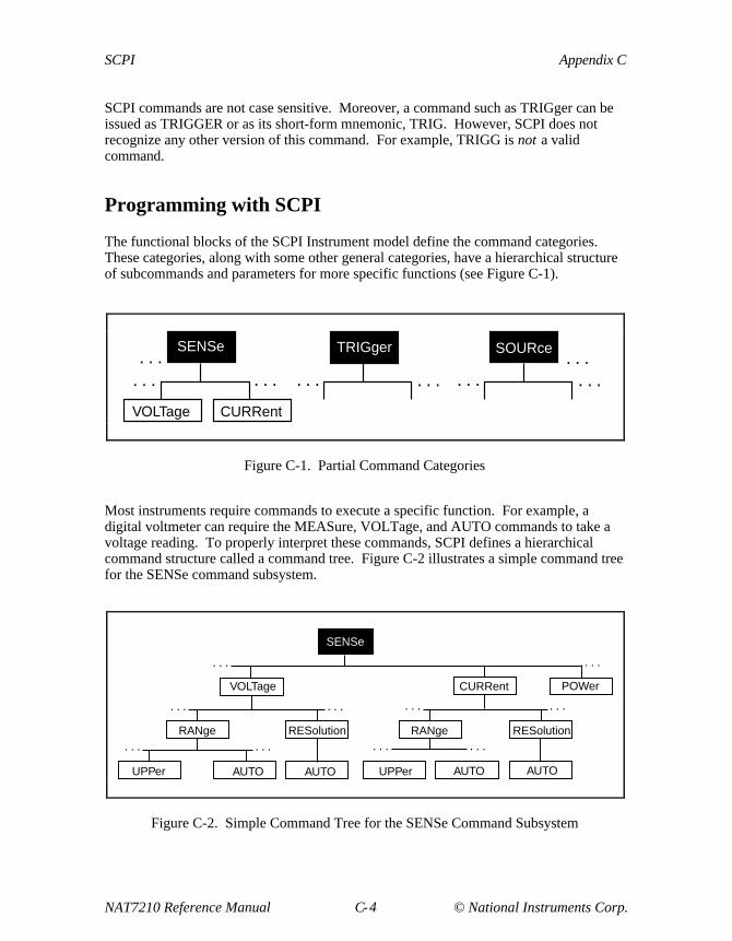
SCPI Appendix C
NAT7210 Reference Manual C-4 © National Instruments Corp.
SCPI commands are not case sensitive. Moreover, a command such as TRIGger can beissued as TRIGGER or as its short-form mnemonic, TRIG. However, SCPI does notrecognize any other version of this command. For example, TRIGG is not a validcommand.
Programming with SCPI
The functional blocks of the SCPI Instrument model define the command categories.These categories, along with some other general categories, have a hierarchical structureof subcommands and parameters for more specific functions (see Figure C-1).
. . .. . .
. . . . . .. . . . . .. . .
SENSe TRIGger SOURce
VOLTage CURRent
. . .
Figure C-1. Partial Command Categories
Most instruments require commands to execute a specific function. For example, adigital voltmeter can require the MEASure, VOLTage, and AUTO commands to take avoltage reading. To properly interpret these commands, SCPI defines a hierarchicalcommand structure called a command tree. Figure C-2 illustrates a simple command treefor the SENSe command subsystem.
. . .
. . .
. . .
. . .. . .
SENSe
RANge RESolution
. . .
VOLTage
UPPer AUTO AUTO
. . .. . .
. . .. . .RANge RESolution
CURRent
UPPer AUTO AUTO
POWer
Figure C-2. Simple Command Tree for the SENSe Command Subsystem

Appendix C SCPI
© National Instruments Corp. C-5 NAT7210 Reference Manual
The SENSe commands control the characteristics of the conversion process for the inputsensors of the instrument. Examples include the following:
• Signal amplitude for VOLTage, CURRent, and POWer
• Filter BANDwidth
• FREQuency characteristics
The SENSe commands do not mathematically manipulate the data after it has beenconverted.
Constructing SCPI Commands by Using the Hierarchical CommandStructure
The SENSe commands program an instrument to control the conversion of the signal intointernal data that can be manipulated. SENSe commands control such parameters asrange, resolution, gate time, and normal mode rejection. By using the partial commandtree shown in Figure C-3, you can construct the short form command to configure aninstrument for a voltage measurement that uses dynamic autoranging. This command isas follows:
SENS:VOLT:RANG:AUTO:DIR:EITH
. . .
. . .
. . .
. . .. . .
SENSe
RANGe
. . .
VOLTage
UPPer AUTO
. . .
.
.
. . .DIRection
CURRent
UP DOWN EITHer
POWer
LOWer
.
.
Figure C-3. Partial Command Tree for the SENSe Command Subsystem

SCPI Appendix C
NAT7210 Reference Manual C-6 © National Instruments Corp.
The SOURce commands program the instrument to generate a signal based on specifiedcharacteristics and internal data. SOURce block functions specify such signal parametersas amplitude modulation, power, current, voltage, and frequency. By using the partialcommand tree shown in Figure C-4, you can construct the short form command to set theupper limit of the current output to 500 mA. This command is as follows:
SOUR:CURR:LIM:HIGH 0.5
. . .
. . .
. . .
SOURce
LIMit
. . .
VOLTage
AMPLitude HIGH
.
.
CURRent POWer
OFFSet
.
.
LOW STATe
Figure C-4. Partial Command Tree for the SOURce Command Subsystem
The TRIGger commands program the instrument to synchronize its operation based onsome event. Trigger sources include an internal event or condition involving theinstrument functionality, an external condition such as an analog or digital signal, or asoftware command. By using the partial command tree shown in Figure C-5, you canconstruct the short form command to trigger an instrument from an external source. Thiscommand is as follows:
TRIG:SOUR:EXT
. . .
TRIGger
. . .
HOLD
SOURce
EXTernalBUS INTernal LINKLINEIMMediateECLTrg
Figure C-5. Partial Command Tree for the TRIGger Command Subsystem

Appendix C SCPI
© National Instruments Corp. C-7 NAT7210 Reference Manual
Parsing SCPI Commands
Colons separate each command and instruct the instrument parser to move down a levelin the command tree hierarchy. In situations where two commands are issued withoutchanging levels, a semicolon separates the commands. Commas separate parameterssuch as numeric, extended numeric, discrete, and Boolean. Commas are generallyignored with two exceptions:
• Spaces should not break command words.
• Spaces must not separate commands and parameters.
The colon preceding the first command in a SCPI message instructs the parser in theSCPI instrument to reset itself to the root level in the hierarchy.
Unless specifically noted, all commands have a query form as defined in the IEEE 488.2standard. When a query command is received, the current instrument settings associatedwith that command are placed in the instrument output buffer. For more commands,consult the SCPI standard or the user manuals for the SCPI instruments of interest in aparticular application.
© National Instruments Corp. D-1 NAT7210 Reference Manual
Appendix DMultiline Interface Command Messages
This appendix lists the multiline interface messages and describes the mnemonics andmessages that correspond to the interface functions. The multiline interface messages areIEEE 488 defined commands that are sent and received with ATN TRUE. The interfacefunctions include initializing the bus, addressing and unaddressing devices, and settingdevice modes for local or remote programming.

Multiline Interface Command Messages Appendix D
NAT7210 Reference Manual D-2 © National Instruments Corp.
Multiline Interface Messages
Hex Oct Dec ASCII Msg Hex Oct Dec ASCII Msg
00 000 0 NUL 20 040 32 SP MLA001 001 1 SOH GTL 21 041 33 ! MLA102 002 2 STX 22 042 34 " MLA203 003 3 ETX 23 043 35 # MLA304 004 4 EOT SDC 24 044 36 $ MLA405 005 5 ENQ PPC 25 045 37 % MLA506 006 6 ACK 26 046 38 & MLA607 007 7 BEL 27 047 39 ' MLA7
08 010 8 BS GET 28 050 40 ( MLA809 011 9 HT TCT 29 051 41 ) MLA90A 012 10 LF 2A 052 42 * MLA100B 013 11 VT 2B 053 43 + MLA110C 014 12 FF 2C 054 44 , MLA120D 015 13 CR 2D 055 45 - MLA130E 016 14 SO 2E 056 46 . MLA140F 017 15 SI 2F 057 47 / MLA15
10 020 16 DLE 30 060 48 0 MLA1611 021 17 DC1 LLO 31 061 49 1 MLA1712 022 18 DC2 32 062 50 2 MLA1813 023 19 DC3 33 063 51 3 MLA1914 024 20 DC4 DCL 34 064 52 4 MLA2015 025 21 NAK PPU 35 065 53 5 MLA2116 026 22 SYN 36 066 54 6 MLA2217 027 23 ETB 37 067 55 7 MLA23
18 030 24 CAN SPE 38 070 56 8 MLA2419 031 25 EM SPD 39 071 57 9 MLA251A 032 26 SUB 3A 072 58 : MLA261B 033 27 ESC 3B 073 59 ; MLA271C 034 28 FS 3C 074 60 < MLA281D 035 29 GS 3D 075 61 = MLA291E 036 30 RS 3E 076 62 > MLA301F 037 31 US 3F 077 63 ? UNL
Message Definitions
DCL Device Clear MSA My Secondary AddressGET Group Execute Trigger MTA My Talk AddressGTL Go To Local PPC Parallel Poll ConfigureLLO Local Lockout PPD Parallel Poll DisableMLA My Listen Address

Appendix D Multiline Interface Command Messages
© National Instruments Corp. D-3 NAT7210 Reference Manual
Multiline Interface Messages
Hex Oct Dec ASCII Msg Hex Oct Dec ASCII Msg
40 100 64 @ MTA0 60 140 96 ` MSA0,PPE41 101 65 A MTA1 61 141 97 a MSA1,PPE42 102 66 B MTA2 62 142 98 b MSA2,PPE43 103 67 C MTA3 63 143 99 c MSA3,PPE44 104 68 D MTA4 64 144 100 d MSA4,PPE45 105 69 E MTA5 65 145 101 e MSA5,PPE46 106 70 F MTA6 66 146 102 f MSA6,PPE47 107 71 G MTA7 67 147 103 g MSA7,PPE
48 110 72 H MTA8 68 150 104 h MSA8,PPE49 111 73 I MTA9 69 151 105 i MSA9,PPE4A 112 74 J MTA10 6A 152 106 j MSA10,PPE4B 113 75 K MTA11 6B 153 107 k MSA11,PPE4C 114 76 L MTA12 6C 154 108 l MSA12,PPE4D 115 77 M MTA13 6D 155 109 m MSA13,PPE4E 116 78 N MTA14 6E 156 110 n MSA14,PPE4F 117 79 O MTA15 6F 157 111 o MSA15,PPE
50 120 80 P MTA16 70 160 112 p MSA16,PPD51 121 81 Q MTA17 71 161 113 q MSA17,PPD52 122 82 R MTA18 72 162 114 r MSA18,PPD53 123 83 S MTA19 73 163 115 s MSA19,PPD54 124 84 T MTA20 74 164 116 t MSA20,PPD55 125 85 U MTA21 75 165 117 u MSA21,PPD56 126 86 V MTA22 76 166 118 v MSA22,PPD57 127 87 W MTA23 77 167 119 w MSA23,PPD
58 130 88 X MTA24 78 170 120 x MSA24,PPD59 131 89 Y MTA25 79 171 121 y MSA25,PPD5A 132 90 Z MTA26 7A 172 122 z MSA26,PPD5B 133 91 [ MTA27 7B 173 123 { MSA27,PPD5C 134 92 \ MTA28 7C 174 124 | MSA28,PPD5D 135 93 ] MTA29 7D 175 125 } MSA29,PPD5E 136 94 ^ MTA30 7E 176 126 ~ MSA30,PPD5F 137 95 _ UNT 7F 177 127 DEL
Message Definitions
PPE Parallel Poll Enable SPE Serial Poll EnablePPU Parallel Poll Unconfigure TCT Take ControlSDC Selected Device Clear UNL UnlistenSPD Serial Poll Disable UNT Untalk

© National Instruments Corp. E-1 NAT7210 Reference Manual
Appendix EMnemonics Key
This appendix defines the mnemonics (abbreviations) that this manual uses for functions,remote messages, local messages, states, bits, registers, integrated circuits, and systemfunctions.
The mnemonic types in this key are abbreviated to mean the following:
A Auxiliary or Accessory CommandsB BitF FunctionIC Integrated CircuitLM Local MessageP Physical Device PinR RegisterRM Remote MessageSF System FunctionST State

Mnemonics Key Appendix E
NAT7210 Reference Manual E-2 © National Instruments Corp.
Mnemonic Type Definition
A
ACCRA R Accessory Register AACCRB R Accessory Register BACCRE R Accessory Register EACCRF R Accessory Register FACCRI R Accessory Register IACCRJ R Accessory Register JACCR R Accessory RegisterACCWR R Accessory Write RegisterACDS ST Acceptor Data State (AH function)ACG RM Addressed Command GroupACRDY B Acceptor Ready State bitACRS ST Acceptor Ready StateAD[5–1] B NAT7210 GPIB Address bits 5 through 1ADHS B Acceptor Data Holdoff State bitADMR R Address Mode RegisterADR R Address RegisterADR0 R Address Register 0ADR1 R Address Register 1ADSC B Address Status Change bitADSC IE B Address Status Change Interrupt Enable bitADSR R Address Status RegisterAEFN B FIFO A Empty Flag bitAEHS B Acceptor End Holdoff State bitAH F Acceptor Handshake functionAH1 F Acceptor HandshakeANHS1 B Acceptor Not Ready Holdoff bitANHS2 B Acceptor Not Ready Holdoff Immediately bitANRS ST Acceptor Not Ready StateAPT B Address Pass Through bitAPT IE B Address Pass Through Interrupt Enable bitARS B Address Register Select bitATCT B Automatic Take Control bitATN RM AttentionATN* B Attention bitATN IE B Attention Interrupt Enable bitATNI B ATN Interrupt bitATNI IE B ATN Interrupt Enable bitAUXCR R Auxiliary Command Register

Appendix E Mnemonics Key
© National Instruments Corp. E-3 NAT7210 Reference Manual
Mnemonic Type Definition
AUXMR R Auxiliary Mode RegisterAUXRA R Auxiliary Register AAUXRB R Auxiliary Register BAUXRE R Auxiliary Register EAUXRF R Auxiliary Register FAUXRG R Auxiliary Register GAUXRI R Auxiliary Register I
B
BCR R Bus Control RegisterBI B Byte In bitBI IE B Byte In Interrupt Enable bitBIN B Binary bitBO B Byte Out bitBO IE B Byte Out Interrupt Enable bitBSR R Bus Status Register
C
CDOR R Command/Data Out RegisterCHES B Clear Holdoff On End Select bitch_rst A Chip Reset auxiliary commandCIC B Controller-In-Charge bitCIC IE B Controller-In-Charge Interrupt Enable bitClear ERR A Clear ERR Interrupt auxiliary commandclrpi A Clear Page-In Registers auxiliary commandCMDR R Command RegisterCO B Command Out bitCO IE B Command Out Interrupt Enable bitcont Continuous modeCPT B Command Pass Through bitCPT ENABLE B Command Pass Through Enable bitCPT IE B Command Pass Through Interrupt Enable bitCPTR R Command Pass Through Register
Mnemonics Key Appendix E
NAT7210 Reference Manual E-4 © National Instruments Corp.
Mnemonic Type Definition
D
DAC RM Data Accepteddacr A Release DAC Holdoff auxiliary commanddai A Disable IMR2, IMR1, And IMR0 Interrupts auxiliary
commanddai B Disable IMR2, IMR1, And IMR0 Interrupts bitdal B Disable Listener bitdat B Disable Talker bitDAV RM Data ValidDAV B GPIB Data Valid Signal bitDCAS B Device Clear Active State bitDCAS IE B Device Clear Active State Interrupt Enable bitDCL RM Device ClearDEC B Device Clear bitDEC IE B Device Clear Interrupt Enable bitDET B Device Execute Trigger bitDET IE B Device Execute Trigger Interrupt Enable bitDHADC B DAC Holdoff On DCL Or SDC Command bitDHADT B DAC Holdoff On GET Command bitDHALA B DAC Holdoff On All Listener Addresses Command bitDHALL B DAC Holdoff On All UCG, ACG, And SCG Commands
bitDHATA B DAC Holdoff On All Talker Addresses Command bitDHDC B DAC Holdoff On DCAS Command bitDHDT B DAC Holdoff On DTAS Command bitDHUNTL B DAC Holdoff On The UNL Or UNT Command bitDI B Data In bitDI IE B Data In Interrupt Enable bitDIO P GPIB Data Input/Output pinsDIR R Data In RegisterDISTCT B Disable Automatic Take Control bitDL B Disable Listener bitDL0 B Disable Listener 0 bitDL1 B Disable Listener 1 bitDMAE B DMA Enable bitDMAEN B DMA Enable bitDMAI B DMA Input Enable bitDMAO B DMA Output Enable bitDO B Data Out bitDO IE B Data Out Interrupt Enable bitDRQ B DMA Request Pin Status bitDT B Disable Talker bitDT F Device Trigger functionDT0 B Disable Talker 0 bit

Appendix E Mnemonics Key
© National Instruments Corp. E-5 NAT7210 Reference Manual
Mnemonic Type Definition
DT1 B Disable Talker 1 bitDTAS ST Device Trigger Active State
E
edpa B Enable Dual Primary Addressing Mode bitEND B End Received bitEND IE B End Received Interrupt Enable bitEND RX B End Received bitEOI RM End or IdentifyEOI B End-or-Identify bitEOIOE B GPIB EOI Signal Output Enable bitEOS RM End of StringEOS0 B End-of-String bit 0EOS1 B End-of-String bit 1EOS2 B End-of-String bit 2EOS3 B End-of-String bit 3EOS4 B End-of-String bit 4EOS5 B End-of-String bit 5EOS6 B End-of-String bit 6EOS7 B End-of-String bit 7EOSR R End-of-String RegisterERR B Error bitERR IE B Error Interrupt Enable bitESB B Event Status BitEXTDAC External DAC
F
F[3–0] Clock Frequencyfeoi A Send EOI With The Next Bytefget A Force Group Execute Trigger auxiliary command
G
GET B Group Execute Trigger bitGET IE B Group Execute Trigger Interrupt Enable bitGLINT B Global Interrupt Enable bitgts A Go To Standby auxiliary command

Mnemonics Key Appendix E
NAT7210 Reference Manual E-6 © National Instruments Corp.
Mnemonic Type Definition
H
hdfa A Holdoff On All Data auxiliary commandhdfe A Holdoff On End Only auxiliary commandhlda RFD Holdoff On All Data modeHLDA B Holdoff On All Data bithlde Holdoff On All END modehlde A Holdoff On All END Mode auxiliary commandHLDE B Holdoff On End bithldi A Holdoff Handshake Immediately auxiliary commandHSTS ST High-Speed T1 State
I
ICR R Internal Count RegisterICR2 R Internal Count Register 2IDY RM IdentifyIFC RM Interface ClearIFC IE B Interface Clear Interrupt Enable bitIFCI B IFC Interrupt bitIFCI IE B IFC Interrupt Enable bitIMR0 R Interrupt Mask Register 0IMR1 R Interrupt Mask Register 1IMR2 R Interrupt Mask Register 2INT B Interrupt Request Pin bitINT0 B Interrupt Register 0 Interrupt bitINV B Invert bitINT1 B Interrupt Register 1 Interrupt bitISR0 R Interrupt Status Register 0ISR1 R Interrupt Status Register 1ISR2 R Interrupt Status Register 2ISS B Individual Status Select bitist A Parallel Poll Flag auxiliary command
L
L F ListenLA B Listener Active bitLACS ST Listener Active StateLADCS ST Listener Addressed Or Active StateLADS ST Listener Addressed State (L function)LIDS ST Listener Idle StateLLO B Local Lockout bitLLOC B Local Lockout Change bit

Appendix E Mnemonics Key
© National Instruments Corp. E-7 NAT7210 Reference Manual
Mnemonic Type Definition
LLOC IE B Local Lockout Change Interrupt Enable bitLOCS ST Local StateLOK B Lockout bitLOKC B Lockout Change bitLOKC IE B Lockout Change Interrupt Enable bitlon B Listen-Only bitlon LM Listen OnlyLPAS B Listener Primary Addressed State bitLPAS ST Listener Primary Addressed StateLPIS ST Listener Primary Idle Stateltn A Listen auxiliary commandlul A Unlisten auxiliary commandlun LM Local Unlistenlut A Local Untalk auxiliary commandLWC B Listen When Controller bit
M
MA B My Address bitMA IE B My Address Interrupt Enable bitMAC B My Address Change bitMAC IE B My Address Change Interrupt Enable bitMAV B Message Available bitMICR R Modify Internal Count RegisterMICR B Modify Internal Count Register bitMJMN B Major-Minor bitMLA RM My Listen AddressMSA RM My Secondary AddressMSS B Master Summary Status bitMTA RM My Talk AddressMAT6 RM My Talk Address 6
N
nba B New Byte Available local message bitnba LM New Byte Availablenbaf A New Byte Available False auxiliary commandnbaf B New Byte Available False bitNDAC B Not Data Accepted bitNL B New Line Receive bitNL IE B New Line Receive Interrupt Enable bitNLEN B New Line End Enable bitnonvalid A Nonvalid auxiliary command issuedNPRS ST Negative Poll Response State

Mnemonics Key Appendix E
NAT7210 Reference Manual E-8 © National Instruments Corp.
Mnemonic Type Definition
NRFD RM Not Ready For Data MessageNTNL B No Talking When No Listener bit
O
OSA RM Other Secondary Address
P
P1 B Parallel Poll Response bit 1P2 B Parallel Poll Response bit 2P3 B Parallel Poll Response bit 3PACS ST Parallel Poll Addressed To Configure statePCG RM Primary Command GroupPE Pull-Up EnablePEND B Pending bitpiaccr A Page-In Accessory Register auxiliary commandpibcr A Page-In Bus Control Register auxiliary commandpieosr A Page-In End-of-String Register auxiliary commandpiimr2 A Page-In Interrupt Mask Register 2 auxiliary commandpon LM Power OnPP1 B Parallel Poll bit 1PP2 B Parallel Poll bit 2PPC RM Parallel Poll ConfigurePPD RM Parallel Poll DisablePPE RM Parallel Poll EnablePPR R Parallel Poll RegisterPPR RM Parallel Poll ResponsePPU RM Parallel Poll Unconfigurepts A Pass Through Next Secondary auxiliary command
R
rdy LM Ready For Next MessageREM B Remote bitREMC B Remote Change bitREMC IE B Remote Change Interrupt Enable bitREN RM Remote EnableREOS B End On EOS Received bitreqf A Request rsv False auxiliary commandreqt A Request rsv True auxiliary commandRFD RM Ready For Data

Appendix E Mnemonics Key
© National Instruments Corp. E-9 NAT7210 Reference Manual
Mnemonic Type Definition
rhdf B Release RFD Holdoffrhdf A Release RFD Holdoff auxiliary commandRL1 F Remote/Localrlc B Release Control commandRLC B Remote/Local Change bitRLC IE B Remote/Local Change Interrupt Enable bitrpp A Clear/Set Request Parallel Pollrpp1 A Execute Parallel Poll auxiliary commandRPP2 B Request Parallel Poll 2 bitrqc B Request Control commandRQS RM Request Servicersv LM Request Servicersv B Request Service bitrsv2 A Request Service Bit 2 auxiliary commandrtl A Return To Local auxiliary command
S
S B Status Bit Polarity (Sense) bitS[6–1] B Serial Poll Status bits 6 through 1SASR R Source Acceptor Status RegisterSC P 75162 System Controller pinSCG RM Secondary Command GroupSDC RM Selected Device ClearSDHS Selected DAC Holdoffs Internal SignalSDYS ST Source Delay Stateseoi A Send EOI auxiliary commandSH F Source Handshake functionSH1A B Source Handshake State bit ASH1B B Source Handshake State bit BSHAS ST Source High-Speed Active Stateshdw A Clear/Set Shadow Handshake auxiliary commandsic A Clear/Set Send Interface Clear auxiliary commandSIDS ST Source Idle StateSISB B Static Interrupt Status bitSLOW B Slow Handshake LinesSPAS ST Serial Poll Active StateSPAS IE B Serial Poll Active State Interrupt Enable bitSPD RM Serial Poll DisableSPE RM Serial Poll EnableSPEOI B Send Serial Poll EOI bitSPIS ST Serial Poll Idle StateSPMR R Serial Poll Mode RegisterSPMS ST Serial Poll Mode StateSPMS B Serial Poll Mode State bitSPSR R Serial Poll Status Register
Mnemonics Key Appendix E
NAT7210 Reference Manual E-10 © National Instruments Corp.
Mnemonic Type Definition
SR1 F Service Request functionsre A Clear/Set Send Remote Enable auxiliary commandSRQ RM Service RequestSRQ IE B Service Request Interrupt Enable bitSRQI B Service Request bitSRQI IE B Service Request Interrupt Enable bitSRQS ST Service Request StateSTB RM Status ByteSTBO B Status Byte Out bitSTBO IE B Status Byte Out Interrupt Enable bitstdl A Set Short T1 Delay auxiliary commandSTRS ST Source Transfer Statesw7210 A Switch To Turbo+7210 Mode auxiliary commandswrst A Software Reset auxiliary command issuedSYNC B GPIB Synchronization bitSYNC IE B GPIB Synchronization Interrupt Enable bit
T
T F TalkerTA B Talker Active bitTACS ST Talker Active State (T function)TADS ST Talker Addressed Statetca A Take Control Asynchronously auxiliary commandtcs A Take Control Synchronously auxiliary commandtcse A Take Control Synchronously On End auxiliary commandTCT RM Take ControlTE F Extended TalkerTIDS ST Talker Idle Stateton LM Talk Onlyton B Talk-Only bitTPAS ST Talker Primary Addressed StateTPAS B Talker Primary Addressed State bitTPIS ST Talker Primary Idle StateTRI B Three-State Timing bitTRIG Triggertrig A Trigger auxiliary commandTRM0 B Transmit/Receive Mode bit 0TRM1 B Transmit/Receive Mode bit 1

Appendix E Mnemonics Key
© National Instruments Corp. E-11 NAT7210 Reference Manual
Mnemonic Type Definition
U
U B Unconfigure bitUCG RM Universal Command Groupulpa B Upper/Lower Primary Address bitUNC B Unrecognized Command bitUNC IE B Unrecognized Command Interrupt Enable bitunl A Unlisten auxiliary commandUNL RM Unlisten commandunt A Untalk auxiliary commandUNT RM Untalk commandUSTD B Ultra Short T1 Delay bit
V
valid A Valid auxiliary commandVSR R Version Status Registervstdl A Very Short T1 Delay auxiliary command
X
X B Don’t care bitXEOS B Transmit END With EOS bit

© National Instruments Corp. F-1 NAT7210 Reference Manual
Appendix FCustomer Communication
For your convenience, this appendix contains forms to help you gather the informationnecessary to help us solve technical problems you might have as well as a form you canuse to comment on the product documentation. Filling out a copy of the TechnicalSupport Form before contacting National Instruments helps us help you better and faster.
National Instruments provides comprehensive technical assistance around the world. Inthe U.S. and Canada, applications engineers are available Monday through Friday from8:00 a.m. to 6:00 p.m. (central time). In other countries, contact the nearest branch office.You may fax questions to us at any time.
Corporate Headquarters(512) 795-8248Technical support fax: (800) 328-2203
(512) 794-5678
Branch Offices Phone Number Fax NumberAustralia 03 9 879 9179 03 9 879 9422Austria 0662 45 79 90 19 0662 45 79 90 0Belgium 02 757 03 11 02 757 00 20Denmark 45 76 71 11 45 76 26 00Finland 90 502 2930 90 527 2321France 1 48 14 24 14 1 48 14 24 24Germany 089 714 60 35 089 741 31 30Hong Kong 2686 8505 2645 3186Italy 02 48301915 02 48301892Japan 03 5472 2977 03 5472 2970Korea 02 596 7455 02 596 7456Mexico 5 202 2544 5 520 3282Netherlands 03480 30673 03480 33466Norway 32 84 86 00 32 84 84 00Singapore 2265887 2265886Spain 91 640 0533 91 640 0085Sweden 08 730 43 70 08 730 49 70Switzerland 056 20 51 55 056 20 51 51Taiwan 02 737 4644 02 377 1200U.K. 01635 523154 01635 523545

Technical Support Form
Technical support is available at any time by fax. Include the information from yourconfiguration form. Use additional pages if necessary.
Name
Company
Address
Fax ( ) Phone ( )
Computer brand
Model Processor
Operating system
Speed MHz RAM MB
Display adapter
Mouse yes no
Other adapters installed
Hard disk capacity MB Brand
Instruments used
National Instruments hardware product(s)
Revision
Configuration
(continues)

The problem is
List any error messages
The following steps will reproduce the problem

Documentation Comment Form
National Instruments encourages you to comment on the documentation supplied withour products. This information helps us provide quality products to meet your needs.
Title: NAT7210TM Reference Manual
Edition Date: June 1995
Part Number: 370875A-01
Please comment on the completeness, clarity, and organization of the manual.
(continues)

If you find errors in the manual, please record the page numbers and describe the errors.
Thank you for your help.
Name
Title
Company
Address
Phone ( )
Mail to: Technical PublicationsNational Instruments Corporation6504 Bridge Point Parkway, MS 53-02Austin, TX 78730-5039
Fax to: Technical PublicationsNational Instruments CorporationMS 53-02(512) 794-5678
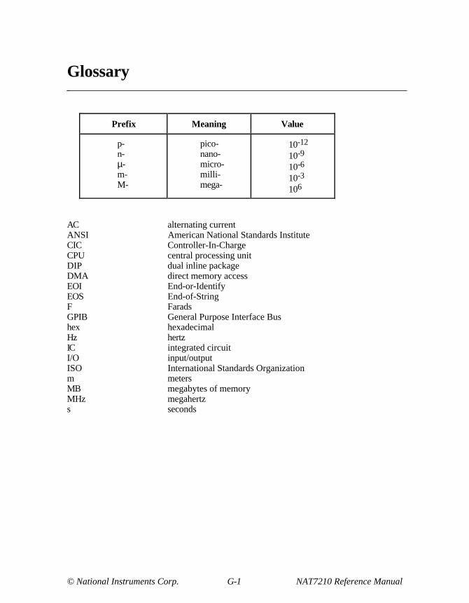
© National Instruments Corp. G-1 NAT7210 Reference Manual
Glossary
Prefix Meaning Value
p-n-µ-m-M-
pico-nano-micro-milli-mega-
10-12
10-9
10-6
10-3
106
AC alternating currentANSI American National Standards InstituteCIC Controller-In-ChargeCPU central processing unitDIP dual inline packageDMA direct memory accessEOI End-or-IdentifyEOS End-of-StringF FaradsGPIB General Purpose Interface Bushex hexadecimalHz hertzIC integrated circuitI/O input/outputISO International Standards Organizationm metersMB megabytes of memoryMHz megahertzs seconds

National Instruments Corp. I-1 NAT7210 Reference Manual
Index
Numbers
7210-mode interface registers, 3-1 to 3-64Address Mode Register (ADMR),
3-5 to 3-7Address Register (ADR), 3-8Address Register 0 (ADR0), 3-9Address Register 1 (ADR1), 3-10Address Status Register (ADSR),
3-11 to 3-13Auxiliary Mode Register (AUXMR),
3-14 to 3-26Auxiliary Register A (AUXRA),
3-27 to 3-28Auxiliary Register B (AUXRB), 3-29
to 3-30Auxiliary Register E (AUXRE), 3-31Auxiliary Register F (AUXRF), 3-32Auxiliary Register G (AUXRG),
3-33 to 3-34Auxiliary Register I (AUXRI), 3-35
to 3-36Bus Control Register (BCR)/Bus
Status Register (BSR), 3-37 to 3-38Command/Data Out Register
(CDOR), 3-39Command Pass Through Register
(CPTR), 3-40Data In Register (DIR), 3-41End-of-String Register (EOSR), 3-42hidden registers
address register map, 3-3auxiliary mode register map, 3-4
Internal Count Register (ICR), 3-43Internal Count Register 2
(ICR2), 3-44Interrupt Mask Register 0 (IMR0),
3-45 to 3-48
Interrupt Mask Register 1 (IMR1), 3-49 to 3-53
Interrupt Mask Register 2 (IMR2), 3-54 to 3-57
Interrupt Status Register 0 (ISR0), 3-45 to 3-48
Interrupt Status Register 1 (ISR1), 3-49 to 3-53
Interrupt Status Register 2 (ISR2), 3-54 to 3-57
Page-In state, 3-3Parallel Poll Register (PPR), 3-58
to 3-59register map, 3-2Serial Poll Mode Register (SPMR),
3-62 to 3-63Serial Poll Status Register (SPSR),
3-62 to 3-63Source/Acceptor Status Register
(SASR), 3-60 to 3-61Version Status Register (VSR), 3-64
9914-mode interface registers, 4-1 to 4-50Accessory Register A (ACCRA), 4-5Accessory Register B (ACCRB), 4-6
to 4-7Accessory Register E (ACCRE), 4-8Accessory Register F (ACCRF), 4-9Accessory Register I (ACCRI), 4-10Address Register (ADR), 4-11Address Status Register (ADSR),
4-12 to 4-14Auxiliary Command Register
(AUXCR), 4-15 to 4-27Bus Control Register (BCR)/Bus
Status Register (BSR), 4-28 to 4-29Command/Data Out Register
(CDOR), 4-30
Index
NAT7210 Reference Manual I-2
National Instruments Corp.
Command Pass Through Register (CPTR), 4-31
Data In Register (DIR), 4-32End-of-String Register (EOSR), 4-33hidden registers, 4-3Internal Count Register (ICR), 4-34Interrupt Mask Register 0 (IMR0),
4-35 to 4-38Interrupt Mask Register 1 (IMR1),
4-39 to 4-43Interrupt Mask Register 2 (IMR2),
4-44 to 4-47Interrupt Status Register 0 (ISR0),
4-35 to 4-38Interrupt Status Register 1 (ISR1),
4-39 to 4-43Interrupt Status Register 2 (ISR2),
4-44 to 4-47page-in condition, 4-3Parallel Poll Register (PPR), 4-48register map, 4-2Serial Poll Mode Register (SPMR),
4-49 to 4-50Serial Poll Status Register (SPSR),
4-49 to 4-50
A
A[5-1] bit, Address Register (ADR), 4-11acceptor handshake holdoffs
GPIB rdy message and RFD holdoffschoosing data-receiving
mode, 5-14data-receiving modes, 5-13
to 5-14generating rdy message, 5-13immediate RFD holdoff, 5-13
Accessory Register (ACCR) offset (table), 4-3
Accessory Register A (ACCRA), 4-5Accessory Register B (ACCRB), 4-6
to 4-7Accessory Register E (ACCRE), 4-8Accessory Register F (ACCRF), 4-9Accessory Register I (ACCRI), 4-10ACRDY bit, Source/Acceptor Status
Register (SASR), 3-60Active Controller State
changing states, 6-3 to 6-4definition, 6-3
AD[5-0 -- 1-0] bits, Address Register 0 (ADR0), 3-9
AD[5-1 -- 1-1] bits, Address Register 1 (ADR1), 3-10
AD[5-1] bits, Address Register (ADR), 3-8
Address Mode Register (ADMR), 3-5 to 3-7
Extended Dual Addressing mode, 3-6
Extended Single Addressing mode, 3-5
Listen Only (lon) mode, 3-6No Addressing mode, 3-5Normal Dual Addressing mode, 3-5Talk Only (ton) mode, 3-6TRM[1-0] bits, 3-7
Address Register (ADR)7210 mode, 3-89914 mode, 4-11
Address Register 0 (ADR0), 3-9Address Register 1 (ADR1), 3-10Address Status Register (ADSR)
7210 mode, 3-11 to 3-139914 mode, 4-12 to 4-14

Index
National Instruments Corp. I-3 NAT7210 Reference Manual
addressing, GPIB
. See
GPIB addressing.ADHS bit, Source/Acceptor Status
Register (SASR), 3-60, 5-15ADMR (Address Mode Register)
. See
Address Mode Register (ADMR).
ADR (Address Register)7210 mode, 3-89914 mode, 4-11
ADR0 (Address Register 0), 3-3, 3-9ADR1 (Address Register 1), 3-3, 3-10ADSC bit, Interrupt Status Register 2
(ISR2), 3-57ADSC IE bit, Interrupt Mask Register 2
(IMR2), 3-57ADSR (Address Status Register)
7210 mode, 3-11 to 3-139914 mode, 4-12 to 4-14
AEHS bit, Source/Acceptor Status Register (SASR), 3-60
ANHS1 bit, Source/Acceptor Status Register (SASR), 3-60
ANHS2 bit, Source/Acceptor Status Register (SASR), 3-60, 5-13
ANSI/IEEE standard
. See
IEEE 488.1 standard.APT bit, Interrupt Status
Register 1 (ISR1)7210 mode, 3-50 to 3-519914 mode, 4-41 to 4-42implementing logical devices, 5-5
APT IE bit, Interrupt Mask Register 1 (IMR1)
7210 mode, 3-50 to 3-519914 mode, 4-41 to 4-42
ARS bit, Address Register (ADR), 3-8ATCT bit, Accessory Register B
(ACCRB), 4-7
ATN bitAddress Status Register
(ADSR), 4-12Bus Control Register (BCR)/Bus
Status Register (BSR), 3-37, 4-28ATN* bit, Address Status Register
(ADSR), 3-11ATN (Attention) line, GPIB, B-9ATNI bit
Interrupt Status Register 0 (ISR0), 3-47
Interrupt Status Register 2 (ISR2), 4-46
ATNI IE bitInterrupt Mask Register 0
(IMR0), 3-47Interrupt Mask Register 2
(IMR2), 4-46Attention (ATN) line, GPIB, B-9Auxiliary Command Register (AUXCR),
4-15 to 4-27Chip Reset (ch_rst), 4-25Clear Disable IMR2, IMR1, and
IMR0 Interrupts (~dai), 4-22Clear Force Group Execute Trigger
(~fget), 4-19Clear Holdoff On All Data
(~hdfa), 4-18Clear Holdoff On END Only
(~hdfe), 4-19Clear Listen Only (~lon), 4-20Clear Page-In Registers (clrpi), 4-26Clear Parallel Poll Flag (~ist), 4-25Clear Request Parallel Poll
(~rpp), 4-21Clear Request Service bit 2
(~rsv2), 4-24Clear Return to Local (~rtl), 4-20

Index
NAT7210 Reference Manual I-4
National Instruments Corp.
Clear Send Interface Clear (~sic), 4-21, 6-1
Clear Send Remote Enable (~sre), 4-22, 6-2
Clear Shadow Handshaking (~shdw), 4-23
Clear Short T1 Delay (~stdl), 4-23Clear Software Reset (~swrst), 4-18Clear Talk Only (~ton), 4-20Clear Very Short T1 Delay
(~vstdl), 4-23Go To Standby (gts), 4-20, 6-4New Byte Available False
(nbaf), 4-19Page-In Accessory Register
(piaccr), 4-27Page-In Bus Register (pibcr), 4-26Page-In End-of-String Registers
(pieosr), 4-26Page-In Interrupt Mask Register 2
(piimr2), 4-25Pass Through Next Secondary
(pts), 4-23Release Control (rlc), 4-22Release DAC Holdoff
(nonvalid), 4-18Release DAC Holdoff (valid), 4-18Release RFD Holdoff (rhdf),
4-18, 5-11Request Control (rqc), 4-22Request rsv False (reqf), 4-24Request rsv True (reqt), 4-24, 5-16Send EOI With The Next Byte
(feoi), 4-20Set Disable IMR2, IMR1, and IMR0
Interrupts (dai), 4-22Set Force Group Execute Trigger
(fget), 4-19
Set Holdoff On All Data (hdfa), 4-18Set Holdoff On END Only
(hdfe), 4-19Set Listen Only (lon), 4-20Set Parallel Poll Flag (ist), 4-25Set Request Parallel Poll (rpp),
4-21, 6-7Set Request Service bit 2 (rsv2), 4-24Set Return to Local (rtl), 4-20Set Send Interface Clear (sic),
4-21, 6-1Set Send Remote Enable (sre),
4-21, 6-2Set Shadow Handshaking
(shdw), 4-23Set Short T1 Delay (stdl), 4-23Set Software Reset (swrst), 4-18Set Talk Only (ton), 4-20Set Very Short T1 Delay (vstdl), 4-23summary of commands (table), 4-15
to 4-17Switch To 7210 Mode (sw7210),
4-24, 5-1Take Control Asynchronously (tca),
4-21, 6-4Take Control Synchronously
(tcs), 4-21Auxiliary Mode Register (AUXMR),
3-14 to 3-26Chip Reset, 3-19Clear ADSC, 3-26Clear ATNI, 3-26Clear DEC, 3-25Clear DET, 3-25Clear END, 3-25Clear ERR, 3-25, 6-5Clear IFC (~sic & rsc), 3-22Clear IFCI, 3-26

Index
National Instruments Corp. I-5 NAT7210 Reference Manual
Clear LOKC, 3-26Clear Or Pulse Return To Local
(rtl), 3-20Clear Parallel Poll Flag (~ist), 3-18Clear REMC, 3-26Clear REN (~sre & rsc), 3-23Clear SRQI Command, 3-26Clear SYNC, 3-26Disable System Control (~rsc),
3-22, 6-2Execute Parallel Poll (rpp1), 3-24Finish Handshake (rhdf), 3-19Go To Standby (gts), 3-21Holdoff Handshake Immediately
(hldi), 3-25, 5-2, 5-13Immediate Execute Power-On
(pon), 3-18Listen (ltn), 3-22Listen In Continuous Mode
(ltn & cont), 3-24Local Unlisten (lun), 3-24New Byte Available False
(nbaf), 3-21Nonvalid Secondary Command Or
Address (nonvalid), 3-20Page-In Additional Registers
(page-in), 3-25register map, 3-4Release Control Command
(rlc), 3-20Request Control Command
(rqc), 3-20Request rsv False (reqf), 3-23Request rsv True (reqt), 3-23Send EOI (seoi), 3-20Set IFC (sic & rsc), 3-24Set Parallel Poll Flag (ist), 3-18Set REN (sre & rsc), 3-25
Set Return To Local (rtl), 3-20Set SYNC, 3-26summary of auxiliary commands
(table), 3-15 to 3-17Switch To 9914A Mode
(sw9914), 3-22Take Control Asynchronously
(tca), 3-21Take Control Synchronously
(tcs), 3-22Take Control Synchronously On
END (tcse), 3-23Trigger (trig), 3-19Unlisten (lul), 3-21Untalk (lut), 3-21Valid Secondary Command Or
Address (valid), 3-21writing to hidden registers, 3-14
Auxiliary Register A (AUXRA), 3-27 to 3-28
Auxiliary Register B (AUXRB), 3-29 to 3-30
Auxiliary Register E (AUXRE), 3-31Auxiliary Register F (AUXRF), 3-32Auxiliary Register G (AUXRG), 3-33
to 3-34Auxiliary Register I (AUXRI), 3-35
to 3-36
B
B2 bit, 5-10BCR (Bus Control Register)/BSR
(Bus Status Register)7210 mode, 3-37 to 3-389914 mode, 4-28 to 4-29
BI bit, Interrupt Status Register 0 (ISR0), 4-36

Index
NAT7210 Reference Manual I-6
National Instruments Corp.
BI IE bit, Interrupt Mask Register 0 (IMR0), 4-36
BIN bitAccessory Register A (ACCRA), 4-5Auxiliary Register A
(AUXRA), 3-27bits
A[5-1], 4-11ACRDY, 3-60AD[5-0 -- 1-0], 3-9AD[5-1], 3-8AD[5-1 -- 1-1], 3-10ADHS, 3-60, 5-15ADSC, 3-57ADSC IE, 3-57AEHS, 3-60ANHS1, 3-60ANHS2, 3-60, 5-13APT, 3-50 to 3-51, 4-41 to 4-42, 5-5APT IE, 3-50 to 3-51, 4-41 to 4-42ARS, 3-8ATCT, 4-7ATN, 3-37, 4-12, 4-28ATN*, 3-11ATNI, 3-47, 4-46ATNI IE, 3-47, 4-46B2, 5-10BI, 4-36BI IE, 4-36BIN, 3-27, 4-5BO, 4-36BO IE, 4-36CHES, 3-34CIC, 3-11, 4-47CIC IE, 4-47CO, 3-56, 6-4, 6-5CO IE, 3-56, 6-5CPT, 3-49 to 3-50, 5-6
CPT ENABLE, 3-30CPT IE, 3-49 to 3-50, 5-19CPT[7-0], 3-40, 4-31dal, 4-11dat, 4-11DAV, 3-37, 4-28DCAS, 4-42DCAS IE, 4-42DEC, 3-52, 5-19DEC IE, 3-52, 5-19DET, 3-51, 5-19DET IE, 3-51, 5-19DHADC, 3-31, 4-8, 5-19DHADT, 3-31, 4-8, 5-19DHALA, 3-32, 4-9, 5-6DHALL, 3-32, 4-9, 5-7DHATA, 3-32, 4-9, 5-6DHDC, 3-31, 5-19DHDT, 3-31, 5-19DHUNTL, 3-32, 4-9DI, 3-53, 5-11DI IE, 3-53, 5-11DIO[8-1], 3-39, 3-41, 4-30, 4-32DISTCT, 3-34DL, 3-8, 5-4DL0, 3-9DL1, 3-10DMAE, 4-10DMAI, 3-56, 4-36DMAO, 3-56, 4-35DO, 3-53, 5-8DO IE, 3-53, 5-8DT, 3-8, 5-4DT0, 3-9DT1, 3-10edpa, 4-11END, 4-37END IE, 3-51 to 3-52, 4-37
Index
National Instruments Corp. I-7 NAT7210 Reference Manual
END RX, 3-51 to 3-52, 5-11EOI, 3-10, 3-37, 4-27, 5-11EOS, 3-47, 4-45, 5-11EOS[7-0], 3-42, 4-33ERR, 3-52 to 3-53, 4-40, 5-8, 6-5ERR IE, 3-52 to 3-53, 4-40, 5-8, 6-5F(3-0), 3-43, 4-34GET, 4-39 to 4-40GET IE, 4-39 to 4-40GLINT, 3-45, 4-44HLDA, 3-28HLDE, 3-28IFC, 3-37, 4-27, 4-43IFC IE, 4-43IFCI, 3-47IFCI IE, 3-47INT, 3-54 to 3-55INT0, 4-35INT1, 4-36INV, 3-29, 4-6ISS, 3-29, 4-6LA, 3-12, 4-13, 5-4LLO, 4-12LLOC, 4-46LLOC IE, 4-46LOK, 3-56, 5-18LOKC, 3-57, 5-18LOKC IE, 3-57LPAS, 3-12, 4-12, 5-4LWC, 4-6MA, 4-42 to 4-43MA IE, 4-42 to 4-43MAC, 4-38MAC IE, 4-38MICR, 3-44MJMN, 3-13, 5-4, 5-5nba, 3-45, 3-60, 4-44NDAC, 3-37, 4-28
NL, 3-46, 4-45NLEN, 3-47, 4-46NRFD, 3-37, 4-28NTNL, 3-33 to 3-34, 5-7, 6-5P[3-1], 3-59PEND, 3-63, 4-49, 5-16PP1, 4-10PP2, 3-35, 5-17PP8-PP1, 4-48REM, 3-56, 4-12, 5-18REMC, 3-57, 5-18REMC IE, 3-57REN, 3-37, 4-27REOS, 3-27, 4-5RLC, 4-37 to 4-38RLC IE, 4-37 to 4-38RPP2, 3-34, 6-7rsv/RQS, 3-63, 4-50S, 3-59S[6-1], 3-62, 4-49S8, 3-62, 4-49SH1A, SH1B, 3-61SISB, 3-35 to 3-36SLOW, 3-44SPAS, 4-37SPAS IE, 4-37SPEOI, 3-30, 4-7SPMS, 3-11SRQ, 3-37, 4-28, 4-43SRQ IE, 4-43SRQI, 3-55SRQI IE, 3-55STBO, 3-46, 4-45STBO IE, 3-46, 4-45, 5-16SYNC, 3-48, 6-4SYNC IE, 3-48TA, 3-12 to 3-13, 4-13, 5-4TPAS, 3-12, 4-13, 5-4

Index
NAT7210 Reference Manual I-8
National Instruments Corp.
TRI, 3-29TRM[1-0], 3-7U, 3-58, 5-18ulpa, 4-14UNC, 4-40 to 4-41UNC IE, 4-40 to 4-41USTD, 3-35, 4-10, 5-2, 5-10V[3-0], 3-64X, 3-9, 3-64XEOS, 3-27, 4-5
BO bit, Interrupt Status Register 0 (ISR0), 4-36
BO IE bit, Interrupt Mask Register 0 (IMR0), 4-36
Bus Control Register (BCR)/Bus Status Register (BSR)
7210 mode, 3-37 to 3-389914 mode, 4-28 to 4-29
C
capabilities codes (table), 1-1 to 1-2CDOR (Command/Data Out Register)
7210 mode, 3-399914 mode, 4-30
CHES bit, Auxiliary Register G (AUXRG), 3-34
chip initialization sequenceasserting local pon message, 5-1clearing local pon message, 5-3configuring chip for GPIB
operation, 5-2enabling interrupts, 5-2placing NAT7210 in 7210 mode, 5-1setting clock frequency, 5-1
Chip Reset (chip_reset) command, Auxiliary Mode Register (AUXMR), 3-19
asserting local pon message, 5-1clearing RFD holdoff condition, 5-13
Chip Reset (ch_rst) command, Auxiliary Command Register (AUXCR), 4-26
CIC bitAddress Status Register
(ADSR), 3-11Interrupt Status Register 2
(ISR2), 4-47CIC IE bit, Interrupt Mask Register 2
(IMR2), 4-47CIC internal signal, 7-1 to 7-2Clear ADSC command, 3-26Clear ATNI command, 3-26Clear DEC command, 3-25Clear DET command, 3-25Clear Disable IMR2, IMR1, and IMR0
Interrupts (~dai) command, 4-22Clear END command, 3-25Clear ERR command, 3-25, 6-5Clear Force Group Execute Trigger
(~fget) command, 4-19Clear Holdoff On All Data (~hdfa)
command, 4-18Clear Holdoff On END Only (~hdfe)
command, 4-19Clear IFC (~sic & rsc) command, 3-22Clear IFCI command, 3-26Clear Listen Only (~lon) command, 4-20Clear LOKC command, 3-26Clear Or Pulse Return To Local (rtl)
command, 3-20Clear Page-In Registers (clrpi)
command, 4-26
Index
National Instruments Corp. I-9 NAT7210 Reference Manual
Clear Parallel Poll Flag (~ist) commandAuxiliary Command Register
(AUXCR), 4-25Auxiliary Mode Register
(AUXMR), 3-18Clear REMC command, 3-26Clear REN (~sre & rsc) command, 3-23Clear Request Parallel Poll (~rpp)
command, 4-21Clear Request Service bit 2 (~rsv2)
command, 4-24Clear Return to Local (~rtl)
command, 4-20Clear Send Interface Clear (~sic)
command, 4-21, 6-1Clear Send Remote Enable (~sre)
command, 4-22, 6-2Clear Shadow Handshaking (~shdw)
command, 4-23Clear Short T1 Delay (~stdl)
command, 4-23Clear Software Reset (~swrst)
command, 4-18Clear SRQI Command, 3-26Clear SYNC command, 3-26Clear Talk Only (~ton) command, 4-20Clear Very Short T1 Delay (~vstdl)
command, 4-23clearing devices, 5-19, B-28CLK signal
requirements, 7-5timing diagram, 7-5
clock frequency.
See also
Internal Count Register (ICR).
setting, 5-1difference between rates, A-1
clock frequency bits F(3-0), Internal Count Register (ICR), 3-43, 4-34
clrpi (Clear Page-In Registers) command, 4-26
CO bit, Interrupt Status Register 2 (ISR2), 3-56 to 3-57, 6-4, 6-5
CO IE bit, Interrupt Mask Register 2 (IMR2), 3-56 to 3-57, 6-5
Command/Data Out Register (CDOR)7210 mode, 3-399914 mode, 4-30
command messages, GPIB, B-17, B-19
. See also
GPIB messages.Command Pass Through Register
(CPTR)7210 mode, 3-409914 mode, 4-31
commands
. See
Auxiliary Command Register (AUXCR); Auxiliary Mode Register (AUXMR); Standard Commands for Programmable Instrumentation (SCPI).
continuous mode, 5-14controller software considerations
. See
GPIB Controller; System Controller.
count termination method, GPIB, B-20 to B-21
CPT bitimplementing logical devices, 5-6Interrupt Status Register 1 (ISR1),
3-49 to 3-50CPT ENABLE bit, Auxiliary Register B
(AUXRB), 3-30CPT IE bit, Interrupt Mask Register 1
(IMR1), 3-49 to 3-50, 5-19CPT[7-0] bits, Command Pass Through
Register (CPTR), 3-40, 4-31

Index
NAT7210 Reference Manual I-10
National Instruments Corp.
CPTR (Command Pass Through Register)7210 mode, 3-409914 mode, 4-31
CPU address bus, 7-3CPU data bus, 7-3CPU interface capabilities, 1-3CPU register control pins
CPU data bus, 7-3CS* and CPU address bus, 7-3RD*/WR* pins, 7-3
customer communication,
xv
, F-1
D
DAC holdoffdetermining occurrence of, 5-15purpose and use, 5-14 to 5-15
DACK* signal, 5-8, 5-12, 7-4~dai (Clear Disable IMR2, IMR1, and
IMR0 Interrupts) command, 4-22dai (Set Disable IMR2, IMR1, and IMR0
Interrupts) command, 4-22dal bit, Address Register (ADR), 4-11dat bit, Address Register (ADR), 4-11data bus pins, GPIB, 7-3Data In Register (DIR)
7210 mode, 3-419914 mode, 4-32
data lines, GPIB, B-7data messages, GPIB
. See
GPIB data messages.
data-receiving modes
. See
GPIB rdy message and RFD holdoffs.
Data Valid (DAV) line, GPIB, B-12DAV bit, Bus Control Register (BCR)/
Bus Status Register (BSR), 3-37, 4-28DCAS (Device Clear Active State), 5-19
DCAS bit, Interrupt Status Register 1 (ISR1), 4-42
DCAS IE bit, Interrupt Mask Register 1 (IMR1), 4-42
DCL (Device Clear) command, 5-19DEC bit, Interrupt Status Register 1
(ISR1), 3-52, 5-19DEC IE bit, Interrupt Mask Register 1
(IMR1), 3-52, 5-19DET bit, Interrupt Status Register 1
(ISR1), 3-51, 5-19DET IE bit, Interrupt Mask Register 1
(IMR1), 3-51, 5-19Device Clear Active State (DCAS), 5-19Device Clear (DCL) command, 5-19device status reporting (polling)
. See
parallel polling; serial polling.
Device Trigger Active State (DTAS), 5-19
devicesclearing, 5-19, B-28triggering, 5-19, B-28
DHADC bitAccessory Register E (ACCRE), 4-8Auxiliary Register E (AUXRE), 3-31device clearing, 5-19
DHADT bitAccessory Register E (ACCRE), 4-8Auxiliary Register E (AUXRE), 3-31device triggering, 5-19
DHALA bitAccessory Register F (ACCRF), 4-9Auxiliary Register F (AUXRF), 3-32implementing logical devices, 5-6
DHALL bitAccessory Register F (ACCRF), 4-9Auxiliary Register F (AUXRF), 3-32implementing logical devices, 5-7
Index
National Instruments Corp. I-11 NAT7210 Reference Manual
DHATA bitAccessory Register F (ACCRF), 4-9Auxiliary Register F (AUXRF), 3-32implementing logical devices, 5-6
DHDC bit, Auxiliary Register E (AUXRE), 3-31, 5-19
DHDT bit, Auxiliary Register E (AUXRE), 3-31, 5-19
DHUNTL bitAccessory Register F (ACCRF), 4-9Auxiliary Register F (AUXRF), 3-32
DI bit, Interrupt Status Register 1 (ISR1)description, 3-53receiving GPIB data messages, 5-11
DI IE bit, Interrupt Mask Register 1 (IMR1)
description, 3-53receiving GPIB data message, 5-11
DIO[8-1] bitsCommand/Data Out Register
(CDOR), 3-39, 4-30Data In Register (DIR), 3-41, 4-32
DIR (Data In Register)7210 mode, 3-419914 mode, 4-32
Disable System Control (~rsc) command, 3-22, 6-2
DISTCT bit, Auxiliary Register G (AUXRG), 3-34
DL bitAddress Register (ADR), 3-8implementing logical devices, 5-4
DL0 bit, Address Register 0 (ADR0), 3-9DL1 bit, Address Register 1
(ADR1), 3-10DMA
receiving GPIB data messages, 5-11sending GPIB data messages, 5-7
DMA pinsDACK*, 7-4DRQ, 7-3 to 7-4
DMAE bit, Accessory Register I (ACCRI), 4-10
DMAI bitInterrupt Mask Register 0
(IMR0), 4-36Interrupt Mask Register 2
(IMR2), 3-56DMAO bit
Interrupt Mask Register 0 (IMR0), 4-35
Interrupt Mask Register 2 (IMR2), 3-56
DO bit, Interrupt Status Register 1 (ISR1)description, 3-53sending GPIB data messages, 5-8
DO IE bit, Interrupt Mask Register 1 (IMR1)
description, 3-53sending GPIB data messages, 5-8
documentationconventions used in manual,
xiv
mnemonics key, E-1 to E-11organization of manual,
xiii
-
xiv
related documentation,
xiv-xv
DRQ signal, 7-3 to 7-4DT bit
Address Register (ADR), 3-8implementing logical devices, 5-4
DT0 bit, Address Register 0 (ADR0), 3-9DT1 bit, Address Register 1
(ADR1), 3-10DTAS (Device Trigger Active
State), 5-19

Index
NAT7210 Reference Manual I-12
National Instruments Corp.
E
edpa bit, Address Register (ADR), 4-11electrical specifications, GPIB, B-13
to B-14END bit, Interrupt Status Register 0
(ISR0), 4-37END IE bit
Interrupt Mask Register 0 (IMR0), 4-37
Interrupt Mask Register 1 (IMR1), 3-51 to 3-52
END message, receiving, 5-11End-of-String Register (EOSR)
7210 mode, 3-429914 mode, 4-32
End-or-Identify (EOI) line, GPIB, 5-17, B-10
END RX bit, Interrupt Status Register 1 (ISR1)
description, 3-51 to 3-52receiving GPIB data messages, 5-11
EOI, sending
. See
Send EOI (seoi) command.
EOI bitAddress Register 1 (ADR1), 3-10Bus Control Register (BCR)/Bus
Status Register (BSR), 3-37, 4-28receiving GPIB data message, 5-11
EOI (End-or-Identify) line, GPIB, 5-17, B-10
EOI termination method, GPIB, B-20EOIOE internal signal, 7-2EOS bit
Interrupt Status Register 0 (ISR0), 3-47
Interrupt Status Register 2 (ISR2), 4-46
receiving GPIB data message, 5-11EOS message
receiving, 5-11sending, 5-8
EOS termination method, GPIB, B-20EOS[7-0] bits, End-of-String Register
(EOSR), 3-42, 4-33EOSR (End-of-String Register)
7210 mode, 3-429914 mode, 4-33
ERR bit, Interrupt Status Register 1 (ISR1)
description, 3-52 to 3-53, 4-40sending GPIB data messages, 5-8sending remote multiline
messages, 6-5ERR IE bit, Interrupt Mask
Register 1 (IMR1)description, 3-52 to 3-53, 4-40sending GPIB data messages, 5-8sending remote multiline
messages, 6-5ESB (Event Status Bit), B-23Event Status Register (ESR), B-23, B-24Execute Parallel Poll (rpp1)
command, 3-24extended addressing
. See
GPIB addressing.
F
F(3-0) bits, Internal Count Register (ICR), 3-43, 4-34
feoi (Send EOI With The Next Byte) command, 4-20

Index
National Instruments Corp. I-13 NAT7210 Reference Manual
~fget (Clear Force Group Execute Trigger) command, 4-19
fget (Set Force Group Execute Trigger) command, 4-19
Finish Handshake (rhdf) command, 3-19
G
General Purpose Interface Bus
. See
GPIB.generating hardware interrupts, 5-18GET bit, Interrupt Status Register 1
(ISR1), 4-38 to 4-40GET (Group Execute Trigger)
command, 5-19GET IE bit, Interrupt Mask Register 1
(IMR1), 4-39 to 4-40GLINT bit
Interrupt Mask Register 0 (IMR0), 3-45
Interrupt Mask Register 2 (IMR2), 4-44
Go To Standby (gts) commandAuxiliary Command Register
(AUXCR), 4-20Auxiliary Mode Register
(AUXMR), 3-21changing controller states, 6-4
GPIBaddressing protocol, B-17 to B-19.
See also
GPIB addressing.examples, B-18reading multiline interface
command messages table, B-19
secondary addressing, B-19unaddressing command
messages, B-19clearing devices, B-28
Controller
. See
GPIB Controller.data and command messages, B-17data lines, B-7handshake lines, B-11 to B-13
Data Valid (DAV), B-12Not Data Accepted
(NDAC), B-12Not Ready For Data (NRFD),
5-12, B-11three-wire handshake
process, B-13hardware configuration, B-4 to B-6history, B-1IEEE 488.1 specification, B-2IEEE 488.2 specification, B-2 to B-3interface management lines, B-8
to B-11Attention (ATN), B-9End-or-Identify (EOI),
5-17, B-10Interface Clear (IFC), B-8Remote Enable (REN), B-10Service Request (SRQ), B-11
Listeners, 5-7, B-15 to B-16parallel polling, B-25 to B-27.
See also
parallel polling.configuring devices, B-26determining PPE message, B-27determining value of PPR
message, B-26example exchange of messages
(illustration), B-25overview, B-25physical representation of PPR
message, B-27physical and electrical specifications,
B-13 to B-14SCPI specification, B-3 to B-4

Index
NAT7210 Reference Manual I-14
National Instruments Corp.
serial polling.
See also
serial polling.ESR and SRE registers, B-23serial polling devices, B-21
to B-22servicing SRQs, B-21status byte model for
IEEE 488.1, B-23status byte model for
IEEE 488.2, B-23 to B-24signals and lines, B-7Talkers, 5-7, B-15 to B-16termination methods, B-19 to B-21
combinations of methods, B-21count method, B-20EOI method, B-20EOS method, B-20
triggering devices, B-28GPIB addressing
addressing protocol, B-17 to B-19examples, B-18format of address command
messages, B-17primary address, B-17reading multiline interface
command messages table, B-19
secondary addressing, B-19unaddressing command
messages, B-19unique addresses, B-17
implementing one logical deviceextended addressing, 5-4normal addressing, 5-4
implementing three or more logical devices
extended addressing, 5-6 to 5-7normal addressing, 5-5 to 5-6
implementing two logical devicesextended addressing, 5-5normal addressing, 5-4
logical and physical devices, 5-3normal and extended addressing, 5-3setting addresses, 5-2
GPIB Controller.
See also
GPIB addressing; System Controller.
Active Controller State, 6-3basic states, 6-2 to 6-3
determining, 6-3changing states
Active State to Idle State, 6-5Active State to Standby
State, 6-4becoming CIC, 6-3 to 6-4Idle State to Active State, 6-3
to 6-4Standby State to Active
State, 6-4Controller-In-Charge (CIC), B-14defining System Controller, B-14Idle Controller State, 6-2 to 6-3polling, 6-5 to 6-7
configuring devices for parallel polls, 6-6
parallel polls, 6-7serial polls, 6-6
responsibilities, B-14sending remote multiline messages
(commands), 6-5Standby Controller State, 6-3
GPIB data bus pins, 7-3

Index
National Instruments Corp. I-15 NAT7210 Reference Manual
GPIB data messages.
See also
GPIB messages.compared with commands, B-17receiving
basic flow, 5-11performing RFD holdoff on last
data byte, 5-12receiving END or EOS, 5-11using DMA, 5-12
sending, 5-7 to 5-11basic flow, 5-7 to 5-8sending EOI or EOS, 5-8T1 delay generation
7210 mode, 5-109114 mode, 5-10HSTS definition, 5-9IEEE 488.1 standard
requirements, 5-9using DMA, 5-8using nbaf, 5-11
GPIB features of NAT7210 chip, 1-3GPIB handshake parameters, setting
. See
T1 delay generation.
GPIB messages.
See also
GPIB data messages.data messages compared with
command messages, B-17format of address command
messages, B-17mnemonics key, E-1 to E-11multiline interface command
messages, D-1 to D-3sending remote multiline
messages, 6-5unaddressing command
messages, B-19
GPIB rdy message and RFD holdoffs, 5-12 to 5-14
choosing data-receiving mode, 5-14data-receiving modes, 5-13 to 5-14
continuous (cont), 5-14normal, 5-13RFD Holdoff on All Data
(hlda), 5-13RFD Holdoff on END
(hlde), 5-14generating rdy message, 5-13
GPIB signal pins, 7-2GPIB transceiver controls
CIC internal signal, 7-1 to 7-2EOIOE internal signal, 7-2PE internal signal, 7-2T/R1, 7-1T/R2 and T/R3, 7-1 to 7-2TRIG internal signal, 7-2
GPIB transceivers, interfacing, 7-6Group Execute Trigger (GET)
command, 5-19gts (Go To Standby) command
Auxiliary Command Register (AUXCR), 4-20
Auxiliary Mode Register (AUXMR), 3-21
changing controller states, 6-4
H
handshake lines, GPIB, B-11 to B-13Data Valid (DAV), B-12Not Data Accepted (NDAC), B-12Not Ready For Data (NRFD),
5-12, B-11three-wire handshake process, B-13

Index
NAT7210 Reference Manual I-16
National Instruments Corp.
handshake parameters, setting
. See
T1 delay generation.
hardware configuration, GPIB, B-4 to B-6
hardware considerationsinterfacing to common GPIB
transceivers, 7-6pin descriptions
CPU register control pins, 7-3DMA pins, 7-3 to 7-4GPIB data bus pins, 7-3GPIB signal pins, 7-2GPIB transceiver controls, 7-1
to 7-2other pins, 7-4 to 7-5
hardware interrupts, generating, 5-18~hdfa (Clear Holdoff On All Data)
command, 4-18hdfa (Set Holdoff On All Data)
command, 4-18~hdfe (Clear Holdoff On END Only)
command, 4-19hdfe (Set Holdoff On END Only)
command, 4-19Hewlett-Packard Interface Bus
(HP-IB), B-1hidden registers
7210-mode interface registersaddress register map, 3-3auxiliary mode register map, 3-4writing to hidden registers, 3-14
Accessory Register (ACCR) offset (table), 4-3
HLDA bit, Auxiliary Register A (AUXRA), 3-28
hlda mode, 5-13HLDE bit, Auxiliary Register A
(AUXRA), 3-28
hlde mode, 5-14hldi (Holdoff Handshake Immediately)
commanddefinition, 3-25performing RFD holdoff, 5-2,
5-11, 5-13HSTS signals, T1 delay generation,
5-9, 5-10
I
ICR (Internal Count Register)7210 mode, 3-439914 mode, 4-34
ICR2 (Internal Count Register 2), 3-44Idle Controller State
changing states, 6-3 to 6-4definition, 6-2 to 6-3
IEEE 488 Bus
. See
GPIB.IEEE 488 interface capabilities (table),
1-1 to 1-2IEEE 488.1 standard
history, B-1NAT7210 compatibility, 1-1problems with IEEE 488.1
compatible devices, B-2requirements for T1 delay
generation, 5-9specification, B-2status byte model for serial
polling, B-23IEEE 488.2 service requesting, 5-15
to 5-16IEEE 488.2 standard
history, B-1specification, B-2 to B-3status byte model for serial polling,
B-23 to B-24

Index
National Instruments Corp. I-17 NAT7210 Reference Manual
IEEE Standard 488.1-1987, 1-1IFC bit
Bus Control Register (BCR)/Bus Status Register (BSR), 3-37, 4-28
Interrupt Status Register 1 (ISR1), 4-43
IFC IE bit, Interrupt Mask Register 1 (IMR1), 4-43
IFC (Interface Clear) signal, 6-1, 6-2, B-8IFCI bit, Interrupt Status Register 0
(ISR0), 3-47IFCI IE bit, Interrupt Mask Register 0
(IMR0), 3-47Immediate Execute Power-On (pon)
command, 3-18IMR0 (Interrupt Mask Register 0)
7210 mode, 3-45 to 3-489914 mode, 4-35 to 4-38
IMR1 (Interrupt Mask Register 1)7210 mode, 3-49 to 3-539914 mode, 4-39 to 4-43
IMR2 (Interrupt Mask Register 2)7210 mode, 3-54 to 3-579914 mode, 4-44 to 4-47
initialization sequence
. See
chip initialization sequence.
INT bit, Interrupt Status Register 2 (ISR2), 3-54 to 3-55
INT pin, 7-4INT0 bit, Interrupt Status Register 0
(ISR0), 4-35INT1 bit, Interrupt Status Register 0
(ISR0), 4-36Interface Clear (IFC) line, GPIB, 6-1,
6-2, B-8
interface management lines, GPIB, B-8 to B-11
Attention (ATN), B-9End-or-Identify (EOI), B-10Interface Clear (IFC), B-8Remote Enable (REN), B-10Service Request (SRQ), B-11
Internal Count Register (ICR)7210 mode, 3-439914 mode, 4-34and fractional output
frequencies, A-2Internal Count Register 2 (ICR2), 3-44Interrupt Mask Register 0 (IMR0)
7210 mode, 3-45 to 3-489914 mode, 4-34 to 4-38
Interrupt Mask Register 1 (IMR1)7210 mode, 3-49 to 3-539914 mode, 4-39 to 4-43
Interrupt Mask Register 2 (IMR2)7210 mode, 3-54 to 3-579914 mode, 4-44 to 4-47
Interrupt Status Register 0 (ISR0)7210 mode, 3-45 to 3-489914 mode, 4-35 to 4-38
Interrupt Status Register 1 (ISR1)7210 mode, 3-49 to 3-539914 mode, 4-39 to 4-43
Interrupt Status Register 2 (ISR2)7210 mode, 3-54 to 3-579914 mode, 4-44 to 4-47
interrupts, enabling, 5-2INV bit
Accessory Register B (ACCRB), 4-6Auxiliary Register B
(AUXRB), 3-29

Index
NAT7210 Reference Manual I-18
National Instruments Corp.
ISR0 (Interrupt Status Register 0)7210 mode, 3-45 to 3-489914 mode, 4-35 to 4-38
ISR1 (Interrupt Status Register 1)7210 mode, 3-49 to 3-539914 mode, 4-37 to 4-43
ISR2 (Interrupt Status Register 2)7210 mode, 3-54 to 3-579914 mode, 4-44 to 4-47
ISS bitAccessory Register B (ACCRB), 4-6Auxiliary Register B
(AUXRB), 3-29~ist (Clear Parallel Poll Flag) command
Auxiliary Command Register (AUXCR), 4-25
Auxiliary Mode Register (AUXMR), 3-18
ist (Set Parallel Poll Flag) commandAuxiliary Command Register
(AUXCR), 4-25Auxiliary Mode Register
(AUXMR), 3-18ist message, 5-17
L
LA bitAddress Status Register (ADSR),
3-12, 4-13implementing logical devices, 5-3
Listen (ltn) command, 3-22Listen In Continuous Mode (ltn & cont)
command, 3-24Listeners.
See also
GPIB addressing; GPIB Controller; Talkers.
activating, 5-7detecting GPIB Listeners, 5-7
programmed implementation, 5-7properties, B-15system setup example
(illustration), B-16LLO bit, Address Status Register
(ADSR), 4-12LLOC bit, Interrupt Status Register 2
(ISR2), 4-46LLOC IE bit, Interrupt Mask Register 2
(IMR2), 4-46Local Unlisten (lun) command, 3-24logical devices, addressing
. See
GPIB addressing.
LOK bit, Interrupt Status Register 2 (ISR2), 3-56, 5-18
LOKC bit, Interrupt Status Register 2 (ISR2), 3-57, 5-18
LOKC IE bit, Interrupt Mask Register 2 (IMR2), 3-57
~lon (Clear Listen Only) command, 4-20lon (Set Listen Only) command, 4-20LPAS bit
Address Status Register (ADSR), 3-12, 4-12
implementing logical devices, 5-4ltn & cont (Listen In Continuous Mode)
command, 3-24ltn (Listen) command, 3-22lul (Unlisten) command, 3-21lun (Local Unlisten) command, 3-24lut (Untalk) command, 3-21LWC bit, Accessory Register B
(ACCRB), 4-6
M
MA bit, Interrupt Status Register 1 (ISR1), 4-42 to 4-43

Index
National Instruments Corp. I-19 NAT7210 Reference Manual
MA IE bit, Interrupt Mask Register 1 (IMR1), 4-42 to 4-43
MAC bit, Interrupt Status Register 0 (ISR0), 4-38
MAC IE bit, Interrupt Mask Register 0 (IMR0), 4-38
manual
. See
documentation.MAV (Message Available) bit, B-23messages, GPIB
. See
GPIB messages.MICR bit, Internal Count Register 2
(ICR2), 3-45MJMN bit
Address Status Register (ADSR), 3-13
implementing logical devices, 5-4, 5-5
MLA command, 6-6mnemonics key, E-1 to E-11modes of operation
7210 and 9914 modes, 2-3changing between modes, 2-3
MSA command, 6-6MSS (Master Summary Status) bit, B-23MTA command, 6-6multiline messages
mnemonics and definitions, D-1 to D-3
reading, B-19sending, 6-5
N
NAT7210 Controller chip.
See also
7210-mode interface registers; 9914-mode interface registers.
architecture, 2-1 to 2-3block diagram, 2-2changing mode of operation, 2-3
chip initialization sequence, 5-1 to 5-3
compatibility with NEC
µ
PD7210 and TI TMS9914A chips, 1-1
components, 2-1CPU interface capabilities, 1-3definition, 1-1GPIB features, 1-3IEEE 488 interface capabilities
(table), 1-1 to 1-2implementation block diagram, 1-4modes of operation, 2-3placing in 7210 mode, 5-1purpose, 1-1transceiver requirements, 1-4
nba bitInterrupt Status Register 0
(ISR0), 3-45Interrupt Status Register 2
(ISR2), 4-44Source/Acceptor Status Register
(SASR), 3-60nbaf (New Byte Available False)
commandAuxiliary Command Register
(AUXCR), 4-19Auxiliary Mode Register
(AUXMR), 3-21NDAC bit, Bus Control Register (BCR)/
Bus Status Register (BSR), 3-37, 4-28New Byte Available False (nbaf)
commandAuxiliary Command Register
(AUXCR), 4-19Auxiliary Mode Register
(AUXMR), 3-21

Index
NAT7210 Reference Manual I-20
National Instruments Corp.
NL bitInterrupt Status Register 0
(ISR0), 3-46Interrupt Status Register 2
(ISR2), 4-45NLEN bit
Interrupt Mask Register 0 (IMR0), 3-47
Interrupt Mask Register 2 (IMR2), 4-46
Nonvalid Secondary Command Or Address (nonvalid) command, AUXMR, 3-20
normal addressing
. See
GPIB addressing.Not Data Accepted (NDAC) line
GPIB, B-12Not Ready For Data (NRFD) line, GPIB,
5-12, B-11NRFD bit, Bus Control Register (BCR)/
Bus Status Register (BSR), 3-37, 4-28NTNL bit, Auxiliary Register G
(AUXRG)description, 3-33 to 3-34sending GPIB data messages, 5-7sending remote multiline
messages, 6-5
P
P[3-1] bit, Parallel Poll Register (PPR), 3-59
Page-In Accessory Register (piaccr) command, 4-27
Page-In Additional Registers (page-in) command, 3-25
Page-In Bus Register (pibcr) command, 4-26
Page-In End-of-String Registers (pieosr) command, 4-26
Page-In Interrupt Mask Register 2 (piimr2) command, 4-25
Page-In state7210 mode interface registers, 3-39914 mode, 4-3how to page-in, 3-3
Parallel Poll Register (PPR)7210 mode, 3-58 to 3-599914 mode, 4-48
parallel pollingconfiguring initial parallel poll
response, 5-2determining value of PPR
message, B-26example exchange of messages
(illustration), B-25GPIB controller, 6-5 to 6-7
conducting parallel polls, 6-7configuring devices for parallel
polls, 6-6, B-26overview, B-25PPE message, determining, B-27PPR message
determining value of, B-27physical representation of, B-27
requesting serviceasserting SRQ signal, 5-15IEEE 488.2 service requesting,
5-15 to 5-167210-style service
requesting, 5-16responding to parallel polls, 5-17
disabling response, 5-18local configuration, 5-17remote configuration, 5-17
Index
National Instruments Corp. I-21 NAT7210 Reference Manual
Pass Through Next Secondary (pts) command, 4-23
PE internal signal, 7-2PEND bit
requesting polling service, 5-16Serial Poll Mode Register
(SPMR), 3-63Serial Poll Status Register
(SPSR), 4-50physical devices, addressing
. See
GPIB addressing.
physical specifications, GPIB, B-13 to B-14
piaccr (Page-In Accessory Register) command, 4-27
pibcr (Page-In Bus Register) command, 4-26
pieosr (Page-In End-of-String Registers) command, 4-26
piimr2 (Page-In Interrupt Mask Register 2) command, 4-25
pin descriptionsCPU register control pins, 7-3
CPU data bus, 7-3CS* and CPU address bus, 7-3RD*/WR*, 7-3
DMA pinsDACK*, 7-4DRQ, 7-3 to 7-4
GPIB data bus pins, 7-3GPIB signal pins, 7-2GPIB transceiver controls
CIC internal signal, 7-1 to 7-2EOIOE internal signal, 7-2PE internal signal, 7-2T/R1, 7-1
T/R2 and T/R3, 7-1 to 7-2TRIG internal signal, 7-2
other pinsCLK, 7-5INT, 7-4RESET*, 7-4
polling
. See
parallel polling; serial polling.
pon (Immediate Execute Power-On) command, 3-18
pon messageasserting, 5-1clearing, 5-3
PP1 bitAccessory Register I (ACCRI), 4-10enabling automatic
configuration, 5-17PP2 bit
Auxiliary Register I (AUXRI), 3-35disabling response to parallel
polling, 5-18remote or local configuration, 5-17
PP8-PP1 bits, Parallel Poll Register (PPR), 4-48
PPC command, 6-6PPD command, 6-6PPE message
determining, B-27sending, 6-6
PPR (Parallel Poll Register)7210 mode, 3-58 to 3-599914 mode, 4-48
PPR messagedetermining, B-26physical representation, B-27
primary address, GPIB, 5-3, B-17.
See also
GPIB addressing.

Index
NAT7210 Reference Manual I-22 National Instruments Corp.
programming considerations. See software considerations.
pts (Pass Through Next Secondary) command, 4-23
RRD* pin, 5-12RD*/WR* pins, 7-3rdy message, generating. See GPIB rdy
message and RFD holdoffs.receiving GPIB data messages
basic flow, 5-11performing RFD holdoff on last data
byte, 5-12receiving END or EOS, 5-11using DMA, 5-12
register bit descriptions. See bits.registers. See 7210-mode interface
registers; 9914-mode interface registers.Release Control Command (rlc)
Auxiliary Command Register (AUXCR), 4-22
Auxiliary Mode Register (AUXMR), 3-20
Release DAC Holdoff (nonvalid) command, 4-18
Release DAC Holdoff (valid) command, 4-18
Release RFD Holdoff (rhdf) command, 4-18, 5-11
REM bitAddress Status Register
(ADSR), 4-12Interrupt Status Register 2
(ISR2), 3-56remote/local state
considerations, 5-18
REMC bit, Interrupt Status Register 2 (ISR2), 3-57, 5-18
REMC IE bit, Interrupt Mask Register 2 (IMR2), 3-57
remote configuration, enabling, 5-17Remote Enable (REN) line, GPIB, B-10remote/local state considerations, 5-18remote multiline messages.
See multiline messages.REN bit, Bus Control Register (BCR)/
Bus Status Register (BSR), 3-37, 4-28REN (Remote Enable) line, GPIB, B-10REN signal, setting and clearing, 6-2REOS bit
Accessory Register A (ACCRA), 4-5Auxiliary Register A
(AUXRA), 3-27reqf (Request rsv False) command
Auxiliary Command Register (AUXCR), 4-24
Auxiliary Mode Register (AUXMR), 3-23
reqt (Request rsv True) commandAuxiliary Command Register
(AUXCR), 4-24Auxiliary Mode Register
(AUXMR), 3-23requesting polling service, 5-16
Request Control Command (rqc)Auxiliary Command Register
(AUXCR), 4-22Auxiliary Mode Register
(AUXMR), 3-20Request rsv False (reqf) command
Auxiliary Command Register (AUXCR), 4-24
Auxiliary Mode Register (AUXMR), 3-23

Index
National Instruments Corp. I-23 NAT7210 Reference Manual
Request rsv True (reqt) commandAuxiliary Command Register
(AUXCR), 4-24Auxiliary Mode Register
(AUXMR), 3-23requesting polling service, 5-16
RESET* signal, 7-4RFD holdoff
GPIB rdy message and RFD holdoffs, 5-12 to 5-14
choosing data-receiving mode, 5-14
data-receiving modes, 5-13 to 5-14
generating rdy message, 5-13RFD Holdoff On All Data
(hlda), 5-13RFD Holdoff on END
(hlde), 5-14performing on last data byte, 5-12
rhdf (Finish Handshake) command, 3-19rhdf (Release RFD Holdoff) command,
4-18, 5-11rlc (Release Control Command), 3-20RLC bit, Interrupt Status Register 0
(ISR0), 4-37 to 4-38rlc (Release Control) command, 4-22RLC IE bit, Interrupt Mask Register 0
(IMR0), 4-37 to 4-38~rpp (Clear Request Parallel Poll)
command, 4-21rpp (Set Request Parallel Poll) command,
4-21, 6-7rpp1 (Execute Parallel Poll)
command, 3-24RPP2 bit, Auxiliary Register G
(AUXRG), 3-34, 6-7
rqc (Request Control Command)Auxiliary Command Register
(AUXCR), 4-22Auxiliary Mode Register
(AUXMR), 3-20RQS bit, B-23~rsc (Disable System Control) command,
3-22, 6-2rsv/RQS bit, Serial Poll Mode Register
(SPMR), 3-63, 4-50~rsv2 (Clear Request Service bit 2)
command, 4-24rsv2 (Set Request Service bit 2)
command, 4-24rtl (Clear Or Pulse Return To Local)
command, 3-20~rtl (Clear Return to Local)
command, 4-20rtl (Set Return To Local) command
Auxiliary Command Register (AUXCR), 4-20
Auxiliary Mode Register (AUXMR), 3-20
SS bit, Parallel Poll Register (PPR), 3-59S[6-1] bits, Serial Poll Mode Register
(SPMR)/Serial Poll Status Register (SPSR), 3-62, 4-49
S8 bit, Serial Poll Mode Register (SPMR)/Serial Poll Status Register (SPSR), 3-62, 4-49
SASR (Source/Acceptor Status Register), 3-60 to 3-61
SC pin, 6-1, 6-2SCPI. See Standard Commands for
Programmable Instrumentation (SCPI).

Index
NAT7210 Reference Manual I-24 National Instruments Corp.
SDC (Selected Device Clear) command, 5-19
SDHS signal, 5-15secondary address, GPIB, 5-3, B-19. See
also GPIB addressing.Selected Device Clear (SDC)
command, 5-19Send EOI (seoi) command, 3-20Send EOI With The Next Byte (feoi)
command, AUXCR, 4-20sending GPIB data messages
basic flow, 5-7 to 5-8sending EOI or EOS, 5-8T1 delay generation
7210 mode, 5-109114 mode, 5-10HSTS definition, 5-9IEEE 488.1 standard
requirements, 5-9using DMA, 5-8
Serial Poll Mode Register (SPMR)7210 mode, 3-62 to 3-639914 mode, 4-49 to 4-50
serial pollingconducting for Controller in
Charge, 6-6events during serial poll
(illustration), B-22GPIB controller, 6-6
configuring devices for parallel polls, 6-6
serial polls, 6-6requesting service
asserting SRQ signal, 5-15IEEE 488.2 service
requesting, 5-167210-style service
requesting, 5-16
responding to serial polls, 5-16 to 5-17
serial polling devices, B-21 to B-22servicing SRQs, B-21status byte model
IEEE 488.1, B-23IEEE 488.2, B-23 to B-24
writing initial serial poll response, 5-2
Service Request Enable Register (SRE), B-23, B-24
Service Request (SRQ) line, GPIB, B-11Set Disable IMR2, IMR1, and IMR0
Interrupts (dai) command, 4-22Set Force Group Execute Trigger (fget)
command, 4-19Set Holdoff On All Data (hdfa)
command, 4-18Set Holdoff On END Only (hdfe)
command, 4-19Set IFC (sic & rsc) command, 3-24Set Listen Only (lon) command, 4-20Set Parallel Poll Flag (ist) command
Auxiliary Command Register (AUXCR), 4-25
Auxiliary Mode Register (AUXMR), 3-18
Set REN (sre & rsc) command, 3-25Set Request Parallel Poll (rpp) command
conducting parallel polls, 6-7description, 4-21
Set Request Service bit 2 (rsv2) command, 4-24
Set Return To Local (rtl) commandAuxiliary Command Register
(AUXCR), 4-20Auxiliary Mode Register
(AUXMR), 3-20
Index
National Instruments Corp. I-25 NAT7210 Reference Manual
Set Send Interface Clear (sic) command, 4-21, 6-1
Set Send Remote Enable (sre) command, 4-22, 6-2
Set Shadow Handshaking (shdw) command, 4-23
Set Short T1 Delay (stdl) command, 4-23Set Software Reset (swrst)
command, 4-18Set SYNC command, Auxiliary Mode
Register (AUXMR), 3-26Set Talk Only (ton) command, 4-20Set Very Short T1 Delay (vstdl)
command, 4-23SH1A, SH1B bits, Source/Acceptor
Status Register (SASR), 3-61~shdw (Clear Shadow Handshaking)
command, 4-23shdw (Set Shadow Handshaking)
command, 4-23~sic & rsc (Clear IFC) command, 3-22sic & rsc (Set IFC) command, 3-24~sic (Clear Send Interface Clear)
command, 4-21, 6-1sic (Set Send Interface Clear) command,
4-21, 6-1signal pins, GPIB, 7-2signals and lines, GPIB, B-7SISB bit, Auxiliary Register I (AUXRI)
clear conditions (table), 3-36description, 3-35 to 3-36
SLOW bit, Internal Count Register 2 (ICR2), 3-44
software considerations. See also GPIB Controller; System Controller.
acceptor handshake holdoffsDAC holdoffs, 5-14 to 5-15
GPIB rdy message and RFD holdoffs, 5-12 to 5-13
choosing data-receiving mode, 5-14
data-receiving modes, 5-13 to 5-14
generating rdy message, 5-13
immediate RFD holdoff, 5-13
chip initialization sequenceasserting local pon message, 5-1clearing local pon message, 5-3configuring chip for GPIB
operation, 5-2enabling interrupts, 5-2placing NAT7210 in 7210
mode, 5-1setting clock frequency, 5-1
device clearing, 5-19device status reporting (polling)
requesting service, 5-15 to 5-16responding to parallel polls, 5-17
to 5-18responding to serial polls, 5-16
to 5-17device triggering, 5-18generating hardware interrupts, 5-18GPIB addressing
implementing one logical deviceextended addressing, 5-4normal addressing, 5-4
implementing three or more logical devices
extended addressing, 5-6 to 5-7
normal addressing, 5-5 to 5-6

Index
NAT7210 Reference Manual I-26 National Instruments Corp.
implementing two logical devices
extended addressing, 5-5normal addressing, 5-4
logical and physical devices, 5-3normal and extended
addressing, 5-3programmed implementation of
Talker and Listener, 5-7receiving GPIB data messages
basic flow, 5-11performing RFD holdoff on last
data byte, 5-12receiving END or EOS, 5-11using DMA, 5-12
remote/local state considerations, 5-18
sending GPIB data messagesbasic flow, 5-7 to 5-8sending EOI or EOS, 5-8T1 delay generation
7210 mode, 5-109114 mode, 5-10HSTS definition, 5-9IEEE 488.1 standard
requirements, 5-9T1 delay, 5-8
using DMA, 5-8Source/Acceptor Status Register (SASR),
3-60 to 3-61Source Handshake T1 delay.
See T1 delay generation.SPAS bit, Interrupt Status Register 0
(ISR0), 4-37SPAS IE bit, Interrupt Mask Register 0
(IMR0), 4-37SPD command, 6-6SPE command, 6-6
SPEOI bitAccessory Register B (ACCRB), 4-7Auxiliary Register B
(AUXRB), 3-30SPMR (Serial Poll Mode Register)
7210 mode, 3-62 to 3-639914 mode, 4-49 to 4-50
SPMS bit, Address Status Register (ADSR), 3-11
SPSR (Serial Poll Status Register), 4-49 to 4-50
SRE (Service Request Enable Register), B-23, B-24
~sre & rsc (Clear REN) command, 3-23sre & rsc (Set REN) command, 3-25~sre (Clear Send Remote Enable)
command, 4-22, 6-2sre (Set Send Remote Enable) command,
4-22, 6-2SRQ bit
Bus Control Register (BCR)/Bus Status Register (BSR), 3-37, 4-28
Interrupt Status Register 1 (ISR1), 4-43
SRQ IE bit, Interrupt Mask Register 1 (IMR1), 4-43
SRQ (Service Request) lineasserting, 5-15purpose and use, B-11
SRQI bit, Interrupt Status Register 2 (ISR2), 3-55
SRQI IE bit, Interrupt Mask Register 2 (IMR2), 3-55
Standard Commands for Programmable Instrumentation (SCPI)
history, B-1, C-1IEEE 488.2 command commands
required by SCPI, C-2

Index
National Instruments Corp. I-27 NAT7210 Reference Manual
optional commands, C-4programming with SCPI, C-4 to C-7
constructing commands using hierarchical command structure, C-5 to C-6
parsing commands, C-7partial command categories
(illustration), C-4partial command tree
SENSe command subsystem (illustration), C-5
SOURce command subsystem (illustration), C-6
TRIGger command subsystem (illustration), C-6
simple command tree for SENSe command subsystem (illustration), C-4
required commands, C-3specification, B-3 to B-4
standards. See IEEE 488.1 standard; IEEE 488.2 standard.
Standby Controller Statechanging states, 6-4definition, 6-3
STBO bitInterrupt Status Register 0
(ISR0), 3-46Interrupt Status Register 2
(ISR2), 4-45STBO IE bit
Interrupt Mask Register 0 (IMR0), 3-46
Interrupt Mask Register 2 (IMR2), 4-45
responding to serial polls, 5-16~stdl (Clear Short T1 Delay)
command, 4-23stdl (Set Short T1 Delay) command,
4-23, 5-10sw7210 (Switch To 7210 Mode)
commanddefinition, 4-24placing NAT7210 in 7210 mode, 5-1
sw9914 (Switch To 9914A Mode) command, 3-22
~swrst (Clear Software Reset) command, 4-18
swrst (Set Software Reset) command, 4-18
SYNC bit, Interrupt Status Register 0 (ISR0), 3-48, 6-4
SYNC IE bit, Interrupt Mask Register 0 (IMR0), 3-48
System Controller. See also GPIB Controller.
becoming System Controller, 6-1defining, B-14disabling, 6-2setting and clearing REN, 6-2
TT/R1 signal, 7-1T/R2 and T/R3 signals, 7-1 to 7-2
CIC internal signal, 7-1 to 7-2EOIOE internal signal, 7-2PE internal signal, 7-2TRIG internal signal, 7-2

Index
NAT7210 Reference Manual I-28 National Instruments Corp.
T1 delay generation, 5-8 to 5-107210 mode, 5-109114 mode, 5-10effect on transfer rate, A-1HSTS definition, 5-9IEEE 488.1 standard
requirements, 5-9setting GPIB handshake
parameters, 5-2T1 delay, 5-8
TA bitAddress Status Register (ADSR),
3-12 to 3-13, 4-13implementing logical devices, 5-4
Take Control Asynchronously (tca) command
Auxiliary Command Register (AUXCR), 4-21
Auxiliary Mode Register (AUXMR), 3-21
changing controller states, 6-4Take Control Synchronously
(tcs) commandAuxiliary Command Register
(AUXCR), 4-21Auxiliary Mode Register
(AUXMR), 3-22Take Control Synchronously On END
(tcse) command, 3-23Talkers. See also GPIB addressing; GPIB
Controller; Listeners.activating, 5-7programmed implementation, 5-7properties, B-15system setup example
(illustration), B-16
tca (Take Control Asynchronously) command
Auxiliary Command Register (AUXCR), 4-21
Auxiliary Mode Register (AUXMR), 3-21
changing controller states, 6-4tcs (Take Control
Synchronously) commandAuxiliary Command Register
(AUXCR), 4-21Auxiliary Mode Register
(AUXMR), 3-22tcse (Take Control Synchronously on
END) command, 3-23TCT command, 6-4technical support, F-1termination methods, GPIB, B-19
to B-21combination of methods, B-21count method, B-20 to B-21EOI method, B-20EOS method, B-20
three-wire handshake processdescription, B-13illustration, B-12
~ton (Clear Talk Only) command, 4-20ton (Set Talk Only) command, 4-20TPAS bit
Address Status Register (ADSR), 3-12, 4-13
implementing logical devices, 5-4transceivers. See GPIB
transceiver controls.TRI bit, Auxiliary Register B
(AUXRB), 3-29TRIG internal signal, 7-2Trigger (trig) command, 3-20

Index
National Instruments Corp. I-29 NAT7210 Reference Manual
triggering devices, 5-19, B-28TRM[1-0] bits, Address Mode Register
(ADMR), 7210 mode, 3-7
UU bit, Parallel Poll Register (PPR),
3-58, 5-18ulpa bit, Address Status Register
(ADSR), 4-14UNC bit, Interrupt Status Register 1
(ISR1), 4-39 to 4-41UNC IE bit, Interrupt Mask Register 1
(IMR1), 4-39 to 4-41UNL command, 6-6Unlisten (lul) command, 3-21UNT command, 6-6Untalk (lut) command, 3-21USTD bit
Accessory Register I (ACCRI), 4-10Auxiliary Register I (AUXRI), 3-35determining T1 delay, 5-10setting Source Handshake T1
delay, 5-2
VV[3-0] bits, Version Status Register
(VSR), 3-64Valid Secondary Command Or Address
(valid) command, 3-21Version Status Register (VSR), 3-64~vstdl (Clear Very Short T1 Delay)
command, 4-23vstdl (Set Very Short T1 Delay)
command, 4-23, 5-10
WWR* signal, 5-8, 7-3
XX bit, Address Register 0 (ADR0), 3-9XEOS bit
Accessory Register A (ACCRA), 4-5Auxiliary Register A
(AUXRA), 3-27sending GPIB data messages, 5-8