Embed Size (px)
DESCRIPTION
paper
Citation preview
Tunable Electrical Conductivity ofIndividual Graphene Oxide SheetsReduced at “Low” TemperaturesInhwa Jung,† Dmitriy A. Dikin,*,‡ Richard D. Piner,† and Rodney S. Ruoff*,†
Department of Mechanical Engineering, UniVersity of Texas at Austin,Austin, Texas 78712, and Department of Mechanical Engineering, NorthwesternUniVersity, EVanston, Illinois 60208
Received July 7, 2008; Revised Manuscript Received September 30, 2008
ABSTRACT
Step-by-step controllable thermal reduction of individual graphene oxide sheets, incorporated into multiterminal field effect devices, wascarried out at low temperatures (125-240 °C) with simultaneous electrical measurements. Symmetric hysteresis-free ambipolar (electron- andhole-type) gate dependences were observed as soon as the first measurable resistance was reached. The conductivity of each of the fabricateddevices depended on the level of reduction (was increased more than 106 times as reduction progressed), strength of the external electricalfield, density of the transport current, and temperature.
The study of the electronic properties of graphene and itschemical derivatives promises to open a new era of solidstate electronics1 and of composite materials.2 A centralchallenge of rapid graphene implementation is its massproduction, and the chemical exfoliation of graphite throughoxidation and then dispersion in water, down to singlegraphene sheets, is one of the potential methods of achievingthis goal. Alternative approaches to large-scale productionof graphene, such as the thermal exfoliation of graphiteoxide3 and the liquid-phase exfoliation of graphite4 andexpandable graphite5 powders, are also studied.
While the effect of weak disorder on the electricalconductivity of individual graphene sheets has been inten-sively studied experimentally6-9 and theoretically,10-15 theconductivity of a highly disordered graphene-based material,such as graphene oxide, has only recently attracted atten-tion.16-25 The main focus of these investigations is tomaximize the conductivity of chemically modified graphenesheets by optimizing conditions of chemical and thermaltreatments. In this research, we are presenting results of“low”-temperature step-by-step, slow reduction of individualsheets of graphene oxide measured by a 4-probe electricalsetup in a combination with a back-gate electrode at a widevariety of source-drain currents, electrical fields, and tem-peratures. Therefore, the intermediate states of this materialare our focus. These results are important for understanding
and controlling the structural and physical properties ofgraphene oxide and its possible applications.
A sheet of graphene oxide consists of a hexagonal ring-based carbon network having both sp2-hybridized carbonatoms and sp3-hybridized carbons bearing hydroxyl andepoxide functional groups on either side of the sheet, whereasthe sheet edges are mostly decorated by carboxyl andcarbonyl groups.26 Because it is a non-stoichiometric com-pound, the properties of graphene oxide vary depending onits synthesis, processing, and environmental conditions.
A graphite oxide powder, the starting material preparedfor this research, had a carbon-to-oxygen atomic ratio about2.7, according to our elemental analysis.27 There are likelyalso some vacancies (missing carbon atoms), as well as sheetcorrugation associated with the local chemical structure.28
The extensive presence of saturated sp3 bonds, the highdensity of electronegative oxygen atoms bonded to carbon,and other “defects” give rise to an energy gap in the electrondensity of states25 and makes graphene oxide non-conducting.However, the structural and electronic properties of grapheneoxide can be modified by a variety of chemical and thermalprocesses.16,18,20-22,24,29 Recently, we have also demonstratedthat the optical properties of graphene oxide depend on itslevel of oxidation.30,31
Graphene oxide sheets were prepared as described in ref32 with only one modification: instead of a short sonicationof the graphite oxide-water suspension, we stirred thesuspension for a long time (at least one week). As a result,much larger graphene oxide sheets, having lateral sizes upto 100 µm, were found (see Figure 1a,b,c). Single-layer-
* Corresponding authors. Tel: (847) 467-2024. Fax: (847) 491-3915.E-mail: [email protected]. Tel: (512) 471-4691. Fax: (512) 471-7681. E-mail: [email protected].
† University of Texas at Austin.‡ Northwestern University.
NANOLETTERS
2008Vol. 8, No. 12
4283-4287
10.1021/nl8019938 CCC: $40.75 2008 American Chemical SocietyPublished on Web 11/01/2008
thick graphene oxide sheets were easily identified using aconfocal microscope, as described in ref 30. Some of thesamples were scanned by AFM to ensure that they had athickness of ∼1 nm, the thickness of a single layer. A fewsamples were also characterized by scanning confocal Ramanmicroscopy (see Supporting Information for details).
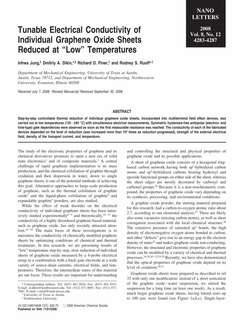
The differential 4-probe technique and three differentlayouts of electrodes (separated by 10 to 50 µm), as shownin Figures 1a,b,c, were fabricated by one-step photolithog-raphy with an initial goal of looking for possible anisotropyin individual sheet conductivity. All of the reported electricalmeasurements were taken in a vacuum chamber (∼10-5 Torr)evacuated for at least 1 h prior to the start of the experiment.Eighteen individual graphene oxide devices were measuredin total (details in the Supporting Information). The irregularshape of the graphene oxide sheets and the position of theelectrodes relative to their edges (van der Pauw configuration)called for data analysis that was performed numerically byusing a finite elements method (see Supporting Informationfor details about device preparation, measurements, and dataanalysis). Electrical anisotropy in the conductance of thegraphene oxide sheets was not observed.
Sample electrical resistance was used as a real-timeindicator of graphene oxide chemical/structural modification.By controlling the temperature of the hot plate and the timeof heating, we were able to gradually recover the grapheneoxide sheet conductivity. Figure 1d shows the tempera-ture profile as a function of time and the correspondingresistance change for one of the samples; a heating rate of∼1 °C/min was used. Four interruptions of heating, withsubsequent cool down to room temperature each of the fourtimes, were made at 172 (point 1), 138 (point 2), 152 (point3), and 165 °C (point 4). Data prior to point 1 (Figure 1d)are not shown because no measurable resistance was recorded
until that time. As indicated in Figure 1d, as soon as the“measurable” thermal reduction had begun at about 160 °C,reduction continues (resistance decreases) after each repeatedcooling and heating as the increased temperature reachesabout 125 ( 5 °C. At the fourth heating, the change in thesample resistance exhibited saturation (see red curve ap-proaching minute 800). The sample resistance thus droppedfrom essentially infinity to about 2 MΩ for this heatingprotocol.
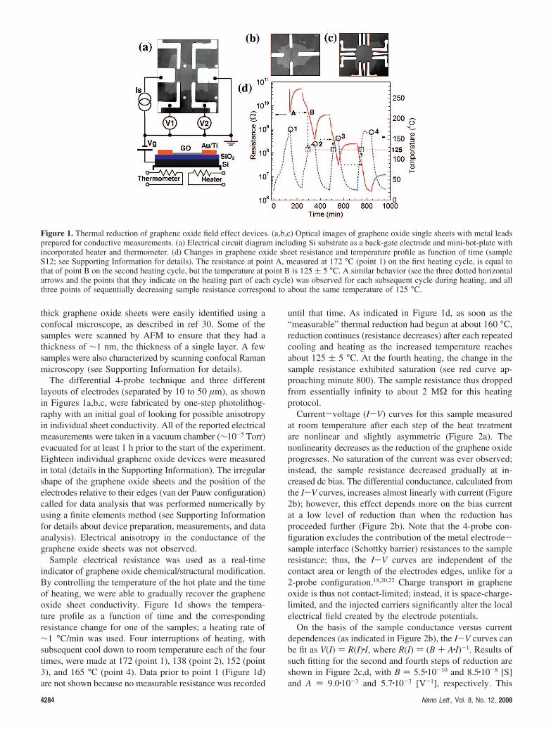
Current-voltage (I-V) curves for this sample measuredat room temperature after each step of the heat treatmentare nonlinear and slightly asymmetric (Figure 2a). Thenonlinearity decreases as the reduction of the graphene oxideprogresses. No saturation of the current was ever observed;instead, the sample resistance decreased gradually at in-creased dc bias. The differential conductance, calculated fromthe I-V curves, increases almost linearly with current (Figure2b); however, this effect depends more on the bias currentat a low level of reduction than when the reduction hasproceeded further (Figure 2b). Note that the 4-probe con-figuration excludes the contribution of the metal electrode-sample interface (Schottky barrier) resistances to the sampleresistance; thus, the I-V curves are independent of thecontact area or length of the electrodes edges, unlike for a2-probe configuration.18,20,22 Charge transport in grapheneoxide is thus not contact-limited; instead, it is space-charge-limited, and the injected carriers significantly alter the localelectrical field created by the electrode potentials.
On the basis of the sample conductance versus currentdependences (as indicated in Figure 2b), the I-V curves canbe fit as V(I) ) R(I)·I, where R(I) ) (B + A·I)-1. Results ofsuch fitting for the second and fourth steps of reduction areshown in Figure 2c,d, with B ) 5.5·10-10 and 8.5·10-8 [S]and A ) 9.0·10-3 and 5.7·10-3 [V-1], respectively. This
Figure 1. Thermal reduction of graphene oxide field effect devices. (a,b,c) Optical images of graphene oxide single sheets with metal leadsprepared for conductive measurements. (a) Electrical circuit diagram including Si substrate as a back-gate electrode and mini-hot-plate withincorporated heater and thermometer. (d) Changes in graphene oxide sheet resistance and temperature profile as function of time (sampleS12; see Supporting Information for details). The resistance at point A, measured at 172 °C (point 1) on the first heating cycle, is equal tothat of point B on the second heating cycle, but the temperature at point B is 125 ( 5 °C. A similar behavior (see the three dotted horizontalarrows and the points that they indicate on the heating part of each cycle) was observed for each subsequent cycle during heating, and allthree points of sequentially decreasing sample resistance correspond to about the same temperature of 125 °C.
4284 Nano Lett., Vol. 8, No. 12, 2008
approach describes the I-V data perfectly at the highest levelof reduction (Figure 2d), whereas at the early reduction level,some deviation is observed (Figure 2c). Thus, our assumptionthat graphene oxide conductivity is linearly dependent onthe amount of injected charges, σ ∼ I ∼ n, is correct for thehigh reduction level.
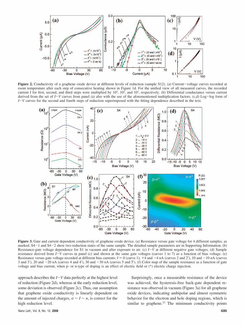
Surprisingly, once a measurable resistance of the devicewas achieved, the hysteresis-free back-gate dependent re-sistance was observed in vacuum (Figure 3a) for all grapheneoxide devices, indicating ambipolar and almost symmetricbehavior for the electron and hole doping regions, which issimilar to graphene.33 The minimum conductivity points
Figure 2. Conductivity of a graphene oxide device at different levels of reduction (sample S12). (a) Current-voltage curves recorded atroom temperature after each step of consecutive heating shown in Figure 1d. For the unified view of all measured curves, the recordedcurrent I for first, second, and third steps were multiplied by 103, 102, and 101, respectively. (b) Differential conductance versus currentderived from the set of I-V curves from panel (a) also with the use of the aforementioned multiplication factors. (c,d) Log-log form ofI-V curves for the second and fourth steps of reduction superimposed with the fitting dependence described in the text.
Figure 3. Gate and current dependent conductivity of graphene oxide device. (a) Resistance versus gate voltage for 4 different samples, asmarked. S4-1 and S4-2 show two reduction states of the same sample. The detailed sample parameters are in Supporting Information. (b)Resistance-gate voltage dependence for S1 in vacuum and after exposure to air. (c) I-V at different negative gate voltages. (d) Sampleresistance derived from I-V curves in panel (c) and shown at the same gate voltages (curves 1 to 7) as a function of bias voltage. (e)Resistance versus gate voltage recorded at different bias currents: I ) 0 (curve 1), +4 and -4 nA (curves 2 and 2′), 10 and -10 nA (curves3 and 3′), 20 and -20 nA (curves 4 and 4′), 30 and -30 nA (curves 5 and 5′). (f) Color map of the sample resistance as a function of gatevoltage and bias current, when p- or n-type of doping is an effect of electric field or (*) electric charge injection.
Nano Lett., Vol. 8, No. 12, 2008 4285

(MCP, or the Dirac point) usually had small gate voltageoffset (both polarities were observed), despite the fact thatthe resistivity decays slowly for the entire range of appliedfields. This is unlike the behavior of weakly disorderedgraphene.6 Any short exposure of graphene oxide devicesto the room environment or water vapor led to a rise ofhysteretic response to a back-gate potential, since adsorbedmolecules, e.g., water, become polarized inthe applied electric field (Figure 3b). If the graphene oxidedevice was placed back in the vacuum chamber (10-5 Torr),the measured hysteresis slowly decreased, but it did notcompletely vanish until the device was heated to a temper-ature slightly above 100 °C for approximately 20 min. Theremaining chemical groups covalently bound to the carbonskeleton did not reveal any obvious polarization or chargingbehavior at a relatively slow sweep rate (0.1 V/s).
Figure 3c,d shows an example of how, initially, almostsymmetric n- and p-type conductance was transformed to,e.g., a p-dominated conductance due to a negative gatepotential. The same type of transformation was observed viainjecting positive or negative charges into a graphene oxidesheet. Subject to these conditions, in both the hole- andelectron-accumulation regimes, the I-V curves become lessnonlinear but more asymmetric, as can be seen in Figure3c. As a result, the MCP moves toward the positive ornegative gate potential (see Figure 3e). On the basis of thesedata, an equivalent change in the carrier charge density perunit-surface due to the “injection doping” of graphene oxidecan be estimated. The gate potential, applied across the 300-nm-thick SiO2 layer, induces changes in the surface chargedensity n ) ε0εVg/(te) ≈ 7.2·1010 cm-2 per 1 V, where ε0
and ε are the permittivity of free space and of the silicondioxide having thickness t, and e is the electron charge. Asseen in Figure 3e, 4 nA of injected current leads to a shiftof the MCP to +20 or -20 V of the gate voltage, dependingon the dc current polarity. Thus, the shift of the MCP canbe recalculated as an equivalent change of the charge densityin the following way: 20 V × 7.2·1010 ·cm-2 V-1 ) 1.44·1012
cm-2, when a (40 nA bias current corresponds to an MCP
shift of (47 V of the gate voltage and is equivalent to a∼3.38·1012 cm-2 change in the carrier density. Followingthe conventional MOSFET model, when a negative gatepotential is applied, a positive dc bias will recover electronloss and restore the n-channel transistor, and a negative dcbias will enhance the p-channel-dominated behavior. Thetwo-dimensional resistance plot (Figure 3f) summarizes thecombined effect of n- or p-doping via electrical field and dcbias charge (n* or p*) injection. Away from the MCP centralarea, cooperative p-p* or n-n* conductivity enhancement(lower left and upper right corners in Figure 3f) is seen asnegative (positive) gate potential and negative (positive) bias,respectively, or as a noncooperative competing contributionof these two factors (upper left and lower right corners in Figure3f). This behavior looks similar to graphene conductivitycontrolled by a combination of top and back gates.34 Thus,both p- and n-carriers are seen in the percolating conductivityof the graphene oxide sheets and their value can be tunedby the gate potential or by charge-injection doping.
The reduced graphene oxide sheet shows a significant increasein resistance upon cooling after each reduction step (Figures 1dand 4a). The likely continued reduction during slow samplecooldown and the narrow temperature interval prohibits moredetailed analysis, although one can see that the temperaturecoefficient of resistance (TCR) is going down as the reductionprogresses (see Figure 4a), indicating a decrease in thesemiconducting energy gap. The gate-dependent resistance(measured at 1 nA) also exhibits a significant change vstemperature (Figure 4b). Small n-type dominated conductiv-ity at room temperature is transformed upon heating to amuch larger electron-doped conductivity with significantlyreduced gate dependence. A close similarity with Figure 3dis seen, but in this case, the overall charge transport iscontrolled by thermal activation instead of carrier injection.
By analogy with a cluster model of amorphous andhydrogenated amorphous carbon,35 graphene oxide containsboth sp2 and, predominantly, amorphous sp3 sites, and canbe described as a quasi two-dimensional amorphous carbon(a-C). A complex set of hydroxyl-hydroxyl and hydroxyl-
Figure 4. Temperature dependences of graphene oxide device. (a) The normalized-to-room temperature sample resistance versus temperaturerecorded at cooldown as shown in Figure 1d (sample S12). Temperature coefficients of resistance after the second, third, and fourth reductionsaccording to linear fits are -11.0·10-3, -8.9·10-3, and -7.4·10-3 K-1, respectively. (b) Resistance as a function of gate voltage measuredat 4 different temperatures (sample S12).
4286 Nano Lett., Vol. 8, No. 12, 2008
epoxide hydrogen-bonding interactions takes place betweenthe functional groups of graphene oxide. The moleculardynamics simulations36 reveal reactions in which hydrogenatoms are transferred and epoxide groups migrate on the basalplane stabilizing by hydrogen bonding or catalyzing byhydrogen transfer reactions between the mobile epoxideoxygen and neighboring functional groups. Thus, initiallythe sp2 clusters in graphene oxide are small and separatedby an amorphous and highly disordered sp3 bonded matrix,which forms a high tunnel barrier between the clusters.During heat treatment, the thermal energy favors the furtherclustering of the sp2 phase stimulating connection betweenordered rings and moving from amorphous to the two-dimensional nanocrystaline graphene, as was outlined in ref37. This transformation results in the increase of I(D)/I(G)ratio and a shift in the position of the G peak (see Figure 4in ref 37). The equation for nanocrystalline sizes,38,39 La, isinvalid in this stage of chemically modified graphene (seedetails in the Supporting Information). However, much moreresearch is required to understand all details of this newmaterial’s behavior.
A possible simplified model for the graphene oxideconductance is that of percolation in random continua:40 thetwo-dimensional Swiss-cheese model. As reduction progresses,a sample-spanning cluster of touching conductive regions isformed, and the sample resistance exhibits a power lawdecay. That is, the localized states are randomly dispersedthroughout the graphene oxide. The model is complicatedby the fact that the occupation of the localized states iscontrolled by the superposition of gate voltage and localelectric field created by the amount of injected carriers, andhopping between localized states is thermally assisted.Adequate modeling of such a system will require a host ofadditional experiments.
Graphene oxide is unique compared to graphene in thatits electrical conductivity and optical transparency dramati-cally depends on the level of oxidation. Such chemicallytuned graphene sheets already suggest new vistas2,18,20,21,41
and hold significant promise for novel sensors, membrane-based NEMS devices, transparent conductors for optoelec-tronic applications, smart composite materials, and others.
Acknowledgment. The authors thank S. Stankovich formaking graphite oxide. I.J., D.A.D., and R.S.R. acknowledgefunding from the DARPA N/MEMS S&T FundamentalsProgram.
Supporting Information Available: Fabrication proce-dure, detailed description of the devices, analysis of theirconductivity, and Raman spectroscopy results. This materialis available free of charge via the Internet at http://pubs.acs.org.
References(1) Geim, A. K.; Novoselov, K. S. Nat. Mater. 2007, 6, 183.(2) Stankovich, S.; Dikin, D. A.; Dommett, G. H. B.; Kohlhaas, K. M.;
Zimney, E. J.; Stach, E. A.; Piner, R. D.; Nguyen, S. T.; Ruoff, R. S.Nature 2006, 442, 282.
(3) Schniepp, H. C.; Li, J. L.; McAllister, M. J.; Sai, H.; Herrera-Alonso,M.; Adamson, D. H.; Prud’homme, R. K.; Car, R.; Saville, D. A.;Aksay, I. A. J. Phys. Chem. B 2006, 110, 8535.
(4) Hernandez, Y.; Nicolosi, V.; Lotya, M.; Blighe, F. M.; Sun, Z.; De,S.; T., M.; Holland, B.; Byrne, M.; Gun’Ko, Y. K.; Boland, J. J.; Niraj,
P.; Duesberg, G.; Krishnamurthy, S.; Goodhue, R.; Hutchison, J.;Scardaci, V.; Ferrari, A. C.; Coleman, J. N. Nat. Nanotechnol. 2008,3, 563.
(5) Li, X.; Zhang, G.; Bai, X.; Sun, X.; Wang, X.; Wang, E.; Dai, H.Nat. Nanotechnol. 2008, 3, 538.
(6) Tan, Y. W.; Zhang, Y.; Bolotin, K.; Zhao, Y.; Adam, S.; Hwang,E. H.; Das Sarma, S.; Stormer, H. L.; Kim, P. Phys. ReV. Lett. 2007,99, 246803.
(7) Cho, S.; Fuhrer, M. S. Phys. ReV. B 2008, 77, 081402.(8) Martin, J.; Akerman, N.; Ulbricht, G.; Lohmann, T.; Smet, J. H.; Von
Klitzing, K.; Yacoby, A. Nat. Phys. 2008, 4, 144.(9) Wehling, T. O.; Novoselov, K. S.; Morozov, S. V.; Vdovin, E. E.;
Katsnelson, M. I.; Geim, A. K.; Lichtenstein, A. I. Nano Lett. 2008,8, 173.
(10) Pereira, V. M.; Guinea, F.; dos Santos, J.; Peres, N. M. R.; Neto,A. H. C. Phys. ReV. Lett. 2006, 96, 036801.
(11) Cheianov, V. V.; Fal’ko, V. I.; Altshuler, B. L.; Aleiner, I. L. Phys.ReV. Lett. 2007, 99, 176801.
(12) Fogler, M. M.; Novikov, D. S.; Shklovskii, B. I. Phys. ReV. B 2007,76, 233402.
(13) de Juan, F.; Cortijo, A.; Vozmediano, M. A. H. Phys. ReV. B 2007,76, 165409.
(14) Guinea, F.; Katsnelson, M. I.; Vozmediano, M. A. H. Phys. ReV. B2008, 77, 075422.
(15) Dora, B.; Ziegler, K.; Thalmeier, P. Phys. ReV. B 2008, 77, 115422.(16) Gomez-Navarro, C.; Weitz, R. T.; Bittner, A. M.; Scolari, M.; Mews,
A.; Burghard, M.; Kern, K. Nano Lett. 2007, 7, 3499.(17) Wu, X. S.; Li, X. B.; Song, Z. M.; Berger, C.; de Heer, W. A. Phys.
ReV. Lett. 2007, 98, 136801.(18) Gilje, S.; Han, S.; Wang, M.; Wang, K. L.; Kaner, R. B. Nano Lett.
2007, 7, 3394.(19) McAllister, M. J.; LiO, J. L.; Adamson, D. H.; Schniepp, H. C.; Abdala,
A. A.; Liu, J.; Herrera-Alonso, M.; Milius, D. L.; CarO, R.;Prud’homme, R. K.; Aksay, I. A. Chem. Mater. 2007, 19, 4396.
(20) Eda, G.; Fanchini, G.; Chhowalla, M. Nat. Nanotechnol. 2008, 3, 270.(21) Becerril, H. A.; Mao, J.; Liu, Z.; Stoltenberg, R. M.; Bao, Z.; Chen,
Y. ACS Nano 2008, 2, 463.(22) Wu, X. S.; Sprinkle, M.; Li, X. B.; Ming, F.; Berger, C.; de Heer,
W. A. Phys. ReV. Lett. 2008, 101, 026801.(23) Li, D.; Muller, M. B.; Gilje, S.; Kaner, R. B.; Wallace, G. G. Nat.
Nanotechnol. 2008, 3, 101.(24) Wang, X.; Zhi, L. J.; Mullen, K. Nano Lett. 2008, 8, 323.(25) Boukhvalov, D. W.; Katsnelson, M. I. J. Am. Chem. Soc. 2008, 130,
10697.(26) Szabo, T.; Berkesi, O.; Forgo, P.; Josepovits, K.; Sanakis, Y.; Petridis,
D.; Dekany, I. Chem. Mater. 2006, 18, 2740.(27) Stankovich, S.; Piner, R. D.; Chen, X. Q.; Wu, N. Q.; Nguyen, S. T.;
Ruoff, R. S. J. Mater. Chem. 2006, 16, 155.(28) Cortijo, A.; Vomediano, M. A. H. Nucl. Phys. B 2007, 763, 293.(29) Stankovich, S.; Dikin, D. A.; Piner, R. D.; Kohlhaas, K. A.;
Kleinhammes, A.; Jia, Y.; Wu, Y.; Nguyen, S. T.; Ruoff, R. S. Carbon2007, 45, 1558.
(30) Jung, I.; Pelton, M.; Piner, R.; Dikin, D. A.; Stankovich, S.;Watcharotone, S.; Hausner, M.; Ruoff, R. S. Nano Lett. 2007, 7, 3569.
(31) Jung, I.; Vaupel, M.; Pelton, M.; Piner, R.; Dikin, D. A.; Stankovich,S.; An, J.; Ruoff, R. S. J. Phys. Chem. C 2008, 112, 8499.
(32) Dikin, D. A.; Stankovich, S.; Zimney, E. J.; Piner, R. D.; Dommett,G. H. B.; Evmenenko, G.; Nguyen, S. T.; Ruoff, R. S. Nature 2007,448, 457.
(33) Novoselov, K. S.; Geim, A. K.; Morozov, S. V.; Jiang, D.; Zhang,Y.; Dubonos, S. V.; Grigorieva, I. V.; Firsov, A. A. Science 2004,306, 666.
(34) Williams, J. R.; DiCarlo, L.; Marcus, C. M. Science 2007, 317, 638.(35) Robertson, J.; Oreilly, E. P. Phys. ReV. B 1987, 35, 2946.(36) Paci, J. T.; Belytschko, T.; Schatz, G. C. J Phys. Chem. C 2007, 111,
18099.(37) Ferrari, A. C.; Robertson, J. Philos. Trans. R. Soc. Lond., Ser. A: Math.
Phys. Eng. Sci. 2004, 362, 2477.(38) Tuinstra, F.; Koenig, J. L. J. Chem. Phys. 1970, 53, 1126.(39) Pimenta, M. A.; Dresselhaus, G.; Dresselhaus, M. S.; Cancado, L. G.;
Jorio, A.; Saito, R. Phys. Chem. Chem. Phys. 2007, 9, 1276.(40) Balberg, I. Phil. Mag. B 1987, 56, 991.(41) Watcharotone, S.; Dikin, D. A.; Stankovich, S.; Piner, R.; Jung, I.;
Dommett, G. H. B.; Evmenenko, G.; Wu, S. E.; Chen, S. F.; Liu,C. P.; Nguyen, S. T.; Ruoff, R. S. Nano Lett. 2007, 7, 1888.
NL8019938
Nano Lett., Vol. 8, No. 12, 2008 4287