Embed Size (px)
DESCRIPTION
GM By ID design thesis
Citation preview

Automatic Reusable Design for AnalogMicropower Integrated Circuits
Por
Pablo Aguirre
Tesis Presentada Ante elInstituto de Ingenierıa Electrica
Para Cumplir con Parte delos Requisitos del Grado de
MAGISTER EN INGENIERıA ELECTRICA
En el Area de MICROELECTRONICA
Tutor:
Prof. Fernando Silveira
Tribunal:
Prof. Jose Silva-Martinez, Texas A&M, USA.
Prof. Carlos Galup-Montoro, UFSC, Brasil.
Prof. Gregory Randall, UDELAR, Uruguay.
Instituto de Ingenierıa ElectricaFacultad de Ingenierıa
Universidad de la RepublicaMontevideo, Uruguay
Abril 2004

ISSN: 1510-7264
Typesetted in LATEX2ε
Contents
List of Figures . . . . . . . . . . . . . . . . . . . . . . . . . . . . . . . . . . . vi
List of Tables . . . . . . . . . . . . . . . . . . . . . . . . . . . . . . . . . . . . ix
List of Algorithms . . . . . . . . . . . . . . . . . . . . . . . . . . . . . . . . . x
Agradecimientos . . . . . . . . . . . . . . . . . . . . . . . . . . . . . . . . . . xi
Resumen . . . . . . . . . . . . . . . . . . . . . . . . . . . . . . . . . . . . . . xiii
Abstract . . . . . . . . . . . . . . . . . . . . . . . . . . . . . . . . . . . . . . . xv
1. Introduction . . . . . . . . . . . . . . . . . . . . . . . . . . . . . . . . . . . 1
2. Design Methodologies . . . . . . . . . . . . . . . . . . . . . . . . . . . . . . 5
2.1 Introduction . . . . . . . . . . . . . . . . . . . . . . . . . . . . . . . . 5
2.2 A Current-Based MOSFET Model for IC Design . . . . . . . . . . . . 5
2.2.1 Current - Voltage Relationships . . . . . . . . . . . . . . . . . 6
2.2.2 The (gm/ID) Ratio . . . . . . . . . . . . . . . . . . . . . . . . 7
2.2.3 Intrinsic Capacitances . . . . . . . . . . . . . . . . . . . . . . 7
2.2.4 Noise Model . . . . . . . . . . . . . . . . . . . . . . . . . . . . 8
2.2.5 Output Conductance . . . . . . . . . . . . . . . . . . . . . . . 10
2.2.6 Non-quasi-static Model and Second Order Effects . . . . . . . 10
2.2.7 Why ACM? . . . . . . . . . . . . . . . . . . . . . . . . . . . . 10
2.3 The (gm/ID) Based Methodology for Analog Design . . . . . . . . . . 10
2.4 Automatic Synthesis for Miller Amplifiers . . . . . . . . . . . . . . . 12
2.4.1 The Miller Amplifier . . . . . . . . . . . . . . . . . . . . . . . 12
2.4.2 Gain-Bandwidth Driven Synthesis Algorithm . . . . . . . . . . 17
2.4.3 Design Optimization Through Design Space Exploration . . . 17
2.4.4 Synthesis Example: Micropower 100kHz Miller Amplifier . . . 19
2.4.5 Synthesis Example: 50MHz Miller Amplifier . . . . . . . . . . 25
2.5 Conclusions . . . . . . . . . . . . . . . . . . . . . . . . . . . . . . . . 29
3. Low-Power OpAmp Cells: Reuse, Architecture and Synthesis . . . . . . . . 31
3.1 Introduction . . . . . . . . . . . . . . . . . . . . . . . . . . . . . . . . 31
3.2 Analog Design Reuse . . . . . . . . . . . . . . . . . . . . . . . . . . . 31
iii

3.2.1 Circuit Performance Tuning Through Bias Current . . . . . . 32
3.2.2 Reusable Circuit Architectures . . . . . . . . . . . . . . . . . . 36
3.2.3 Technology Migration . . . . . . . . . . . . . . . . . . . . . . . 39
3.3 Opamp Architecture . . . . . . . . . . . . . . . . . . . . . . . . . . . 40
3.3.1 Constant gm Rail-to-Rail Input Stages . . . . . . . . . . . . . 40
3.3.2 Low-Power Class AB Output Stage . . . . . . . . . . . . . . . 45
3.3.3 Opamp Complete Architecture . . . . . . . . . . . . . . . . . 48
3.4 Advanced Design Methodologies . . . . . . . . . . . . . . . . . . . . . 48
3.4.1 Power Optimization for a Given Total Settling Time . . . . . 49
3.4.2 Settling Behavior Model . . . . . . . . . . . . . . . . . . . . . 50
3.4.3 Power Optimization of a Miller OTA . . . . . . . . . . . . . . 51
3.5 Conclusions . . . . . . . . . . . . . . . . . . . . . . . . . . . . . . . . 53
4. Hierarchical Automated Synthesis . . . . . . . . . . . . . . . . . . . . . . . 55
4.1 Introduction . . . . . . . . . . . . . . . . . . . . . . . . . . . . . . . . 55
4.2 Miller Compensation Capacitance for Minimum Power Consumption . 55
4.3 Synthesis Algorithm . . . . . . . . . . . . . . . . . . . . . . . . . . . 56
4.3.1 High Level Synthesis . . . . . . . . . . . . . . . . . . . . . . . 58
4.3.2 Input Stage Synthesis . . . . . . . . . . . . . . . . . . . . . . . 61
4.3.3 Output Stage Synthesis . . . . . . . . . . . . . . . . . . . . . . 65
4.4 Synthesis Results . . . . . . . . . . . . . . . . . . . . . . . . . . . . . 69
4.4.1 1µs Settling Time Design . . . . . . . . . . . . . . . . . . . . 70
4.4.2 Opamp Performance Tuning . . . . . . . . . . . . . . . . . . . 75
4.4.3 Synthesized vs. Tuned . . . . . . . . . . . . . . . . . . . . . . 78
4.4.4 Performance Evaluation Against a Simpler Architecture . . . . 78
4.5 Analysis of the Constant-gm Circuit . . . . . . . . . . . . . . . . . . . 79
4.5.1 Open Loop Transfer . . . . . . . . . . . . . . . . . . . . . . . 80
4.5.2 Bias Current Monitor . . . . . . . . . . . . . . . . . . . . . . . 82
4.5.3 Redesign of the Constant-gm Circuit . . . . . . . . . . . . . . 83
4.6 Conclusions . . . . . . . . . . . . . . . . . . . . . . . . . . . . . . . . 84
5. Experimental Results . . . . . . . . . . . . . . . . . . . . . . . . . . . . . . 85
5.1 Rail-to-rail Operational Amplifier in 0.8µm CMOS Technology . . . . 85
5.2 Comparison with other published results . . . . . . . . . . . . . . . . 90
5.3 Conclusions . . . . . . . . . . . . . . . . . . . . . . . . . . . . . . . . 92
iv

6. Conclusions . . . . . . . . . . . . . . . . . . . . . . . . . . . . . . . . . . . 93
A. Low-Voltage Cascode Bias Transistor Design . . . . . . . . . . . . . . . . . 97
B. Size of Transistors in the Experimental Prototype . . . . . . . . . . . . . . 99
Bibliography . . . . . . . . . . . . . . . . . . . . . . . . . . . . . . . . . . . . 101
v

List of Figures
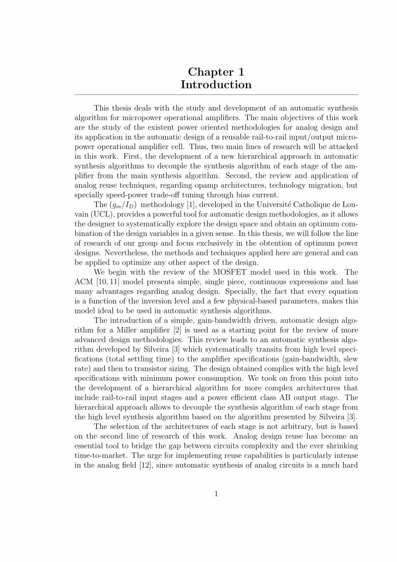
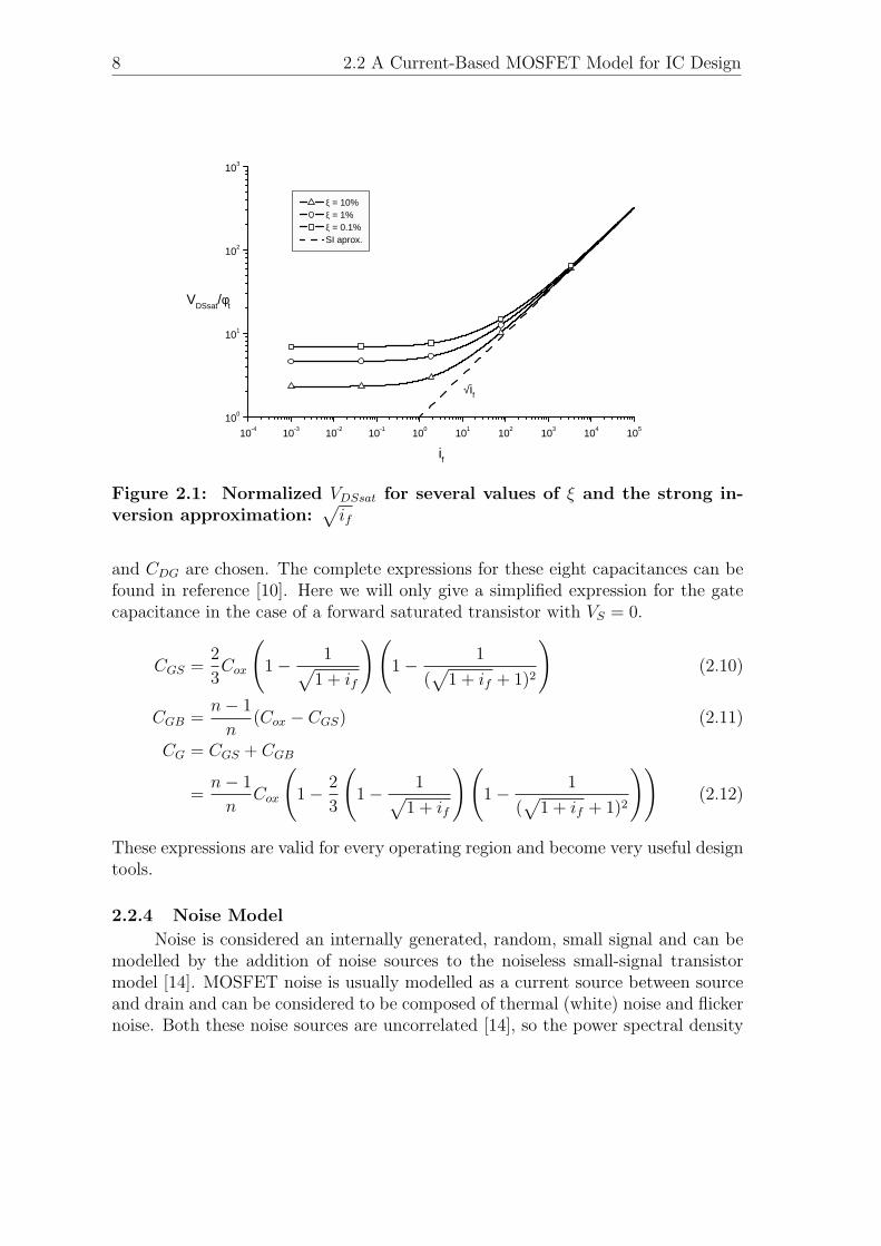
2.1 Normalized VDSsat for several values of ξ and the SI approximation . . . 8
2.2 (gm/ID) ratio as a function of the inversion factor if . . . . . . . . . . . 11
2.3 Miller Amplifier, including parasitics capacitances. . . . . . . . . . . . . 13
2.4 Offset voltage as a function of (gm/ID) . . . . . . . . . . . . . . . . . . 16
2.5 Design space exploration: Total consumption (in µA) of the 100kHzMiller Amplifier. . . . . . . . . . . . . . . . . . . . . . . . . . . . . . . . 20
2.6 Design space exploration: Die area estimation (in µm2) of the 100kHzMiller Amplifier.. . . . . . . . . . . . . . . . . . . . . . . . . . . . . . . 21
2.7 Design space exploration: DC Gain (in dB) of the 100kHz Miller Am-plifier.. . . . . . . . . . . . . . . . . . . . . . . . . . . . . . . . . . . . . 21
2.8 Gain and doublet frequency dependence on the length of M3. . . . . . . 23
2.9 Output swing and total area dependence on (gm/ID)4 ratio. . . . . . . 23
2.10 Gain and total area dependence on the length of M4. . . . . . . . . . . 24
2.11 Frequency response of the 100kHz Miller Amplifier. . . . . . . . . . . . 26
2.12 Design space exploration: Total consumption (in mA) of the 50MHzMiller Amplifier. . . . . . . . . . . . . . . . . . . . . . . . . . . . . . . . 27
2.13 Design space exploration: Die area estimation (in µm2) of the 50MHzMiller Amplifier. . . . . . . . . . . . . . . . . . . . . . . . . . . . . . . . 27
2.14 Design space exploration: Total gain (in dB) of the 50MHz Miller Am-plifier. . . . . . . . . . . . . . . . . . . . . . . . . . . . . . . . . . . . . 28
2.15 Frequency response of the 50MHz Miller Amplifier. . . . . . . . . . . . . 29
3.1 Gain-Bandwidth product tuning of the Miller amplifier from section 2.4.4 33
3.2 General characteristic of the class AB stage. . . . . . . . . . . . . . . . 38
3.3 Open loop frequency response comparison in technology migration . . . 40
3.4 Basic rail-to-rail differential pair architecture. . . . . . . . . . . . . . . . 41
3.5 Transconductance as a function of the input common mode voltage,using architecture from Figure 3.4. . . . . . . . . . . . . . . . . . . . . . 42
vi

3.6 Schematic view of the constant gm operation principle. . . . . . . . . . 43
3.7 Implementation of the constant gm technique . . . . . . . . . . . . . . . 44
3.8 Transconductance as a function of the input common mode voltageusing constant gm technique. . . . . . . . . . . . . . . . . . . . . . . . . 45
3.9 Class AB output stage . . . . . . . . . . . . . . . . . . . . . . . . . . . 46
3.10 Amplifier circuit implementation, omitting constant-gm circuit. . . . . . 48
3.11 Settling time model and step response plot. . . . . . . . . . . . . . . . . 50
4.1 High Level Schematic of the Amplifier . . . . . . . . . . . . . . . . . . . 57
4.2 Complete Amplifier Synthesis Algorithm Scheme. tsett is total settlingtime and IDD is total current consumption. . . . . . . . . . . . . . . . 58
4.3 Folded Cascode Circuit . . . . . . . . . . . . . . . . . . . . . . . . . . . 63
4.4 Class AB output stage. . . . . . . . . . . . . . . . . . . . . . . . . . . . 65
4.5 Opamp cell, omitting constant-gm circuitry . . . . . . . . . . . . . . . . 69
4.6 Total Consumption (in µA) for a 1µsec total settling time rail-to-railOTA . . . . . . . . . . . . . . . . . . . . . . . . . . . . . . . . . . . . . 70
4.7 Transition frequency and Phase Margin along the input common moderange. . . . . . . . . . . . . . . . . . . . . . . . . . . . . . . . . . . . . . 73
4.8 Total Settling Time for different input common mode range . . . . . . . 74
4.9 Transition frequency (fT ) and Phase Margin tuning over more than 3decades . . . . . . . . . . . . . . . . . . . . . . . . . . . . . . . . . . . . 75
4.10 Transition frequency and phase margin tuning as a function of the inputcommon mode . . . . . . . . . . . . . . . . . . . . . . . . . . . . . . . . 76
4.11 Total Settling Time tuning for three different input common modes . . 77
4.12 Total Settling Time tuning as a function of the input common moderange . . . . . . . . . . . . . . . . . . . . . . . . . . . . . . . . . . . . . 78
4.13 Total Settling Time comparison between the 10µs design and the tuned1µs design. . . . . . . . . . . . . . . . . . . . . . . . . . . . . . . . . . . 79
4.14 Constant-gm circuit loop. . . . . . . . . . . . . . . . . . . . . . . . . . . 81
4.15 Settling time as a function of the input common mode with the redesignof the constant-gm circuit . . . . . . . . . . . . . . . . . . . . . . . . . . 83
vii

5.1 Opamp Cell Microphotograph . . . . . . . . . . . . . . . . . . . . . . . 85
5.2 Settling time automatic measurement system . . . . . . . . . . . . . . . 86
5.3 Total settling time tuning as a function of the input common mode range 87
5.4 Comparison between the simulated and experimental total settling timetuning for three different input common modes . . . . . . . . . . . . . . 87
5.5 Settling time as a function of the total quiescent current consumption. . 88
5.6 Offset voltage as a function of the input common mode. . . . . . . . . . 90
A.1 Cascode transistor bias. . . . . . . . . . . . . . . . . . . . . . . . . . . . 97
viii

List of Tables
2.1 Specifications for a Micropower 100kHz Miller Amplifier . . . . . . . . . 20
2.2 Final design for a 100kHz Miller amplifier. . . . . . . . . . . . . . . . . 25
2.3 Specifications for a 50MHz Miller Amplifier . . . . . . . . . . . . . . . . 25
2.4 Final design for a 50MHz Miller amplifier. . . . . . . . . . . . . . . . . 28
3.1 Tuning of the Miller amplifier introduced on section 2.4.4 . . . . . . . . 36
4.1 Automatic Synthesis Result with Algorithm 4.1 . . . . . . . . . . . . . 71
4.2 Transistors Sizes Obtained Using Algorithm 4.1 . . . . . . . . . . . . . 72
4.3 Calculated and simulated characteristics of the OTA with 1µsec totalsettling time . . . . . . . . . . . . . . . . . . . . . . . . . . . . . . . . . 73
4.4 Comparison between the 10µs design and the tuned 1µs design. . . . . 80
4.5 Comparison between our amplifier and a simple Miller amplifier desig-ned using Algorithm 3.1 . . . . . . . . . . . . . . . . . . . . . . . . . . . 80
5.1 Opamp Cell characteristics. . . . . . . . . . . . . . . . . . . . . . . . . . 89
5.2 Comparison of the performance of the Opamp Cell. . . . . . . . . . . . 91
B.1 Transistors sizes in the experimental prototype. . . . . . . . . . . . . . . 99
ix
List of Algorithms
2.1 Gain-Bandwidth Driven Automatic Synthesis. . . . . . . . . . . . . . 18
2.2 Power Optimization Automatic Synthesis . . . . . . . . . . . . . . . . 19
3.1 Power Optimization for a Given Total Settling Time . . . . . . . . . . 54
4.1 High Level Synthesis . . . . . . . . . . . . . . . . . . . . . . . . . . . 62
4.2 Input Stage Synthesis . . . . . . . . . . . . . . . . . . . . . . . . . . . 65
4.3 Output Stage Synthesis . . . . . . . . . . . . . . . . . . . . . . . . . . 69
x
Agradecimientos
Si bien esta tesis fue realizada en su totalidad en Uruguay, donde el espanol esla unica lengua oficial, decidimos escribirla en ingles para darle a la misma mayorposibilidad de difusion, ya que como dijo el Prof. Gabor Temes en una conferenciaen la que tuve el gusto de escucharlo “The language of scientific research is accentedenglish”. Podra sorprender, entonces, que estas lıneas esten escritas en espanol, perolo cierto es que todas las personas a las que quiero agradecer tienen la suerte de teneral idioma espanol por lengua madre, por lo que no veo la razon para agradecerlesen otro idioma.
Esta tesis es el resultado del apoyo y el esfuerzo de diversas personas a las queestoy profundamente agradecido.
Mi tutor, Fernando Silveira, ha sido una solida y fundamental guıa en estetrabajo. Fernando ha sido quien, a lo largo de estos anos, me ha brindado desdesu ya amplia experiencia en la investigacion cientıfica lo mejor de sı para formarmecomo investigador en el area de la microelectronica. De hecho, tambien fue el quienme formo en los principios basicos de la electronica en los cursos de grado haceya 4 anos y en los cuales ahora tengo el gusto de desempenarme como uno de susayudantes. A lo largo de estos anos y hasta el dıa de hoy, Fernando siempre estadispuesto a discutir y solucionar mis mas variadas inquietudes, con su habitualoptimismo y a pesar de sus innumerables tareas y obligaciones dentro y fuera de lafacultad. Por todo esto y mucho mas, que probablemente no queda reflejado en estecorto parrafo, estoy sumamente agradecido.
Tambien estoy sumamente agradecido con Alfredo Arnaud, quien por un for-malismo administrativo no puede figurar como el co-tutor que fue de esta tesis.Alfredo ha sido fundamental para este trabajo y en general en mi formacion en lamicroelectronica. Fue el quien me guio en mi primer trabajo en el area y desdeentonces y a lo largo de esta maestrıa nunca ha dudado en apoyarme y asistirmemientras llevaba a cabo exitosamente su propia tesis de doctorado.
Conrado Rossi, con quien compartimos la oficina, ha sido desde que entre en elIIE mi referencia en todo lo que es el funcionamiento del grupo y del propio instituto.Conrado, si bien no participo directamente de este trabajo, siempre estuvo dispuestoa interesarse en el tema y discutir mis dudas, y en los ultimos meses me libero dediversas responsabilidades en el proyecto que el dirige y en el que me desempenocomo ayudante, para que pudiera terminar esta tesis en tiempo y forma.
En ellos, junto al resto del grupo de Microelectronica: Leonardo Barboni,Rafaella Fiorelli, Pablo Mazzara y Linder Reyes, encontre un excelente grupo detrabajo con el que me siento sumamente a gusto y con cuyos integrantes estoy muyagradecido. Aquı tambien quiero agradecer a Raul Acosta, quien trabajo en el temade migracion de tecnologıa y obtuvo los resultados experimentales que se mues-tran en la seccion 3.2.3. Tambien estoy muy agradecido al Instituto de Ingenierıa
xi

Electrica (IIE), a su director, Gregory Randall, y al jefe de mi departamento, RafaelCanetti.
Debo tambien agradecer a la Comision Academica de Posgrados (CAP) de laFacultad de Ingenierıa por la beca de apoyo que me asignaron durante estos casidos anos de trabajo y que me permitio dedicarme exclusivamente a mi maestrıa y ami trabajo docente en el IIE.
Quiero agradecer tambien a los Profesores Carlos Galup-Montoro y Jose SilvaMartinez que aceptaron participar de mi tribunal de tesis. Es un verdadero honorpara mi contar con la evaluacion de dos reconocidos profesores del mas alto nivelinternacional.
Tambien quiero agradecer a la Dra. Adoracion Rueda y a la gente del CNMde Sevilla, Espana, por recibirme y facilitarme los recursos necesarios para realizaruna estancia de investigacion de tres meses durante el ano 2003. Mis tareas en elCNM, si bien no tienen relacion directa con el trabajo de esta tesis, fueron un aporteimportantısimo a mi formacion en esta maestrıa.
Para terminar quiero agradecer a mi familia y amigos. A mis padres quedesde el principio me formaron para dar lo mejor en lo que me propusiera hacer.A mi madre, que es la principal razon para que esta tesis se haya podido escribiren un nivel aceptable de ingles, y a mi padre, que desde que tengo memoria apoyoe incentivo mi fascinacion por las ciencias. A mis hermanos Diego y Fernando,que junto a mis padres, han soportado mis mal humores y que desaparezca de micasa durante largos perıodos de tiempo, otra vez. A Patricia, Choche, Juan Pabloy Agustın quienes desde hace 5 anos me hacen sentir parte de la familia. A misamigos, Ale, Cris, Javo, Jorge, Juan, Leo, Martın, Nacho y Pucho, que siempre meapoyaron y estuvieron mas que dispuestos a ir a comer unos lehmeyuns y tomaruna(s) cerveza(s) despues de un largo dıa de trabajo.
Por ultimo y muy especialmente, a Virigina, quien desde hace ya mas de 5 anosme apoya incondicionalmente y hace lo imposible por entender que es exactamentea lo que se dedica su novio.
xii

Resumen
Esta tesis trata sobre el estudio y desarrollo de un algoritmo automatico de sıntesispara amplificadores operacionales de microconsumo. Los objetivos principales deeste trabajo son el estudio de las metodologıas existentes de diseno analogico paraconsumo mınimo y su aplicacion en el diseno automatico de un amplificador opera-cional reutilizable de microconsumo con etapas de entrada y salida “rail-to-rail”1.Por lo tanto, se seguiran dos lıneas de investigacion en este trabajo. Primero, eldesarrollo de un nuevo enfoque jerarquico en algoritmos de sıntesis automatica, quepermite desacoplar la sıntesis de cada etapa del amplificador del algoritmo de sıntesisprincipal. Segundo, una revision y la aplicacion de tecnicas de reutilizacion de cir-cuitos analogicos, particularmente en arquitecturas de amplificadores, migracion detecnologıa y especialmente en la tecnica de sintonizacion del compromiso entre ve-locidad y consumo utilizando la corriente de polarizacion.
En esta tesis, utilizando la metodologıa (gm/ID) [1], nos enfocaremos exclusi-vamente en la obtencion de disenos con optimo consumo de corriente, siguiendo asıcon la lınea de investigacion del Grupo de Microelectronica del IIE.
El punto de partida para el repaso de las metodologıas de diseno avanzadas, esun algoritmo simple de diseno automatico para un amplificador Miller [2] basado enel producto ganancia por ancho de banda. Este repaso progresa hasta el algoritmode sıntesis automatica desarrollado por Silveira [3], con el cual a partir de especifi-caciones de alto nivel (tiempo total de establecimiento) se puede sistematicamenteobtener las especificaciones del amplificador (producto ganancia por ancho de banda,slew rate) y el tamano de los transistores. El diseno que se obtiene, cumple con lasespecificaciones con consumo mınimo. Desde este punto, desarrollamos un algoritmojerarquico para arquitecturas mas complejas que incluyen etapas de entrada “rail-to-rail” y una etapa de salida clase AB. Este enfoque jerarquico permite separar elalgoritmo de sıntesis de cada etapa del algoritmo de sıntesis de alto nivel que estabasado en el algoritmo presentado por Silveira [3].
La eleccion de las arquitecturas de cada etapa no es arbitraria y esta sumergidaen el contexto de la segunda lınea de investigacion de este trabajo: la reutilizacionde disenos analogicos. En esta linea se investigan dos enfoques. Primero, se estudianarquitecturas para etapas de entrada y salida que son factibles de ser utilizadas endiferentes condiciones de operacion, lo que nos permite obtener una celda que puedeser utilizada en un amplio espectro de aplicaciones para baja tension de alimentaciony microconsumo. El segundo enfoque que se investiga, se centra en la posibilidad desintonizar la performance del circuito mediante la corriente de polarizacion. La ideaes sintonizar el compromiso entre velocidad y consumo del amplificador mientras semantiene la performance en el resto de los aspectos. Esta no es una idea nueva y yaha sido implementada con exito en una aplicacion comercial [4]. Sin embargo, hasta
1Que permiten senales en cualquier nivel de tension entre las fuentes de alimentacion.
xiii
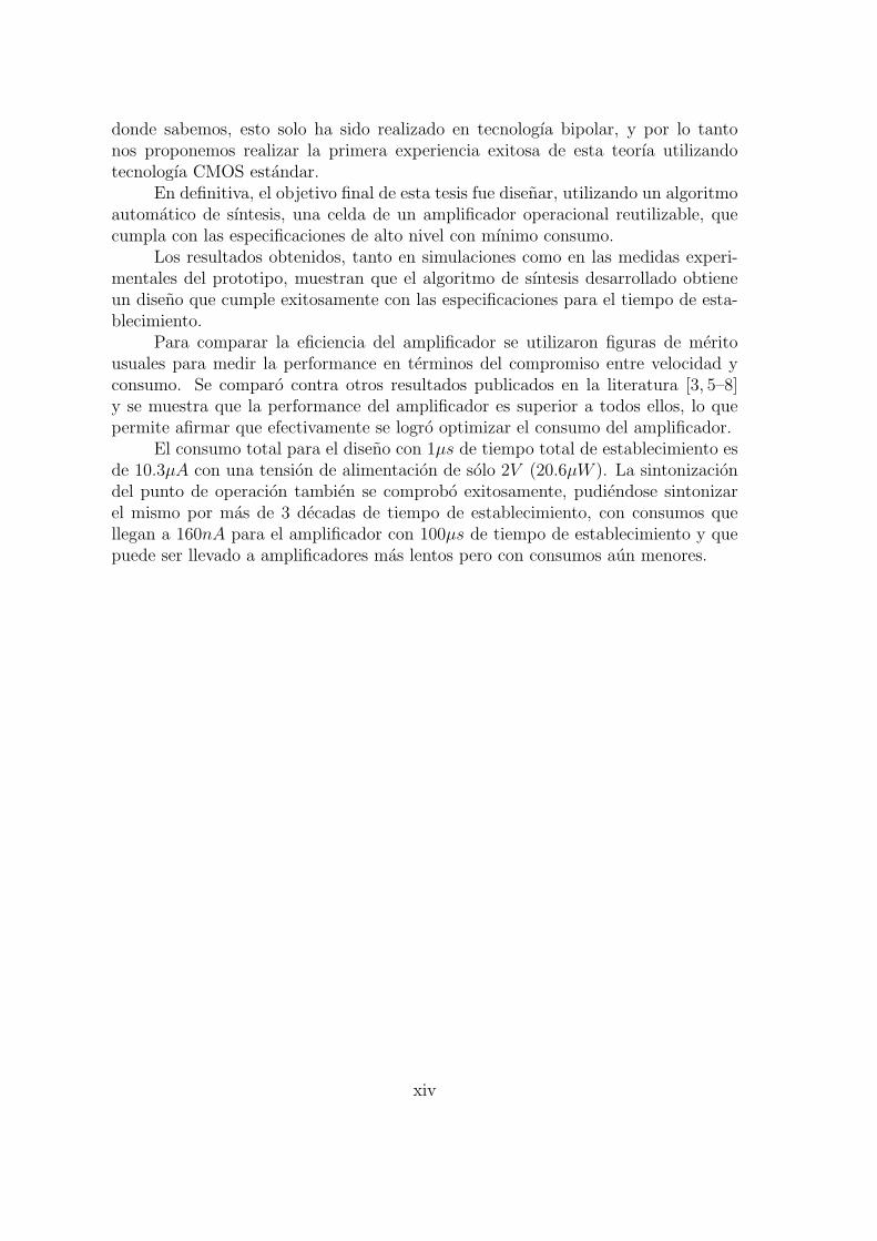
donde sabemos, esto solo ha sido realizado en tecnologıa bipolar, y por lo tantonos proponemos realizar la primera experiencia exitosa de esta teorıa utilizandotecnologıa CMOS estandar.
En definitiva, el objetivo final de esta tesis fue disenar, utilizando un algoritmoautomatico de sıntesis, una celda de un amplificador operacional reutilizable, quecumpla con las especificaciones de alto nivel con mınimo consumo.
Los resultados obtenidos, tanto en simulaciones como en las medidas experi-mentales del prototipo, muestran que el algoritmo de sıntesis desarrollado obtieneun diseno que cumple exitosamente con las especificaciones para el tiempo de esta-blecimiento.
Para comparar la eficiencia del amplificador se utilizaron figuras de meritousuales para medir la performance en terminos del compromiso entre velocidad yconsumo. Se comparo contra otros resultados publicados en la literatura [3, 5–8]y se muestra que la performance del amplificador es superior a todos ellos, lo quepermite afirmar que efectivamente se logro optimizar el consumo del amplificador.
El consumo total para el diseno con 1µs de tiempo total de establecimiento esde 10.3µA con una tension de alimentacion de solo 2V (20.6µW ). La sintonizaciondel punto de operacion tambien se comprobo exitosamente, pudiendose sintonizarel mismo por mas de 3 decadas de tiempo de establecimiento, con consumos quellegan a 160nA para el amplificador con 100µs de tiempo de establecimiento y quepuede ser llevado a amplificadores mas lentos pero con consumos aun menores.
xiv

Abstract
This thesis deals with the study and development of an automatic synthesis algo-rithm for micropower operational amplifiers. The main objectives of this work arethe study of the existent power oriented methodologies for analog design and itsapplication in the automatic design of a reusable rail-to-rail input/output micro-power operational amplifier cell. Thus, two main lines of research will be attackedin this work. First, the development of a new hierarchical approach in automaticsynthesis algorithms to decouple the synthesis algorithm of each stage of the am-plifier from the main synthesis algorithm. Second, the review and application ofanalog reuse techniques, regarding opamp architectures, technology migration, butspecially speed-power trade-off tuning through bias current.
In this thesis, we will follow the line of research of our group and focus exclusi-vely in the obtention of optimum power designs, using the (gm/ID) methodology [1].
The introduction of a simple, gain-bandwidth driven, automatic design algo-rithm for a Miller amplifier [2] is used as a starting point for the review of moreadvanced design methodologies. This review leads to an automatic synthesis algo-rithm developed by Silveira [3] which systematically transits from high level speci-fications (total settling time) to the amplifier specifications (gain-bandwidth, slewrate) and then to transistor sizing. The design obtained complies with the high levelspecifications with minimum power consumption. We took on from this point intothe development of a hierarchical algorithm for more complex architectures thatinclude rail-to-rail input stages and a power efficient class AB output stage. Thehierarchical approach allows to decouple the synthesis algorithm of each stage fromthe high level synthesis algorithm based on the algorithm presented by Silveira [3].
The selection of the architectures of each stage is not arbitrary, but is basedon the second line of research of this work: analog design reuse. Two main lines ofstudy are followed here. The study of architectures for input and output stages thatare suitable to be used on different environmental conditions, allow us to obtain anopamp cell that can be used in an ample spectrum of low-voltage, micropower appli-cations. The second line of study in analog design reuse focuses on the possibility ofcircuit performance tuning through the bias current, where preliminary results havealready been obtained [9]. The idea in this technique is to tune the power-speedtrade off of the opamp cell using the bias current while keeping the performance inall other aspects. This idea is not new, and has already been used in a industrialapplication [4], but to the best of our knowledge, it has only been done in bipolartechnology. Therefore, we intend to make the first experimental test of this theoryin standard CMOS technology.
The final objective pursued in this thesis, then, is the successful design andimplementation, using an automatic synthesis algorithm, of a reusable opamp cellthat complies with the high level specifications with optimum power consumption.
The results show, both in simulations and experimental measurements, that
xv

the synthesized design using the algorithm developed in this work, successfully com-plies with the settling time specifications.
To compare the efficiency of the amplifier, we used the usual figures of merit tomeasure the trade-off between speed and power consumption. We achieved superiorperformance against several other published results [3, 5–8], which shows that theamplifier presents optimum consumption.
Total current consumption on the 1µs total settling time design is 10.3µA witha supply voltage of only 2V (20.6µW ). Performance tuning was also successfullyverified. The cell can be tuned over more than 3 decades of settling time, includingconsumptions that reach 160nA for a 100µs settling time, and beyond.
xvi
Chapter 1Introduction
This thesis deals with the study and development of an automatic synthesisalgorithm for micropower operational amplifiers. The main objectives of this workare the study of the existent power oriented methodologies for analog design andits application in the automatic design of a reusable rail-to-rail input/output micro-power operational amplifier cell. Thus, two main lines of research will be attackedin this work. First, the development of a new hierarchical approach in automaticsynthesis algorithms to decouple the synthesis algorithm of each stage of the am-plifier from the main synthesis algorithm. Second, the review and application ofanalog reuse techniques, regarding opamp architectures, technology migration, butspecially speed-power trade-off tuning through bias current.
The (gm/ID) methodology [1], developed in the Universite Catholique de Lou-vain (UCL), provides a powerful tool for automatic design methodologies, as it allowsthe designer to systematically explore the design space and obtain an optimum com-bination of the design variables in a given sense. In this thesis, we will follow the lineof research of our group and focus exclusively in the obtention of optimum powerdesigns. Nevertheless, the methods and techniques applied here are general and canbe applied to optimize any other aspect of the design.
We begin with the review of the MOSFET model used in this work. TheACM [10, 11] model presents simple, single piece, continuous expressions and hasmany advantages regarding analog design. Specially, the fact that every equationis a function of the inversion level and a few physical-based parameters, makes thismodel ideal to be used in automatic synthesis algorithms.
The introduction of a simple, gain-bandwidth driven, automatic design algo-rithm for a Miller amplifier [2] is used as a starting point for the review of moreadvanced design methodologies. This review leads to an automatic synthesis algo-rithm developed by Silveira [3] which systematically transits from high level speci-fications (total settling time) to the amplifier specifications (gain-bandwidth, slewrate) and then to transistor sizing. The design obtained complies with the high levelspecifications with minimum power consumption. We took on from this point intothe development of a hierarchical algorithm for more complex architectures thatinclude rail-to-rail input stages and a power efficient class AB output stage. Thehierarchical approach allows to decouple the synthesis algorithm of each stage fromthe high level synthesis algorithm based on the algorithm presented by Silveira [3].
The selection of the architectures of each stage is not arbitrary, but is basedon the second line of research of this work. Analog design reuse has become anessential tool to bridge the gap between circuits complexity and the ever shrinkingtime-to-market. The urge for implementing reuse capabilities is particularly intensein the analog field [12], since automatic synthesis of analog circuits is a much hard
1

2
problem than for the digital counterparts. Not only there are more aspects of theproblem to take into account besides consumption, speed and area, but also analogblock design is very layout and process dependent and special skills are requiredto complete them. Hence, analog automatic synthesis is much less developed thandigital synthesis, further increasing the demands for experienced designer time inthe analog field.
Two main lines of study are followed in analog design reuse. The study ofarchitectures for input and output stages that are suitable to be used on differentenvironmental conditions, allow us to obtain an opamp cell that can be used indifferent applications. The most important characteristics of rail-to-rail input sta-ges towards reusability are presented together with a new approach presented bySilveira [3] for a power efficient class AB output stage that takes advantage of atransconductance multiplication effect. The complete amplifier architecture obtai-ned, conforms an opamp cell suitable to be used in an ample spectra of low-voltage,micropower applications. The second line of study in analog design reuse focuses onthe possibility of circuit performance tuning through the bias current, where preli-minary results have already been obtained [9]. The idea in this technique is to tunethe power-speed trade off of the opamp cell using the bias current while keeping theperformance in all other aspects. This idea is not new, and has already been usedin an industrial application [4], but to the best of our knowledge, it has only beendone in bipolar technology. Therefore, we intend to make the first experimental testof this theory in standard CMOS technology.
The final objective pursued in this thesis, then, is the successful design andimplementation, using an automatic synthesis algorithm, of a reusable opamp cellthat complies with the high level specifications with optimum power consumption.
Next we will outline the contents of each chapter,
Chapter 1: Introduction This chapter, where an introduction with the back-grounds, motivations and objectives of this thesis are presented.
Chapter 2: Design Methodologies The second chapter introduces the readerwith the basic automatic design methodologies and synthesis algorithms. Itbegins with a review of the MOSFET model used in this work which presentsmajor advantages for analog design. Then the (gm/ID) methodology, whichis a keystone in all the algorithms presented and developed in this work, isintroduced and explained. On the third part of the chapter, the design ofa simple Miller compensated amplifier is presented. First, the characteristicequations for frequency response, offset, dynamic range and parasitic capaci-tances are presented. Then the basic gain-bandwidth driven algorithm andthe design space exploration algorithm for power optimization are presentedand explained in two design examples for fT = 100kHz and fT = 50MHz.
Chapter 3: Low-Power OpAmp Cells: Reuse, Architecture and SynthesisThe third chapter of this thesis presents the theory and actual state of know-ledge in analog reuse and advanced automatic synthesis algorithms for reu-

1. Introduction 3
sable low-power operational amplifier cells. The chapter is divided in threesections. First, we present the theory and some examples of analog designreuse, including performance tuning through bias current, architectures sui-ted for different environmental conditions and technology migration. Second,the selected opamp architecture for the opamp cell is presented. And third,the power optimization algorithm for a given total settling time developed bySilveira [3] is presented as an example of state of the art automatic synthesisalgorithm.
Chapter 4: Hierarchical Automated Synthesis The fourth chapter presentsthe development of the hierarchical automated synthesis algorithm and itsapplication to the design of a 1µs total settling time amplifier using the ar-chitecture seen on the previous chapter. First, a new expression for directlyestimate the Miller compensation capacitance for optimum consumption ispresented. This expression is used in the following section in the developmentof the high level synthesis algorithm, and saves large amounts of processingtime. Then, we present the hierarchical approach for the automatic synthesisalgorithm, along with the synthesis algorithms for the input and output sta-ges. Finally, we present the simulations of the synthesized cell, including thetuning of the cell over several decades of total settling time.
Chapter 5: Experimental Results The last chapter presents the results obtai-ned from the measurements of the prototype fabricated in a 0.8µm standardCMOS process. The performance of the opamp cell is characterized and thereusability of the cell over several decades of total settling time is successfullyverified. The usual figures of merit used to measure the power-speed efficiencyin amplifiers are used to compare the performance of our cell with several ot-her amplifiers from the literature and excellent results are obtained, provingthe true power optimization achieved by the algorithm.
Chapter 6: Conclusions Conclusions and ideas for future research are presented.

4
Chapter 2Design Methodologies
2.1 IntroductionThis chapter introduces the basic concepts and ideas that will be used to
develop the automatic design algorithms presented on Chapter 3. The chapterbegins by introducing the MOSFET model used in this work. By doing so, weintroduce the reader with the notation and basic design equations that will be usedthrough out this work.
The development of an automatic synthesis algorithm for two-stage Milleramplifiers, allow us to explain in a simple architecture amplifier the design spaceexploration using the (gm/ID) methodology [1], which is the main idea behind thesynthesis automation for optimum design. The core of the Miller amplifier synthesisalgorithm is a gain-bandwidth product driven algorithm presented by Jespers [2].
Section 2.2 briefly reviews the MOSFET model presented by Cunha, Galup-Montoro and Schneider [10, 11]. On section 2.3, the (gm/ID) based methodologywill be introduced before entering section 2.4 where the synthesis algorithms forMiller amplifiers is presented. In this section, the Miller amplifier is analyzed andthe algorithm driven by the gain-bandwidth product and the algorithm for designspace exploration are presented. Also, two design examples are introduced to showthe performance of the algorithms.
Finally conclusions are presented on section 2.5.
2.2 A Current-Based MOSFET Model for IC DesignThe need for an accurate MOSFET model that provides simple expressions
is critical in the development of analog design methodologies. In this work we willuse the model presented by Galup-Montoro et al. [10,11]. This model meets severaldesirable requirements from the designer point of view. Among them we would liketo highlight that
• The model is single piece, continuous and presents simple accurate expres-sions. Particulary it correctly represents all the regions of operation, fromweak inversion to strong inversion, including moderate inversion.
• The model conserves charge.
• The model has a minimum set of parameters, all physically based.
The main approximation of this model, referred as the ACM model from he-rein, is to consider the depletion and inversion charge densities, Q′
B and Q′I , to be
linear functions of the surface potential of the channel φS for a constant gate-to-bulk
5

6 2.2 A Current-Based MOSFET Model for IC Design
voltage. As a consequence, the MOSFET drain current and charges are expressed asvery simple functions of two components of drain current, namely, the forward andreverse saturation currents. A very simple relation between these two componentsof the drain current and the applied voltages is obtained.
One of the fundamental parameters in the MOSFET model is defined as theinverse of the slope of the curve φSa versus VG, where φSa is the surface potentialfor which Q′
I = 0. This parameter is known as the slope factor and is written as
n = 1 +γ
2√
φSa
(2.1)
where γ is the body effect factor. The slope factor is slightly dependent on thegate voltage, but it can be assumed constant for hand calculations and usuallyn = 1.2, . . . , 1.6 for bulk technology.
2.2.1 Current - Voltage Relationships
Let us now resume the main expressions of the ACM model, as they will beused throughout this work. The pinch-off voltage, defined as the channel voltage forwhich the inversion charge density equals −γC ′
oxφt being C ′ox the oxide capacitance
per unit area and φt the thermal voltage, can be approximated as
VP =VG − VT0
n(2.2)
where every voltage is referred to the bulk voltage, VG is gate voltage and VT0 is thethreshold voltage when source voltage, VS, is zero.
The drain current is defined as
ID = IS(if − ir) (2.3)
where if(r) is the forward (reverse) normalized current and
IS =1
2µnC ′
oxφ2t
W
L(2.4)
is the normalization current, which is four time smaller than the same factor aspresented in the EKV model [13]. Here µ is the carriers mobility in the channel,and W and L are the channel width and length respectively.
In forward saturation if À ir, so the drain current can be approximated by
ID = ISif =1
2µnC ′
oxφ2t
W
Lif (2.5)
In the EKV model [13] the forward normalized current if is also referred as theinversion factor since it indicates the inversion level of the MOSFET. As a rule ofthumb, values of if greater than 100 characterize strong inversion and values below 1

2. Design Methodologies 7
characterize weak inversion2. Values between 1 and 100 indicate moderate inversion.The relationship between current and voltage in the MOSFET transistor is
given by:VP − VS(D) = φt
[√1 + if(r) − 2 + ln
(√1 + if(r) − 1
)](2.6)
where VS(D) is the source (drain) voltage. Used with equation (2.2), we can estimatefrom this expression the gate voltage in a forward saturated transistor as a functionof the inversion level and the source voltage.
VG = VT0 + nVS + nφt
[√1 + if − 2 + ln
(√1 + if − 1
)](2.7)
Another powerful design equation provided by the ACM model is derived fromequation (2.6). The theoretical drain to source saturation voltage, VDSsat, is definedin equation (2.8) as the value of VDS for which the ratio Q′
ID/Q′IS = ξ, where ξ is
an arbitrary number much smaller than 1. In this definition, 1 − ξ represents thesaturation level of the MOSFET.
VDSsat = φt
[ln
(1
ξ
)+
√1 + if − 1
](2.8)
' φt
[√1 + if + 3
]for ξ = 1%
It can be noted that VDSsat is independent of the inversion level in weak inversionwhile in strong inversion it follows the usual square root approximation, as shownin Figure 2.1.
2.2.2 The (gm/ID) Ratio
The (gm/ID) ratio will be a key parameter in the design methodologies presen-ted in this work, as we will see in section 2.3 and through out this work. The ACMmodel provides a simple expression for the (gm/ID) ratio in a forward saturatedMOS transistor as a function of the inversion level.
gm
ID
=1
nφt
2√1 + if + 1
(2.9)
2.2.3 Intrinsic Capacitances
Nine intrinsic capacitances characterize the MOS transistor [14]. Among thisnine capacitances, CGS, CGD, CGB, CBS and CBD are widely used in AC modellingas they accurately describe charge storage up to moderate frequencies. It can beproved [10] that CGB = CBG so only three more capacitances should be added tothe model to complete the nine capacitances. In the case of ACM model CSD, CDS
2In EKV model values of if greater than 10 characterize strong inversion and values below0.1 characterize weak inversion. Since the ratio between the normalization current in EKV andACM is four, these boundaries would correspond to 0.4 and 40 when using ACM. Nevertheless,for simplicity sake, 1 and 100 are taken.
8 2.2 A Current-Based MOSFET Model for IC Design
10-4 10-3 10-2 10-1 100 101 102 103 104 105
100
101
102
103
√if
ξ = 10% ξ = 1% ξ = 0.1% SI aprox.
VDSsat/φt
if
Figure 2.1: Normalized VDSsat for several values of ξ and the strong in-version approximation:
√if
and CDG are chosen. The complete expressions for these eight capacitances can befound in reference [10]. Here we will only give a simplified expression for the gatecapacitance in the case of a forward saturated transistor with VS = 0.
CGS =2
3Cox
(1− 1√
1 + if
)(1− 1
(√
1 + if + 1)2
)(2.10)
CGB =n− 1
n(Cox − CGS) (2.11)
CG = CGS + CGB
=n− 1
nCox
(1− 2
3
(1− 1√
1 + if
)(1− 1
(√
1 + if + 1)2
))(2.12)
These expressions are valid for every operating region and become very useful designtools.
2.2.4 Noise Model
Noise is considered an internally generated, random, small signal and can bemodelled by the addition of noise sources to the noiseless small-signal transistormodel [14]. MOSFET noise is usually modelled as a current source between sourceand drain and can be considered to be composed of thermal (white) noise and flickernoise. Both these noise sources are uncorrelated [14], so the power spectral density

2. Design Methodologies 9
of the total noise will be given by
Si(f) = Siw(f) + Sif (f) (2.13)
The classical model for the white noise power spectral density follows [14],
Siw = −4kBTµQI
L2(2.14)
where kB is the Boltzmann constant, T the absolute temperature and QI the to-tal inversion charge. Using the expression for QI in the ACM model, a generalexpression can be obtained [10,15]
Siw = γnkBTgm (2.15)
where γ = 2 in weak inversion operation and γ = 83' 2 in strong inversion.
The other component of noise in equation (2.13) is flicker noise, which is alsocalled “1/f” noise because its power spectral density is nearly proportional to theinverse of the frequency. It is quite well accepted that this behavior is due to therandom fluctuation of the number of carriers in the channel caused by trapping anddetrapping of carriers in energy states near the Si−SiO2 interface [14,15]. Arnaudand Galup-Montoro [15] provide an expression for the flicker noise power spectraldensity in the ACM model
Sif (f) =q2NotIDµ
L2nC ′ox
ln
(nC ′
oxφt −Q′IS
nC ′oxφt −Q′
ID
)1
f(2.16)
where Not is a technology parameter to be adjusted representing the effective numberof traps.
This expression can be further simplified into expressions valid in weak in-version or strong inversion. However, in their work, Arnaud and Galup-Montoroprovide a simple expression, valid for any inversion level, for the corner frequency.The corner frequency is defined as the frequency where both thermal and flickernoise have the same value.
fc ' 1
2
gm
WLC ′ox
Not
N∗ (2.17)
Equation (2.17), in which N∗ = qnCoxφt
, can be used to obtain a simple expression
to easily estimate the total noise power spectral density for a single transistor [15]
Si = 2nkBTgm
(1 +
fc
f
)(2.18)
From the designer perspective this is a very powerful tool as it allows to identify thesource of the most significant terms of noise in a circuit.
10 2.3 The (gm/ID) Based Methodology for Analog Design
2.2.5 Output Conductance
A complete model for the output conductance, including velocity saturationeffects, channel length modulation and drain-induced barrier lowering is included inthe ACM model. Nevertheless, we will use the usual and much simpler approximatedmodel, valid for the forward saturated long-channel transistor, using
g0 =dID
dVD
=ID
VA
(2.19)
where VA is referred as the Early voltage and supposed proportional to the transistorlength.
2.2.6 Non-quasi-static Model and Second Order Effects
So far, long and wide channel MOSFETs have been considered and the modelpresented is valid for low and medium frequency analysis. The ACM model includesa complete non-quasi static model and a set of equations to take into considerationsecond order effects, as mobility reduction, velocity saturation and channel lengthmodulation.
2.2.7 Why ACM?
The ACM model presented in this section shows major advantages on MOStransistor analog design. All of which might be summed up on the fact that allthe ACM model expressions are functions of the forward normalized current (alsoknown as inversion factor) and a very small set of parameters all physically based.
The fact that we can sweep all the regions of operation with one variableand using simple single piece equations for each transistor characteristic is a mayoradvantage in design automation algorithms.
Models widely used as BSIM, use large quantities of parameters, most of whichare empirical fitting parameters. These models are fine for computer based simula-tors but are hardly acceptable for hand made calculations and design algorithms.
The EKV model on the other hand has many of the advantages of ACMmodel: Inversion factor based, simple expressions, few parameters, etc. However ituses nonphysical interpolating curves to bridge the gap between weak and stronginversion. EKV model, then, does not allow the calculation of the nonreciprocalcapacitances and does not conserve charge [11]. Nevertheless most of the algorithmsintroduced on this work can be easily used with the EKV model.
2.3 The (gm/ID) Based Methodology for Analog DesignThe (gm/ID) based methodology allows an unified synthesis methodology in
all regions of operation of the MOS transistor. It provides an alternative, takingfull advantage of the moderate inversion region, to obtain reasonable power-speedcompromise [1]. This methodology has been widely used since its publication provingits advantages in analog circuits design [10,11,16–35]
2. Design Methodologies 11
10-4 10-3 10-2 10-1 100 101 102 103 104 105 106
0
5
10
15
20
25
30
StrongInversion
ModerateInversion
WeakInversion
(gm/I D
) (V
-1)
if
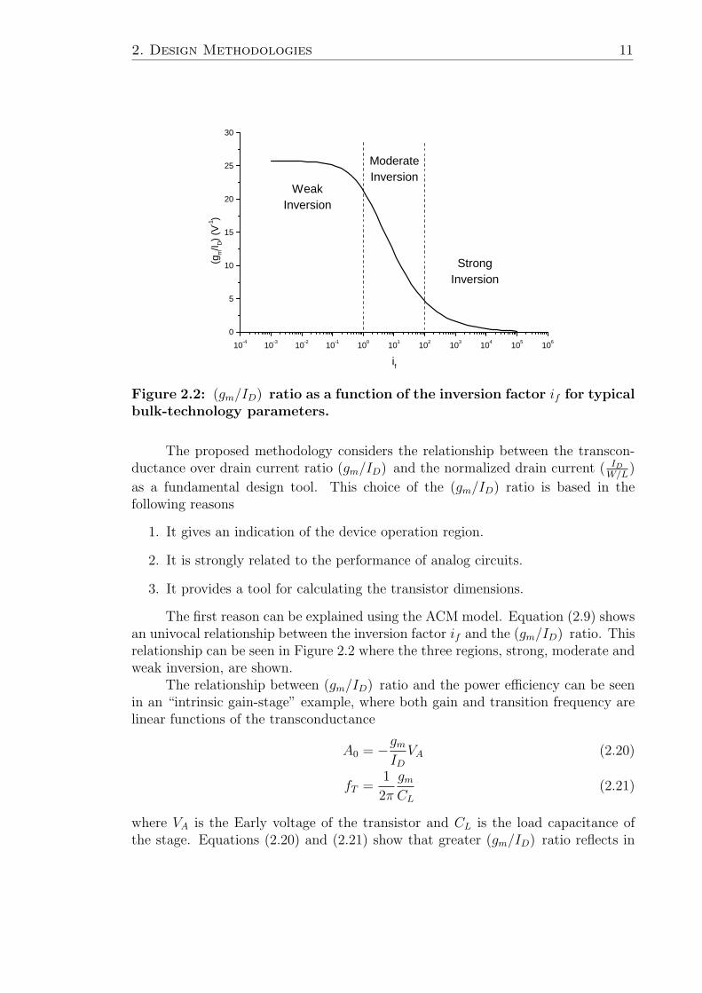
Figure 2.2: (gm/ID) ratio as a function of the inversion factor if for typicalbulk-technology parameters.
The proposed methodology considers the relationship between the transcon-ductance over drain current ratio (gm/ID) and the normalized drain current ( ID
W/L)
as a fundamental design tool. This choice of the (gm/ID) ratio is based in thefollowing reasons
1. It gives an indication of the device operation region.
2. It is strongly related to the performance of analog circuits.
3. It provides a tool for calculating the transistor dimensions.
The first reason can be explained using the ACM model. Equation (2.9) showsan univocal relationship between the inversion factor if and the (gm/ID) ratio. Thisrelationship can be seen in Figure 2.2 where the three regions, strong, moderate andweak inversion, are shown.
The relationship between (gm/ID) ratio and the power efficiency can be seenin an “intrinsic gain-stage” example, where both gain and transition frequency arelinear functions of the transconductance
A0 = −gm
ID
VA (2.20)
fT =1
2π
gm
CL
(2.21)
where VA is the Early voltage of the transistor and CL is the load capacitance ofthe stage. Equations (2.20) and (2.21) show that greater (gm/ID) ratio reflects in

12 2.4 Automatic Synthesis for Miller Amplifiers
greater gain and bandwidth for the same power consumption.Finally, the ability to precisely obtain transistors dimension with this metho-
dology lays in the fact that the (gm/ID) vs ID/(W/L) characteristic is independentof transistor size, and therefore is a unique characteristic for all transistors of thesame type in a given batch [1].
This “universal” quality of the (gm/ID) curve shows that once a pair of valuesamong (gm/ID), gm and ID are chosen, (W/L) ratio is unambiguously determined[1].
2.4 Automatic Synthesis for Miller AmplifiersIn this section an automatic synthesis algorithm for Miller amplifiers is presen-
ted. This will illustrate the use of the (gm/ID) methodology applied in automaticcircuit synthesis.
First the Miller Amplifier is analyzed and the equations that characterize itsbehavior are presented. Then the concept of design space exploration for optimumdesign is presented. The design space exploration in the case of the Miller amplifier isimplemented with a gain-bandwidth product driven algorithm that is also explainedin this section.
Finally, two amplifiers will be synthesized, each for a different transition fre-quency. The first for fT = 100kHz and the second for fT = 50MHz.
2.4.1 The Miller Amplifier
The Miller compensated amplifier is a well known opamp architecture that canachieve good power consumption performances in low frequency applications. Figure2.3 shows the amplifier schematic, where Cm is the Miller compensating capacitance,C1, Cout and C3 are parasitic capacitances and CL is the load capacitance. In thenotation used, C2 = Cout + CL is the total output capacitance of the amplifier.
Gain-Bandwidth Product and Phase Margin
The transfer function of this amplifier is given in equation (2.22), wheregm1(gm2) is the transconductance of, respectively, the differential pair M1a−M1b(output stage M2) and g1 (g2) is the output conductance of the first stage (secondstage).
H(s) = −gm1(Cms− gm2)
1g1
1g2
1 + (C1
g1+ C2
g2+ Cm( gm2
g1g2+ 1
g1+ 1
g2))s + (C1C2+Cm(C1+C2)
g1g2)s2
(2.22)

2. Design Methodologies 13
Figure 2.3: Miller Amplifier, including parasitics capacitances.
DC gain and expressions of poles and zero frequencies can be easily derived fromequation (2.22)
G =gm1gm2
g1g2
(2.23)
ωDP ' 1gm2
g1g2Cm
(2.24)
ωNDP ' gm2Cm
C1C2 + Cm(C1 + C2)(2.25)
ωz =gm2
Cm
(2.26)
where G is the DC gain, ωDP and ωNDP are the amplifier’s dominant and non-dominant pole angular frequencies and ωz is the amplifier right-half plane zero an-gular frequency3.
Equations (2.23-2.26) can be used to obtain the following relationships
ωT = GωDP =gm1
Cm
(2.27)
NDP =ωNDP
ωT
=gm2
gm1
C2m
C1C2 + Cm(C1 + C2)(2.28)
Z =ωz
ωT
=gm2
gm1
(2.29)
where ωT is the gain-bandwidth product of the first order system neglecting the effect
3In what follows, angular frequencies (ω) will be referred in the text, for compactness, asfrequencies, while the actual frequencies will be noted as f
14 2.4 Automatic Synthesis for Miller Amplifiers
of the non-dominant pole. NDP and Z are the non-dominant pole and right-halfplane zero frequencies normalized to ωT . These two latter relationships determinethe phase margin (PM) of the amplifier. Assuming NDP, Z > 1 (that is ωNDP , ωz >ωT ), PM can be approximated as
PM = 90− arctan(1
NDP)− arctan(
1
Z) (2.30)
The exact PM expression must take into account that the actual transistorsfrequency is different from the first order approximation.
Finally, equations (2.28) and (2.29) can be combined to obtain an expressionfor the Miller compensating capacitance for a given NDP over Z ratio.
Cm =1
2
NDP
Z
[C1 + C2 +
√(C1 + C2)2 + 4
Z
NDPC1C2
](2.31)
Since NDP and Z ratios determine the phase margin of the amplifier, as we sawin equation (2.30), equations (2.27) and (2.31) become powerful design tools in aMiller amplifier synthesis.
Offset
Two effects will be considered in the input offset voltage of a Miller ampli-fier: systematic offset and random offset. The first one is due to the finite outputimpedance of the current mirror (M3a − b). The second one is due to the mis-match between the mirror transistors and the mismatch between the differentialpair transistors.
Systematic Offset, as we said, is due to the finite output impedance of thecurrent mirror. When there is a difference between the drain-source voltage of eachmirror transistor, a difference appears between the drain currents. The relative errorin the copy can be estimated as
∆ID
ID
=1
ID
∆V
ro
=∆V
VA
(2.32)
where ∆V = VDS3a − VDS3b, ro = VA/ID is the output resistance of the mirrortransistors and VA is the Early voltage. The offset voltage due to this copy errorcan be calculated through the differential pair transconductance as
Voff =∆ID
gm
=∆ID/ID
(gm/ID)=
∆V/VA
(gm/ID)(2.33)
which is a useful expression as it estimates the systematic offset voltage as a functionof the (gm/ID) ratio of the differential pair.
Random Offset is due to the mismatch between the transistors of the mirrorand the mismatch between the transistors of the differential pair. To model these
2. Design Methodologies 15
mismatches the following analysis is made. Current through a forward saturatedtransistor can be expressed as a function of the current factor (β = µC ′
oxW/L), thethreshold voltage (VT0) and the gate voltage. As gate voltage is the same for bothtransistors, either in the mirror or in the differential pair, the current error can bewritten as
ID − ID = ∆ID =∂ID
∂VT0
∆VT0 +∂ID
∂β∆β (2.34)
where ID is the mean current value and ID is the actual current value of each sample.The partial derivatives can be approximated as
∂ID
∂VT0
=∂ID
∂VG
∂VG
∂VT0
= gm · 1 = gm (2.35)
∂ID
∂β=
ID
β(2.36)
allowing us to rewrite equation (2.34) as
∆ID = gm∆VT0 +ID
β∆β (2.37)
The standard deviation of the current will depend on the standard deviationof VT0 and β. Since this two random effects are considered statistically independent,the standard deviation of the current is
σID
ID
=
√(gm
ID
)2
σ2VT0
+σ2
β
β2(2.38)
where the standard deviation of VT0 and β (σ2VT0
, σ2β) can be expressed using Pel-
grom’s model [36]:
σ2VT0
=A2
VT0
W.L+ S2
VT0D2 (2.39)
σ2β
β2=
A2β
W.L+ S2
βD2 (2.40)
Here D represents the distance between transistors and depends strongly on transis-tor’s layout and size. When considering transistors with an almost square structure,D can be approximated as D =
√WL [3]. Finally, Aβ, AVT0
, SVT0and Sβ are the
coefficients that characterize the matching properties in a particular process andcan be obtained from the foundry itself or from published results on matching.
Taking transistor’s mismatch on the mirror and the differential pair as statis-tically independent, total current error can be expressed as
σID
ID
=
√(σID
ID
)2
pair
+
(σID
ID
)2
mirr
(2.41)

16 2.4 Automatic Synthesis for Miller Amplifiers
0 5 10 15 20 250
1
2
3
4
5
6
7
8
9
10
11
12
13Mirror:
(gm/ID)=10 V-1
W/L = 18/9∆V = 200 mV
Diff. Pair:W/L = 18/3
Pelgrom model:AVTo=30 mVµmSVTo=4 µV/µmAβ=2.3 %µm
Sβ=2x10⁻⁴ %/µm
Total Matching Systematic
Offs
et V
olta
ge
(m
V)
gm/I
D (V-1)
Figure 2.4: Offset voltage in a differential pair with active load as afunction of (gm/ID)pair .
which gives a total mismatch offset
Voff =σID
/ID
(gm/ID)pair
(2.42)
Equations (2.38)-(2.42) conform a useful set to easily estimate the input offset vol-tage due to transistor mismatch in the amplifier.
Figure 2.4 shows an example where the offset voltage is evaluated as a functionof the (gm/ID) ratio of the differential pair for given transistors sizes and mirror’s(gm/ID) ratio. Here we can see that a steep decrease in the offset voltage appears aswe move from strong to moderate inversion. As we enter into deep weak inversionthe offset voltage tends to a constant value. It can be seen also that generally,systematic offset is much smaller than mismatch offset. Similar and further analysison the effect of the (gm/ID) ratio on mirror precision and OTA’s offset voltage canbe found on [3].
Input Common Mode Range and Output Swing
Input Common Mode Range (ICMR) and Output Swing (OS) can be easilyestimated using the equations provided by the ACM model for saturation voltage(VDSsat, equation (2.8)) and gate voltages (equation (2.7)).
ICMR is determined by the saturation voltage of the differential pair’s currentsource (M5) and the gate voltage of the mirror (M3a− b, see Figure 2.3).
VSS + VGS3 + VDSsat1 − VGS1 < ViCM < VDD − VDSsat5 − VGS1 (2.43)

2. Design Methodologies 17
Output Swing, on the other hand is determined by the saturation voltagesof the output stage transistors (M2 and M4, see Figure 2.3).
VSS + VDSsat2 < V o < VDD − VDSsat4 (2.44)
2.4.2 Gain-Bandwidth Driven Synthesis Algorithm
The basic synthesis algorithm for the Miller amplifier that will be applied here,was presented by Jespers [2]. The main idea is to synthesize a Miller amplifier for agiven gain-bandwidth product ωT and a given phase margin (PM). The rest of theperformance specifications (DC gain, SR, noise, etc.) are adjusted by the selectionof the design variables ((gm/ID) ratios and lengths).
The designer chooses the (gm/ID) ratio of each stage (that is the (gm/ID)ratio of the differential pair transistors and the (gm/ID) ratio of transistor M2)taking into consideration, for example, the objective gain-bandwidth product andthe current budget available. Also, the length of the transistors is selected accordingto noise, gain and matching considerations. NDP and Z ratios can be chosen for agiven objective phase margin. For example, it is common to take NDP = 2.2 andZ = 10 to achieve PM ' 60o.4
Then using equations (2.27) and (2.31) and applying the (gm/ID) methodo-logy, transistors sizes and other parameters (DC gain, SR, noise, etc.) can beobtained.
The basic algorithm, as presented by Jespers is shown in Algorithm 2.1. In thisalgorithm, there are some missing design criteria. Step 4 (Algorithm 2.1) establishesmirror design to minimize offset. This is one of the choices, but noise, frequencyresponse or gain could be used jointly with or instead of this criterium. On step 5(Algorithm 2.1), the design criterium for the (gm/ID) ratio isn’t even specified. Insection 2.4.4 the criterium used in this work is explained.
2.4.3 Design Optimization Through Design Space Exploration
In Algorithm 2.1, (gm/ID) ratios and lengths must be selected a priori by thedesigner. However, this may not be an easy task for an unexperienced user and canlead to very non-optimum designs.
To obtain an optimum design, we can define a design space by both stage’sactive transistors (gm/ID) ratios and explore the characteristics of the amplifieron it. This may be achieved applying Algorithm 2.1 in a mesh of points for thedefined design space. In this way constant-level curves for every aspect of theamplifier required by the designer can be plotted to graphically show the behaviorof the amplifier in the design space. This idea is based on the (gm/ID) based
4Actually, since NDP and Z are normalized to ωT of the first order system approximation, wecould expect that the real PM will be bigger. However, other effects present in the real amplifier,as the pole-zero doublet from the input stage mirror, will eventually have a negative impact onthe PM, leading to actual PM of about 60o.
18 2.4 Automatic Synthesis for Miller Amplifiers
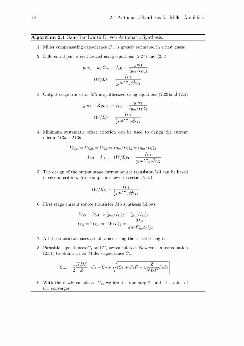
Algorithm 2.1 Gain-Bandwidth Driven Automatic Synthesis.
1. Miller compensating capacitance Cm is grossly estimated in a first guess.
2. Differential pair is synthesized using equations (2.27) and (2.5)
gm1 = ωT Cm ⇒ ID1 =gm1
(gm/ID)1
(W/L)1 =ID1
12µnC ′
oxφ2t if1
3. Output stage transistor M2 is synthesized using equations (2.29)and (2.5)
gm5 = Zgm1 ⇒ ID2 =gm2
(gm/ID)2
(W/L)2 =ID2
12µnC ′
oxφ2t if2
4. Minimum systematic offset criterion can be used to design the currentmirror M3a−M3b
VG3a = VD3b = VG2 ⇒ (gm/ID)3 = (gm/ID)2
ID3 = ID1 ⇒ (W/L)3 =ID1
12µnC ′
oxφ2t if2
5. The design of the output stage current source transistor M4 can be basedin several criteria. An example is shown in section 2.4.4.
(W/L)4 =ID2
12µnC ′
oxφ2t if4
6. First stage current source transistor M5 synthesis follows
VG5 = VG4 ⇒ (gm/ID)5 = (gm/ID)4
ID5 = 2ID1 ⇒ (W/L)5 =2ID1
12µnC ′
oxφ2t if4
7. All the transistors sizes are obtained using the selected lengths.
8. Parasitic capacitances C1 and C2 are calculated. Now we can use equation(2.31) to obtain a new Miller capacitance Cm
Cm =12
NDP
Z
[C1 + C2 +
√(C1 + C2)2 + 4
Z
NDPC1C2
]
9. With the newly calculated Cm we iterate from step 2, until the value ofCm converges.

2. Design Methodologies 19
Algorithm 2.2 Power Optimization Automatic Synthesis
1. The length of all transistors is set to minimum.
2. (gm/ID)4 ratio is fixed somewhere in moderate inversion.
3. The design space is swept using Algorithm 2.1. We choose the optimumcombination of input and output stage (gm/ID) ratio.
4. The length of M3 is swept. We choose L3 to obtain good gain and frequencyresponse.
5. (gm/ID)4 ratio is swept. We choose it to obtain good Output Swing andtotal area.
6. The length of M4 is swept. We choose L4 to obtain good gain and totalarea. We iterate with step 5 until we converge to a solution for both(gm/ID)4 and L4.
7. We run Algorithm 2.1 with the values obtained for (gm/ID) ratios and L′s.
methodology [1], explained in section 2.3, and has been used in previous works( [2, 3]).
Doing so, not only optimum combinations of the (gm/ID) ratios can be ob-tained, but also the evolution of the aspect under study can be evaluated. Thismeans that we may consider several aspects of the amplifier and select an optimumcombination of the (gm/ID) ratios in a multi-aspect sense.
Lengths and non-critical (gm/ID) ratios (e.g. second stage bias transistor) canalso be selected using similar methodology. For example, a sweep of the length ofmirror transistors can be used to select an optimum trade-off between frequencyresponse and gain.
Applying these ideas, we developed an algorithm that explores the designspace of the Miller amplifier to obtain optimum consumption with good gain andarea. thus, the algorithm also analyzes the effects of lengths and passive transistor’s(gm/ID) ratios to consider the trade-offs in the performance of the amplifier.
This algorithm is presented in Algorithm 2.2 and in sections 2.4.4 and 2.4.5we present two design examples. The algorithm is explained thoroughly when thefirst example is introduced in section 2.4.4.
2.4.4 Synthesis Example: Micropower 100kHz Miller Amplifier
Table (2.1) shows the specifications for the design of this first example. As itcan be seen, this design is intended for low frequency, low supply voltage, micropoweroperation. The process parameters are taken from a 0.8µm technology.
First, the initial conditions for the algorithm (steps 1 and 2) are set. Thelength of the transistors can be latter adjusted to improve gain and (gm/ID)4 wasset to 10. We then sweep the design space to obtain constant consumption, area

20 2.4 Automatic Synthesis for Miller Amplifiers
fT 100kHzConsumption < 1µAPower Supply 2V
CL 10pFPM > 60
Tech. 0.8µm
Table 2.1: Specifications for a Micropower 100kHz Miller Amplifier
6 8 10 12 14 16 18 20 22 24 26
6
8
10
12
14
16
18
20
22
24
(gm/ID)1
(gm
/ID) 2
0.9
0.9
0.9
1
1
1
1
1.2
1.2
1.21.2
1.4
1.4
1.4
1.4 1.4
1.6
1.61.6 1.6
1.8
1.81.8
2.1
2.1 2.12.42.4 2.42.82.8 2.83.2
O Minimum Consumption
Figure 2.5: Design space exploration: Total consumption (in µA) of the100kHz Miller Amplifier.
and dc gain curves.Figures 2.5, 2.6 and 2.7 show the space exploration for consumption, area and
dc gain respectively. They clearly show that optimum consumption with reasonablegain and die area can be obtained when both stage’s active transistors are in weakinversion. Particulary we choose:
(gm/ID)1 = 24
(gm/ID)2 = 22
The lengths of the differential pair transistors and output stage active transis-tor are chosen 3µm to avoid big sizes, but at the same time obtain a good gain.
Mirror’s transistors can be designed according to several criteria. As shown inAlgorithm 2.1 (step 4) we choose to minimize the systematic offset of the amplifier.As seen in section 2.4.1, systematic offset is due to a difference in the drain-source

2. Design Methodologies 21
6 8 10 12 14 16 18 20 22 24 26
6
8
10
12
14
16
18
20
22
24
(gm/ID)1
(gm
/ID) 2
9200
9200
9200
9200
95009500
9500
9500 9500
9500
1000010000
10000
10000
10000 10000
1000
0
1100
0
1100011000 11000
11000
11000 11000
1100
0
12000
12000 12000
12000
12000 12000
1200
0
1500015000
15000 15000 15000
20000
Minimum Area O
Figure 2.6: Design space exploration: Die area estimation (in µm2) ofthe 100kHz Miller Amplifier..
6 8 10 12 14 16 18 20 22 24 26
6
8
10
12
14
16
18
20
22
24
(gm/ID)1
(gm
/ID) 2
98100
100
100
102
102
102
104 104
104
104
106 106
106
106
108
108
108
110
110
112
112
114
Figure 2.7: Design space exploration: DC Gain (in dB) of the 100kHzMiller Amplifier..

22 2.4 Automatic Synthesis for Miller Amplifiers
voltage of both transistors. Thus it can be minimized if both voltages are designedto be the same, which can be achieved using the same (gm/ID) ratio than transistorM2. Now, we only need to choose the length of both transistors. To do so, we willconsider two effects of the length in the amplifier’s behavior: gain and frequencyresponse (step 4).
The effect on gain, lays on the fact that the output resistance of the transistorscan be modelled to be proportional to the length through the Early voltage (ro =VA/ID, VA = VEL). Regarding, the frequency response, a given (gm/ID) ratio anddrain current fix the W/L ratio. That means that larger length implies larger widthand, thus, larger parasitic capacitance (which depends grossly on W and on theWL product). Since the parasitic capacitance C3 adds a pole-zero doublet to theresponse of the Miller amplifier [37], the length of the mirror transistors also has aneffect on the frequency response. This doublet has a small impact on the frequencyresponse but a large one on the transient response and should be kept beyond theworking frequencies.
ωpDOUB =gm3
C3
(2.45)
ωzDOUB =2gm3
C3
(2.46)
Both effects can be seen on Figure 2.8 where the doublet frequency is calculatedusing equation (2.45). The improvement on the gain starts to diminish as a longertransistor is selected, because for L3 À L1 the gain is determined only by L1. Thus,in this design we choose:
L3 = 9µm (2.47)
which gives a good gain and a doublet frequency almost a decade above the transitionfrequency.
The design criteria for the output stage bias transistor (M4) wasn‘t specified onAlgorithm 2.1. We choose to select its (gm/ID) ratio and length with the followinganalysis (steps 5 and 6). The design of transistor M4 affects gain, total area (likeany transistor) and output swing. Length will affect gain and area (eqs. 2.49 and2.50) and (gm/ID) ratio will affect area and output swing (eqs. 2.48 and 2.49).
VDSsat = f ((gm/ID) ) ⇒ OS = f ((gm/ID) ) (2.48)(W
L
)= f ((gm/ID) ) ⇒ Area = f ((gm/ID) , L4) (2.49)
Gain = f (g4 + g2) ⇒ Gain = f (L4) (2.50)
where g4, g2 are the output conductance of transistors M4,M2 respectively.Figure 2.9 shows the dependence of the output swing and total area with
(gm/ID)4 . In this figure we see that the output swing behaves, as expected, accor-ding to the relationship between VDSsat and (gm/ID) ratio seen on equation (2.8).This behavior shows that there is no reason to go into deep weak inversion because

2. Design Methodologies 23
1 10 100
104
106
108
110
112
114
116
Gain
Ga
in (
dB
)
L3 (µm)
1 10 100
10k
100k
1M
10M
Fre
qu
en
cy (Hz)
Doublet f
T
Figure 2.8: Gain and doublet frequency dependence on the length of M3.
0 5 10 15 20 25
103
104
105
106
VDD
= 1VV
SS = -1V
Area
Are
a (
µm2 )
(gm/ID)4
0,2
0,3
0,4
0,5
0,6
0,7
0,8
0,9
1,0
Upper Output Swing Limit
Vo (M
ax) (V
)
Figure 2.9: Output swing and total area dependence on (gm/ID)4 ratio.

24 2.4 Automatic Synthesis for Miller Amplifiers
1 10 100 1000
104
105
AreaA
rea
(µm
2 )
L4 (µm)
106
108
110
112
114
Gain
Ga
in (d
B)
Figure 2.10: Gain and total area dependence on the length of M4.
no further increase on the output swing is achieved. What is more, the total areastarts to raise exponentially as we move beyond (gm/ID)4 > 10. Thus, we choose
(gm/ID)4 = 6
which gives an upper output swing limit of 0.7V (power supply: ±1V ) and a totalarea of about 104µm2.
Figure 2.10 shows the dependence of the gain and total area with L4. As withthe case of transistor M3, increasing the length improves the gain, but only to someextent. We choose
L4 = 60µm
which gives a good gain and a total area of about 104µm2.
Final Design
The final design obtained (step 7) can be seen on Table (2.2). Here we seethat, as expected, the frequency response isn’t fully achieved due to the presenceof higher order effects like the mirror pole-zero doublet. Systematic offset is effecti-vely eliminated, as simulation showed that drain-source voltage difference in mirrortransistors is below 5mV . Total consumption is kept below 1µA. The ratio betweenboth stage’s bias current is due to factor Z (equation (2.29)). It can be easily seenthat for the same (gm/ID) ratios the currents ratio equals Z. A more efficient ar-chitecture is obtained when using a R-C compensating network that eliminates theright-half plane zero.
This design was simulated on SPICE using the BSIM3v3 transistor model.
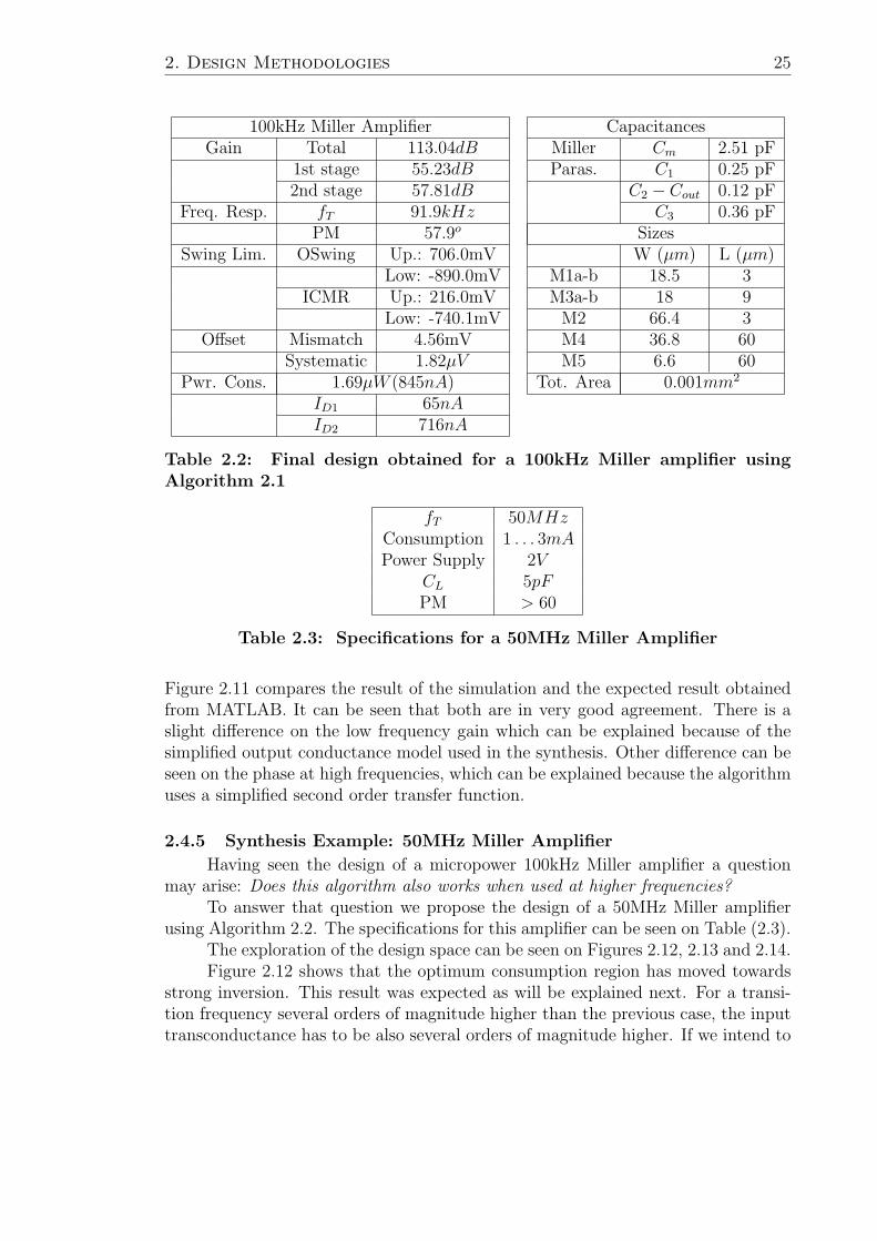
2. Design Methodologies 25
100kHz Miller Amplifier CapacitancesGain Total 113.04dB Miller Cm 2.51 pF
1st stage 55.23dB Paras. C1 0.25 pF2nd stage 57.81dB C2 − Cout 0.12 pF
Freq. Resp. fT 91.9kHz C3 0.36 pFPM 57.9o Sizes
Swing Lim. OSwing Up.: 706.0mV W (µm) L (µm)Low: -890.0mV M1a-b 18.5 3
ICMR Up.: 216.0mV M3a-b 18 9Low: -740.1mV M2 66.4 3
Offset Mismatch 4.56mV M4 36.8 60Systematic 1.82µV M5 6.6 60
Pwr. Cons. 1.69µW (845nA) Tot. Area 0.001mm2
ID1 65nAID2 716nA
Table 2.2: Final design obtained for a 100kHz Miller amplifier usingAlgorithm 2.1
fT 50MHzConsumption 1 . . . 3mAPower Supply 2V
CL 5pFPM > 60
Table 2.3: Specifications for a 50MHz Miller Amplifier
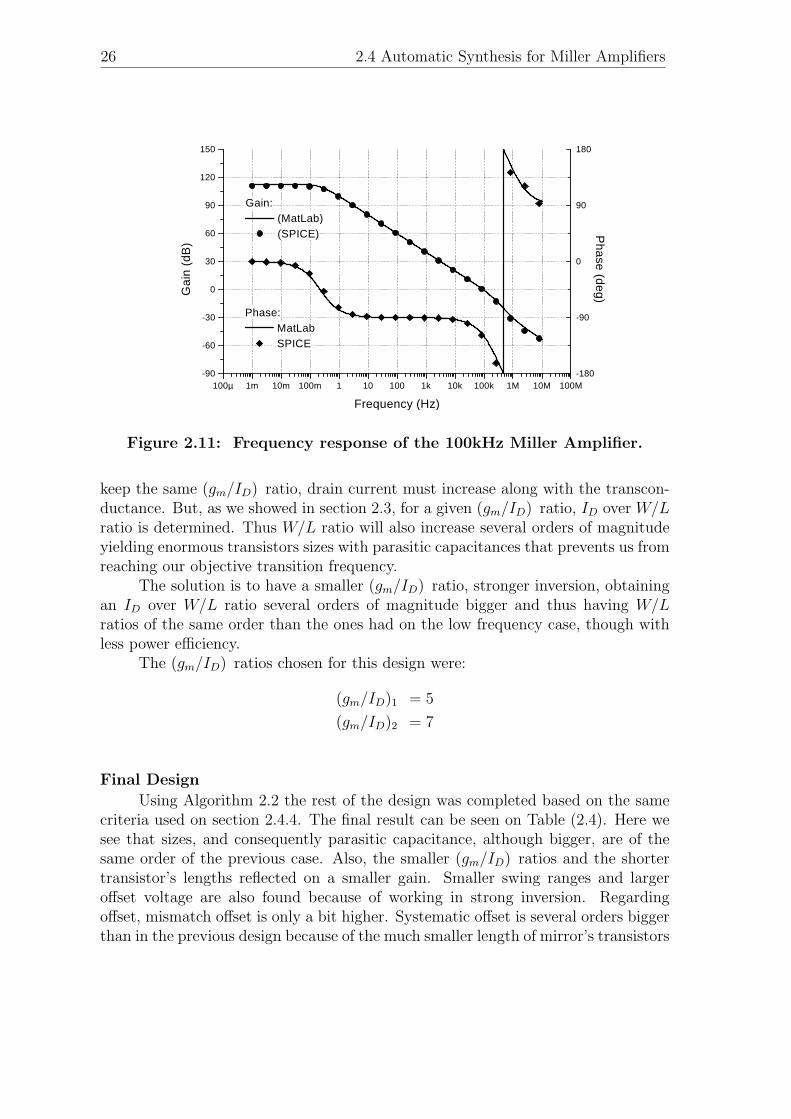
Figure 2.11 compares the result of the simulation and the expected result obtainedfrom MATLAB. It can be seen that both are in very good agreement. There is aslight difference on the low frequency gain which can be explained because of thesimplified output conductance model used in the synthesis. Other difference can beseen on the phase at high frequencies, which can be explained because the algorithmuses a simplified second order transfer function.
2.4.5 Synthesis Example: 50MHz Miller Amplifier
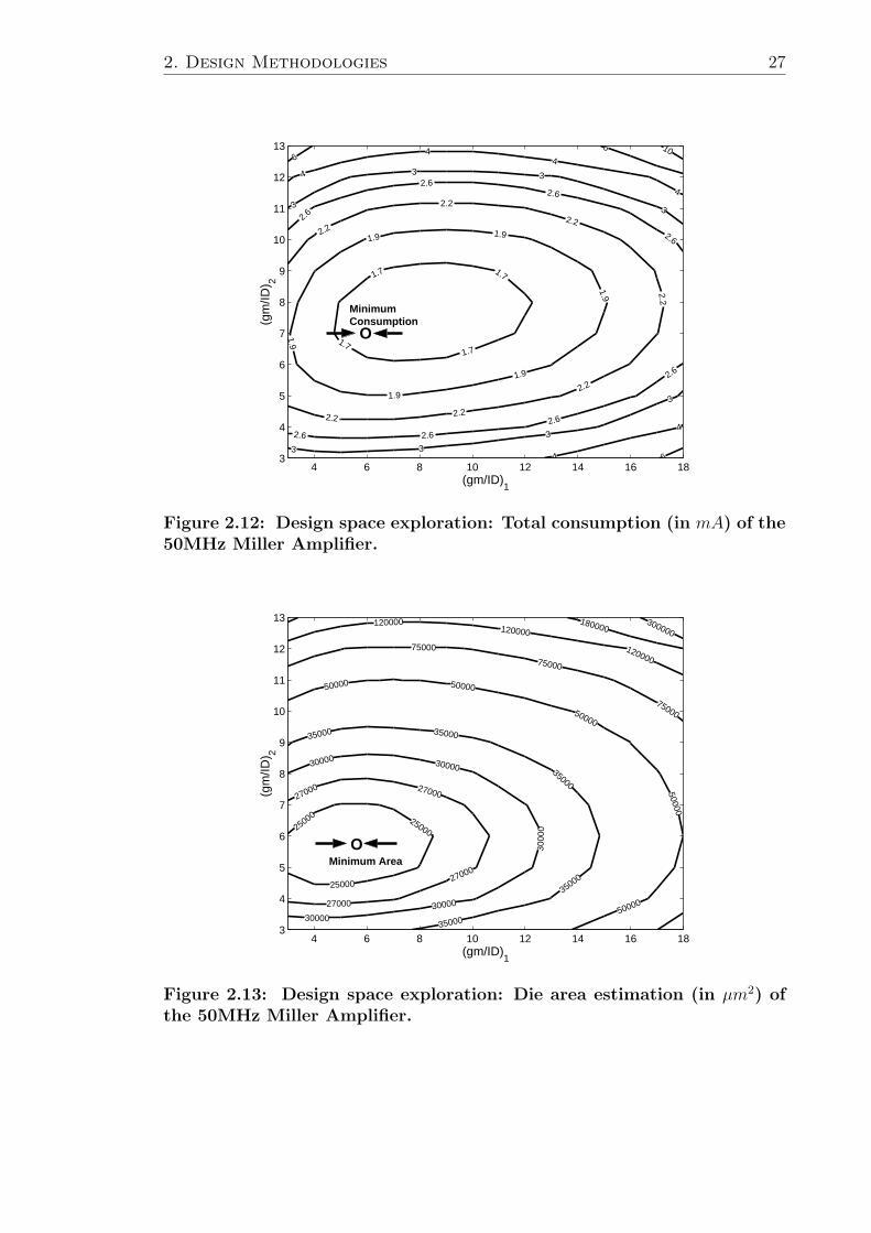
Having seen the design of a micropower 100kHz Miller amplifier a questionmay arise: Does this algorithm also works when used at higher frequencies?
To answer that question we propose the design of a 50MHz Miller amplifierusing Algorithm 2.2. The specifications for this amplifier can be seen on Table (2.3).
The exploration of the design space can be seen on Figures 2.12, 2.13 and 2.14.Figure 2.12 shows that the optimum consumption region has moved towards
strong inversion. This result was expected as will be explained next. For a transi-tion frequency several orders of magnitude higher than the previous case, the inputtransconductance has to be also several orders of magnitude higher. If we intend to
26 2.4 Automatic Synthesis for Miller Amplifiers
100µ 1m 10m 100m 1 10 100 1k 10k 100k 1M 10M 100M-90
-60
-30
0
30
60
90
120
150
Gain: (MatLab) (SPICE)
Ga
in (
dB
)
Frequency (Hz)
-180
-90
0
90
180
Ph
ase
(de
g)
Phase: MatLab SPICE
Figure 2.11: Frequency response of the 100kHz Miller Amplifier.
keep the same (gm/ID) ratio, drain current must increase along with the transcon-ductance. But, as we showed in section 2.3, for a given (gm/ID) ratio, ID over W/Lratio is determined. Thus W/L ratio will also increase several orders of magnitudeyielding enormous transistors sizes with parasitic capacitances that prevents us fromreaching our objective transition frequency.
The solution is to have a smaller (gm/ID) ratio, stronger inversion, obtainingan ID over W/L ratio several orders of magnitude bigger and thus having W/Lratios of the same order than the ones had on the low frequency case, though withless power efficiency.
The (gm/ID) ratios chosen for this design were:
(gm/ID)1 = 5
(gm/ID)2 = 7
Final Design
Using Algorithm 2.2 the rest of the design was completed based on the samecriteria used on section 2.4.4. The final result can be seen on Table (2.4). Here wesee that sizes, and consequently parasitic capacitance, although bigger, are of thesame order of the previous case. Also, the smaller (gm/ID) ratios and the shortertransistor’s lengths reflected on a smaller gain. Smaller swing ranges and largeroffset voltage are also found because of working in strong inversion. Regardingoffset, mismatch offset is only a bit higher. Systematic offset is several orders biggerthan in the previous design because of the much smaller length of mirror’s transistors
2. Design Methodologies 27
4 6 8 10 12 14 16 183
4
5
6
7
8
9
10
11
12
13
(gm/ID)1
(gm
/ID) 2
1.71.7
1.71.7
1.9
1.9
1.9
1.9
1.91.92.2
2.2
2.22.2
2.2
2.22.2
2.6
2.62.6
2.6
2.6 2.6
2.6
2.6
3
3 3
3
3 3
3
3
4
4
4
44
4
66
6
10
O
Minimum Consumption
Figure 2.12: Design space exploration: Total consumption (in mA) of the50MHz Miller Amplifier.
4 6 8 10 12 14 16 183
4
5
6
7
8
9
10
11
12
13
(gm/ID)1
(gm
/ID) 2
25000 25000
25000
27000 27000
27000
27000
30000 30000
3000
0
30000
3000035000
35000
35000
3500035000
50000
50000
50000
5000050000
75000
75000
75000
120000120000
120000
180000300000
O Minimum Area
Figure 2.13: Design space exploration: Die area estimation (in µm2) ofthe 50MHz Miller Amplifier.

28 2.4 Automatic Synthesis for Miller Amplifiers
4 6 8 10 12 14 16 183
4
5
6
7
8
9
10
11
12
13
(gm/ID)1
(gm
/ID) 2
55 60
6065
65
65
65
70
70
70
70
75
75
75
80
Figure 2.14: Design space exploration: Total gain (in dB) of the 50MHzMiller Amplifier.
50MHz Miller Amplifier CapacitancesGain Total 63.8dB Miller Cm 2.93 pF
1st stage 28.0dB Paras. C1 1.53 pF2nd stage 35.8dB C2 − Cout 2.72 pF
Freq. Resp. fT 46.1MHz C3 0.48 pFMF 58.9o Sizes
Swing Lim. OSwing Up.: 591 mV W (µm) L (µm)Low: -764 mV M1a-b 109 1
ICMR Up.: -297 mV M3a-b 77.4 0.8Low: -599 mV M2 691 1
Offset Mismatch 6.36 mV M4 1431 3Systematic 0.10mV M5 401 3
Pwr. Cons. 3.36mW (1.68mA) Tot. Area 0.025mm2
ID1 184µAID2 1.31mA
Table 2.4: Final design obtained for a 50MHz Miller amplifier usingAlgorithm 2.1

2. Design Methodologies 29
100 1k 10k 100k 1M 10M 100M 1G 10G 100G-80
-60
-40
-20
0
20
40
60
80
Gain: MatLab SPICE
Ga
in (
dB
)
Frequency (Hz)
-180
-90
0
90
180P
ha
se (d
eg
)
Phase: MatLab SPICE
Figure 2.15: Frequency response of the 50MHz Miller Amplifier.
and the stronger inversion operation. The criterium used still stands as drain-sourcevoltage difference stays in the vicinity of only some mV . Finally, GBW product andPM are, again, a bit lower than requirements due to higher order terms.
Figure 2.15 shows the same comparison made in section 2.4.4 between theMATLAB estimation of the frequency response and the SPICE simulation. Here,again, we found that the main difference appears at low frequencies where we useda simple output conductance model to estimate frequency response in MATLAB.
2.5 ConclusionsThis chapter presented the reader with the ACM transistor model and its
equations that will be used through out this work. The advantages of this modelfor automatic synthesis were also reviewed.
We then introduced the concept of design space exploration using the (gm/ID)methodology [1]. This is a keystone in the further development of automatic synt-hesis algorithms. The design space exploration allows to have a graphical represen-tation of the evolution of a desired characteristic (consumption, area, dc gain, noise,etc.) with the design variables defined, for example in the case of a Miller amplifier,by the (gm/ID) ratios of the active transistors of each stage.
To show these ideas we present two different designs of a two-stage Milleroperational amplifier using a gain-bandwidth driven algorithm. With this algorithmwe obtained design space exploration plots for consumption, area and dc gain in eachdesign which allowed us to design the amplifiers, in this case, for optimum powerconsumption. Examples of how to apply the (gm/ID) methodology and the ideaof design space exploration were also used to optimize non-critical parameters as

30 2.5 Conclusions
transistors lengths or current sources (gm/ID) ratios.Excellent agreement between the calculated performance and the simulations
made, validates the methodology and allow us to step further into more advanceautomatic synthesis methodology for more complex opamps architectures.

Chapter 3Low-Power OpAmp Cells: Reuse, Architecture
and Synthesis
3.1 IntroductionOn Chapter 2 we reviewed the basic ideas in automatic synthesis algorithms.
Design space exploration using the (gm/ID) methodology [1] proved to be an effec-tive tool to automatically obtain minimum power designs.
On this Chapter, we will first explore the possibility of analog design reuse.Section 3.2 will review this idea from three points of view: Circuit performancetuning, Architectures and Technology migration. Then on section 3.3, we will reviewthe architecture selected to be used on the amplifier to be designed in Chapter 4.This architecture complies with the reusability characteristics described in section3.2.
Then, on section 3.4 we will present an example of advanced design metho-dology. Particulary, we will present an algorithm that systematically transits fromhigh level specifications of the amplifier (e.g. total settling time), towards a low leveldesign that complies with the high level specifications with minimum power con-sumption [3]. This algorithm will be partially modified in Chapter 4 to be used in ahierarchical automatic synthesis algorithm used in the design of the much complexarchitecture presented in section 3.3.
3.2 Analog Design ReuseThe advent of deep submicron processes has enabled the system-on-chip (SOC)
design and enlarged the existing gap between design complexity and designers pro-ductivity. Time-to-market pressure makes this gap more challenging, and conse-quently, the reuse of circuit designs has become an essential tool. The urge forimplementing reuse capabilities is particularly intense in the analog field [12], sinceautomatic synthesis of analog circuits is a much hard problem than for the digitalcounterparts.
This problem is of particular interest in the Microelectronics Group of the Ins-tituto de Ingenierıa Electrica (IIE) from the Universidad de la Republica, Uruguay.Being a small research group which has to handle several projects, the possibility ofreusing analog cells in the designs we develop is a main concern, since we lack thedesigner time to implement every cell in each new project.
On this section we will study analog reuse applied to amplifiers from threepoints of view. First we will review the possibility of reusing the same design indifferent applications by tuning its performance through the reference bias current.Second we will see architectures for input and output stages that are suitable to be
31

32 3.2 Analog Design Reuse
used on different environmental conditions. And last, we will address the issue ofautomatic redesign in technology migration.
3.2.1 Circuit Performance Tuning Through Bias Current
One possible reuse scheme is to apply the reference bias current as an adjust-ment parameter to tune an existing circuit performance to suit different applica-tions and hence save design time. This approach is being address by our researchgroup [9], but also has been applied in commercial applications [4]. However, asfar as we know, all these previous applications of performance tuning in standardcircuits, has been made on bipolar technology.
Bias current can be used to tune the performance of an already fabricatedcircuit, with almost no loss of performance, based essentially on the exponentialdependence of current on voltage in weak and moderate inversion regions. Thisexponential relationship has two main consequences, the gate voltage has a very lowdependence on current (equation (2.7)) and the (gm/ID) versus ID curve is almostflat (Figure 2.2).
Using equations from section 2.4.1 we can see that a Miller amplifier operatingbetween weak inversion and moderate inversion will have a speed versus consumptiontrade-off tuned by the amplifier’s bias current while preserving acceptable operationin all other aspects (voltage swing ranges, offset, phase margin, . . .).
Gain-Bandwidth Product
Recalling equation (2.27) we see that we can tune the amplifier’s gain-bandwidthproduct adjusting the differential pair’s transconductance. In weak and near-weakinversion regions, since the (gm/ID) ratio is almost constant, the dependence of thetransconductance with bias current is linear. Hence we have a linear dependencebetween gain-bandwidth product and bias current as shown in equation (3.1) .
ωT =(gm/ID)1
Cm
ID1(gm/ID) 'cst.−−−−−−−−→ ωT ∝ ID1 (3.1)
It is worth noticing, though, that equation (2.27) is a first order approximation.Therefore it is valid as long as second order effects, related to the NDP and Z ratios,remain far enough. We will study this below, in relation to the stability margins ofthe amplifier
Figure 3.1 shows an example of tuning on the Miller amplifier designed onsection 2.4.4. Here we see how we can tune the gain-bandwidth product for severaldecades with a linear relationship with bias current and hence with total consump-tion.
We have found the way, then, to tune the performance (speed vs. consumptiontrade-off) of an existing design of our amplifier to suit different applications. Wemust now ensure that the amplifier preserves acceptable operation in other aspects.
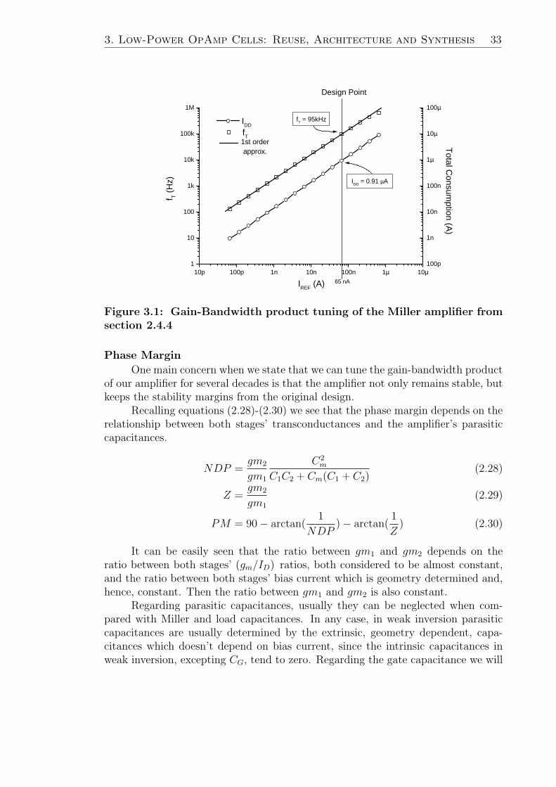
3. Low-Power OpAmp Cells: Reuse, Architecture and Synthesis 33
10p 100p 1n 10n 100n 1µ 10µ1
10
100
1k
10k
100k
1M
1st orderapprox.
65 nA
IDD = 0.91 µA
fT = 95kHz
Design Point
IREF (A)
f T (H
z)
fT
100p
1n
10n
100n
1µ
10µ
100µT
otal Consum
ption (A)
IDD
Figure 3.1: Gain-Bandwidth product tuning of the Miller amplifier fromsection 2.4.4
Phase Margin
One main concern when we state that we can tune the gain-bandwidth productof our amplifier for several decades is that the amplifier not only remains stable, butkeeps the stability margins from the original design.
Recalling equations (2.28)-(2.30) we see that the phase margin depends on therelationship between both stages’ transconductances and the amplifier’s parasiticcapacitances.
NDP =gm2
gm1
C2m
C1C2 + Cm(C1 + C2)(2.28)
Z =gm2
gm1
(2.29)
PM = 90− arctan(1
NDP)− arctan(
1
Z) (2.30)
It can be easily seen that the ratio between gm1 and gm2 depends on theratio between both stages’ (gm/ID) ratios, both considered to be almost constant,and the ratio between both stages’ bias current which is geometry determined and,hence, constant. Then the ratio between gm1 and gm2 is also constant.
Regarding parasitic capacitances, usually they can be neglected when com-pared with Miller and load capacitances. In any case, in weak inversion parasiticcapacitances are usually determined by the extrinsic, geometry dependent, capa-citances which doesn’t depend on bias current, since the intrinsic capacitances inweak inversion, excepting CG, tend to zero. Regarding the gate capacitance we will

34 3.2 Analog Design Reuse
see below that it can be considered constant when working on weak and near-weakinversion.
In conclusion both NDP and Z ratios, and thus the phase margin, remainalmost constant when tuning the gain-bandwidth product of the amplifier. On theMiller amplifier designed on section 2.4.4, the phase margin varies less than 1.8% asthe GBW is tuned over 4 decades.
Voltage Swing Ranges
Both ICMR (Input Common Mode Range) and Output Swing are determinedby gate-source voltages and drain-source saturation voltages, as shown in section2.4.1.
It has already been shown that both these voltages have low dependence onbias current when operating in weak and moderate inversion. For instance, onequation (2.8) and Figure 2.1 we see how the drain-source saturation voltage tendsto a constant minimum value when entering weak inversion operation.
Offset
In section 2.4.1 the Miller amplifier’s input offset voltage was studied. Reca-lling equation (2.41) and the preceding equations, we found that both systematicand random offset can be written as functions of the (gm/ID) ratios of the inputdifferential pair and mirror. Since the input stage mirror was designed to have thesame normalized current ratio ( ID
W/L) as the output stage active transistor, it will
also have it’s same (gm/ID) ratio over all the tuning range. Particulary we canrewrite the total input offset voltage as
Voff =
√A +
B
(gm/ID)p2
+ C(gm/ID)m
2
(gm/ID)p2
(3.2)
where A, B and C are all current independent parameters and subscript m (p)refers to mirror (differential pair). It can be easily seen, then, that the offset voltagetends to a constant value as we enter weak inversion, where both (gm/ID) ratios areconstant.
Intrinsic Capacitances
It can be seen from equation (2.12) that the total gate capacitance in a forwardsaturated transistor tends to CG = n−1
nCox when if ¿ 1, i.e. operating in weak
inversion. Reference [10] shows that all other eight intrinsic capacitances tend tozero when operating in weak inversion region, as we mentioned above.
Thus, since the slope factor n is constant and Cox is geometry dependent, theintrinsic capacitances are either negligible or constant in weak inversion.
3. Low-Power OpAmp Cells: Reuse, Architecture and Synthesis 35
Noise
Recalling equations (2.17) and (2.18)
fc ' 1
2
gm
WLC ′ox
Not
N∗ (2.17)
Si = 2nkBTgm
(1 +
fc
f
)(2.18)
we see that the total noise current through a MOS transistor depends on its trans-conductance and the gate area.
It can be easily seen that the total voltage noise at the gate of the transistorfor a defined bandwidth between two frequencies f1 < f < f2 has the followingexpression [15].
v2n =
2nkBT (f2 − f1)
gm+
nkBTNot
C′oxN∗ ln(
f2
f1
)
WL(3.3)
where the first term is related to white noise and the second one to flicker noise.In the case of a Miller amplifier, the equivalent input noise will depend mostly
on the input stage transistors. The expression will have the following form.
v2n =
A
gmp
+ Bgmm
gm2p
+C
(WL)p
+D
(WL)m
gm2m
gm2p
(3.4)
where, as in equation (3.2), A, B, C and D are current independent parameters andsubscript m (p) refers to mirror (differential pair).
It can be seen from equation (3.4), that the total equivalent input noise willincrease as we decrease the reference current. Nevertheless, it can be seen fromthe noise estimation in Table (3.1) that if we consider a constant signal level (sincethe ICMR is constant) the signal-to-noise ratio will decrease only 20dB over 4 fulldecades of tuning.
Slew Rate
As we will see in section 3.4.1, the slew rate originates from the charging of acapacitive node with a limited, constant current. This node can be either an internalnode (the first stage output in a Miller amplifier) or the output node, as in the caseof a class A output stage.
It can be easily shown, then, that the slew rate of the amplifier will be tunedwith the reference current, since it determines the maximum charging current of bothstages output nodes in a Miller amplifier, while both capacitance remain constant.
Tuning Example
Table (3.1) shows the tuning of the Miller amplifier from section 2.4.4. It isverified that the design preserves acceptable operation while being tuned over more

36 3.2 Analog Design Reuse
IREF(nA) 0.65 6.5 65 650
IDD(nA)1 8.50 84.6 845 8270fT (kHz)1 1.22 11.2 95.7 615PM(o)1 58.2 58.4 58.4 58.8
Max. ICM (V )1 0.36 0.24 0.02 -0.55Min. ICM (V )1 -0.94 -0.93 -0.92 -0.89Max. OSW (V )1 0.72 0.71 0.62 0.29Min. OSW (V )1 -0.86 -0.86 -0.86 -0.84
Offset (mV )2 5.17 5.17 5.17 5.18Eq. Input Noise
Vn@100Hz(µV/√
Hz)1 1.81 0.68 0.30 0.181: Spice Simulation.
2: Matlab Calculation.
Table 3.1: Tuning of the Miller amplifier introduced on section 2.4.4
than 3 decades. Noise, as we showed above, is the only parameter that might becomea concern if we go into deep weak inversion operation.
Another example of tuning an amplifier, can be found on reference [9], wherea micropower Miller OTA, from an industrial application, was successfully tunedover 3 decades of gain-bandwidth product.
From what we have seen on this section we can conclude that if we developour design to operate in weak inversion, then we will have the possibility of reusingthat design over several decades of gain-bandwidth product and consumption whilekeeping the design performance in mostly any other aspect. Therefore we will achievea key result in this work, that is, have a tunable operational amplifier cell.
3.2.2 Reusable Circuit Architectures
Addressing the issue of reusability, the design of an opamp cell capable ofoperating in different environmental conditions is a key objective. This cell mustaccept a wide range of input signals and be able to drive different impedance loads,in order to meet the demands of each application.
Current low power and low supply voltage requirements on CMOS analogcircuits has forced designers to reconsider input and output stages in order to main-tain dynamic ranges and load driving capabilities. Rail-to-rail input stages and newclass AB output stages are the most common proposed solutions to overcome theseproblems.
Rail-to-Rail Input Stages
Rail-to-rail input stages have been addressed heavily in the literature [5,38–46]in order to cope with the loss of input dynamic range with the ongoing reductionof supply voltage. Three desirable characteristics can be defined in rail-to-rail inputstages:

3. Low-Power OpAmp Cells: Reuse, Architecture and Synthesis 37
Constant-gm Most of the rail-to-rail architectures are based on the first and sim-plest rail-to-rail input stage, proposed by Huijsing et al. [38], which consistedof standard n-channel and p-channel differential pairs driven in parallel. Themain problem in these architectures is that close to the rails, only one inputpair is active and so the effective transconductance is halved if no other mea-sures are taken. This behavior has several drawbacks on transient responseand non-optimal frequency compensation, as will be shown in section 3.3.1.Then, it is desirable to achieve constant-gm over the entire input commonmode range.
Universal At first the proposed architectures considered only the “square law” cha-racteristic of the MOS transistor (strong inversion) [39,40,42]. More recently,some of them even consider only weak inversion operation [5, 44] . Althoughgood solutions were achieved in some cases, they all have a strong dependenceon the operating point and the design space will be greatly reduced if we wereto limit ourselves to only strong or weak inversion operation, missing com-pletely the whole idea of using a complete, continuous model in the designspace exploration algorithm. Thus, the “universal” characteristic in constant-gm rail-to-rail input architectures is defined as the ability to provide constantgm in all regions of operation. Several of these “universal” architectures havebeen proposed recently [41,43,45,46].
Robust Another common drawback on rail-to-rail input stages is that most of thearchitectures’ accuracy rely on some condition for matching n- and p-channelinput transistors, i.e. on scaling the geometries to compensate for the differentmobility between electrons and holes [41–45]. Robust architectures do not relyon this matching, therefore, they allow the circuit to be independent of processvariations, which are hard to anticipate for the designers, and allows also tobe easily migrated to another technology.
We will use, then, a rail-to-rail input stage which complies with these threecharacteristics. In this way we will be able to achieve optimum frequency com-pensation in applications independently of their input common mode requirements,considering the whole design space and without depending upon process characte-ristics variations.
Other characteristics could and should be considered when designing a rail-to-rail input stage architectures, since it is also important to achieve, for example,constant large signal behavior (constant SR vs ICM), constant and good CMRRalong the ICMR, etc. Another issue that should be taken into consideration is thatthe constant-gm scheme should work in all the frequencies of operation of our circuit.This, as we will see in section 4.4, became a problem in the architecture selected forthe opamp designed in this work.

38 3.2 Analog Design Reuse
I1=f(Vin)
I2=f(Vin)
Vin Vout
Iout
VDD
VSS
(a) Basic structure.
I2 I1
IQ
0
Imin
IOUT
(b) Current characteristic.
Figure 3.2: General characteristic of the class AB stage.
Output Stages
Output stages must also allow the amplifier to change between several appli-cations, without loss of performance. Our output stage is intended to drive differentload capacitances in low power, low supply voltage environments.
Output stages are based on two blocks: one that sources current from thepositive supply to the load and another that sinks current from the load to ground orthe negative supply (Figure 3.2(a)). Output stages of opamps are usually classifiedin 3 classes: A, B and AB. The principle of operation in each of them can be foundon any basic electronics reference book and will not be addressed here. However wewill analyze some of the advantages of class AB stages regarding power optimization.
A graphical way to describe the current characteristics of the class AB stagesis illustrated by the plot on Figure 3.2(b) [3,47,48]. Here we see that for zero outputcurrent (Iout) we have a non-zero current (IQ) flowing through the output devices.As the magnitude of Iout increases, one of the output devices delivers the outputcurrent while the other tends to cut-off. However, an additional improvement isoften added to class AB stages. If one of the output devices is completely turned offwhen the other is supplying the output current, when that device that is off has toconduct again, there is a delay. This delay is associated with the action of chargingcapacitances at the output device or its driver and leads to increased distortionand ringing in the transient response. Therefore it is desirable to always assure aminimum current through the output devices as shown in Figure 3.2(b).
Class AB stages contribute to minimize power in several ways: on one handby decoupling the large signal (i.e. slew rate and current through the load resistor),and small signal (i.e. stability) requirements on the output stage; on the other handby reducing the quiescent current consumption [3]. The quiescent current mustassure stability for a given load capacitance. The maximum current that the stagecan deliver must be enough for supplying the current through the load at maximumamplitude and assuring the desired slew rate.

3. Low-Power OpAmp Cells: Reuse, Architecture and Synthesis 39
Traditional class AB stages used to apply the common drain configuration(or common collector in bipolar technology) for the output devices. This is notacceptable in low supply voltage environments since the output swing is reduced byone gate-source (base-emitter) voltage at each supply rail. Thus, low voltage stagesapply common source output devices. This has the additional benefit of being ableto provide voltage gain, which is a desirable characteristic since we will apply theclass AB stage to replace a class A output stage.
In conclusion rail-to-rail input stages and class AB output stages provide po-wer efficient architectures to face a wide range of applications and environmentconditions. On sections 3.3.1 and 3.3.2 we will look at the selected architectures foreach stage and how they comply with the characteristics explained in this section.
3.2.3 Technology Migration
One final aspect on circuit design reuse is that of technology migration as onesystem block changes the fabrication process, for example, to exploit the benefits ofscaled technologies for digital circuits.
This problem has started to be addressed in the academic world, where theissue of developing resizing rules has been faced [9, 49,50].
Reference [49] introduce a set of redesign rules considering the case of a MOS-FET in common source configuration. These rules are built to preserve the stagegain-bandwidth product and the signal-to-noise (SNR) ratio. Two scaling strategiesare analyzed in [49], channel length scaling and constant inversion level scaling. Themost convenient proves to be the first one, particularly from the point of view oftaking advantage of technology scaling to reduce power consumption.
Rules for scaling each parameter in the design are presented in [49], as afunction of the scaling factors defined in equations (3.5)-(3.9)
Lmin2 =Lmin1
KL
(3.5)
VDD2 =VDD1
KV
(3.6)
Cox2 = Cox1Kcox (3.7)
µ2 =µ1
Kµ
(3.8)
VE2 = VE1KE (3.9)
where subscripts 1 and 2 refer to initial and target technology, VDD is the supplyvoltage, Lmin is the minimum transistor length of the technology and VE is the Earlyvoltage that defines the small signal drain conductance.
Reference [9] analyzes the impact of the redesign method on two additionalperformance aspects (slew rate and current mirror frequency response). The resultsshow that the proposed method decreases the slew rate and hence this is an aspect tolook after in the resulting design. Regarding the current mirror frequency response,
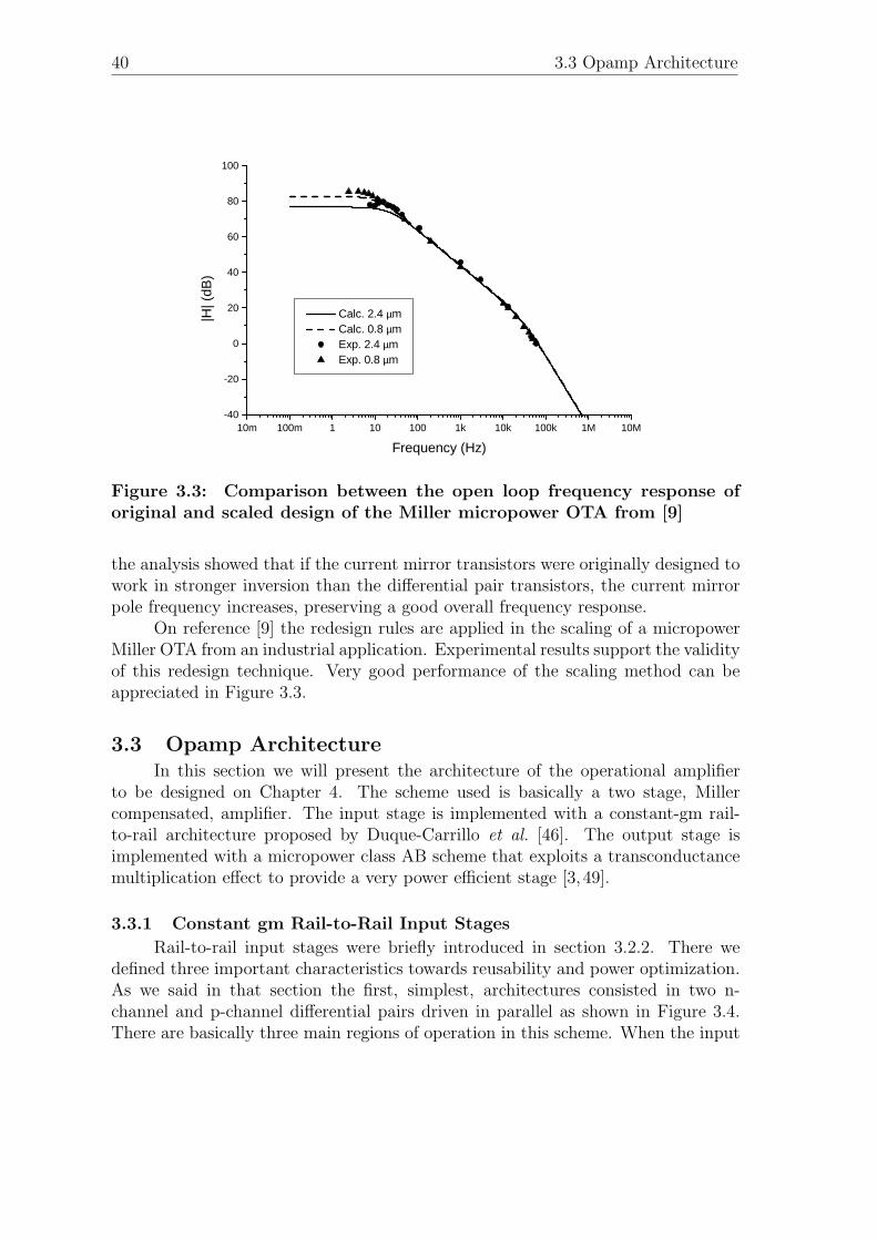
40 3.3 Opamp Architecture
10m 100m 1 10 100 1k 10k 100k 1M 10M-40
-20
0
20
40
60
80
100
Calc. 2.4 µm Calc. 0.8 µm Exp. 2.4 µm Exp. 0.8 µm
|H| (
dB)
Frequency (Hz)
Figure 3.3: Comparison between the open loop frequency response oforiginal and scaled design of the Miller micropower OTA from [9]
the analysis showed that if the current mirror transistors were originally designed towork in stronger inversion than the differential pair transistors, the current mirrorpole frequency increases, preserving a good overall frequency response.
On reference [9] the redesign rules are applied in the scaling of a micropowerMiller OTA from an industrial application. Experimental results support the validityof this redesign technique. Very good performance of the scaling method can beappreciated in Figure 3.3.
3.3 Opamp ArchitectureIn this section we will present the architecture of the operational amplifier
to be designed on Chapter 4. The scheme used is basically a two stage, Millercompensated, amplifier. The input stage is implemented with a constant-gm rail-to-rail architecture proposed by Duque-Carrillo et al. [46]. The output stage isimplemented with a micropower class AB scheme that exploits a transconductancemultiplication effect to provide a very power efficient stage [3, 49].
3.3.1 Constant gm Rail-to-Rail Input Stages
Rail-to-rail input stages were briefly introduced in section 3.2.2. There wedefined three important characteristics towards reusability and power optimization.As we said in that section the first, simplest, architectures consisted in two n-channel and p-channel differential pairs driven in parallel as shown in Figure 3.4.There are basically three main regions of operation in this scheme. When the input

3. Low-Power OpAmp Cells: Reuse, Architecture and Synthesis 41
VDD
VSS
Vin1 Vin2
M1a
M2aM2b
M1b
Ip
In
Figure 3.4: Basic rail-to-rail differential pair architecture.
common mode voltage (VCM) is close to the negative rail (VSS) only the p-channeldifferential pair is on, since the current sink in the n-channel differential pair (In)is out of the constant current saturation region. As we approach mid rail, the n-channel differential pair current sink turns into the saturation region and we haveboth differential pairs working. Finally, when VCM approaches the positive rail(VDD), p-channel current source (Ip) comes out of the saturation region and onlythe n-channel differential pairs remains on. This behavior reflects on non-uniformsmall signal parameters. Particulary the total transconductance (gmT ) might varymore than 100% along the ICMR as can be seen on Figure 3.5.
Non-optimum Frequency Compensation and Power Consumption
We will see how this prevents us from achieving an optimum frequency compen-sation, and therefore, from having an optimum power consumption. Let’s take theMiller amplifier from section 2.4.4 for example. The input stage transconductance ofthis amplifier is gm1 = 1.56µV/A. If we suppose that this amplifier was implemen-ted with the input stage from Figure 3.4 and that gmn = gmp, two possibilities arise:either we implement gm1 with the total transconductance (gm1 = gmT ) or with thetransconductance of each pair (gm1 = gmn = gmp). In either case we end up withnon-optimum solutions. If we design our input stage to have gm1 = gmn = gmp,when VCM is in mid rail the frequency of the gain-bandwidth product (ωT ) doubles(equation (2.27)) and, since the non-dominant pole is independent from gm1 (equa-tion (2.25)), the phase margin is greatly reduced to only 36.4o (both NDP and Zratios are halved)5.
Since this is unacceptable, we should design our input stage to have gmT =gm1. Then, when VCM approaches either rail the gain-bandwidth product is halved.
5This is a first order approximation. The actual ωT will be less than double and thus, the phasemargin might be a bit higher.

42 3.3 Opamp Architecture
0,0 0,5 1,0 1,5 2,0 2,5 3,00,0
1,0µ
2,0µ
3,0µ
4,0µ
5,0µ
gmT
gmn
gmp
gm
(A
/V)
VCM
(V)
Figure 3.5: Transconductance as a function of the input common modevoltage, using architecture from Figure 3.4.
The phase margin, in this case, remains more than adequate. The problem is thatwe are still powering the second stage to keep the non-dominant pole frequency(ωNDP ) far from the mid-rail ωT . Therefore when operating close to the rails, theamplifier is consuming up to two times as much as necessary. This is so, becauseas we saw in section 2.4.4, consumption in a Miller amplifier is dominated by thesecond stage bias current.
Then it is not possible to have optimum frequency compensation and powerconsumption if we do not achieve constant transconductance over the entire inputcommon mode range.
It is interesting to estimate, then, how much current we can invest in having aconstant transconductance. Basically, according to what we have just seen, we couldhalve second stage bias current, when the gain-bandwidth product is halved. But itis more easy to see the problem from the other side. That is, that we could investas much as an additional second stage bias current, needed to preserve frequencycompensation in mid-rail, in keeping the input stage transconductance constant.
Since, the second stage bias current can be expressed in terms of the first stagebias current as
ID2 =gm2
gm1
(gm/ID)1
(gm/ID)2
ID1 (3.10)
in the case of the Miller amplifier designed in section 2.4.4, we could spend up to10.1 times the first stage bias current. Next, when we present the rail-to-rail inputstage used in this work, we will see how many bias current copies does the constanttransconductance auxiliary circuit need, in order to evaluate on the total design if

3. Low-Power OpAmp Cells: Reuse, Architecture and Synthesis 43
+
-
TP,ref
+
-TP
+
-
+
IBP(VCM)
IB
IBN
V
+
-
V+ -
V
+
-
iREFiN
iP
TN
Figure 3.6: Schematic view of the constant gm operation principle.
it was worth it.It is also important to notice, that the time domain response is also closely
related to the frequency response, and thus, its performance will also suffer greatlyfrom the non uniform characteristic of the transconductance. It might even makesense, then, to spend even a little more than the ratio given in equation (3.10), toavoid all the negative effects from having a non-constant input stage transconduc-tance.
Universal and Robust Rail-to-Rail Architecture with Constant-gm
From all the reasons exposed, we selected a rail-to-rail architecture that com-plies with the three characteristics listed in section 3.2.2. Duque-Carrillo et al. [46]proposed a solution that meets the three of them in a very efficient way.
The key to obtain a constant gm input stage lays in obtaining the correct tailcurrent for each differential pair. Duque-Carrillo et al. technique is based on usinga negative feedback loop to impose that:
gmREF = gmP + gmN (3.11)
where gmREF is independent of the input common mode and gmP and gmN are thetransconductances of the input differential pairs.
The negative feedback loop principle is illustrated in Figure 3.6. Here thedifferential pairs TP,ref and TP are identical to the p-channel input stage differentialpair, while TN is identical to the n-channel one. All of them are unbalanced bya DC voltage V, small enough to ensure operation in the linear region. The TP
differential pair is biased by a replica of the p-channel input stage differential pairtail current (IBP ) so it depends on the input common mode, but TP,ref is biasedby a replica of the nominal p-channel tail current (IB) and therefore it’s gm isindependent of the input common mode level. With the polarities shown in Figure

44 3.3 Opamp Architecture
"!#$ % !
& '()( $ #*,+$ - ' $ %
..
Figure 3.7: Implementation of the constant gm technique proposed in[46].
3.6 the differential output currents are added and the voltage of the summing nodecontrols the TN tail current (IBN) as indicated by the dashed line. Doing so, thesum iREF + iP + iN always equals zero and using the small signal model for thedifferential pairs (i = gm× vi) we can easily obtain equation (3.11).
Using a replica of IBN to bias the actual n-channel differential pair of the inputstage we will always have a common mode independent net transconductance in theinput stage equal to gmREF . Since the TP,ref transconductance is independent of anymatching conditions between n- and p-channel input transistors and their operatingregions, the proposed architecture is both robust and universal.
Figure 3.7 shows the circuit implementation of the constant gm technique.The three differential pairs TP,ref , TP and TN are shown. A folded cascode imple-ments the summing circuit. This avoids deviations caused by the mismatch of thecurrent mirrors that would be otherwise required to steer the currents to a summingnode. Also, on the left of the circuit, there is a monitor circuit formed by a fourthdifferential pair whose transistors are identical to the p-channel input ones and withits drain and sources short-circuited. The gates are connected to the amplifier inputsignals, thus, sensing the input common mode and therefore always supplying TP
with the same common mode dependent tail current that biases the p-channel inputdifferential pair.
Figure 3.8 shows the total simulated transconductance of this circuit. In thefigure we can appreciate that differential pair TN doesn’t activate until it is neededand it’s transconductance accurately compensates for the loss of transconductanceon pair TP . On the figure, transconductance from pair TP,ref (gmREF ) is also shown.We can notice a small difference between gmT and gmREF , but it is always below1.6%. Finally, the variations on gmT are less than 0.9% in the whole input commonmode range.
It can be seen then, that since only two of the three differential pairs are alwaysfully active at any moment, this constant gm circuit draws 10ID1 from the supply.This is about the limit we saw for the case of the Miller amplifier from section 2.4.4.But, we will see later, when we study the limit in the case of the complete amplifier,that in that case this is well below the limit for the consumption of the constant gm
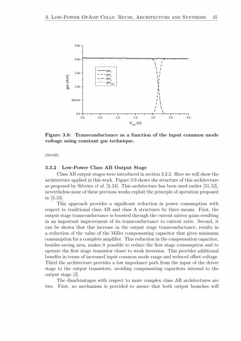
3. Low-Power OpAmp Cells: Reuse, Architecture and Synthesis 45
0,0 0,5 1,0 1,5 2,0 2,5 3,00,0
500,0n
1,0µ
1,5µ
2,0µ
2,5µ
gmT
gmn
gmp
gmREF
gm
(A
/V)
VCM
(V)
Figure 3.8: Transconductance as a function of the input common modevoltage using constant gm technique.
circuit.
3.3.2 Low-Power Class AB Output Stage
Class AB output stages were introduced in section 3.2.2. Here we will show thearchitecture applied in this work. Figure 3.9 shows the structure of this architectureas proposed by Silveira et al. [3,24]. This architecture has been used earlier [51,52],nevertheless none of these previous works exploit the principle of operation proposedin [3, 24].
This approach provides a significant reduction in power consumption withrespect to traditional class AB and class A structures by three means. First, theoutput stage transconductance is boosted through the current mirror gains resultingin an important improvement of its transconductance to current ratio. Second, itcan be shown that this increase in the output stage transconductance, results ina reduction of the value of the Miller compensating capacitor that gives minimumconsumption for a complete amplifier. This reduction in the compensation capacitor,besides saving area, makes it possible to reduce the first stage consumption and tooperate the first stage transistor closer to weak inversion. This provides additionalbenefits in terms of increased input common mode range and reduced offset voltage.Third the architecture provides a low impedance path from the input of the driverstage to the output transistors, avoiding compensating capacitors internal to theoutput stage [3].
The disadvantages with respect to more complex class AB architectures aretwo. First, no mechanism is provided to assure that both output branches will

46 3.3 Opamp Architecture
1
1
1
h
m
k
IQ
V D D
Vin
Mf
M b
M e
M a
Mc
M d
IAB
C L
Figure 3.9: Class AB output stage proposed by [3].
always remain in conduction. This, as mentioned in section 3.2.2, leads to increasedringing in the time response for high amplitude steps and increased distortion, dueto the increased delay associated to the branch that cuts off. Second, the ratio ofthe maximum output current to the quiescent current is fixed by the current mirrorgains. As we will see below, the maximum allowable value of these gains is limiteddue to its effect on stability. Thus, the ratio of maximum output current to quiescentcurrent is also limited. In spite of this, a significant reduction in consumption withrespect to a class A case is achieved [3].
Distortion is an additional possible concern. The transconductance multipli-cation effect is based on an asymmetric behavior of the p and n sections of theoutput stage, hence leading to a non linear behavior of the output stage. However,as shown in [3] the high gain achieved by this stage allows to reach very reasonabledistortion figures.
We will now sum up the main characteristics of this architecture as presentedin [3]. The quiescent current is fixed with respect to the IAB current source fromFigure 3.9. In quiescent conditions the output current is zero and the output branchquiescent current IQ must be such that the sum of the scaled versions of IQ at Meand Mf is equal to IAB. This conditions yields
IQ =km
1 + kmh
IAB (3.12)
where h, k and m are the gain factors of the current mirrors shown in Figure 3.9.The total quiescent transconductance of this stage under class AB operation,
defined as the ratio between the total signal output current io and the input signalvoltage vi is given by:
gmAB = gma
(1 +
km
h
)D(s) (3.13)

3. Low-Power OpAmp Cells: Reuse, Architecture and Synthesis 47
where gma is the transconductance of the output transistor Ma and D(s) representsthe contribution to the frequency response of the current mirrors. The factor 1+ km
h
that multiplies the transconductance is noted gmmult, and although D(s) mightintroduce high frequency doublets, the circuit can be properly stabilized even forfactors as high as 25.
It is also interesting to consider the effect on the transconductance to consumedratio (gm/ID) of the stage.
(gm/ID) = (gm/ID)a
1 + kmm
1 + 1k
+ 1km
+ 1h
D(s) (3.14)
In this case, multiplication factors as high as 12 can be achieved. This is like havingan equivalent transistor 12 times more efficient than the original one.
The factor D(s) is given by equation (3.15) [3], where ωe (ωc) is the angularfrequency of the pole of the current mirror Mb−Mc (Md−Me).
D(s) =1 +
(1ωe
+ 1ωc
)s
gmmult+ 1
ωeωc
s2
gmmult(1 + s
ωe
) (1 + s
ωc
) (3.15)
Both angular frequencies are given by equations (3.16) and (3.17).
ωe =gme
Ce
(3.16)
ωc =gmc
Cc
(3.17)
where gme (gmc) is the transconductance of the Me (Mc) transistor and Ce (Cc)is the total capacitance at the Me (Mc) gate node. The doublet introduces animportant phase shift near the ωe and ωc frequencies. This effect determines themaximum acceptable values for the gmmult factor.
Lets summarize the factors that determine the achievable total consumptionreduction. Consider we apply this output stage as the second stage of a Milleramplifier, in which the Miller capacitance is connected between the input and outputnodes of the circuit in Figure 3.9. Since the non-dominant pole of this amplifier isproportional to the second stage transconductance (equation (2.25)), the secondstage current will decrease according to the increase in the (gm/ID) ratio, whencompared to the class A output stage used in the amplifier from section 2.4.1. Theimprovement in the (gm/ID) ratio is not completely translated into a reduction ofthe current. The reason is that the non-dominant pole must be increased, withrespect to the class A case, to have the same phase margin while allowing the phaseshift introduced by the doublets. Taking these factors into account, reductions ofquiescent current, with respect to the class A case, by a factor of 3 to 4 are reportedin [3] to be achievable. In this work, we obtained a factor of 4, in spite that our non-dominant pole has to be increased even more due to the presence of non dominant

48 3.4 Advanced Design Methodologies
Figure 3.10: Amplifier circuit implementation, omitting constant-gm cir-cuit.
poles in the input stage folded cascode (Figure 3.10).The maximum output source current is given by kmIAB, while the maximum
output current the stage is capable to sink is limited by the size of Ma and themaximum voltage at the input of the stage.
This output stage has already been successfully used in a very low powerconsumption ([email protected] ) pacemaker sensing channel application [23].
3.3.3 Opamp Complete Architecture
These two stages are used in a Miller amplifier architecture. The rail-to-railinput stage is used instead of the single differential pair input stage used in the Milleramplifier from section 2.4.1. In order to provide a single high impedance node wherethe output stage and the compensating network is connected, we sum the outputcurrents of the complementary input differential pairs using the same folded cascodesumming circuit used in the constant-gm technique (Figure 3.7). Besides, this stagewill provide additional gain to the amplifier.
The compensating capacitor, is substituted with a R-C compensating network.The R-C network eliminates the right half plane zero of the Miller amplifier, makingit possible to reduce the overall consumption by further decreasing the requirementson the second stage transconductance. The RC compensation introduces an addi-tional non-dominant pole, but it can be shown to lie at much higher frequenciesthan the first non-dominant pole, associated to the load capacitance. The completeamplifier schematic, omitting the constant-gm circuit shown in Figure 3.7, is shownin Figure 3.10.
3.4 Advanced Design MethodologiesWhen developing design methodologies towards a given objective several fac-
tors and aspects of the amplifier must be taken into account. All this data can behierarchically represented in three levels (high, medium and low), where data in each

3. Low-Power OpAmp Cells: Reuse, Architecture and Synthesis 49
lower level combine to determine the next level performance. In the case of powerconsumption, “high level” data can be represented by the static and dynamic pre-cision and the total noise of the amplifier. These characteristics are determined bythe “medium level” data that is represented, in turn, by transition frequency, phasemargin, slew rate, thermal and flicker noise, DC gain and so on. All of which aredetermined by the “low level” data: transistor’s sizes, currents and capacitances [3].
In the conventional design practice, the step that goes from the high level per-formance data to the medium level performance data that guides amplifier design,has been rather fuzzy. Silveira [3,22] presents a new approach to transit systemati-cally from the high level total settling time specification to a low level design thatcomplies with these specifications with optimum power consumption. This approachis based on the (gm/ID) methodology [1] that allows a systematic exploration of thedesign space to implement the step that goes from the medium level op amp spe-cifications to the low level design data, as in the case of Algorithm 2.2 that waspresented in Chapter 2.
This new approach, was implemented in a power optimization algorithm fora given total settling time. Though it can be easily applied in other amplifiersarchitectures, it was developed to be applied in a Miller RC compensated amplifier.This algorithm will be presented in section 3.4.1 as was presented in [3, 22]. Then,in Chapter 4, we will further develop this algorithm in a more general, hierarchicaldesign methodology that will allows us to automatically synthesize the amplifierpresented in section 3.3 with optimum power consumption for a given total settlingtime.
3.4.1 Power Optimization for a Given Total Settling Time
The total settling time is defined as the time the response to an input stepwill take to settle to a given relative error (e.g. 1%) of its final value. The settlingbehavior is an essential specification in most op amp applications, as it is a directmeasure of the ability of the amplifier to respond to large input signals.
Two distinct periods determine the settling time: the slewing period and thelinear settling period. During the first period, the variation rate of the outputis limited to a maximum value (slew rate). This originates from the charging of acapacitive node with a limited, constant current. This node can be either an internalnode or the output node. We will refer to the first case as internal slew rate andto the second one as external slew rate. In the linear settling period, the amplifierbehaves according to its small signal frequency response, and thus is related to theamplifier transition frequency and phase margin.
A given total settling time can be achieved with different distributions betweenthe linear settling and the slewing part. Which is the best alternative to this dis-tribution is still a subject of study and Silveira [3] shows that the selected partitionstrongly influences power consumption
To find the optimum distribution, Silveira [3,22] developed a settling behaviormodel to be applied in a power optimization algorithm for a given total settling
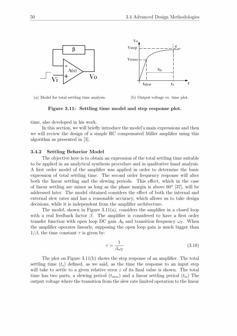
50 3.4 Advanced Design Methodologies
-+ VoVi
A(s)
b
(a) Model for total settling time analysis.
tls
tstslew
Vtrans
Vstep
t
Voe
(b) Output voltage vs. time plot.
Figure 3.11: Settling time model and step response plot.
time, also developed in his work.In this section, we will briefly introduce the model’s main expressions and then
we will review the design of a simple RC compensated Miller amplifier using thisalgorithm as presented in [3].
3.4.2 Settling Behavior Model
The objective here is to obtain an expression of the total settling time suitableto be applied in an analytical synthesis procedure and in qualitative hand analysis.A first order model of the amplifier was applied in order to determine the basicexpression of total settling time. The second order frequency response will alterboth the linear settling and the slewing periods. This effect, which in the caseof linear settling are minor as long as the phase margin is above 60o [37], will beaddressed later. The model obtained considers the effect of both the internal andexternal slew rates and has a reasonable accuracy, which allows us to take designdecisions, while it is independent from the amplifier architecture.
The model, shown in Figure 3.11(a), considers the amplifier in a closed loopwith a real feedback factor β. The amplifier is considered to have a first ordertransfer function with open loop DC gain A0 and transition frequency ωT . Whenthe amplifier operates linearly, supposing the open loop gain is much bigger than1/β, the time constant τ is given by:
τ =1
βωT
(3.18)
The plot on Figure 3.11(b) shows the step response of an amplifier. The totalsettling time (ts) defined, as we said, as the time the response to an input stepwill take to settle to a given relative error ε of its final value is shown. The totaltime has two parts, a slewing period (tslew) and a linear settling period (tls) Theoutput voltage where the transition from the slew rate limited operation to the linear

3. Low-Power OpAmp Cells: Reuse, Architecture and Synthesis 51
operation occurs is denoted Vtrans.The expression of the total settling time, taking into account the slewing and
the linear part, is given by [3, 22]:
ts = tslew + tls = τ
[ln
(1
ε
)− 1 + ln (x) +
1
x
](3.19)
where
x =τSR
Vstep
=Vstep − Vtrans
Vstep
(3.20)
Therefore, x is a dimensionless magnitude which has values between 0 and 1. Itsphysical meaning is that it corresponds to the fraction of the total step where wehave linear settling.
The fact that the amplifier has actually a second order response, can be takeninto account by introducing two changes to equation (3.19). First, calculating τ withthe actual transition frequency and not the first order one, which for a given phasemargin is achieved including in the expression of τ in equation (3.18) a correctioncoefficient kcorrωT
that multiplies ωT . Second, multiplying the ln(1/ε) term by acorrection coefficient (kcorrsetl) that takes into account the different evolution of thesecond order time response, and hence change the number of time constants requiredto settle for a given phase margin.
This model, including the above mentioned correction factors, was appliedin [3, 22] to evaluate the total settling time at 5% of an experimental class AB9MHz OTA.
3.4.3 Power Optimization of a Miller OTA
The power optimization methodology was developed for a RC compensatedMiller OTA. As we said in section 3.3.3, the RC compensation network makes itpossible to reduce the power consumption of a Miller amplifier.
Phase margin, in the RC compensated Miller, is a function of the first ordertransition frequency (2.27) and the non-dominant pole frequency (2.25).
PM = f (ωT , ωNDP ) (3.21)
Both expressions for these frequencies, seen on section 2.4.1, still stand when usingthe RC compensation.
ωT =gm1
Cm
(2.27)
ωNDP =gm2Cm
C1C2 + Cm(C1 + C2)(2.25)

52 3.4 Advanced Design Methodologies
while a third pole appears
ωRC =1
RmCm
where Rm is the resistance in the RC compensating network. It can be proved [37]that this last pole lies at much higher frequencies, and thus, can be neglected inequation (3.21).
The slew rate is defined as the minimum between the internal slew rate andthe external slew rate. Internal slew rate will be noted SR1 and in the case of theMiller amplifier originates from the charging of the compensating capacitance Cm.External slew rate will be noted SR2 and in the case of the class A output stage,originates from the charging of the load capacitance.
SR = min SR1, SR2 (3.22)
with
SR1 =2ID1
Cm
(3.23)
SR2 =ID2
C2
(3.24)
where ID1(2), Cm and C2 were defined in section 2.4.1.An additional equation will be needed for the determination of the compensa-
tion capacitance. Silveira [3,22] presents two approaches. One, is from the fact thatthe compensation capacitance basically determines the thermal noise characteristicof the amplifier [53]. Therefore,we could determine Cm from the noise specification.
A second way to determine Cm is from the effect it has on power consump-tion. If we consider a given gain-bandwidth product, equation (2.27), shows thatan increase in Cm requires an increase in the first stage transconductance and thusan increase in the first stage current. On the other hand, for a given phase margin,and thus for a given non-dominant pole frequency, equation (2.25), it can be seenthat an increase in Cm results in a decrease in the second stage transconductanceand hence in its current. Therefore, it exists a Cm value that results in a minimumtotal current, for a given gain-bandwidth product and phase margin.
So far, in the previous equations, we have five unknowns: the (W/L) ratio andcurrent of the input and output transistors and the compensating capacitor. It canbe seen that this is equivalent to have the (gm/ID) ratio of the input and outputtransistors, the current of the output transistor (ID2), the gain bandwidth product(ωT ) and the compensating capacitance (Cm). The equations are three, equation(3.21) to have a given phase margin, equation (3.19) to have a given total settlingtime and either condition that determines the compensation capacitance. Hence wehave two degrees of freedom that we will assign to the (gm/ID) ratios of the inputdifferential pair ((gm/ID)1) and the output stage active transistor ((gm/ID)2). We

3. Low-Power OpAmp Cells: Reuse, Architecture and Synthesis 53
will be able then to perform a design space exploration, as in Algorithm 2.2, todetermine the optimum combination of (gm/ID)1 and (gm/ID)2 that minimizespower consumption for a given settling time and phase margin.
In Algorithm 3.1 the power optimization algorithm for a given total settlingtime developed in [3] is presented. This algorithm only calculates the dimensions oftransistors M1 . . .M3, the dimensions of the current sources transistors (M4 andM5) can be later sized using similar criteria to the criteria used on Algorithm 2.2.
This algorithm has the interesting feature that it can be very easily appliedto other amplifier architectures. This is based, first, on the fact that the totalsettling time model shown above and presented in [3, 22], is fairly independent ofthe particular amplifier architecture. On top of that, the most general concept ofexploring the design space through the (gm/ID) method to search the minimumconsumption for a given total settling time, can be applied to any amplifier. Whatwe need is to adapt the design procedure described for the Miller RC amplifier insteps 3(a) to 3(e).
This procedure is based on the two expressions that relate the first order tran-sition frequency with the input stage (gm/ID) ratio and the non dominant pole withthe output stage (gm/ID) ratio (equations (2.27) and (2.25)). These same relationsare present in other amplifiers and, thus, can be used to develop the particularprocedure for that particular amplifier.
3.5 ConclusionsThe main ideas in analog design reuse and advanced design methodologies have
been presented. We have shown that circuit performance tuning is possible and wehave reviewed the desirable characteristics of a reusable opamp architectures. Thenwe showed a particular implementation of these characteristics in a two stage RCMiller compensated amplifier with rail-to-rail input stage and class AB output stage.
Also, technology migration was briefly explained as a valid alternative in ana-log design reuse, including experimental results.
Then, a power optimization algorithm for a given total settling time, presentedby Silveira [3,22], was reviewed as an example of advanced design methodology. Thisalgorithm effectively transits systematically from high level total settling time spe-cification to a low level design that complies with these specifications with optimumpower consumption.
This algorithm, can be very easily applied to other amplifier architectures. Inthe case of a Miller amplifier with more complex input and output stages’ architec-tures, we only need to rewrite some of the equations used here.
This is what we intend to do in Chapter 4, when we will develop a hierarchicalalgorithm to synthesize the Miller amplifier presented in section 3.3.

54 3.5 Conclusions
Algorithm 3.1 Power Optimization for a Given Total Settling Time
1. The lengths of the active transistors are taken of minimum value. Thisvalue can be later increased if the resulting DC gain is not enough or the1/f noise is too big.
2. Mirror transistors are designed to minimize systematic offset as in Algo-rithm 2.1.
3. The design space is swept. For each point in the design space we swept Cm.For each value the amplifier is designed to comply with the specified totalsettling time and phase margin. This is done with the following iterativeprocedure:
(a) Initial values for ωT and ID2 are determined using equations (2.25),(3.19), (3.20) and (3.22)in the simplified case where C1 ¿ Cm ¿ C2
and SR1 < SR2.
(b) ID1 is determined as:
ID1 =ωT Cm
(gm/ID)1
(c) We can now determine the size of transistors M1 . . . M3 since the(gm/ID) ratio and current is known for all of them.
(d) From the calculated transistor sizes, we calculate the parasitic capa-citance C1. Then, we can calculate x, ωT and ID2 using the followingexpressions derived from equations (2.25), (3.19), (3.20) and (3.22).
x =min
2
(gm/ID)1, NDP (C1C2+Cm(C1+C2))
(gm/ID)2 CmC2
βVstep(3.25)
ωT =
(ln
(1ε
)− 1 + ln(x) + 1x
)
βts(3.26)
ID2 = ωTNDP (C1C2 + Cm(C1 + C2))
(gm/ID)2 Cm(3.27)
(e) If the relative differences with the initial values of ωT and ID2 is lessthan a given error the procedure is finished, else we iterate at step3(b) with the newly calculated values.

Chapter 4Hierarchical Automated Synthesis
4.1 IntroductionThis Chapter intends to apply to ideas seen on the last chapter to automa-
tically synthesize a reusable operational amplifier cell. Since we are using a muchmore complex architecture seen on Chapter 3, we need to adapt the algorithms seenso far to take into account the added complexity.
First, section 4.2 presents an expression developed in this work to directlyobtain the value of the Miller compensating capacitance that minimize power con-sumption. This expression saves large amounts of processing time, since it is nolonger necessary to sweep the value of Cm and synthesize the whole amplifier foreach value to find the optimum design. However, this expression must be used withcare as will be seen below.
Section 4.3 presents the hierarchical automated synthesis algorithm that wasdeveloped in this work. The algorithm independently synthesize each stage and thencombines its results in a high level algorithm based on the algorithm seen on section3.4. The results of this algorithm are presented in section 4.4, including simulationresults, and examples of the performance tuning capabilities of the opamp cell.
Conclusions are presented in section 4.6 and experimental results are presentedin Chapter 5.
4.2 Miller Compensation Capacitance for Minimum PowerConsumption
Algorithm 3.1 uses a very robust but very time consuming method to obtainthe compensation capacitance (Cm) that provides minimum power consumption ina given design space location. We will try here to obtain an expression for thiscapacitance, in order to use it in the proposed algorithm.
The total quiescent current consumption in the amplifier can be expressed as
IDD = α1ID1 + α2ID2 (4.1)
where α1 and α2 is the number of times each of the stage’s bias currents is drawnfrom the source in quiescent conditions. In the case of the simple Miller OTApresented in section 2.4.1, α1 = 2 and α2 = 1. In the case of the amplifier presentedin section 3.3, α1 = 16 and α2 = 1 + 1
h+ 1
k+ 1
km.
Bias currents can be written as functions of the compensation capacitance
55

56 4.3 Synthesis Algorithm
using equations (2.27) and (3.27)
ID1 =gm1
(gm/ID)1
=ωT Cm
(gm/ID)1
(4.2)
ID2 = ωTNDP (C1C2 + Cm(C1 + C2))
(gm/ID)2 Cm
(4.3)
In order to obtain the compensation capacitance (Cm) that minimizes the totalconsumption (IDD), we must null the derivative of equation (4.1). Several factors inthe above expression are also functions of Cm (ωT , C1, C2, etc.) and should be alsotaken into account when calculating the derivative. However, these dependenciesare very hard to obtain and very dependent on the stage architecture. Since we willbe using this expression in an iterative algorithm that will asymptotically tend tothe solution, we will consider all these factors as constant in a small interval aroundthe actual value of Cm.
dIDD
dCm
= α1ωT
(gm/ID)1
− α2ωT NDP
(gm/ID)2
C1C2
C2m
= 0 (4.4)
d2IDD
dC2m
= 2α2ωT NDP
(gm/ID)2
C1C2
C3m
> 0 (Cm > 0) (4.5)
Equation (4.5) proves that the zero in equation (4.4) corresponds to a minimumand confirms that there is a value for Cm that minimizes consumption, as stated bySilveira in [3] and section 3.4.1.
Then using equation (4.4), we obtain the expression for minimum consumptionCm:
Cm =
√α2NDP (gm/ID)1 C1C2
α1(gm/ID)2
(4.6)
This expression becomes a very useful tool towards saving important processingtime in the synthesis of Miller amplifiers using Algorithm 3.1. The validity of thisexpression can be confirmed referring to the design obtained by Silveira [3] usingAlgorithm 3.1. He obtained optimum consumption with Cm = 2pF , while equation(4.6) yields Cm = 1.87pF . The difference not only is less than the step used bySilveira to sweep Cm, but also is deep within the process variations.
However, equation (4.6) must be used with care, since it makes an importantapproximation when considers C1 and C2 as constants and, thus, it should be usedonly in iterative processes as Algorithm 3.1.
4.3 Synthesis AlgorithmThe amplifier presented in section 3.3 has a much more complex architecture
than the simple Miller amplifier used in the synthesis algorithms presented in sec-tions 2.4 and 3.4.1. Then, to develop a synthesis algorithm for our amplifier we willuse a hierarchial approach. That is, we will consider our amplifier as a two-stage,

4. Hierarchical Automated Synthesis 57
Figure 4.1: High Level Schematic of the Amplifier
RC Miller compensated amplifier, and thus, use the same algorithm presented insection 3.4.1, but making modifications to take into account that each stage needsto be synthesized to obtain its high level characteristics. We will show that thishierarchical approach is feasible in spite of the fact that variables in analog designare strongly coupled.
This can be seen in Figure 4.1, where each stage is characterized by 4 para-meters: transconductance, gm, output conductance, go, input capacitance, Ci andoutput capacitance, Co. Then, a high level synthesis can be used independently ofthe implementation of each stage, provided that the internal poles and zeros of eachstage are taken into account. The two stage amplifier model is completed with
C1 = Co1 + Ci2 (4.7)
C2 = Co2 + CL (4.8)
Rm =1
gm2
(4.9)
Thus, we have 5 unknowns at this point:
gm1
gm2
ID1
ID2
Cm
⇒
(gm/ID)1
(gm/ID)2
ID1
ID2
Cm
(4.10)
which are more conveniently written in the form of the second brace.Now we can sweep the design space, defined as always by the (gm/ID) ratio
of each stage, to obtain in each point, minimum consumption designs that complywith the total settling time and phase margin specifications.
Figure 4.2 shows the synthesis scheme for the amplifier. For each point of the

58 4.3 Synthesis Algorithm
!"
"""
"
! !#!
! !
$%#&
$%#&
'()
*"+,#*"+,
""
-.$#!-%/0
Figure 4.2: Complete Amplifier Synthesis Algorithm Scheme. tsett is totalsettling time and IDD is total current consumption.
design space, we perform a high level synthesis of the amplifier to obtain minimumconsumption for the specifications given. In each step of the synthesis, input andoutput stage are re-synthesized and we update the high level characteristics of themto be used in the next step of the high level synthesis. When it converges to a finalvalue, we move on to the next point in the design space, until we have explored theconsumption space of the amplifier, as in sections 2.4.4 and 2.4.5 (see Figure 2.5 andFigure 2.12). There, we can choose the point of minimum consumption from whichwe can obtain our final design. The final step is a performance evaluation of thisdesign, to assure that we have all other aspects of the amplifier at acceptable values.In case we find something out of specifications, we should change some preselectedparameter (e.g. transistor’s lengths) and rerun the synthesis.
The high level synthesis will be a modified version of the Algorithm 3.1 inclu-ding the direct estimation of Cm by equation (4.6). Next we will see how we willmodify the algorithm and how we will implement the synthesis algorithms for eachstage.
4.3.1 High Level Synthesis
When considering the (gm/ID) ratio of each stage, we have two choices. Eitherconsider the ratio between the effective transconductance of the stage over the to-tal current consumption of the stage; or consider the (gm/ID) ratio of the activetransistors of each stage.
The first choice, is clearly more in the spirit of a hierarchical synthesis algo-

4. Hierarchical Automated Synthesis 59
rithm and would allow us to use the same equations used in Algorithm 3.1. However,these (gm/ID) ratios would depend on the stage synthesis, and thus, could not pos-sibly be used to define the design space as we have used the (gm/ID) ratios so far.Which ultimately means that we could not use Algorithm 3.1 at all.
On the other hand, the second choice allows us to define the design spaceindependently of the outcome of each step of the algorithm, since the (gm/ID) ratiocharacteristic of a transistor is defined by its technology. Thus, although having torewrite some of the equations, this option allow us to use Algorithm 3.1 as the highlevel synthesis algorithm of our amplifier.
In conclusion, for the input stage we will use the (gm/ID) ratio of the TP,ref
differential pair transistors, from now on noted (gm/ID)1. And for the output stagewe will use the (gm/ID) ratio of transistor Ma, from now on noted (gm/ID)2 (seeFigures 3.7 and 3.9). Regarding (gm/ID)2, note that (gm/ID)2 = gma/IDa. Then,to have an uniform criterium, we will refer to gma and IDa as gm2 and ID2 respec-tively.
Let’s see now, how does the equations from Algorithm 3.1 ought to be modified.The gain-bandwidth product remains unchanged, but the expression for the non-dominant pole frequency
ωNDP =gm2Cm
C1C2 + Cm(C1 + C2)(2.25)
has to take into account that, according to equation (3.13), the effective transcon-ductance from the output stage is augmented by a gmmult factor, and thus, the newexpression for the non-dominant pole frequency is
ωNDP0 =gm2gmmult Cm
C1C2 + Cm(C1 + C2)(4.11)
where the subscript 0 is because we have considered that the effect of the pole-zero doublets of the output stage (equation (3.15)) is negligible (e.g. D(s) = 1).Of course, this has to be taken into account when synthesizing the output stage.Then, the NDP factor (NDP = ωNDP0
ωT) will not be given a priori, but will be
obtained from the output stage synthesis, where we can evaluate where should thenon-dominant pole lie to have a given phase margin in spite of the pole-zero doubletsof the output stage.
It is worth stopping a moment here to take notice on the effect that the gmmult
factor has on the size of Cm and ultimately on the current consumption6 and theavailable current budget for the constant gm circuit. It can be easily seen thatequation (4.11) yields smaller Cm values for the same ωNDP when gmmult > 1.This translates in smaller currents in the input stage transistors to obtain the samegain-bandwidth product. Thus, we end up with less total consumption, although,
6This fact was first mentioned when introducing the output stage in section 3.3.2 and here wecan show the cause.
60 4.3 Synthesis Algorithm
since the latter is dominated by the second stage current consumption, this effectdoesn’t lead to big savings. However, what is interesting here, is that we have anumber of benefits in this negligible current consumption save. As we mentioned insection 3.3.2, we can work our input stage in weaker inversion with all the benefitsthat yields in terms of increased input common mode range, increased gain andreduced input offset voltage.
What we did not mention earlier is that the ratio between output and inputstage bias currents has become almost gmmult bigger. Thus, recalling what we sawin section 3.3.1, now we have enlarged the current budget available for the constantgm circuit by the same gmmult factor. Therefore it makes even more sense now, toinvest the 10 copies of the input stage bias current needed to keep the input stagetransconductance constant, since its effect on the total current consumption of theamplifier has become truly negligible7.
Resuming with the rewriting of the expressions from Algorithm 3.1, we willanalyze how internal and external slew rate expressions are modified.
The internal slew rate (SR1) will be given by the maximum output current ofthe first stage, that is the maximum output current of the folded cascode summingcircuit (see Figure 3.10). Since we are biasing them with 2ID1, it is well known thatthe maximum output current, and thus the slew rate, is the same that the one fora single differential pair. Therefore the expression for the internal slew rate (givenin equation (3.23)) remains unchanged.
The external slew rate (SR2) will be given by the maximum output current ofthe second stage. As we saw in section 3.3.2 the output current is non-symmetrical.The maximum current the stage can source is
IoMAX(+) = gmmult ID2 (4.12)
while the maximum current the stage can sink is given by the size of Ma and themaximum voltage swing at the input of the stage.
Since this last value can’t be known before the transistor has been synthesized,we will use equation (4.12) and then assure that the maximum current the stagecan sink is above that value.
Finally, then, we can rewrite equation (3.20) as
x =min
2
(gm/ID)1, gmmult ID2
ωT C2
βVstep
(4.13)
where the expression for ID2 has to be rewritten from equation (3.27) as
ID2 = ωTNDP (C1C2 + Cm(C1 + C2))
(gm/ID)2 gmmult Cm
(4.14)
taking into consideration the augmented effective transconductance of the output
7Usually gmmult factor can reach values between 15 and 25. In our case, gmmult is equal to 22

4. Hierarchical Automated Synthesis 61
stage.In Algorithm 3.1 the value for Cm is swept. In this new algorithm we will use
the expression derived in section 4.2. However, during this work we saw that if weuse the value obtained from equation (4.14) using equation (4.6) to calculate Cm,the algorithm had severe convergence problems. This can be explained reviewingthe assumptions made to obtain equation (4.6). That expression is valid only in asmall interval around the previous step value for Cm, since it considered constantseveral parameters that in fact, are not constant in the whole range of valid Cm
values.Thus, we choose to smooth the change to the next value of ID2 to comply
with the assumptions made to obtain equation (4.6). To do this, we calculate thedifference between the actual value and the new estimation,
∆ID2 = ωTNDP (C1C2 + Cm(C1 + C2))
(gm/ID)2 gmmult Cm
− ID2 (4.15)
and then calculate the new value as
ID2new = ID2 + α∆ID2 (4.16)
where we defined α as the “iteration step”, which can be either constant or adaptivewith ∆ID2
8.It is worth making one final remark on the value of Cm. As we have men-
tioned, the effect of the gmmult factors might yield very low values for Cm. Weeven encounter values as low as some tens of fF . This of course is unacceptable,since it would yield high noise figures and would be hardly implementable due tothe uncertainty in the actual value. Then, we chose to establish a bottom limit forCm and check each time that the limit is respected. Therefore, instead of equation(4.6), we will use
Cm = min
CmMIN ,
√α2NDP (gm/ID)1 C1C2
α1gmmult (gm/ID)2
(4.17)
where we chose CmMIN = 0.25pF .In Algorithm 4.1 the high level synthesis algorithm is presented. Here we see
how we did implement the main ideas presented in this section. Steps 4(a) and 4(c)are calls to Algorithm 4.3 and Algorithm 4.2, which implement the output and inputstage synthesis respectively. These algorithms are presented next.
4.3.2 Input Stage Synthesis
The input stage synthesis, although might look complicated because of all theconstant transconductance circuitry, is quite simple. This is so, because once we
8In the last version of the algorithm, we use the hyperbolic tangent function (tanh) to implementan adaptive step that goes from 0.1 to 1.

62 4.3 Synthesis Algorithm
Algorithm 4.1 High Level Synthesis
1. (gm/ID)1 and (gm/ID)2 ratios are given by the design space sweep.
2. Initial values for x, ωT and ID2 are determined using equations (4.13),(3.26) and (4.14) in the simplified case where C1 ¿ Cm ¿ C2 and NDP =2.2.
3. We estimate values for k, h,m, C1 and C2 ' CL. Then we can estimate aninitial value for Cm using equation (4.17).
4. We perform the following iterative process:
(a) Using ID2 we synthesize the output stage. We obtain Ci2, Co2, NDPand k, h, m.
(b) From k, h,m we calculate gmmult and the factor α2 for equation(4.17).
(c) Using Cm we synthesize the input stage. We obtain Co1 and ID1.
(d) From the calculated parasitic input and output capacitances, we cal-culate the C1 and C2.
(e) Using equations (4.15) and (4.16) we calculate ID2.
∆ID2 = ωTNDP (C1C2 + Cm(C1 + C2))
(gm/ID)2 gmmult Cm− ID2
ID2new = ID2 + α∆ID2
(f) Using equations (4.13), (3.26) and (4.17) we calculate x, ωT and Cm
respectively.
x =min
2
(gm/ID)1, gmmult ID2new
ωT C2
βVstep
ωT =
(ln
(1ε
)+ ln(x) + 1
x
)
βts
Cm = min
CmMIN ,
√c2NDP (gm/ID)1 C1C2
c1gmmult (gm/ID)2
(g) If the relative difference between ID2new and ID2 is less than a givenerror the procedure is finished, else we iterate at step 4(a) with thenewly calculated values.
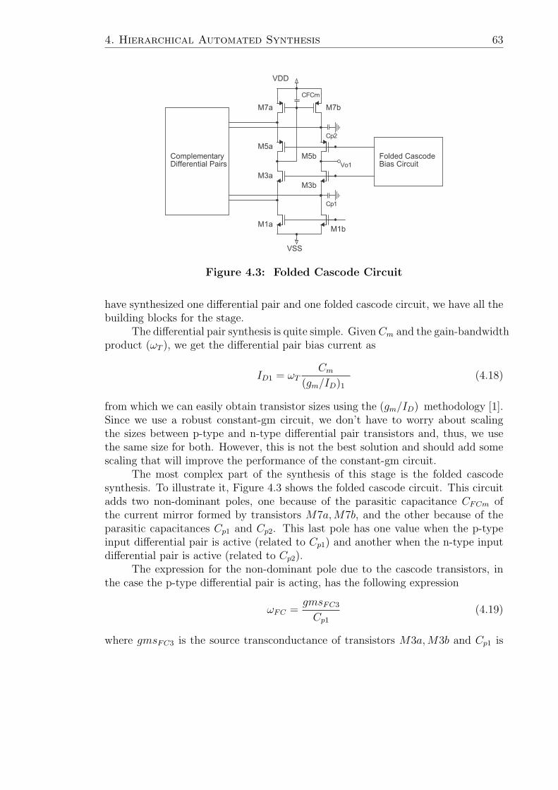
4. Hierarchical Automated Synthesis 63
Figure 4.3: Folded Cascode Circuit
have synthesized one differential pair and one folded cascode circuit, we have all thebuilding blocks for the stage.
The differential pair synthesis is quite simple. Given Cm and the gain-bandwidthproduct (ωT ), we get the differential pair bias current as
ID1 = ωTCm
(gm/ID)1
(4.18)
from which we can easily obtain transistor sizes using the (gm/ID) methodology [1].Since we use a robust constant-gm circuit, we don’t have to worry about scalingthe sizes between p-type and n-type differential pair transistors and, thus, we usethe same size for both. However, this is not the best solution and should add somescaling that will improve the performance of the constant-gm circuit.
The most complex part of the synthesis of this stage is the folded cascodesynthesis. To illustrate it, Figure 4.3 shows the folded cascode circuit. This circuitadds two non-dominant poles, one because of the parasitic capacitance CFCm ofthe current mirror formed by transistors M7a,M7b, and the other because of theparasitic capacitances Cp1 and Cp2. This last pole has one value when the p-typeinput differential pair is active (related to Cp1) and another when the n-type inputdifferential pair is active (related to Cp2).
The expression for the non-dominant pole due to the cascode transistors, inthe case the p-type differential pair is acting, has the following expression
ωFC =gmsFC3
Cp1
(4.19)
where gmsFC3 is the source transconductance of transistors M3a,M3b and Cp1 is

64 4.3 Synthesis Algorithm
given byCp1 = CoDP + CjFC3 + CjFC1 + CGSFC3 (4.20)
where CoDP is the output capacitance of the differential pair, CjFC1(3) is the junctiondrain-bulk capacitance of transistors M1b (M3b) and CGSFC3 is the gate source ca-pacitance of transistors M3b. This means that the parasitic capacitance is partiallydetermined by the differential pair synthesis and transistor M1b, which is a currentsource designed a priori.
However it also depends on the (gm/ID) ratio of transistor M3b, and recallingthat gms = ngm, we can sweep the (gm/ID)FC3 ratio of the cascode transistors toobtain the corresponding frequencies of this non-dominant pole. Since the currentthrough the cascode transistor is 2ID1, we can express the non-dominant pole fre-quency as
ωFC =2ID1n(gm/ID)FC3
Cp1
(4.21)
It can be seen that there is a (gm/ID)FC3 ratio in which the NDPFC = ωFC
ωT
ratio is maximum. Thus, we design our transistors M3a,M3b to obtain maximumNDPFC . To size transistors M5a,M5b we use an analogue procedure. The existenceof this maximum is yet another example of the trade off between the increase in thetransconductance and the increase in the parasitic capacitances when operatingtowards weak inversion.
The expression for the current mirror pole is
ωFCm =gmFC7
CFCm
(4.22)
where gmFC7 is the transconductance of transistors M7a,M7b. As in the case ofωFC , looking at the expression for CFCm
CFCm = 2CGFC7 + CjFC3 + CjFC5 (4.23)
we see that it is partially determined by the cascode transistors synthesis, but it alsodepends on (gm/ID)FC7 through CGFC7
9. Then, there is also a value for (gm/ID)FC7
where the NDPFCm ratio (NDPFCm = ωFCm
ωT) is maximum. Therefore we will
also sweep the (gm/ID)FC7 ratio to design transistors M7a,M7b where we havemaximum NDPFCm ratio.
These ratios (NDPFC , NDPFCm) are usually large enough to neglect the effectof these non-dominant poles on a first approximation. This fact is checked after thesynthesis is finished.
We will see next, on the output stage synthesis, that we use a higher valuefor the phase margin than the one specified. This is so, to take into account thatthe final value will be lower because of these and other effects which are considerednegligible in the synthesis.
Algorithm 4.2 shows the algorithm used to synthesize the input stage. As
9Gate capacitance of transistors M7a,M7b

4. Hierarchical Automated Synthesis 65
Algorithm 4.2 Input Stage Synthesis
1. Differential pair transistors are sized using equation (4.18)
2. Transistors M1a, M1b are sized like the other current sources of the opamp.
3. We sweep (gm/ID)FC3 , and for each value we estimate Cp1 and NDPFC
(equation (4.21)).
4. We choose (gm/ID)FC3 to obtain maximum NDPFC
5. We design transistors M5a,M5b repeating steps 2 and 3 in their case.
6. We sweep (gm/ID)FC7 , and for each value we estimate CFCm andNDPFCm (equation (4.22)).
7. We design transistors M7a,M7b to obtain maximum NPDFCm.
8. We estimate Co1
Figure 4.4: Class AB output stage.
we said, this algorithm only obtains the sizes for the transistors of the two basicblocks of the whole input stage. With them, we can implement both complementarydifferential pairs and the constant-gm auxiliary circuit shown in Figure 3.7. Finally,the cascode bias circuit shown in Figure 4.3 and its design is explained in AppendixA. This design is done after the opamp synthesis since it has no effect on it.
4.3.3 Output Stage Synthesis
The design methodology for the output stage is based in the methodologyproposed by Silveira et al. [3, 24]. In Figure 4.4, we replicate Figure 3.9 but notingthe parasitic capacitances Cc and Ce that fix the current mirrors frequency response.Also, the implementation of the IAB current source is shown, as it will have an effecton the total Ce capacitance.

66 4.3 Synthesis Algorithm
As in the previous examples seen in this work, the phase margin of the amplifierwill be determined by the position of the non-dominant poles with respect to thetransition frequency. However, when using this output stage the response of thecurrent mirror of the output stage will affect the phase margin as explained insection 3.3.2. If we recall equation (3.15), the phase shift introduced by the currentmirrors, depends only in the frequency of the poles and the gain of the currentmirrors. Then, we can express the phase margin as
PM = f (NDP, ωc, ωe, k, h,m) (4.24)
where NDP = ωNDP0/ωT is given in equation (4.11) and ωc (ωe) is the angularfrequency of the Mc,Mb (Me, Md) current mirror pole shown in equation (3.17)(equation (3.16)).
Is quite clear, then, that the current mirror gains (k, h,m) affect the amplifierphase margin as well as the total quiescent current of the second stage. Then, thereis a trade-off between the amplifier stability and power consumption that will beused to design the stage [3].
The synthesis algorithm will find a set of current mirror gains that providesminimum consumption while preserving stability. To measure the reduction of con-sumption, we will use a figure of merit for the output stage (FOMOS) that must beminimized. This figure of merit will be
FOMOS =ITqAB
ITqA
(4.25)
where ITqAB is the total quiescent current consumption of the stage, and ITqA is thetotal quiescent current consumption of a simple class A stage with the same phasemargin.
The stability will be measured through the phase margin. Then, we mustdevelop an expression for the relation presented in equation (4.24). This expression,neglects the effect of the input stage frequency response and the effect of the Millerresistor (Rm). On this latter effect, this is usually the case. With the input stage,although it is designed to have a negligible effect, experience showed that it has aminor effect in the total phase margin. To keep with the main idea of hierarchicaldesign and be able to decouple the synthesis of both stages, we will design ouroutput stage to have a phase margin a bit higher than the specifications, and thus,take into account the loss suffered due to the input stage frequency response.
Silveira [3], presents an expression for the phase margin, neglecting the effectof the input stage frequency response.
PM = phase
(1
1 + ωωNDP0D(ω)
)(4.26)
Since the complex quantity D(ω) influences the phase to be determined, this ex-

4. Hierarchical Automated Synthesis 67
pression can only be solved numerically. Silveira [3], then, provides an approximate,pessimistic, estimation of the phase margin
PM = phase
(1
1 + ωT
ωNDP0
)+ phaseD(ωT )
= − arctan
(ωT
ωNDP0
)+ phaseD(ωT ) (4.27)
where the second term, recalling equation (3.15), can be expressed as
phase(D(ωT )) = arctan
(ωc+ωe
ωcωeωT
gmmult − ω2T
ωcωe
)−arctan
(ωT
ωc
)−arctan
(ωT
ωe
)(4.28)
Then, to synthesize the output stage, we will use an optimization programthat minimizes FOMOS while keeping the phase margin over a given value (e.g.60o). To do so, the routine will have to obtain an optimum combination of the threemirror gains (k, h,m) and NDP0 that complies with the constrains given by thephase margin. This will be done with the optimization routine fmincon available inthe MATLAB Optimization Toolbox [54].
To calculate the phase margin, we need to calculate the current mirror poles.Silveira [3], derived simplified approximate expression for the current mirror poles.These expressions, were obtained using several assumptions. The main assumptionmade, was that the parasitic capacitances that define the poles of the current mirrorswere dominated by the gate capacitance. This is a reasonable assumption to makein Silicon-On-Insulator (SOI) technology [3] and it might also be reasonable to makeit in Bulk technology, especially when the current mirror gain is larger than unity.However, when using those expressions, quite large errors in the final phase marginvalue were obtained. Besides, we proved that if we neglect the drain-substratecapacitance of transistor Mf in the expression of Ce, factor h always tend to itsminimum allowable value, and thus, non-optimum solutions might arise. This laststatement can be easily seen and we will give a brief proof below.
Therefore, we will use complete expressions for both parasitic capacitanceswhen calculating the current mirror poles. The optimization routine, will also haveto calculate the transconductance of transistors Me and Mc. Then, at each stepof the routine we need to obtain the (gm/ID) ratios for both transistors. Sincewe are considering Le and Lc equal to La
10, the criterium used was to considerWc = We = Wmin since this maximizes the current mirrors pole frequency. Itis worth noticing that we obtain the size of transistors Mb,Mc, Md, Me at eachstep of the optimization. However, we don’t design transistors Mos1,Mos2 in theoptimization routine. Instead, when calculating Ce we assign a certain amount of thetotal value to take into consideration the current source. Then, we design the current
10It might be of interest here, to note that La and the maximum allowable value for h are chosensuch, that we will never obtain Wf < Wmin

68 4.3 Synthesis Algorithm
source to comply with that amount of drain-substrate capacitance. Naturally, wemust check at the end of the synthesis that the dynamic ranges are satisfied.
Let’s briefly explain the statement made above, about the need to includethe drain-substrate capacitance of transistor Mf . If we recall equations (2.28) and(4.11), we can write the bias current for the active transistor of our class AB and asimple class A output stage respectively as
ID2|AB = ωT NDPAB(C1C2 + Cm(C1 + C2))
(gm/ID)2 gmmult Cm
(4.29)
ID2|A = ωT NDPA(C1C2 + Cm(C1 + C2))
(gm/ID)2 Cm
(4.30)
Then, we see that since both stages are designed with the same (gm/ID)2 ratio, thesame capacitances (C1, Cm, C2) and the same ωT the ratio of both bias current is
ID2|AB
ID2|A=
NDPAB
gmmult
1
NDPA
(4.31)
where NDPAB and NDPA are the non-dominant pole ratios to the transition fre-quency needed to achieve the same phase margin with our class AB output stageand a simple class A output stage respectively.
Then, the figure of merit to be minimized presented in equation (4.25), can berewritten as
FOMOS =ITqAB
ITqA
=(ITq/IQ)AB
gmmult
NDPAB
NDPA
(4.32)
where (ITq/IQ)AB is the ratio between the total quiescent current consumption andthe quiescent current through transistor Ma as defined in equation (3.12). Usingthis same equation and the definition of gmmult , we can write the first term inequation (4.32) as
(ITq/IQ)AB
gmmult
=1 + 1
h+ 1
k+ 1
km
1 + kmh
=h
(m(k+1)+1
km
)+ 1
h + km
(ITq/IQ)AB
gmmult
=h/a + 1
h + b=
1
a
(h + a
h + b
)where b > a (4.33)
It can be easily seen that this term is maximum when h is minimum. Then, if wedon’t consider the drain-substrate capacitance of transistor Mf in the expressionof Ce, the second term, NDPAB/NDPA only depends on k and m. Therefore, theroutine that minimize FOMOS will always come up with the solution h = hmin
11.Algorithm 4.3 completes the algorithms used in the hierarchical automated
synthesis algorithm presented in this chapter. It might be noted that some details,as the design of some current sources, are not explained. We choose not to go into
11In our case the minimum allowable value for h is 1

4. Hierarchical Automated Synthesis 69
Algorithm 4.3 Output Stage Synthesis
1. We size transistor Ma using ID2 and (gm/ID)2 ratio.
2. We estimate the upper limit for mirror gain h (hmax) to assure that tran-sistor Mf will always have Wf > Wmin.
3. We run the optimization routine to obtain optimum combination of mirrorgains (k, h,m) and NDP factor that minimizes the relation ITqAB
ITqA.
4. The optimization routine also sizes transistors Me, Md and Mc, Mb.
5. We estimate the input and output capacitances: Ci2 and Co2.
! "
#$
%%
&
Figure 4.5: Opamp cell, omitting constant-gm circuitry. VIBN controlsthe current through the n-type differential pair.
that level of detail, since the whole methodology might become hard to follow andthose are non-critical points regarding the power optimization.
Next, we will see the results of applying this algorithm in a particular design.
4.4 Synthesis ResultsWe will present here the automated design of an opamp cell synthesized to
have 1µs total settling time. The results will be compared with simulations madeusing the transistor model BSIM3v3 in SPICE. Performance tuning of the amplifierwill be also explored using simulations. Experimental results are presented in thenext chapter.
The performance of the amplifier will be compared with an amplifier with sim-pler architecture designed using Algorithm 3.1. Then we will compare the perfor-mance of the designed cell tuned to operate at a different settling time with anothercell designed with our algorithm specifically to operate with those specifications.
Before starting with the section, Figure 4.5 shows the complete circuit of theopamp cell (omitting the constant-gm circuitry) in order to refresh the reader withthe notation of each transistor that will be referred below.

70 4.4 Synthesis Results
5 6 7 8 9 10 11 12 13 14 15 16 17 18 19 205
6
7
8
9
10
11
12
13
14
15
16
17
18
19
20
(gm/ID)1
(gm
/ID) 2
10
10
10
10
10
10.5
10.5 10.5
10.5
10.5
10.5
10.5
11
11
11
11
11
1112
12
1212
12
13
13 13
1314
14 141415
15 1516 16 1617 17 17
18 18 1819 19 19
Figure 4.6: Total Consumption (in µA) for a 1µsec total settling timerail-to-rail OTA
4.4.1 1µs Settling Time Design
The algorithm described in section 4.3 was applied to the design of a rail-to-rail Miller OTA in 0.8µm CMOS technology. The opamp is synthesized to have 1µstotal settling time for a 0.3V step input. The load capacitance is 50pF and we wanta phase margin above 60o.
The algorithm explores the design space defined by (gm/ID)1 and (gm/ID)2
. The resulting level curves of constant total consumption are shown in Figure 4.6,where the design point for optimum power consumption is
(gm/ID)1 = 12
(gm/ID)2 = 15
However, inspecting Figure 4.6 it is clear that (gm/ID)1 is not a critical parameterin respect to power optimization. This was expected, since the bias current in theinput stage is much smaller than the bias current in the output stage.
Then, to select the (gm/ID)1 ratio, we will take into consideration that if weselect (gm/ID)1 =12, the constant-gm circuitry won’t be able to effectively compen-sate the complementary input differential pairs, since we will be dangerously closeto have a zone in the input common mode range where both pairs sources will work

4. Hierarchical Automated Synthesis 71
(gm/ID)1 (V −1) 18 ITqAB/ITqA 0.25(gm/ID)2 (V −1) 15 SRint/SRext 0.29
ITOT (µA) 10.33 GainDC(dB) 167ID1(nA) 82 fT (MHz) 0.85IDa(µA) 4.5 NDP0 5.1
IoMAX(µA)1 103 SR(V/µs) 0.59k 8.5 Cm(pF ) 0.277m 3 Rm(kΩ) 0.65h 1.2 C1(fF ) 52
gmmult 23 C2 − CL(fF ) 531: Maximum source current.
Table 4.1: Automatic Synthesis Result with Algorithm 4.1
in the linear region.Then, we will design our amplifier in the suboptimum point
(gm/ID)1 = 18
(gm/ID)2 = 15
where the consumption is less than 10% above the minimum and we assure a goodsafety margin against having a zone where the constant-gm circuit can’t compensatethe loss of transconductance.
Applying Algorithm 4.1, we obtain the design presented in Table (4.1), withtransistors sizes shown in Table (4.2). The first thing we see, is that the inputstage bias current is 50 times smaller than the second stage bias current. Then, thepenalty for the current “invested” in the constant-gm circuitry is quite negligible,as expected. Recalling equation (4.1), the total input stage consumption is only1.3µA, less than 15% of the total opamp consumption.
The values obtained for k, h,m, yield a quite large gmmult. This has severaleffects, as briefly explained in sections 3.3.2 and 4.3.1 and more thoroughly bySilveira [3]. One of them is that we have a very small compensating capacitance Cm,which is just above the minimum value established in the algorithm. This allow us toachieve the desired ωT with such a small ID1. Another effect is about the reductionin the output stage consumption when compared with a simple Class A outputstage. We can see this in the figure of merit ITqAB/ITqA, defined in equation (4.25),where we achieved a current consumption reduction ratio of 4. This reduction can’treach much higher values because of the big phase shift introduced by the outputstage current mirrors. The phase shift results in a high NDP0 value (NDP0 = 5.1),which in turn keeps the output stage from higher reduction in consumption.
The ratio between internal and external slew rate (SRint/SRext) shows thatthe total slew rate is determined by the input stage. Silveira [3] analyzed this ratio

72 4.4 Synthesis Results
Differential Pair Output StageW 3 L 3 M (gm/ID) W 3 L 3 M (gm/ID)
C.M. 1 7.9 20 15 Ma 13.2 1 1 15D.P. 2 9.2 10 1 18 Mf 11 1 1 15Folded Cascodes Mb 2 1 8.5 12.4
W 3 L 3 M (gm/ID) Mc 2 1 1 12.4MFC1 7.9 20 4 15 Md 2 1 3 21.7MFC3 2.6 2 1 22.8 Me 2 1 1 21.7MFC5 4.6 2 1 21.9 Mos1 3.7 10 1 3.4MFC7 2 3.1 1 16.1 Mos2 3.7 10 2 3.4
1: Current Mirrors.2: Differential Pairs Transistors.
3: W and L in µm.
Table 4.2: Transistors Sizes Obtained Using Algorithm 4.1. M is thenumber of parallel transistors.
and concluded that the optimum consumption is given when the ratio equals 1. Thisis quite reasonable since if we increase one of the slew rates, the total slew rate isstill ruled by the minimum of them, and the current spent in increasing the latterwill be wasted.
Then, how do we have a ratio of 0.29? This can be explained by looking atour architecture. Silveira [3] used a simple RC compensated Miller OTA with aclass A output stage, when he made the latter analysis. In our amplifier, we havetwo main differences that explain our smaller ratio. First, the ratio between outputand input stage bias currents is much larger and second, the ratio between themaximum output current and the total output stage quiescent current is augmentedby approximately gmmult . Then, if we want to increase SRext, the relative increasein the total quiescent current is much smaller than if we were to do that in a simpleclass A output stage. Thus, a small penalty arise from this course of action. On theother hand, if we increase ID1 to increase SRint, the increase in the second stageconsumption, in order to keep the same stability margin, is much larger and thusthe penalty in this case is much bigger. Then, the optimizing algorithm will consideracceptable to have a small increase in the output stage quiescent current, to achievethe stability margins, for example, in spite of the fact that the small increase incurrent will yield a much larger external slew rate.
Table (4.3) compares the calculated performance with the performance ob-tained by simulating the OTA in SPICE using model BSIM3v3. The simulationswhere performed for three input common mode levels: VCM : −0.7V, 0.0V, +0.7V(VDD = ±1) and the results are in good agreement with the expected performance.
The difference between the rise and fall settling times is a known effect of theoutput stage [3] and is due to the fact that in a falling edge, the current mirrorMe, Md turns off and the delay to turn it on reflects on increased ringing and aslower settling behavior.

4. Hierarchical Automated Synthesis 73
ITOT (µA) tset(µs) SR(µV/s) fT (MHz) PM(o)rise fall rise fall
Calculated 10.33 1 1 0.59 0.59 0.85 63.2SPICE: VCM = −0.7V 9.68 0.91 1.90 0.42 0.32 0.85 61.9SPICE: VCM = 0.0V 10.34 1.02 2.19 0.45 0.39 0.84 62.2SPICE: VCM = +0.7V 10.96 0.95 1.64 0.52 0.30 0.87 69.1
Table 4.3: Calculated and simulated characteristics of the OTA with1µsec total settling time
-1,0 -0,8 -0,6 -0,4 -0,2 0,0 0,2 0,4 0,6 0,8 1,085k
850k
8,5M
f T (
Hz)
VCM
(V)
-1,0 -0,8 -0,6 -0,4 -0,2 0,0 0,2 0,4 0,6 0,8 1,030
45
60
75
90
Ph
ase
Ma
rgin
(º)
Figure 4.7: Transition frequency and Phase Margin along the input com-mon mode range.
The differences in the slew rate along the input common mode range is due tothe fact that our rail-to-rail input stage doesn’t have constant large signal behavior.Since the slew rate is determined by the internal slew rate, different values areachieved when only the p-type differential pair or only the n-type differential pairor both differential pairs are acting.
To analyze the frequency response of the amplifier we plot in Figure 4.7 thetransition frequency and the phase margin of the amplifier. The transition frequencyis, as predicted, 0.85MHz with less than 6% variation along the input commonmode range, except for VCM = 0.9 where the saturation voltage of the outputstage transistor Mb limits the performance. This is because the criterium used wasto optimize the frequency response of the output stage current mirrors and thatyields low (gm/ID) ratios and thus high saturation voltages. This criteria should bereviewed to establish a minimum allowable (gm/ID) ratio if operation closer to the
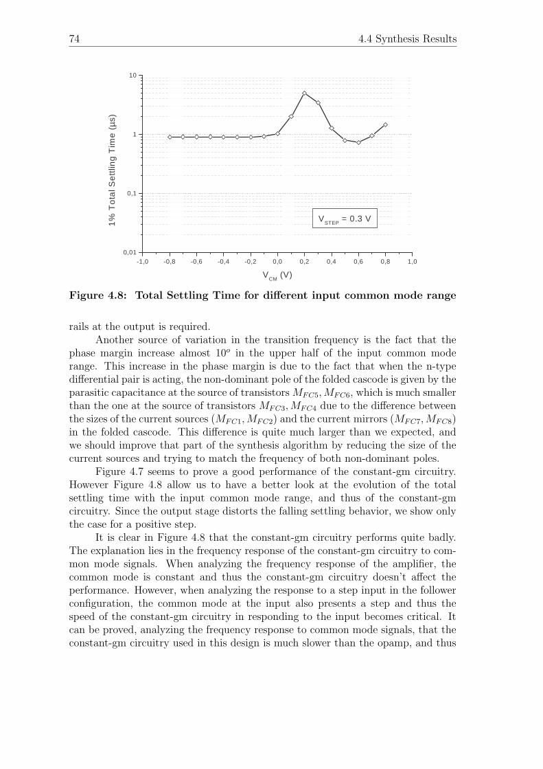
74 4.4 Synthesis Results
-1,0 -0,8 -0,6 -0,4 -0,2 0,0 0,2 0,4 0,6 0,8 1,00,01
0,1
1
10
VSTEP
= 0.3 V1%
To
tal S
ett
ling
Tim
e (
µs)
VCM
(V)
Figure 4.8: Total Settling Time for different input common mode range
rails at the output is required.Another source of variation in the transition frequency is the fact that the
phase margin increase almost 10o in the upper half of the input common moderange. This increase in the phase margin is due to the fact that when the n-typedifferential pair is acting, the non-dominant pole of the folded cascode is given by theparasitic capacitance at the source of transistors MFC5,MFC6, which is much smallerthan the one at the source of transistors MFC3,MFC4 due to the difference betweenthe sizes of the current sources (MFC1,MFC2) and the current mirrors (MFC7, MFC8)in the folded cascode. This difference is quite much larger than we expected, andwe should improve that part of the synthesis algorithm by reducing the size of thecurrent sources and trying to match the frequency of both non-dominant poles.
Figure 4.7 seems to prove a good performance of the constant-gm circuitry.However Figure 4.8 allow us to have a better look at the evolution of the totalsettling time with the input common mode range, and thus of the constant-gmcircuitry. Since the output stage distorts the falling settling behavior, we show onlythe case for a positive step.
It is clear in Figure 4.8 that the constant-gm circuitry performs quite badly.The explanation lies in the frequency response of the constant-gm circuitry to com-mon mode signals. When analyzing the frequency response of the amplifier, thecommon mode is constant and thus the constant-gm circuitry doesn’t affect theperformance. However, when analyzing the response to a step input in the followerconfiguration, the common mode at the input also presents a step and thus thespeed of the constant-gm circuitry in responding to the input becomes critical. Itcan be proved, analyzing the frequency response to common mode signals, that theconstant-gm circuitry used in this design is much slower than the opamp, and thus

4. Hierarchical Automated Synthesis 75
410p 4,1n 41n 410n1k
10k
100k
1M
10M
VCM
(V) :
-0.7
0.0
+0.7
f T (
Hz)
IREF
(A)
30
45
60
75
90
Ph
ase
Ma
rgin
(º)
Figure 4.9: Transition frequency (fT ) and Phase Margin tuning overmore than 3 decades
the settling time suffers a noticeable delay, as seen in Figure 4.8. On section 4.5 wewill further analyze the constant-gm circuit and show how the speed performancecan be improved.
On the other hand, Figure 4.8 shows that when these undesirable effects don’thinder the performance, the opamp complies with the 1µs total settling time speci-fications precisely. This proves the achievement of a major goal of this work, sincewe were able to automatically design a complex opamp cell that achieves the desiredcharacteristics.
One final remark goes to the extremely high value achieved for the DC gain.This is explained by several factors: a) there are three gain stages (two in the inputstage and one in the output stage), b) the output stage gain is enhanced by thetransconductance multiplication effect, c) these values correspond to operation witha purely capacitive load, in which case the output stage gain is maximum, d) we aretaking full advantage of the high gain achievable in the weak and moderate inversionregions. Nevertheless, it is expected to have smaller values in the experimentalprototypes due to presence of parasitic and unmodelled effects in the transistoroutput conductance.
We will now explore the reusability of this cell by exploring the performancetuning using the input bias current.
4.4.2 Opamp Performance Tuning
Figure 4.9 shows the first analysis of the reusability capabilities of the opampcell. The gain bandwidth product is tuned over more than 3 decades. From thedesign point (IREF = 41nA) we can go down working in deeper weak inversion.The figure shows the tuning down to IREF = 410pA, but there is no reason thatprevent us from going even further until leakage currents limit us. Regarding higher

76 4.4 Synthesis Results
-1,0 -0,8 -0,6 -0,4 -0,2 0,0 0,2 0,4 0,6 0,8 1,010k
100k
1M
10M
IREF
(nA) :
0.41
1.3
4.1
13
41
130
f T (
Hz)
VCM
(V)
-1,0 -0,8 -0,6 -0,4 -0,2 0,0 0,2 0,4 0,6 0,8 1,050
60
70
80
Ph
ase
Ma
rgin
(º)
Figure 4.10: Transition frequency and phase margin tuning as a functionof the input common mode
gain bandwidth product, we can’t go much higher than a decade or less, since thecell will start to have problems with the low supply voltage as transistors start toenter strong inversion operation, and thus, all the advantages of moderate and weakinversion for performance tuning, seen in section 3.2.1, won’t hold anymore.
Figure 4.9 shows the tuning for three different common mode voltages. We seea good performance, as expected, as the three curves are superposed along the wholetuning range in the gain bandwidth product and the 10o difference, seen on Figure4.7, also holds along the tuning range. Except for the last value, where the highersaturation voltage of the differential pair sources forces the constant-gm circuitryto act for VCM = 0.0V and the effect seen for high input common mode appears inthat curve.
The good response of the gain-bandwidth product with the input commonmode range in the whole tuning range, can be better appreciated in Figure 4.10. Itis clear that a constant small signal behavior is achieved along the input commonmode range in every tuning point. The transition from the p-type differential pairto the n-type differential pair, is also clearly visible in the phase margin, sincethe increase in it appears for lower input common mode range as the bias currentaugment.
We see also, how the saturation voltage of the output stage transistor Mbaffects the gain bandwidth product for the higher bias current because of the strongerinversion operation of that tuning point, as we commented above. This, can alsobe seen in the phase margin, which noticeably drops at higher common mode levelswhen operating in stronger inversion. This can be explained because the current

4. Hierarchical Automated Synthesis 77
0,41 4,1 41 4100,1
1
10
100
1000
VSTEP
= 0.3 V
VCM
:
-0.7 V
0.0 V
+0.7 V1
% T
ota
l Se
ttlin
g T
ime
(µs
)
IREF
(nA)
Figure 4.11: Total Settling Time tuning for three different input commonmodes where the constant-gm circuitry doesn’t affect the performancegreatly.
mirror Mc,Mb at the output stage no longer can be considered as a mirror withgain k, since transistor Mb is working in the linear region. Thus, gmmult has amuch lower value yielding lower NDP0 ratios, and an overall bad performance ofthe output stage.
In Figure 4.11 we see how we can tune our settling behavior from about 300nsup to 100µs. The higher phase margin of the upper part of the input common moderange, reflects on faster settling behavior, except for IREF above 41nA where thelack of dynamic range due to the higher saturation voltages of transistors hindersthe performance. Also, at IREF = 130nA the constant-gm circuitry activates belowVCM = 0V , and thus, the settling behavior suffers the consequences of its slowerresponse.
In spite of the problems described above, the performance is in excellent agree-ment with the expected results. For example, we are able to tune the settlingresponse of our amplifier to 100µs, using IREF = 0.41nA, and thus, reducing thecurrent consumption over two orders of magnitude.
One last plot regarding the tuning of the opamp cell is presented in Figure4.12. Here we see the effect of both problems described above. The slower responseof the constant-gm circuitry and the lack of dynamic range at the output stage dueto the stronger inversion operation when tuning for faster settling times.
Nevertheless, this section has proved another major goal of this work. If wedesign our amplifier to work between weak and moderate inversion, then we cantune our amplifier over several decades, all the way down into deep weak inversionwithout loss of performance.
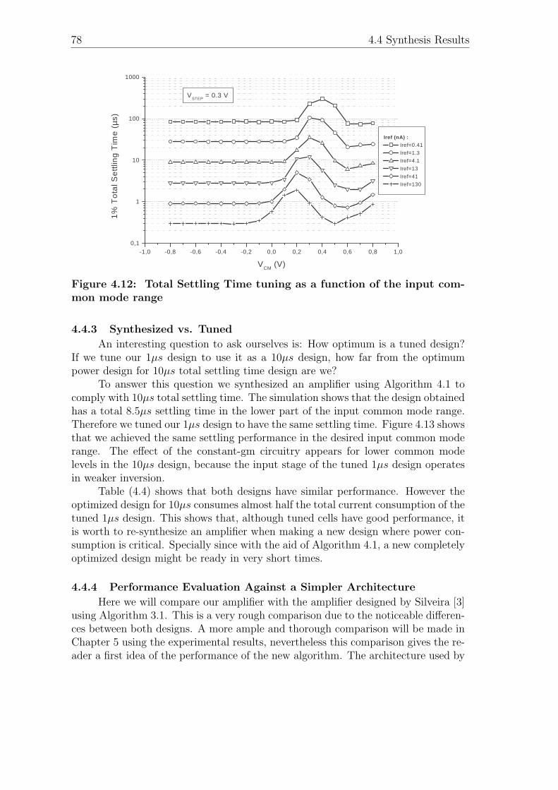
78 4.4 Synthesis Results
-1,0 -0,8 -0,6 -0,4 -0,2 0,0 0,2 0,4 0,6 0,8 1,00,1
1
10
100
1000
VSTEP
= 0.3 V
Iref (nA) :
Iref=0.41
Iref=1.3
Iref=4.1
Iref=13
Iref=41
Iref=130
1%
To
tal S
ett
ling
Tim
e (
µs)
VCM
(V)
Figure 4.12: Total Settling Time tuning as a function of the input com-mon mode range
4.4.3 Synthesized vs. Tuned
An interesting question to ask ourselves is: How optimum is a tuned design?If we tune our 1µs design to use it as a 10µs design, how far from the optimumpower design for 10µs total settling time design are we?
To answer this question we synthesized an amplifier using Algorithm 4.1 tocomply with 10µs total settling time. The simulation shows that the design obtainedhas a total 8.5µs settling time in the lower part of the input common mode range.Therefore we tuned our 1µs design to have the same settling time. Figure 4.13 showsthat we achieved the same settling performance in the desired input common moderange. The effect of the constant-gm circuitry appears for lower common modelevels in the 10µs design, because the input stage of the tuned 1µs design operatesin weaker inversion.
Table (4.4) shows that both designs have similar performance. However theoptimized design for 10µs consumes almost half the total current consumption of thetuned 1µs design. This shows that, although tuned cells have good performance, itis worth to re-synthesize an amplifier when making a new design where power con-sumption is critical. Specially since with the aid of Algorithm 4.1, a new completelyoptimized design might be ready in very short times.
4.4.4 Performance Evaluation Against a Simpler Architecture
Here we will compare our amplifier with the amplifier designed by Silveira [3]using Algorithm 3.1. This is a very rough comparison due to the noticeable differen-ces between both designs. A more ample and thorough comparison will be made inChapter 5 using the experimental results, nevertheless this comparison gives the re-ader a first idea of the performance of the new algorithm. The architecture used by
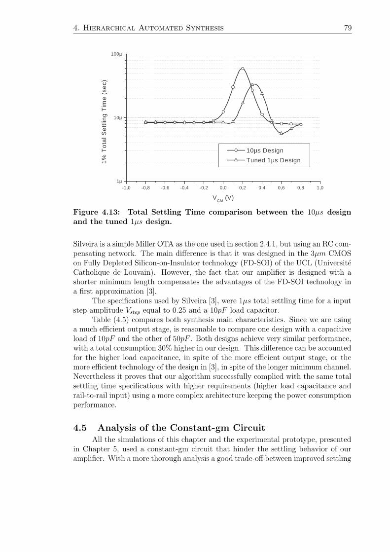
4. Hierarchical Automated Synthesis 79
-1,0 -0,8 -0,6 -0,4 -0,2 0,0 0,2 0,4 0,6 0,8 1,01µ
10µ
100µ
10µs Design
Tuned 1µs Design1%
To
tal S
ett
ling
Tim
e (
sec)
VCM
(V)
Figure 4.13: Total Settling Time comparison between the 10µs designand the tuned 1µs design.
Silveira is a simple Miller OTA as the one used in section 2.4.1, but using an RC com-pensating network. The main difference is that it was designed in the 3µm CMOSon Fully Depleted Silicon-on-Insulator technology (FD-SOI) of the UCL (UniversiteCatholique de Louvain). However, the fact that our amplifier is designed with ashorter minimum length compensates the advantages of the FD-SOI technology ina first approximation [3].
The specifications used by Silveira [3], were 1µs total settling time for a inputstep amplitude Vstep equal to 0.25 and a 10pF load capacitor.
Table (4.5) compares both synthesis main characteristics. Since we are usinga much efficient output stage, is reasonable to compare one design with a capacitiveload of 10pF and the other of 50pF . Both designs achieve very similar performance,with a total consumption 30% higher in our design. This difference can be accountedfor the higher load capacitance, in spite of the more efficient output stage, or themore efficient technology of the design in [3], in spite of the longer minimum channel.Nevertheless it proves that our algorithm successfully complied with the same totalsettling time specifications with higher requirements (higher load capacitance andrail-to-rail input) using a more complex architecture keeping the power consumptionperformance.
4.5 Analysis of the Constant-gm CircuitAll the simulations of this chapter and the experimental prototype, presented
in Chapter 5, used a constant-gm circuit that hinder the settling behavior of ouramplifier. With a more thorough analysis a good trade-off between improved settling

80 4.5 Analysis of the Constant-gm Circuit
10µs Design Tuned 1µs DesignITOT (µA) 0.58 1.18fT (kHz)@VCM = −0.5V 88.3 120.3@VCM = 0.0V 87.1 118.4@VCM = +0.5V 88.2 121.7PM(o)@@VCM = −0.5V 68.5 63.9@VCM = 0.0V 68.6 64@VCM = +0.5V 71.8 72.5SR(mV/µs)@VCM = −0.7V 51 51@VCM = 0.0V 51 52@VCM = +0.7V 59 52
Table 4.4: Comparison between the 10µs design and the tuned 1µs design.
[3] This workSettling Specification (µs) 1 1Technology 3µm FD-SOI 0.8µm BulkLoad Cap. (pF) 10 50ITOT (µA) 7.05 10.33GainDC(dB) 82 167fT (MHz) 0.75 0.85PM(o) 68 58SR(V/µs) 0.59 0.59
Table 4.5: Comparison between our amplifier and the one designed in [3]using Algorithm 3.1 with a simple Miller OTA.
behavior and increased consumption is presented. Regrettably, the improvement inthe settling behavior could not be achieved before the prototype was fabricated andthus, the ideas discussed in this section could not be verified experimentally.
4.5.1 Open Loop Transfer
On Figure 4.14 we recall (see section 3.3.1) the constant-gm circuit loop thatfixes the total transconductance equal to the transconductance of the differentialpair TP,ref . If we want to analyze the dynamics of the loop we must open it toobtain an expression for the open loop transfer. We choose to open at the inputof the current source of differential pair TN . Thus, input and output signals aredefined (VIN , VOUT ) for the open loop transfer.

4. Hierarchical Automated Synthesis 81
Figure 4.14: Constant-gm circuit loop.
We will write this open loop transfer as:
VOUT
VIN
=VOUT
∆i
∆i
VIN
(4.34)
where ∆i is the sum of all the differential currents iN , iP and iREF . This sumis performed by the folded cascode circuit and thus it has a frequency response,analyzed in section 4.3.2, that we will note F (s). According to the input stagesynthesis algorithm (see Algorithm 4.2) the poles introduced by F (s) lie above thetransition frequency of the opamp, and thus, we will suppose that they don’t affectthe frequency response of the loop. ∆i can be written as,
∆i = (iN + iP + iREF )F (s) (4.35)
where the sum of the differential currents equals zero in regime. During the transientresponse to a signal in VIN the only differential current that changes is iN , thus, wecan further expand equation (4.34) as
VOUT
VIN
=VOUT
∆i
inVIN
F (s) (4.36)
where in is the signal current in iN due to VIN .The first term is determined by the output impedance of the folded cascode
circuit and the gate capacitance of the current source transistor of the differentialpair TN . Thus, the expression is
VOUT
∆i= − 1/goFC
1 + s/ωpo
where ωpo =goFC
Cg3
(4.37)
goFC is the output conductance of the folded cascode and Cg3 is the total output

82 4.5 Analysis of the Constant-gm Circuit
capacitance, mostly dominated by the gate capacitance of the current source.The second term is less trivial. We got an increase in the bias current of the
differential pair TN given by gm3VIN , where gm3 is the transconductance of thecurrent source. This increase of bias current will increase gm1, which in turn willincrease in. Continuing with a small signal model we will write this term as
inVIN
= kV gm3 (4.38)
where kV reflects the increase of differential current due to V for a small increase inthe bias current. It can be seen that this term can be written as
kV =1
2(gm/ID)1 V (4.39)
where (gm/ID)1 is the (gm/ID) ratio of the n-type differential pair. In our case,since V = 10mV , kV = 0.09. Finally, the complete open loop transfer function is
VOUT
VIN
= −kV
gm3
goFC
1 + sωpo
F (s) (4.40)
which can be rewritten as
VOUT
VIN
= − A0
1 + sA0
ωT
F (s) (4.41)
where
A0 = kVgm3
goFC
(4.42)
ωT = kVgm3
Cg3
(4.43)
which is a very reasonable result, since the gain-bandwidth product of our transferis dominated by the total output capacitance of the folded cascode.
Using this equations, the current source transistors of the n-types differentialpairs can be sized. Here, we face a trade-off between speed and the length of thetransistors, since if we size it to have minimum length, Cg3 will be minimum, butunacceptable common mode rejection ratios are obtained. Also we must take intoaccount the position of the poles in F (s) since the loop could become unstable.
4.5.2 Bias Current Monitor
Another part of the constant-gm circuit that slows down the performance is thebias current monitor circuit. This circuit (see section 3.3.1 and Figure 3.7) monitorsthe bias current of the p-type differential pair in the input stage and generates areplica for the differential pair TP in the constant-gm circuit. In Figure 4.14 this

4. Hierarchical Automated Synthesis 83
-1,0 -0,8 -0,6 -0,4 -0,2 0,0 0,2 0,4 0,6 0,8 1,00,0
500,0n
1,0µ
1,5µ
2,0µ
2,5µ
3,0µ
3,5µ
4,0µ
4,5µ
5,0µ
5,5µ
6,0µ
Constang-gm Circuit:
Fabricated
New Version1
% T
ota
l Se
ttlin
g T
ime
VCM
(V)
Figure 4.15: Settling time as a function of the input common mode withthe redesign of the constant-gm circuit
circuit is represented by the voltage controlled current source IBP (VCM).This circuit, formed by 3 current mirrors and a replica of the differential pair,
has to be much faster than the rest of the constant-gm circuit. Then, the currentmirrors will be sized to assure that the frequency doublets they introduce, lie atmuch higher frequencies.
The problem with this circuit is that when IBP (VCM) tends to 0 all the currentmirrors leave the saturation region and an unacceptable delay is introduced. Thus,a constant “bias” current has to be added in all these current mirrors in order tokeep them always on the saturation region. Obviously this solution will increase thetotal consumption. Therefore, the trade off will be between the amount of currentinvested and the error in the copy of the current due to the maximum acceptablesize for the mirrors transistors.
4.5.3 Redesign of the Constant-gm Circuit
Taking into consideration the limitations considered in this section, we rede-signed the current source transistor of the n-type differential pairs and the currentmirrors of the bias current monitor. The size of the current source is W/L = 2/8and the size of the current mirrors is W/L = 2/6. The added bias current is 100nA.
A simulation using this redesign, which is far from being optimized, yields theresults shown in Figure 4.15. It is clear that a very acceptable result was obtained,since the total variations due to the transition between differential pairs is less than500ns compared to almost 5µs in the previous design. In this redesign, the totalcurrent consumption was increased only 300nA which is less than the 5% of thetotal previous current consumption.
84 4.6 Conclusions
Further analysis and simulations are due here, and certainly is a topic of futureresearch.
4.6 ConclusionsA new hierarchical automated synthesis algorithm was presented. This algo-
rithms successfully synthesizes a rail-to-rail opamp cell to comply with a given totalsettling time with minimum power consumption.
The hierarchical approach allow us to independently synthesize each stage,decoupling the high level specifications from the actual implementation of each stage.This is a major advantage since we can use different architectures in the input stage,for example, changing only the input stage synthesis.
The results obtained in section 4.4.1 proves that the developed algorithm suc-cessfully complies with the total settling time specification, and comparisons withother designs from the literature presented in Chapter 5, will show that this is trulyachieved with optimum consumption. A first example of the good power consump-tion achieved was presented in section 4.4.4 with a design using Algorithm 3.1, inspite of the notorious differences in both designs.
Another mayor achievement was presented in section 4.4.2, where we prove thefeasibility of tuning the performance of the opamp cell through the bias current. Theobtained results showed that we can tune the settling time characteristic of the cellfor over more than 3 decades. Nevertheless, section 4.4.3, showed that, expectedly,this “tuned” designs don’t have optimum power consumption. Thus, regarding newdesigns, a trade-off between reuse with sub-optimum power consumption and quickre-synthesis of new optimum designs is present.
Finally, the two weakness seen on the performance of this cell have two differentsources. One is a problem with the rail-to-rail input stage architecture, which we usein spite of its poor frequency response for common mode signals. The constant-gmcircuit was analyzed and redesigned in section 4.5 with a significant improvement inthe settling behavior. Nevertheless, recently, a new rail-to-rail input stage with allthe desirable characteristics of the one used here (constant-gm, robust and universal)but also with constant slew rate (large signal behavior) and a feed-forward schemewas presented [6]. Then, taking advantage of the superior performance of thislast architecture, we could redesign our amplifier with this new input stage bychanging the input stage synthesis to suit the different architecture; and this is onefundamental achievement, since this algorithm has a great degree of independencefrom the architecture used to implement each stage. The other problem in theperformance is that the current mirrors of the output stage were synthesized tooperate at almost strong inversion, and thus we end up with an output stage witha loss of 150mV in the total output swing. This was done so, because the synthesisalgorithm designed the current mirrors based only on their frequency response. Asalways, the algorithm can be improved, and the inclusion of a minimum allowable(gm/ID) ratio for the current mirrors could be easily added.
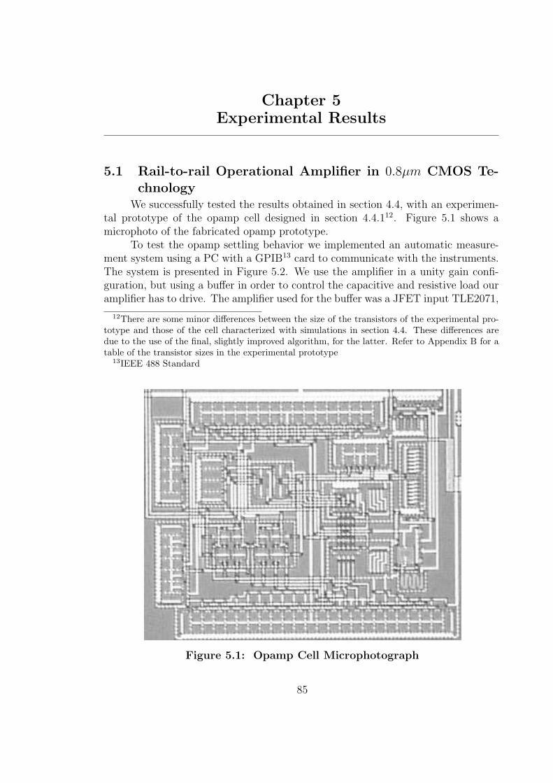
Chapter 5Experimental Results
5.1 Rail-to-rail Operational Amplifier in 0.8µm CMOS Te-chnology
We successfully tested the results obtained in section 4.4, with an experimen-tal prototype of the opamp cell designed in section 4.4.112. Figure 5.1 shows amicrophoto of the fabricated opamp prototype.
To test the opamp settling behavior we implemented an automatic measure-ment system using a PC with a GPIB13 card to communicate with the instruments.The system is presented in Figure 5.2. We use the amplifier in a unity gain confi-guration, but using a buffer in order to control the capacitive and resistive load ouramplifier has to drive. The amplifier used for the buffer was a JFET input TLE2071,
12There are some minor differences between the size of the transistors of the experimental pro-totype and those of the cell characterized with simulations in section 4.4. These differences aredue to the use of the final, slightly improved algorithm, for the latter. Refer to Appendix B for atable of the transistor sizes in the experimental prototype
13IEEE 488 Standard
Figure 5.1: Opamp Cell Microphotograph
85

86 5.1 Rail-to-rail Operational Amplifier in 0.8µm CMOS Technology
!
"
#
$
%& '(
'(
()
(
$*
*+,
-)--
Figure 5.2: Settling time automatic measurement system
which has capacitive load of approximately 15pF at the input.The signal generator used was the HP3245A, which we used to generate a
square wave signal at different input common modes. Both input and output signalswere registered with a 500MHz, 5GS/s Oscilloscope (Tektronix TDS3052). Finally,to precisely bias the opamp (D.U.T.: Device Under Test) over all the tuning range,we use the Semiconductor Analyzer HP4155A.
Then using the GPIB bus we could measure the settling behavior of the opampalong the input common mode range for every point of the tuning range.
Using this system, we measured the total settling time at 5% for a 0.3V stepamplitude. We add a capacitive load CL = 33pF which, along with the buffer inputcapacitance, completes CLtot ' 48pF . Figure 5.3 shows the results of the mea-surements. A good performance was obtained, and we can see that the expectedbehavior of the constant-gm circuit is clearly present. We can see also that the sett-ling behavior for the last tuning point (IREF = 120nA) didn’t achieve the expectedperformance.
To have a better evaluation of the settling behavior of the opamp, Figure 5.4compares the settling time over the whole tuning range between the simulation of thesynthesis result and the measurements made with the experimental prototype. Herewe see that the prototype is a bit slower compared to the simulations. Neverthelessa good agreement is achieved between both results, except for the last tuning point,as anticipated by Figure 5.3.
As we mentioned in section 4.4.2, in this last tuning point, the amplifier is inthe limits of its capabilities, as critical transistors start to enter strong inversion, andthe reusability hypothesis don’t hold any longer. The experimental prototype seemsto have a degraded frequency response, since the step responses are more oscillatorythan expected, particularly for this last tuning point. This might be caused bythe parasitic capacitances introduced by the metal connections in sensitive nodes.According to the circuit extracted from the layout, this parasitic capacitances are a

5. Experimental Results 87
-1,0 -0,8 -0,6 -0,4 -0,2 0,0 0,2 0,4 0,6 0,8 1,0100n
1µ
10µ
100µ
1m
IREF
:
0.4
1.2
4
12
40
120
5%
To
tal S
ett
ling
Tim
e (
sec)
VCM
(V)
Figure 5.3: Total settling time tuning as a function of the input commonmode range
0,4 4 40 400100n
1µ
10µ
100µ
1m
Exp. VCM
Sim.
-0.7
0.0
+0.7
5%
To
tal S
ett
ling
Tim
e (
sec)
IREF
(nA)
Figure 5.4: Comparison between the simulated and experimental totalsettling time tuning for three different input common modes

88 5.1 Rail-to-rail Operational Amplifier in 0.8µm CMOS Technology
100n 1µ 10µ 100µ100n
1µ
10µ
100µ
1m
VCM
(V) :
-0.7
0.0
+0.7
5%
To
tal S
ett
ling
Tim
e (
sec)
Total Consumption (A)
Figure 5.5: Settling time as a function of the total quiescent currentconsumption.
few tens of fF which are in the order of the drain junction parasitic capacitancescalculated in the synthesis algorithm. Therefore, the position of the non-dominantpoles could vary significantly. This is visible in the simulation of the extractedamplifier including the parasitic capacitances of the metal connections. The circuitpresented a phase margin of only 55o compared to the same extracted circuit withoutthose metal connections parasitic capacitances, which has a phase margin above 60o.To prove that this is the reason for the minor oscillations observed in the settlingbehavior, we measured the settling time with a load capacitance CL = 22pF , whichcompletes a total load of CLtot ' 37pF . The oscillations where almost completelygone, which means that, indeed, our amplifier has a degraded phase margin withrespect to the simulations made.
Figure 5.5 shows the amplifier’s speed-power trade-off. We can appreciatethat the amplifier is limited up to 1µs of total settling time, and also, that forslow settling times we obtain really low power consumptions. Two remarks are duehere. One, as we showed in section 4.4.3, the power consumption in a particulartuning point could be greatly improved if we synthesize the amplifier specificallyfor that point. Two, in the slowest tuning point showed (100µs), the consumptionis noticeable above the expected value of approximately 100nA. This is becausethe bias circuit that generates the two constant input voltages for the constant-gmcircuit differential pairs (see section 3.3.1), consumes 60nA independently of the biascurrent. This consumption is negligible in the 1µs settling time design, but almostequals the rest of the current consumption in this last tuning point.
Table (5.1) presents a comparison between the simulated and experimentalresults of the opamp cell in its design point (IREF = 40nA). We choose three

5. Experimental Results 89
VCM(V ) -0.7 0.0 +0.7Sim. Meas. Sim. Meas. Sim. Meas. Notes
IDD(µA) 9.68 9.83 10.34 10.17 10.96 10.43A0(dB)) 167 > 120 167 > 120 167 > 120 1, RL = ∞tset(µsec)5% (rise) 0.91 0.91 1.02 0.81 0.95 1.13 2, CL = 48pFtset(µsec)5% (fall) 1.9 4.9 2.19 5.8 1.64 1.7 2, CL = 48pFSR(V/µs) (rise) 0.42 0.48 0.45 0.53 0.52 0.38 CL = 48pFSR(V/µs) (fall) 0.32 0.45 0.39 0.57 0.30 0.38 CL = 48pFOffset (mV) 8.6 8.1 16.7 3Area (mm2) 0.083
1: Measured in a previous version of the prototype.2: Input step has 0.3V amplitude.
3: Measured in follower configuration.
Table 5.1: Opamp Cell characteristics.
different common mode levels where we can appreciate the behavior of the opampwhere only the p-type differential pair is acting (VCM = −0.7V ) and before and afterthe undesirable effect of the constant-gm circuit (VCM = 0.0V and VCM = +0.7V ).
The consumption is in excellent agreement with the expected results. As wesaw in Figure 5.4, the rise settling time also has an acceptable agreement. However,the settling response presents a more oscillatory response because of the degradedphase margin of the prototype, and although this effect is almost negligible in therise response, it has a serious impact on the fall settling behavior.
As we mentioned in section 4.4.1, the output stage has a known oscillatoryeffect in the fall settling due to the turn on delay of the current mirrors [3]. In thework by Silveira [3], this effect although undesired, didn’t had a severe consequencein the total fall settling time, because the fall slew rate was almost three timeshigher than the rise slew rate and the phase margin was 68o. In our work, both slewrates are approximately equal and most important, the phase margin is severelydegraded. In the lower half of the input common mode range, where we expectedto have over 60o we only have 55o. Then, the oscillations caused by the outputstage take a much longer time to extinguish yielding settling times between 5 and6 times longer than the rise settling. This is not the case in the upper half of theinput common mode range, where, although the phase margin is also degraded, weexpected to have almost 70o, due to the non-symmetrical behavior of the foldedcascode non-dominant poles, and we end up (always according to simulations) withapproximately 60o. Regarding the settling behavior there is no big difference if thephase margin is either 60o or 70o, and thus for VCM = +0.7V the settling timeagrees with the simulated results.
Measured offset values are acceptable, and a noticeable increase is appreciatedin the upper half of the input common mode range. This is not unexpected sincedifferent input stages are acting in each half of the input common mode range. Mo-

90 5.2 Comparison with other published results
-1,0 -0,8 -0,6 -0,4 -0,2 0,0 0,2 0,4 0,6 0,8 1,00,0
5,0m
10,0m
15,0m
20,0m
25,0m
30,0m
35,0m
40,0m
IREF
(nA) :
0.4
1.26
4
12.6
40
126
Off
set
Vo
ltag
e (
V)
VCM
(V)
Figure 5.6: Offset voltage as a function of the input common mode.
reover, not only each stage has different type of transistors, but also each differentialpair has a different load circuit. Figure 5.6 shows the offset voltage for different biascurrents. Once again, we see that the transition between each input stage is clearlya function of the reference current, hence is a function of the saturation voltage ofthe p-type differential pair current source.
5.2 Comparison with other published resultsIn this section we will compare the performance of our amplifier with other
published results.Several figures of merit have been presented to evaluate the speed-power trade-
off achieved by operational amplifiers. In reference [55] the gain-bandwidth dividedby the consumed power is used. However, it makes sense to include the load ca-pacitance in the trade-off. Therefore, references [7, 8] use the following figure ofmerit
FOMS
(MHz.pF
mW
)=
GBW.CL
power(5.1)
However, this figure only compares the small signal behavior of the amplifier.Therefor we will also use another figure of merit [8], that takes into account thelarge signal behavior of the speed-power trade-off in amplifiers using the slew rateinstead of the gain-bandwidth product,
FOML
(pF.V/µs
mW
)=
SR.CL
power(5.2)
where the average SR of the amplifier is taken.

5. Experimental Results 91
Power Load GBW PM SR FOMS FOML
(mW@VDD) (kΩ/pF ) (MHz) (o) (V/µs) (MHz.pFmW ) (pF.V/µs
mW )This work 0.021@2 ∞/50 0.85 > 55 0.47 2024 1119[3](1) 0.014@2 ∞/10 0.75 68 0.48 536 343[3](2) 0.048@2 10/22 1.4 50 1.15 642 527[5] [email protected] ∞/15 1.3 64 1 42 33[6] 4.8@3 0.56/33 17.5 60 16.27 93 72[7] 6.9@3 ∞/40 47 76 69 272 400[8] 2.45@3 ∞/300 10.4 63.7 3.5 1273 429
Table 5.2: Comparison of the performance of the Opamp Cell.
Table (5.2) presents the comparison of the performance of the opamp cellagainst several other published examples. Reference [3] presents the design of seve-ral amplifiers. Both examples used there, are amplifiers designed in 2µm FD-SOItechnology, which is considered [3] to be “comparable” with our 0.8µm bulk techno-logy. The first example taken its a simple Miller OTA designed for optimum powerconsumption using Algorithm 3.1. This is the same amplifier used for the compa-rison made in section 4.4.4, and we can appreciate that the most efficient outputstage allowed our design to out-perform the power efficiency of this design in spiteof our rail-to-rail input stage.
The second example from reference [3] is a Miller OTA with the same classAB output stage used in this work. This second amplifier was also designed foroptimum power consumption using an algorithm similar to Algorithm 4.3 that isgain-bandwidth driven. An interesting result is that, since the gain-bandwidth is1.4MHz, the optimum mirror gains found for this amplifier were approximatelythe same found in our design (h = 1, k = 8,m = 3). The difference is that theoptimizing algorithm used didn’t take jointly into account the internal and externalslew rates. Thus the algorithm “over-dimensioned” the output stage current, whilethe slew rate was determined by the input stage. This explains why our design hasa better figure of merit.
Reference [5] is an amplifier with constant-gm rail-to-rail input stage desig-ned for low-voltage operation, but with no special consideration for consumption.The design was made in 0.7µm standard CMOS technology and presents very si-milar gain-bandwidth and slew rate values. However this comparison shows howfar from optimum consumption a design can be, if consumption is not taken intoconsideration during design.
Reference [6] presents an amplifier with a constant-gm, constant slew rate in-put stage that complies with all the desirable characteristics seen in section 3.2.2.As we mentioned in section 4.6, this input stage don’t have restrictions in its opera-ting frequency range, since it uses a feed-forward scheme. What is more interestingabout this input stage is that it works with approximately the same number of co-pies of the input stage bias current used in the input stage used in this work. Thusit is feasible of being used with our algorithm, since it wouldn’t jeopardize our powerefficiency.

92 5.3 Conclusions
The opamp designed in reference [6] includes a class AB output stage that givesthe amplifier high-drive capabilities and makes the design appropriate for videoapplications. Nevertheless, both figures of merit shows that the design is quitefar from begin optimum in a power consumption sense, in spite of some minorconsiderations mentioned by the authors and its drive capabilities.
Reference [7] presents a three-stage opamp implemented in 0.6µm n-well CMOStechnology. The work is focused in the development of embedded frequency compen-sation networks. The amplifier achieves high-bandwidth and fast slewing figures fora capacitive load of 40pF . The authors accurately report a good power efficiencyusing the figure of merit presented in equation (5.1). Therefore, we see anotherexample of the truly optimum power design obtained with the algorithm developedin this work.
Finally, we took the amplifier designed in reference [8] to compare our workwith an amplifier specially designed to drive heavy capacitive loads (300pF ) and,therefore, prove that our higher figures of merit are not accounted only for therelatively high capacitive load driven by our output stage. We can see in Table (5.2)that our amplifier still has a better power efficiency performance.
5.3 ConclusionsThis chapter has shown the experimental results of the reusable opamp cell
synthesized in Chapter 4. Excellent agreement between the settling time specifica-tions and the measurements was obtained in spite of the expected effect due to theconstant-gm circuit.
The power-speed trade-off can be successfully tuned over more than 3 deca-des, beyond a 100µs settling time design that has total current consumption below180nA. A degraded phase margin, partially due to small parasitic capacitance insensitive nodes of the circuit, prevent us from achieving settling times below 1µs,nevertheless the cell proved to have excellent tuning capabilities.
We took the usual figures of merit to measure and compare the power-speedtrade-off against several examples from the literature. We could appreciate that ourdesign achieves very high figures of efficiency, which proves the true optimizationachieved by the synthesis algorithm.
On the next chapter we will review the conclusions and goals of the wholework, along with some open lines of future research.

Chapter 6Conclusions
This thesis presented the development of an automatic synthesis algorithmintended for micropower operational amplifiers. This algorithm is based in previouswork on this subject that originate with the (gm/ID) methodology proposed anddeveloped by Prof. Paul Jespers and the staff of the Microelectronics Laboratory,at the Universite Catholique de Louvain (UCL).
The basic automatic synthesis algorithm developed by the UCL, and presen-ted in Chapter 2 (Algorithm 2.1), is gain-bandwidth driven and has been used tointroduce the application of the (gm/ID) methodology and the idea of design spaceexploration (Algorithm 2.2) which has been further improved in this work. This ideaallows us to obtain optimum combinations of the (gm/ID) ratios not only regardingspeed-power trade-offs but in any sense needed by the designer. We have presentedhere how to apply this algorithms using a single piece, continuous MOSFET modelthat allow us to explore different trade-offs in the selection of several, previouslyunexplored, design variables. Nevertheless, these algorithms were based in amplifierspecifications, which prevents us from achieving automatic synthesis starting fromspecifications at an application level.
The work done by Prof. Silveira [3] provided a mean to transit from high levelspecifications (settling time) to the amplifier specifications and, then to transistorsizing using the (gm/ID) methodology. The resulting power optimization algorithm(Algorithm 3.1) was applied to a simple RC compensated Miller amplifier, andseveral results were obtained, particularly, the proof of the existence of an optimumconsumption design point. Also, Prof. Silveira [3] presented a new approach for thedesign of a class AB output stage that exploits a transconductance multiplicationeffect. A need, then, to extend the power optimization algorithm to include amplifierarchitectures as this class AB output stage and rail-to-rail input stages, was ofparticular interest in the field of analog design automation in low-voltage, powercritical systems.
In this work we could successfully fill this need by developing a hierarchicalsynthesis algorithm (Algorithm 4.1) based on the power optimization algorithmpresented by Silveira [3], but decoupling in a great degree the synthesis of eachstage with the high level synthesis of the amplifier. This allows us to use the samealgorithm, with minor changes, for an amplifier with a different input or outputstage architecture.
To further advance in the field of analog design automation, we explore andreview the options in analog design reuse, including a brief review of technologymigration. We proved that an amplifier cell designed to operate in weak or near-weakinversion, can have its speed-power trade-off tuned over several decades without lossof performance in other aspects. This was verified in an experimental prototype
93

94
designed using the algorithm developed in this work.The problems presented by the prototype were mostly due to problems with
the selected architectures. Specially with the selected rail-to-rail input stage, whichfailed to perform as expected. After further analysis and redesign of this stage,an important improvement in the settling behavior was achieved. However, thisimprovement could not be included in the fabricated prototype. A second problem,appear due to the sensitivity of some nodes to parasitic capacitances of such smallvalues as a few tens of fF . This can be improved with a more careful layoutdesign. Nevertheless, the loss of performance caused by this problem, could havebeen negligible, except for the third and last problem which we encountered.
This last issue, regards a known oscillatory effect of the class AB output stage.Silveira [3] suggested an auxiliary circuit to overcome this problem. However, itdidn’t work in our design and it was finally dropped from the prototype. An alter-native was briefly and unsuccessfully searched, and finally the circuit was fabricatedwith the known deficiency, since its solution was not a critical objective of this work.
In summary, the main results of this work are:
• It thoroughly reviewed the simple automatic synthesis algorithms for ampli-fiers, applying a continuous MOSFET model that uses simple single-pieceequations.
• It presented and experimentally verified the possibility of performance tuningthrough the bias current in amplifiers.
• It has verified not only the existence of an optimum compensation capacitancein Miller amplifiers, but also, to our best knowledge, a new expression todirectly estimate its value has been developed. Previous algorithms sweptpredefined values of the capacitance and synthesized the whole amplifier ineach of them to obtain the optimum, with the obvious penalty paid in theneeded processing time.
• It presented a new approach to develop a hierarchical automatic synthesisalgorithm that allows the designer to easily decouple the high level synthesisfrom each stage synthesis. The approach was applied in the development of ahierarchical algorithm based on the settling time driven algorithm presentedby Silveira [3], for a rail-to-rail amplifier with a power efficient class AB outputstage.
• Besides some problems encountered with the performance of the architecture,the synthesis algorithm was successfully verified with an experimental pro-totype that complies with the design specifications with truly optimal powerconsumption.
• Additional results were obtained in the extension of the design space explora-tion algorithm (Chapter 2) and the design methodology for the cascode biascircuit presented in Appendix A.

6. Conclusions 95
Future Work
In order to further optimize the resulting amplifier, the constant speed per-formance over the whole input common mode range could be improved extendingthe analysis of the constant-gm circuit. Alternatively, the use of recently proposedrail-to-rail input stages [6] that overcomes the deficiencies of the selected input stagecould be considered.
Of course, there is also still much to do in the direction of automatic ana-log design. The hierarchical approach presented here, should be extended to otheramplifier architectures, to prove its major advantages in power consumption opti-mization. Also, it would be interesting to explore the use of these opamp designtechniques and the reuse concept in a system-level example, to show the poweroptimization capabilities in a whole system.

96

Appendix ALow-Voltage Cascode Bias Transistor Design
The summing circuits present in the input stage of the opamp, are implementedwith a folded cascode stage. In these circuits, two voltages must be generated inorder to bias the cascode transistors. Figure A.1 shows the circuit used, where M2is the cascode transistor, M1 is the transistor to be cascoded and M3 is a diode-connected transistor used to bias M2. An equivalent pMOS circuit is used to biasthe pMOS cascode transistors. This circuit was first proposed in [56] and a firststudy of its design, using EKV model, can be found on [57].
The basic idea proposed in [57], is to fix the drain-source voltage of M1 closeto the drain-source saturation voltage by choosing an adequate operation point forM3 as a function of the operating point of M1 and M2.
In [57], transistors M1 and M2 were supposed to be working in strong inversion(M1) and weak inversion (M2) and the EKV expressions on those limits were usedto design M3. Here, as far as we know, we propose a new set of design equationsbased on a continuous model valid in all region of operation (ACM), which, hence,doesn’t depend on the operating point of the transistors.
If Ib is the bias current through M2 and Ib/k is the bias current through M3we can define a first relation between the operating point of M2 and M3 usingequation (2.3)
ID2
ID3
= k =if2(W/L)2
if3(W/L)3
(A.1)
Figure A.1: Cascode transistor bias.
97

98
then
if3 =if2(W/L)2
k(W/L)3
(A.2)
Recalling equation (2.6), we can write the pinch-off voltage for transistors M2and M3 as:
VP2 = VD1 + φT f(if2) (A.3)
VP3 = φT f(if3) (A.4)
where
f(if ) =√
1 + if − 2 + ln(√
1 + if − 1)
(A.5)
In equation (A.3) VD1 is the drain voltage of M1 and, as we said, the criteriumwill be to fix it close to the saturation voltage. Using equation (2.8), in the caseε = 1%, we can define VD1 as
VD1 = VDSsat1 + ∆Vmargin = φT
(√1 + if1 + 3
)+ ∆Vmargin (A.6)
where ∆Vmargin defines how close we want the drain voltage to the saturation voltage.Since VG2 = VG3, then VP2 = VP3 and combining equations (A.3) to (A.6)
we obtain the following expression that relates the inversion factor of the threetransistors:
√1 + if3 −
√1 + if2 −
√1 + if1 + ln
(√1 + if3 − 1√1 + if2 − 1
)= 3 +
∆Vmargin
φT
(A.7)
Then, using equations (A.2) and (A.7) we can develop the following methodto design transistor M3. First, we define ∆Vmargin and using equation (A.7) weobtain the inversion level for transistor M3. Then, we define factor k according tothe current budget, and using equation (A.2), we obtain the (W/L)3 ratio.
It is worth noticing that both equations used, are completely independent ofthe technology used, and so, become powerful design tools for this circuit.
The criterium used in this work was to consider ∆Vmargin = 4φT

Appendix BSize of Transistors in the Experimental Prototype
Differential Pair Output StageW 3 L 3 M (gm/ID) W 3 L 3 M (gm/ID)
C.M. 1 7.7 20 15 Ma 13.6 1 1 15D.P. 2 8.9 10 1 18 Mf 11.2 1 1 15Folded Cascodes Mb 2 1 8.5 12.3
W 3 L 3 M (gm/ID) Mc 2 1 1 12.3MFC1 7.7 20 4 15 Md 2 1 3 21.7MFC3 2.5 2 1 22.8 Me 2 1 1 21.7MFC5 4.5 2 1 21.9 Mos1 4.1 10 1 3.4MFC7 2 3.2 1 16.1 Mos2 4.1 10 2 3.4
1: Current Mirrors.2: Differential Pairs Transistors.
3: W and L in µm.
Table B.1: Transistors sizes in the experimental prototype. M is thenumber of parallel transistors.
99

100

Bibliography
[1] F. Silveira, D. Flandre, and P. G. Jespers, “A (gm/ID) based methodologyfor the design of cmos analog circuits and its application to the synthesis of asilicon-on-insulator micropower OTA,” IEEE Journal of Solid-State Circuits,vol. 31, no. 9, pp. 1314–1319, Sept. 1996.
[2] P. G. Jespers, “Interfacing microsystems,” IberChip, Montevideo, Uruguay,Course Session 2.2, Mar. 2001.
[3] F. Silveira and D. Flandre, Low Power Analog CMOS for Cardiac Pacema-kers Design and Optimization in Bulk and SOI Technologies, ser. The KluwerInternational Series In Engineering And Computer Science. Boston: KluwerAcademic Publishers, Jan. 2004, vol. 758, ISBN 1-4020-7719-X.
[4] “LM4250 Programable operational amplifier,” National Semiconductor Corp.,”Data Sheet, Aug. 2000.
[5] G. Ferri and W. Sansen, “A rail-to-rail constant-gm low-voltage CMOS ope-rational transconductance amplifier,” IEEE Journal of Solid-State Circuits,vol. 32, no. 10, pp. 1563–1567, Oct. 1997.
[6] J. M. Carrillo, J. F. Duque-Carrillo, G. Torelli, and J. L. Ausın, “Constant-gmconstant-slew-rate high-bandwith low-voltage rail-to-rail CMOS input stage forVLSI cell libraries,” IEEE Journal of Solid-State Circuits, vol. 38, no. 8, pp.1364–1372, Aug. 2003.
[7] H. Ng, R. Ziazadeh, and D. Allstot, “A multistage amplifier technique with em-bedded frequency compensation,” IEEE Journal of Solid-State Circuits, vol. 34,no. 4, pp. 339–347, Mar. 1999.
[8] P. Chan and Y. Chen, “Gain-enhaced feedforward path compensation techniquefor pole-zero cancellation at heavy capacitive loads.” IEEE Transactions onCircuits and Systems—Part II: Analog and Digital Signal Processing, vol. 50,no. 12, pp. 933–940, Dec. 2003.
[9] R. Acosta, F. Silveira, and P. Aguirre, “Experiences on analog circuit techno-logy migration and reuse,” in Proc. XV Symposium on Integrated Circuits andSystems Desgin, SBCCI2002. Porto Alegre, Brazil: IEEE Computer PressISBN 0-7695-1807-9/02, Sept. 2002, pp. 169–174.
[10] C. Galup-Montoro, M. Schneider, and A. Cunha, “A current-based MOSFETmodel for integrated circuit design,” in Low-Voltage / Low-Power IntegratedCircuits and Systems: Low-Voltage Mixed-Signal Circuits, E. Sanchez-Sinencioand A. Andreou, Eds. IEEE Press, ISBN 0-7803-3446-9, 1999, ch. 2, pp. 7–55.
101

102 BIBLIOGRAPHY
[11] A. Cunha, M. Schneider, and C. Galup-Montoro, “An MOS transisotr modelfor analog circuit design,” IEEE Journal of Solid-State Circuits, vol. 33, no. 10,pp. 1510–1519, Oct. 1998.
[12] P. L. Levin and R. Ludwig, “Crossroads for mixed-signal chips,” IEEE Spec-trum, pp. 38–43, Mar. 2002.
[13] C. Enz, F. Krumenacher, and E. Vittoz, “An analitical MOS transistor mo-del valid in all regions of operations and dedicated to low-voltage low-currentapplications,” Analog Integrated Circuits Signal Processing, vol. 8, pp. 83–114,1995.
[14] Y. Tsividis, Operation and Modelling of the MOS Transistor. New York:McGraw-Hill, 1987.
[15] A. Arnaud and C. Galup-Montoro, “Simple noise formulas for MOS analogdesign,” in Proc. Int. Symposium on Circuits and Systems (ISCAS), vol. I,Phoenix, USA, May 2002, pp. 189–192.
[16] M. Hasan, H.-H. Shen, D. Allee, and M. Pennell, “A behavioral model of a1.8-v flas A/D converter based on device parameters,” IEEE Transactions onComputer-Aided Design of Integrated Circuits and Systems, vol. 19, no. 1, pp.69–82, Jan. 2000.
[17] B. Ray, P. Chaudhuri, and P. Nandi, “Efficient synthesis of ota network forlinear analog functions,” IEEE Transactions on Computer-Aided Design of In-tegrated Circuits and Systems, vol. 21, no. 5, pp. 517–533, Mar. 2002.
[18] D. Stoppa, A. Simoni, L. Gonzo, M. Gottardi, and G.-F. D. Betta, “NovelCMOS image sensor with 132-dB dynamic range,” IEEE Journal of Solid-StateCircuits, vol. 37, no. 12, pp. 1846–1852, Dec. 2002.
[19] D. Binkley, C. Hopper, S. Tucker, B. Moss, J. Rochelle, and D. Foty, “A CADmethodology for optimizing transistor current and sizing in analog CMOS de-sign,” IEEE Transactions on Computer-Aided Design of Integrated Circuits andSystems, vol. 22, no. 2, pp. 225–237, Feb. 2003.
[20] P. Aguirre and F. Silveira, “Design of a reusable rail-to-rail operational am-plfier,” in Proc. XVI Symposium on Integrated Circuits and Systems Desgin,SBCCI2003. Sao Paulo, Brazil: IEEE Computer Press ISBN 0-7695-2009-X,Sept. 2003, pp. 20–25.
[21] F. Silveira, D. Flandre, and P. Aguirre, “Conception optimale et reutilisabled’otas pour dispositifs medicaux implantables,” in Actes du Colloque TAISA2003, Louvain-la-neuve, Belgique, Sept. 2003.

BIBLIOGRAPHY 103
[22] F. Silveira and D. Flandre, “Operational amplifier power optimization for agiven total (slewing plus linear) settling time,” in Proc. XV Symposium onIntegrated Circuits and Systems Desgin, SBCCI2002. Porto Alegre, Brazil:IEEE Computer Press ISBN 0-7695-1807-9/02, Sept. 2002.
[23] ——, “A 110nA pacemaker sensing channel in CMOS on Silicon-on-Insulator,”in Proc. Int. Symposium on Circuits and Systems (ISCAS), vol. V, Phoenix,USA, May 2002, pp. 181–184.
[24] ——, “Analysis and design of a family of low-power class AB operational am-plifiers,” in Proc. XIII Symposium on Integrated Circuits and Systems Desgin,SBCCI2000. Manaos, Brazil: IEEE Computer Press ISBN 0-7695-0843-X/00,Sept. 2000.
[25] L. Reyes, D. Perciante, and F. Silveira, “Amplificador pasabajos diferencial acapacitores conmutados para aplicaciones biomedicas implantables,” in Procee-dings VI Workshop de Iberchip, Sao Paulo, Brazil, Mar. 2000.
[26] A. Arnaud, M. Baru, G. Picun, and F. Silveira, “Design of a micropower signalconditioning circuit for a piezoresistive acceleration sensor,” in Proc. Int. Sym-posium on Circuits and Systems (ISCAS), vol. 1, Monterrey, USA, May 1998,pp. 269 – 272.
[27] A. Arnaud, O. de Oliveira, L. Reyes, D. Perciante, C. Rossi, and F. Silveira,“Diseno de circuitos a capacitores conmutados para adquisicion de senalesbiomedicas,” in Proceedings V Workshop de Iberchip, Lima, Peru, Mar. 1999.
[28] M. Baru, H. Valdenegro, C. Rossi, and F. Silveira, “An ask demodulator inCMOS technology,” in Proceedings IV Workshop de Iberchip, Mar del Plata,Argentina, Mar. 1998.
[29] A. Arnaud, M. Baru, O. de Oliveira, , P. Mazzara, G. Picun, C. Rossi, F. Sil-veira, and H. Valdenegro, “Circuitos analogicos de microconsumo y baja tensionde alimentacion,” in Proceedings IV Workshop de Iberchip, Mar del Plata, Ar-gentina, Mar. 1998.
[30] A. Arnaud and F. Silveira, “The design methodology of a sample and hold fora low-power sensor interface circuit,” in Proceedings X Brazilian Symposium onIntegrated Circuit Design, Gramado, Brazil, Aug. 1997.
[31] H. Valdenegro, “Diseno de un amplificador operacional cmos de alta gananciay muy bajo consumo,” in Proceedings III Workshop de Iberchip, Mexico, Feb.1997.
[32] D. Flandre, F. Silveira, J. Eggermont, B. Gentinne, V. Dessard, A. Viviani,D. Baldwin, L. Demeus, and P. G. Jespers, “Design automation of cmos otas

104 BIBLIOGRAPHY
using symbolic analysis and gm/id methodology,” in Proceedings 4th Inter-national Workshop on Symbolic Methods and Applications to Circuit Design,Belgium, Oct. 1996.
[33] A. Afzalian and D. Flandre, “Modeling of the bulk versus SOI CMOS perfor-mances for the optimal design of APS circuits in low-power low-voltage appli-cations,” IEEE Transactions on Electron Devices, vol. 50, no. 1, pp. 106–110,Jan. 2003.
[34] J. Colinge, “Fully-depleted SOI CMOS for analog applications,” IEEE Tran-sactions on Electron Devices, vol. Vol. 45, no. No. 5, pp. pages 1010–1016, May1998.
[35] D. Flandre, A. Viviani, J.-P. Eggermont, B. Gentinne, and P. Jespers, “Impro-ved synthesis of gain-boosted regulated-cascode CMOS stages using symbolicanalysis and gm/id methodology,” IEEE Journal of Solid-State Circuits, vol. 45,no. 5, pp. 1010–1016, May 1998.
[36] M. Pelgrom, A. Duinmaijer, and A. Welbers, “Matching properties of MOStransistors,” IEEE Journal of Solid-State Circuits, vol. 24, no. 5, pp. 1433–1440, Oct. 1989.
[37] K. R. Laker and W. M. Sansen, Design of Analog Integrated Circuits and Sys-tems. New York: McGraw-Hill, 1994, ch. 6, pp. 622–627.
[38] J. H. Huijsin and D. Linebarger, “Low-voltage operational amplifier with rail-to-rail input and output ranges,” IEEE Journal of Solid-State Circuits, vol.SC-20, pp. 1144–1150, Dec. 1985.
[39] R. Hogervorst, R. Wiegerink, P. de Jong, J. Fonderie, R. Wassenaar, and J. H.Huijsing, “CMOS low-voltage opeational amplifiers with constant gm rail-to-rail input stage,” in Proc. Int. Symposium on Circuits and Systems (ISCAS),vol. 6, 1992, pp. 2876–2879.
[40] S. Sakurai and M. Ismail, Low-Voltage CMOS Operational Amplfiers. KluwerAcademic Publishers, 1995.
[41] R. Hogervorst, J. P. Tero, and J. H. Huijsing, “A programable 3V CMOS rail-to-rail opamp with gain boosting for driving heavy resistive loads,” in Proc.Int. Symposium on Circuits and Systems (ISCAS), 1995, pp. 1544–1547.
[42] ——, “Compact CMOS constant-gm rail-to-rail input stage with gm-control byan electronic zener diode,” IEEE Journal of Solid-State Circuits, vol. 31, no. 7,pp. 1035–1040, July 1996.
[43] W. Redman-White, “A high bandwidth constant gm and slew-rate rail-to-railCMOS input circuit and its application to analog cells for low voltage vlsi

BIBLIOGRAPHY 105
systems,” IEEE Journal of Solid-State Circuits, vol. 32, no. 5, pp. 701–702,May 1997.
[44] V. I. Prodanov and M. M. Green, “Bipolar/CMOS (weak inversion) rail-to-railconstant-gm input stage,” Electronics Letters, vol. 33, no. 5, pp. 386–387, Feb.1997.
[45] ——, “New CMOS universal constant-gm input stage,” in Proc. of the IEEEInt. Conference on Electronics, Circuits and Systems, vol. 2, 1998, pp. 359–362.
[46] J. F. Duque-Carrillo, J. M. Carrillo, J. L. Ausın, and E. Sanchez-Sinencio, “Ro-bust and universal constant gm circuit technique,” Electronics Letters, vol. 38,no. 9, pp. 396–397, Apr. 2002.
[47] K. de Langen and J. H. Huijsing, Compact Low-Voltage and High-Speed CMOS,BiCMOS and Bipolar Operational Amplifiers. Dordrecht: Kluwer AcademicPublishers, 1999.
[48] H. Sjoland, Highly Linear Integrated Wideband Amplifiers. Dordrecht: KluwerAcademic Publishers, 1999.
[49] C. Galup-Montoro and M. C. Schneider, “Resizing rules for the reuse of MOSanalog design,” in Proc. XIII Symposium on Integrated Circuits and SystemsDesgin, SBCCI2000. Manaos, Brazil: IEEE Computer Press ISBN 0-7695-0843-X/00, Sept. 2000, pp. 89–93.
[50] S. Funaba, A. Kitagawa, T. Tsukada, and G. Yokomizo, “A fast and accu-rate method of redesigning analog subcircuits for technology scaling,” AnalogIntegrated Circuits and Signal Processing, vol. 25, pp. 299–307, 2000.
[51] M. Verbeck, C. Zimmermann, and H. Fiedler, “A MOS switched-capacitor lad-der filter in SIMOX technology for high temperature applications up to 300C,”IEEE Journal of Solid-State Circuits, vol. 31, no. 7, pp. 908–914, July 1996.
[52] R. Griffith, R. Vyne, R. Dotson, and T. Petty, “A 1-v BiCMOS rail-to-railamplifier with n-channel depletion mode input stages,” IEEE Journal of Solid-State Circuits, vol. 32, no. 12, pp. 2012–2023, Dec. 1997.
[53] K. R. Laker and W. M. Sansen, Design of Analog Integrated Circuits and Sys-tems. New York: McGraw-Hill, 1994, ch. 6, pp. 523–535.
[54] “MATLAB,” The Mathworks,” web: http://www.mathworks.com.
[55] R. G. Eschauzier and J. H. Huijsing, Frequency compensation techniques forlow-power operational amplifiers. Dordrecht: Kluwer Academic Press, 1995.
[56] T. Choi, R. Kaneshiro, R. Brodersen, P. Gray, W. Jett, and M. Wilcox, “High-frequency CMOS switched-capacitor filters for communications application,”IEEE Journal of Solid-State Circuits, vol. 18, no. 6, pp. 652–664, Dec. 1983.

106 BIBLIOGRAPHY
[57] F. Silveira, “Analog design in SOI technology: Micropower and high tempera-ture applications,” MSc. Thesis, Universite Catholique de Louvain, Louvain-la-neuve, Belgique., Jan. 1995.