Embed Size (px)
Citation preview

GL3224
USB 3.0 Dual/Single LUN
Memory Card Reader Controller
Datasheet
Revision 1.04
May 07, 2015
Genesys Logic, Inc.

GL3224 Datasheet
© 2015 Genesys Logic, Inc. - All rights reserved. Page 2
GLI Confidential
Copyright
Copyright © 2015 Genesys Logic, Inc. All rights reserved. No part of the materials shall be reproduced in any
form or by any means without prior written consent of Genesys Logic, Inc.
Ownership and Title
Genesys Logic, Inc. owns and retains of its right, title and interest in and to all materials provided herein.
Genesys Logic, Inc. reserves all rights, including, but not limited to, all patent rights, trademarks, copyrights and
any other propriety rights. No license is granted hereunder.
Disclaimer
All Materials are provided “as is”. Genesys Logic, Inc. makes no warranties, express, implied or otherwise,
regarding their accuracy, merchantability, fitness for any particular purpose, and non-infringement of intellectual
property. In no event shall Genesys Logic, Inc. be liable for any damages, including, without limitation, any
direct, indirect, consequential, or incidental damages. The materials may contain errors or omissions. Genesys
Logic, Inc. may make changes to the materials or to the products described herein at anytime without notice.
Genesys Logic, Inc. 12F., No. 205, Sec. 3, Beixin Rd., Xindian Dist. 231,
New Taipei City, Taiwan
Tel : (886-2) 8913-1888
Fax : (886-2) 6629-6168
http ://www.genesyslogic.com

GL3224 Datasheet
© 2015 Genesys Logic, Inc. - All rights reserved. Page 3
GLI Confidential
Revision History
Revision Date Description
1.00 01/14/2014 First formal release
1.01 01/15/2014 1. Remove CF, xD description in Chapter.2 p.7
2. Modify pin description in p.14
1.02 06/18/2014 Update SPI FLASH MEMORY SUPPORT LIST in Ch6, p22.
1.03 06/24/2014 Revise PACKAGE DIMENSION in Ch7, p23,24
1.04 05/07/2015 Modify Ch2 Features

GL3224 Datasheet
© 2015 Genesys Logic, Inc. - All rights reserved. Page 4
GLI Confidential
Table of Contents
CHAPTER 1 GENERAL DESCRIPTION .......................................................................... 6
CHAPTER 2 FEATURES...................................................................................................... 7
CHAPTER 3 PIN ASSIGNMENT ........................................................................................ 9
3.1 QFN 48 Pinout ........................................................................................................... 9
3.2 QFN 32 Pinout ......................................................................................................... 10
3.3 Pin Description ........................................................................................................ 11
CHAPTER 4 BLOCK DIAGRAM ..................................................................................... 16
4.1 Super Speed and HS/FS PHY ................................................................................ 17
4.2 USB Controller ........................................................................................................ 17
4.3 EPFIFO .................................................................................................................... 17
4.4 MCU ......................................................................................................................... 17
4.5 MHE (Media Hardware Engine) ........................................................................... 17
4.6 Regulator ................................................................................................................. 17
CHAPTER 5 ELECTRICAL CHARACTERISTICS ...................................................... 18
5.1 Temperature Conditions ......................................................................................... 18
5.2 Operating Conditions ............................................................................................. 18
5.3 DC Characteristics .................................................................................................. 18
5.4 AC Characteristics of Reset Timing ...................................................................... 19
5.4.1 Reset Timing ..................................................................................................... 19
5.4.2 SD/MMC Card Clock Frequency ................................................................... 20
5.4.3 e•MMC Clock Frequency ................................................................................ 21
5.4.4 MS Card Clock Frequency ............................................................................. 21
CHAPTER 6 SPI FLASH MEMORY SUPPORT LIST ................................................... 22
CHAPTER 7 PACKAGE DIMENSION ............................................................................ 23
CHAPTER 8 ORDERING INFORMATION .................................................................... 25

GL3224 Datasheet
© 2015 Genesys Logic, Inc. - All rights reserved. Page 5
GLI Confidential
List of Figures
Figure 3.1 – QFN48 Pinout Diagram ...................................................................................... 9
Figure 3.2 – QFN32 Pinout Diagram .................................................................................... 10
Figure 4.1 – QFN48 Functional Block Diagram .................................................................. 16
Figure 4.2 – QFN32 Functional Block Diagram .................................................................. 16
Figure 5.1 - Timing Diagram of Reset Width ...................................................................... 19
Figure 5.2 - Timing Diagram of Power Good to USB Command Receive Ready ............ 20
Figure 7.1 - QFN 48 Pin Package .......................................................................................... 23
Figure 7.2 - QFN 32 Pin Package .......................................................................................... 24
List of Tables
Table 3.1 - QFN48 Pin Description ....................................................................................... 11
Table 3.2 - QFN32 Pin Description ....................................................................................... 14
Table 5.1 - Absolute Maximum Ratings ............................................................................... 18
Table 5.2 - Operating Conditions .......................................................................................... 18
Table 5.3 - DC Characteristics .............................................................................................. 18
Table 5.4 - Reset Timing......................................................................................................... 20
Table 5.5 - SD/MMC Card Clock Frequency ...................................................................... 20
Table 5.6 - e•MMC Clock Frequency ................................................................................... 21
Table 5.7 - MS Card Clock Frequency ................................................................................. 21
Table 6.1 - SPI Flash Memory Support List ........................................................................ 22
Table 8.1 - Ordering Information ......................................................................................... 25
GL3224 Datasheet
© 2015 Genesys Logic, Inc. - All rights reserved. Page 6
GLI Confidential
CHAPTER 1 GENERAL DESCRIPTION
The GL3224 is a crystal-less USB 3.0 Dua/Single LUN card reader controller, it provides 2 LUNs (Logic Unit
Number) which can support various types of memory cards, such as Secure DigitalTM
(SD), SDHC, miniSD,
microSD (T-Flash), MultiMediaCardTM
(MMC), RS-MMC, MMCmicro, MMCmobile, Memory StickTM
(MS),
Memory Stick DuoTM
(MS Duo), High Speed Memory StickTM
(HS MS), Memory Stick PROTM
(MS PRO),
Memory Stick PROTM
Duo (MS PRO Duo), Memory Stick PRO-HGTM
(MS PRO-HG), MS PRO Micro in one
chip. It also supports SDXC and Memory Stick XC high density memory cards (capacity up to 2TB) and high
speed SD3.0 UHS-I memory cards.
The GL3224 can be configured as single LUN to support e•MMC v4.5, 1/4/8bit data bus, High Speed SDR/
High Speed DDR/ HS200 mode, and it is compatible with e•MMC v5.0.
The GL3224 also provide small package QFN32 (5x5mm) to support single LUN: SD3.0 only for extreme small
PCBA design
The GL3224 integrates a high speed 8051 microprocessor and a high efficiency hardware engine for the best
data transfer performance between USB and various memory card interfaces. It supports Serial Peripheral
Interface (SPI) for firmware upgrade to SPI Flash Memory via USB port. It also integrates 5V to 3.3V and 3.3V
to 1.2V regulators and power MOSFETs which can reduce system BOM cost.

GL3224 Datasheet
© 2015 Genesys Logic, Inc. - All rights reserved. Page 7
GLI Confidential
CHAPTER 2 FEATURES
USB specification compliance
- Comply with Universal Serial Bus 3.0 Specification rev. 1.0 (USB 3.0)
- Comply with Universal Serial Bus Specification rev. 2.0 (USB 2.0)
- Comply with USB Mass Storage Class Specification rev. 1.0
- Support USB Mass Storage Class Bulk-Only Transport (BOT)
- Support 1 device address and up to 3 endpoints: Control (0) / Bulk Data Read In (1) / Bulk Data Write
Out (2)
- Support 5 Gbps SuperSpeed, 480 Mbps high-speed, and 12 Mbps full-speed transfer rates
Integrated USB building blocks
- USB2.0 transceiver macrocell (UTM), Serial Interface Engine (SIE), embedded Power-On Reset
(POR)
Embedded high speed 8051 micro-controller
High efficient DMA hardware engine improves transfer rate between USB and flash card interfaces
Support Ssecure DigitalTM
v1.0/ v1.1/ v2.0/ SDHC/ SDXC (Capacity up to 2TB)
Support Secure DigitalTM
v3.01 UHS-I (Ultra High Speed): SDR12/ SDR25/ SDR50/ DDR50/ SDR104
Support MultiMediaCardTM (MMC)
- MMC specification v3.x/ v4.0/ v4.1/ v4.2
- x1/ x4/ x8 bit data bus
Support Embedded MultiMediaCard TM (e•MMC)
- e•MMC specification v4.3/ v4.4/ v4.5/ v5.0
- High Speed SDR/ High Speed DDR/ HS200
Support Memory StickTM
/ Memory Stick PROTM
/ Memory Stick PRO DuoTM
/ Memory Stick PRO Duo
Mark2TM
/ Memory Stick MicroTM
(M2)/ Memory Stick PRO-HGTM
/ Memory Stick PRO-HG DuoTM
/
Memory Stick PRO-HG Duo HXTM
- Compliant with Memory Stick Series Specification: MS v1.43, MS PRO v1.05, MS Micro v1.04 (MS
HG Micro v1.00), MS PRO-HG Duo 1.03, MS XC Duo v1.00, MS XC-HG Duo v1.00, MS XC Micro
v1.00 and MS XC-HG Micro v1.00
- Support Read/Write quad data access (512Bytex4) for MS PRO-HG to enhance the transmission rate
Support Serial Peripheral Interface (SPI) for firmware upgrade to SPI Flash Memory via USB interface
Support operation by either MASK ROM or external FW in SPI Flash Memory
On-Chip power MOSFETs for all flash media cards power source
On-chip 5V to 3.3V and 3.3V to 1.2V regulator
On board 25 MHz Crystal driver circuit
Support USB2.0 LPM (Link Power Management)
Support USB3.0 LTM (Latency Tolerance Messaging)
Support USB3.0 U1/U2/U3 low power link state
Pass the USB-IF Test Procedure for SuperSpeed product (TID: 340890039)
Pass WHCK (Windows Hardware Certification Kit) test for Windows 8.1 (Submission ID: 1620543)
Pass WHCK (Windows Hardware Certification Kit) test for Windows 8 (Submission ID: 1620537)
Pass WHQL (Windows Hardware Quality Lab) test for Windows 7 (Submission ID: 1620861)
Support two SD3.0 interfaces with UHS-I: SDR12/ SDR25/ SDR50/ DDR50/ SDR104 bus mode

GL3224 Datasheet
© 2015 Genesys Logic, Inc. - All rights reserved. Page 8
GLI Confidential
Support programmable disable MMC interface
Support programmable various LUN (Logic Unit Number): 2 LUNs and 1 LUN
Support programmable SSC (Spread Spectrum Clocking), clock rate in SD, MS memory card interface for
better EMI test effect.
Support programmable LED behavior, Read Only option for specific application
Support power-saving mode to disconnect USB bus by card remove for better power management
Support selective-suspend for entering suspend mode when data transfer pending after several seconds.
Support Over-Current protection mechanism
Available in QFN48 pin package (7x7mm) for 2 LUNs: SD3.0/MSPRO-HG and microSD3.0/M2; 1 LUN
for e•MMC v4.5/ 8bit data bus/ HS200 mode; with SPI I/F for FW upgrade.
Available in QFN32 pin package (5x5mm), 1 LUN: SD3.0; with SPI I/F for FW upgrade.

GL3224 Datasheet
© 2015 Genesys Logic, Inc. - All rights reserved. Page 9
GLI Confidential
CHAPTER 3 PIN ASSIGNMENT
3.1 QFN 48 Pinout
GL3224QFN-48
(Die Pad must be connected to ground)
24
23
22
21
20
19
18
17
16
15
14
13
37
38
39
40
41
42
43
44
45
46
47
48
36 35 34 33 32 31 30 29 28 27 26 25
1 2 3 4 5 6 7 8 9 10 11 12
S2M2_VCC
S1M1_VCC
VBUS
LED
SPI_CS
SPI_CK
SPI_MOSI
SPI_MISO
RTERM
AVDD33
X2
X1
S1D1_M1BS
S1D0_M1D1
S1CK_M1D0
S1CM_M1D2
S1D3_M1D3
S1D2_M1CK
VUHS_1
DVDD33
S1D7_M1D4
S1D6_M1D5
S1D5_M1D6
S1D4_M1D7
SD
2_
CD
Z
MS
2_
INS
/SD
2_
WP
DV
DD
33
VU
HS
_2
S2
D2
_M
2C
K
S2
D3
_M
2D
3
S2
CM
_M
2D
2
S2
CK
_M
2D
0
S2
D0
_M
2D
1
S2
D1
_M
2B
S
DV
DD
12
DV
DD
33
SD
1_
CD
Z
MS
1_
INS
/SD
1_
WP
GN
D
DM DP
AV
DD
33
TX
N
TX
P
AV
DD
12
RX
N
RX
P
GN
D
Figure 3.1 – QFN48 Pinout Diagram

GL3224 Datasheet
© 2015 Genesys Logic, Inc. - All rights reserved. Page 10
GLI Confidential
3.2 QFN 32 Pinout
GL3224QFN-32
(Die Pad must be connected to
ground)
16
15
14
13
12
11
10
9
25
26
27
28
29
30
31
32
2 4 2 3 2 2 2 1 2 0 1 9 1 8 1 7
DVDD33
VBUS
LED
SPI_CS
SPI_CK
SPI_MOSI
SPI_MISO
RTERM
DVDD33
SD_VCC
GND
SD_WP
SD_CDZ
AVDD33
DM
DP
VU
HS
I
SD
_D
2
SD
_D
3
SD
_C
M
SD
_C
K
SD
_D
0
SD
_D
1
DV
DD
12
TX
N
TX
P
AV
DD
12
RX
N
RX
P
X1
X2
AV
DD
33
1 2 3 4 5 6 7 8
Figure 3.2 – QFN32 Pinout Diagram
GL3224 Datasheet
© 2015 Genesys Logic, Inc. - All rights reserved. Page 11
GLI Confidential
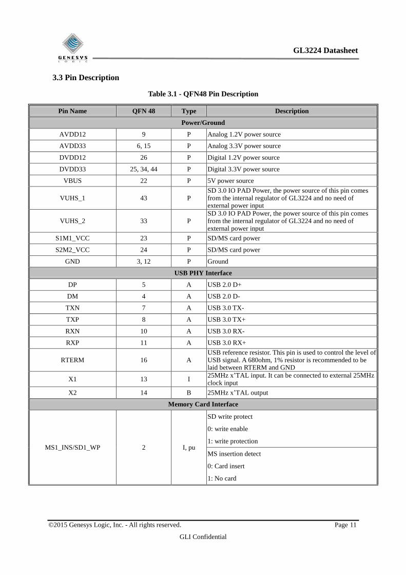
3.3 Pin Description
Table 3.1 - QFN48 Pin Description
Pin Name QFN 48 Type Description
Power/Ground
AVDD12 9 P Analog 1.2V power source
AVDD33 6, 15 P Analog 3.3V power source
DVDD12 26 P Digital 1.2V power source
DVDD33 25, 34, 44 P Digital 3.3V power source
VBUS 22 P 5V power source
VUHS_1 43 P SD 3.0 IO PAD Power, the power source of this pin comes from the internal regulator of GL3224 and no need of external power input
VUHS_2 33 P SD 3.0 IO PAD Power, the power source of this pin comes from the internal regulator of GL3224 and no need of external power input
S1M1_VCC 23 P SD/MS card power
S2M2_VCC 24 P SD/MS card power
GND 3, 12 P Ground
USB PHY Interface
DP 5 A USB 2.0 D+
DM 4 A USB 2.0 D-
TXN 7 A USB 3.0 TX-
TXP 8 A USB 3.0 TX+
RXN 10 A USB 3.0 RX-
RXP 11 A USB 3.0 RX+
RTERM 16 A USB reference resistor. This pin is used to control the level of USB signal. A 680ohm, 1% resistor is recommended to be laid between RTERM and GND
X1 13 I 25MHz x’TAL input. It can be connected to external 25MHz clock input
X2 14 B 25MHz x’TAL output
Memory Card Interface
MS1_INS/SD1_WP 2 I, pu
SD write protect
0: write enable
1: write protection
MS insertion detect
0: Card insert
1: No card
GL3224 Datasheet
© 2015 Genesys Logic, Inc. - All rights reserved. Page 12
GLI Confidential
MS2_INS/SD2_WP 35 I, pu
SD write protect
0: write enable
1: write protection
MS insertion detect
0: Card insert
1: No card
SD1_CDZ 1 I, pu
SD card detect
0: Card insert
1: No card
SD2_CDZ 36 I, pu
SD card detect
0: Card insert
1: No card
S2D1_M2BS 27 B SD data pin
O MS/MSP bus state
S2D0_M2D1 28 B SD data pin
B MS/MSP data signal
S2CK_M2D0 29
O SD clock
B MS/MSP data signal
S2CM_M2D2 30
B,pu SD command/response
B MS/MSP data signal
S2D3_M2D3 31
B SD data pin
B MS/MSP data signal
S2D2_M2CK 32
B SD data pin
O MS clock
S1D1_M1BS
37
B SD data pin
O MS/MSP bus state
S1D0_M1D1 38 B SD data pin
B MS/MSP data signal
S1CK_M1D0 39 O SD clock
B MS/MSP data signal
S1CM_M1D2 40 B,pu SD command/response

GL3224 Datasheet
© 2015 Genesys Logic, Inc. - All rights reserved. Page 13
GLI Confidential
B MS/MSP data signal
S1D3_M1D3 41 B SD data pin
B MS/MSP data signal
S1D2_M1CK 42 B SD data pin
O MS clock
S1D7_M1D4 45 B SD data pin
B MS/MSP data signal
S1D6_M1D5 46 B SD data pin
B MS/MSP data signal
S1D5_M1D6 47 B SD data pin
B MS/MSP data signal
S1D4_M1D7 48 B SD data pin
B MS/MSP data signal
Others
LED 21 O Memory card access LED
SPI_CS 20 O SPI interface: chip select
SPI_CK 19 O SPI interface: clock
SPI_MISO 17 I SPI interface: connect to SPI flash data output
SPI_MOSI 18 O SPI interface: connect to SPI flash data input
Notation:
Type O Output
I Input
B Bi-directional
pu internal pull-up when input
pd internal pull-down when input
P Power / Ground
A Analog
GL3224 Datasheet
© 2015 Genesys Logic, Inc. - All rights reserved. Page 14
GLI Confidential
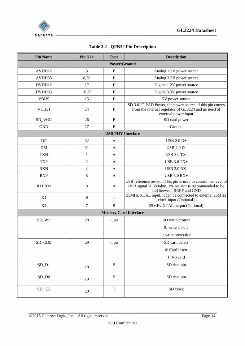
Table 3.2 - QFN32 Pin Description
Pin Name Pin NO. Type Description
Power/Ground
AVDD12 3 P Analog 1.2V power source
AVDD33 8,30 P Analog 3.3V power source
DVDD12 17 P Digital 1.2V power source
DVDD33 16,25 P Digital 3.3V power source
VBUS 15 P 5V power source
VUHSI 24 P SD 3.0 IO PAD Power, the power source of this pin comes
from the internal regulator of GL3224 and no need of external power input
SD_VCC 26 P SD card power
GND 27 P Ground
USB PHY Interface
DP 32 A USB 2.0 D+
DM 31 A USB 2.0 D-
TXN 1 A USB 3.0 TX-
TXP 2 A USB 3.0 TX+
RXN 4 A USB 3.0 RX-
RXP 5 A USB 3.0 RX+
RTERM 9 A USB reference resistor. This pin is used to control the level of
USB signal. A 680ohm, 1% resistor is recommended to be laid between RREF and GND
X1 6 I 25MHz XTAL input. It can be connected to external 25MHz
clock input (Optional)
X2 7 B 25MHz XTAL output (Optional)
Memory Card Interface
SD_WP 28 I, pu SD write protect
0: write enable
1: write protection
SD_CDZ 29 I, pu SD card detect
0: Card insert
1: No card
SD_D1
18
B SD data pin
SD_D0
19
B SD data pin
SD_CK
20
O SD clock

GL3224 Datasheet
© 2015 Genesys Logic, Inc. - All rights reserved. Page 15
GLI Confidential
SD_CM
21
B,pu SD command/response
SD_D3
22
B SD data pin
SD_D2
23
B SD data pin
Others
LED 14 O Memory card access LED
SPI_CS 13 O SPI interface: chip select
SPI_CK 12 O SPI interface: clock
SPI_MISO 10 I SPI interface: Connect to SPI flash data output
SPI_MOSI 11 O SPI interface: Connect to SPI flash data input
Notation:
Type O Output
I Input
B Bi-directional
pu internal pull-up when input
pd internal pull-down when input
P Power / Ground
A Analog

GL3224 Datasheet
© 2015 Genesys Logic, Inc. - All rights reserved. Page 16
GLI Confidential
CHAPTER 4 BLOCK DIAGRAM
xHCI
EHCI
EP0 FIFO
BULK FIFO
EPFIFO
8051
CORE
Control
Register
RAM
MCU
MHE
3.3V to 1.2V
Regulator
5V to 3.3V
ROM
USB
Controller HS/FS
PHY
SuperSpeed
PHY
SD3.0/MMC
8-bit I/F
MS-PRO/HG
8-bit I/F
PLL
SPI
Flash
microSD3.0/M2
4-bit I/F
Figure 4.1 – QFN48 Functional Block Diagram
xHCI
EHCI
EP0 FIFO
BULK FIFO
EPFIFO
8051
CORE
Control
Register
RAM
MCU
MHE
3.3V to 1.2V
Regulator
5V to 3.3V
ROM
USB
Controller HS/FS
PHY
SuperSpeed
PHY
SD3.0/MMC
8-bit I/F
PLL
SPI
Flash
Figure 4.2 – QFN32 Functional Block Diagram
GL3224 Datasheet
© 2015 Genesys Logic, Inc. - All rights reserved. Page 17
GLI Confidential
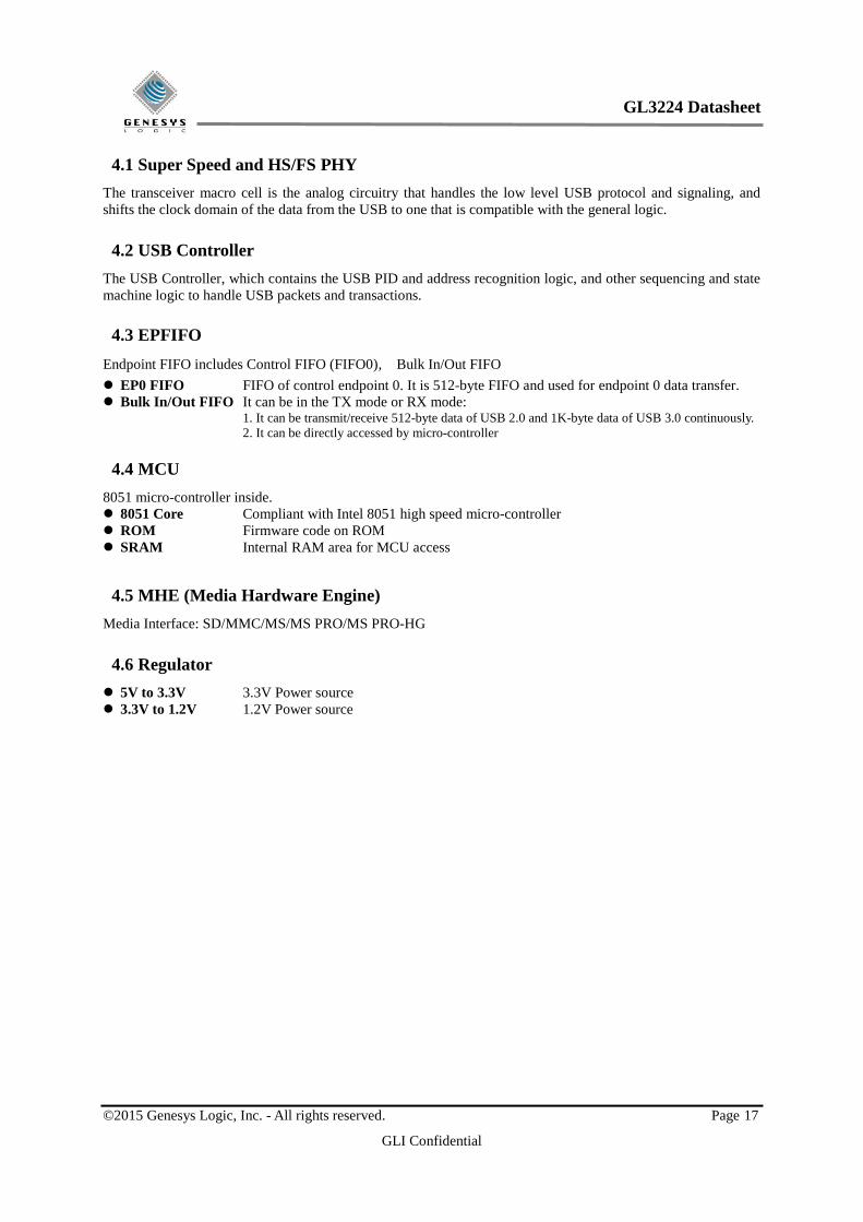
4.1 Super Speed and HS/FS PHY
The transceiver macro cell is the analog circuitry that handles the low level USB protocol and signaling, and
shifts the clock domain of the data from the USB to one that is compatible with the general logic.
4.2 USB Controller
The USB Controller, which contains the USB PID and address recognition logic, and other sequencing and state
machine logic to handle USB packets and transactions.
4.3 EPFIFO
Endpoint FIFO includes Control FIFO (FIFO0), Bulk In/Out FIFO
EP0 FIFO FIFO of control endpoint 0. It is 512-byte FIFO and used for endpoint 0 data transfer.
Bulk In/Out FIFO It can be in the TX mode or RX mode: 1. It can be transmit/receive 512-byte data of USB 2.0 and 1K-byte data of USB 3.0 continuously.
2. It can be directly accessed by micro-controller
4.4 MCU
8051 micro-controller inside.
8051 Core Compliant with Intel 8051 high speed micro-controller
ROM Firmware code on ROM
SRAM Internal RAM area for MCU access
4.5 MHE (Media Hardware Engine)
Media Interface: SD/MMC/MS/MS PRO/MS PRO-HG
4.6 Regulator
5V to 3.3V 3.3V Power source 3.3V to 1.2V 1.2V Power source
GL3224 Datasheet
© 2015 Genesys Logic, Inc. - All rights reserved. Page 18
GLI Confidential
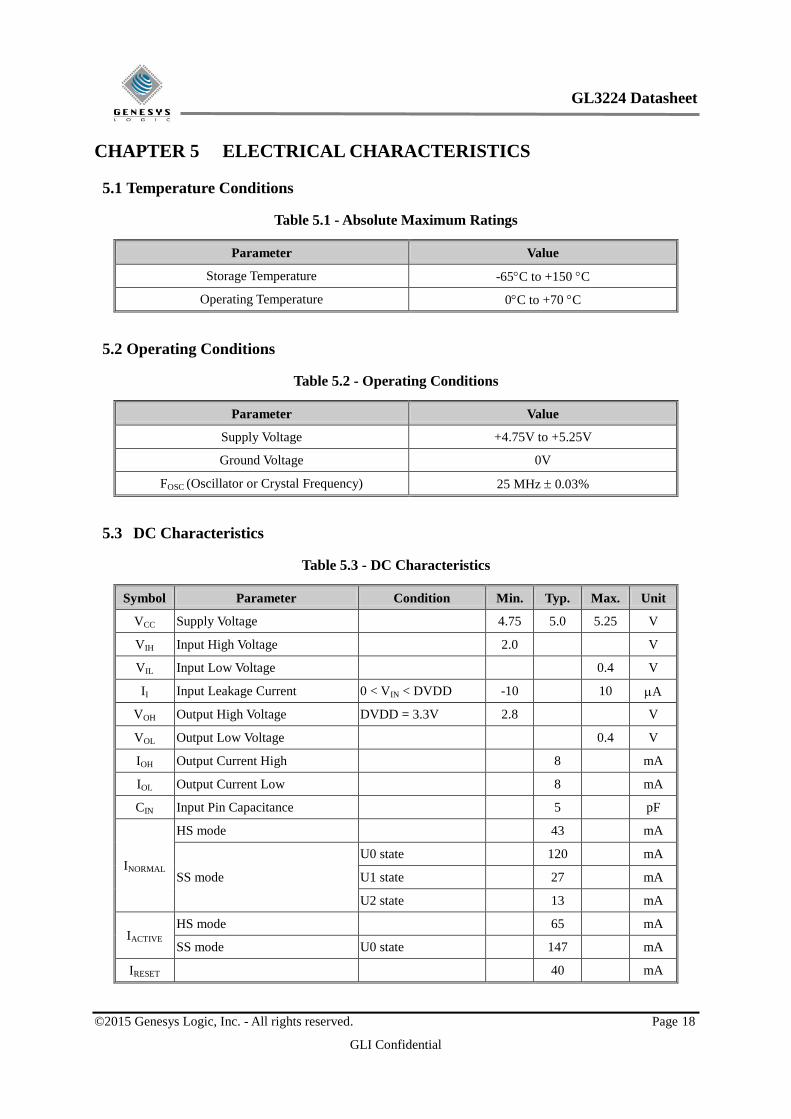
CHAPTER 5 ELECTRICAL CHARACTERISTICS
5.1 Temperature Conditions
Table 5.1 - Absolute Maximum Ratings
Parameter Value
Storage Temperature -65C to +150 C
Operating Temperature 0C to +70 C
5.2 Operating Conditions
Table 5.2 - Operating Conditions
Parameter Value
Supply Voltage +4.75V to +5.25V
Ground Voltage 0V
FOSC (Oscillator or Crystal Frequency) 25 MHz 0.03%
5.3 DC Characteristics
Table 5.3 - DC Characteristics
Symbol Parameter Condition Min. Typ. Max. Unit
VCC Supply Voltage 4.75 5.0 5.25 V
VIH Input High Voltage 2.0 V
VIL Input Low Voltage 0.4 V
II Input Leakage Current 0 < VIN < DVDD -10 10 A
VOH Output High Voltage DVDD = 3.3V 2.8 V
VOL Output Low Voltage 0.4 V
IOH Output Current High 8 mA
IOL Output Current Low 8 mA
CIN Input Pin Capacitance 5 pF
INORMAL
HS mode 43 mA
SS mode
U0 state 120 mA
U1 state 27 mA
U2 state 13 mA
IACTIVE HS mode 65 mA
SS mode U0 state 147 mA
IRESET 40 mA

GL3224 Datasheet
© 2015 Genesys Logic, Inc. - All rights reserved. Page 19
GLI Confidential
ISUS Suspend current 1.5K pull-up included 0.85 mA
SS Suspend current U3 state 0.7 mA
Rpu
Reset Pad pull-up 46 KΩ
SD_CDZ, SD_WP, MS_INS,
GPIO Pad pull-up
46 KΩ
SD_CMD pull-up 15 KΩ
SD_CLK, D[3:0] Pad pull-up 15 KΩ
Rpd SD_CMD pull-down 15 KΩ
SD_CLK, D[3:0] Pad pull-down 15 KΩ
RIMP SD_CMD, SD_CLK, D[3:0]
impedances
50 Ω
5.4 AC Characteristics of Reset Timing
5.4.1 Reset Timing
RSTZ
TRST
Figure 5.1 - Timing Diagram of Reset Width

GL3224 Datasheet
© 2015 Genesys Logic, Inc. - All rights reserved. Page 20
GLI Confidential
AVDD
3V
USB2.0
Command
RSTZ
T1
T2
2V
Clock
SuperSpeed
Termination
T3
Termination ON
Figure 5.2 - Timing Diagram of Power Good to USB Command Receive Ready
Table 5.4 - Reset Timing
Parameter Description Min. Unit
TRST Chip reset sense timing width 2 us
T1 AVDD power up to reset de-assert 500 us
T2 Reset de-assert to respond USB command ready 95 ms
T3 Reset de-assert to SuperSpeed termination on 12 ms
5.4.2 SD/MMC Card Clock Frequency
Table 5.5 - SD/MMC Card Clock Frequency
Parameter Description Max. Unit
FID Clock frequency Identification Mode 400 KHz
FDS Clock frequency Default Speed Mode 25 MHz
FHS SD Clock frequency High Speed Mode 50 MHz
FHS MMC Clock frequency High Speed Mode 52 MHz
FSDR25 Clock frequency Ultra High Speed Mode: SDR25 50 MHz

GL3224 Datasheet
© 2015 Genesys Logic, Inc. - All rights reserved. Page 21
GLI Confidential
FDDR50 Clock frequency Ultra High Speed Mode: DDR50 50 MHz
FSDR50 Clock frequency Ultra High Speed Mode: SDR50 100 MHz
FSDR104 Clock frequency Ultra High Speed Mode: SDR104 208 MHz
5.4.3 e•MMC Clock Frequency
Table 5.6 - e•MMC Clock Frequency
Parameter Description Max. Unit
FID Clock frequency Identification Mode 400 KHz
FSDR Clock frequency High Speed SDR 52 MHz
FDDR Clock frequency High Speed DDR 52 MHz
FHS200 Clock frequency HS200 200 MHz
5.4.4 MS Card Clock Frequency
Table 5.7 - MS Card Clock Frequency
Parameter Description Max. Unit
FDS Clock frequency Default Speed Mode 20 MHz
FMSP Clock frequency MS PRO 4bit Mode 40 MHz
FMSPHG Clock frequency MS PRO HG 8bit Mode 60 MHz

GL3224 Datasheet
© 2015 Genesys Logic, Inc. - All rights reserved. Page 22
GLI Confidential
CHAPTER 6 SPI FLASH MEMORY SUPPORT LIST
Table 6.1 - SPI Flash Memory Support List
Vendor Model
GigaDevice
GD25Q512
GD25Q010
GD25Q040
PMC
PM25LD512C
PM25LD010
PM25LD010C
PM25LD020
PM25LD020C
WINBON
W25X05CL
W25X10CL
W25X10BV
W25X20CL
W25X20BV
EON EN25Q40
MXIC MX25L1006E
ESMT F25L01PA-86PG
F25L01PA-100PG
Giantec GT25F512
Note :
- GL3224 support Page-Program SPI Flash Memory only, does not support Byte-program SPI Flash Memory
- The density of SPI Flash Memory shall be larger than or equal to 512Kbit.
- Firmware file (xxxx.bin) which Genesys Logic provided is only used for Genesys Logic’s Multi-Tool and MP
Tool ISP (In System Programming via USB interface) purpose. If you would like to provide FW to SPI Flash
vendor for pre-loading or Flash ROM writer usage, please contact to GL technical support team.

GL3224 Datasheet
© 2015 Genesys Logic, Inc. - All rights reserved. Page 23
GLI Confidential
CHAPTER 7 PACKAGE DIMENSION
Figure 7.1 - QFN 48 Pin Package

GL3224 Datasheet
© 2015 Genesys Logic, Inc. - All rights reserved. Page 24
GLI Confidential
Figure 7.2 - QFN 32 Pin Package
GL3224 Datasheet
© 2015 Genesys Logic, Inc. - All rights reserved. Page 25
GLI Confidential
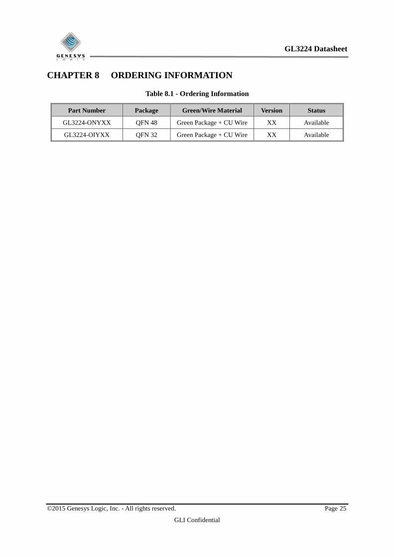
CHAPTER 8 ORDERING INFORMATION
Table 8.1 - Ordering Information
Part Number Package Green/Wire Material Version Status
GL3224-ONYXX QFN 48 Green Package + CU Wire XX Available
GL3224-OIYXX QFN 32 Green Package + CU Wire XX Available