Embed Size (px)
Citation preview

MATILDA: A MASS FILTERED NANOCLUSTER SOURCE
by
GIHAN KWON
A DISSERTATION
Submitted in partial fulfillment of the requirements for the degree of Doctor of Philosophy in the
Department of Chemical and Biological Engineering in the Graduate School of
The University of Alabama
TUSCALOOSA, ALABAMA
2009

Copyright GiHan Kwon 2009 ALL RIGHTS RESERVED
ii
Submitted by GiHan Kwon in partial fulfillment of the requirements for the
degree of Doctor of Philosophy specializing in Chemical and Biological Engineering.
Accepted on behalf of the Faculty of the Graduate School by the dissertation
committee:
Alan M. Lane, Ph.D
C. Heath. Turner, Ph.D.
Mark L. Weaver, Ph.D.
Gary J. Mankey, Ph.D.
Tonya M. Klein, Ph.D. Chairperson
Viola L. Acoff, Ph.D. Department Chairperson
Date
David A. Francko, Ph.D. Dean of the Graduate School
Date

iii
LIST OF ABBREVIATIONS AND SYMBOLS
BTU British thermal unit
DOE Department of Energy
PEMFC Polymer electrolyte membrane fuel cells
FT-IR Fourier transform infrared spectroscopy
UHV Ultra high vacuum
STM Scanning tunneling microscopy
DC Direct current
RF Radio frequency
PACIS Pulsed arc cluster source
QMF Quadrupole mass filter
WVF Wien velocity filter
MSMF Magnetic sector mass filter
TOF Time-of-flight
amu Atomic mass unit
PFMS Pulsed field mass selector
V(t) Total potential
VDC Direct potential
VRF Amplitude of radio frequency voltage
M Ion mass
ΔM Difference in mass between two resolvable peaks in a mass spectrum

iv
R Mass resolution
XPS X-ray photoelectron spectroscopy
AFM Atomic force microscopy
TEM Transmission electron microscopy
CCD Charged coupled device camera
STEM Scanning transmission electron microscopy
EDX Energy dispersive X-ray spectroscopy
EELS Electron energy loss spectroscopy
ADF Annular dark field
HAADF High angle annular dark field
B. E Binding energy
RFA Retarding Field Analyzer
MFC Mass flow controller
CEM Channeltron electron multiplier
OD Outside diameter
L/s Litter per second
eV Electron volt
FWHM Full width at half maximum

v
ACKNOWLEDGMENTS
I would like to thank my advisors, Tonya Klein and Gary Mankey, for their
consistent guidance, support, and encouragement in my research. I would like to thank
my dissertation committee members, Alan Lane, Mark Weaver, and Heath Turner, for
their valuable suggestions. I would like to thank my lab members, Harish Bhandari, Ping
Chen, Lucas Falco, Shilpa Dubey, Jinwen Wang, Ning Li, and Kejing Li for their helping,
kindness, and sharing. I am thankful for the opportunity to work with the nanocatalyst
research team: John Wiest, Shane Street, David Nikles, Zhufang Liu, Wei Li, James
Burgess, Chethan Acharya, and Brian Flowers. I would like to thank the faculty, staff,
and graduate students of the Department of Chemical and Biological Engineering at the
University of Alabama for their support. I would like to express my appreciation for
financial support from Department of Chemical and Biological Engineering and also
from DOE EPSCoR, Alabama EPSCoR, NSF equipment sharing, Central Analytical
Facility, and KOSEF (Korea Science and Engineering Foundation). I really appreciate
AJA international, Inc., the physics machine shop: David Key, Joe Howell, and Michael
Perrigin; and the Physics electronic shop: Danny Whitcomb and Jason Kuykendall for
their consistent supports.
I would like to thank my parents and my family for their encouragement and
spiritual support.
Now faith is being sure of what we hope for and certain of what we do not see. This is
what the ancients were commended for. -Hebrews11:1-2

vi
CONTENTS LIST OF ABBREVIATIONS AND SYMBOLS .............................................................. iii
ACKNOWLEDGMENTS .................................................................................................. v
LIST OF FIGURES ............................................................................................................ x
ABSTRACT..................................................................................................................... xiv
CHAPTER I. INTRODUCTION....................................................................................... 1
Motivation............................................................................................................... 1
Preparations of Metal Catalysts .............................................................................. 2
Impregnation Techniques............................................................................ 3
Colloid Chemistry Technique ..................................................................... 3
Lithography Technique............................................................................... 4
Vacuum Technique ..................................................................................... 6
CHAPTER II. CLUSTER BEAM TECHNOLOGY......................................................... 8
Cluster Source......................................................................................................... 8
Gas Condensation Cluster Source............................................................... 9
Laser Ablation Cluster Source .................................................................. 10
Sputtering Cluster Source ......................................................................... 11
Pulsed Arc Cluster Ion Source.................................................................. 13
Mass Filter ............................................................................................................ 13
Quadrupole Mass Filter (QMF) ................................................................ 14
Wien Velocity Filter (WVF)..................................................................... 16
vii
Time of Flight (TOF)................................................................................ 17
Pulsed Field Mass Selector (PFMS) ......................................................... 18
Magnetic Sector Mass Filter (MSMF)...................................................... 18
CHAPTER III. CHARACTERIZATION TECHNIQUES.............................................. 20
X-Ray Photoelectron Spectroscopy (XPS) ........................................................... 20
Atomic Force Microscopy (AFM)........................................................................ 21
Transmission Electron Microscopy (TEM) .......................................................... 23
CHAPTER IV. EXPERIMENTAL SETUP .................................................................... 25
Matilda: Nanocluster System................................................................................ 26
Retarding Field Analyzer...................................................................................... 32
Three-Element Lenses .......................................................................................... 34
Magnetic Sector Mass Filter for Mass Separation................................................ 36
Detection Methods of Charged Particle................................................................ 38
Modification of Nanocluster Source..................................................................... 41
CHAPTER V. PERFORMANCE OF MATILDA .......................................................... 43
Pressure Ratio of Helium to Argon....................................................................... 43
Ion Energy Distribution ........................................................................................ 49
Ion Optics for Retarding Field Analyzer .............................................................. 54
CHAPTER VI. PROGRESS OF SIZE SELECTION OF CLUSTER............................. 60
Beam Profile ......................................................................................................... 60
Magnetic Field Distribution in Magnetic Sector Mass Filter ............................... 63
Size Selection of Cluster....................................................................................... 64
2nd Version of Lens for Focusing Beam ............................................................... 69

viii
CHAPTER VII. CONCLUSION AND FUTURE WORK.............................................. 72
Conclusions........................................................................................................... 72
Future Work.......................................................................................................... 74
REFERENCES ................................................................................................................. 76
APPENDIX A. SCHEMATICS OF NANOCLUSTER SOURCES............................... 84
APPENDIX B. PERFORMANCE OF 1ST VERSION OF NANOCLUSTER SOURCE................................................................................................ 86
AFM Images (Scale: 1×1μm) ............................................................................... 86
Experimental Conditions ...................................................................................... 88
Particle Size Distribution ...................................................................................... 88
TEM Images.......................................................................................................... 89
Experimental Conditions ...................................................................................... 90
Particle Size Distribution ...................................................................................... 91
APPENDIX C. ION ENERGY DISTRIBUTION OF 1ST VERSION RFA ................... 92
APPENDIX D. SCHEMATIC OF APERTURE............................................................. 94
APPENDIX E. LABVIEW PROGRAMMING ............................................................... 95
Depositter of Nanoclusters.................................................................................... 95
Analyzer for Measuring Ion Energy Distribution................................................. 96
Detector for Measuring Ion Voltage Signal from CEM ....................................... 96
APPENDIX F. SIMULATION CODING FOR RFA AND LENS................................. 97
APPENDIX G. SIMULATION CODING FOR MSMF............................................... 102
APPENDIX H. MAXIMUM CLUSTER LANDING ENERGY.................................. 103

ix
APPENDIX I. SCHEMATIC DIAGRAM OF 2nd VERSION OF LENS AND LENS HOLDER ............................................................................................. 104
Schematic Diagram of 2nd Version of Lens ........................................................ 104
Lens Holder......................................................................................................... 105

x
LIST OF FIGURES
1. Schematic diagram of a typical gas condensation cluster source .................................. 9
2. A laser ablation cluster source ..................................................................................... 10
3. Sputtering cluster source : (a) using an ion gun to accelerate ions to the target and (b) using a magnetron-based plasma as an ion source for sputtering............................... 12
4. Mass filters for charged clusters: (a) RF quadrupole, (b) wien velocity, (c) TOF mass
spectrometer with direct and reflection, and (d) pulsed filed mass selector. Δt is time delay between the end of acceleration pulse and the start of the deceleration pulse. Up is the voltage pulse height........................................................................................... 16
5. (a) Basic principle of the motion of an ions in a magnetic field. (b) The effect of a
magnetic field on the ion trajectory. B is the magnetic field. F is the force on an ion in a homogeneous magnetic field. v is ion velocity ........................................................ 19
6. (a) The basic principle of X-ray photoelectron spectroscopy and (b) concentric
hemispherical analyzer used in XPS........................................................................... 21 7. Schematic diagram of the AFM system in tapping mode............................................ 22
8. Schematic diagrams of (a) TEM and (b) STEM.......................................................... 24 9. Schematic of the sections making up the complete size-selected nanocluster source
system ......................................................................................................................... 26 10. Schematic of the control system mounted on (a) sample holder/CEM, (b) accessory
port including mass spectrometer, CEM holder, view port, and three electrical feedthroughs, (c) RFA, (d) sputter gun with target (red), (e) water in and out line, (f) electrical feedthrough port, (g) electrical lines for RFA grids, (h) pumping port for evacuating contaminant in aggregation tube, (i) convection gauge to measure pressure of aggregation tube, (j) gas mixture inlet line, (k) clamp for adjusting aggregation distance, and (l) electrical housing............................................................................. 28

xi
11. Schematic of gas line: (a) 0 ~ +5 VDC for flow signal output, (b) 0 ~ 10 KΩ Heliport 10 turn potentiometer for controlling flow signal output voltage, (c) mass flow controller, (d) gas mixture line to introduce into aggregation tube, (e) Ar inlet line, (f) He inlet line, and (g) ±15 VDC power for mass flow controller. SCB-68 is a shielded I/O connector block for data communication between DAQ card and computer from National Instruments................................................................................................... 29
12. Comparison with (a) Harberland type, (b) conventional type of magnetron sputter gun
..................................................................................................................................... 30
13. Schematic of the basic principle of retarding field analyzer....................................... 33
14. (a) 1st version and (b) 2nd version of RFA, and their grids shown as insets. The holes on cover of (b) vent the gas mixture to prevent a short circuit at high voltage……...34
15. SIMION simulation of an Einzel lens. (a) cross sectional view of an Einzel lens with
electric potential line (red line). Two electrodes are set to ground potential, the middle electrode to +110V. (b) three-dimensional view of the three electrodes and the particle beam. (c) and (d) show focusing effect in a different electric field of middle electrode. Roll outward shows positive and roll inward indicates negative potential.35
16. Picture of the three-element lenses used for Matilda.................................................. 36 17. Schematic of MSMF for mass separation................................................................... 37
18. Picture of MSMF: (a) cover, (b) neodymium block, (c) pink colored insulator, (d)
supporter with bolt and nut, and (e) electrical connector............................................ 38
19. Schematics of (a) Faraday cup and (b) CEM for detection of negatively charged ions.............................................................................................................................. 39
20. The circuit of CEM with discriminator (AMPTEK A101 and PC-10 board)............. 40
21. The pictures of the modification of the 1st version cluster source. (a) Deposited place
after deposition, (b) pumping port and feedthrough for RFA, and electrical line with (c) 1st and (d) 2nd versions of the RFA........................................................................ 42
22. (a) HAADF image, (b) EDX analysis of Ag on c-TEM grid in red circle area of (a),
and (c) XPS spectra of Ag/Si. Red lines are for Ag and black lines are for substrate ...................................................................................................................... 45
23. TEM images of Ag on c-coated grid with RFA as pressure ratio of He to Ar (a) 0, (b)
2.5 (c) 4.5, (d) 6, and (e) 9.5 at 2˝ aggregation distance and 20 minutes deposition.................................................................................................................... 46
24. Particle size distribution from Fig. 23......................................................................... 47

xii
25. Saturation ion current vs. pressure ratio (He/Ar) at 20 watt sputter power (Pressure ratio = 0 (only 0.4 sccm of Ar)) .................................................................................. 48
26. Ion energy distribution with different sputter power at 2˝ aggregation distance and 0.4
sccm Ar flow rate (solid line is the indicator of the center of ion energy distribution)..................................................................................................................................... 50
27. Ion energy distribution with different aggregation distances at 20 watt sputter power
and a 0.4sccm Ar flow rate ......................................................................................... 51
28. Ion energy distribution with different He flow rates at 0.4 sccm Ar with 20watt sputter power and 2˝ aggregation distance ................................................................. 52
29. Ion energy distribution with different acceleration voltages at a zero pressure ratio
and at 0.4 sccm Ar with 20 watt sputter power and 2˝ aggregation distance. G1and G2 are applied with an acceleration voltage and G3 is the retarding grid........................ 53
30. Maximum cluster landing energy at different pressure ratios (He/Ar)....................... 54
31. (a) Five grids and ceramic spacer in retarding field analyzer with magnification of
100% transparency copper mesh (real grids have 80% transparence) of each grid. (b) Beam trajectories for retarding voltage (-5V) at G2 (200V). Initial K.E of black and red line = 5eV and other lines have 6eV. (c) Beam trajectories for retarding voltage (-9V) at G2 (200V). Initial K.E of black and red line = 9eV and other lines have 10eV. Sample holder is grounded.......................................................................................... 56
32. (a) Ion current and (b) number of particles collected from TEM images................... 57
33. TEM image and particle size distribution at -5V of retarding voltage with a 6.0
pressure ratio at G1 = +200V. Other grids and sample holder are grounded ............. 58 34. TEM image and particle size distribution at -9V of retarding voltage with a 9.5
pressure ratio at G1 = +200V. Other grids and sample holder are grounded ............. 59 35. RFA and three-element lenses in SIMION for the potential setting. G0: ground, G1 ~
C: +20V, V1 and V3: +20V, and V2: +100V. This condition makes the beam spread the least after passing the lens..................................................................................... 61
36. (a) The distribution of ions from the simulation and (b) simulated and experiment at
0.15˝ from lens. The ion beam is approximately 0.2˝ in diameter. Blue line in (a) is the beam profile line for (b). Deflector can shift the experimental peak to the simulation result.......................................................................................................... 61
37. The ion beam profile of 1.4˝ distance from MSMF. Beam diameter is 0.7˝ .............. 62

xiii
38. The real area for size selection after MSMF. Beam diameter is 0.5˝ and 0.7˝ from direct behind and 1.4˝ from MSMF. Yellow color is magnet and gray color is the cover of magnets. CEM must be installed as close as possible to increase selection region. Six TEM grids (from 0 to 5 in red circle) were installed at the end of MSMF at intervals of 0.5˝. TEM grid (0 in red circle) is neutral position ............................. 63
39. Comparison between (a) real magnetic field and (b) simulated magnetic field. Red
line is the size of magnet. Both show the magnetic field without magnets ................ 64 40. Ion trajectories of (a) 50eV kinetic energy for low mass (≥ 2.0nm), (b) 4eV for the
zero pressure ratio, and (c) 1eV kinetic energy for high mass (≤ 2.0nm)................... 65 41. CEM data of Ag clusters at different positions........................................................... 66 42. CEM spectrum of negatively charged Ag nanoparticles. 0 position of CEM is for
neutral and large clusters. All signals of positions are averaged and normalized from the previous figure ...................................................................................................... 67
43. Ag clusters on the TEM grids at the neutral position ................................................. 68 44. Ag clusters on the TEM grids at the 0.5˝ position...................................................... 69 45. 2nd version of three-element lens. a is the holder for installation on the cluster source.
b is the electrical connector. c is the holder for fixing three tubes (V1, V2, and V3). d is the ceramic rod from electric field. e is the hole for threaded rods which are connected with cluster source. g is the beam guider................................................... 70
46. (a) 2nd version of Einzel lens to minimize the beam spread including g, beam guider.
(b) Beam trajectory at V1 and V3 = +20V, V2 = +100V. (c) Beam trajectory at V1 and V3 = +1.0kV, and V3 = +2.0kV .......................................................................... 71
47. Ion energy distribution at 4˝aggregation distance ...................................................... 92 48. Ion energy distribution at 6˝aggregation distance ...................................................... 93 49. Ion energy distribution at 8˝aggregation distance ...................................................... 93

xiv
ABSTRACT
Cluster science provides a good model system for the study of the size
dependence of electronic properties, chemical reactivity, as well as magnetic properties
of materials. One of the main interests in cluster science is the nanoscale understanding
of chemical reactions and selectivity in catalysis. Therefore, a new cluster system was
constructed to study catalysts for applications in renewable energy. Matilda, a
nanocluster source, consists of a cluster source and a Retarding Field Analyzer (RFA). A
moveable AJA A310 Series 1″-diameter magnetron sputtering gun enclosed in a water
cooled aggregation tube served as the cluster source. A silver coin was used for the
sputtering target. The sputtering pressure in the aggregation tube was controlled, ranging
from 0.07 to 1torr, using a mass flow controller. The mean cluster size was found to be a
function of relative partial pressure (He/Ar), sputtering power, and aggregation length.
The kinetic energy distribution of ionized clusters was measured with the RFA. The
maximum ion energy distribution was 2.9 eV/atom at a zero pressure ratio. At high Ar
flow rates, the mean cluster size was 20 ~ 80nm, and at a 9.5 partial pressure ratio, the
mean cluster size was reduced to 1.6nm. Our results showed that the He gas pressure can
be optimized to reduce the cluster size variations. Results from SIMION, which is an
electron optics simulation package, supported the basic function of an RFA, a three-
element lens and the magnetic sector mass filter. These simulated results agreed with
experimental data. For the size selection experiment, the channeltron electron multiplier
collected ionized cluster signal at different positions during Ag deposition on a TEM grid

xv
for four and half hours. The cluster signal was high at the position for neutral clusters,
which was not bent by a magnetic field, and the signal decreased rapidly far away from
the neutral cluster region. For cluster separation according to mass to charge ratio in a
magnetic sector mass filter, the ion energy of the cluster and its distribution must be
precisely controlled by acceleration or deceleration. To verify the size separation, a high
resolution microscope was required. Matilda provided narrow particle sized distribution
from atomic scale to 4nm in size with different pressure ratio without additional mass
filter. It is very economical way to produce relatively narrow particle size distribution.

1
CHAPTER I
INTRODUCTION
Motivation
Fuel cell technology holds the promise of revolutionizing energy conversion in
that it can provide an efficient and clean alternative to fossil fuel. Currently, fuel cells are
used to provide power in stationary and portable power applications in remote locations
or as emergency backup. However, future applications may include the replacement of
the gasoline engine or integration of fuel cells as an integral part of a hybrid vehicle as
well as to power portable electronic devices such as laptops and cell phones. A fuel cell
generates electricity by a chemical reaction occurring at two electrodes separated by an
electrolyte through which electrically-charged particles travel from one electrode to the
other. A catalyst on the electrodes facilitates the reaction. Hydrogen is a basic fuel;
however, other fuels such as methanol can be more convenient in that a liquid fuel is
easier to store and transport and has a larger BTU/volume ratio. In either case, the
hydrogen and oxygen used in generating electricity ultimately combine to form water as a
harmless by-product, as well as CO2 in carbon containing fuels.
The Department of Energy (DOE) Office of Efficiency and Renewable Energy's
Hydrogen, Fuel Cells & Infrastructure Technologies Program has identified cost and
durability as two of the main barriers to the commercialization of polymer electrolyte
membrane fuel cells (PEMFC).1 A major factor in cost is the catalyst material, which

2
contains precious metal such as platinum.2 To minimize the amount of catalyst needed, a
high surface to volume ratio of the catalyst particles is desirable to maximize the surface
area available for the reaction. Proper dispersion of particle size enables low-load catalyst
design for an overall lower system cost. In addition, particles must maintain their
structure over the lifetime of the fuel cell, as a change in the morphology from the initial
state would result in a loss of electrochemical activity. Agglomeration of particles due to
diffusion and sintering is considered to be a major cause for the decrease in fuel cell
performance, and this problem increases for smaller catalyst size distributions.3
As a model system, in order to understand the effect of the substrate-particle
interaction as a function of nanoparticle size as well as the modification of the support, a
nanocluster source (Matilda) was developed for the deposition of size-selected
nanoparticles in a range from atomic scale to 10nm. The research team planned to
develop Matilda (a mass filtered nanocluster source) to produce size-selected
nanoparticles for further application of the observation of diffusion and sintering
behavior using sophisticated surface analysis.
Preparation of Metal Catalysts
Several methods have been developed to load metal particles on high surface area
support materials.4, 5 Catalysts nanoparticles are deposited on a high surface area porous
support so that large surface areas of the metal particles are catalytically active. This
section has brief reviews of the most common methods for preparing a supported model
catalyst, including their advantages and limitations.

3
Impregnation Technique
The standard method to produce catalysts is impregnation, a commonly used
technique for the synthesis of heterogeneous catalysts, in which the porous oxide support
is impregnated with metal precursors (e.g., H2PtCl6 for Pt and PdCl2 for Pd) in a solution
phase, followed by thermal treatment and/or reduction with H2 to form metal
nanoparticles.6 Typically, the active metal precursor is dissolved in an aqueous or organic
solution. Then, the metal-containing solution is added to a catalyst support with the same
pore volume as the volume of solution that was added. Capillary action introduces the
solution into the pores of support. The catalyst can then be dried and calcined to remove
undesired and volatile components within the solution, to activate the catalyst, and to
load the metal on the catalyst surface.6 This method is good for the large scale production
of catalysts,7 and the particle size distribution produced on the support is nonuniform in
size, shape, and metal-support interaction as well as structure.6, 8 On the other hand,
stable catalysts at operating temperatures are produced with a high particle density.6
Colloid Chemistry Technique
Colloid chemistry is one of the main techniques for the synthesis of size
controlled nanoparticles of metal, semiconductor, and magnetic materials. Synthesis of
particles using this technique has several advantages. The colloidal technique can not
only precisely control the particle size up to 30nm, but also shape, to some extent. In
addition, it has high throughput and enlarges the surface area of particle-loaded 3D
support surfaces such as carbon nanotube and mesoporous materials.9 The reaction for
synthesizing particles is the reduction of metal salt in solution. Capping agents are used

4
for stabilizing nanoparticles and preventing them from aggregation. The capping agent,
bound to nanoparticles, needs to be activated by thermal treatment in an inert
environment or in oxygen, followed by reduction, to produce an active catalyst.9 Too
high temperatures lead to the agglomeration of particles, and too low temperatures lead to
surface contamination from capping agents blocking the active sites of nanoparticles.9
FT-IR can be used to observe the removal of capping agents bound to particle surfaces,
which involves the removal of oleylamine and oleic acid on Pt3Sn nanoparticles by
repeated washing of the particles in ethanol and TMAOH.10 Heat treatment is one of the
most appealing methods, with a low temperature activation approach preventing the
growth of the particle.11 Thermogravimetric analysis showed a distinct weight loss
regime providing evidence for the removal of the capping agent.7, 11, 12
Lithography Technique Impregnation and colloidal methods are well known methods for producing
commercial catalysts. These methods do not provide a narrow distribution of particle size,
uniform inter-particle distance, uniform surface morphology, or invariability of sites on
which catalysts are deposited. Many results show that the reaction efficiency of a catalyst
depends on the particle size, the interaction between metal and support, and interparticle
distance can be very important for explaining a catalyst’s efficiency. Some well-known
examples of this are the size dependence of the turnover frequency on gold nanoparticles
for the low temperature oxidation of CO.13-16 It would be beneficial to make catalysts
which are uniform in size and uniform in distance, with a specific geometric relationship
between particles. Unsuccessful attempts have been made using electron beam

5
lithography to define regular arrays of platinum nanoparticles on ceria and silica. The
attempts were unsuccessful in that the smallest particle size achieved was about 30nm
which is an order of magnitude too large when compared to the anomalous activity range
of 1-10nm. An array of platinum particles on ceria surfaces has been made with this
method.6, 17 It has been shown that the particles on ceria support do not have thermal
stability while the maintenance of the integrity of nanoparticles is an important matter in
catalyst development. This method was inspired by technology used for the fabrication of
semiconductor devices.18-20 The fabrication of an array of platinum nanoparticles requires
multiple steps and is slower than other processes. The first step is the deposition of a film
of aluminum on a silicon substrate followed by oxidation of the film for making the oxide
support. This is then followed by the spin coating of a polymer resist, which decomposes
when it is exposed to an electron beam. The beam produces a series of dots in the film
when the polymer resist is dissolved and then removed in a solvent, while the unexposed
polymer areas are not removed. This process leaves the polymer film with a series of
holes which are the underlying alumina. After, the platinum is deposited on this surface
and then is washed with a solvent in order to dissolve the resist. Finally, a series of
platinum dots is left in the holes in the resist which were exposed by electron beam.
Although these processes can produce a regular array of catalysts, there are several
problems in them. First, electron beam lithography has limited resolution. Currently, the
interesting regime of catalyst research is around 1nm, while the production limitation is
only 20nm. Second, a catalyst needs some special characteristics, such as thermal
stability and resistance to sintering so that the integrity of uniformity is unchanged.21

6
Vacuum Technique
Single crystal surface science began with the development of surface science
techniques in the 1960s and was used to observe the basic mechanisms of adsorption,
desorption, dissociation, and the discovery of simple reaction mechanisms. Model
catalysts were studied to evaluate the desorption-adsorption properties of vapor-deposited
metal particles on supports under UHV.22, 23 The metal particles, the size of hundreds and
thousands of atoms, revealed particle-size-dependent behavior for catalytic reactions.
Currently, many people are developing size-selected cluster sources to investigate many
different applications such as catalysis,24-27 irradiation,28, 29 cluster landing,30, 31 giant
magneto-resistance,32 and biological applications.33 Little research has been done on
catalysts in size regime (<100 atoms) where the fundamental electronic structure can be
changed. The properties of model catalysts were reviewed by depositing size-selected
clusters on oxide surfaces. Benzene production was studied through acetylene on a size-
selected Pdn cluster from 1 to 30 atoms soft landed on MgO(100).24 Benzene was mainly
produced at 300K for small clusters from 1 to 6 atoms, while 430K was the temperature
threshold for larger clusters from 7 to 30 atoms. It was suggested that at high temperature,
benzene was produced on both single Pd atoms and on 3-fold Pd hollow sites. CO
oxidation was also performed on a size-selected Ptn from 8 to 20 atoms on MgO(100)
substrates, and it was found that activity dramatically increased from a minimum at Pt8 to
a maximum at Pt15 for CO oxidation.8, 26 Different oxidation temperatures for different
cluster sizes was explained by changes in the cluster ionization potential. Using model
catalysts prepared by size-selected Au ranging from 1 to 7 atoms on TiO2, it was found
that the activity of CO oxidation was not correlated to CO binding or cluster morphology

7
but was a strong function of cluster size.27
The use of size-selected and supported clusters is promising for the investigation
of size dependence of chemical reactions on small clusters, which is a crucial issue for
fuel cells. This method can be utilized with any metal of any cluster. The main limitations
are that it will be useful only for planar supports and the uncertainty of the cluster size
distribution after deposition. Soft landing of clusters on the support may provide uniform
size clusters without deformation, but there have been no experimental results so far. Soft
landing of clusters can be achieved by applying the same polarity of voltage as the
charged clusters on a decelerating grid or substrate. It is necessary to test size uniformity,
migration and sintering on elevated temperatures using microscopes, such as STM.8

8
CHAPTER II
CLUSTER BEAM TECHNOLOGY
A cluster source for producing nanoscale metal clusters with a wide range of sizes
by the gas evaporation-condensation method was formulated 28 years ago.34, 35 Laser
ablation and sputtering have also been utilized as the technology has been developed.
These four cluster sources will be introduced in this chapter. It has already been seen that
the cluster properties are size-dependent, especially for catalysts.13 For cluster deposition
experiments for catalysts, size-selection of the cluster beam is desired to understand size-
dependant catalytic behavior. Mass filters for size-selection of clusters use the different
kinetic energies or the mass-to-charge ratio of the cluster to disperse the beam. Currently,
many different mass filters are presented for mass selection, such as the quadrupole, wien
velocity, time of flight, and pulsed field mass filters.36
Cluster Source
Although many different types of cluster sources are being used now, the basic
design idea to produce clusters is always the same: the production of clusters by
condensation from vapor. This concept is introduced in the four most common cluster
sources in the following subsections.

9
Gas Condensation Cluster Source
The first generation of gas condensation cluster sources is the original type of
cluster source.34 Thermal evaporation is used to produce metal vapor into flow of cold
inert gas. The cold inert gas cools the vapor which is grown into clusters. A schematic of
a gas condensation cluster source is shown in Figure 1.36 The metal is evaporated from a
crucible and then flows into the stream of inert gas from the inlet tube. The clusters
formed are moved from the growth region to the skimmer by the inert gas. The clusters
undergo a supersonic expansion at the skimmer which creates a molecular beam of
clusters and inhibits further cluster growth. An ionization stage is required to make
ionized clusters for the separation based on mass-to-charge.36
Figure 1. Schematic diagram of a typical gas condensation cluster source.
The size distribution of clusters can be controlled by changing the crucible
temperature, inert gas pressure, and the aggregation distance. The gas condensation

10
cluster source has the advantage of producing a wide size range of clusters with a high
intensity as well as being inexpensive to setup. However, this cluster source is likely to
suffer from instabilities ; the size distribution and intensity of the cluster beam can
change due to the formation of metal whiskers around the skimmer as well as the
difficulty in controlling the evaporation rate during long deposition. Another
disadvantage is that the melting point of the materials limits the selection of material for
cluster.36
Laser Ablation Cluster Source
Figure 2 is a schematic of a laser ablation cluster source.36 A high power pulsed
laser is focused on the rotating target during operation and then produce atoms, small
clusters, and ionized clusters from rotating target.
Figure 2. A laser ablation cluster source.

11
A proper condition for clustering can be achieved by ensuring that the laser pulse
coincides with a pulse of inert gas across the target. The clusters grow in the nozzle as the
metal vapor meets the inert gas. Then, the cluster and gas mixture undergoes strong
supersonic expansion as they are ejected. Many of the small clusters are ionized, but the
larger clusters need an additional ionization process for mass separation. During the laser
pulse, the size distribution can be controlled by changing the average gas pressure.37 The
laser ablation cluster source is popular because of its stability and the high intensity
achievable. Unlike the gas condensation cluster source, the laser ablation cluster source is
not limited by the melting point of target materials and is much more flexible. Also, the
application of phasing can be used to produce binary clusters with two targets, since it
can control the distribution of elements in the cluster.38 The disadvantages of the laser
ablation cluster source are the very expensive laser required.
Sputtering Cluster Source
The surface of a target is bombarded by high energy ions from plasma during
sputtering. These ions provide a continuity of atomic collision events on the target
resulting in the production of atoms and small clusters from the surface of the target.
Usually, an inert gas is used bombarding the surface of the target. Sputtering cluster
source has the advantage that any material can be sputtered by DC or RF potential,
despite differing yields of material. Cluster sources utilizing sputtering have a greater
versatility. Figure 3 shows two methods for sputtering. In Figure 3(a), argon ions
bombard the surface of a target from an ion gun. The incident energy and angle of the
ions on the target is controlled to optimize the flux of clusters.

12
Figure 3. Sputtering cluster source: (a) an ion gun based sputter source and (b) a magnetron based sputter source to produce clusters.
In Figure 3(b), plasma is occurred over the target by a DC or RF potential to the
target and confined by a magnetic field. It is called magnetron sputtering. Argon ions are
accelerated from the plasma into the target by high biased voltage of target, inducing
13
sputtering. The portion of sputtered atoms and small clusters are ionized during their
flight from the target through the plasma consisting of neutral, positive, and negative ions.
Normally, the cluster yield of positively charged clusters is higher than that of negatively
charged clusters.39 Magnetron sputtering with gas condensation has been developed to
produce a wider range of cluster sizes.40, 41 This cluster source is able to produce a high
intensity cluster beam with sizes from a atom to several thousands of atoms. The clusters
produced by magnetron sputtering are charged without an additional ionization stage.
This type of cluster source also has the advantage of good stability and a wide range of
materials.
Pulsed Arc Cluster Ion Source
Pulsed arc cluster ion source (PACIS) is similar to the laser ablation cluster
source, but the evaporated plume is produced by a high pulsed arc between two
electrodes made of the target material, coinciding with the pulse of inert gas. Then, the
target is sputtered to form a vapor and small cluster.41 It can produce 10% ions in the
beam and does not require the high power pulsed laser and an ionization stage to make
the ionized cluster.36
Mass Filter
The mass filter provides two important roles, which are mass analysis and the
filtering of clusters. A mass analysis from a cluster source provides the most valuable
information for developing cluster sources and experiments with cluster beams. Also,
mass selection is needed for the study of size-dependent properties in many different

14
experiments. Size selection is beneficial for the possibility of the creation of
monodispersed clusters on surfaces. Basically, cluster beams have to be ionized for size
selection. The ionization of the cluster beam is attained in the cluster source itself or by a
secondary ionization stage involving a plasma, electron bombardment and laser
ionization. After ionization, the clusters can be size-selected as a function of their
velocity or their charge to mass ratio. The following sections describe mass-selection
techniques: quadrupole mass filter,42-45 wien velocity filter,46, 47 time-of-flight48, 49, pulsed
field mass selector,50, 51 as shown in Figure 436, and the magnetic sector mass filter.28, 39, 52,
53
Quadrupole Mass Filter (QMF)
The quadrupole in Figure 4(a) is the most widely used analyzer due to its ease of
use and a relatively accessible price. The quadrupole is composed of two pairs of metallic
rods, one of which is set at a positive electric potential and the other at a negative
potential. A combination of DC and RF voltages is applied on each set. Total potential
V(t) applied to the rods is given by Equation (1).
V(t) = ±(VDC + URFcos(ωt)) (1)
In this equation, VDC is direct potential, URF is the amplitude of radiofrequency voltage,
and ω is the frequency of RF potential. The positive pair of rods acts as a high mass filter.
The other pair acts as a low mass filter. The resolution depends on the dc value in
relationship to the RF value. The quadrupole is operated at constant resolution, which
means that the RF/DC ratio is maintained at a constant level. For given amplitudes of the
dc and RF voltages, only the ions of a given mass-to-charge ratio will resonate, have a

15
stable trajectory to pass the quadrupole, and be detected. Other ions will be destabilized
and hit the rods. The performance (i.e., ability to separate two adjacent masses across the
applicable range) depends on the quad geometry, on the electronics, on the voltage
settings, and on the quality of the manufacturing. Increasing the resolution means that
fewer ions will reach the detector and consequently impacts the sensitivity. The
quadrupole is scanned with A (DC voltage)/Q (RF voltage) = constant; the resolution
depends on the slope of the scan line. The main disadvantages are the limited mass
selection range and the low energy ion beam, which can incur a space charge problem.
To increase the mass selection range, a high frequency power supply is required. Space
charge problems can result in the malfunction of mass selection.50

16
Figure 4. Mass filters for charged clusters: (a) RF quadrupole, (b) wien velocity, (c) TOF mass spectrometer with direct and reflection, and (d) pulsed filed mass selector. Δt is time delay between the end of acceleration pulse and the start of the deceleration pulse. Up is the voltage pulse height. Wien Velocity Filter (WVF)
The Wien velocity filter, employing perpendicular electric and magnetic fields

17
normal to ion trajectory, can serve to deflect the cluster beam according to either mass or
energy, as shown in Figure 4(b). Only ions that have a charge/velocity ratio balanced
with the force of the electric and magnetic field is transmitted through the filter without
deflection, and the others are deflected according to size. The advantages are the ease
installation with the cluster source, due to the size of the setup, and an undeflected beam
after the selection process. It is only good for small clusters, due to the fact that velocity
is inversely proportional to mass.46, 47
Time- of-Flight (TOF)
Recently, the time-of-flight mass analyzer in Figure 4(c) has provided a very high
resolution (resolution of M/ΔM = 1000 at mass = 108amu).54 Unlike other techniques, the
time-of-flight technique uses the velocity of cluster by a given short impulse. The
velocity of the clusters is inversely dependent on the square root of their masses. Ionized
clusters are generated by the source and accelerated through an electric field into the TOF
analyzer. Ions with a narrow kinetic energy distribution are required to prevent the
reduction of resolution. The ion beam moves along and drifts some distance before being
detected. As clusters in the beam have different velocities depending on its mass, they
arrive at the detector at different times. The lightest clusters will reach the detector first.
Then, a mass spectrum is plotted as the cluster current versus time, resulting in peaks
with respect to each cluster mass. For size-selecting a cluster, this technique has two
major drawbacks. The first is the benefit of high resolution, which comes at the cost of
high transmission, as the use of a small beam pulse, leads to long deposition times. The
second is that all the clusters hit the detector, only separated in time.50 For these reasons,

18
the time-of-flight mass analyzer is not suitable for cluster deposition. To solve the low
transmission and the spatial separation for cluster deposition, new configuration of time
of flight mass filter, called pulsed field mass selector, is introduced
Pulsed Field Mass Selector (PFMS)
The pulsed field mass selector utilizes an electric field pulse, which is applied to
both the top and bottom plates to displace an ion beam laterally into a field-free region
(two plates in the center, as seen in Figure 4(d)).50 There is a time delay (Δt) between
acceleration at the bottom plate and the deceleration pulse at the top plate. After an
acceleration pulse to introduce the beam into the field-free region plates, a deceleration
pulse follows and changes the direction of the beam to evacuate the beam into aperture.
Mass selection is determined by the time difference between acceleration and
deceleration pulses. It filters a Pd cluster up to 9.0 ± 2.0nm with a transmission greater
than 50% with a mass resolution given byM
MRΔ
= .55 It provides a mass resolution from
20 to 50. Though it does not provide high mass filter resolution, it is enough to study
cluster deposition. A proper tuning is required for optimal cluster flux in real experiments.
Magnetic Sector Mass Filter (MSMF)
The most well known type of mass filter is the magnetic sector mass filter. The
MSMF disperses the charged clusters accelerated from the cluster source into curved
trajectories that depend on the mass-to-charge ratio of the charged cluster, as seen in
Figure 5(a).56 In a MSMF, clusters leaving the ion source are accelerated to a high kinetic
energy. Then, the ions pass through an MSMF in which the magnetic field is applied in a

19
direction perpendicular to the direction of ion motion. Light mass clusters are more easily
deflected than heavy clusters if kinetic energy and charge of both are the same. Neutral
clusters just pass the magnetic field without changing their trajectory because they are not
influenced by the magnetic field, as seen in Figure 5(b).57
Figure 5. (a) Basic principle of the motion of an ion in a magnetic field. (b) The effect of a magnetic field on the ion trajectory. B is the magnetic field. F is the force on an ion in a homogeneous magnetic field. v is ion velocity. MSMF mass filter works well for smaller clusters, but large magnets are required for
large clusters. The mass resolution with a magnetic field analyzer (AMD Intectra Gmbh)
has been measured at M/ΔM = 300, as Cs+ cations were deposited.53

20
CHAPTER III
CHARACTERIZATION TECHNIQUES
X-Ray Photoelectron Spectroscopy (XPS)
X-ray photoelectron spectroscopy is a well known technique for chemical analysis
in surface science. The XPS technique provides qualitative and quantitative data on
elements by inducing photoemission and is a nondestructive method.58 An x-ray beam
irradiates the surface of the sample to induce photoemission from both the core and
valence levels of surface atoms into the vacuum level, as seen in Figure 6(a). Some of
electrons emitted during photoemission are selected by a concentric hemispherical
analyzer which has two electric fields to separate electrons according to their kinetic
energy; they are collected by either a microchannel plate or a channeltron electron
multiplier, as seen in Figure 6(b).59 The kinetic energy of the emitted electron is
measured by Equation (2):
Φ−−= BK EhE ν , (2)
where hv is the photon energy of the x-ray source from either Mg Kα (1253.6 eV) or Al
Kα (1486.6 eV), EB is the binding energy (BE) of the emitted electron in a solid and
depends on the type of element and environment, and Φ is the spectrometer work
function. The binding energy of the photoelectron can be calculated by utilizing Equation
(2) and measuring the kinetic energy of an emitted electron from a solid with the known

21
values of hv and Φ. Thus, XPS not only derives quantitative information from an
element’s surface, due to the unique binding energy of each element, but also provides
the chemical state of the element.
Figue 6. (a) The basic principle of X-ray photoelectron spectroscopy and (b) concentric hemispherical analyzer used in XPS.
Atomic Force Microscopy (AFM)
The Atomic Force Microscope was invented to overcome a basic drawback of the
Scanning Tunneling Microscopy (STM), that it can only image conductors and
semiconducting surfaces.59 The AFM has the advantage of imaging almost any type of
surface, including polymers, ceramics, glass, and biological samples. The atomic force

22
microscope was invented in 1986. A sharp single crystal silicon tip is attached on a force-
sensitive cantilever and scanned on the sample surfaces. A variety of tip-surface
interactions can be measured by AFM, depending on the separation between the tip and
the surface. While scanning the sample, the tip predominately experiences repulsive van
deer Waals force. When lifted above the surface, long range interactions dominate the
interaction with tip, as seen in Figure 7.
Figure 7. Schematic diagram of the AFM system in tapping mode.
The deflection of cantilever is monitored by the laser beam technique, as shown in
Figure 7, in which a laser beam is reflected from the back of the cantilever to a
segmented photodetector.
As a sample is scanned, the deflection of the beam occurs due to changes in the
surface topography. AFM can be operated in three modes: tapping, contact, and

23
noncontact mode. In tapping mode, the cantilever is oscillated closer to the surface than
in noncontact mode. Part of the oscillation extends into the repulsive regime, so the tip
barely touches, or "taps," the surface. In the contact mode, a cantilever is scanned over
the surface and the tip makes "physical contact" with the sample surface. It can obtain
true atomic resolution images. The last operation mode of AFM is the noncontact mode.
The tip does not contact the sample surface but oscillates above the sample surface during
scanning. The change in amplitude or the phase of the oscillation is associated with the
long-range attractive force sensed by the cantilever.
Transmission Electron Microscopy (TEM)
Transmission electron microscopy, as seen in Figure 8,60, 61 is a microscopy
technique whereby a beam of electrons is transmitted through an ultra thin specimen,
interacting with the specimen as they pass through. An image is formed from the
interaction of the electrons transmitted through the specimen which is magnified and
focused by an objective lens onto an imaging device, such as a fluorescent screen (as is
common in most TEMs) or a layer of photographic film, or detected by a sensor, such as
a charged couple device (CCD) camera. A scanning transmission electron microscope
(STEM) is a type of transmission electron microscope. With it, the electrons pass through
the specimen, but, as in scanning electron microscopy, the electron optics focus the beam
into a narrow spot which is scanned over the sample in a raster. The rastering of the beam
across the sample makes these microscopes suitable for analysis techniques such as
mapping by energy dispersive x-ray (EDX) spectroscopy, electron energy loss
spectroscopy (EELS), and annular dark-field imaging (ADF) and high-angle annular

24
dark-field (HAADF), with which is possible to form atomic resolution images where the
contrast is directly related to the atomic number. This is in contrast to the conventional
high resolution electron microscopy technique, which uses phase-contrast and therefore
produces results which need interpretation by simulation. These signals can be obtained
simultaneously, allowing direct correlation of the image and quantitative data. In
nanoparticle deposition experiments, the samples were prepared by directly depositing
from the nanocluster source onto a copper grid in a vacuum chamber. Bright field images
were acquired using 200keV field emission FEI Tecnai F20 supertwin (scanning) TEM.
Figure 8. Schematic diagrams of (a) TEM and (b) STEM.

25
CHAPTER IV
EXPERIMENTAL SETUP
To study the size dependent properties of clusters, several methods have been
developed to afford the effective immobilization of metal particles on high surface area
support materials. Unsuccessful attempts have been made using electron beam
lithography to define regular arrays of Pt nanoparticles on silica.6 The attempt was
unsuccessful in that the smallest particle size achieved was 20 ~ 30nm, which is an order
of magnitude too large compared to the anomalous activity range of a few atoms ~ 10nm.
Colloidal chemistry techniques have been employed to form uniform catalyst sizes down
to a few nanometers, to create high throughput, and to enlarge the surface of particle
loaded three dimensional support surfaces such as mesoporous materials.62 However,
surfactant and other organic residues remain and may interfere with surface reactions. To
remove contaminants, nanoparticles are cleansed by washing10 or thermal treatment with
thermogravimetric analysis.7, 11 When using the impregnation method, a commonly used
technique for the synthesis of heterogeneous catalysts, it is difficult to control particle
size distribution, shape, and metal-support interaction as well as structure.6, 8 Due to these
reasons, the use of size-selected, supported clusters is promising for the investigation of
the size dependence of chemical reactions as well as sintering3 on small clusters such as
gold,13 a crucial issue for fuel cells and for reducing cost.2 Several groups have already
developed a vacuum-based cluster source with a special mass filter for size-selected

26
nanoparticle deposition on different types of substrate. In order to develop size-selected
clusters, a nanocluster source was developed based on magnetron sputtering to produce
nanoparticles; a retarding field analyzer was used to measure cluster ion energy
distribution and a magnetic sector mass filter was used to separate the cluster size
according to mass to charge ratio. The following sections of this chapter discuss the
design and parts of the cluster source chamber along with the retarding field analyzer
(RFA), a small magnetic sector mass filter (MSMF), and the use of LabVIEW to control
the mass flow controller (MFC), to collect ion currents from the RFA, and to obtain a
pulse signal from the channeltron electron multiplier (CEM).
Matilda: Nanocluster System
Figure 9 depicts a final picture of the size-selected nanocluster source to
understand the system easily.
Figure 9. Schematic of the sections making up the complete size-selected nanocluster source system.

27
The whole system consists of four main parts. First, a cluster source produces
nanoparticles. Second, a retarding field analyzer measures the ion current and its energy
distribution to judge the soft or hard landing of clusters. Third, an Einzel lens focuses the
beam introduced into the MSMF. Finally, the MSMF separates the negatively charged
clusters according to mass to charge ratio, and the separated particles will be deposited on
the substrate or detected by the channeltron electron multiplier. Figure 10 shows Matilda:
nanocluster system (2nd version of nanocluster source). This system is different from the
1st version cluster source, which did not include a pumping port or an electrical
feedthrough. Matilda is based on a 10" O.D. conflat "cross." The four ports on the "cross"
have a nanocluster source, pump, accessory port, and a sample introduction load system.
A vacuum is produced by a 400 L/s Osaka turbo pump while two MKS 10 sccm mass
flow controllers (MKS Type M100B, Model number : M100B11CR1BV) are used to
control the relative partial pressures of Ar and He in the aggregation tube of the cluster
source during deposition, as seen in Figure 11. LabVIEW (Ver. 8.2) set the maximum
voltage to fully open the valve of the mass flow controller, and then a Heliport precision
potentiometer provided the final voltage for the mass flow controller to precisely control
the gas flow rate. The cluster source consisted of a moveable AJA A310 series 1˝-
diameter magnetron sputtering gun enclosed in a water-cooled aggregation tube. The
magnetron sputter gun employed DC power (Advanced Energy Industries, Inc., Model
number : MDX 500) and is a conventional sputter gun having no Ar outlet skimmer on
the shower head to produce plasma on the target surface; instead, a high voltage biased
cathode (target) produces more sputtered atoms and makes dark space shield to direct the
Ar over the target,51, 63 as shown in Figure 12(a).

28
Figure 10. Schematic of the control system mounted on (a) sample holder/CEM, (b) accessory port including mass spectrometer, CEM holder, view port, and three electrical feedthroughs, (c) RFA, (d) sputter gun with target (red), (e) water in and out line, (f) electrical feedthrough port, (g) electrical lines for RFA grids, (h) pumping port for evacuating contaminant in aggregation tube, (i) convection gauge to measure pressure of aggregation tube, (j) gas mixture inlet line, (k) clamp for adjusting aggregation distance, and (l) electrical housing.

29
Figure 11. Schematic of gas line: (a) 0 ~ +5 VDC for flow signal output, (b) 0 ~ 10 KΩ Heliport 10 turn potentiometer for controlling flow signal output voltage, (c) mass flow controller, (d) gas mixture line to introduce into aggregation tube, (e) Ar inlet line, (f) He inlet line, and (g) ±15 VDC power for mass flow controller. SCB-68 is a shielded I/O connector block for data communication between DAQ card and computer from National Instruments.
The AJA gun sputtered Ag reliably in 2 torr He in Figure 12(b). Unfortunately,
there was no opportunity to test the semiconductor and insulator targets in a 5 torr He
environment with an RF power supply.

30
Figure 12. Comparison with (a) Haberland type, (b) conventional type of magnetron sputter gun.
The mixture of gases (Ar and He) was introduced from the back of the
aggregation tube. The removable orifice used was made from oxygen-free copper and
had a conical-shaped skimmer with a 0.08˝ inlet hole and 0.3˝ outlet hole for the cluster
beam and also served as a holder for the RFA. The aggregation distance from the target
to the inlet hole of the conical shaped skimmer could be varied up to 8˝. The cluster
source had a pumping port to evacuate all of the contaminant in the aggregation tube, and
a high voltage (5.0 kV) electrical feedthrough provided voltage to each grid of the RFA.
During the sputtering process, a plasma discharge ablated material from the sputtering
target. The sputtered material left the target with a kinetic energy of the order of a few
electron volts. As the ions diffused through the high pressure region in the aggregation
tube, they merged to form clusters of 100s to 1000s of atoms. These nanoclusters retained
a positive or negative charge of one electron or were neutral as they left the aggregation
tube. If a metal such as Ag, Cu, or Al was used, the material would leave the target as
ions. The approximate percent of ionization depended on the materials used, such as 60%

31
~ 80% for Al and 20% ~ 60% for Cu.63 Normally, the cluster yield of negatively charged
clusters is less than the number of positively charged clusters.54 There are many cluster
charge transfer mechanisms aimed at producing positive, negative, and neutral clusters, a
few of which have been explained in detail.48 For positively charged clusters, a positively
charged ion may collide with neutral clusters.
++
+ →+ 1nn AgAgAg (3)
The Ar+ transferred its charge to clusters because Ar+ was in the majority near the target.
++ +→+ nn AgArAgAr (4)
However, the reverse process was impossible because the ionization energy (15.8 eV) of
Ar is much higher than that of metals, such as silver (7. 6eV). Penning ionization by an
electronically excited Ar is another possible way to produce positively charged clusters
especially in the presence of He. The asterisk in the following equation indicates the
electronic excitation.
−+∗ ++→+ eAgArAgAr nn (5)
For negatively charged clusters, the electrons may collide with clusters due to the
high electron density in plasma.
−− →+ nn AgAge (6)
A loss mechanism of positively charged clusters is the collision between electrons and a
charged cluster.
nn AgAge →+ +− (7)
An RFA was constructed to determine the distribution of nanocluster ion energies leaving
the aggregation tube. During cluster deposition, the pressure range in the aggregation

32
tube was from 70.0mtorr to 1torr, as measured by a convection gauge (Terranova-960),
and 10-5torr in the main chamber. To control the cluster source, the LabVIEW program
collected ion currents by sweeping the retarding voltage on the RFA. Many Ar+ and
electron can exhaust from the cluster source, hit the collector, and mislead the actual
cluster current if the RFA measures positively charged clusters. Also Ar and He have an
unstable state for negative ion. For this reason, the ion current was obtained from
negatively charged silver clusters in this experiment,63 although the number of positively
charged cluster was higher than the number of negatively charged clusters.
Retarding Field Analyzer
A schematic of RFA shown in Figure 13 serves as a high pass filter allowing only
ions having a higher kinetic energy than the cluster charge times the retarding voltage to
pass.64, 65 The grid plates are made from 0.04˝ thick titanium plates and are shielded by a
cylindrical stainless steel tube that is electrically grounded. The grids are made form
electroformed copper mesh with an 80% transmission (Precision Eforming LLC, Part
number: MC-18) which are spot-welded on to the grid plates and isolated by ceramic
spacers (Mcmaster-carr, Part number: 8489K131). The size of the hole in each grid is
0.16˝ for G0, 0.23˝ for G1 through G3, and 0.1˝ for the collector. G0 is always grounded.
G1 and G3 accelerate and decelerate the ions while G2 sweeps the voltage range to find
the ion energy distribution.
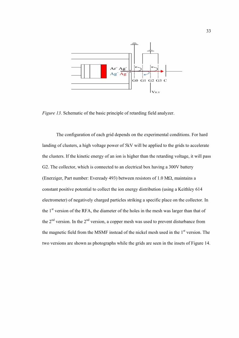
33
Figure 13. Schematic of the basic principle of retarding field analyzer.
The configuration of each grid depends on the experimental conditions. For hard
landing of clusters, a high voltage power of 5kV will be applied to the grids to accelerate
the clusters. If the kinetic energy of an ion is higher than the retarding voltage, it will pass
G2. The collector, which is connected to an electrical box having a 300V battery
(Enerziger, Part number: Eveready 493) between resistors of 1.0 MΩ, maintains a
constant positive potential to collect the ion energy distribution (using a Keithley 614
electrometer) of negatively charged particles striking a specific place on the collector. In
the 1st version of the RFA, the diameter of the holes in the mesh was larger than that of
the 2nd version. In the 2nd version, a copper mesh was used to prevent disturbance from
the magnetic field from the MSMF instead of the nickel mesh used in the 1st version. The
two versions are shown as photographs while the grids are seen in the insets of Figure 14.

34
Figure 14. (a) 1st version and (b) 2nd version of RFA, and their grids shown as insets. The holes on cover of (b) vent the gas mixture to prevent a short circuit at high voltage.
Three-Element Lenses
The Einzel lens is used to focus the charged clusters in flight by manipulating the
electric field in the path of the charged clusters. It consists of a three-element electrode in
which the outer electrodes have the same potential. The number of electrode depends on
the experimental environment. Beam focusing is achieved by changing the potential on
the middle electrode. The kinetic energy of the beam must not be changed while it is
focused. Figure 15(a) and (d) exemplify the focusing effect with different electric fields
on the middle electrode in an Einzel lens using trajectories of charged clusters calculated
using the ion optics simulation program SIMION.66 Figure 15(b) and (c) are different
views of Figure 15(a). The focal point is changed in Figure 15(c) and (d) when a different
electric field is applied to the middle electrode.

35
Figure 15. SIMION simulation of an Einzel lens. (a) cross sectional view of an Einzel lens with electric potential line (red line). Two electrodes are set to ground potential, the middle electrode to +110V. (b) three-dimensional view of the three electrodes and the particle beam. (c) and (d) show focusing effect in a different field of middle electrode. Roll outward shows positive and roll inward indicates negative potential.
Figure 16 shows the Einzel lens used for Matilda. Three cylindrical lenses made
of aluminum were held using a cylindrical piece of ceramic (Mcmaster-carr, Part number:

36
8489K81). The inner diameter of the lenses was 0.5˝ and the thickness of the wall was
0.1˝. The lenses were mounted on ceramic rods 0.2˝ in diameter that insulated the lenses
from one another and from a grounded mounting block and lens holder. The gap between
the electrodes was 0.025˝.
Figure 16. Picture of the three-element lenses used for Matilda.
Magnetic Sector Mass Filter for Mass Separation
According to the principle underlying the MSMF separation of masses in Figure
17, the radius of ion trajectory is proportional to the root of the particle’s mass, m, and V,
which is the retarding voltage provided by the RFA and is inversely proportional to the
magnetic field strength. e is the charge on the mass selected ion.67
emV
BR 21= (8)

37
Figure 17. Schematic of MSMF for mass separation.
In the experiment, two neodymium (NdFeB) block magnets (Kjmagnetics, Inc.,
Part number: BZX0Y08) were used for size separation. Figure 18 shows a picture of the
MSMF, which is enclosed by soft iron (a) to confine the magnetic field. Each magnet was
4˝ width × 2˝ long × 0.5˝ thick. The gap between the magnets was 0.5˝. Aluminum rod
and bolts and nuts were used to adjust the height of the gap with the beam line. Three
pink insulators were used to separate the electrical grounds from each other.

38
Figure 18. Picture of MSMF: (a) cover, (b) neodymium block, (c) pink colored insulator, (d) supporter with bolt and nut, and (e) electrical connector.
Detection Methods of Charged Particle
For charged particle detection, there are two widely used detection methods:
Faraday cup and CEM (see Figure 19). A Faraday cup is a conductive metal cup designed
to collect charged particles in a vacuum. A Faraday cup acts as a collector for electrons
from an electron beam. In this case, electrons simply hit the metal plate or cup and a
current is produced. Faraday cups are not as sensitive as electron multiplier detectors but
are highly regarded for accuracy because of the direct relation between the measured
current and the number of ions. The Faraday cup was used as a collector for Matilda (see
Figure 10.)
(a)
(b)
(c)
(d) (e)

39
Figure 19. Schematics of (a) Faraday cup and (b) CEM for detection of negatively charged ions.
A CEM is a glass tube with semiconducting inner surfaces that multiply incident
particles. Incident particles must have an excess energy to ensure efficient secondary
electron emission because semiconducting inner surfaces are made of materials with a
high work function to inhibit thermionic emission that would increase noise at the
multiplier output. On the other hand, when working with lower energy particles, it is
necessary to provide an acceleration stage at the multiplier input. For positive ions, the
input is generally at a negative potential of 1000 volts; output is normally grounded. For
detection of negative ions, the input is normally grounded or at some positive potential,
and the output is at a high positive voltage.68, 69 Figure 20 shows the current CEM setup
with a discriminator to obtain the charged cluster signals.

40
Figure 20. The circuit of CEM with discriminator (AMPTEK A101 and PC-10 board).
For the detection of negative charged particles in Matilda, CEM (Burle Model
No: 4774) was used and installed downstream of the MSMF. An AMPTEK A101 is used
for the preamplifier and for removing noise from the discriminator. At the multiplier
input, the potential (200V) repels positively charged particles and only accepts negatively
charged particles. They were accelerated by high voltage (2.5kV), which achieved the
saturated signal. The PC-10 board sent the signal to the ORTEC 661 ratemeter, which can
produce an analog signal in the 0-10V range.

41
Modification of Nanocluster Source
After testing the 1st version of the nanocluster source, an electrical feedthrough, a
pumping port, and a shortened aggregation tube length was added. The schematics of the
1st and 2nd version of the cluster source are shown in Appendices A and B. During
deposition of the 1st version of the cluster source, target material was deposited on the
side wall of the aggregation tube, as shown in Figure 21(a). Next, the pumping port was
added behind the aggregation tube to easily evacuate all contaminants, as shown in
Figure 21(b). The electrical lines for the RFA were cumbersome to connect when the
cluster source was dismounted from the chamber. All electrical lines ran through the
aggregation tube and were connected with feedthrough connectors (Ceramtec, Part
number: 9791-08-W) in the aperture, shown in Figure 21(c) and (d). The 1st cluster
source produced particles in the 20 to 80nm range at a 4˝ aggregation distance. A major
goal for catalysis is to produce particle sizes from atomic scale to 10nm. Therefore, the
aggregation tube length was shortened from 10˝ to 8.5˝, as shown in Appendix A.

42
Figure 21. The pictures of the modification of the 1st version cluster source. (a) Deposited place after deposition, (b) pumping port and feedthrough for RFA, and electrical line with (c) 1st and (d) 2nd versions of the RFA.

43
CHAPTER V
PERFORMANCE OF MATILDA
The range of cluster sizes produced can be varied by changing parameters such as
gas pressure, aggregation distance, and sputter power. The pressures of Ar and He are
most effective for controlling cluster size. If calculated correctly, these parameters will
produce clusters which have a proper range of cluster size, from a few atoms to a few
thousand atoms per cluster, depending on the target material.51 Figure 22 shows the High
angle annual dark field (HAADF) image and the spectra from XPS and EDX analysis to
confirm the deposited materials. Binding energy of Ag is lower than that of pure silver
(B.E:368.4eV) due to contaminations of breaking vacuum and deposition. Blank data of
EDX analysis in Figure 22 has low intensity than that of Ag on C-TEM grid because
blank data was collected at low magnification. Particle size distribution was measured by
NIS-Element BR (Version 2.20, Nikon Instruments Inc.) from the TEM images and the
Nanoscope (Version 5.12r4, Digital Instruments). Experiments were performed with RFA.
Pressure Ratio of Helium to Argon
First, the Ar flow rate was varied to find the conditions which could produce
small clusters. Then, He was increased to obtain the desired cluster size. Changing the
ratio of He to Ar pressure has a marked influence on the mean particle size, as shown by
TEM in Figure 23. At a 14sccm Ar flow rate, the range of particle size was 20 ~ 80nm

44
(not shown) and was 1.5 ~ 8nm at 0.4sccm Ar, which is the minimum flow rate for
sputtering. At a zero pressure ratio, the pressure on the aggregation tube was 70mtorr.
Changing flow rate conditions generated a wide range of cluster sizes. The mean size of
the particles was dramatically decreased by increasing the He pressure in the gas mixture.
Clusters of 0.5 ~ 4.0nm in size were produced when the pressure ratio was 9.5. The mean
size of these clusters was 1.6nm. The effect of He gas pressure is the most important
factor for producing small particles. Figure 24 shows that the He flow rate not only
decreased the particle size distribution, but also decreased the width of the distribution
peak. At a low pressure ratio, the size distribution was broad, from small clusters to large
clusters. As large clusters deposited on TEM grid start to agglomerate each other during
long deposition time and they become peanut shape. Most of large clusters are
polycrystalline. For small clusters which are less than 2nm in size, high resolution TEM
hardly provides a clear image. In this range of cluster size clusters have single crystalline
and polycrystalline. The crystalline effect of cluster for chemical activity wasn’t tested.

45
0 5 1 0 1 5 2 0
(b )
C C uA g
A g /C -T E M g r id
Inte
nsity
(arb
. uni
ts)
E n erg y (k eV )
B la n k
3 7 6 3 7 2 3 6 8 3 6 4
Inte
nsity
(arb
. uni
ts)
B in d in g e n e r g y ( e V )
A g 3 d
3 6 8 .0 2 e V
(C )
Figure 22. (a) HAADF image, (b) EDX analysis of Ag on c-TEM grid in red circle area of (a), and (c) XPS spectra of Ag/Si. Red lines are for Ag and black lines are for substrate.

46
Figure 23. TEM images of Ag on c-coated grid with RFA as pressure ratio of He to Ar (a) 0, (b) 2.5 (c) 4.5, (d) 6, and (e) 9.5 at 2˝ aggregation distance and 20 minutes deposition.

47
0 2 4 6 8 10 120
10
20
30
40
50
60
70
0.0 2.5 4.5 6.0 9.5
Freq
uenc
y (%
)
Particle size (nm)
Pressure ratio (He/Ar)
Figure 24. Particle size distribution from Fig. 23.
Two growth modes; two body (cluster collision) and three body collision (two
sputtered atoms collide with He, removing the excess kinetic energy of the sputtered
atoms), simultaneously occur in this condition. At a high pressure ratio, three body
collision dominates to produce small clusters.51 Thus, He promotes the growth of small
clusters from a few atoms at a high pressure ratio. A higher cluster current was obtained
with a decreasing pressure ratio as shown in Figure 25.

48
0 2 4 6 8 10 120
-2
-4
-6
-8
-10
Ion
curr
ent (
μA)
Pressure ratio (He/Ar)
-6.5μA
-50nA
Figure 25. Saturation ion current vs. pressure ratio (He/Ar) at 20 watt sputter power (Pressure ratio = 0 (only 0.4 sccm of Ar)).
This means that charged clusters left the skimmer more efficiently, with a higher partial
pressure of Ar and a low partial pressure of He. Only a small amount of clusters were
skimmed out, because most of the sputtered clusters had a short mean free path and were
deposited on the aggregation tube wall. For this reason, particles are not seen at a
pressure ratio of 12; however, an ion current is detectable as the increasing He flow
decreases the ion current from -6.5μA to -50nA as seen in Figure 25. The Ag peak on the
TEM grid was not seen using XPS at a pressure ratio of 12.

49
Ion Energy Distribution
The sputter gun power supply was regulated, that is, both the voltage and current
were increased in correct proportion to maintain a constant power during the deposition.
This ensured that the flux of atoms leaving the source remained constant. Changing the
target voltage had a direct influence on the measured ion energy distribution curves. Ion
energy distribution is presented as dI/dV, as current decreased when the retarding voltage
was increased. The ion energy distribution slightly increased with increasing sputter
power, as shown in Figure 26. As the ions diffused through the aggregation region, they
lost some of their kinetic energy. Since the sputter target was moveable in the cluster
source, the length of the aggregation region could be changed. The ion energy
distribution decreased with increasing aggregation distance; the number of clusters
decreased by collision and deposition in the aggregation tube, as shown in Figure 27.
Thus, the mean particle size increased beyond 20nm at 4˝ and up to 80nm at 6˝
aggregation distance. Also, the number of particles decreased with increasing aggregation
distance. The ion energy distribution decreased with increasing He flow rates due to more
collisions as shown in Figure 28. The cluster landing energy could be predicted by the ion
energy distribution, and would determine if the clusters had been deformed or not during
deposition. Figure 29 shows the ion energy distributions of different acceleration voltages
at a zero pressure ratio and at 0.4 sccm Ar with 20 watt sputter power and a 2˝
aggregation distance. The peaks widen with an increasing acceleration voltage, which
may allow the separation of ions with mass occupying high energy regions and high mass
occupying low energy regions. As the acceleration voltage was increased, the ion energy
distribution started to stretch out on the positive side of the retarding voltage. However,

50
the reason for this was unclear. The degree of stretching depended on the acceleration
voltage.
20 10 0 -10 -20 -300
-1
-2
-3
-4
-5
-6
-7
5W(290V) 10W(330V) 20W(385V) 50W(450V)
dI/d
V (μ
A/V
)
Retarding voltage (V)
Sputter power(target voltage)
Figure 26. Ion energy distribution with different sputter power at 2˝ aggregation distance and 0.4 sccm Ar flow rate (solid line is the indicator of the center of ion energy distribution).

51
20 10 0 -10 -20 -300
-1
-2
-3
-4
-5
20 10 0 -10 -20 -300.0
-0.1
-0.2
-0.3
-0.4
dI/d
V (μ
A/V
)Retarding voltage (V)
2" 4" 6"
dI/d
V (μ
A/V
)
Retarding voltage (V)
Aggregation distance
Figure 27. Ion energy distribution with different aggregation distances at 20 watt sputter power and a 0.4sccm Ar flow rate.

52
10 5 0 -5 -10 -15 -200.0
-0.5
-1.0
-1.5
-2.0
0.0 2.5 4.5 6.0 9.5 12.0
dI/d
V (μ
A/V
)
Retarding voltage (V)
Pressure ratio (He/Ar)
Figure 28. Ion energy distribution with different He flow rates at 0.4 sccm Ar with 20watt sputter power and 2˝ aggregation distance.

53
20 10 0 -10 -20 -300.0
-0.2
-0.4
-0.6
-0.8
-1.0
No Acc 200 500 1000
dI/d
V (μ
A/V
)
Retarding voltage (V)
Acceleration voltage (V)
Figure 29. Ion energy distribution with different acceleration voltages at a zero pressure ratio and at 0.4 sccm Ar with 20 watt sputter power and 2˝ aggregation distance. G1and G2 are applied with an acceleration voltage and G3 is the retarding grid.
To understand this phenomena, a retarding test with particle size distribution may
be required. Voltage leaking occurred at a high acceleration voltage (2.0kV), perhaps
caused by the ionization of the gas mixture. Maximum cluster landing energy, which is
the maximum ion energy (Figure 26) per minimum cluster size (Figures 23 and 24), was
calculated as reported in Appendix H. At a zero pressure ratio, in Figure 30, the
maximum landing energy was ~ 2.9eV/atom, which was higher than in the soft landing
condition (≤0.1eV/atom),30, 70 because there was a single negatively charged ion and a
spherical particle. Most clusters will be soft landed during deposition. To accurately
verify landing energy, further analysis with a scanning tunneling microscope would be
needed to acquire three dimensional images of the clusters.

54
0 2 4 6 8 100.01
0.1
1
10
102
103
104
105
Max
. lan
ding
ene
rgy
(eV
)
Pressure ratio (He/Ar)
Num
ber
of a
tom
s
Figure 30. Maximum cluster landing energy at different pressure ratios (He/Ar).
Ion Optics for Retarding Field Analyzer
The RFA was designed to suppress the beam expansion, to some extent, after
skimming. Cluster beam size was measured by the mark on the colloidal graphite-coated
Cu plate used as a collector grid without and with RFA after deposition. Without the RFA,
the beam size was about 0.74˝. The size of the cluster beam was about 0.18˝ in diameter
at the collector grids and 0.28˝ from the collector grid of the RFA. Beam intensity was ~ -
1206.0μA/in2 at a zero pressure ratio. Beam intensity decreased with increasing pressure
ratios due to the decreasing number of ions from the cluster source, shown in Figure 25.
Figure 31(a) shows the schematic of the RFA by SIMION 3D coding and the
magnification of the copper mesh. A 100% transparent ideal grid was used during the
simulation without ceramic spacers due to the reduction of beam transmission.71 Each of
55
the RFA could be biased with negative voltages for the deceleration of particles, or a
positive voltage could be applied for the acceleration of negative ions, and with opposite
voltages on the grids to prevent the deposition of Ar+ ions and positively charged silver
clusters on the substrate. Neutral clusters cannot be removed in this experiment. Only
ions having a higher energy than the retarding voltage at the G2 grid can pass and are
deposited on the substrate in Figure 31(b) and (c). Some ions evacuated from the
skimmer cannot pass the RFA by the initial beam position; however, the kinetic energy of
the beam is higher than the retarding voltage in Figure 31(b) and (c). The ions
represented by the red and green lines are different in their incoming position for the
RFA, but neither can pass the retarding grid. The incoming position of the ion may also
influence the ion current. The ion current depends on the number of negatively charged
particle hitting the collector. It increases with an increasing acceleration voltage to
promote the hitting rate of ions and decreases with increasing retarding voltage to prevent
passing ions at the retarding grid, shown in Figure 32(a). The number of particles from
Figures 33 and 34 follows the same trend as the ion current in Figure 32(a).

56
Figure 31. (a) Five grids and ceramic spacer in retarding field analyzer with magnification of 100% transparency copper mesh (real grids have 80% transparence) of each grid. (b) Beam trajectories for retarding voltage (-5V) at G2 (200V). Initial K.E of black and red line = 5eV, and other lines have 6eV. (c) Beam trajectories for retarding voltage (-9V) at G2 (200V). Initial K.E of black and red line = 9eV and other lines have 10eV. Sample holder is grounded.
(a)
(b)
(c)

57
5 6 9 10
0.0
-2.5
-5.0
-7.5
-10.0
6 9 100
400
800
1200
Ion
curr
ent (μA
)
No retarding Retarding:-5V Retarding:-9V Acc (G1):+200V
(a) No retarding Retarding:-5V Retarding:-9V
Num
ber
of p
artic
le
Pressure ratio (He/Ar)
(b)
Figure 32. (a) Ion current and (b) number of particles collected from TEM images
To verify the cluster ion energy for large and small clusters at 6.0 and 9.5 pressure
ratios in Figures 33 and 34, the retarding grid was applied with -5 and -9V to compare
with a control condition with no retarding. The results did not clearly verify the retarding
effect because both large and small cluster existed in the same images. Also, size
distribution had no distinct trend in Figure 33, although Figure 34 shows a trend in size
distribution.

58
Figure 33. TEM image and particle size distribution at -5V of retarding voltage with a 6.0 pressure ratio at G1=+200V. Other grids and sample holder are grounded.
0 2 4 6 8 10 120
10
20
30
40
50
60
70 No retarding Retarding : -5V Retarding : -9V
Freq
uenc
y(%
)
Particle size (nm)

59
Figure 34. TEM image and particle size distribution at -9V of retarding voltage with a 9.5 pressure ratio at G1=+200V. Other grids and sample holder are grounded.
0 2 4 6 8 10 120
20
40
60
80
100 No retarding Retarding : -5V Retarding : -9V
Freq
uenc
y(%
)
Particle size (nm)

60
CHAPTER VI
PROGRESS OF SIZE SELECTION OF CLUSTER
Beam Profile
Previously, a Ag target was used to deposit clusters on carbon-coated TEM grids
downstream of the MSMF for two hours at the zero pressure ratio with 20 watts of sputter
power, but particles were not seen on the grids with TEM and XPS. Therefore, during the
experiment and simulation, the hole size of the collector was increased from 0.04˝ to
0.16˝ in diameter. The cluster beam profile was measured at 0.15˝ from the end of the
Einzel lens and 1.4˝ from MSMF downstream by moving the CEM, which gives the ion
voltage. For this experiment, clusters were produced at a zero pressure ratio of He to Ar,
which was desirable to produce cluster sizes from the atomic scale to 10nm. To minimize
beam divergence at the end of the lens, SIMION shows the best value of the potential on
each electrode. When the middle electrode (V2) was 100V, shown in Figure 35, there
was not a lot of divergence in the beam. Although the beam was well focused at the end
of the lens in other conditions, it started to expand through the MSMF. Beam divergence
can inhibit size selection of clusters at some positions and makes the selection area small.
For simulation, the initial beam spread was set at 0.08˝ in diameter with an entrance angle
of 12.4°, which is the same value of outlet angle in aperture shown in Appendix D. The
energy of a 2nm cluster is 4eV from Figure 26. The distance between the starting beam

61
position and the RFA is 0.7˝, which is the real distance according to Appendix D. The ion
voltage distribution of the experiment was broader.
Figure 35. RFA and three-element lenses in SIMION for the potential setting. G0: ground, G1~ C: +20V, V1 and V3: +20V, and V2: +100V. This condition makes the beam spread the least after passing the lens.
Figure 36. (a) The distribution of ions from the simulation and (b) simulated and experiment at 0.15˝ from lens. The ion beam is approximately 0.2˝ in diameter. Blue line in (a) is the beam profile line for (b). Deflector can shift the experimental peak to the simulation result.
-0.4 -0.2 0.0 0.2 0.40.0
0.2
0.4
0.6
0.8
1.0 simulation measured
Nor
mal
ized
ion
flux
detector position (inch)
Deflection
(b)

62
Although the beam was not centered on the lens, the simulated result was similar
to the experimental trend. The position of the beam could be shifted by a deflector made
of four electrodes, which changed the center of the beam by applying an electric potential
at different electrodes. The data in Figure 37 using a CEM also shows that the beam
spread is almost three times as big as the beam size in Figure 36. SIMION was used to
model two separate simulations, because it cannot manipulate two different potentials at
the same time, such as the electric and magnetic potentials.
Figure 37. The ion beam profile of 1.4˝ distance from MSMF. Beam diameter is 0.7˝.
Figure 38 shows the beam spread superimposed on the magnetic sector to verify
the size-selection region. The size-selection region decreases as the distance from the
MSMF decreases. Sample substrate and CEM must be installed as close as possible
-0.4 -0.2 0.0 0.2 0.4
0.0
0.2
0.4
0.6
0.8
1.0
Nor
mal
ized
ion
flux
CEM position (inch)

63
behind the MSMF. A new lens had to be redesigned to make a well-focused beam
through the MSMF.
Figure 38. The real area for size selection after MSMF. Beam diameter is 0.5˝ and 0.7˝ from direct behind and 1.4˝ from MSMF. Yellow color is magnet and gray color is the cover of magnets. CEM must be installed as close as possible to increase selection region. Six TEM grids (from 0 to 5 in red circle) were installed at the end of MSMF at intervals of 0.5˝. TEM grid (0 in red circle) is neutral position.
Magnetic Field Distribution in Magnetic Sector Mass Filter Figure 39(a) shows the distribution of measured magnetic fields in the MSMF. The
magnetic field was measured by a gauss probe (Lake Shore Cryotronics, Inc., Model 410)
at the center position of the gap between two magnets by a 0.25˝ and 0.1˝ distance from
the z-axis and x-axis, respectively. At only 3˝ and 1˝ from the z-axis and x-axis was an
almost even magnetic field. The Lua program72 was introduced to the measured field of
the MSMF to apply the same magnetic field in simulation. SIMION brought only one
dimensional (y-axis) magnetic field, because three-dimensional magnetic fields could not

64
be obtained. The measured magnetic field was similar to the simulated field in Figure
39(b).
Figure 39. Comparison between (a) real magnetic field and (b) simulated magnetic field. Red line is the size of magnet. Both show the magnetic field without magnets.
The magnetic field was not completely even in the MSMF. It was almost even
through the z-axis direction but had a 1˝ range in the x-axis direction. The beam was
introduced at a -1.0˝ position at the x-axis. Although the area outside of the field was
defined by the measured magnetic field, SIMION assumed the fields were zero. Ion
trajectories may not be realistic outside of the region.
Size Selection of Cluster
Ion trajectories of different kinetic energies of mass were estimated by SIMION.
Figure 40 shows the ion trajectories with different kinetic energy conditions. This helps
in evaluating the capability of the MSMF.
-2 -1 0 1 2
-2
-1
0
1
2
X-a
xis (
inch
)
Z-axis (inch)
0.010.100.20.30.40.40.50.60.7
B-field (T)
(a)
-2 -1 0 1 2
-2
-1
0
1
2
X-a
xis (
inch
)
Z-axis (inch)
00.090.20.30.30.40.50.60.7
B-field (T)
(b)

65
Figure 40. Ion trajectories of (a) 30eV kinetic energy for low mass (≥ 2.0nm), (b) 4eV for the zero pressure ratio, and (c) 1eV kinetic energy for high mass (≤ 2.0nm).
In the previous acceleration experiment shown in Figure 29, the ion energy
distribution only goes up to 30V and is not enough to separate clusters less than 1.0nm.
As a simulation result, the range of size selection is from 0.67nm (13atoms) to 3.0nm
(1120atoms). A better RFA design would be required to control the cluster energy.
Before obtaining the ion signal downstream of the MSMF with CEM, the ORTEC 661
ratemeter was set to an optimal threshold to prevent dark current signals, which lead to
wrong signals from the CEM, and to 5000 count/sec of full scale range, fast response, 1x
multiplier, and 0 ~ 10V of analog output, which was collected by LabVIEW. An
oscilloscope also confirmed whether the signals came from the clusters or not. Sixteen
data points were collected 10 sec/each position at 1.4˝ distance from MSMF, as seen in
Figure 41.

66
05
10
0.00.20.4
0.00.20.4
0.00.20.4
0.00.20.4
0.00.20.4
Collection time (full range :10 sec)
Ion
volta
ge in
tens
ity (V
)
0.0" position
0.5" position
1.0" position
1.5" position
2.0" position
2.5" position
Figure 41. CEM data of Ag clusters at different positions.
At the 0˝ position of the CEM, the cluster signal was almost constant, unlike
other positions, which had only a few signals with low ion voltage intensity. There were
many large clusters as well as neutral clusters. Figure 42 shows the normalized ion
voltage signal from Figure 41. From 0 (neutral cluster region) to 0.25˝, the cluster signal
was almost constant. Then, the cluster signal dramatically deceased and was almost
constant because only a few clusters hit the CEM, as seen in Figure 41.

67
0 1 2 3 40.0
0.2
0.4
0.6
0.8
1.0
Nor
mal
ized
ion
flux
CEM Position (inch)
x10
Figure 42. CEM spectrum of negatively charged Ag nanoparticles. 0 position of CEM is for neutral and large clusters. All signals of positions are averaged and normalized from the previous figure.
Before deposition, The MSMF and TEM grids was applied with the same
potential, with V3 of lens (Figure 35) to remove the retardation of clusters on six TEM
grids installed at intervals of 0.5˝ as seen in Figure 38. Two Ag targets were sputtered at a
zero pressure ratio for four and a half hours. Before obtaining TEM images, the existence
of Ag clusters on the TEM grids was tested by XPS. Only two TEM grids (neutral and
0.5˝ position) had an XPS signal and were imaged by TEM. The results of the size
selection of Ag clusters are shown in Figure 43 for the neutral position and in Figure 44
for the 0.5˝ interval. The particle size in Figure 43 has two different ranges: one area has
only clusters ranging from 1.0 to 2.5nm and other areas have a wider cluster range, from
0.9 to 7.0nm. Figure 44 depicts cluster sizes ranging only from 0.8 to 2.2nm, which is

68
similar to one area seen in Figure 43. The cluster sizes at the neutral position ranged from
0.8 to 7.0nm, as seen in Figure 43. By the trajectory simulation, clusters from 1.7 to
2.5nm having from 5 to 15eV passed through the 0.5˝ position in the MSMF. For the
simulation, this range of kinetic energy of clusters was well matched with Figure 26.
Although images show uniformly sized clusters, Figure 44 was not fully supported for
size selection because the neutral clusters passed the 0.5˝ position in Figure 38. More
deposition for verifying size selection may be required.
Figure 43. Ag clusters on the TEM grids at the neutral position.

69
Figure 44. Ag clusters on the TEM grids at the 0.5˝ position.
2nd Version of Lens for Focusing Beam
In the previous three-element lens pictured in Figure 38, the charged beam started
to spread when the beams left the electric field. To minimize the spread of the beam, a
new three-element lens was modified in the first (V1) and last tube (V3) in Figure 45 and
Figure 46(a). For the first tube, its conical shape played a role in minimizing beam spread
after the third lens. The third tube had a beam guider, a small-sized tube to be introduced
directly into the gap of the magnetic sector. The beam guider can be placed on the inside
edge of the MSMF.

70
Figure 45. 2nd version of three-element lens. a is the holder for installation on the cluster source. b is the electrical connector. c is the holder for fixing three tubes (V1, V2, and V3). d is the ceramic rod from electric field. e is the hole for threaded rods which are connected with cluster source. g is the beam guider.
When the 2nd version of the lens was designed, beam transmission was considered in
order to deal with its spread. If the hole of the conical tube is large, beam transmission is
good at the hole of the conical tube, but the spread gets worse downstream in the third
tube. Figure 46(b) and (c) show the beam trajectories at low and high electric fields. Both
beam diameters in the MSMF were well focused and not spread. For this simulation, the
initial beam spread and entrance angle were set to the same value in Appendix D. 30,000
particles which have a negatively charged silver ion of 2nm in diameter were sent into the
RFA, and then the beam transmission was calculated by the number of ions passing RFA
and lens. The transmission percentage of the ions was about 65% from the end of the
RFA to the end of the guider in Figure 45(b). At high voltage, beam transmission goes
down to 15%. A long deposition time was required to get a high enough number of

71
clusters. Ion current after RFA and lens may be required to find proper deposition time.
The 2nd version of the lens will be tested soon.
Figure 46. (a) 2nd version of Einzel lens to minimize the beam spread including g, beam guider. (b) Beam trajectory at V1 and V3 = +20V, V2 = +100V. (c) Beam trajectory at V1 and V3 = +1.0kV, and V2 = +2.0kV.

72
CHAPTER VII
CONCLUSION AND FUTURE WORK
Conclusions
Nanoclusters have recently received a tremendous amount of attention because of
their fundamental importance in chemistry and physics for application in catalysis and
nanotechnology. Cluster properties can be changed by controlling the size of the cluster.
Current mass filters, which are wien velocity, time of flight, quadruople, and magnetic
sector mass, have a limited range of mass selection. A new mass filter is required for a
high-flux beam of clusters that can separate clusters up to 10nm in diameter without
sacrificing its resolution.
In this experiment, Matilda was designed for the deposition of size-selected
nanoparticles ranging from atomic scale to 10nm. Matilda has a nanocluster source (1st
and 2nd version) based on magnetron sputtering, an RFA (1st and 2nd version) providing
ion energy distribution information, a three-element lens to focus and introduce beams
into the MSMF, and an MSMF for size separation up to 3nm. For testing size distribution,
nanoclusters were deposited on carbon-coated TEM grids with different pressure ratios
between He and Ar. Size distribution varied from 10nm to 0.5nm by increasing the
pressure ratio. At the highest pressure ratio, size distribution was much more narrow than
at the low pressure ratio. This means that pressure ratio can control size selection up to
4nm, although 4nm in diameter has a size variation of ±2nm. The RFA collected ion

73
energy distribution with different sputter powers, aggregation distances, pressure ratios,
and acceleration voltages. The ion energy distribution increased with increasing sputter
power because of the increase in ion flux. With increasing aggregation distances, the ion
energy distribution and flux decreased, because kinetic energy was lowered by many
body collisions before the skimmer. Increasing the pressure ratio decreased ion energy
and flux. When grids were applied with a high voltage, the ion energy distribution
broadened. An acceleration voltage may allow separation between low mass occupying
high energy regions and high mass occupying low energy regions. To understand the
stretching of ion energy distribution, further tests varying the retarding voltage are
required for determining the correlation between mass and acceleration. Most of clusters
were deposited on the substrate with soft landing (≤0.1eV kinetic energy). Only at a zero
pressure ratio of He/Ar was the maximum landing energy higher than that of the soft
landing. Further analysis with scanning tunneling microscope is needed to acquire three-
dimensional images of clusters which would verify the soft and hard landing cluster cases.
The retarding effect was demonstrated by SIMION, as well as experiments to verify the
design of ion optics of the RFA. This effect clearly shows the number of transmitted
clusters, which was decreased by increasing the retarding voltage; however, the particle
size distribution could not clearly be explained because of the outlier effect of neutral
clusters.
For the size selection experiment, the three-element lens, the MSMF, and the
CEM were installed in the chamber. The three-element lens produced the narrow-sized
and focused beam for the MSMF. The beam profile was about 0.25˝ at the end of the lens
and 0.7˝ from a distance of 1.4˝ from the MSMF. The simulation result was well

74
matched to the experimental results. The real magnetic field was introduced into SIMION
by the Lua program for simulating similar conditions. The results agreed with the real
magnetic field. The CEM collected cluster signals at different positions, and a Ag target
was used to deposit clusters on the TEM grid for four and a half hours. The cluster signal
was high from the 0 to 0.25˝ position, but the signal decreased rapidly far away from the
neutral cluster region. By simulation and TEM images, size selection was verified, but
more testing may be required because of the beam spread. For cluster separation
according to mass-to- charge ratio in the MSMF, the ion energy of the clusters and their
distribution must be precisely controlled by acceleration or deceleration. Finally, Matilda
provided narrow particle sized distribution from atomic scale to 4nm in size with
different pressure ratio without additional mass filter. It is very economical way to
produce relatively narrow particle size distribution.
Future Work
The cluster source of the 2nd version still has difficulties in the line connection of
the RFA. Electrical connectors need to be installed on flange. Also, a translator is needed
to adjust the aggregation distance without breaking the vacuum. The RFA may not only
require an increased copper mesh diameter to accelerate clusters and control ion energy
efficiently, but also require many holes to exhaust gas mixtures to prevent a short circuit.
Also, a high mass flow rate with several stages of a differential pumping system is
helpful for increasing the ion energy distribution effectively. For beam focusing, the lens
requires longer and bigger diameters and a deflector to shift the center of the beam to the
center of the lens. The simulation will be required to find the proper sizes of lens and

75
deflector. For high mass filtering, the cluster system requires a large magnet to obtain a
high magnetic field which is up to 1.5T. The additional setup required may add to the
cost of the experiment. However, these adjustments are not the final solution for building
a size-selected cluster system for the high mass region. To control particle size
distribution up to the 10nm regime, a new system consisting of two mass filters, such as a
QMF and PFMS, is required. The QMF is suitable for low mass regions with high
resolution, and the PFMS is desirable for high mass regions with a simple design, high
transmission, and fairly good mass resolution. For this system, a quadrupole deflector is
required to send beams to the QMF and PFMS.

76
REFERENCES
1. See, U.S. Department of Energy Hydrogen, Fuel Cells and Infrastructure Technologies Program Multi-Year Research, Development and Demonstration Plan, U.S Department of Energy; http://www1.eere.energy.gov/hydrogenandfuelcells/ (2007).
2. Chalk, S. G.; Miller, J. E., Key challenges and recent progress in batteries, fuel
cells, and hydrogen storage for clean energy systems. Journal of Power Sources 2006, 159, (1), 73-80.
3. Antolini, E., Formation, microstructural characteristics and stability of carbon
supported platinum catalysts for low temperature fuel cells. Journal of Materials Science 2003, 38, (14), 2995-3005.
4. Ertl, G.; Knozinger, H.; Weitkamp, J.; Shchuth, F.; Weitkamp, J., Handbook of
Heterogenous Catalysis, Vol. 1 1997, second ed. (Wiley-VCH, 2008). 5. Moulijn, J. A.; van leeuwen, P. W. N. M.; van Santen, R. A., Catalysis: An
Integrated Approach to Homogeneous, Heterogeneous and Industrial Catalysis, (Elsevier Science, Amsterdam, 2002).
6. Kasemo, B.; Johansson, S.; Persson, H.; Thormahlen, P.; Zhdanov, V. P.,
Catalysis in the nm-regime: manufacturing of supported model catalysts and theoretical studies of the reaction kinetics. Topics in Catalysis 2000, 13, (1-2), 43-53.
7. Song, H.; Rioux, R. M.; Hoefelmeyer, J. D.; Komor, R.; Niesz, K.; Grass, M.;
Yang, P. D.; Somorjai, G. A., Hydrothermal growth of mesoporous SBA-15 silica in the presence of PVP-stabilized Pt nanoparticles: Synthesis, characterization, and catalytic properties. Journal of the American Chemical Society 2006, 128, (9), 3027-3037.
8. Gates, B. C., Models of metal catalysts: beyond single crystals. Topics in
Catalysis 2001, 14, (1-4), 173-180. 9. Somorjai, G. A.; Tao, F.; Park, J. Y., The nanoscience revolution: Merging of
colloid science, catalysis and nanoelectronics. Topics in Catalysis 2008, 47, (1-2), 1-14.
77
10. Liu, Z.; Reed, D.; Kwon, G.; Shamsuzzoha, M.; Nikles, D. E., Pt3Sn nanoparticles with controlled size: High-temperature synthesis and room-temperature catalytic activation for electrochemical methanol oxidation. Journal of Physical Chemistry C 2007, 111, 14223-14229.
11. Liu, Z. F.; Shamsuzzoha, M.; Ada, E. T.; Reichert, W. M.; Nikles, D. E.,
Synthesis and activation of Pt nanoparticles with controlled size for fuel cell electrocatalysts. Journal of Power Sources 2007, 164, (2), 472-480.
12. Zeng, J. H.; Su, F. B.; Han, Y. F.; Tian, Z. Q.; Poh, C. K.; Liu, Z. L.; Lin, J. Y.;
Lee, J. Y.; Zhao, X. S., Pt nanoparticles supported on sandwiched Ru/Carbon nanocomposite as a bimetallic catalyst for methanol electrooxidation. Journal of Physical Chemistry C 2008, 112, (40), 15908-15914.
13. Haruta, M., Size- and support-dependency in the catalysis of gold. Catalysis
Today 1997, 36, (1), 153-166. 14. Valden, M.; Lai, X.; Goodman, D. W., Onset of catalytic activity of gold clusters
on titania with the appearance of nonmetallic properties. Science 1998, 281, (5383), 1647-1650.
15. Valden, M.; Pak, S.; Lai, X.; Goodman, D. W., Structure sensitivity of CO
oxidation over model Au/TiO2 catalysts. Catalysis Letters 1998, 56, (1), 7-10. 16. Haruta, M.; Ueda, A.; Tsubota, S.; Sanchez, R. M. T., Low-temperature catalytic
combustion of methanol and its decomposed derivatives over supported gold catalysts. Catalysis Today 1996, 29, (1-4), 443-447.
17. Wong, K.; Johansson, S.; Kasemo, B., Nanofabricated model catalysts -
Manufacturing and model studies. Faraday Discussions 1996, 105, 237-246. 18. Hwang, K. S.; Yang, M. C.; Zhu, J.; Grunes, J.; Somorjai, G. A., The molecular
mechanism of the poisoning of platinum and rhodium catalyzed ethylene hydrogenation by carbon monoxide. Journal of Molecular Catalysis A-Chemical 2003, 204, 499-507.
19. Eppler, A. S.; Zhu, J.; Anderson, E. A.; Somorjai, G. A., Model catalysts
fabricated by electron beam lithography: AFM and TPD surface studies and hydrogenation/dehydrogenation of cyclohexene plus H-2 on a Pt nanoparticle array supported by silica. Topics in Catalysis 2000, 13, (1-2), 33-41.

78
20. Zhu, J.; Somorjai, G. A., Formation of platinum silicide on a platinum nanoparticle array model catalyst deposited on silica during chemical reaction. Nano Letters 2001, 1, (1), 8-13.
21. Bowker, M., Catalysis resolved using scanning tunnelling microscopy. Chemical
Society Reviews 2007, 36, 1656-1673. 22. Poppa, H., Nucleation, Growth, and Tem Analysis of Metal Particles and Clusters
Deposited in Uhv. Catalysis Reviews-Science and Engineering 1993, 35, (3), 359-398.
23. Thomas, M.; Dickinson, J. T.; Poppa, H.; Pound, G. M., Chemisorption of CO on
Pd particles supported on mica. Journal of Vacuum Science and Technology 1978 15, (2), 568-571
24. Abbet, S.; Sanchez, A.; Heiz, U.; Schneider, W. D.; Ferrari, A. M.; Pacchioni, G.;
Rosch, N., Acetylene cyclotrimerization on supported size-selected Pd-n clusters (1 <= n <= 30): one atom is enough! Journal of the American Chemical Society 2000, 122, (14), 3453-3457.
25. Sanchez, A.; Abbet, S.; Heiz, U.; Schneider, W. D.; Hakkinen, H.; Barnett, R. N.;
Landman, U., When gold is not noble: Nanoscale gold catalysts. Journal of Physical Chemistry A 1999, 103, (48), 9573-9578.
26. Heiz, U.; Sanchez, A.; Abbet, S.; Schneider, W. D., Catalytic oxidation of carbon
monoxide on monodispersed platinum clusters: Each atom counts. Journal of the American Chemical Society 1999, 121, (13), 3214-3217.
27. Lee, S.; Fan, C. Y.; Wu, T. P.; Anderson, S. L., Cluster size effects on CO
oxidation activity, adsorbate affinity, and temporal behavior of model Au-n/TiO2 catalysts. Journal of Chemical Physics 2005, 123.124701-124713
28. Toyoda, N.; Houzumi, S.; Yamada, I., Development of a size-selected gas cluster
ion beam system for low-damage processing. Nuclear Instruments & Methods in Physics Research Section B 2005, 241, (1-4), 609-613.
29. Yamada, I.; Matsuo, J.; Toyoda, N.; Kirkpatrick, A., Materials processing by gas
cluster ion beams. Materials Science & Engineering R-Reports 2001, 34, (6), 231-295.

79
30. Bromann, K.; Brune, H.; Felix, C.; Harbich, W.; Monot, R.; Buttet, J.; Kern, K., Hard and soft landing of mass selected Ag clusters on Pt(111). Surface Science 1997, 377, (1-3), 1051-1055.
31. Carroll, S. J.; Pratontep, S.; Streun, M.; Palmer, R. E.; Hobday, S.; Smith, R.,
Pinning of size-selected Ag clusters on graphite surfaces. Journal of Chemical Physics 2000, 113, (18), 7723-7727.
32. Parent, F.; Tuaillon, J.; Stern, L. B.; Dupuis, V.; Prevel, B.; Perez, A.; Melinon,
P.; Guiraud, G.; Morel, R.; Barthelemy, A.; Fert, A., Giant magnetoresistance in Co-Ag granular films prepared by low-energy cluster beam deposition. Physical Review B 1997, 55, (6), 3683-3687.
33. Lidgi-Guigui, N.; Leung, C.; Palmer, R. E., Weak precursor state binding of
protein molecules to size-selected gold nanoclusters on surfaces. Surface Science 2008, 602, (4), 1006-1009.
34. Sattler, K.; Muhlbach, J.; Recknagel, E., Generation of Metal Clusters Containing
from 2 to 500 Atoms. Physical Review Letters 1980, 45, (10), 821-824. 35. Dietz, T. G., Duncan, M. A., Powers, D. E., and Smalley, R. E. , Laser production
of suptersonic metal cluster beams. Journal of Chemical Physics 1981, 74, (11), 6511-6512.
36. Binns, C., Nanoclusters deposited on surfaces. Surface Science Reports 2001, 44,
(1-2), 1-49. 37. Laaksonen, R. T.; Goetsch, D. A.; Owens, D. W.; Poirier, D. M.; Stepniak, F.;
Weaver, J. H., Supersonic Cluster Source with Mass Selection and Energy Control. Review of Scientific Instruments 1994, 65, (7), 2267-2275.
38. Nakajima, A.; Hoshino, K.; Naganuma, T.; Sone, Y.; Kaya, K., Ionization-
Potentials of Aluminum Sodium Bimetallic Clusters (Alnnam). Journal of Chemical Physics 1991, 95, (10), 7061-7066.
39. Lau, J. T.; Achleitner, A.; Ehrke, H. U.; Langenbuch, U.; Reif, M.; Wurth, W.,
Ultrahigh vacuum cluster deposition source for spectroscopy with synchrotron radiation. Review of Scientific Instruments 2005, 76, (6), 63902-63908.

80
40. Haberland, H.; Karrais, M.; Mall, M., A New Type of Cluster and Cluster Ion-Source. Zeitschrift Fur Physik D-Atoms Molecules and Clusters 1991, 20, (1-4), 413-415.
41. Siekmann, H. R.; Luder, C.; Faehrmann, J.; Lutz, H. O.; Meiwesbroer, K. H., The
Pulsed-Arc Cluster Ion-Source (Pacis). Zeitschrift Fur Physik D-Atoms Molecules and Clusters 1991, 20, (1-4), 417-420.
42. Heiz, U.; Vanolli, F.; Trento, L.; Schneider, W. D., Chemical reactivity of size-
selected supported clusters: An experimental setup. Review of Scientific Instruments 1997, 68, (5), 1986-1994.
43. Baker, S. H.; Thornton, S. C.; Keen, A. M.; Preston, T. I.; Norris, C.; Edmonds, K.
W.; Binns, C., The construction of a gas aggregation source for the preparation of mass-selected ultrasmall metal particles. Review of Scientific Instruments 1997, 68, (4), 1853-1857.
44. Bromann, K.; Felix, C.; Brune, H.; Harbich, W.; Monot, R.; Buttet, J.; Kern, K.,
Controlled deposition of size-selected silver nanoclusters. Science 1996, 274, (5289), 956-958.
45. Smith, R., Clampitt, R., and Lee, M. , Magnetron-based nanocluster source:
capabilities, limitations and future possibilities presented in University of Alabama. 2005.
46. Goldby, I. M.; vonIssendorff, B.; Kuipers, L.; Palmer, R. E., Gas condensation
source for production and deposition of size-selected metal clusters. Review of Scientific Instruments 1997, 68, (9), 3327-3334.
47. Wrenger, B.; MeiwesBroer, K. H., The application of a Wien filter Its mass
analysis of heavy clusters from a pulsed supersonic nozzle source. Review of Scientific Instruments 1997, 68, (5), 2027-2030.
48. Haberland, H.; Karrais, M.; Mall, M.; Thurner, Y., Thin-films from energetic
cluster impact - A feasobility study. Journal of Vacuum Science & Technology A 1992, 10, (5), 3266-3271.
49. Turra, M.; Waldschmidt, B.; Kaiser, B.; Schafer, R., An improved time-of-flight
method for cluster deposition and ion-scattering experiments. Review of Scientific Instruments 2008, 79, (1), 13905-13909.
81
50. von Issendorff, B.; Palmer, R. E., A new high transmission infinite range mass selector for cluster and nanoparticle beams. Review of Scientific Instruments 1999, 70, (12), 4497-4501.
51. Pratontep, S.; Carroll, S. J.; Xirouchaki, C.; Streun, M.; Palmer, R. E., Size-
selected cluster beam source based on radio frequency magnetron plasma sputtering and gas condensation. Review of Scientific Instruments 2005, 76, (4), 45103-45109.
52. Kemper, P.; Kolmakov, A.; Tong, X.; Lilach, Y.; Benz, L.; Manard, M.; Metiu,
H.; Buratto, S. K.; Bowers, M. T., Formation, deposition and examination of size selected metal clusters on semiconductor surfaces: An experimental setup. International Journal of Mass Spectrometry 2006, 254, (3), 202-209.
53. Klingeler, R.; Bechthold, P. S.; Neeb, M.; Eberhardt, W., An experimental setup
for nondestructive deposition of size-selected clusters. Review of Scientific Instruments 2002, 73, (4), 1803-1808.
54. Wucher, A.; Wahl, M.; Oechsner, H., The mass-distrbution of sputtered metal-
clusters .1. Experiment. Nuclear Instruments & Methods in Physics Research Section B-Beam Interactions with Materials and Atoms 1993, 83, (1-2), 73-78.
55. Ayesh, A. I.; Lassesson, A.; Brown, S. A.; Dunbar, A. D. F.; Kaufmann, M.;
Partridge, J. G.; Reichel, R.; van Lith, J., Experimental and simulational study of the operation conditions for a high transmission mass filter. Review of Scientific Instruments 2007, 78, (5), 53906-53912.
56. de Hoffman, E.; Stroobant, V., Mass Spectrometry Principles and Applications,
(John Wiley and Sons, Ltd, 2002). 57. Henderson, W.; Mcindoe, J. S., Mass Spectrometry of Inorganic and
Organometallic Compounds, (Wiley-Interscience, 2005). 58. Moulder, J. F.; Stickle, W. F.; Sobol, P. E.; Bomben, K. D.; Chastain, J.; King, J.,
R. C. , Handbook of X-ray Photoelectron Spectroscopy (Physcal Electronics, Inc. Eden Prairie, MN, 1995).
59. Attard, G.; Barness, C., Surfaces, (Oxford University Press Inc., New York, NY,
1998).
82
60. Williams, D. B.; Carter, C. B., Transmission Electron Microscopy, first ed. (Springer, New York, NY, 2004).
61. Liu, J. Y., Scanning transmission electron microscopy and its application to the study of nanoparticles and nanoparticle systems. Journal of Electron Microscopy 2005, 54, 251-278.
62. Rioux, R. M.; Song, H.; Hoefelmeyer, J. D.; Yang, P.; Somorjai, G. A., High-
surface-area catalyst design: Synthesis, characterization, and reaction studies of platinum nanoparticles in mesoporous SBA-15 silica. Journal of Physical Chemistry B 2005, 109, (6), 2192-2202.
63. Haberland, H.; Mall, M.; Moseler, M.; Qian, Y.; Reiners, T.; Thurner, Y., Filing of
micron-sized contact holes wit copper by energetic cluster-impact. Journal of Vacuum Science & Technology A 1994, 12, (5), 2925-2930.
64. Koch, J., A small retarding field analyzer for Auger electron spectroscopy. Review
of Scientific Instruments 1974, 45, (10), 1212-1213. 65. Bohm, C.; Perrin, J., Retarding-field analyzer for measurements of ion energy
distributions and secondary electron emission coefficients in low-pressure radio frequency discharges. Review of Scientific Instruments 1993, 64, (1), 31-44.
66. Manura, D. J.; Dahl, D. A., SIMION Version 8.0 User Manual, (Scientific
Instrument Services, Inc, USA, Ringoes, NJ, 2007). 67. Tompkins, H. G., Vacuum Gauging and Control, (The American Vacuum Society
Education Committee, New York, NY, 1994). 68. See, Technical Notes, Detector Technology, Inc;
http://www.detechinc.com/notes.htm. 69. See, Channeltron Electron Multiplier Handbook for Spectrometry Applications
Burle Industries, Inc; http://www.burle.com/cgi-bin/byteserver.pl/pdf/ChannelBook.pdf.
70. Haberland, H.; Insepov, Z.; Moseler, M., Molecular-dynamics simulation of thin-film growth by energetic cluster-impact. Physical Review B 1995, 51, (16), 11061-11067.

83
71. Anderson, T. G.; Birdsey, B. G.; Woeher, S. M.; Rosenberry, M. A.; Gay, T. J., A theoretical study of the effects of insulators on electron transport through electrostatic tube lenses. Review of Scientific Instruments 2001, 72, (7), 2923-2925.
72. Ierusalimschy, R., Programming in Lua (Departamento de Informatica, PUC-Rio, Brazil, Rio de Janeiro, 2006).

84
APPENDIX A
SCHEMATICS OF NANOCLUSTER SOURCES
1st Version

85
2nd Version

86
APPENDIX B
PERFORMANCE OF 1ST VERSION OF NANOCLUSTER SOURCE
First we strove to find the conditions for controlling the size of the nanoclusters,
but we did not have much time to test it thoroughly because it had some problems. Test
results were introduced with the AFM and TEM.
AFM Images (Image Scale: 1×1μm)
Sample 12

87
Sample 17
Sample 23
Sample 30

88
Sample 31
Experimental Conditions
Gas flow rate (sccm) Sample
Sputter power (watt) Ar He
Pressure(torr)
Dep.time (min)
Agg. Distance
(inch) RFA
12 10 14 0 6.0×10⁻⁴ 10 4 Yes
17 50 14 0 5.8×10⁻⁴ 10 2 No
23 50 7 0 2.1×10⁻⁴ 3 4 No
30 50 14 14 5.9×10⁻⁴ 10 2 No 31 10 0.4 14 5.3×10⁻⁴ 20 2 No
∗ Pressures are not much different due to main chamber pressure.
Particle Size Distribution
Sample Range of particle size (nm)
12 25 ~ 65 17 25 ~ 80 23 40 ~ 70 30 10 ~ 55 31 35 ~ 70

89
TEM Images
Increasing the He flow rate narrowed the size distribution of the Ag nanoparticles
deposited on the carbon-coated TEM grid.
Sample 33
Sample 34

90
Sample 37
Experimental Conditions
Gas flow rate (sccm) sample
Sputter power (watt) Ar He
Pressure(torr)
Dep.time (min)
Agg. Distance
(inch) RFA
33 50 0.212 0 1.0×10⁻⁵ 10 2 No
34 50 0.217 5 2.4×10⁻⁵ 10 2 No
37 50 0.217 14 4.6×10⁻⁵ 10 2 No
∗ Pressures are not much different due to main chamber pressure.

91
Particle Size Distribution

92
APPENDIX C
ION ENERGY DISTRIBUTION OF 1ST VERSION RFA
An increasing sputter power increased the center peak of the ion energy
distribution, and an increased aggregation distance decreased cluster ion flux.
Figure 47. Ion energy distribution at 4˝aggregation distance.

93
Figure 48. Ion energy distribution at 6˝aggregation distance.
Figure 49. Ion energy distribution at 8˝aggregation distance.

94
APPENDIX D
SCHEMATIC OF APERTURE

95
APPENDIX E
LABVIEW PROGRAMMING
Depositer of Nanoclusters

96
Analyzer for Measuring Ion Energy Distribution
Detector for Measuring Ion Voltage Signal from CEM.

97
APPENDIX F
SIMULATION CODING FOR RFA AND LENS
; RFA and 1st version lens system with deflector ; with housing electrode ; by GiHan Kwon, 1-3-2009 pa_define(520,130,130,p,n) ;======================================== ; housing elemet E1 in Fig.1a of RSI 2008 ;======================================== locate(0,65,65,,,,0) e(1)rotate_fill(360)withinbox(27,62,140,54) ;================================================= ;Five grids electrodes ;================================================= ;================================================= ;Grid 0 : always grounded ;================================================= locate(0,65,65,,,,0) e(2)rotate_fill(360) withinbox(37,42,45,11) withinbox(41,11,41,0) ;================================================= ;Grid 1 ;================================================= locate(0,65,65,,,,0) e(3)rotate_fill(360) withinbox(57,42,65,16) withinbox(61,16,61,0)

98
;================================================= ;Grid 2 ;================================================= locate(0,65,65,,,,0) e(4)rotate_fill(360) withinbox(77,42,85,16) withinbox(81,16,81,0) ;================================================= ;Grid 3 ;================================================= locate(0,65,65,,,,0) e(5)rotate_fill(360) withinbox(97,42,105,16) withinbox(101,16,101,0) ;================================================= ;Grid 4: collector ;================================================= locate(0,65,65,,,,0) e(6)rotate_fill(360)withinbox(117,42,125,10) ;================================================== ;Einzel lens system for focusing beam into magnetic ;-sector ;Wall thickness : 6 blocks ;Gap between lens : 6 blocks, Gap = 0.1xdiameter ;Inside diameter of lens : 64 blocks ;Width of lens V1 and V3 : 76 blocks ;width of lens V2 : 89 blocks ;================================================== locate(0,65,65,,,,0) e(7)rotate_fill(360) withinbox(165,38,241,32) withinbox(244,38,333,32) withinbox(336,38,412,32)
99
;========================= ; Four deflector electrodes ;========================= ;locate(0,65,65,,,,0) ; ;e(12)rotate_fill(360)withinbox(244,38,320,32) ; ;locate(0,67,67,,,,0) ; ;e(13)rotate_fill(90)withinbox(244,36,320,30) ; ;locate(0,67,63,,,,-90) ; ;e(14)rotate_fill(90)withinbox(244,36,320,30) ; ;locate(0,63,63,,,,-180) ; ;e(15)rotate_fill(90)withinbox(244,36,320,30) ; ;locate(0,63,67,,,,90) ; ;e(16)rotate_fill(90)withinbox(244,36,320,30) ; ;================================================== ;locate(0,65,65,,,,0) ; ;e(17)rotate_fill(360)withinbox(323,38,412,32) ; ;locate(0,65,65,,,,0) ; ;e(18)rotate_fill(360)withinbox(415,38,494,32) ;
; RFA and 2nd version lens system ; with housing electrode ; by GiHan Kwon, 1-3-2009 pa_define(720,130,130,p,n) ;======================================== ; housing elemet E1 in Fig.1a of RSI 2008 ;======================================== locate(0,65,65,,,,0)

100
e(1)rotate_fill(360)withinbox(27,62,140,48) ;================================================= ;Five grids electrodes ;================================================= ;================================================= ;Grid 0 : always grounded ;================================================= locate(0,65,65,,,,0) e(2)rotate_fill(360) withinbox(37,42,45,11) withinbox(41,11,41,0) ;================================================= ;Grid 1 ;================================================= locate(0,65,65,,,,0) e(3)rotate_fill(360) withinbox(57,42,65,16) withinbox(61,16,61,0) ;================================================= ;Grid 2 ;================================================= locate(0,65,65,,,,0) e(4)rotate_fill(360) withinbox(77,42,85,16) withinbox(81,16,81,0) ;================================================= ;Grid 3 ;================================================= locate(0,65,65,,,,0) e(5)rotate_fill(360) withinbox(97,42,105,16) withinbox(101,16,101,0)

101
;================================================= ;Grid 4: collector ;================================================= locate(0,65,65,,,,0) e(6)rotate_fill(360)withinbox(117,42,125,10) ;================================================== ;Einzel lens system for focusing beam into magnetic ;-sector ;Wall thickness : 6 blocks ;Gap between lens : 6 blocks, Gap = 0.1xdiameter ;Inside diameter of lens : 64 blocks ;Width of lens V1 and V3 : 76 blocks ;width of lens V2 : 89 blocks ;================================================== locate(0,65,65,,,,0)
e(7) rotate_fill(360) within polyline( 165,5, 165,18, 241,62 241,49) rotate_fill(360)withinbox(242,62,317,48) locate(0,65,65,,,,0) e(8)rotate_fill(360)withinbox(322,62,474,48) locate(0,65,65,,,,0) e(9) rotate_fill(360) withinbox(479,62,631,48) withinbox(632,62,644,13) withinbox(645,20,696,13)

102
APPENDIX G
SIMULATION CODING FOR MSMF
; Magneticl field : a completely uniform B-field pa_define(90,90,160,planar,non-mirrored,m,13) e(0)fillwithinbox3d(20,43,26,69,30,128) e(1)fillwithinbox3d(20,69,26,69,56,128)
-- SIMION workbench Lua program to apply magnetic field from CSV file. --"MyFieldArray" was made by D. Manura. --"magneticfield.csv" was made by Gihan simion.workbench_program() -- Load field interpolation support. local FieldArray = require "MyFieldArray"

103
APPENDIX H
MAXIMUM CLUSTER LANDING ENERGY
Fundamental data for calculation
Bond length between silver atom (d) =0.2889nm (http://www.webelements.com)
Radius of silver atom (r) = bond length of silver atom (d) / 2 = 0.1445nm
Volume of silver atom = 33
0126.03
4 nmr=
××π
Density of silver = 10500000 nanogram / nm3
Number of silver atom in cluster = volume of silver cluster/volume of silver atom
For example of 1nm diameter of Ag cluster,
41.5 atoms in cluster = 0.523 nm3 / 0.0126 nm3
Maximum cluster landing energy = Maximum ion energy / minimum cluster size
Pressure ratio
(He/Ar)
Maximum cluster energy
(eV)
Minimum cluster
diameter (nm)
Minimum number of atom
Maximum cluster landing energy
(eV)
0 15 0.5 5.2 2.88
2.5 15 2 331.8 0.05
4.5 10 1.5 140 0.07
6 7 1 41.5 0.17
9.5 4 1 41.5 0.10
12 1 - - -

104
APPENDIX I
SCHEMATIC DIAGRAM OF 2nd VERSION OF LENS AND LENS HOLDER
Schematic Diagram of 2nd Version of Lens

105
Lens Holder