Embed Size (px)
Citation preview
Giant spin-orbit splitting in inverted InAs/GaSb double quantum wells
Fabrizio Nichele,1, ∗ Morten Kjaergaard,1 Henri J. Suominen,1 Rafal Skolasinski,2 Michael
Wimmer,2 Binh-Minh Nguyen,3 Andrey A. Kiselev,3 Wei Yi,3 Marko Sokolich,3 Michael J.
Manfra,4, 5, 6, 7 Fanming Qu,2 Arjan J.A. Beukman,2 Leo P. Kouwenhoven,2 and Charles M. Marcus1
1Center for Quantum Devices and Station Q Copenhagen, Niels Bohr Institute,University of Copenhagen, Universitetsparken 5, 2100 Copenhagen, Denmark2QuTech, Delft University of Technology, 2600 GA Delft, The Netherlands
3HRL Laboratories, 3011 Malibu Canyon Road, Malibu, California 90265, USA4Department of Physics and Astronomy and Station Q Purdue,
Purdue University, West Lafayette, Indiana 47907 USA5School of Materials Engineering, Purdue University, West Lafayette, Indiana 47907 USA
6School of Electrical and Computer Engineering,Purdue University, West Lafayette, Indiana 47907 USA
7Birck Nanotechnology Center, Purdue University, West Lafayette, Indiana 47907 USA(Dated: November 28, 2016)
Transport measurements in inverted InAs/GaSb quantum wells reveal a giant spin-orbit split-ting of the energy bands close to the hybridization gap. The splitting results from the interplayof electron-hole mixing and spin-orbit coupling, and can exceed the hybridization gap. We experi-mentally investigate the band splitting as a function of top gate voltage for both electron-like andhole-like states. Unlike conventional, noninverted two-dimensional electron gases, the Fermi energyin InAs/GaSb can cross a single spin-resolved band, resulting in full spin-orbit polarization. Inthe fully polarized regime we observe exotic transport phenomena such as quantum Hall plateausevolving in e2/h steps and a non-trivial Berry phase.
The InAs/GaSb double quantum well (QW) shows apeculiar band alignment, with the InAs conduction bandand the GaSb valence band residing very close in energy.Shifting the bands by tuning the QW thickness or ap-plying perpendicular electric field yields a rich electronicphase diagram [1–4]. When the InAs conduction bandresides higher than the GaSb valence band, the bandstructure of a trivial insulator is obtained. By lower-ing the InAs conduction band below the GaSb valenceband, a small hybridization gap opens at finite k-vectors[1]. Beyond topological-insulator behavior, expected toemerge in the hybridization gap [2, 5–9], the impact ofthe inverted band structure on transport remains largelyunexplored.
Here, we investigate experimentally and numericallyhow the combination of spin-orbit coupling (SOC) andelectron-hole mixing results in a giant band splitting inInAs/GaSb heterostructures close to the hybridizationgap. The two resulting subbands, with opposite spin-orbit eigenvalue and different carrier densities, contributeto transport in parallel, and can be detected via mag-netotransport measurements. These results are of po-tential value to semiconductor spintronics, where two-dimensional electron gases (2DEGs) with sizable spin-orbit splittings at low density are desirable [10].
To quantify SOC directly from experimental data,without relying on any particular model, we use the spin-orbit polarization (n1−n2)/(n1 +n2), with n1,2 the car-rier densities of the split spin-orbit subbands [11]. InRashba systems, the larger the SOC parameter α, thelarger the density difference of the subbands at the Fermi
energy, with α typically increasing with density [12].However, the spin-orbit polarization is usually smallerthan 15%, even for 2DEGs with large SOC such as InAs,InSb or HgTe [13–18], while values up to 40% are reachedin GaAs or HgTe hole gases [19–22]. In contrast, we findthat the hybridized band structure of InAs/GaSb resultsin two striking peculiarities. First, the spin-orbit polar-ization increases approaching the charge neutrality point(CNP); second, the spin-orbit polarization reaches 100%.
Experiments were performed on a 12.5 nm InAs, 5 nmGaSb structure patterned in a 100× 50 µm2 Hall bar ge-ometry oriented along the [110] crystallographic directionand covered with a global top gate. Magnetotransportmeasurements used conventional low-frequency lock-intechniques at a temperature of 50 mK. Additional in-formation on the wafer structure, sample fabrication andmeasurement techniques are provided in the Supplemen-tal Material [23].
To realistically model our device, we first determinethe band alignment as a function of top gate voltage,VTG, using a parallel plate capacitor model [3] discussedin the Supplemental Material [23]. The model predictsthe density dependence for electrons (n) and holes (p)shown in Fig. 1(a). For VTG > −0.2 V only electronsare present in the system, with the kink in n at VTG =−0.2 V coinciding with the onset of hole accumulation.Once the hole layer is populated, it partially screens theelectrons from being further depleted via the top gate.The hybridization gap is expected at CNP, when n = p.The calculated electrostatic potential is then used for aVTG dependent band structure simulation using standard
arX
iv:1
605.
0124
1v2
[co
nd-m
at.m
es-h
all]
24
Nov
201
6
2
CNP
Splitting
FIG. 1. (a) Expected electron and hole densities depen-dence on VTG. (b) Numerical band structure calculationfor VTG = −0.4 V. The color indicates the wavefunctionmain character, solid and dotted lines distinguish two spin-orbit split subbands. (c) Fermi contours and spin-texture ofelectron-like states for the Fermi energies II and III indicatedin (b). The axis divisions are 0.2 nm−1, with the black dotindicating the origin. Fermi pockets at large k-vector areignored, but further discussed in the Supplemental Material[23].
k · p theory [23]. In particular, we are interested in theband structure of our system close to CNP.
The band structure for VTG = −0.4 V is presentedin Fig. 1(b). The band coloring represents the calcu-lated wavefunction character (blue for electron-like andpink for hole-like states, also recognizable from the bandcurvature) while solid and dotted lines distinguish thespin-orbit species. In this configuration electron and holebands are inverted and hybridized, with a small gap at fi-nite k-vectors. Results for different gate voltages, shownin the Supplementary Material [23], are qualitatively sim-ilar but with a varying band overlap. Remarkably, SOCvertically splits the hybridized bands by a sizable amountresulting in a spin dependent hybridization gap. In thisunique band structure, the Fermi energy can cross a sin-gle branch of the spin split bands, as indicated by theenergy levels II and III in Fig. 1(b). In these situationsthe system contains both electron- and hole-like carriers,and the carriers of the same kind are fully spin-orbit po-larized. This effect is prominent close to the band cross-ing and negligible far from the hybridization gap [see Iand IV in Fig. 1(b)], as expected for individual InAs andGaSb QWs. While the gap size and the bands overlap de-pend on VTG, the giant splitting at the CNP is a genericfeature of the model. Qualitatively similar results werealso obtained in previous calculations [2, 24–26]. Thesimulation is consistent with our experiments, where wemeasure no clear gapped region at the CNP, but a giantspin-orbit splitting of electron- and hole-like states.
Fermi contours for energy levels II and III are shownin Fig. 1(c), together with the calculated spin textureof electron-like states. The model indicates Rashba-like
CNP
CNP
FIG. 2. (a) Longitudinal resistivity ρxx as a function of topgate voltage for B⊥ = 0, with the position of the chargeneutrality point indicated. (b) Transverse resistivity ρxy as afunction of B⊥ for different values of VTG, as also indicated bythe markers in (a) and (c). (c) ρxx as a function of VTG andB⊥, with positive (negative) numbering indicating electron-like (hole-like) LLs. Pink dots denotes h-like filling factorsand are used to extract the hole density shown in Fig. 3(c).
spin orientation with spins nearly perpendicular to themomentum direction, with small deviations due to theabsence of axial symmetry. This situation is reminiscentof Dirac materials such as graphene or three-dimensionaltopological insulators, and signatures of Berry phase ef-fects can be expected. Hole-like states are instead highlyanisotropic.
Magnetotransport measurements, shown in Fig. 2, con-firm the sample has an inverted band structure, and istunable from a pure electron regime to a mixed electron-hole regime. Typical for high mobility structures [3, 27],the longitudinal resistivity ρxx exhibits a series of peaksand dips as a function of VTG, as shown in Fig. 2(a). Theresistance peaks at VTG = −0.60 V and VTG = −0.35 Vare interpreted with the Fermi energy crossing the CNPand the valence band top respectively [3], as discussedin reference to Fig. 3(c). In Ref. 27 a resistance dip inthe hole-dominated region, similar to what we observe atVTG = −0.75 V, was identified as a van Hove singularityat the bottom of the hybridization gap.
Figure 2(b) shows the transverse resistivity ρxy asa function of perpendicular field B⊥ for different val-ues of VTG. For VTG > −0.4 V, ρxy has a positiveslope, indicative of exclusively electron-like transport.For VTG ≤ −0.75 V, the ρxy slope reverses at finiteB⊥, a hallmark of the simultaneous presence of electronsand holes in the system. This behavior persists downto VTG = −1.2 V, indicating a pure hole state is notreached in the gate range of operation, consistent with
3
CNP
Splitting
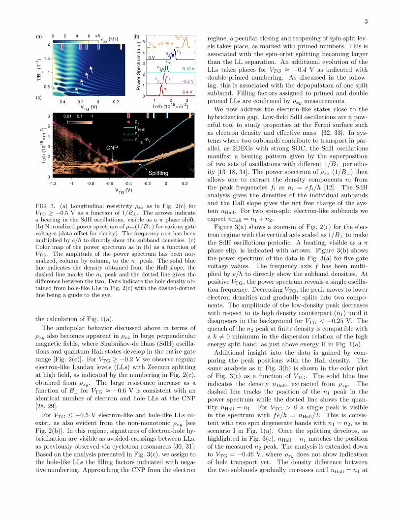
FIG. 3. (a) Longitudinal resistivity ρxx as in Fig. 2(c) forVTG ≥ −0.5 V as a function of 1/B⊥. The arrows indicatea beating in the SdH oscillations, visible as a π phase shift.(b) Normalized power spectrum of ρxx(1/B⊥) for various gatevoltages (data offset for clarity). The frequency axis has beenmultiplied by e/h to directly show the subband densities. (c)Color map of the power spectrum as in (b) as a function ofVTG. The amplitude of the power spectrum has been nor-malized, column by column, to the n1 peak. The solid blueline indicates the density obtained from the Hall slope, thedashed line marks the n1 peak and the dotted line gives thedifference between the two. Dots indicate the hole density ob-tained from hole-like LLs in Fig. 2(c) with the dashed-dottedline being a guide to the eye.
the calculation of Fig. 1(a).
The ambipolar behavior discussed above in terms ofρxy also becomes apparent in ρxx in large perpendicularmagnetic fields, where Shubnikov-de Haas (SdH) oscilla-tions and quantum Hall states develop in the entire gaterange [Fig. 2(c)]. For VTG ≥ −0.2 V we observe regularelectron-like Landau levels (LLs) with Zeeman splittingat high field, as indicated by the numbering in Fig. 2(c),obtained from ρxy. The large resistance increase as afunction of B⊥ for VTG ≈ −0.6 V is consistent with anidentical number of electron and hole LLs at the CNP[28, 29].
For VTG ≤ −0.5 V electron-like and hole-like LLs co-exist, as also evident from the non-monotonic ρxy [seeFig. 2(b)]. In this regime, signatures of electron-hole hy-bridization are visible as avoided-crossings between LLs,as previously observed via cyclotron resonances [30, 31].Based on the analysis presented in Fig. 3(c), we assign tothe hole-like LLs the filling factors indicated with nega-tive numbering. Approaching the CNP from the electron
regime, a peculiar closing and reopening of spin-split lev-els takes place, as marked with primed numbers. This isassociated with the spin-orbit splitting becoming largerthan the LL separation. An additional evolution of theLLs takes places for VTG ≈ −0.4 V as indicated withdouble-primed numbering. As discussed in the follow-ing, this is associated with the depopulation of one splitsubband. Filling factors assigned to primed and doubleprimed LLs are confirmed by ρxy measurements.
We now address the electron-like states close to thehybridization gap. Low-field SdH oscillations are a pow-erful tool to study properties at the Fermi surface suchas electron density and effective mass [32, 33]. In sys-tems where two subbands contribute to transport in par-allel, as 2DEGs with strong SOC, the SdH oscillationsmanifest a beating pattern given by the superpositionof two sets of oscillations with different 1/B⊥ periodic-ity [13–18, 34]. The power spectrum of ρxx (1/B⊥) thenallows one to extract the density components ni fromthe peak frequencies fi as ni = efi/h [12]. The SdHanalysis gives the densities of the individual subbandsand the Hall slope gives the net free charge of the sys-tem nHall. For two spin-split electron-like subbands weexpect nHall = n1 + n2.
Figure 3(a) shows a zoom-in of Fig. 2(c) for the elec-tron regime with the vertical axis scaled as 1/B⊥ to makethe SdH oscillations periodic. A beating, visible as a πphase slip, is indicated with arrows. Figure 3(b) showsthe power spectrum of the data in Fig. 3(a) for five gatevoltage values. The frequency axis f has been multi-plied by e/h to directly show the subband densities. Atpositive VTG, the power spectrum reveals a single oscilla-tion frequency. Decreasing VTG, the peak moves to lowerelectron densities and gradually splits into two compo-nents. The amplitude of the low-density peak decreaseswith respect to its high density counterpart (n1) until itdisappears in the background for VTG < −0.25 V. Thequench of the n2 peak at finite density is compatible witha k 6= 0 minimum in the dispersion relation of the highenergy split band, as just above energy II in Fig. 1(a).
Additional insight into the data is gained by com-paring the peak positions with the Hall density. Thesame analysis as in Fig. 3(b) is shown in the color plotof Fig. 3(c) as a function of VTG. The solid blue lineindicates the density nHall, extracted from ρxy. Thedashed line tracks the position of the n1 peak in thepower spectrum while the dotted line shows the quan-tity nHall − n1. For VTG > 0 a single peak is visiblein the spectrum with fe/h = nHall/2. This is consis-tent with two spin degenerate bands with n1 = n2, as inscenario I in Fig. 1(a). Once the splitting develops, ashighlighted in Fig. 3(c), nHall − n1 matches the positionof the measured n2 peak. The analysis is extended downto VTG = −0.46 V, where ρxy does not show indicationof hole transport yet. The density difference betweenthe two subbands gradually increases until nHall = n1 at
4
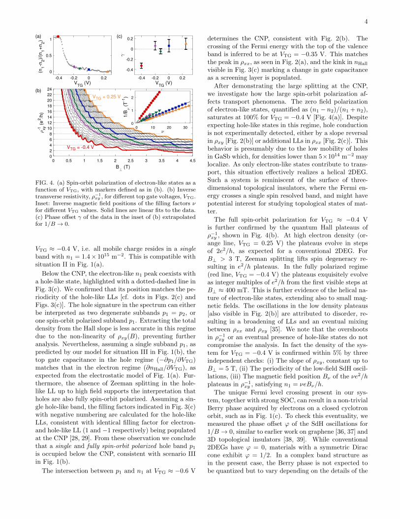
FIG. 4. (a) Spin-orbit polarization of electron-like states as afunction of VTG, with markers defined as in (b). (b) Inversetransverse resistivity, ρ−1
xy , for different top gate voltages, VTG.Inset: Inverse magnetic field positions of the filling factors νfor different VTG values. Solid lines are linear fits to the data.(c) Phase offset γ of the data in the inset of (b) extrapolatedfor 1/B → 0.
VTG ≈ −0.4 V, i.e. all mobile charge resides in a singleband with n1 = 1.4× 10¹⁵ m−2. This is compatible withsituation II in Fig. 1(a).
Below the CNP, the electron-like n1 peak coexists witha hole-like state, highlighted with a dotted-dashed line inFig. 3(c). We confirmed that its position matches the pe-riodicity of the hole-like LLs [cf. dots in Figs. 2(c) andFigs. 3(c)]. The hole signature in the spectrum can eitherbe interpreted as two degenerate subbands p1 = p2, orone spin-orbit polarized subband p1. Extracting the totaldensity from the Hall slope is less accurate in this regimedue to the non-linearity of ρxy(B), preventing furtheranalysis. Nevertheless, assuming a single subband p1, aspredicted by our model for situation III in Fig. 1(b), thetop gate capacitance in the hole regime (−∂p1/∂VTG)matches that in the electron regime (∂nHall/∂VTG), asexpected from the electrostatic model of Fig. 1(a). Fur-thermore, the absence of Zeeman splitting in the hole-like LL up to high field supports the interpretation thatholes are also fully spin-orbit polarized. Assuming a sin-gle hole-like band, the filling factors indicated in Fig. 3(c)with negative numbering are calculated for the hole-likeLLs, consistent with identical filling factor for electron-and hole-like LL (1 and −1 respectively) being populatedat the CNP [28, 29]. From these observation we concludethat a single and fully spin-orbit polarized hole band p1is occupied below the CNP, consistent with scenario IIIin Fig. 1(b).
The intersection between p1 and n1 at VTG ≈ −0.6 V
determines the CNP, consistent with Fig. 2(b). Thecrossing of the Fermi energy with the top of the valenceband is inferred to be at VTG = −0.35 V. This matchesthe peak in ρxx, as seen in Fig. 2(a), and the kink in nHall
visible in Fig. 3(c) marking a change in gate capacitanceas a screening layer is populated.
After demonstrating the large splitting at the CNP,we investigate how the large spin-orbit polarization af-fects transport phenomena. The zero field polarizationof electron-like states, quantified as (n1 − n2)/(n1 + n2),saturates at 100% for VTG = −0.4 V [Fig. 4(a)]. Despiteexpecting hole-like states in this regime, hole conductionis not experimentally detected, either by a slope reversalin ρxy [Fig. 2(b)] or additional LLs in ρxx [Fig. 2(c)]. Thisbehavior is presumably due to the low mobility of holesin GaSb which, for densities lower than 5×10¹⁴ m−2 maylocalize. As only electron-like states contribute to trans-port, this situation effectively realizes a helical 2DEG.Such a system is reminiscent of the surface of three-dimensional topological insulators, where the Fermi en-ergy crosses a single spin resolved band, and might havepotential interest for studying topological states of mat-ter.
The full spin-orbit polarization for VTG ≈ −0.4 Vis further confirmed by the quantum Hall plateaus ofρ−1xy , shown in Fig. 4(b). At high electron density (or-ange line, VTG = 0.25 V) the plateaus evolve in stepsof 2e2/h, as expected for a conventional 2DEG. ForB⊥ > 3 T, Zeeman splitting lifts spin degeneracy re-sulting in e2/h plateaus. In the fully polarized regime(red line, VTG = −0.4 V) the plateaus exquisitely evolveas integer multiples of e2/h from the first visible steps atB⊥ ≈ 400 mT. This is further evidence of the helical na-ture of electron-like states, extending also to small mag-netic fields. The oscillations in the low density plateaus[also visible in Fig. 2(b)] are attributed to disorder, re-sulting in a broadening of LLs and an eventual mixingbetween ρxx and ρxy [35]. We note that the overshootsin ρ−1xy or an eventual presence of hole-like states do notcompromise the analysis. In fact the density of the sys-tem for VTG = −0.4 V is confirmed within 5% by threeindependent checks: (i) The slope of ρxy, constant up toB⊥ = 5 T, (ii) The periodicity of the low-field SdH oscil-lations, (iii) The magnetic field position Bν of the νe2/hplateaus in ρ−1xy , satisfying n1 = νeBν/h.
The unique Fermi level crossing present in our sys-tem, together with strong SOC, can result in a non-trivialBerry phase acquired by electrons on a closed cyclotronorbit, such as in Fig. 1(c). To check this eventuality, wemeasured the phase offset ϕ of the SdH oscillations for1/B → 0, similar to earlier work on graphene [36, 37] and3D topological insulators [38, 39]. While conventional2DEGs have ϕ = 0, materials with a symmetric Diraccone exhibit ϕ = 1/2. In a complex band structure asin the present case, the Berry phase is not expected tobe quantized but to vary depending on the details of the
5
dispersion relation [40]. The inset of Figure 4(b) showsthe 1/Bν positions of the ν filling factors for various topgate voltages (markers) together with linear fits (lines)extrapolating to 1/B → 0. The result of the extrapola-tion is shown in Fig. 4(c). For VTG ≥ −0.2 V, all thecurves consistently give ϕ ≈ 0, as expected for normalfermions. For VTG = −0.4 V the extrapolation leads aphase shift ϕ = −0.33± 0.05, consistent with a non-zeroBerry phase.
In conclusion, we studied the band structure of in-verted InAs/GaSb QWs via magnetotransport measure-ments. Consistent with simulations, electron-like andhole-like states are fully spin-orbit polarized in proximityof the CNP. We identify a regime where a single electron-like band with helical spin texture contributes to trans-port. The 100% spin-orbit polarization of the systemis confirmed by quantum Hall plateaus evolving in e2/hsteps and a non-trivial Berry phase.
This work was supported from Microsoft Corpora-tion Station Q. The work in Copenhagen was also sup-ported from the Danish National Research Foundationand the Villum Foundation. The work in Delft was alsosupported by the Dutch Organisation for Scientific Re-search (NWO) and the Foundation for Fundamental Re-search on Matter (FOM). We thank Emmanuel Rashba,Joshua Folk and Karsten Flensberg for valuable discus-sions. F.N. acknowledges support of the European Com-mission through the Marie Curie Fellowship, grant agree-ment No 659653.
∗ email: [email protected][1] M. J. Yang, C. H. Yang, B. R. Bennett, and B. V.
Shanabrook, Phys. Rev. Lett. 78, 4613 (1997).[2] C. Liu, T. L. Hughes, X.-L. Qi, K. Wang, and S.-C.
Zhang, Phys. Rev. Lett. 100, 236601 (2008).[3] F. Qu, A. J. A. Beukman, S. Nadj-Perge, M. Wimmer,
B.-M. Nguyen, W. Yi, J. Thorp, M. Sokolich, A. A. Kise-lev, M. J. Manfra, C. M. Marcus, and L. P. Kouwen-hoven, Phys. Rev. Lett. 115, 036803 (2015).
[4] F. Nichele, H. J. Suominen, M. Kjaergaard, C. M. Mar-cus, E. Sajadi, J. A. Folk, F. Qu, A. J. A. Beukman, F. K.de Vries, J. van Veen, S. Nadj-Perge, L. P. Kouwenhoven,B.-M. Nguyen, A. A. Kiselev, W. Yi, M. Sokolich, M. J.Manfra, E. M. Spanton, and K. A. Moler, ArXiv e-prints(2015), arXiv:1511.01728 [cond-mat.mes-hall].
[5] I. Knez, R.-R. Du, and G. Sullivan, Phys. Rev. Lett.107, 136603 (2011).
[6] K. Suzuki, Y. Harada, K. Onomitsu, and K. Muraki,Phys. Rev. B 87, 235311 (2013).
[7] I. Knez, C. T. Rettner, S.-H. Yang, S. S. P. Parkin, L. Du,R.-R. Du, and G. Sullivan, Phys. Rev. Lett. 112, 026602(2014).
[8] L. Du, I. Knez, G. Sullivan, and R.-R. Du, Phys. Rev.Lett. 114, 096802 (2015).
[9] S. Mueller, A. N. Pal, M. Karalic, T. Tschirky, C. Char-pentier, W. Wegscheider, K. Ensslin, and T. Ihn, Phys.
Rev. B 92, 081303 (2015).[10] Zutic Igor, J. Fabian, and S. Das Sarma, Rev. Mod.
Phys. 76, 323 (2004).[11] We use the same subband definition as in Sec. 6.3.1 of
Ref. [12].[12] R. Winkler, Spin-Orbit Coupling Effects in Two-
Dimensional Electron and Hole Systems, Springer Tractsin Modern Physics, Vol. 191 (Springer-Verlag, Berlin,2003).
[13] J. Luo, H. Munekata, F. F. Fang, and P. J. Stiles, Phys.Rev. B 38, 10142 (1988).
[14] B. Das, D. C. Miller, S. Datta, R. Reifenberger, W. P.Hong, P. K. Bhattacharya, J. Singh, and M. Jaffe, Phys.Rev. B 39, 1411 (1989).
[15] J. P. Heida, B. J. van Wees, J. J. Kuipers, T. M. Klap-wijk, and G. Borghs, Phys. Rev. B 57, 11911 (1998).
[16] S. Brosig, K. Ensslin, R. J. Warburton, C. Nguyen,B. Brar, M. Thomas, and H. Kroemer, Phys. Rev. B60, R13989 (1999).
[17] Y. S. Gui, C. R. Becker, N. Dai, J. Liu, Z. J. Qiu, E. G.Novik, M. Schafer, X. Z. Shu, J. H. Chu, H. Buhmann,and L. W. Molenkamp, Phys. Rev. B 70, 115328 (2004).
[18] M. Nishioka, B. A. Gurney, E. E. Marinero, and F. Mire-les, Applied Physics Letters 95, 242108 (2009).
[19] H. L. Stormer, Z. Schlesinger, A. Chang, D. C. Tsui,A. C. Gossard, and W. Wiegmann, Phys. Rev. Lett. 51,126 (1983).
[20] B. Habib, E. Tutuc, S. Melinte, M. Shayegan, D. Wasser-man, S. A. Lyon, and R. Winkler, Phys. Rev. B 69,113311 (2004).
[21] F. Nichele, A. N. Pal, R. Winkler, C. Gerl, W. Wegschei-der, T. Ihn, and K. Ensslin, Phys. Rev. B 89, 081306(2014).
[22] G. M. Minkov, A. V. Germanenko, O. E. Rut, A. A. Sher-stobitov, S. A. Dvoretski, and N. N. Mikhailov, Phys.Rev. B 89, 165311 (2014).
[23] See Supplemental Material at [URL] for material andmethods and a description of the numerical simulations,which includes Refs. [41–53].
[24] A. Zakharova, S. T. Yen, and K. A. Chao, Phys. Rev. B66, 085312 (2002).
[25] J. Li, W. Yang, and K. Chang, Phys. Rev. B 80, 035303(2009).
[26] L.-H. Hu, C.-X. Liu, D.-H. Xu, F.-C. Zhang, andY. Zhou, ArXiv e-prints (2016), arXiv:1603.06074 [cond-mat.mes-hall].
[27] I. Knez, R. R. Du, and G. Sullivan, Phys. Rev. B 81,201301 (2010).
[28] R. J. Nicholas, K. Takashina, M. Lakrimi, B. Kardynal,S. Khym, N. J. Mason, D. M. Symons, D. K. Maude,and J. C. Portal, Phys. Rev. Lett. 85, 2364 (2000).
[29] F. Nichele, A. N. Pal, P. Pietsch, T. Ihn, K. Ensslin,C. Charpentier, and W. Wegscheider, Phys. Rev. Lett.112, 036802 (2014).
[30] S.-F. Tsay, J.-C. Chiang, Z. M. Chau, and I. Lo, Phys.Rev. B 56, 13242 (1997).
[31] Y. Vasilyev, S. Suchalkin, K. von Klitzing, B. Meltser,S. Ivanov, and P. Kopev, Phys. Rev. B 60, 10636 (1999).
[32] T. Ando, A. B. Fowler, and F. Stern, Rev. Mod. Phys.54, 437 (1982).
[33] P. T. Coleridge, R. Stoner, and R. Fletcher, Phys. Rev.B 39, 1120 (1989).
[34] Y. A. Bychkov and E. I. Rashba, Journal of Physics C:Solid State Physics 17, 6039 (1984).
6
[35] B. Huckestein, Rev. Mod. Phys. 67, 357 (1995).[36] K. S. Novoselov, A. K. Geim, S. V. Morozov, D. Jiang,
M. I. Katsnelson, I. V. Grigorieva, S. V. Dubonos, andA. A. Firsov, Nature 438, 197 (2005).
[37] Y. Zhang, Y.-W. Tan, H. L. Stormer, and P. Kim, Nature438, 201 (2005).
[38] D.-X. Qu, Y. S. Hor, J. Xiong, R. J. Cava, and N. P.Ong, Science 329, 821 (2010).
[39] J. Xiong, Y. Luo, Y. Khoo, S. Jia, R. J. Cava, and N. P.Ong, Phys. Rev. B 86, 045314 (2012).
[40] A. R. Wright and R. H. McKenzie, Phys. Rev. B 87,085411 (2013).
[41] B.-M. Nguyen, W. Yi, R. Noah, J. Thorp, andM. Sokolich, Applied Physics Letters 106, 032107 (2015).
[42] J. Tukey, Advance Seminar on Spectral analysis of timeseries: proceedings (Wiley, 1967) pp. 25–46.
[43] F. Harris, Proceedings of the IEEE, Proc. IEEE 66, 51(1978).
[44] S. Luryi, Appl. Phys. Lett. 52, 501 (Luryi1988).[45] E. O. Kane, in Handbook on Semiconductors, Vol. 1,
edited by W. Paul (North-Holland, Amsterdam, 1982)p. 193.
[46] G. Bastard, Wave Mechanics Applied to SemiconductorHeterostructures (Wiley, New York, 1988).
[47] M. G. Burt, J. Phys.: Condens. Matter 4, 6651 (1992).[48] B. A. Foreman, Phys. Rev. B 56, R12748 (1997).[49] E. G. Novik, A. Pfeuffer-Jeschke, T. Jungwirth, V. La-
tussek, C. R. Becker, G. Landwehr, H. Buhmann, andL. W. Molenkamp, Phys. Rev. B 72, 035321 (2005).
[50] A. J. Pfeuffer-Jeschke, Transport experiments in two-dimensional systems with strong spin-orbit interac-tion, Ph.D. thesis, Physikalisches Institut, UniversitatWurzburg (2000).
[51] E. Halvorsen, Y. Galperin, and K. A. Chao, Phys. Rev.B 61, 16743 (2000).
[52] P. Lawaetz, Phys. Rev. B 4, 3460 (1971).[53] T. Andlauer and P. Vogl, Phys. Rev. B 80, 035304 (2009).
SUPPLEMENTAL MATERIAL
This Supplemental Material Section describes thewafer structure, the sample fabrication procedure andthe measuring setup. We describe the numerical pro-cedure used to Fourier transform the magnetoresistanceand derive the subbands density. We further describe theelectrostatic model used to calculate electron and holedensities as a function of top gate voltage and the k · psimulations for band structure calculations.
Material and Methods
The wafer structure was grown by molecular beam epi-taxy on a [001] oriented GaSb substrate. From top tobottom it consists of a 3 nm GaSb capping layer, a 50 nmAlSb insulating barrier, a 5 nm GaSb QW grown on topof a 12.5 nm InAs QW, a second AlSb barrier and a thickGaSb buffer layer. More information on wafer growth arereported in Ref. 3, 4, and 41.
A 100 × 50 µm2 Hall bar structure was patternedwith conventional electron beam lithography techniquesand wet etching. The Hall bar structure was orientedalong the [110] crystallographic direction. For wet etch-ing we used a general III-V etching solution consist-ing of H2O : C6H8O7 : H3PO4 : H2O2 in concentration220 : 55 : 3 : 3. The solution was kept at room tem-perature and well stirred, resulting in an etching rate ofapproximately 1 nm s−1. Ohmic contacts were definedby etching the wafer down to the InAs quantum well anddepositing Ti/Au electrodes, without any annealing. Thesample was covered with a 40 nm HfO2 insulating layergrown by atomic layer deposition and a global Ti/Au topgate.
Transport measurements were performed in a dilutionrefrigerator with a base temperature of 50 mK using lowfrequency (< 100 Hz) lock-in techniques. The ampli-tude of the AC currents was always kept small enough(≤ 20 nA) to prevent sample heating. Due to the onsetof leakage currents at finite bias, the device was operatedat zero back gate voltage, where the resistance betweenthe 2DEG and the back gate was in excess of 10 GΩ.
Fourier transforming techniques
We now describe the numerical procedure used toFourier transform the Shubnikov-de Haas (SdH) oscil-lations in the longitudinal resistivity ρxx. The magneticfield range for the analysis was chosen, case by case, toinclude only SdH oscillations whose amplitude was smallcompared to the zero field ρxx. We first plotted the quan-tity ρxx(1/B), where the oscillations are periodic. Thecurve was interpolated on a new 1/B axis with constantspacing between points. At this point, we removed the

7
slowly varying background of the data by subtracting thefit to a low order polynomial. In order to improve thefinal output of the Fourier transform, we adopted stan-dard numerical procedures [42] such as padding the datawith zeros and windowing [43]. In case of a 2DEG withstrong spin-orbit coupling (SOC), the frequency axis fis converted into density via ni = efi/h. In a conven-tional two-dimensional electron gas, an additional factorof two would be necessary to convert frequency into den-sities: ni = 2efi/h. The same analysis is described withgreater details in Ref. 21. We note that the position ofthe power spectrum peaks of Fig. 3 of the main text wasaffected by less than 5% by modifying the details of thisanalysis. The final result of this procedure still containsspurious low frequency components, which originate fromthe difficulties in completely removing the slowly varyingbackground of the original data. To suppress such fea-tures we multiplied the spectra by a high pass filter withcut-off frequency ef/h = 0.4× 10¹⁵. Finally, the spectrawere normalized, for each value of VTG, to the amplitudeof the n1 peak.
The Fourier transform analysis presented in the maintext for VTG ≥ −0.46V is fully compatible with two spin-orbit split subbands. In fact the relation n1 +n2 = nHall
is always satisfied, where nHall is independently obtainedfrom ρxy. In case of orbital electron-like subbands, anadditional factor of two would be necessary for convertingthe power spectrum frequencies to densities, to includespin degeneracy.
Additional Data
Charge Neutrality Point
Figure S.1 shows in more detail the longitudinal re-sistivity ρxx and the transverse resistivity ρxy (red andblue respectively) measured at VTG = −0.59 V, iden-tified as the zero field CNP. The lack of a net slope inρxy is indicative of equal electron and hole concentration.The presence of oscillations in ρxx confirms the dominantcontribution of bulk transport at the CNP, as predictedby band structure calculations for negative gate voltages[cfg. Fig. S.4(a)].
Spin-Orbit Splitting in the Electron Regime
For better clarity, we reproduce here the longitudinalresistivity data measured in the electron regime withoutany overlay. Figure S.2(a) shows the longitudinal resis-tivity ρxx in the gate range where no indication of holetransport is detected. The same data is shown again inFig. S.2(b) plotted as a function of 1/B⊥, that makesthe oscillations quasi-periodic along the vertical axis. Fi-nally, Fig. S.2(c) shows the power spectrum of the data in
FIG. S.1. Longitudinal (red) and transverse (blue) resistivi-ties measured at the zero-field CNP.
Fig. S.2(b) in arbitrary units and linear scale. From thepower spectrum we observe a splitting of the main peak,coincidental with the development of a beating patternin ρxx(1/B⊥). As the lower density split peak moves tolower density, its amplitude decreases.
Numerical simulations
Capacitor model
To estimate the electric fields in the quantum wellwe use the capacitor model introduced in Ref. 3 (seeFig. S.3(a). With the material parameters from Ref. 3and assuming the dielectric constant of HfO2 as εHfO2
=25 we find the geometric capacitances for our quantumwell structure as CT = 135 nF/cm2, CM = 1.6µF/cm2,and CB = 177 nF/cm2. The quantities Ce and Ch arequantum capacitances [44] that are non-zero only if thereis a finite carrier density. The capacitor model neglectsthe intrinsic inversion of electron and hole bands in theInAs/GaSb quantum well, but assumes that the Fermienergy is aligned with the electron and hole band bot-tom when the potential in the respective layer is 0 V.Hence, Ce = 2.7µF/cm2 if Ve > 0 and zero else, whereasCe = 6µF/cm2 if Vh < 0 and zero else. Ve and Vh arethe potential values in the middle of the InAs and GaSblayers.
In our experiments, the back gate is always kept atVBG = 0 V. The assumptions of the capacitor modelthen imply that for VTG = 0 V both electron and holedensity are zero. In the experiment, we however find anonzero electron density in this case, due to in-built elec-tric fields. We approximate these electric fields by a finitefictitious back gate voltage VBG that we fix such that werecover the experimentally measured electron density ofn ≈ 4.5× 10¹⁵m−2 for VTG = 0 V (see Fig. 3 in the maintext).
Even with its simplifications, the capacitor model cap-tures essential features of the experiment: Fig. S.3(b)shows electron and hole densities as a function of topgate voltage. Equal densities of electrons and holes are

8
FIG. S.2. Same data presented in the main text, but focusedon the electron regime. (a) Longitudinal resistivity ρxx. (b)As in (a) but as a function of inverse out-of-plane magneticfield B⊥. (c) Power spectrum of the data in (b). The am-plitude has been normalized, column by column, to the n1
peak. Differently from Fig. 3(c) of the main text, we plot theamplitude in linear scale.
FIG. S.3. (a) Schematic of the capacitor model for InAs/GaSbquantum wells. (b) Electron (n) and hole (p) densities ob-tained from the capacitor model as a function of the top-gatevoltage VTG
found around VTG = −0.6 V which agrees with the volt-age where the charge neutrality point is found experimen-tally. Additionally, we observe that the gate-tunabilityof the electron density is strongly reduced when holesare occupied. The finite density of charge carriers in theGaSb (hole) layer lieing between top gate and (electron)InAs layer screens the electric field. A similar feature isseen in Fig. 3 of the main text. The screening by thehole layer also explains why experimentally the secondelectron Fermi surface is never recovered within our gatevoltage range.
We note that the capacitor model assumes constantdensity of states of the electron and hole layer, and noelectron-hole mixing. For this reason, the quantitativeresults of Fig. S.3 are valid in the high density limit, butshould be taken with care close to the CNP, where thedensity of states shows gaps and singularities.
k.p simulations
The numerical band structure simulations use the stan-dard semiconductor k · p model [45, 46]. The 8 × 8Kane Hamiltonian contains position-dependent parame-ters corresponding to the different material layers, andmust be properly symmetrized. Following the sym-metrization put forward by Burt and Foreman[47, 48],the Hamiltonian for the [001] growth direction takes thefollowing form:[49, 50]
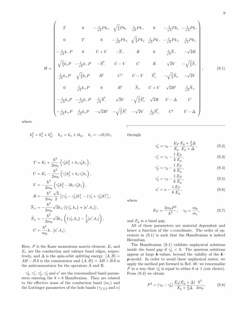
9
H =
T 0 − 1√2Pk+
√23Pkz
1√6Pk− 0 − 1√
3Pkz − 1√
3Pk−
0 T 0 − 1√6Pk+
√23Pkz
1√2Pk− − 1√
3Pk+
1√3Pkz
− 1√2k−P 0 U + V −S− R 0 1√
2S− −
√2R√
23kzP − 1√
6k−P −S†− U − V C R
√2V −
√32 S−
1√6k+P
√23kzP R† C† U − V S
†+ −
√32 S+ −
√2V
0 1√2k+P 0 R† S+ U + V
√2R† 1√
2S+
− 1√3kzP − 1√
3k−P
1√2S†−
√2V −
√32 S†+
√2R U −∆ C
− 1√3k+P
1√3kzP −
√2R† −
√32 S†− −
√2V 1√
2S†+ C† U −∆
, (S.1)
where
k2‖ = k2x + k2y, k± = kx ± iky, kz = −i∂/∂z,
T = Ec +h2
2m0
(γ′0k
2‖ + kzγ
′0kz
),
U = Ev −h2
2m0
(γ′1k
2‖ + kzγ
′1kz
),
V = − h2
2m0
(γ′2k
2‖ − 2kzγ
′2kz
),
R = − h2
2m0
√3
2
[(γ′3 − γ′2)k2+ − (γ′3 + γ′2)k2−
],
S± = − h2
2m0
√3k± (γ′3, kz+ [κ′, kz]) ,
S± = − h2
2m0
√3k±
(γ′3, kz −
1
3[κ′, kz]
),
C =h2
m0k− [κ′, kz] .
Here, P is the Kane momentum matrix element, Ec andEv are the conduction and valence band edges, respec-tively, and ∆ is the spin-orbit splitting energy. [A,B] =AB −BA is the commutator and A,B = AB +BA isthe anticommutator for the operators A and B.
γ′0, γ′1, γ′2, γ′3 and κ′ are the renormalized band param-eters entering the 8 × 8 Hamiltonian. They are relatedto the effective mass of the conduction band (mc) andthe Luttinger parameters of the hole bands (γ1,2,3 and κ)
through
γ′0 = γ0 −EPEg
Eg + 23∆
Eg + ∆, (S.2)
γ′1 = γ1 −1
3
EPEg
, (S.3)
γ′2 = γ2 −1
6
EPEg
, (S.4)
γ′3 = γ3 −1
6
EPEg
, (S.5)
κ′ = κ− 1
6
EPEg
, (S.6)
where
EP =2m0P
2
h2, γ0 =
m0
mc, (S.7)
and Eg is a band gap.All of these parameters are material dependent and
hence a function of the z-coordinate. The order of op-erators in (S.1) is such that the Hamiltonian is indeedHermitian.
The Hamiltonian (S.1) exhibits unphysical solutionsinside the band gap if γ′0 < 0. The spurious solutionsappear at large k-values, beyond the validity of the k ·p-model. In order to avoid these unphysical states, weapply the method put forward in Ref. 48: we renormalizeP in a way that γ′0 is equal to either 0 or 1 (our choice).From (S.2) we obtain
P 2 = (γ0 − γ′0)Eg(Eg + ∆)
Eg + 23∆
h2
2m0, (S.8)
10
which we then use to modify the Luttinger parametersusing (S.3-S.6). This method pushes unphysical solutionsat large k out of interesting energies, whilst preservingthe band structure around k = 0.
For our simulations, we take the band structure param-eters from [51, 52] (summarized in Table I). The valenceband offsets [51] are 0.56 eV for GaSb-InAs, 0.18 eV forAlSb-InAs and −0.38 eV for AlSb-GaSb.
Gate dependence of the band structure
Computing the gate dependence of the band structureof InAs/GaSb quantum wells quantitatively requires aself-consistent solution of the 8 × 8 Kane Hamiltonianand the Poisson equation. This problem involves bothelectron and hole densities, and while some approximateapproaches have been discussed [53], it has not yet beensolved satisfactorily. For this reason we choose to onlytake into account the electrostatics due to gating on thelevel of the capacitor model. We extract a electrostaticpotential V (z), approximating the voltage drop betweenthe nodes of the capacitor model as linear (this is justi-fied as the dielectric constants of the different materialsdiffer by at most a factor of 2). This potential enters theKane Hamiltonian (S.1) as an additional term on the di-agonal. Finally, the spin texture shown in Fig. 1(c) of themain text are calculated as the expectation value of theelectron spin Pauli matrices σx,y at a constant energy.
The use of the capacitor model is justified in that weonly strive to capture the qualitative aspects of the bandstructure. Further, as we see below, the spin-orbit fea-tures depend little on gating, as they are dominated bythe intrinsic inversion symmetry breaking in the quan-tum well structure.
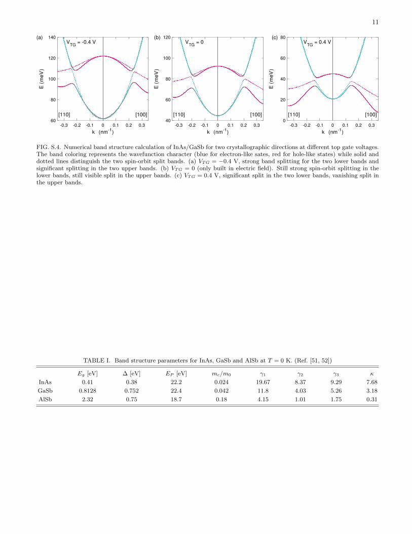
We present result of the band structure calculation fordifferent top gate voltage in Fig. S.4. We show resultsfor the [110] crystallographic direction on the left handside of each plot, and results for the [100] direction ofthe right hand side. The colors of the band indicate thewavefunction character (blue for electron-like and red forhole-like states) while solid and dashed lines distinguishthe two spin-orbit split bands. We describe the proceudeused to calculate the colors in Sec. . The biggest effect ofthe gate voltage is an change of the k = 0 gap betweenthe hole and the electron bands due to the electric field.As a consequence, the hybridization gap occurs at largermomenta for more negative top-gate voltages. At thesame time, the hybridization gap becomes smaller andeventually vanishes. This is consistent with the experi-ment that finds still a significant residual conductance atthe charge neutrality point.
The spin splitting in the band above the hybridiza-tion gap is gate-voltage dependent (from well visible atVTG = −0.4 V) to nearly vanishing at VTG = 0.4 V)).On the other hand, the large spin-orbit splitting in thebands below the hybridization gap is largely indepen-dent of gate voltage. Therefore at every gate voltagewe can choose a Fermi level that corresponds to a sys-tem characterized by a single electron spin species. Thehybridization gap also changes with gate voltage. For ex-ample a large positive gap is obtained for VTG = 0.4 V).In that situation, and with the Fermi energy placed inthe gap with the help of a back gate voltage, the systemwould reach the topological insulator regime. As the topgate voltage is made more negative, the bands overlapincreases and the hybridization gap reduces. In particu-lar, already at VTG = −0.4 V close inspection reveals thegap is anisotropic and vanishes along the [110] direction.As a result, at the energy level II of Fig. 1(b) of the maintext, four Fermi pockets centered along the [110] direc-tion could be present. In the present work we believedisorder potential could largely smear these features, ifactually present in our samples. Furthermore their largeeffective mass would make negligible their contributionin transport. For this reason their presence is ignored inthe left hand side of Fig. 1(c) of the main text.
Estimation of electron-hole mixing in momentumstates
The wave functions of momentum states that wepresent in Fig. 1(b) of the main text and in Fig. S.4 con-tain both electron and hole components. Assuming theorder of different wave function components is in agree-ment with the Hamiltonian of Eq. S.1, we define
|ψe|2 =
n=2∑n=1
∫|ψn(x)|2 dx; (S.9)
|ψh|2 =
n=8∑n=3
∫|ψn(x)|2 dx, (S.10)
where
|ψe|2 + |ψh|2 = 1. (S.11)
The blue color on the band structure plots correspondsto pure electron state ,|ψe|2 = 1, and the pink color cor-responds to pure hole state, |ψh|2 = 1. The smooth colorvariation from blue to red indicates the mixing of electronand holes states along the energy bands.
11
FIG. S.4. Numerical band structure calculation of InAs/GaSb for two crystallographic directions at different top gate voltages.The band coloring represents the wavefunction character (blue for electron-like sates, red for hole-like states) while solid anddotted lines distinguish the two spin-orbit split bands. (a) VTG = −0.4 V, strong band splitting for the two lower bands andsignificant splitting in the two upper bands. (b) VTG = 0 (only built in electric field). Still strong spin-orbit splitting in thelower bands, still visible split in the upper bands. (c) VTG = 0.4 V, significant split in the two lower bands, vanishing split inthe upper bands.
TABLE I. Band structure parameters for InAs, GaSb and AlSb at T = 0 K. (Ref. [51, 52])
Eg [eV] ∆ [eV] EP [eV] mc/m0 γ1 γ2 γ3 κ
InAs 0.41 0.38 22.2 0.024 19.67 8.37 9.29 7.68
GaSb 0.8128 0.752 22.4 0.042 11.8 4.03 5.26 3.18
AlSb 2.32 0.75 18.7 0.18 4.15 1.01 1.75 0.31