Embed Size (px)
Citation preview
G.H.RAISONI COLLEGE OF ENGINEERING,NAGPUR Department:-Electronics & Communication Engineering
Branch:-5thSemester[Electronics] Subject:- Power Electronics
List of Experiments
CYCLE :- 1 1. To study and plot V-I characteristics of SCR.
2. To study and plot MOSFET characteristics.
3. To study and plot V-I characteristics of TRIAC.
4. To study UJT as Relaxation Oscillator.
5. To study and plot IGBT characteristics.
CYCLE: - 2
6. To study series inverter.
7. To study parallel inverter.
8. To study different types of commutations.
9. To study and plot characteristics of DC chopper.
10. To study and plot the characteristics of single-phase converter.
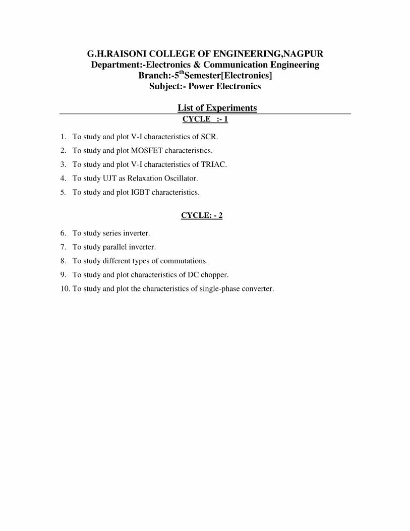
Experiment No: -1 Aim: - To study and plot the characteristics of SCR Apparatus: - SCR Kit
Voltmeter (0-50V) Ammeter (0-50mA) Ammeter (0-500mA),
Patch Chord Theory: - SCR is a four-layered PNPN switching device having three junctions and three terminals known as Anode, Cathode and Gate terminals. When the end P-layer is made positive with respect to the end N-layer, the two outer junctions J1 & J3 are forward biased but the middle layer is reversed biased. Thus the junction J2 because of the presence of depletion layer does not allow any current to flow through the device. Only leakage current negligibly small in magnitude flows through the device due to the drift of the mobile charges. This current is insufficient to make the device conduct. The depletion layer mostly of immobile charges does not conduct. This is called forward blocking state of the device.
On reverse biased conduction, J1 & J3 are reverse biased while J2 is forward biased. The junction J1 & J3 do not allow any current to flow through the device. Only very small leakage current flows through the device. This is known as reverse blocking state or off state of the device. Circuit Diagram: -

Observation Table: -
VAK IA
Procedure: - 1) Study the circuit given on front panel of kit. 2) Connect milliammeter & voltmeter in the circuit 3) Connect dc power supply in gate & A to K circuit. 4) Keeping gate current constant increase VAK in steps to note anode- cathode current IAK , for each step till SCR fires 5) Note the value of IH by gradually decreasing the voltage VAK
6) Plot SCR characteristics between IAK & VAK . Result: - Characteristics of SCR were studied & found that SCR turned on when IA > IL & Remained in on state until IA > IH Viva question: -
1. What is latching current in SCR. 2. What is holding current in SCR. 3. What is forward break over voltage.
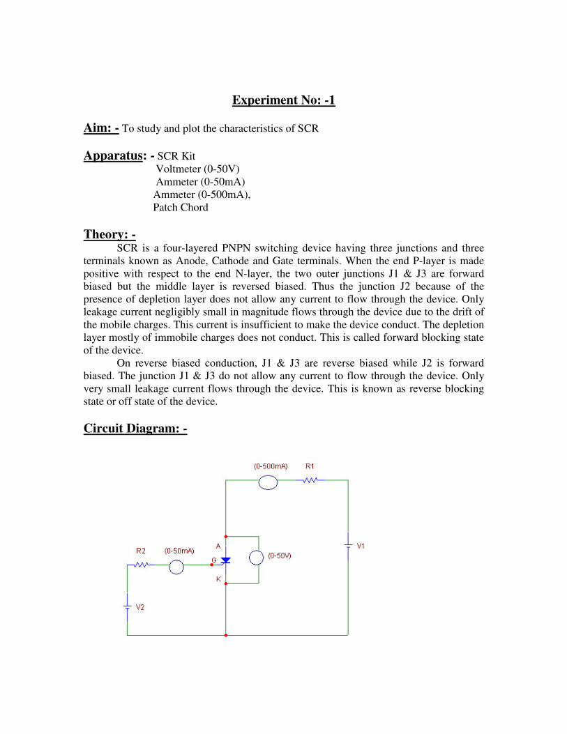
Experiment No: -2
Aim: - To study and plot the characteristics of MOSFET Apparatus: - MOSFET Kit, Voltmeter (0-50V)
Ammeter (0-50mA) Patch Chord
Ammeter (0- 500mA) Voltmeter (0-50V)
Theory: - MOSFET is an abbreviation for metal oxide semiconductor filed transistor. Like JFET, it has a source (S), drain(D) and gate(G). However unlike JFET, the gate of MOSFET is insulated from channel. Because of this, MOSFET is sometimes known as IGFET (insulated gate FET). Basically MOSFET are of two types 1) depletion type MOSFET and 2) enhancement type MOSFET. Enhancement MOSFET has no depletion mode and only operates in enhancement mode. It differs in construction from depletion type MOSFET in the sense that it has no physical channel. The min gate-source voltage (VGS), which produces inversion layer, called as threshold voltage. Drain characteristics for enhancement MOSFET: - When VGS< (VGS) the no drain current flows. However in actual practice, and extremely small value of drain current does flow through MOSFET. This current flow is generally due to presence of thermally generated electron in P type substrate when value of VGS is kept above (VGS) significant drain current flow. Transfer characteristics of MOSFET: - When VGS=0 there is no drain current, however if VGS is increased rapidly as shown in fig. The relation gives the drain current at any instant along the curve. ID=k [(VGS-VGS)] Circuit Diagram: -

Observation Table: -
VDS ID
Procedure: - 1) Keep VDS say 5 V & vary VGS in steps & note down corresponding value of drain current. 2) When keeping VGS at VGS & vary VDS in steps to note corresponding value of drain current. 3) Then repeat for different values of constant VGS & constant VDS. 4) Plot the drain characteristics VDS , VS ID for constant value of VGS & plot the graph for transfer characteristics where VGS VS ID is plotted keeping VDS constant Result: - The transfer & drain characteristics of power MOSFET has been plotted & Studied. Viva question: - 1) Explain transfer characteristics of power MOSFET? 2) Explain enhancement type MOSFET?
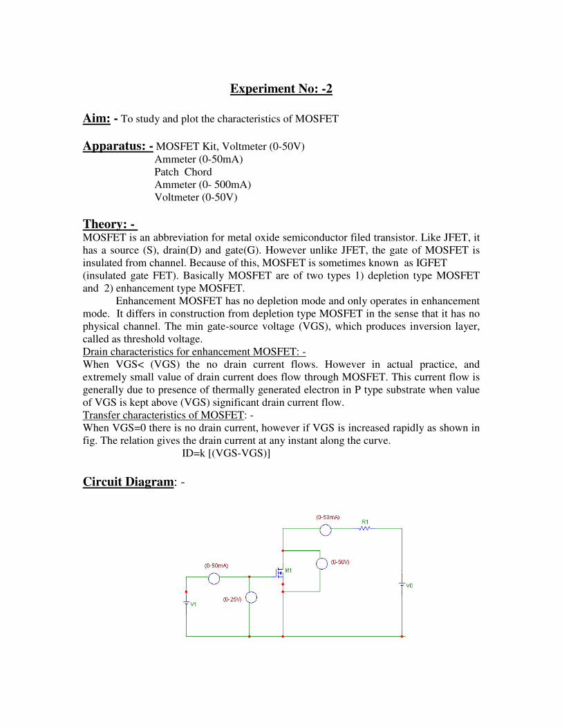
Experiment No: – 3 Aim: - To study TRIAC characteristics. Apparatus: - Experimental kit
Patch chord Voltmeter (0-50v) Ammeter (0-25mA) Ammeter (0-500mA) Multimeter.
Theory: - TRIAC is three terminal bi-directional high power device. Conduction takes place in both directions i.e. from MT1 to MT2 or MT2 to MT1. Gate terminal is towards MT1 in operation TRAIC is equivalent to two SCR’s connected in anti parallel. The layer diagram symbolic representation of TRAIC is as shown VI characteristic of SCR and TRAIC are similar. The only difference is that VI characteristics is symmetrical in TRAIC. TRAIC can be run on in four modes I+ Mode: - In this mode MT2 is positive with respect to MT1 and gate is made positive w.r.t. MT1. I- Mode: - In this mode MT2 is positive with respect to MT1 and gate is made negative w.r.t. MT1. III+ Mode: - In this mode MT2 is negative with respect to MT1 and gate is made positive w.r.t. MT1. III- Mode: - In this mode MT2 is negative with respect to MT1 and gate is made negative w.r.t. MT1. Circuit diagram: -

Observation Table: - Forward characteristics – IG ( CONSTANT) = 4 , 8 . Sr. no. VAK IAK
Reverse characteristics – IG ( CONSTANT) = 15 , 16 . Sr. no. VAK IAK
Procedure :-
1) Connect the circuit as shown in circuit diagram . 2) Make the connections for I + mode . 3) Keep the IG constant and note down the voltmeter and ammeter reading . 4) Now make the connections in III - mode . 5) Keep IG constant and note down the voltmeter and ammeter reading . 6) Plot the graph for both the characteristics.
Results :- Characteristics of TRIAC were studied and plot the graph from the reading. Viva Question:-
1) What are the applications of TRIAC? 2) Why TRIAC is known to be bi-directional devices?
Experiment No:-4 Aim: -To study UJT as relaxation oscillator. Apparatus :-Ammeter(0-5 m A), UJT KIT , patch chords, voltmeter(0-30 V). Theory :-
An UJT is made up of an N-type silicon bar to which P-type emitter is embedded .It has three terminals namely emitter E, base B1 & B2 .Between bases B1 & B2 UJT behave like an ordinary resistance RB1 & RB2 are the internal resistances respectively from base B1 & B2 to ETA point A.
When voltage VBB is applied across the two base terminals B1 & B2 .The potential of point A w.r.t B1 is given by : VAB1= VBB* RB1/RB1+RB2=ηVBB
Where η is called as intrinsic stand off ratio critically value of η is from 0.52 to 0.82.Internal resistance RB1 + RB2 =RBB is of order of 5 to 10 kΩ .
When a voltage is applied between emitter E and base B1 .So that E is positive w.r.t B1. This voltage is increased from zero as long as the emitter voltage VE is less than ηVBB. The emitter base B1 junction is reverse biased and emitter current IE is negative .
When emitter voltage VE is equal to ηVBB +VD at point B1 , IE is positive and emitter and emitter to base junction begins to conduct here ,VD is forward voltage drop from emitter to base junction.
Point B is called the peak point and corresponding emitter voltage and VP and IP denote current. At point B when VE=ηVBB+VD, the emitter starts to inject holes into the lower base region B1 because of increase no. of holes in base region resistance RB1 of emitter base B1 junction decreases as a result potential of ETA point A pulls and therefore current IC due to voltage VC increase s .At point C entire base region is saturated and resistance RB1 does not decreases further. A further increases in IE
accompanied by rise in voltage VE ,this curve is given by CD point C is called valley point .
The negative resistance between peak and valley point use the UJT switching characteristics for the use in SCR triggering .
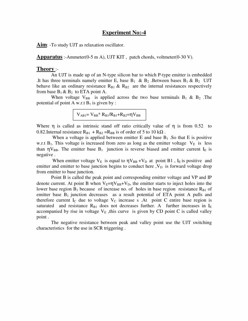
Circuit diagram:- Observation Table:-
Sr. No. IE(m A) VE(V) 1. 2.
Procedure :- 1) Make connections as shown in fig. 2) Fix the voltage EBB at 0 volt and vary VE. 3) Note down the current and voltage . 4) Plot the V-I characteristics as shown in fig . 5) Repeat the above procedure by keeping voltage Ebb at 5,10,15,20v. Result :- The V-I characteristics of UJT has been studied and plotted on graph successfully. Viva Question:- 1) What do you mean by intrinsic stand off ratio? 2) What do you mean by negative resistance region?
VEE
VBB IE
VE
IB
RB2
RB1
RE
UJT
RB
Experiment No: –5 Aim:- Study characteristics of IGBT. Apparatus :-Experimental kit
Voltmeter (0-50v) Ammeter (0-25mA) Ammeter (0-500mA) Patch chord.
Theory:-
An IGBT Insulated Gate Bipolar Transistor combines advantages of both BJT and MOSFET. An IGBT have high input impedance like MOSFET and low on state conduction loses like BJT.
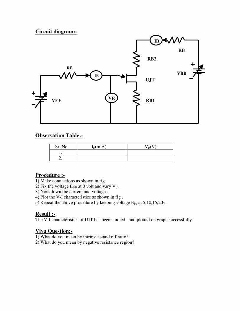
It has three terminals namely Gate , Collector and Emitter instead of Gate , Drain and Source as in MOSFET. The parameters and their symbols are similar to that of MOSFET except that the subscript D and S have been changed. The current rating of single IGBT can be up to 400A, 1200V and switching frequency can be up to 20KHz. An IGBT is inherently faster than a BJT. The structure of IGBT is quite similar to MOSFET. The IGBT conducts in two modes reverse blocking mode and forward blocking mode. If gate – emitter voltage applied is of sufficient magnitude to surface the base region under gate, device switches to its positive forward conduction state and current can flow from collector N-region to base N- region. Circuit Diagram:-

Observation Table:- VCE = 5v(const..) Sr.no VGE ICE
VGE = 5v(const..) Sr.no VCE ICB
Procedure :-
1. Make connections as shown in circuit diagram. 2. Apply same positive collector to emitter voltage keeping collector at higher
potential with gate. 3. Apply gate to emitter voltage at VGE and base different values of I CE for constant
value VCE . 4. Plot graph of VGE VS I CE for constant value of V CE . 5. For dynamic characteristics , apply suitable gate to emitter voltage keeping its
constant VGE and examining the readings VCE and I CE . 6. Plot graph of VCE vs I CE .
Result :- I/p &o/p characteristics of IGBT can be studied. Viva Questions:-
1) Draw the characteristics of IGBT. 2) Draw the layered diagram of IGBT.

Experiment No:-06
Aim: - To study series inverter. Apparatus: - CRO dual channel multimeter, patch cords CRO probes etc
Theory: -
Fig shows the schematic diagram of modified series inverter. Here inductor L1 and L2 are identifies and coupled capacitor C1 and C2 are also identical.
Let the initial voltage across capacitor C2 be EC, with the polarity as shown lower plate positive. Then capacitor C1 will be charged to voltage (VDC+Ec) in the opposite direction. When SCR1 is fired, then will be tow parallel paths for load current i2 current i1 will flow from the positive DC terminal through SCR1-L1-load-capacitor C2 to the negative terminal of supply current i2 will flow from C1, through SCR1-L1-Load. The driving voltage (VDC+Ec) the circuit elements. The initial condition is identical for both those paths. Therefore the two current s will be equal hence one half of the load current will come from the DC supply and other half form the discharge of the capacitor at the end of the half cycle. When the load current becomes zero, SCR1 will be turn off and the voltage across the capacitor reversed.
In the steady state capacitor C2 will be charged to voltage (VDC+Ec) in the opposite direction and capacitor C1 To E2. Identical operation will take place in the following negative half cycle whenSCR2 is triggered. Then one half of the load current will supply form the input and other half from the discharge of capacitor C2.
Circuit diagram:-

Procedure: -
1. Connect the circuit as shown in figure. 2. Make the connection with the help of patch cords on series inverter experimental
kit. 3. Give DC input to the series inverter. 4. Observe the waveforms on dual channel CRO by connecting on output of series
inverter to the CRO. 5. The output of series inverter is AC, is noted carefully. 6. Measure the output F and A.
Result:- Modified series inverter has been studied successfully. Viva Questions:- 1) What are the advantages of basic series inverter? 2) Compare basic &modified series inverter?
Experiment No:-07 Aim: - To study the circuit of parallel inverter.
Apparatus: - Experimental kit
Dual channel COR Patch chords Ammeter (0-5A) Voltmeter (0-50V)
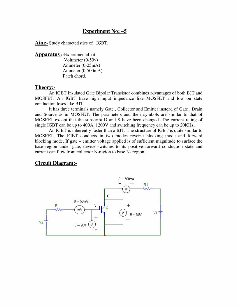
Components: - Thyrister T1 and T2 Inductor L Diodes D1 and D2.
Theory: -
The process of converting DC into AC is known as inverting. In other words we can define it as reverse process of rectification .the device, which performs this process, is called as inverter.
The basic principle of inverter can be explained with the help of simple circuit shown in figure. Here we have used SCR for switching due to high current of the circuit according to the connection of thyrister and commutating components the device may be classified into three groups.
All the basic commutation components are L & C. The capacitor is connected in parallel with the load therefore it is called as parallel inverter.
The parallel inverter consists of two feedback diodes D1 & D2. the function of these feedback diode is that they feedbacks the reactive power i.e. the energy stored by the commutation capacitor C,L and load induction back to DC supply.
Circuit Diagram:-

Procedure: - 1) Study the circuit given on the front panel of the kit. 2) Switch on the power supply note down the DC supply. 3) Connect the CRO to the kit and observe waveforms on CRO. 4) Note amplitude and frequency of AC waveforms with & without load. 5) Plot the graph.
Result: -
Input amplitude= Output amplitude= Time period= Frequency=
Viva Questions:- 1)What is the function of feedback diode in parallel inverter? 2)What is the application of inverter?
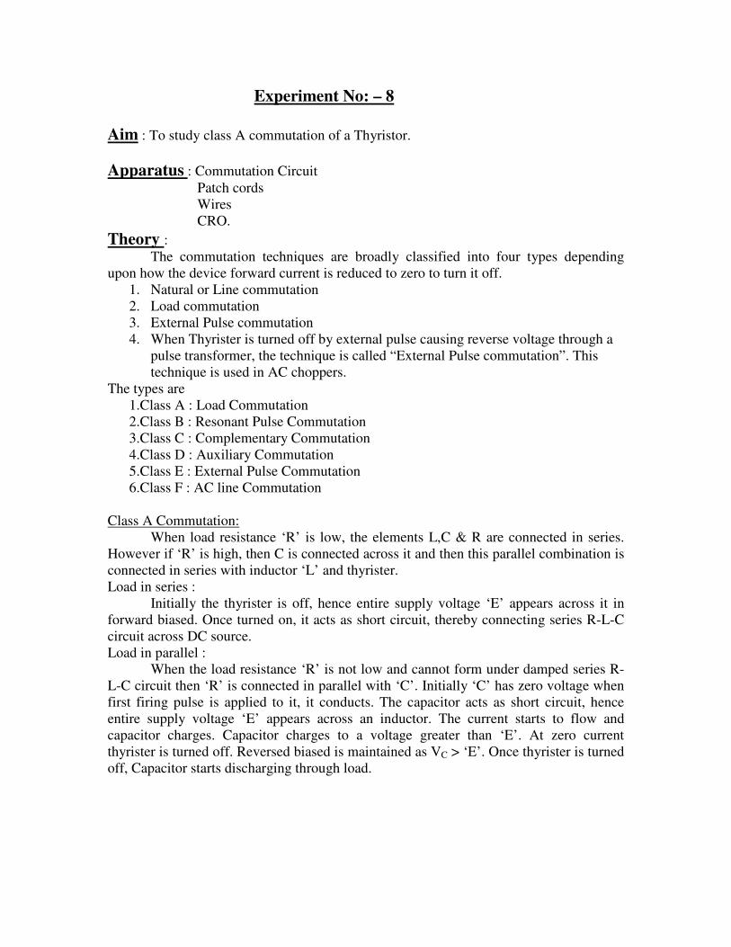
Experiment No: – 8 Aim : To study class A commutation of a Thyristor. Apparatus : Commutation Circuit
Patch cords Wires CRO.
Theory : The commutation techniques are broadly classified into four types depending
upon how the device forward current is reduced to zero to turn it off. 1. Natural or Line commutation 2. Load commutation 3. External Pulse commutation 4. When Thyrister is turned off by external pulse causing reverse voltage through a
pulse transformer, the technique is called “External Pulse commutation”. This technique is used in AC choppers.
The types are 1.Class A : Load Commutation 2.Class B : Resonant Pulse Commutation 3.Class C : Complementary Commutation 4.Class D : Auxiliary Commutation 5.Class E : External Pulse Commutation 6.Class F : AC line Commutation
Class A Commutation: When load resistance ‘R’ is low, the elements L,C & R are connected in series. However if ‘R’ is high, then C is connected across it and then this parallel combination is connected in series with inductor ‘L’ and thyrister. Load in series : Initially the thyrister is off, hence entire supply voltage ‘E’ appears across it in forward biased. Once turned on, it acts as short circuit, thereby connecting series R-L-C circuit across DC source. Load in parallel : When the load resistance ‘R’ is not low and cannot form under damped series R-L-C circuit then ‘R’ is connected in parallel with ‘C’. Initially ‘C’ has zero voltage when first firing pulse is applied to it, it conducts. The capacitor acts as short circuit, hence entire supply voltage ‘E’ appears across an inductor. The current starts to flow and capacitor charges. Capacitor charges to a voltage greater than ‘E’. At zero current thyrister is turned off. Reversed biased is maintained as VC > ‘E’. Once thyrister is turned off, Capacitor starts discharging through load.
Circuit Diagram :
Procedure : 1.Study the circuit provided. 2.Switch on the power supply. 3.note the output waveforms. 4.Plot the waveforms. Result : Class A commutation technique is studied and graphs are plotted. Viva Questions:- 1)What do you mean by commutation method? 2)What do understand by forced commutation method?
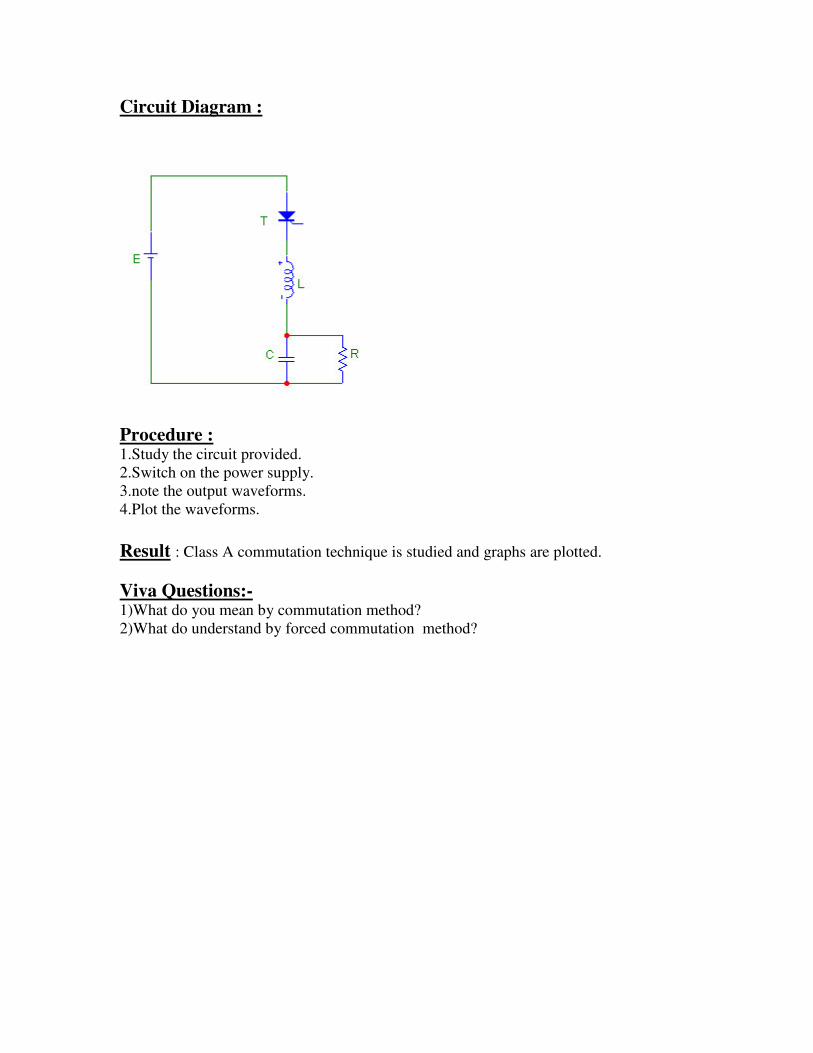
Experiment No: –9 Aim:- To study DC chopper circuit. Apparatus:-Experimental kit
Patch chord CRO probe Rheostat Supply voltage
Theory:- Operation of DC CHOOPER
Chopper is a switching circuits, which converts the fixed I/p dc voltage into variable dc o/p voltage. Chopper can be used where the variable o/p dc voltage is required .e.g. trolley cars, buses, marine hoists, lift, electrical locomotives in which speed control & breaking can be achieved using DC chopper.
Chopper system enables smooth control , fast response and high frequency .there are basically of two types of chopper:-
a) step up chopper. b) step down chopper. a) Step down chopper:-In step down chopper the average o/p load voltage is less
than I/p voltage. b) Step up chopper :-In step up chopper ,the average o/p and load voltage is more
than I/p supply voltage. Circuit diagram:-
Procedure :-
1) Study the circuit diagram. 2) Make connections as shown in circuit diagram. 3) Supply a trigger pulse to the gate terminal of thyristor . 4) Switch on the DC supply . 5) Connect CRO probe to obtained the output. 6) Note the TON and TOFF time of wave form obtained on screen and plot the output
on graph paper.

Result :- DC chopper is studied and o/p waveform is plotted. Viva Questions:- 1)What do you mean by step up chopper? 2)What are the applications of chopper?
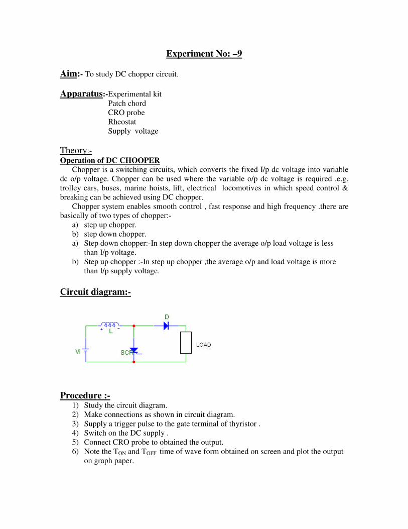
Experiment No:– 10 Aim : To study single-phase converter. Apparatus : One phase converter circuit
Patch cords Wires, Dimmerstate.
Theory : There are two basic configurations of full wave controlled rectifiers. This classification is based on the types of SCR.
1. Midpoint Converters 2. Bridge Converters.
In one phase full wave controlled rectifier circuit with midpoint configuration, two SCR’s, a one-phase transformer with center tapped secondary windings is employed. Effect of overlap angle : Effect of source inductor in delaying current commutation. The overlap angle ‘µ’ and corresponding reduction in average DC output voltage is function of load current and source inductance. For a given value of I, overlap angle ‘µ’ will increase with load current. As overlap angle increases, the circuit will go into various modes of operation. In one phase circuit as long as ‘µ’ is less than ‘π’ for output voltage will be valid. When µ=π, load will be permanently shorted by the SCR’s and the output voltage will be zero because during the overlap period all the SCR’s will be conducting. Firing Source :
1. Cosine wave crossing pulse timing control. 2. Internal control schemes 3. Scheme using phase locked oscillator 4. Digital firing schemes
Circuit Diagram :

Procedure : 1. Study the circuit provided. 2. Connect CRO to the circuit using CRO probes. 3. Switch on the power supply. 4. Note the o/p waveforms for different values of firing angle. 5. Plot the waveform.
Result : A single-phase converter was studied successfully. Viva Questions:- 1)What is single-phase half controlled converter? 2)What are the different types of single-phase half controlled bride converter?


![G.H.RAISONI COLLEGE OF ENGINEERING,NAGPUR …raisoni.net/raisoniad/download/5ETC_MPI.pdf · Branch:-5th Semester[Electronics & Telecommunication] Subject:-Microprocessor and ... Sign](https://img.dokumen.tips/doc/110x75/5b1dc5a87f8b9a8e158bcb9b/ghraisoni-college-of-engineeringnagpur-branch-5th-semesterelectronics-.jpg)