Embed Size (px)
Citation preview
General Methodology to Develop Statistical Compact MOS Models
for VLSI Circuit Simulation
Samar K. SahaSuVolta, Inc.
Los Gatos, CA 95032
March 16, 2012
MOS-AK/GSA 2012, MARCH 16-18, NOIDA, INDIA
Slide 2
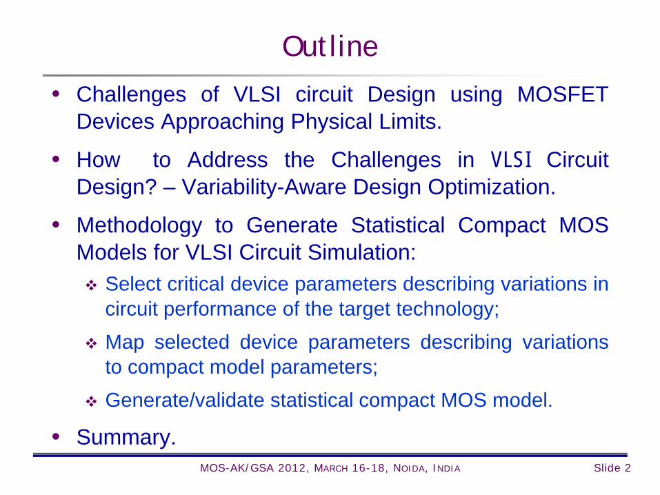
Outline
• Challenges of VLSI circuit Design using MOSFETDevices Approaching Physical Limits.
• How to Address the Challenges in VLSI CircuitDesign? – Variability-Aware Design Optimization.
• Methodology to Generate Statistical Compact MOSModels for VLSI Circuit Simulation: Select critical device parameters describing variations in
circuit performance of the target technology; Map selected device parameters describing variations
to compact model parameters; Generate/validate statistical compact MOS model.
• Summary.MOS-AK/GSA 2012, MARCH 16-18, NOIDA, INDIA

Slide 3
Outline
• Challenges of VLSI circuit Design using MOSFETDevices Approaching Physical Limits.
• How to Address the Challenges in VLSI CircuitDesign? – Variability-Aware Design Optimization.
• Methodology to Generate Statistical Compact MOSModels for VLSI Circuit Simulation: Select critical device parameters describing variations in
circuit performance of the target technology; Map selected device parameters describing variations
to compact model parameters; Generate/validate statistical compact MOS model.
• Summary.MOS-AK/GSA 2012, MARCH 16-18, NOIDA, INDIA
Slide 4
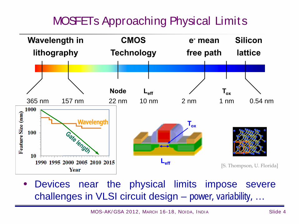
MOSFETs Approaching Physical Limits
2 nm 0.54 nm
e- mean free path
Silicon lattice
22 nm 10 nm
CMOS Technology
Node Leff
1 nmTox
Leff
Tox
[S. Thompson, U. Florida]
157 nm
Wavelength in lithography
365 nm
Wavelength
• Devices near the physical limits impose severechallenges in VLSI circuit design – power, variability, …
MOS-AK/GSA 2012, MARCH 16-18, NOIDA, INDIA

Slide 5
Design Challenges – Lower Power
• Energy efficiency and power are the dominant issuesin today’s computing and communications products: Mobile computing everywhere are affected by the
limited battery life Cloud computing requires power reduction for extended
Google searches Siri speech processing.
• The power is given by: Power ~ CV2 f + I.V
• In order to lower power, the supply voltage (V) mustbe decreased.
Switching/activepower
Leakage/staticpower
MOS-AK/GSA 2012, MARCH 16-18, NOIDA, INDIA
Slide 6
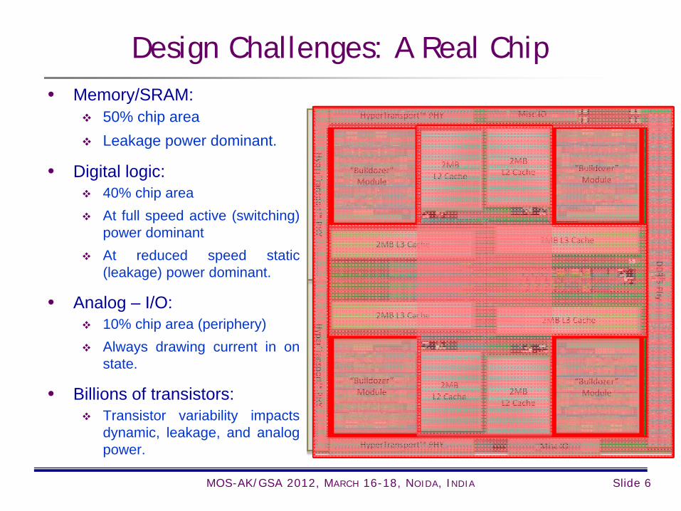
• Memory/SRAM: 50% chip area Leakage power dominant.
• Digital logic: 40% chip area At full speed active (switching)
power dominant At reduced speed static
(leakage) power dominant.
• Analog – I/O: 10% chip area (periphery) Always drawing current in on
state.
• Billions of transistors: Transistor variability impacts
dynamic, leakage, and analogpower.
Design Challenges: A Real Chip
MOS-AK/GSA 2012, MARCH 16-18, NOIDA, INDIA

Slide 7
Impact of Transistor Variability: Leakage
• Transistor threshold voltage (VTH) indicates transistor variability.• Leakage current is exponentially dependent on VTH.• Lower VTH variability (VT) reduces number of leaky low VTH devices.• Power dissipation is dominated by low VTH edge of distribution.• Smaller VT Less leakage power for digital and memory/SRAM.
High leakage tail
High leakage tail dominates power
2.7x higher power(85mV subVT slope)
High VT tailSlows down ICs
MOS-AK/GSA 2012, MARCH 16-18, NOIDA, INDIA
Slide 8
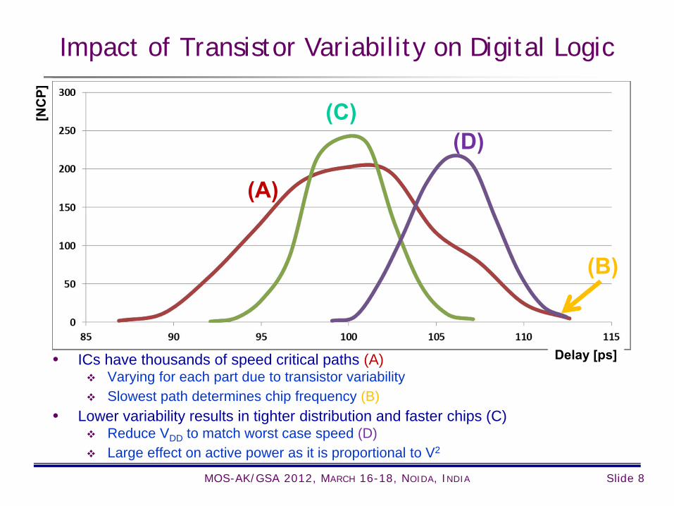
Impact of Transistor Variability on Digital Logic
• ICs have thousands of speed critical paths (A) Varying for each part due to transistor variability Slowest path determines chip frequency (B)
• Lower variability results in tighter distribution and faster chips (C) Reduce VDD to match worst case speed (D) Large effect on active power as it is proportional to V2
[NC
P]
Delay [ps]
(B)
(A)
(C)(D)
MOS-AK/GSA 2012, MARCH 16-18, NOIDA, INDIA

Slide 9
Outline
• Challenges of VLSI circuit Design using MOSFETDevices Approaching Physical Limits.
• How to Address the Challenges in VLSI CircuitDesign? – Variability-Aware Design Optimization.
• Methodology to Generate Statistical Compact MOSModels for VLSI Circuit Simulation: Select critical device parameters describing variations in
circuit performance of the target technology; Map selected device parameters describing variations
to compact model parameters; Generate/validate statistical compact MOS model.
• Summary.MOS-AK/GSA 2012, MARCH 16-18, NOIDA, INDIA
Slide 10
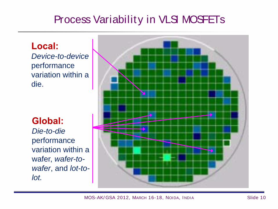
Process Variability in VLSI MOSFETs
Local:Device-to-deviceperformance variation within a die.
Global:Die-to-dieperformance variation within a wafer, wafer-to-wafer, and lot-to-lot.
MOS-AK/GSA 2012, MARCH 16-18, NOIDA, INDIA
Slide 11
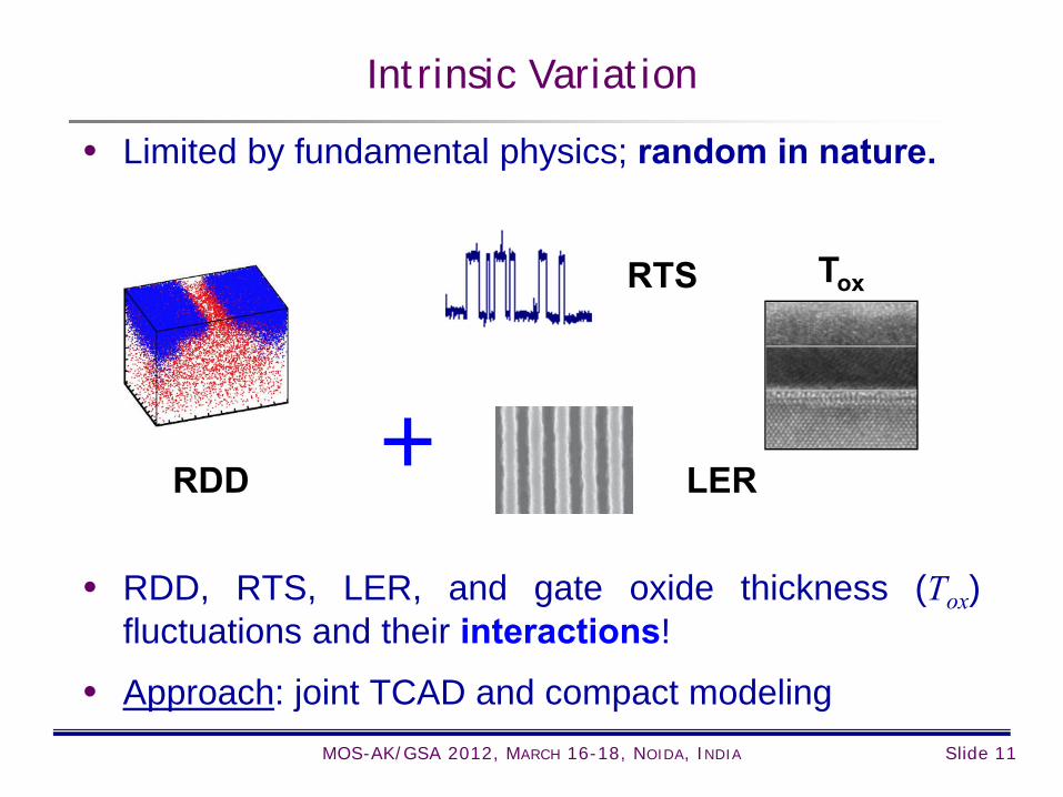
Intrinsic Variation
• Limited by fundamental physics; random in nature.
• RDD, RTS, LER, and gate oxide thickness (Tox)fluctuations and their interactions!
• Approach: joint TCAD and compact modeling
RDD
RTS
+
Tox
LER
MOS-AK/GSA 2012, MARCH 16-18, NOIDA, INDIA

Slide 12
Process Induced Variation
• Induced by the manufacturing process; systematic.
• Usually exhibit layout pattern dependence.
• Approach: Compact modeling and in-situcharacterization under various process and designconditions.
NRG HK/MG
WPE BEOLRTA
Stress
MOS-AK/GSA 2012, MARCH 16-18, NOIDA, INDIA
Slide 13
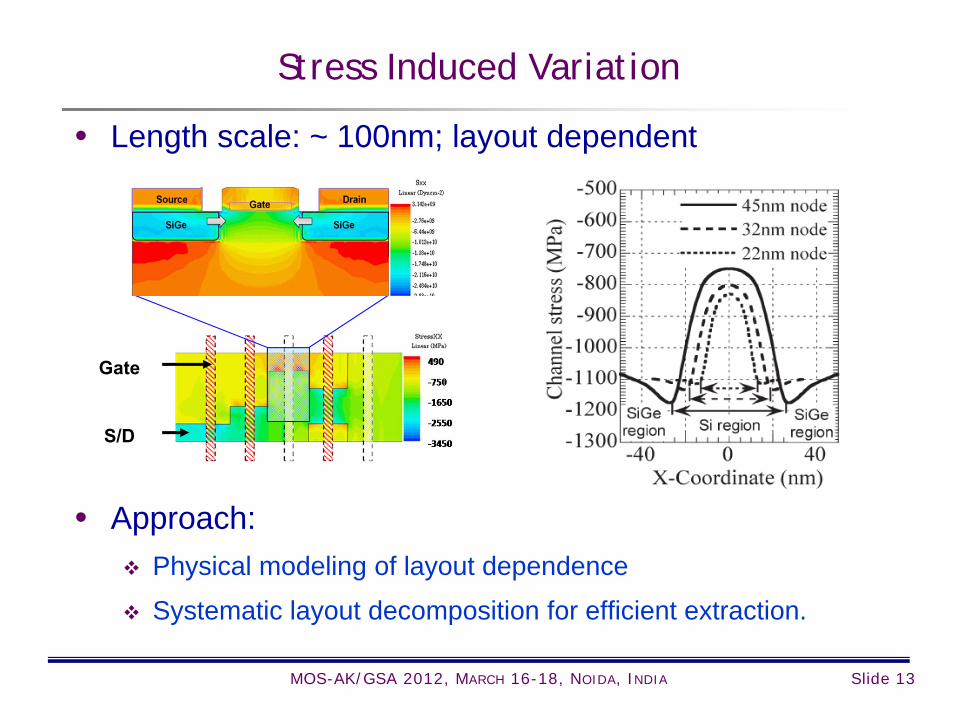
Stress Induced Variation
• Length scale: ~ 100nm; layout dependent
• Approach: Physical modeling of layout dependence
Systematic layout decomposition for efficient extraction.
Gate
S/D
MOS-AK/GSA 2012, MARCH 16-18, NOIDA, INDIA

Slide 14
Compact Model for Variability-Aware Circuit Design
• Compact model for variability-aware circuit design: Must include accurate statistical
data on process variability: Chip-to-chipMismatch Layout effects;
Must be computationally efficient Simulation time Design optimization Design analysisSimple and ease of use.
Transistor Model
…...
Path Timing
T0 +3-3
Path Timing
T0 +3-3
L Vth
MOS-AK/GSA 2012, MARCH 16-18, NOIDA, INDIA

Slide 15
Outline
• Challenges of VLSI circuit Design using MOSFETDevices Approaching Physical Limits.
• How to Address the Challenges in VLSI CircuitDesign? – Variability-Aware Design Optimization.
• Methodology to Generate Statistical Compact MOSModels for VLSI Circuit Simulation: Select critical device parameters describing variations in
circuit performance of the target technology; Map selected device parameters describing variations
to compact model parameters; Generate/validate statistical compact MOS model.
• Summary.MOS-AK/GSA 2012, MARCH 16-18, NOIDA, INDIA
Slide 16
Critical MOSFET Device Parameters
• Compact variability modeling must account for: Local process (Intra-die) variability or mismatch (P) of
a parameter, P between identical paired-transistors
Global process variability of P between,Die-to-die (Inter-die)Wafer-to-wafer Lot-to-lot.
• Statistically, each value of P and P converges to aGaussian distribution with ‘0’ mean for a large numberof samples.
Here, P is a parameter of an advanced compact MOSmodel, e.g. BSIM4.
MOS-AK/GSA 2012, MARCH 16-18, NOIDA, INDIA

Slide 17
Device Parameters to Model Mismatch
The variance of relative MOSFET drain current, IDSmismatch due to process variability can be shown as:
WherePi = randomly varying function of ith device parameterPi = mismatch in Pi between identical paired-transistorsPi = standard deviation in Pi
(Pi, Pi+1) = correlation between the mismatches in Piand Pi+1.
n
i1iPiPii
i
DS
i
DS
DS
n
iiP
i
DS
DSDSIDSI
PPρPI
PI
I
PI
I
11
12
1
22
2
,.2
1
MOS-AK/GSA 2012, MARCH 16-18, NOIDA, INDIA
Slide 18
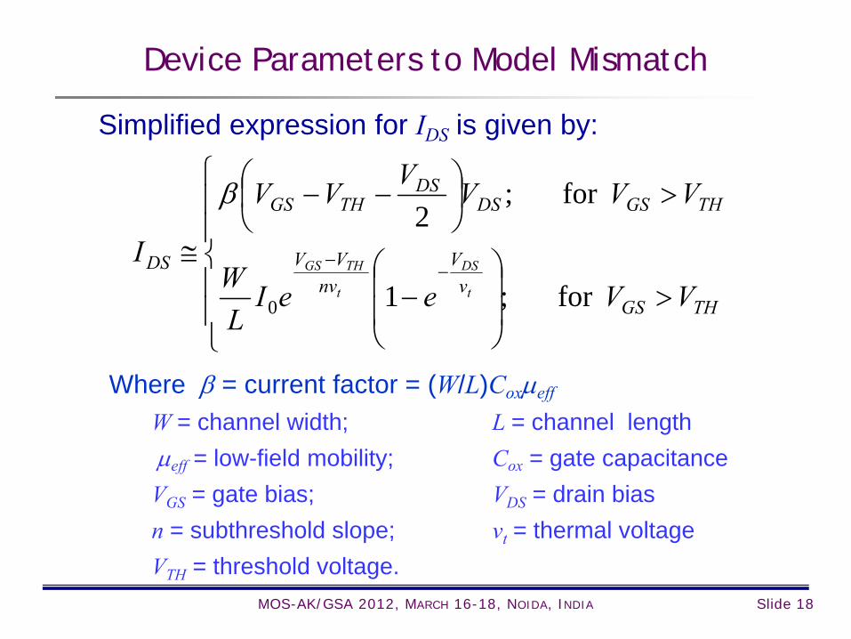
Device Parameters to Model Mismatch
Simplified expression for IDS is given by:
Where = current factor = (W/L)Coxeff
W = channel width; L = channel lengtheff = low-field mobility; Cox = gate capacitanceVGS = gate bias; VDS = drain biasn = subthreshold slope; vt = thermal voltageVTH = threshold voltage.
THGSv
Vnv
VV
THGSDSDS
THGS
DS
VVeeIL
W
VVVVVV
It
DS
t
THGS
for ;1
for ;2
0
MOS-AK/GSA 2012, MARCH 16-18, NOIDA, INDIA

Slide 19
Device Parameters to Model Mismatch
• IDS mismatch between two identical-paired transistorsdue to process variations can be described by: P1 = VTH
P2
• The variance of relative IDS mismatch is given by:
WhereVTH = mismatch in VTH
= mismatch in
TH
THDSDS
VTHDS
TH
DS
DS
DS
DSV
TH
DS
DSII
VIVI
I
IIV
II
,.2
11
2
22
22
2
MOS-AK/GSA 2012, MARCH 16-18, NOIDA, INDIA
Slide 20
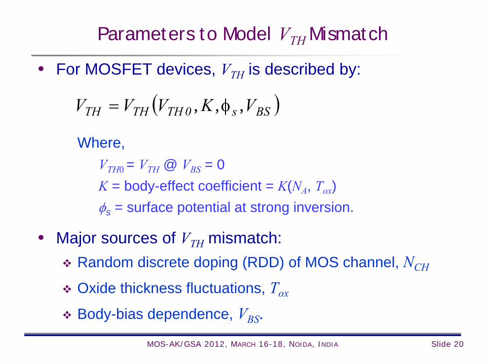
Parameters to Model VTH Mismatch
• For MOSFET devices, VTH is described by:
Where,VTH0 = VTH @ VBS = 0K = body-effect coefficient = K(NA, Tox)s = surface potential at strong inversion.
• Major sources of VTH mismatch: Random discrete doping (RDD) of MOS channel, NCH
Oxide thickness fluctuations, Tox
Body-bias dependence, VBS.
BSs0THTHTH VKVVV ,,,
MOS-AK/GSA 2012, MARCH 16-18, NOIDA, INDIA
Slide 21
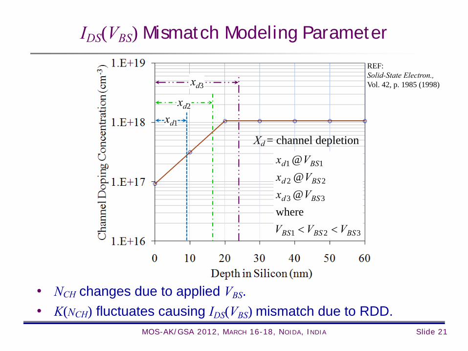
IDS(VBS) Mismatch Modeling Parameter
• NCH changes due to applied VBS.• K(NCH) fluctuates causing IDS(VBS) mismatch due to RDD.
321
33
22
11
where@@@
BSBSBS
BSd
BSd
BSd
VVV
VxVxVx
xd1
xd2
xd3
Xd = channel depletion
REF: Solid-State Electron., Vol. 42, p. 1985 (1998)
MOS-AK/GSA 2012, MARCH 16-18, NOIDA, INDIA

Slide 22
Parameters to Model Mismatch
• From simplified IDS expression, fluctuations impactIDS mismatch for VGS > VTH:
Here,
• The current factor fluctuations are caused by: Mismatch in W and L due to line-edge roughness (LER)
and line-width roughness (LWR) Mismatch in Cox(Tox) Mismatch in channel inversion carrier mobility, eff.
DSDS
THGSDS VVVVI
2
),,,( effoxeffox CLWβCL
Wβ
MOS-AK/GSA 2012, MARCH 16-18, NOIDA, INDIA
Slide 23
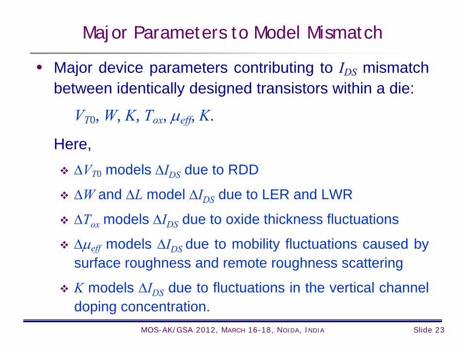
Major Parameters to Model Mismatch
• Major device parameters contributing to IDS mismatchbetween identically designed transistors within a die:
VT0, W, K, Tox, eff, K.
Here, VT0 models IDS due to RDD
W and L model IDS due to LER and LWR
Tox models IDS due to oxide thickness fluctuations
eff models IDS due to mobility fluctuations caused bysurface roughness and remote roughness scattering
K models IDS due to fluctuations in the vertical channeldoping concentration.
MOS-AK/GSA 2012, MARCH 16-18, NOIDA, INDIA

Slide 24
Major Parameters to Model Global Variability
• From simplified IDS expression, the major deviceparameters impacted by global process variability are:VTH, W, L, Tox, eff.
• Across the chip variation in IDS can be described by: VTH = average fluctuations in VTH
W and L = average fluctuations in W and L Tox = average shift in Tox
Rds = average fluctuations in source/drain (S/D)resistance due to corresponding fluctuations in implants
eff = average fluctuations in eff
Cov = average shift in gate capacitance CJ = average fluctuations in S/D junction capacitance.
MOS-AK/GSA 2012, MARCH 16-18, NOIDA, INDIA

Slide 25
Outline
• Challenges of VLSI circuit Design using MOSFETDevices Approaching Physical Limits.
• How to Address the Challenges in VLSI CircuitDesign? – Variability-Aware Design Optimization.
• Methodology to Generate Statistical Compact MOSModels for VLSI Circuit Simulation: Select critical device parameters describing variations in
circuit performance of the target technology; Map selected device parameters describing variations
to compact model parameters; Generate/validate statistical compact MOS model.
• Summary.MOS-AK/GSA 2012, MARCH 16-18, NOIDA, INDIA
Slide 26
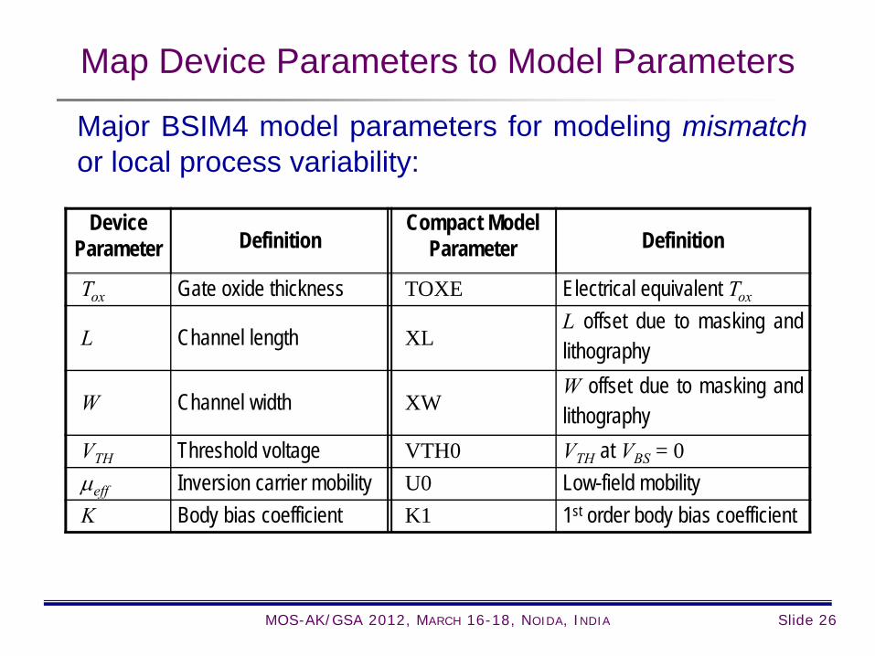
Map Device Parameters to Model Parameters
Device Parameter Definition
Compact Model Parameter Definition
Tox Gate oxide thickness TOXE Electrical equivalent Tox
L Channel length XLL offset due to masking andlithography
W Channel width XWW offset due to masking andlithography
VTH Threshold voltage VTH0 VTH at VBS = 0eff Inversion carrier mobility U0 Low-field mobilityK Body bias coefficient K1 1st order body bias coefficient
Major BSIM4 model parameters for modeling mismatchor local process variability:
MOS-AK/GSA 2012, MARCH 16-18, NOIDA, INDIA

Slide 27
Map Device Parameters to Model Parameters
Device Parameter Definition Compact Model
Parameter Definition
Tox Gate oxide thickness TOXE Electrical equivalent Tox
L Channel length XL L offset due to masking and lithography
W Channel width XW W offset due to masking and lithography
VTH Threshold voltage VTH0 VTH at VBS = 0 eff Inversion carrier mobility U0 Low-field mobility K Body bias coefficient K1 1st order body bias coefficient RDS S/D extension resistance RDSW Zero-bias RDS
Cov Gate overlap capacitance CGSL / CGDL S/D extension Cov CGSO / CGDO Non-S/D region Cov
CJ
S/D junction capacitance
CJS / CJD Area component of CJ CJSWS / CJSWD Isolation-edge side-wall CJ CJSWGS/CJSWGD Gate-edge side-wall CJ
Major BSIM4 model parameters for modeling global process variability:
MOS-AK/GSA 2012, MARCH 16-18, NOIDA, INDIA

Slide 28
Outline
• Challenges of VLSI circuit Design using MOSFETDevices Approaching Physical Limits.
• How to Address the Challenges in VLSI CircuitDesign? – Variability-Aware Design Optimization.
• Methodology to Generate Statistical Compact MOSModels for VLSI Circuit Simulation: Select critical device parameters describing variations in
circuit performance of the target technology; Map selected device parameters describing variations
to compact model parameters; Generate/validate statistical compact MOS model.
• Summary.MOS-AK/GSA 2012, MARCH 16-18, NOIDA, INDIA
Slide 29
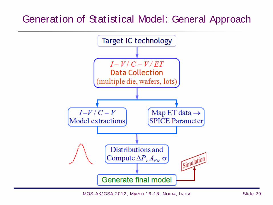
Generation of Statistical Model: General Approach
MOS-AK/GSA 2012, MARCH 16-18, NOIDA, INDIA

Slide 30
Local Component of Variability Model
• The mismatch in model parameter Pi is modeled by:
Where Pi = compact model parameters accounting for local
process variability N(0, Pi) = normal distribution of Pi
Pi is computed using Pelgrom’s law:
Here Api = constantW = width of the device L = length of the device = number of variance, typically ~ 1.
),0(),0(, NNPii PPmismatchi
WL
Ai
i
pP
MOS-AK/GSA 2012, MARCH 16-18, NOIDA, INDIA

Slide 31
Global Component of Variability Model
• The global variation in parameter Pi is modeled by:
Where, i = variance in Pi accounting for global process variability
N(0, i) = normal distribution of Pi
= number of variance due to global process variability,typically ~ 3.
modelcorner fixedfor ;
model Carlo Montefor );,0(,
i
iglobali
NP
MOS-AK/GSA 2012, MARCH 16-18, NOIDA, INDIA
Slide 32
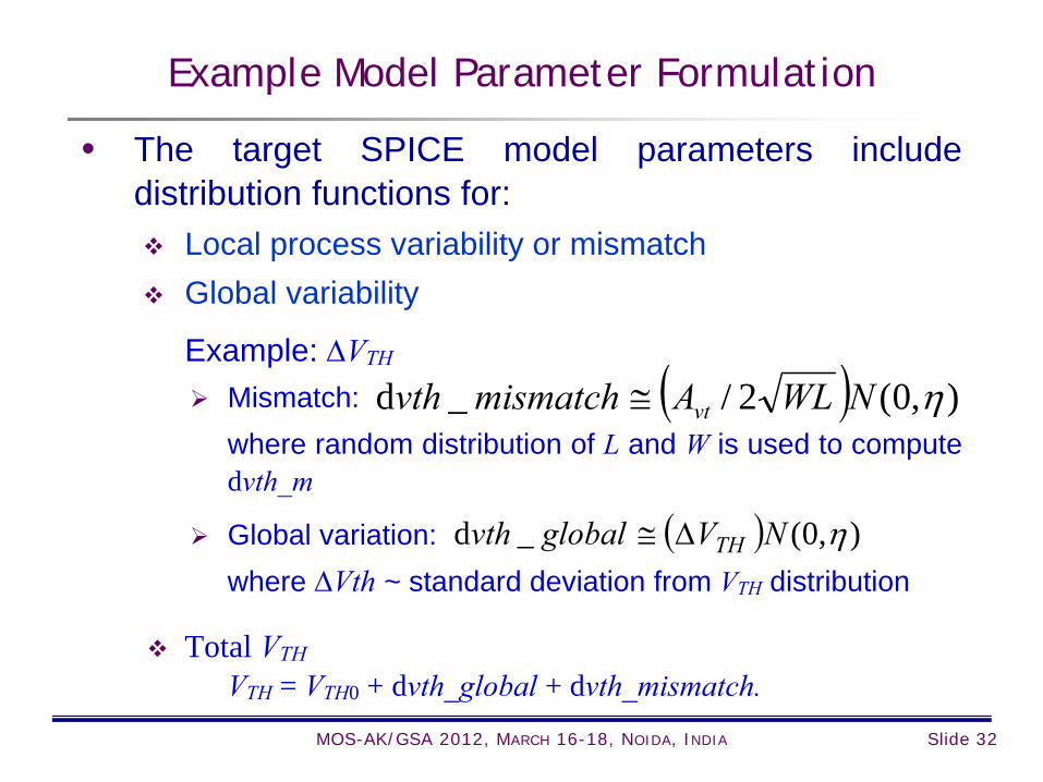
Example Model Parameter Formulation
• The target SPICE model parameters includedistribution functions for: Local process variability or mismatch Global variability
Example: VTH
Mismatch:where random distribution of L and W is used to computedvth_m
Global variation:where Vth ~ standard deviation from VTH distribution
Total VTH
VTH = VTH0 + dvth_global + dvth_mismatch.
),0(2/_d NWLAmismatchvth vt
),0(_d NVglobalvth TH
MOS-AK/GSA 2012, MARCH 16-18, NOIDA, INDIA

Slide 33
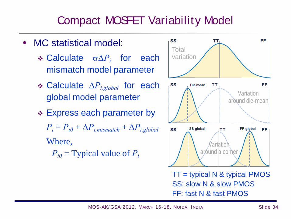
Compact MOSFET Variability Model
• MC statistical model: Calculate Pi for each mismatch model parameter Calculate Pi,global for each global model parameter Express Pi = Pi0 + Pi,mismatch + Pi,global
Where, Pi0 = typical value of Pi
• Fixed corner with mismatch model: Use Pi for each global model parameters with value of
3 3 Use fixed value of 1-value of Pi calculated by
Pelgrom’s law for each mismatch model parameter Express each parameter by
Pi = Pi0 + Pi,global + Pi,mismatch (fixed)MOS-AK/GSA 2012, MARCH 16-18, NOIDA, INDIA
Slide 34
Compact MOSFET Variability Model
• MC statistical model: Calculate Pi for each
mismatch model parameter
Calculate Pi,global for eachglobal model parameter
Express each parameter byPi = Pi0 + Pi,mismatch + Pi,global
Where,Pi0 = Typical value of Pi
TT = typical N & typical PMOSSS: slow N & slow PMOSFF: fast N & fast PMOS
Total variation
Variationaround die-mean
Variationaround a corner
MOS-AK/GSA 2012, MARCH 16-18, NOIDA, INDIA

Slide 35
Compact MOSFET Variability Model
• Fixed corner model with mismatch: Use Pi for each global model parameters with value of
3 3 Use fixed value of 1-value of Pi calculated by
Pelgrom’s law for each mismatch model parameter Express each parameter by
Pi = Pi0 + Pi,global + Pi,mismatch (fixed)TT FF
3σglobalSS3σglobal
SS-total3σglobal+ 1σmismatch
FF-total3σglobal+ 1σmismatch
MOS-AK/GSA 2012, MARCH 16-18, NOIDA, INDIA
Slide 36
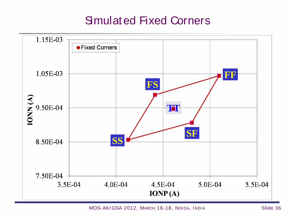
Simulated Fixed Corners
FF
SFSS
FS
TT
MOS-AK/GSA 2012, MARCH 16-18, NOIDA, INDIA
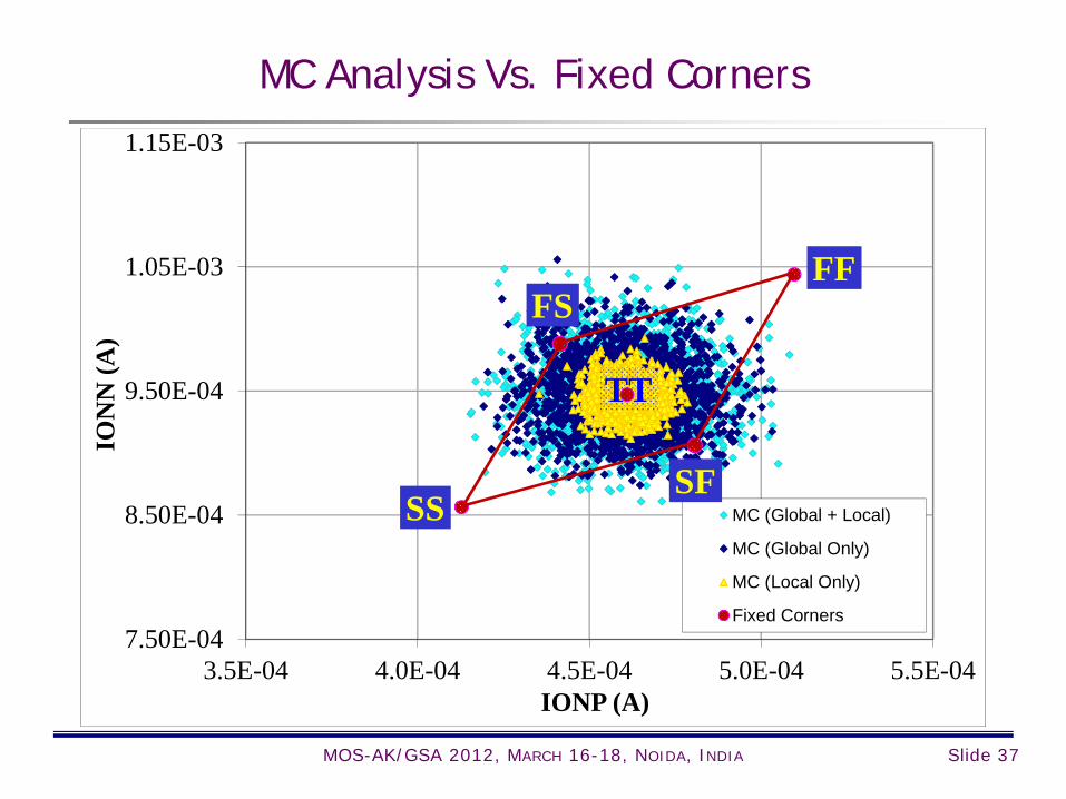
Slide 37
MC Analysis Vs. Fixed Corners
7.50E-04
8.50E-04
9.50E-04
1.05E-03
1.15E-03
3.5E-04 4.0E-04 4.5E-04 5.0E-04 5.5E-04
ION
N (A
)
IONP (A)
MC (Global + Local)
MC (Global Only)
MC (Local Only)
Fixed Corners
FF
SFSS
FS
TT
MOS-AK/GSA 2012, MARCH 16-18, NOIDA, INDIA
Slide 38
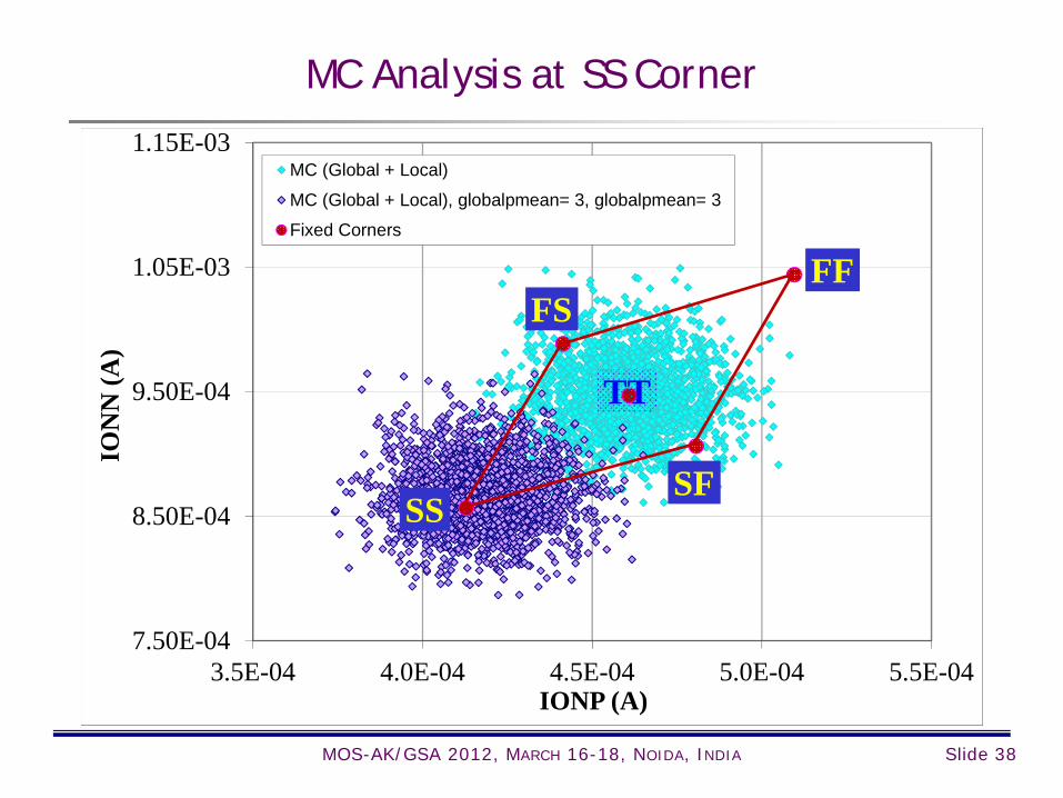
MC Analysis at SS Corner
7.50E-04
8.50E-04
9.50E-04
1.05E-03
1.15E-03
3.5E-04 4.0E-04 4.5E-04 5.0E-04 5.5E-04
ION
N (A
)
IONP (A)
MC (Global + Local)
MC (Global + Local), globalpmean= 3, globalpmean= 3
Fixed Corners
FF
SFSS
FS
TT
MOS-AK/GSA 2012, MARCH 16-18, NOIDA, INDIA

Slide 39
MC Analysis at FF Corner
7.50E-04
8.50E-04
9.50E-04
1.05E-03
1.15E-03
3.5E-04 4.0E-04 4.5E-04 5.0E-04 5.5E-04
ION
N (A
)
IONP (A)
MC (Global + Local)
MC (Global + Local), globalnmean= -3, globalpmean= -3
Fixed Corners
FF
SFSS
FS
TT
MOS-AK/GSA 2012, MARCH 16-18, NOIDA, INDIA
Slide 40
Outline
• Challenges of VLSI circuit Design using MOSFETDevices Approaching Physical Limits.
• How to Address the Challenges in VLSI CircuitDesign? – Variability-Aware Design Optimization.
• Methodology to Generate Statistical Compact MOSModels for VLSI Circuit Simulation: Select critical device parameters describing variations in
circuit performance of the target technology; Map selected device parameters describing variations
to compact model parameters; Generate/validate statistical compact MOS model.
• Summary.MOS-AK/GSA 2012, MARCH 16-18, NOIDA, INDIA

Slide 41
Summary
• Compact variability model is critical to addressperformance fluctuations in VLSI devices, circuits,and systems due to: Local process variation Global process variation.
• Basic steps for compact variability modeling includes: Determining the critical sources of process variability Characterizing device performance to determine critical
device parameters modeling process variability Mapping device parameters to compact model
parameters Generating MC and fixed/user-defined corner models.
MOS-AK/GSA 2012, MARCH 16-18, NOIDA, INDIA

Slide 42MOS-AK/GSA 2012, MARCH 16-18, NOIDA, INDIA