Embed Size (px)
Citation preview

GEM Simulation & Test
Xinzhan Bai
China Institute of Atomic Energy
2012-07-18 KITPC, Beijing, China 1

Outline
1. Introduction
2. GEM Simulation
3. GEM foil
4. JLab GEM Test
5. Summary
2012-07-18 KITPC, Beijing, China 2

Introduction 1. Core Part: GEM Foil.
2. Typical GEM Foil has 3 layers, two 5-micron thick copper foils and one 50-micron thick kapton foil in the middle.
3. The foil is patterned with an array of holes.
4. Diameter of the hole is 70 microns, and the distance between them is 140 microns.
5. Apply electric voltages on the two copper layers.
6. Electric Field is very strong in the hole area, and weak outside the hole area.
2012-07-18 KITPC, Beijing, China 3
GEM Foil
GEM Field

Introduction
1. Avalanche happens in the hole area only. This improves the spatial resolution in a large extent.
2. For the triple-foil GEM detector, the total gain is the multiply of the gain of each gem foil.
2012-07-18 KITPC, Beijing, China 4
Triple-Foil GEM Detector

Introduction
1. Six layers of GEM detectors in all.
2. SIDIS (Semi-Inclusive Deep Inelastic Scattering) experiment is one kind of the experiments that will be conducted on this spectrometer.
2012-07-18 KITPC, Beijing, China 5
SoLID Spectrometer

Different (e,e’h) experimental configurations
Experiments Luminosity
(s·cm2)-1
Tracking Area
(cm2)
Resolution
Angular
(mrad)
Vertex
(mm)
Momentum
(%)
GMn - GEn
up to 7·1037 40x150
and 50x200 < 1 <2 0.5%
GEp(5)
up to 8·1038
40x120,
50x200 and
80x300
<0.7
~1.5 ~ 1 0.5%
SIDIS
up to 2·1037
40x120,
40x150 and
50x200 ~ 0.5 ~1 <1%
20
12
-07
18
K
ITP
C, B
eijin
g, C
hin
a 6
Maximum reusability: same trackers in different setups
High Rates Large Area Down to ~ 70 μm spatial resolution
Refer to GEM status by Evaristo

Outline
1. Introduction
2. GEM Simulation
3. GEM foil
4. JLab GEM Test
5. Summary
2012-07-18 KITPC, Beijing, China 7

GEM Simulation
1. Maxwell + neBEM for the electric field calculation.
2. Garfield + Magboltz + Heed for the Calculation of electron transportation in Gas.
3. We simulated the Spatial Resolution, Gain, Electron Transparency of gem foils, and the Counting Rate.
2012-07-18 KITPC, Beijing, China 8
Avalanche in a Single-Foil GEM Detector

Electric Field Distribution 1. Electric Field Distribution
along the line which is perpendicular to the GEM foil and crossing the center of a hole.
2. Electric field reaches its maximum value at the center of the hole.
3. During our simulation, avalanche won’t happen when E < 5 kV/cm, thus avalanche only happens in the hole area.
2012-07-18 KITPC, Beijing, China 9
Field Distribution on a line crossing the centre of a hole
Collection Area Drift Area

σ = 73.6 microns σ = 86.7 microns
Spatial Resolution
2012-07-18 KITPC, Beijing, China 10
Avalanche Cluster Distribution on the Readout Plane

Electron Transparency
20 50 80 100 200 300 400 500 600 700 800 900 1000 1100 1200 1300 1400 1500
0
5
10
15
20
25
30
35
40
45
50
Tran
spar
ency
%
Transparency Vs. V_Drift
Transparency is dependent to the voltages applied on the drift area, collection area and gem foil.
When two of them are fixed, how the transparency varies with the third one?
2012-07-18 KITPC, Beijing, China 11
V_Drift
V_Drift
V_Collect
V_Gem

Electron Transparency
200 300 400 500 600 700 800 900 1000 1100 1200 1300 1400 1500
0
5
10
15
20
25
30
35
40
45
50
V_GEM
Tran
spar
ency
%
Trans. Vs. V_Gem
2012-07-18 KITPC, Beijing, China 12

Electron Transparency
100 200 300 400 500 600 700 800 900 1000 1100 1200 1300 1400 1500 1600
0
5
10
15
20
25
30
35
40
45
50
V_Collect
Tran
spar
ency
%
Trans. Vs. V_Collect
2012-07-18 KITPC, Beijing, China 13

Gain
Distribution of Gain of Single-Layer GEM Detector
RMS Mean
= 0.6
2012-07-18 KITPC, Beijing, China 14
Energy Resolution of GEM detectors is dependent to its gain performance. Gain is not stable both from the experiment and from the simulation.
Gain
600 700 800
0
0.5
1
1.5
2
2.5
3
3.5
4
4.5
V_GEM
Log1
0 (
Gai
n )
Gain & Effective Gain vs. V_GEM
100 200 300 400 500 600 700 800-0.5
0
0.5
1
1.5
2
2.5
3
3.5
4
V_GEM lo
g10
(G
ain
) Gain vs. V_GEM
2012-07-18 KITPC, Beijing, China 15
How gain varies with the voltage applied on the GEM foil. Gain: Number of electrons from all of the avalanches. Effective Gain: Number of electrons that reach the readout board.

Counting Rate
1. Shut down the attachment process, there will be two ends for ions.
2. Trapped by GEM foils and Trapped by the Drift Electrode.
3. Most of the ions will be trapped by gem foils, where they are produced, which leads to a very short drifting time for ions.
2012-07-18 KITPC, Beijing, China 16
Ion Drifting Time Distribution
Trapped by GEM foils
Trapped by Drift Electrode
μs

Outline
1. Introduction
2. GEM Simulation
3. GEM foil
4. JLab GEM Test
5. Summary
2012-07-18 KITPC, Beijing, China 17

The Construction of Clean Room at CIAE for GEM Foil R&D
Mask plate from CIAE
50um diameter
Mask plate from CERN
60um diameter
After half year negotiation, CIAE has signed officially the LICENSE AGREEMENT FOR MANUFACTURING AND COMMERCIALISATION OF GEM FOILS AND GEM-BASED PRODUCTS with CERN, and will get full technology support from CERN.
8/16/2012 18 China Institute of Atomic Energy

1. We can reach a minimum thickness of 12 microns of the copper foil coated on the Kapton layer.
2. Exposure and developer have some problems. We will try the recipe of the etchant provided by CERN.
3. Copper etching. Etching success rate < 70% with the hole diameter of 70 microns.
4. Kapton etching. CIAE has over 20 years nuclear pore foil production and kapton etching experience.
5. Clean room and GEM test lab is ready at CIAE.
The Study of GEM foil at CIAE
8/16/2012 19 China Institute of Atomic Energy
Process flow diagram of GEM foil
8/16/2012 20 China Institute of Atomic Energy
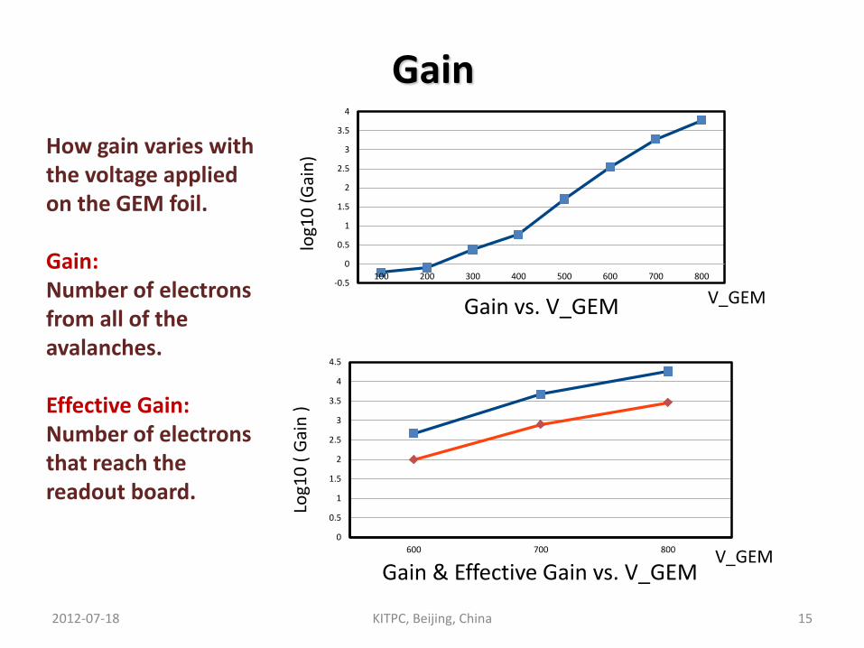
1. Particles which are accelerated by HI-13 pass through the kapton foil.
2. kapton etching,20um. 3. control the hole size by etching
time .
CIAE Nuclear Pore Foil
HI-13 tandem accelerator

Building Collaboration with a PCB Factory
Laminator Photoetching machine
Etching machine
The PCB factory is located in the south of Beijing. They would like to make the GEM foils for us if we provide the technology support.
8/16/2012 21 China Institute of Atomic Energy

Outline
1. Introduction
2. GEM Simulation
3. GEM foil
4. JLab GEM Test
5. Summary
2012-07-18 KITPC, Beijing, China 22

Chamber Structure
1. Three-Foil GEM Detector.
2. Work Gas Argon/CO2 = 70%/30%.
3. The whole Detector Setup consists of three chambers.
4. We used two scintilators to construct the coincidence signal.
2012-07-18 KITPC, Beijing, China 23
Top Cover
Drift
GEM 1
Read Out
Bottom Cover
GEM 2
GEM 3
Frame
Composition of a chamber
Gas in
Gas out
Detector System

Chamber Construction
Stretch
System
Re
ado
ut B
oard
Ch
amb
er in
bu
ildin
g
Ch
amb
er b
uilt
2012-07-18 KITPC, Beijing, China 24

Detector Prototype
2012-07-18 KITPC, Beijing, China 25
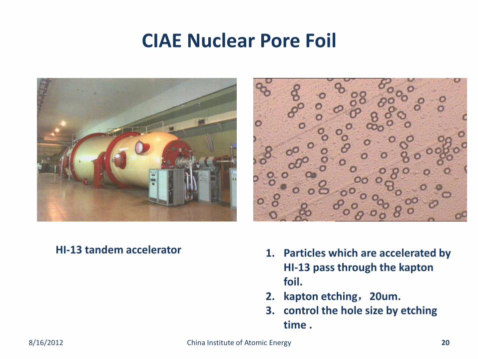
Readout Chip
Gassiplex Readout (not optimized for negative charge), 700 ns shaping time.
2012-07-18 KITPC, Beijing, China 26
Gassiplex Functional Module
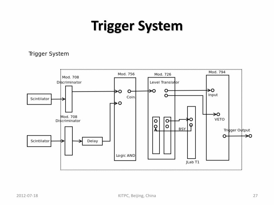
Trigger System
2012-07-18 KITPC, Beijing, China 27

Electronic System
1. Mod V551b controls the time sequence.
2. Mod V550 as the ADC Module.
2012-07-18 KITPC, Beijing, China 28

2012-07-18 KITPC, Beijing, China 29
Gassiplex Board
Pre-Amplifier Electronics System
Electronic System

ADC Distribution
adc x1 Entries 15962
Mean 785.5
RMS 565.6
0 200 400 600 800 1000120014001600180020000
100
200
300
400
500
adc x1 Entries 15962
Mean 785.5
RMS 565.6
X1 ADC
adc y1
Entries 7620
Mean 900.9
RMS 583.1
0 200 400 600 800 1000 1200 1400 1600 1800 20000
20
40
60
80
100
120
adc y1
Entries 7620
Mean 900.9
RMS 583.1
Y1 ADC
adc x2 Entries 6189
Mean 669.4
RMS 542.7
0 200 400 600 800 1000120014001600180020000
50
100
150
200
250
300
350
adc x2 Entries 6189
Mean 669.4
RMS 542.7
X2 ADC
adc y2
Entries 5454
Mean 710.8
RMS 537.4
0 200 400 600 800 1000 1200 1400 1600 1800 20000
20
40
60
80
100
120
140
160
180
adc y2
Entries 5454
Mean 710.8
RMS 537.4
Y2 ADC
adc x3 Entries 2945
Mean 386.3
RMS 414.4
0 200 400 600 800 1000 1200 1400 1600 1800 20000
50
100
150
200
250
300
350
adc x3 Entries 2945
Mean 386.3
RMS 414.4
X3 ADC
adc y3
Entries 2616Mean 546.9
RMS 421.7
0 200 400 600 800 1000 1200 1400 1600 1800 20000
20
40
60
80
100
120
adc y3
Entries 2616Mean 546.9
RMS 421.7
Y3 ADC
2012-07-18 KITPC, Beijing, China 30

ADC Distribution from Simulation
1. We can produce two peaks of the three.
2. The third peak is difficult to get due to the unstable gain.
2012-07-18 KITPC, Beijing, China 31
Simulation Setup
Simulation Results
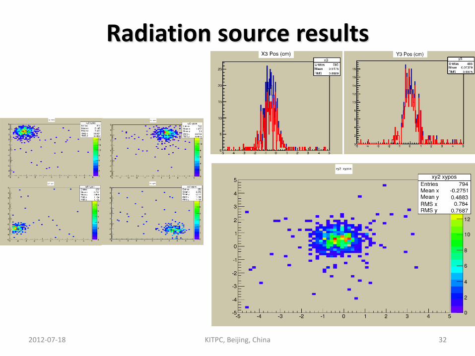
Radiation source results
2012-07-18 KITPC, Beijing, China 32
Outline
1. Introduction
2. GEM Simulation
3. GEM foil
4. JLab GEM Test
5. Summary
2012-07-18 KITPC, Beijing, China 33

Summary
1. We got some preliminary simulation results.
2. Further study of GEM foil
3. We will compare results from simulation and experiments in details.
2012-07-18 KITPC, Beijing, China 34
Gain Spatial Resolution Counting Rate Transparency

Thank you!
2012-07-18 KITPC, Beijing, China 35