Embed Size (px)
Citation preview

[01.2
017]
Mod.0818 2017-01 Rev.0
GE310-GNSS Hardware Design Guide
1VV0301564 Rev. 6 – 2019-04-02

GE310-GNSS Hardware Design Guide
1VV0301564 Rev. 5 Page 2 of 90 2019-01-23
SPECIFICATIONS ARE SUBJECT TO CHANGE WITHOUT NOTICE
NOTICE
While reasonable efforts have been made to assure the accuracy of this document, Telit assumes no liability resulting from any inaccuracies or omissions in this document, or from use of the information obtained herein. The information in this document has been carefully checked and is believed to be reliable. However, no responsibility is assumed for inaccuracies or omissions. Telit reserves the right to make changes to any products described herein and reserves the right to revise this document and to make changes from time to time in content hereof with no obligation to notify any person of revisions or changes. Telit does not assume any liability arising out of the application or use of any product, software, or circuit described herein; neither does it convey license under its patent rights or the rights of others.
It is possible that this publication may contain references to, or information about Telit products (machines and programs), programming, or services that are not announced in your country. Such references or information must not be construed to mean that Telit intends to announce such Telit products, programming, or services in your country.
COPYRIGHTS
This instruction manual and the Telit products described in this instruction manual may be, include or describe copyrighted Telit material, such as computer programs stored in semiconductor memories or other media. Laws in the Italy and other countries preserve for Telit and its licensors certain exclusive rights for copyrighted material, including the exclusive right to copy, reproduce in any form, distribute and make derivative works of the copyrighted material. Accordingly, any copyrighted material of Telit and its licensors contained herein or in the Telit products described in this instruction manual may not be copied, reproduced, distributed, merged or modified in any manner without the express written permission of Telit. Furthermore, the purchase of Telit products shall not be deemed to grant either directly or by implication, estoppel, or otherwise, any license under the copyrights, patents or patent applications of Telit, as arises by operation of law in the sale of a product.
COMPUTER SOFTWARE COPYRIGHTS
The Telit and 3rd Party supplied Software (SW) products described in this instruction manual may include copyrighted Telit and other 3rd Party supplied computer programs stored in semiconductor memories or other media. Laws in the Italy and other countries preserve for Telit and other 3rd Party supplied SW certain exclusive rights for copyrighted computer programs, including the exclusive right to copy or reproduce in any form the copyrighted computer program. Accordingly, any copyrighted Telit or other 3rd Party supplied SW computer programs contained in the Telit products described in this instruction manual may not be copied (reverse engineered) or reproduced in any manner without the express written permission of Telit or the 3rd Party SW supplier. Furthermore, the purchase of Telit products shall not be deemed to grant either directly or by implication, estoppel, or otherwise, any license under the copyrights, patents or patent applications of Telit or other 3rd Party supplied SW, except for the normal non-exclusive, royalty free license to use that arises by operation of law in the sale of a product.

GE310-GNSS Hardware Design Guide
1VV0301564 Rev. 5 Page 3 of 90 2019-01-23
USAGE AND DISCLOSURE RESTRICTIONS
I. License Agreements
The software described in this document is the property of Telit and its licensors. It is furnished by express license agreement only and may be used only in accordance with the terms of such an agreement.
II. Copyrighted Materials
Software and documentation are copyrighted materials. Making unauthorized copies is prohibited by law. No part of the software or documentation may be reproduced, transmitted, transcribed, stored in a retrieval system, or translated into any language or computer language, in any form or by any means, without prior written permission of Telit
III. High Risk Materials
Components, units, or third-party products used in the product described herein are NOT fault-tolerant and are NOT designed, manufactured, or intended for use as on-line control equipment in the following hazardous environments requiring fail-safe controls: the operation of Nuclear Facilities, Aircraft Navigation or Aircraft Communication Systems, Air Traffic Control, Life Support, or Weapons Systems (High Risk Activities”). Telit and its supplier(s) specifically disclaim any expressed or implied warranty of fitness for such High Risk Activities.
IV. Trademarks
TELIT and the Stylized T Logo are registered in Trademark Office. All other product or service names are the property of their respective owners.
V. Third Party Rights
The software may include Third Party Right software. In this case you agree to comply with all terms and conditions imposed on you in respect of such separate software. In addition to Third Party Terms, the disclaimer of warranty and limitation of liability provisions in this License shall apply to the Third Party Right software.
TELIT HEREBY DISCLAIMS ANY AND ALL WARRANTIES EXPRESS OR IMPLIED FROM ANY THIRD PARTIES REGARDING ANY SEPARATE FILES, ANY THIRD PARTY MATERIALS INCLUDED IN THE SOFTWARE, ANY THIRD PARTY MATERIALS FROM WHICH THE SOFTWARE IS DERIVED (COLLECTIVELY “OTHER CODE”), AND THE USE OF ANY OR ALL THE OTHER CODE IN CONNECTION WITH THE SOFTWARE, INCLUDING (WITHOUT LIMITATION) ANY WARRANTIES OF SATISFACTORY QUALITY OR FITNESS FOR A PARTICULAR PURPOSE.
NO THIRD PARTY LICENSORS OF OTHER CODE SHALL HAVE ANY LIABILITY FOR ANY DIRECT, INDIRECT, INCIDENTAL, SPECIAL, EXEMPLARY, OR CONSEQUENTIAL DAMAGES (INCLUDING WITHOUT LIMITATION LOST PROFITS), HOWEVER CAUSED AND WHETHER MADE UNDER CONTRACT, TORT OR OTHER LEGAL THEORY, ARISING IN ANY WAY OUT OF THE USE OR DISTRIBUTION OF THE OTHER CODE OR THE EXERCISE OF ANY RIGHTS GRANTED UNDER EITHER OR BOTH THIS LICENSE AND THE LEGAL TERMS APPLICABLE TO ANY SEPARATE FILES, EVEN IF ADVISED OF THE POSSIBILITY OF SUCH DAMAGES.

GE310-GNSS Hardware Design Guide
1VV0301564 Rev. 5 Page 4 of 90 2019-01-23
APPLICABILITY TABLE
PRODUCTS
GE310-GNSS

GE310-GNSS Hardware Design Guide
1VV0301564 Rev. 5 Page 5 of 90 2019-01-23
Contents
NOTICE 2
COPYRIGHTS ................................................................................................ 2
COMPUTER SOFTWARE COPYRIGHTS ...................................................... 2
USAGE AND DISCLOSURE RESTRICTIONS ............................................... 3
I. License Agreements ..................................................................... 3
II. Copyrighted Materials ................................................................... 3
III. High Risk Materials ....................................................................... 3
IV. Trademarks .................................................................................. 3
V. Third Party Rights ......................................................................... 3
APPLICABILITY TABLE ................................................................................ 4
CONTENTS .................................................................................................... 5
1. INTRODUCTION .......................................................................... 9
Scope ........................................................................................... 9
Audience....................................................................................... 9
Contact Information, Support ........................................................ 9
Text Conventions ........................................................................ 10
Related Documents .................................................................... 11
2. GENERAL PRODUCT DESCRIPTION ...................................... 12
Overview..................................................................................... 12
Product Variants and Frequency Bands ...................................... 12
Target market ............................................................................. 13
Main features .............................................................................. 13
TX Output Power ........................................................................ 14
Mechanical specifications ........................................................... 15
2.6.1. Dimensions ................................................................................. 15
3. PINS ALLOCATION ................................................................... 16
Pin-out ........................................................................................ 16
LGA Pads Layout ........................................................................ 24
4. POWER SUPPLY ....................................................................... 25
Power Supply Requirements ....................................................... 25
Power Consumption ................................................................... 26

GE310-GNSS Hardware Design Guide
1VV0301564 Rev. 5 Page 6 of 90 2019-01-23
General Design Rules ................................................................. 27
4.3.1. Electrical Design Guidelines ....................................................... 27
4.3.1.1. +5V Source Power Supply Design Guidelines ............................ 27
4.3.2. +12V Source Power Supply Design Guidelines .......................... 28
4.3.2.1. Battery Source Power Supply Design Guidelines ........................ 29
4.3.3. Thermal Design Guidelines ......................................................... 30
4.3.4. Power Supply PCB layout Guidelines ......................................... 31
RTC Bypass out .......................................................................... 32
VAUX Power Output ................................................................... 33
5. DIGITAL SECTION .................................................................... 34
Logic Levels ................................................................................ 34
Power On.................................................................................... 35
Power Off.................................................................................... 39
Unconditional Restart.................................................................. 41
5.4.1. PIN DESCRIPTION .................................................................... 41
5.4.2. Operating levels .......................................................................... 42
Communication ports .................................................................. 44
5.5.1. Serial Ports ................................................................................. 44
5.5.1.1. MODEM SERIAL PORT 0 (USIF0) ............................................. 44
5.5.1.2. MODEM SERIAL PORT 1 (USIF1) ............................................. 46
5.5.1.3. RS232 LEVEL TRANSLATION ................................................... 48
5.5.1.4. 5V UART level translation ........................................................... 51
General purpose I/O ................................................................... 52
5.6.1. Using a GPIO as INPUT ............................................................. 53
5.6.2. Using a GPIO as OUTPUT ......................................................... 54
5.6.3. Indication of network service availability ..................................... 54
External SIM Holder .................................................................... 55
6. GSM RF SECTION ..................................................................... 56
Antenna requirements................................................................. 56
6.1.1. Main Antenna ............................................................................. 56
6.1.2. PCB Design guidelines ............................................................... 57
6.1.2.1. Transmission line design ............................................................ 58
6.1.2.2. Transmission Line Measurements .............................................. 59
6.1.2.3. Antenna Installation Guidelines ................................................... 60
7. GNSS RECEIVER SECTION ...................................................... 61
Signals Description ..................................................................... 61

GE310-GNSS Hardware Design Guide
1VV0301564 Rev. 5 Page 7 of 90 2019-01-23
Power Consumption ................................................................... 61
GNSS Performances .................................................................. 62
GNSS Hosted configuration ........................................................ 63
GNSS Stand Alone configuration ................................................ 64
GNSS RF Front End Design ....................................................... 64
7.6.1. RF Signal Requirements ............................................................. 64
7.6.2. GPS Antenna Polarization .......................................................... 66
7.6.3. GPS Antenna Gain ..................................................................... 66
7.6.4. System Noise Floor .................................................................... 67
7.6.5. Active versus Passive Antenna ................................................... 67
7.6.6. GPS Antenna - PCB Line Guidelines .......................................... 67
7.6.7. RF Trace Losses ........................................................................ 68
7.6.8. Implications of the Pre-select SAW Filter .................................... 68
7.6.9. External LNA Gain and Noise Figure .......................................... 68
7.6.10. Powering the External LNA ......................................................... 69
7.6.11. External LNA Enable .................................................................. 70
7.6.12. Shielding ..................................................................................... 70
7.6.13. GPS Antenna – Installation ......................................................... 70
8. BLUETOOTH SECTION ............................................................. 71
Main Features ............................................................................. 71
Bluetooth Profiles ........................................................................ 71
8.2.1. Hands Free Gateway (HFG) ....................................................... 71
8.2.2. Phone Book Access Profile (PBAP) ............................................ 71
8.2.3. Phone Book Access Profile Client (PBAPC) ............................... 71
8.2.4. Serial Port Profile (SPP) ............................................................. 72
BLUETOOTH RF SECTION ....................................................... 72
8.3.1. Antenna requirements................................................................. 72
8.3.2. PCB Design guidelines ............................................................... 72
8.3.3. External Antenna ........................................................................ 73
8.3.4. Bluetooth Power Consumption .................................................... 74
9. AUDIO SECTION ....................................................................... 75
Analog Audio .............................................................................. 75
9.1.1. Signals Description ..................................................................... 75
10. MECHANICAL DESIGN ............................................................. 76
11. APPLICATION PCB DESIGN .................................................... 77
PCB pad design .......................................................................... 78

GE310-GNSS Hardware Design Guide
1VV0301564 Rev. 5 Page 8 of 90 2019-01-23
PCB pads ................................................................................... 78
Stencil ......................................................................................... 79
Solder paste ............................................................................... 79
Solder Reflow ............................................................................. 79
12. PACKAGING .............................................................................. 81
Tray ............................................................................................ 81
Moisture sensitivity ..................................................................... 83
13. CONFORMITY ASSESSMENT ISSUES .................................... 84
Approvals.................................................................................... 84
Declaration of Conformity ........................................................... 84
14. SAFETY RECOMMENDATIONS................................................ 85
READ CAREFULLY .................................................................... 85
15. REFERENCE TABLE OF RF BANDS CHARACTERISTICS ..... 86
16. ACRONYMS ............................................................................... 87
17. DOCUMENT HISTORY .............................................................. 89
GE310-GNSS Hardware Design Guide
1VV0301564 Rev. 5 Page 9 of 90 2019-01-23
1. INTRODUCTION
Scope
This document introduces the Telit GE310 modules and presents possible and recommended hardware solutions for developing a product based on this module. All the features and solutions detailed in this document are applicable to all GE310-GNSS variants, where GE310-GNSS refers to the variants listed in the applicability table.
Obviously, this document cannot embrace every hardware solution or every product that can be designed. Where the suggested hardware configurations need not be considered mandatory, the information given should be used as a guide and a starting point for properly developing your product with the Telit module.
Audience
This document is intended for Telit customers, especially system integrators, about to implement their applications using the Telit module.
Contact Information, Support
For general contact, technical support services, technical questions and report documentation errors contact Telit Technical Support at:
Alternatively, use:
http://www.telit.com/support
For detailed information about where you can buy the Telit modules or for recommendations on accessories and components visit:
http://www.telit.com
Our aim is to make this guide as helpful as possible. Keep us informed of your comments and suggestions for improvements.
Telit appreciates feedback from the users of our information.

GE310-GNSS Hardware Design Guide
1VV0301564 Rev. 5 Page 10 of 90 2019-01-23
Text Conventions
Danger – This information MUST be followed or catastrophic equipment failure or bodily injury may occur.
Caution or Warning – Alerts the user to important points about integrating the module, if these points are not followed, the module and end user equipment may fail or malfunction.
Tip or Information – Provides advice and suggestions that may be useful when integrating the module.
All dates are in ISO 8601 format, i.e. YYYY-MM-DD.

GE310-GNSS Hardware Design Guide
1VV0301564 Rev. 5 Page 11 of 90 2019-01-23
Related Documents
• Telit EVK2 User Guide, 1vv0300704

GE310-GNSS Hardware Design Guide
1VV0301564 Rev. 5 Page 12 of 90 2019-01-23
2. GENERAL PRODUCT DESCRIPTION
Overview
The GE310-GNSS is part of a new generation of modules in Telit’s 2G module portfolio.
With its compact LGA footprint, it is designed for those m2m applications requiring miniature foot print.
It is a quad-band 850/900/1800/1900 MHz GSM / GPRS communication product based on the market’ latest 2G core which allows integrators to plan on availability for even the longest lifecycle applications, highly recommended for new designs specified for 2G coverage worldwide.
It is including also a Bluetooth 4.0 transceiver and a GNSS Receiver.
It is highly recommended for new designs requiring 2G coverage in a small and robust LGA package, which implies easy integration and low impact on final application size and costs. Ease of production and small foot print makes it the ideal solution for applications in security alarms, automated meter reading, and pos terminals.
The product is fully voice capable, the analog and digital audio interfaces make it suitable for applications such as voice enabled alarm panels, mHealth patient monitors and specialty phones such as those for the elderly or sensory-impaired.
The GE310 operates with 2.8 V GPIOs, minimizing power consumption and making it even more ideally suited for battery powered and wearable device applications.
Product Variants and Frequency Bands
Product 2G Band (MHz)
3G Band (MHz)
4G Band (MHz)
Region
GE310-GNSS 850, 900, 1800, 1900
- - -
Refer to “RF Section” for details information about frequencies and bands.

GE310-GNSS Hardware Design Guide
1VV0301564 Rev. 5 Page 13 of 90 2019-01-23
Target market
GE310-GNSS can be used for telematics applications where tamper-resistance,
confidentiality, integrity, and authenticity of end-user information are required, for example:
• Emergency call
• Telematics services
• Road pricing
• Pay-as-you-drive insurance
• Stolen vehicles tracking
• Internet connectivity
Main features
Function Features
Modem • 2G (GSM/GPRS) Quad Band
• SMS support (text and PDU)
• Alarm management
• Real Time Clock
GNSS • GPS, Glonass, Galileo, Beidou, SBAS
Bluetooth • BT 4.0
Audio • Analog Audio
Interfaces • MAIN UART is typically used for:
o AT command access
o Diagnostic monitoring and debugging
• Secondary UART used to control GNSS
• GNSS UART
• USB port (Trace only)
• 6 GPIOs
• Antenna ports

GE310-GNSS Hardware Design Guide
1VV0301564 Rev. 5 Page 14 of 90 2019-01-23
TX Output Power
Band Power class
850/900 MHz Class 4 (2W)
1800/1900 MHz Class 1 (1W)

GE310-GNSS Hardware Design Guide
1VV0301564 Rev. 5 Page 15 of 90 2019-01-23
Mechanical specifications
2.6.1. Dimensions
The overall dimensions of GE310-GNSS family are:
Length: 15 mm
Width: 18 mm
Thickness: 2.6 mm

GE310-GNSS Hardware Design Guide
1VV0301564 Rev. 5 Page 16 of 90 2019-01-23
3. PINS ALLOCATION
Pin-out
Pin Signal I/O Function Type Comment
Asynchronous Serial Port (USIF0) – Prog. / Data + HW Flow Control
Y16 TXD0 I Serial data input (TXD) from DTE CMOS 2.8V
AA15 RXD0 O Serial data output (RXD) to DTE CMOS 2.8V
Y18 RTS0 I Input for Request to send signal (RTS) from DTE
CMOS 2.8V
AA17 CTS0 O Output for Clear to send signal (CTS) to DTE
CMOS 2.8V
Asynchronous Serial Port (USIF1)
Y12 TXD1 I Serial data input (TXD) from DTE CMOS 2.8V
AA11 RXD1 O Serial data output (RXD) to DTE CMOS 2.8V
Trace Port (USB)
U19 USB_D+ I/O USB differential Data (+)
V18 USB_D- I/O USB differential Data (-)
T18 USB_VBUS - Power sense for the internal USB transceiver
GNSS Serial Port
Y10 GNSS_NMEA_TX O GNSS UART UART (TX Data to DTE) CMOS 2.8V
AA9 GNSS_NMEA_RX I GNSS UART (RX Data from DTE) CMOS 2.8V
SIM card interface
L1 SIM_CLK O External SIM signal – Clock 1.8 / 3V
M2 SIM_RST O External SIM signal – Reset 1.8 / 3V
GE310-GNSS Hardware Design Guide
1VV0301564 Rev. 5 Page 17 of 90 2019-01-23
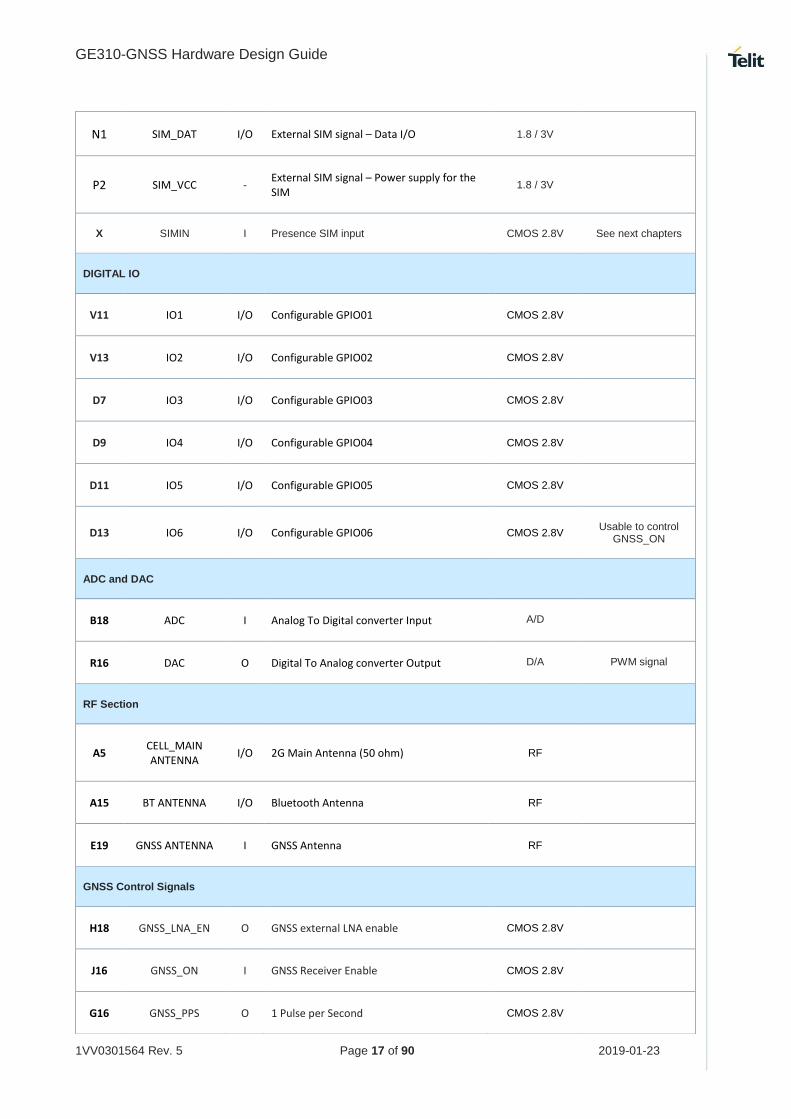
N1 SIM_DAT I/O External SIM signal – Data I/O 1.8 / 3V
P2 SIM_VCC - External SIM signal – Power supply for the SIM
1.8 / 3V
X SIMIN I Presence SIM input CMOS 2.8V See next chapters
DIGITAL IO
V11 IO1 I/O Configurable GPIO01 CMOS 2.8V
V13 IO2 I/O Configurable GPIO02 CMOS 2.8V
D7 IO3 I/O Configurable GPIO03 CMOS 2.8V
D9 IO4 I/O Configurable GPIO04 CMOS 2.8V
D11 IO5 I/O Configurable GPIO05 CMOS 2.8V
D13 IO6 I/O Configurable GPIO06 CMOS 2.8V Usable to control
GNSS_ON
ADC and DAC
B18 ADC I Analog To Digital converter Input A/D
R16 DAC O Digital To Analog converter Output D/A PWM signal
RF Section
A5 CELL_MAIN ANTENNA
I/O 2G Main Antenna (50 ohm) RF
A15 BT ANTENNA I/O Bluetooth Antenna RF
E19 GNSS ANTENNA I GNSS Antenna RF
GNSS Control Signals
H18 GNSS_LNA_EN O GNSS external LNA enable CMOS 2.8V
J16 GNSS_ON I GNSS Receiver Enable CMOS 2.8V
G16 GNSS_PPS O 1 Pulse per Second CMOS 2.8V

GE310-GNSS Hardware Design Guide
1VV0301564 Rev. 5 Page 18 of 90 2019-01-23
Miscellaneous Functions
B2 S_LED O Status LED CMOS 2.8V
N16 ON_OFF I Input Command for Power ON/OFF CMOS 2.8V
R19 RST I Reset CMOS 1.8V
B8 ALM O Alarm - RTC Indicator CMOS 2.8V
R1 VAUX O Supply Output for external accessories / Power ON Monitor
Power
Audio Section
C1 EAR+ AO Analog Audio (EAR+) Analog Class AB
D2 EAR- AO Analog Audio (EAR-) Analog Class AB
E1 MIC+ AI Analog Audio (MIC+) Analog
F2 MIC- AI Analog Audio (MIC-) Analog
Power Supply
W1 VBATT_PA - Main power supply (Radio PA) Power
AA3 VBATT - Main power supply (Baseband) Power
A3 GND - RF Ground Power
A7 GND - RF Ground Power
A9 GND - RF Ground Power
A13 GND - RF Ground Power
A17 GND - RF Ground Power
B4 GND - RF Ground Power
B6 GND - RF Ground Power

GE310-GNSS Hardware Design Guide
1VV0301564 Rev. 5 Page 19 of 90 2019-01-23
B10 GND - RF Ground Power
B12 GND - RF Ground Power
B14 GND - RF Ground Power
B16 GND - RF Ground Power
C19 GND - RF Ground Power
D18 GND - RF Ground Power
F8 GND - Thermal Ground Power
F12 GND - Thermal Ground Power
F18 GND - Thermal Ground Power
G19 GND - Thermal Ground Power
H6 GND - Thermal Ground Power
H14 GND - Thermal Ground Power
J19 GND - Thermal Ground Power
K18 GND - Thermal Ground Power
M18 GND - Thermal Ground Power
N19 GND - Thermal Ground Power
P6 GND - Thermal Ground Power
P14 GND - Thermal Ground Power
T8 GND - Thermal Ground Power
T12 GND - Thermal Ground Power
U1 GND - Power Ground Power
GE310-GNSS Hardware Design Guide
1VV0301564 Rev. 5 Page 20 of 90 2019-01-23
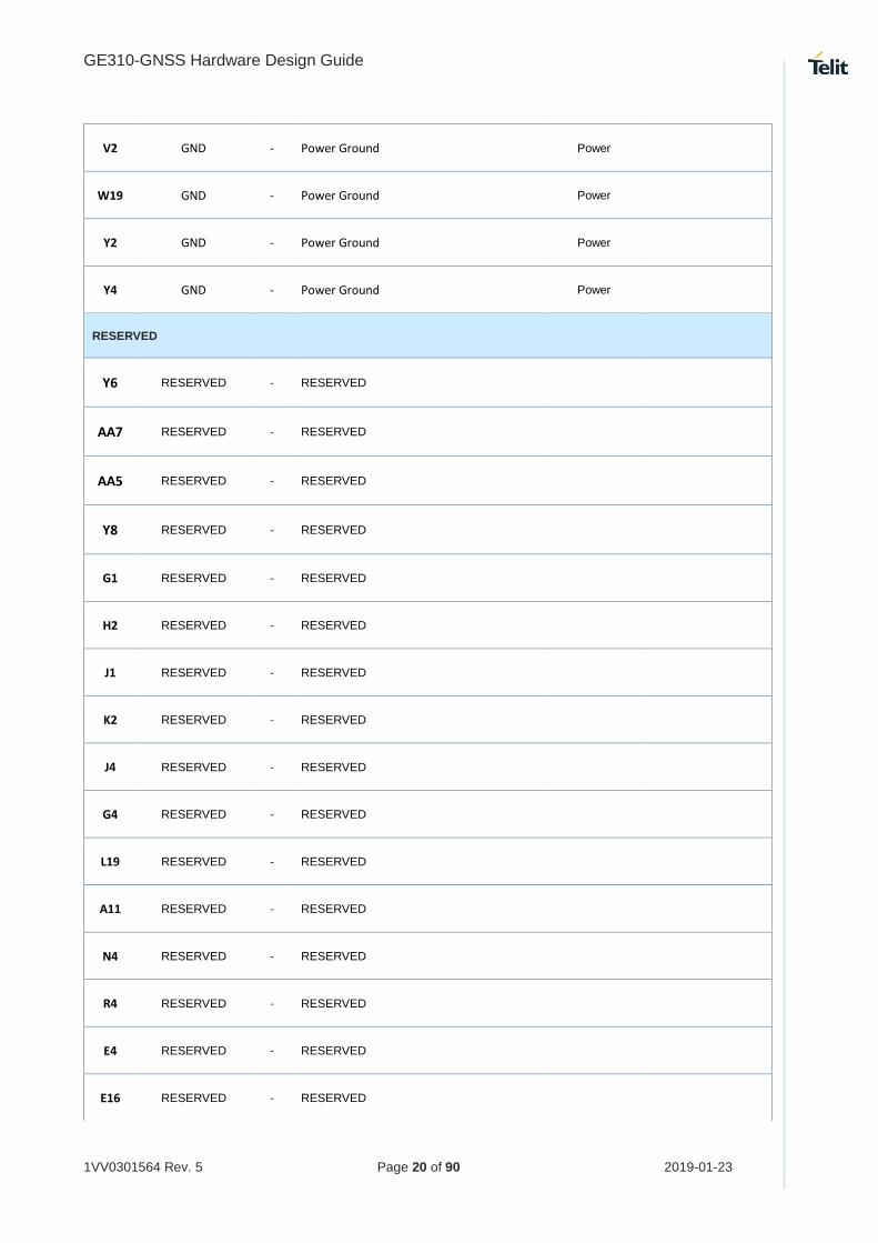
V2 GND - Power Ground Power
W19 GND - Power Ground Power
Y2 GND - Power Ground Power
Y4 GND - Power Ground Power
RESERVED
Y6 RESERVED - RESERVED
AA7 RESERVED - RESERVED
AA5 RESERVED - RESERVED
Y8 RESERVED - RESERVED
G1 RESERVED - RESERVED
H2 RESERVED - RESERVED
J1 RESERVED - RESERVED
K2 RESERVED - RESERVED
J4 RESERVED - RESERVED
G4 RESERVED - RESERVED
L19 RESERVED - RESERVED
A11 RESERVED - RESERVED
N4 RESERVED - RESERVED
R4 RESERVED - RESERVED
E4 RESERVED - RESERVED
E16 RESERVED - RESERVED

GE310-GNSS Hardware Design Guide
1VV0301564 Rev. 5 Page 21 of 90 2019-01-23
WARNING
Reserved pins must not be connected.
U4 RESERVED - RESERVED
U16 RESERVED - RESERVED
L4 RESERVED - RESERVED
V7 RESERVED - RESERVED
V9 RESERVED - RESERVED
L16 RESERVED - RESERVED
P18 RESERVED - RESERVED
AA13 RESERVED - RESERVED
Y14 RESERVED - RESERVED
T2 RESERVED - RESERVED

GE310-GNSS Hardware Design Guide
1VV0301564 Rev. 5 Page 22 of 90 2019-01-23
If not used, almost all pins should be left disconnected. The only exceptions are the
following pins:
Pad Signal Note
W1 VBATT_PA
AA3 VBATT
A3, A7, A9, A13, A17, B4, B6, B10, B12, B14, B16, C19,
D18, F8, F12, F18, G19, H6, H14, J19, K18, M18, N19, P6, P14, T8, T12, U1, V2, W19,
Y2, Y4
GND
A5 CELL_MAIN ANTENNA
A15 BT ANTENNA
E19 GNSS ANTENNA
Y16 C103/TXD0
AA15 C104/RXD0
Y18 C105/RTS0
AA17 C106/CTS0
T2 Reserved
N16 ON_OFF
R19 RST
R1 VAUX
L1 SIM_CLK
M2 SIM_RST
N1 SIM_DAT

GE310-GNSS Hardware Design Guide
1VV0301564 Rev. 5 Page 23 of 90 2019-01-23
RTS pin should be connected to the GND (on the module side) if flow control is not used.
The above pins are also necessary to debug the application when the module is
assembled on it so we recommend connecting them also to dedicated test point.
P2 SIM_VCC
D13 IO6
H18 GNSS_LNA_EN
J16 GNSS_ON
Y10 GNSS_NMEA_TX
AA9 GNSS_NMEA_RX
U19 USB_D+ On TP or a Connector
V18 USB_D- On TP or a Connector
T18 USB_VBUS On TP or a Connector

GE310-GNSS Hardware Design Guide
1VV0301564 Rev. 5 Page 24 of 90 2019-01-23
LGA Pads Layout
TOP VIEW

GE310-GNSS Hardware Design Guide
1VV0301564 Rev. 5 Page 25 of 90 2019-01-23
4. POWER SUPPLY
The power supply circuitry and board layout are a very important part in the full product
design and they strongly reflect on the product overall performances, hence read carefully
the requirements and the guidelines that will follow for a proper design.
Power Supply Requirements
The external power supply must be connected to VBATT & VBATT_PA signals and must
fulfil the following requirements:
Power Supply Value
Nominal Supply Voltage 3.8V
Operating Voltage Range 3.40 V÷ 4.20 V
NOTE:
The Operating Voltage Range MUST never be exceeded; care must
be taken when designing the application’s power supply section to
avoid having an excessive voltage drop.
If the voltage drop is exceeding the limits it could cause a Power Off
of the module.
Overshoot voltage (regarding MAX Extended Operating Voltage) and
drop in voltage (regarding MIN Extended Operating Voltage) MUST
never be exceeded;

GE310-GNSS Hardware Design Guide
1VV0301564 Rev. 5 Page 26 of 90 2019-01-23
Power Consumption
Mode Average (mA) Mode Description
Module OFF 0.160 Module switched OFF
AT+CFUN=1 13.2 Normal mode
AT+CFUN=4 12.2 Flight Mode
AT+CFUN=0 12.1 Turn off radio and SIM power
CSD TX/RX GSM850 / GSM900 (PL5)
223.2 GSM VOICE CALL
CSD TX/RX DCS1800 / PCS1900 (PL0)
132.3 GSM VOICE CALL
The GSM system is made in a way that the RF transmission is not continuous, but it is packed into bursts at a base frequency of approx. 217 Hz, and the relative current peaks can be as high as about 2A. Therefore the power supply has to be designed to withstand these current peaks without big voltage drops; this means that both the electrical design and the board layout must be designed for this current flow.
If the layout of the PCB is not well designed a strong noise floor is generated on the ground and the supply; this will reflect on all the audio paths producing an audible annoying noise at approx. 217 Hz; if the voltage drop during the peak current absorption is too much, then the device may even shutdown as a consequence of the supply voltage drop.
NOTE:
The electrical design for the Power supply should be made ensuring
it will be capable of a peak current output of at least 2 A.

GE310-GNSS Hardware Design Guide
1VV0301564 Rev. 5 Page 27 of 90 2019-01-23
General Design Rules
The principal guidelines for the Power Supply Design embrace three different design steps:
• the electrical design
• the thermal design
• the PCB layout.
4.3.1. Electrical Design Guidelines
The electrical design of the power supply depends strongly from the power source where this power is drained. We will distinguish them into three categories:
• +5V input (typically PC internal regulator output)
• +12V input (typically automotive)
• Battery
4.3.1.1. +5V Source Power Supply Design Guidelines
• The desired output for the power supply is 3.8V, hence there's not a big difference between the input source and the desired output and a linear regulator can be used. A switching power supply will not be suited because of the low drop out requirements.
• When using a linear regulator, a proper heat sink shall be provided in order to dissipate the power generated.
• A Bypass low ESR capacitor of adequate capacity must be provided in order to cut the current absorption peaks close to the module, a 100μF tantalum capacitor is usually suited.
• Make sure the low ESR capacitor on the power supply output (usually a tantalum one) is rated at least 10V.
• A protection diode should be inserted close to the power input, in order to save the module from power polarity inversion.
An example of linear regulator with 5V input is:

GE310-GNSS Hardware Design Guide
1VV0301564 Rev. 5 Page 28 of 90 2019-01-23
4.3.2. +12V Source Power Supply Design Guidelines
• The desired output for the power supply is 3.8V, hence due to the big difference between the input source and the desired output, a linear regulator is not suited and shall not be used. A switching power supply will be preferable because of its better efficiency especially with the 2A peak current load represented by the module.
• When using a switching regulator, a 500kHz or more switching frequency regulator is preferable because of its smaller inductor size and its faster transient response. This allows the regulator to respond quickly to the current peaks absorption.
• In any case the frequency and Switching design selection is related to the application to be developed due to the fact the switching frequency could also generate EMC interferences.
• For car PB battery the input voltage can rise up to 15,8V and this should be kept in mind when choosing components: all components in the power supply must withstand this voltage.
• A Bypass low ESR capacitor of adequate capacity must be provided in order to cut the current absorption peaks, a 100μF tantalum capacitor is usually suited.
• Make sure the low ESR capacitor on the power supply output (usually a tantalum one) is rated at least 10V.
• For Car applications a spike protection diode should be inserted close to the power input, in order to clean the supply from spikes.
• A protection diode should be inserted close to the power input, in order to save the module from power polarity inversion. This can be the same diode as for spike protection.
An example of switching regulator with 12V input is in the below schematic:

GE310-GNSS Hardware Design Guide
1VV0301564 Rev. 5 Page 29 of 90 2019-01-23
4.3.2.1. Battery Source Power Supply Design Guidelines
The desired nominal output for the power supply is 3.8V and the maximum voltage allowed is 4.2V, hence a single 3.7V Li-Ion cell battery type is suited for supplying the power to the Telit GE310-GNSS module.
• A Bypass low ESR capacitor of adequate capacity must be provided in order to cut the current absorption peaks, a 100μF tantalum capacitor is usually suited.
• Make sure the low ESR capacitor (usually a tantalum one) is rated at least 10V.
• A protection diode should be inserted close to the power input, in order to save the GE310-GNSS from power polarity inversion. Otherwise the battery connector should be done in a way to avoid polarity inversions when connecting the battery.
• The battery capacity must be at least 500mAh in order to withstand the current peaks of 2A; the suggested capacity is from 500mAh to 1000mAh.
WARNING:
The three cells Ni/Cd or Ni/MH 3,6 V Nom. Battery types or 4V PB
types MUST NOT BE USED DIRECTLY since their maximum voltage
can rise over the absolute maximum voltage for the GE310-GNSS
and damage it.
NOTE:
DON’T USE any Ni-Cd, Ni-MH, and Pb battery types directly
connected with GE310-GNSS. Their use can lead to overvoltage on
the GE310-GNSS and damage it. USE ONLY Li-Ion battery types.

GE310-GNSS Hardware Design Guide
1VV0301564 Rev. 5 Page 30 of 90 2019-01-23
4.3.3. Thermal Design Guidelines
The thermal design for the power supply heat sink should be done considering the values described in the “Power Consumption” chapter.
Considering the very low current during idle, especially if Power Saving function is enabled, it is possible to consider from the thermal point of view that the device absorbs current significantly only during calls.
For the heat generated by the module, you can consider it to be during transmission 1W max during CSD/VOICE calls and 2W max during class10 GPRS upload.
This generated heat will be mostly conducted to the ground plane under the module; you must ensure that your application can dissipate it.
NOTE:
The average consumption during transmissions depends on the
power level at which the device is requested to transmit by the
network. The average current consumption hence varies significantly.

GE310-GNSS Hardware Design Guide
1VV0301564 Rev. 5 Page 31 of 90 2019-01-23
4.3.4. Power Supply PCB layout Guidelines
As seen on the electrical design guidelines the power supply shall have a low ESR capacitor on the output to cut the current peaks and a protection diode on the input to protect the supply from spikes and polarity inversion. The placement of these components is crucial for the correct working of the circuitry. A misplaced component can be useless or can even decrease the power supply performance.
• The Bypass low ESR capacitor must be placed close to the Telit GE310-GNSS power input pads or in the case the power supply is a switching type it can be placed close to the inductor to cut the ripple provided the PCB trace from the capacitor to the GE310-GNSS is wide enough to ensure a dropless connection even during the 2A current peaks.
• The protection diode must be placed close to the input connector where the power source is drained.
• The PCB traces from the input connector to the power regulator IC must be wide enough to ensure no voltage drops occur when the 2A current peaks are absorbed. Note that this is not made in order to save power loss but especially to avoid the voltage drops on the power line at the current peaks frequency of approx. 217 Hz that will reflect on all the components connected to that supply, introducing the noise floor at the burst base frequency. For this reason while a voltage drop of 300-400 mV may be acceptable from the power loss point of view, the same voltage drop may not be acceptable from the noise point of view. If your application doesn't have audio interface but only uses the data feature of the Telit GE310-GNSS, then this noise is not so disturbing and power supply layout design can be more forgiving.
• The PCB traces to the GE310-GNSS and the Bypass capacitor must be wide enough to ensure no significant voltage drops occur when the 2A current peaks are absorbed. This is for the same reason as previous point. Try to keep this trace as short as possible.
• The PCB traces connecting the Switching output to the inductor and the switching diode must be kept as short as possible by placing the inductor and the diode very close to the power switching IC (only for switching power supply). This is done in order to reduce the radiated field (noise) at the switching frequency (100-500 kHz usually)
• The use of a good common ground plane is suggested.
• The placement of the power supply on the board should be done in such a way to guarantee that the high current return paths in the ground plane are not overlapped to any noise sensitive circuitry as the microphone amplifier/buffer or earphone amplifier.
• The power supply input cables should be kept separate from noise sensitive lines such as microphone/earphone cables.
• The insertion of EMI filter on VBATT pins is suggested in those designs where antenna is placed close to battery or supply lines.

GE310-GNSS Hardware Design Guide
1VV0301564 Rev. 5 Page 32 of 90 2019-01-23
• A ferrite bead like Murata BLM18EG101TN1 or Taiyo Yuden P/N FBMH1608HM101 can be used for this purpose. The below figure shows the recommended circuit:
RTC Bypass out
The GE310-GNSS module is provided by an internal RTC section but its reference supply is VBATT.
So, in order to maintain active the RTC programming, VBATT should not be removed

GE310-GNSS Hardware Design Guide
1VV0301564 Rev. 5 Page 33 of 90 2019-01-23
VAUX Power Output
A regulated power supply output is provided in order to supply small devices from the
module. The signal is in common with the PWRMON (module powered ON indication)
function. This output is always active when the module is powered ON. The operating
range characteristics of the supply are:
Item Min Typical Max
Output voltage 2.7V 2.80V 2.9V
Output current - - 10mA
Output bypass capacitor 1uF
NOTE:
The Output Current MUST never be exceeded; care must be taken
when designing the application section to avoid having an excessive
current consumption.
If the Current is exceeding the limits it could cause a Power Off of the
module.
NOTE:
VAUX max output current is shared with the other GPIOs for a
maximum load of 10mA.
Warning:
The current consumption from VAUX_PWRMON increases the
modem temperature.

GE310-GNSS Hardware Design Guide
1VV0301564 Rev. 5 Page 34 of 90 2019-01-23
5. DIGITAL SECTION
Logic Levels
ABSOLUTE MAXIMUM RATINGS:
Parameter Min Max
Input level on any digital pin (CMOS 2.8) with respect to ground
-0.3V 3.08
OPERATING RANGE – INTERFACE LEVELS (2.8V CMOS):
Parameter Min Max
Input high level 2.55V 2.9V
Input low level 0V 0.35V
Output high level 2.38V 2.8V
Output low level 0V 0.42V
CURRENT CHARACTERISTICS:
Parameter AVG
Input Current 10uA

GE310-GNSS Hardware Design Guide
1VV0301564 Rev. 5 Page 35 of 90 2019-01-23
Power On
To turn on the GE310 the pad ON_OFF* must be tied low for at least 1 seconds and then released.
The maximum current that can be drained from the ON_OFF* pad is 0,1 mA.
A simple circuit to do it is:
NOTE:
Don't use any pull up resistor on the ON_OFF* line, it is internally pulled up. Using pull up resistor may bring to latch up problems on the GE310 power regulator and improper power on/off of the module. The line ON_OFF* must be connected only in open collector or open drain configuration.
TIP:
To check if the device has powered on, the hardware line VAUX/PWRMON should be monitored.
NOTE:
It is mandatory to avoid sending data to the serial ports during the first 200ms of the module start-up.

GE310-GNSS Hardware Design Guide
1VV0301564 Rev. 5 Page 36 of 90 2019-01-23
A flow chart showing the proper turn on procedure is displayed below:
“Modem ON Proc”
START
Y
Y
GOTO
“HW SHUTDOWN unconditional”
GOTO
“Start AT CMD.”
N PWMON = ON ?
PWMON = ON ?
N
Delay 1s
ON_OFF* = LOW
Delay = 1 Sec
ON_OFF* = HIGH
“Modem ON Proc”
END
VBATT > 3.22V ?
Y
N

GE310-GNSS Hardware Design Guide
1VV0301564 Rev. 5 Page 37 of 90 2019-01-23
A flow chart showing the AT commands managing procedure is displayed below:
NOTE:
In order to avoid a back powering effect it is recommended to avoid having any HIGH logic level signal applied to the digital pins of the GE310 when the module is powered off or during an ON/OFF transition
AT answer in
1 sec ?
N
Y
“Start AT CMD.”
START
DELAY 300msec
Enter AT<CR>
“Start AT CMD.”
END
GOTO
“HW SHUTDOWN unconditional”
GOTO
“Modem ON Proc.”

GE310-GNSS Hardware Design Guide
1VV0301564 Rev. 5 Page 38 of 90 2019-01-23
For example:
1- Let's assume you need to drive the ON_OFF* pad with a totem pole output of a +3/5 V microcontroller (uP_OUT1):
2- Let's assume you need to drive the ON_OFF* pad directly with an ON/OFF button:

GE310-GNSS Hardware Design Guide
1VV0301564 Rev. 5 Page 39 of 90 2019-01-23
Power Off
The device could be turned off using the ON_OFF* pin
When the procedure is activated, the device issues a detach request to network informing
that the device will not be reachable any more.
To turn OFF the GE310 the pad ON_OFF* must be tied low for at least 3 seconds and
then released.
TIP:
To check if the device has been powered off, the hardware line PWRMON must be monitored. The device is powered off when PWRMON goes low
NOTE:
In order to avoid a back powering effect it is recommended to avoid having any HIGH logic level signal applied to the digital pins of the GE310 when the module is powered off or during an ON/OFF transition.

GE310-GNSS Hardware Design Guide
1VV0301564 Rev. 5 Page 40 of 90 2019-01-23
The following flow chart shows the proper turn off procedure:
Modem OFF Proc.
START
AT
Y
N PWMON = ON ?
OFF Mode
ON_OFF* = LOW
Delay >= 3 Sec
ON_OFF* = HIGH
“Modem OFF Proc”
END
PWRMON=ON?
Y
N
Key
AT#SHDN
GOTO
“HW Shutdown
Unconditional”
Looping for more
Y
N

GE310-GNSS Hardware Design Guide
1VV0301564 Rev. 5 Page 41 of 90 2019-01-23
Unconditional Restart
To unconditionally restart the GE310-GNSS, the pad RST must be tied low for at least
200 milliseconds and then released.
The hardware unconditional Restart must not be used during normal operation of the
device since it does not detach the device from the network. It shall be kept as an
emergency exit procedure to be done in the rare case that the device gets stuck waiting
for some network or SIM responses.
Do not use any pull up resistor on the RST line nor any totem pole digital output. Using
pull up resistor may bring to latch up problems on the GE310-GNSS power regulator and
improper functioning of the module.
The line RST must be connected only in open collector configuration; the transistor must
be connected as close as possible to the RST pin.
The unconditional hardware restart must always be implemented on the boards and the
software must use it as an emergency exit procedure.
5.4.1. PIN DESCRIPTION
Signal Function I/O Pad
RST Unconditional Reset of the Module I R19

GE310-GNSS Hardware Design Guide
1VV0301564 Rev. 5 Page 42 of 90 2019-01-23
5.4.2. Operating levels
The RST line is connected to VBATT with a Pull Up so the electrical levels on this pin are aligned to the main supply level.
WARNING:
The hardware unconditional Reset must not be used during normal
operation of the device since it does not detach the device from the
network. It shall be kept as an emergency exit procedure.
A typical circuit is the following:
NOTE:
In order to avoid a back powering effect it is recommended to avoid
having any HIGH logic level signal applied to the digital pins of the
GE310-GNSS when the module is powered off or during a reboot
transition.

GE310-GNSS Hardware Design Guide
1VV0301564 Rev. 5 Page 43 of 90 2019-01-23
NOTE:
Do not use any pull up resistor on the RST line nor any totem pole
digital output. Using pull up resistor may bring to latch up problems
on the GE310-GNSS power regulator and improper functioning of the
module.
To proper power on again the module please refer to the related
paragraph (“Power ON”)
The unconditional hardware reboot must always be implemented on
the boards and should be used only as an emergency exit procedure.

GE310-GNSS Hardware Design Guide
1VV0301564 Rev. 5 Page 44 of 90 2019-01-23
Communication ports
5.5.1. Serial Ports
The GE310-GNSS module is provided with by 2 Asynchronous serial ports:
• MODEM SERIAL PORT 0 (Main)
• MODEM SERIAL PORT 1
Several configurations can be designed for the serial port on the OEM hardware, but the most common are:
• RS232 PC com port
• microcontroller UART @ 2.8V (Universal Asynchronous Receive Transmit)
• microcontroller UART @ 5V or other voltages different from 2.8V
Depending from the type of serial port on the OEM hardware a level translator circuit may be needed to make the system work.
On the GE310-GNSS the ports are CMOS 2.8V.
5.5.1.1. MODEM SERIAL PORT 0 (USIF0)
The main serial port on the GE310-GNSS is a +2.8V UART with two flow control signals (CTS, RTS).
It differs from the PC-RS232 in the signal polarity (RS232 is reversed) and levels.
The following table is listing the available signals:
RS232 pin Signal PAD Name Usage
2 C104/RXD0 AA15 Transmit line *see Note
Output transmit line of GE310-GNSS UART
3 C103/TXD0 Y16 Receive line *see Note
Input receive of the GE310-GNSS UART
5 GND A3, A7, A9, A13, A17, B4, B6, B10, B12, B14, B16, C19, D18, F8, F12, F18, G19, H6, H14, J19, K18, M18, N19, P6, P14, T8, T12, U1, V2, W19, Y2, Y4
Ground Ground
7 C106/CTS0 AA17 Clear to Send Output from the GE310-GNSS that controls the Hardware flow control
8 C105/RTS0 Y18 Request to Send Input to the GE310-GNSS that controls the Hardware flow control

GE310-GNSS Hardware Design Guide
1VV0301564 Rev. 5 Page 45 of 90 2019-01-23
NOTE:
According to V.24, some signal names are referred to the application
side, therefore on the GE310-GNSS side these signal are on the
opposite direction:
TXD on the application side will be connected to the receive line
(here named C103/TXD0)
RXD on the application side will be connected to the transmit line
(here named C104/RXD0)
For a minimum implementation, only the TXD, RXD lines can be
connected, the other lines can be left open provided a software flow
control is implemented.
In order to avoid a back powering effect it is recommended to avoid
having any HIGH logic level signal applied to the digital pins of the
GE310-GNSS when the module is powered off or during a reboot
transition.

GE310-GNSS Hardware Design Guide
1VV0301564 Rev. 5 Page 46 of 90 2019-01-23
5.5.1.2. MODEM SERIAL PORT 1 (USIF1)
The secondary serial port on the GE310-GNSS is a +2.8V UART
It differs from the PC-RS232 in the signal polarity (RS232 is reversed) and levels.
The following table is listing the available signals:
RS232 pin Signal PAD Name Usage
2 RXD1 AA11 Transmit line *see Note
Output transmit line of GE310-GNSS UART
3 TXD1 Y12 Receive line *see Note
Input receive of the GE310-GNSS UART
5 GND A3, A7, A9, A13, A17, B4, B6, B10, B12, B14, B16, C19, D18, F8, F12, F18, G19, H6, H14, J19, K18, M18, N19, P6, P14, T8, T12, U1, V2, W19, Y2, Y4
Ground Ground
NOTE:
In order to avoid a back powering effect it is recommended to avoid
having any HIGH logic level signal applied to the digital pins of the
GE310-GNSS when the module is not supplied or during a reboot
transition.

GE310-GNSS Hardware Design Guide
1VV0301564 Rev. 5 Page 47 of 90 2019-01-23
NOTE:
According to V.24, some signal names are referred to the application
side, therefore on the GE310-GNSS side these signal are on the
opposite direction:
TXD on the application side will be connected to the receive line
(here named C103/TXD1)
RXD on the application side will be connected to the transmit line
(here named C104/RXD1)
In order to avoid a back powering effect it is recommended to avoid
having any HIGH logic level signal applied to the digital pins of the
GE310-GNSS when the module is powered off or during a reboot
transition.

GE310-GNSS Hardware Design Guide
1VV0301564 Rev. 5 Page 48 of 90 2019-01-23
5.5.1.3. RS232 LEVEL TRANSLATION
In order to interface the module with a PC com port or a RS232 (EIA/TIA-232) application
a level translator is required. This level translator must:
• invert the electrical signal in both directions;
• change the level from 0/2.8V to +15/-15V .
Actually, the RS232 UART 16450, 16550, 16650 & 16750 chipsets accept signals with
lower levels on the RS232 side (EIA/TIA-562), allowing a lower voltage-multiplying ratio
on the level translator. Note that the negative signal voltage must be less than 0V and
hence some sort of level translation is always required.
The simplest way to translate the levels and invert the signal is by using a single chip level
translator. There are a multitude of them, differing in the number of drivers and receivers
and in the levels (be sure to get a true RS232 level translator not a RS485 or other
standards).
By convention the driver is the level translator from the 0-2.8V UART to the RS232 level.
The receiver is the translator from the RS232 level to 0-2.8V UART.
In order to translate the whole set of control lines of the UART you will need:
• 2 drivers
• 2 receivers
NOTE:
The digital input lines working at 2.8V CMOS have an absolute
maximum input voltage of 3.0V; therefore the level translator IC shall
not be powered by the +3.8V supply of the module. Instead, it must
be powered from a +2.7V / +2.9V (dedicated) power supply.
This is because in this way the level translator IC outputs on the
module side (i.e. module’s inputs) will work at +3.8V interface levels,
damaging the module inputs

GE310-GNSS Hardware Design Guide
1VV0301564 Rev. 5 Page 49 of 90 2019-01-23
An example of level translation circuitry of this kind is:
The example is done with a MAXIM MAX3237 Transceiver that could accept supply
voltages of 3V DC. Not exceeded with supply voltage higher then 3.1VDC because this is
the higher voltage limit of module’s inputs.
NOTE:
In this case Vin has to be set with a value compatible with the logic
levels of the module. (Max 3.1V DC)

GE310-GNSS Hardware Design Guide
1VV0301564 Rev. 5 Page 50 of 90 2019-01-23
Second solution could be done using a MAXIM transceiver (MAX218) In this case the
compliance with RS232 (+-5V) is possible.
Another level adapting method could be done using a standard RS232 Transceiver
(MAX3237EAI) adding some resistors to adapt the levels on the module’s Input lines.
NOTE:
In this case has to be taken in account the length of the lines on the
application to avoid problems in case of High-speed rates on RS232.
The RS232 serial port lines are usually connected to a DB9 connector with the following
layout:

GE310-GNSS Hardware Design Guide
1VV0301564 Rev. 5 Page 51 of 90 2019-01-23
5.5.1.4. 5V UART level translation
If the OEM application uses a microcontroller with a serial port (UART) that works at a
voltage different from 2.8 - 3V, then a circuitry has to be provided to adapt the different
levels of the two set of signals. As for the RS232 translation there are a multitude of single
chip translators. For example a possible translator circuit for a 5V TRANSMITTER /
RECEIVER can be:
NOTE:
In order to avoid a back powering effect it is recommended to avoid
having any HIGH logic level signal applied to the digital pins of the
module when the module is powered OFF or during an ON/OFF
transition.

GE310-GNSS Hardware Design Guide
1VV0301564 Rev. 5 Page 52 of 90 2019-01-23
General purpose I/O
The GE310-GNSS module is provided by a set of Configurable Digital Input / Output pins
(CMOS 2.8V)
Input pads can only be read; they report the digital value (high or low) present on the pad
at the read time. Output pads can only be written or queried and set the value of the pad
output. An alternate function pad is internally controlled by the GE310-GNSS firmware
and acts depending on the function implemented.
The following table shows the available GPIO on the GE310-GNSS:
PAD Signal I/O Default State Note
V11 GPIO_01 I/O INPUT
V13 GPIO_02 I/O INPUT
D7 GPIO_03 I/O INPUT
D9 GPIO_04 I/O INPUT
D11 GPIO_05 I/O INPUT
D13 GPIO_06 I/O INPUT Usable to control GNSS_ON line
NOTE:
The internal GPIO’s pull up/pull down could be set to the preferred
status for the application using the AT#GPIO command.
Please refer for the AT Commands User Guide for the detailed
command Syntax.
WARNING:
During power up the GPIOs may be subject to transient glitches.

GE310-GNSS Hardware Design Guide
1VV0301564 Rev. 5 Page 53 of 90 2019-01-23
5.6.1. Using a GPIO as INPUT
The GPIO pads, when used as inputs, can be connected to a digital output of another
device and report its status, provided this device has interface levels compatible with the
2.8V CMOS levels of the GPIO. If the digital output of the device to be connected with the
GPIO input pad has interface levels different from the 2.8V CMOS, then it can be buffered
with an open collector transistor with a 47K pull up to VAUX.
NOTE:
In order to avoid a back powering effect it is recommended to avoid
having any HIGH logic level signal applied to the digital pins of the
GE310-GNSS when the module is powered off or during a reboot
transition.
The VAUX pin can be used for input pull up reference or/and for ON
monitoring.

GE310-GNSS Hardware Design Guide
1VV0301564 Rev. 5 Page 54 of 90 2019-01-23
5.6.2. Using a GPIO as OUTPUT
The GPIO pads, when used as outputs, can drive 2.8V CMOS digital devices or
compatible hardware. When set as outputs, the pads have a push-pull output and
therefore the pull-up resistor may be omitted.
5.6.3. Indication of network service availability
The S_LED pin status shows information on the network service availability and Call
status. In the GE310-GNSS modules, the SLED needs an external transistor to drive an
external LED. Therefore, the status indicated in the following table is reversed with
respect to the pin status.
Device Status Led Status
Device off Permanently off
Not Registered Permanently on
Registered in idle Blinking 1sec on + 2 sec off
Registered in idle + power saving It depends on the event that triggers the wakeup (In sync with network paging)
Voice Call Active Permanently on
Dial-Up Blinking 1 sec on + 2 sec off

GE310-GNSS Hardware Design Guide
1VV0301564 Rev. 5 Page 55 of 90 2019-01-23
A schematic example could be:
External SIM Holder
Please refer to the related User Guide (SIM Holder Design Guides, 80000NT10001a).

GE310-GNSS Hardware Design Guide
1VV0301564 Rev. 5 Page 56 of 90 2019-01-23
6. GSM RF SECTION
Antenna requirements
6.1.1. Main Antenna
The antenna connection and board layout design are the most important aspect in the full
product design as they strongly affect the product overall performances, hence read
carefully and follow the requirements and the guidelines for a proper design.
The antenna and antenna transmission line on PCB for a Telit GE310-GNSS device shall
fulfil the following requirements:
Item Value
Frequency range
824-894 MHz GSM850 band
880-960 MHz GSM900 band
1710-1885MHz DCS1800 band
1850-1990MHz PCS1900 band
Gain 1.4dBi @ GSM900 and 3dBi @ DCS1800
1.4dBi @ GSM850 and 3dBi @ PCS1900
Impedance 50 Ohm
Input power > 2 W
VSWR absolute max ≤ 10:1 (limit to avoid permanent damage)
VSWR recommended ≤ 2:1 (limit to fulfil all regulatory requirements)

GE310-GNSS Hardware Design Guide
1VV0301564 Rev. 5 Page 57 of 90 2019-01-23
6.1.2. PCB Design guidelines
When using the GE310-GNSS, since there’s no antenna connector on the module, the
antenna must be connected to the GE310-GNSS antenna pad by means of a
transmission line implemented on the PCB.
In the case the antenna is not directly connected at the antenna pad of the GE310-GNSS,
then a PCB line is needed in order to connect with it or with its connector.
This transmission line shall fulfil the following requirements:
Item Value
Characteristic Impedance 50 ohm
Max Attenuation 0,3 dB
Coupling Coupling with other signals shall be avoided
Ground Plane Cold End (Ground Plane) of antenna shall be equipotential to the GE310-GNSS ground pins
The transmission line should be designed according to the following guidelines:
• Ensure that the antenna line impedance is 50 ohm;
• Keep the antenna line on the PCB as short as possible, since the antenna line loss
shall be less than 0,3 dB;
• Antenna line must have uniform characteristics, constant cross section; avoid
meanders and abrupt curves;
• Keep, if possible, one layer of the PCB used only for the Ground plane;
• Surround (on the sides, over and under) the antenna line on PCB with Ground, avoid
having other signal tracks facing directly the antenna line track;
• The ground around the antenna line on PCB has to be strictly connected to the
Ground Plane by placing vias every 2mm at least;
• Place EM noisy devices as far as possible from GE310-GNSS antenna line;
• Keep the antenna line far away from the GE310-GNSS power supply lines;
• If you have EM noisy devices around the PCB hosting the GE310-GNSS, such as
fast switching Ics, take care of the shielding of the antenna line by burying it inside
the layers of PCB and surround it with Ground planes, or shield it with a metal frame
cover.

GE310-GNSS Hardware Design Guide
1VV0301564 Rev. 5 Page 58 of 90 2019-01-23
• If you don’t have EM noisy devices around the PCB of GE310-GNSS, by using a
micro strip on the superficial copper layer for the antenna line, the line attenuation
will be lower than a buried one;
6.1.2.1. Transmission line design
During the design of the GE310-GNSS interface board, the placement of components has
been chosen properly, in order to keep the line length as short as possible, thus leading to
lowest power losses possible. A Grounded Coplanar Waveguide (G-CPW) line has been
chosen, since this kind of transmission line ensures good impedance control and can be
implemented in an outer PCB layer as needed in this case. A SMA female connector has
been used to feed the line.
The interface board is realized on a FR4, 4-layers PCB. Substrate material is
characterized by relative permittivity εr = 4.6 ± 0.4 @ 1 GHz, TanD= 0.019 ÷ 0.026 @ 1
GHz.
A characteristic impedance of nearly 50 Ω is achieved using trace width = 1.1 mm,
clearance from coplanar ground plane = 0.3 mm each side. The line uses reference
ground plane on layer 3, while copper is removed from layer 2 underneath the line. Height
of trace above ground plane is 1.335 mm. Calculated characteristic impedance is 51.6 Ω,
estimated line loss is less than 0.1 dB. The line geometry is shown below:

GE310-GNSS Hardware Design Guide
1VV0301564 Rev. 5 Page 59 of 90 2019-01-23
6.1.2.2. Transmission Line Measurements
An HP8753E VNA (Full-2-port calibration) has been used in this measurement session.
A calibrated coaxial cable has been soldered at the pad corresponding to RF output; a
SMA connector has been soldered to the board in order to characterize the losses of the
transmission line including the connector itself. During Return Loss / impedance
measurements, the transmission line has been terminated to 50 Ω load.
Return Loss plot of line under test is shown below:
Line input impedance (in Smith Chart format, once the line has been terminated to 50 Ω
load) is shown in the following figure:

GE310-GNSS Hardware Design Guide
1VV0301564 Rev. 5 Page 60 of 90 2019-01-23
Insertion Loss of G-CPW line plus SMA connector is shown below:
6.1.2.3. Antenna Installation Guidelines
• Install the antenna in a place covered by the GSM signal.
• The Antenna must be installed to provide a separation distance of at least 20 cm
from all persons and must not be co-located or operating in conjunction with any
other antenna or transmitter;
• Antenna shall not be installed inside metal cases
• Antenna shall be installed also according Antenna manufacturer instructions.

GE310-GNSS Hardware Design Guide
1VV0301564 Rev. 5 Page 61 of 90 2019-01-23
7. GNSS RECEIVER SECTION
The GE310-GNSS module is provided by a GNSS receiver.
The GNSS receiver could be used as a stand alone device or as a hosted device for the
GSM/GPRS transceiver.
Signals Description
The Signals are available on the following Pads:
PAD Signal I/O Function
Y10 GNSS_NMEA_TX O GNSS UART UART (TX Data to DTE)
AA9 GNSS_NMEA_RX I GNSS UART (RX Data from DTE)
E19 GNSS ANTENNA I GNSS Antenna
H18 GNSS_LNA_EN O GNSS external LNA enable
J16 GNSS_ON I GNSS Receiver Enable
G16 GNSS_PPS O 1 Pulse per Second
Power Consumption
Mode Average (mA) Mode Description
GNSS OFF 0.011 GNSS section OFF
GNSS Acquisition 22.3 No GNSS signal available
GNSS Tracking 18.6 Tracking with signal CNR > 40dBHz

GE310-GNSS Hardware Design Guide
1VV0301564 Rev. 5 Page 62 of 90 2019-01-23
GNSS Performances
Sensitivity:
Mode Signal Level (dBm) Notes
Acquisition -140
Tracking -155
Navigation -155
TTFF:
Type Duration (sec) Notes
Hot Fix 1 Power @ -130dBm
Warm Fix 24 Power @ -130dBm
Cold Fix 24 Power @ -130dBm

GE310-GNSS Hardware Design Guide
1VV0301564 Rev. 5 Page 63 of 90 2019-01-23
GNSS Hosted configuration
This is the typical configuration for the GE310 where the GSM section is controlling the GNSS receiver.
The GPIO #6 (IO6) is used to control the GNSS Power ON pin (GNSS_ON), the
secondary serial port is used to manage the communication with the GNSS receiver and
to perform its SW upgrade. The TXD1 has to be connected with the GNSS_NMEA_TX,
the RXD1 has to be connected with the GNSS_NMEA_RX.
NOTE:
The SW upgrade of the GNSS section could be performed only in
Hosted configuration

GE310-GNSS Hardware Design Guide
1VV0301564 Rev. 5 Page 64 of 90 2019-01-23
GNSS Stand Alone configuration
In this configuration the GNSS is controlled by the external application so the NMEA sentences could be received from the GNSS_NMEA_RX and GNSS_NMEA_TX lines and the Power On of the GNSS is controlled by the external processor.
NOTE:
The SW upgrade of the GNSS section could be performed only in
Hosted configuration
GNSS RF Front End Design
The GE310-GNSS contains a pre-select SAW filter. This allows the receiver to work well with a passive GNSS antenna. For improved performance or if the antenna cannot be located near the GE310, an active antenna (that is, an antenna with a low noise amplifier built in) can be used. The following items will be discussed in turn to assist in designing the “RF front end”.
• RF signal requirements
• GNSS antenna polarization
• GNSS antenna gain
• System noise floor
• Active versus passive antenna
• RF trace losses
• Implications of the pre-select SAW filter
• External LNA gain and Noise Figure
• Powering the external LNA (active antenna)
• RF interference
• Shielding
7.6.1. RF Signal Requirements
The GE310-GNSS can achieve Cold Start acquisition with a signal level of -148 dBm at its input. This means the GE310 can find the necessary satellites, download the necessary ephemeris data and compute the location within a 5 minute period.
In the GNSS signal acquisition process, downloading and decoding the data is the most difficult task, which is why Cold Start acquisition requires a higher signal level than navigation or tracking signal levels. For the purposes of this discussion, autonomous operation is assumed, which makes the Cold Start acquisition level the important design constraint. If assistance data in the form of time or ephemeris aiding is available, then even lower signal levels can be used to compute a navigation solution.
The GNSS signal is defined by IS-GNSS-200E. This document states that the signal level received by a linearly polarized antenna having 3 dBi gain will be a minimum of -130 dBm when the antenna is in the worst orientation and the satellite is 5 degrees or more above the horizon.

GE310-GNSS Hardware Design Guide
1VV0301564 Rev. 5 Page 65 of 90 2019-01-23
In actual practice, the GNSS satellites are outputting slightly more power than specified by IS-GNSS-200E, and the signal level typically goes higher as the satellites have higher elevation angles.
The GE310-GNSS will display a reported C/No of 40 dB-Hz for a signal level of -130 dBm at the RF input.
Each GNSS satellite presents its own signal to the GE310, and best performance is obtained when the signal levels are between -130dbm and -125dBm. These received signal levels are determined by
• GNSS satellite transmit power
• GNSS satellite elevation and azimuth
• Free space path loss
• Extraneous path loss such as rain
• Partial or total path blockage such as foliage or building
• Multipath caused by signal reflection
• GNSS antenna
• Signal path after the GNSS antenna
The first three items in the list above are specified in IS-GNSS-200E, readily available multiple sources online. IS-GNSS-200E specifies a signal level minimum of -130 dBm will be presented to the receiver when using a linearly polarized antenna with 3 dBi gain.
The GNSS signal is relatively immune to rainfall attenuation and does not really need to be considered.
However, the GNSS signal is heavily influence by attenuation due to foliage, such as tree canopies, etc. as well as outright blockage caused by building, terrain or other items in the line of sight to the specific GNSS satellite. This variable attenuation is highly dependent upon GNSS satellite location. If enough satellites are blocked, say at a lower elevation, or all in a general direction, the geometry of the remaining satellites will result is a lower accuracy of position. The GE310 reports this geometry in the form of PDOP, HDOP and VDOP.
For example, in a vehicular application, the GNSS antenna may be placed embedded into the dashboard or rear package tray of an automobile. The metal roof of the vehicle will cause significant blockage, plus any thermal coating applied to the vehicle glass can attenuate the GNSS signal by as much as 15 dB. Again, both of these factors will affect the performance of the receiver.
Multipath is a phenomena where the signal from a particular satellite is reflected and is received by the GNSS antenna in addition to or in place of the original line of sight signal. The multipath signal has a path length that is longer than the original line of sight path and can either attenuate the original signal, or if received in place of the original signal can add additional error in determining a solution, because the distance to the particular GNSS satellite is actually longer than expected. It is this phenomena that makes GNSS navigation in urban canyons (narrow roads surround by high rise buildings) so challenging. In general, the reflecting of the GNSS signal causes the polarization to reverse. The implications of this are covered in the next section.

GE310-GNSS Hardware Design Guide
1VV0301564 Rev. 5 Page 66 of 90 2019-01-23
7.6.2. GPS Antenna Polarization
The GPS signal as broadcast is a right hand circularly polarized signal. The best antenna to receive the GPS signal is a right hand circularly (RHCP) polarized antenna.
Remember that IS-GPS-200E specifies the receive power level with a linearly polarized antenna. A linearly polarized antenna will have 3 dB loss as compared to an RHCP antenna assuming the same antenna gain (specified in dBi and dBic respectively).
An RHCP antenna is better at rejecting multipath than a linearly polarized antenna.
This is because the reflected signal changes polarization to LHCP, which would be rejected by the RHCP antenna by typically 20 dB or so. If the multipath signal is attenuating the line of sight signal, then the RHCP antenna would show a higher signal level than a linearly polarized antenna because the interfering signal is rejected.
However, in the case where the multipath signal is replacing the line of sight signal, such as in an urban canyon environment, then the number of satellites in view could drop below that needed to determine a 3D solution. This is a case where a bad signal may be better than no signal. The system designer needs to make tradeoffs in their application to determine which is the better choice.
7.6.3. GPS Antenna Gain
Antenna gain is defined as the extra signal power from the antenna as compared to a theoretical isotropic antenna (equally sensitive in all directions).
For example, a 25mm by 25m square patch antenna on a reference ground plane (usually 70mm by 70mm) will give an antenna gain at zenith of 5 dBic. A smaller 18mm by 18mm square patch on a reference ground plane (usually 50mm by 50mm) will give an antenna gain at zenith of 2 dBic.
While an antenna vendor will specify a nominal antenna gain (usually at zenith, or directly overhead) they should supply antenna pattern curves specifying gain as a function of elevation, and gain at a fixed elevation as a function of azimuth. Pay careful attention to the requirement to meet these specifications, such as ground plane required and any external matching components. Failure to follow these requirements could result in very poor antenna performance.
It is important to note that GPS antenna gain is not the same thing as external LNA gain. Most antenna vendors will specify these numbers separately, but some combine them into a single number. It is important to know both numbers when designing and evaluating the front end of a GPS receiver.
For example, antenna X has an antenna gain of 5 dBiC at azimuth and an LNA gain of 20 dB for a combined total of 25 dB. Antenna Y has an antenna gain of -5 dBiC at azimuth and an LNA gain of 30 dB for a combined total of 25 dB. However, in the system, antenna X will outperform antenna Y by about 10 dB (refer to next chapter for more details on system noise floor).
An antenna with higher gain will generally outperform an antenna with lower gain. Once the signals are above about -130 dBm for a particular satellite, no improvement in performance would be gained. However, for those satellites that are below about -125 dBm, a higher gain antenna would improve the gain and improve the performance of the GPS receiver. In the case of really weak signals, a good antenna could mean the difference between being able to use a particular satellite signal or not.

GE310-GNSS Hardware Design Guide
1VV0301564 Rev. 5 Page 67 of 90 2019-01-23
7.6.4. System Noise Floor
As mentioned earlier, the GE310 will display a reported C/No of 40 dB-Hz for an input signal level of -130 dBm. The C/No number means the carrier (or signal) is 40 dB greater than the noise floor measured in a one Hz bandwidth. This is a standard method of measuring GNSS receiver performance. The simplified formula is:
-174dbm + SNF – GNSS Signal level = C/No
Thermal noise is -174 dBm/Hz at 290K. From this we can compute a system noise figure of 4 dB for the GE310. This noise figure consists of the loss of the pre-select SAW filter, the noise figure of the LNA as well as implementation losses within the digital signal processing unit.
If a good quality external LNA is used with the GE310, then the noise figure of that LNA (typically better than 1dB) could reduce the overall system noise figure of the GE310 from 4 dB to around 2 dB. Some of the factors in the system noise figure are implementation losses due to quantization and other factors often referred to a digital noise or DSP noise and don’t scale with improved front end noise figure but are additive. The digital noise is typically around 1.0 -1.5dB. See next chapters for more information about reducing system noise by adding an external LNA.
7.6.5. Active versus Passive Antenna
If the GNSS antenna is placed near the GE310-GNSS and the RF trace losses are not excessive (nominally 1 dB), then a passive antenna can be used. This would normally be the lowest cost option and most of the time the simplest to use. However, if the antenna needs to be located away from the GE310 then an active antenna may be required to obtain the best system performance. The active antenna has its own built in low noise amplifier to overcome RF trace or cable losses after the active antenna.
However, an active antenna has a low noise amplifier (LNA) with associated gain and noise figure. In addition, many active antennas have a pre-select filter, a post-select filter or both.
7.6.6. GPS Antenna - PCB Line Guidelines
• Ensure that the antenna line impedance is 50ohm.
• Keep the antenna line on the PCB as short as possible to reduce the loss.
• Antenna line must have uniform characteristics, constant cross section, avoid meanders and abrupt curves.
• Keep one layer of the PCB used only for the Ground plane, if possible.
• Surround (on the sides, over and under) the antenna line on PCB with Ground, avoid having other signal tracks facing directly the antenna line of track.
• The ground around the antenna line on PCB has to be strictly connected to the Ground Plane by placing vias once per 2mm at least.
• Place EM noisy devices as far as possible from module’s antenna line.
• Keep the antenna line far away from the GE310 power supply lines.
• Keep the antenna line far away from the GE310 GSM RF lines.
• If you have EM noisy devices around the PCB hosting the GE310, such as fast switching ICs, take care of the shielding of the antenna line by burying it inside the

GE310-GNSS Hardware Design Guide
1VV0301564 Rev. 5 Page 68 of 90 2019-01-23
layers of PCB and surround it with Ground planes, or shield it with a metal frame cover.
• If you do not have EM noisy devices around the PCB of GE310, use a strip-line on the superficial copper layer for the antenna line. The line attenuation will be lower than a buried one.
7.6.7. RF Trace Losses
RF Trace losses are difficult to estimate on a PCB without having the appropriate tables or RF simulation software to estimate what the losses would be. A good rule of thumb would be to keep the RF traces as short as possible, make sure they are 50 ohms impedance and don’t contain any sharp bends.
7.6.8. Implications of the Pre-select SAW Filter
The GE310-GNSS module contains a SAW filter. Any circuit connected to the input of the GE310 would see a complex impedance presented by the SAW filter, particularly out of band, rather than the relatively broad and flat return loss presented by the LNA. Filter devices pass the desired in band signal, resulting in low reflected energy (good return loss), and reject the out of band signal by reflecting it back to the input, resulting in high reflected energy (bad return loss).
If an external amplifier is to be used with the GE310, the overall design should be checked for RF stability to prevent the external amplifier from oscillating. Amplifiers that are unconditionally stable at the output will be fine to use with the GE310-GNSS.
If an external filter is to be connected directly to the GE310, care needs to be used in making sure the external filter or the internal SAW filter performance is not compromised. These components are typically specified to operate into 50 ohms impedance, which is generally true in band, but would not be true out of band. If there is extra gain associated with the external filter, then a 6 dB Pi or T resistive attenuator is suggested to improve the impedance match between the two components.
7.6.9. External LNA Gain and Noise Figure
The GE310-GNSS can be used with an external LNA such as what might be found in an active antenna. Because of the internal LNA, the overall gain (including signal losses past the external LNA) should not exceed 14 dB. Levels higher than that can affect the jamming detection capability of the module. If a higher gain LNA is used, either a resistive Pi or T attenuator can be inserted after the LNA to bring the gain down to 14 dB.
The external LNA should have a noise figure better than 1 dB. This will give an overall system noise figure of around 2 dB assuming the LNA gain is 14 dB, or if higher the low gain mode is selected within the GE310. The overall system noise figure can be calculated using the Friss formula for cascaded noise figure. The simplified formula is shown below.
F is the total system noise, F1 is the noise figure of the external LNA, F2 is the noise figure of the internal LNA and G1 is the gain of the external LNA. In the GPS receiver the Digital noise is an additive number and cannot be reduced by reducing the System Noise figure.

GE310-GNSS Hardware Design Guide
1VV0301564 Rev. 5 Page 69 of 90 2019-01-23
The external LNA, if having no pre-select filter, needs to be able to handle signals other than the GNSS signal. These signals are typically at much higher levels. The amplifier needs to stay in the linear region when presented with these other signals. Again, the system designer needs to determine all of the unintended signals and their possible levels that can be presented making sure the external LNA will not be driven into compression. If this were to happen, the GNSS signal itself would start to be attenuated and the GNSS performance would suffer.
7.6.10. Powering the External LNA
The external LNA needs a source of power. Many of the active antennas accept a 3 volt or 5 volt DC voltage that is impressed upon the RF signal line. This voltage is not supplied by the GE310, but can be easily supplied by the host design.
Two approaches can be used. The first is to use an inductor to tie directly to the RF trace. This inductor should be at self-resonance at L1 (1.57542 GHz) and should have good Q for low loss. The higher the inductor Q, the lower the loss will be. The side of the inductor connecting to the antenna supply voltage should be bypassed to ground with a good quality RF capacitor, again operating at self-resonance at the L1 frequency.
The second approach is to use a quarter wave stub in place of the inductor. The length of the stub is designed to be exactly a quarter wavelength, which has the effect of making an RF short at L1 at one end of the stub to appear as an RF open. The RF short is created by the good quality RF capacitor operating at self-resonance.
The choice between the two would be determined by:
• RF path loss introduced by either the inductor or quarter wave stub.
• Cost of the inductor.
• Space availability for the quarter wave stub. Simulations done by Telit show the following:
o Murata LQG15HS27NJ02 Inductor 0.65 dB of additional signal loss o Quarter wave stub on FR4 0.59 dB of additional signal loss o Coilcraft B09TJLC Inductor 0.37 dB of additional signal loss
This additional loss occurs after the LNA so it is generally not significant unless the circuit is being designed to work with either an active or a passive antenna.

GE310-GNSS Hardware Design Guide
1VV0301564 Rev. 5 Page 70 of 90 2019-01-23
7.6.11. External LNA Enable
The GE310 is requiring an external LNA depending on the application.
The module is provided by a digital line usable to enable the power supply of the external amplifier. The signal is set to High only when the GPS receiver is active.
The line is named GNSS_LNA_EN
An example of GPS Antenna Supply circuit is shown in the following image:
7.6.12. Shielding
Shielding the RF circuitry generally is ineffective because the interference is getting into the GPS antenna itself, the most sensitive portion of the RF path. The antenna cannot be shielded because then it can’t receive the GPS signals.
There are two solutions, one is to move the antenna away from the source of interference or the second is to shield the digital interference to prevent it from getting to the antenna.
7.6.13. GPS Antenna – Installation
• The Antenna must not be co-located or operating in conjunction with any other antenna or transmitter.
• Antenna must not be installed inside metal cases.
• Antenna must be installed also according to the Antenna manufacturer instructions

GE310-GNSS Hardware Design Guide
1VV0301564 Rev. 5 Page 71 of 90 2019-01-23
8. BLUETOOTH SECTION
The GE310-GNSS Module is including a Bluetooth transceiver that requires only a minimum set of components to interface the external antenna.
The high sensitivity and class 1 output power ensure the connection with a wide range of Bluetoooth devices.
The module is fully compliant with Bluetooth v.4.0, including BR/EDR and BT low energy and offers enhanced data rates up to 3Mbps.
Main Features
• Fully compliant with BT 4.0 specification
• Low out-of Band spurious emissions support simultaneous operation with GPS and GSM/GPRS radio system.
• Low-IF architecture with high degree of linearity and high order channel filter
• Fully integrated PA provides 7.5dBm output power
• -95dBm sensitivity with excellent interference rejection performance
• Hardware AGC dynamically adjusts receiver performance in changing environments
• Up to 4 simultaneous active ACL links
• Up to 1 simultaneous SCO or eSCO link with CVSD coding
• Scatter net support Up to 4 piconets simultaneously with background inquiry/page scan
• Support of sniff mode
• Ultra-low power consumption states
Bluetooth Profiles
8.2.1. Hands Free Gateway (HFG)
This profile pemits to use a BT Handsfree
In this mode, the user can hear audio from remote device (connected via Bluetooth) while GSM modem is being used at the the remote side for incoming and outgoing call.
8.2.2. Phone Book Access Profile (PBAP)
Phone Book Access Profile (PBAP) is a profile that allows exchange of Phone Book items between devices.
8.2.3. Phone Book Access Profile Client (PBAPC)
To Support Phonebook access profile client. This permits the user to view phonebook of remote devices connected via Bluetooth.
The User will be able to edit the phonebook entires of the remote device and it can also make a call using the remote device entry.

GE310-GNSS Hardware Design Guide
1VV0301564 Rev. 5 Page 72 of 90 2019-01-23
8.2.4. Serial Port Profile (SPP)
This profile permits to emulate an RS232 port.
It is is based on ETSI 07.10 and the RFCOMM protocol. SPP maximum payload capacity is 128 bytes.
BLUETOOTH RF SECTION
8.3.1. Antenna requirements
The antenna connection and board layout design are the most important aspect in the full
product design as they strongly affect the product overall performances.
The antenna and antenna transmission line on PCB for a Telit GE310-GNSS device shall
fulfil the following requirements:
Item Value
Frequency range 2400 to 2483.5 MHz
8.3.2. PCB Design guidelines
When using the GE310-GNSS, since there’s no connector on the module, the antenna
must be connected to the GE310-GNSS RF pad (A15) by a line implemented on the PCB.
In the case the antenna is not directly connected at the BT antenna pad of the GE310-
GNSS, then a PCB line is needed in order to connect with it or with its connector.
This transmission line shall fulfil the following requirements:
Item Value
Characteristic Impedance 50 ohm
Max Attenuation 0,3 dB
Coupling Coupling with other signals shall be avoided
Ground Plane Cold End (Ground Plane) of antenna shall be equipotential to the GE310-GNSS ground pins

GE310-GNSS Hardware Design Guide
1VV0301564 Rev. 5 Page 73 of 90 2019-01-23
The transmission line should be designed according to the following guidelines:
• Ensure that the antenna line impedance is 50 ohm;
• Keep the antenna line on the PCB as short as possible, since the antenna line loss
shall be less than 0,3 dB;
• Antenna line must have uniform characteristics, constant cross section; avoid
meanders and abrupt curves;
• Keep, if possible, one layer of the PCB used only for the Ground plane;
• Surround (on the sides, over and under) the antenna line on PCB with Ground, avoid
having other signal tracks facing directly the antenna line track;
• The ground around the antenna line on PCB has to be strictly connected to the
Ground Plane by placing vias every 2mm at least;
• Place EM noisy devices as far as possible from GE310-GNSS antenna line;
• Keep the antenna line far away from the GE310-GNSS power supply lines;
• If you have EM noisy devices around the PCB hosting the GE310-GNSS, such as
fast switching Ics, take care of the shielding of the antenna line by burying it inside
the layers of PCB and surround it with Ground planes, or shield it with a metal frame
cover.
• If you don’t have EM noisy devices around the PCB of GE310-GNSS, by using a
micro strip on the superficial copper layer for the antenna line, the line attenuation
will be lower than a buried one;
8.3.3. External Antenna
In case of an application including a patch antenna you should include in the application design a matching circuit.

GE310-GNSS Hardware Design Guide
1VV0301564 Rev. 5 Page 74 of 90 2019-01-23
8.3.4. Bluetooth Power Consumption
Item Configuration Value (mA)
BT without Connect BT Interval = 2.56s
2G Standby (PG9, BA1) 1.3
BT Connect and Idle BT Interval = 1.28s
2G Standby (PG9, BA1) 1.8
BT Voice Active GSM 900 PLC19
without PA 73

GE310-GNSS Hardware Design Guide
1VV0301564 Rev. 5 Page 75 of 90 2019-01-23
9. AUDIO SECTION
The GE310-GNSS module is proving one Analog Audio section
Analog Audio
9.1.1. Signals Description The GE310-GNSS is provided by one Analog Audio section. The Signals are available on the following Pads:
PAD Signal I/O Function
C1 EAR+ O Analog Audio (EAR+)
D2 EAR- O Analog Audio (EAR-)
E1 MIC+ I Analog Audio (MIC+)
F2 MIC- I Analog Audio (MIC-)

GE310-GNSS Hardware Design Guide
1VV0301564 Rev. 5 Page 76 of 90 2019-01-23
10. MECHANICAL DESIGN
NOTE: The dimensions are in mm

GE310-GNSS Hardware Design Guide
1VV0301564 Rev. 5 Page 77 of 90 2019-01-23
11. APPLICATION PCB DESIGN
The GE310-GNSS modules have been designed in order to be compliant with a standard
lead-free SMT process.
In order to easily rework the GE310-GNSS is suggested to consider on the application a
1.5 mm placement inhibit area around the module. It is also suggested, as common rule
for an SMT component, to avoid having a mechanical part of the application in direct
contact with the module.
NOTE:
In the customer application, the region under WIRING INHIBIT (see
figure above) must be clear from signal or ground paths.
Units: mm

GE310-GNSS Hardware Design Guide
1VV0301564 Rev. 5 Page 78 of 90 2019-01-23
PCB pad design
Non solder mask defined (NSMD) type is recommended for the solder pads on the PCB.
PCB pads
It is not recommended to place via or micro-via not covered by solder resist in an area of
0,3 mm around the pads unless it carries the same signal of the pad itself.
Holes in pad are allowed only for blind holes and not for through holes.
Recommendations for PCB pad surfaces:
Finish Layer Thickness (um) Properties
Electro-less Ni / Immersion Au 3 –7 / 0.05 – 0.15 good solder ability protection,
high shear force values
The PCB must be able to resist the higher temperatures which are occurring at the lead-
free process. This issue should be discussed with the PCB-supplier. Generally, the
wettability of tin-lead solder paste on the described surface plating is better compared to
lead-free solder paste.
It is not necessary to panel the application’s PCB, however in that case it is suggested to
use milled contours and predrilled board breakouts; scoring or v-cut solutions are not
recommended.
PCB
Copper Pad Solder Mask
SMD
(Solder Mask Defined)
NSMD
(Non Solder Mask Defined)

GE310-GNSS Hardware Design Guide
1VV0301564 Rev. 5 Page 79 of 90 2019-01-23
Stencil
Stencil’s apertures layout can be the same of the footprint (1:1), we suggest a thickness of
stencil foil ≥ 120 µm.
Solder paste
Item Lead Free
Solder Paste Sn/Ag/Cu
We recommend using only “no clean” solder paste in order to avoid the cleaning of the
modules after assembly.
Solder Reflow
Recommended solder reflow profile:
Warning:
The above solder reflow profile represents the typical SAC reflow limits and does not guarantee adequate adherence of the module to the customer application throughout the temperature range. Customer must optimize the reflow profile depending on the overall system taking into account such factors as thermal mass and warpage

GE310-GNSS Hardware Design Guide
1VV0301564 Rev. 5 Page 80 of 90 2019-01-23
Profile Feature Pb-Free Assembly
Average ramp-up rate (TL to TP) 3°C/second max
Preheat
– Temperature Min (Tsmin)
– Temperature Max (Tsmax)
– Time (min to max) (ts)
150°C
200°C
60-180 seconds
Tsmax to TL
– Ramp-up Rate
3°C/second max
Time maintained above:
– Temperature (TL)
– Time (tL)
217°C
60-150 seconds
Peak Temperature (Tp) 245 +0/-5°C
Time within 5°C of actual Peak
Temperature (tp)
10-30 seconds
Ramp-down Rate 6°C/second max.
Time 25°C to Peak Temperature 8 minutes max.
NOTE:
All temperatures refer to topside of the package, measured on the
package body surface
WARNING:
THE GE310-GNSS MODULE WITHSTANDS ONE REFLOW
PROCESS ONLY.

GE310-GNSS Hardware Design Guide
1VV0301564 Rev. 5 Page 81 of 90 2019-01-23
12. PACKAGING
Tray
The GE310-GNSS modules are packaged on trays.
These trays can be used in SMT processes for pick & place handling.

GE310-GNSS Hardware Design Guide
1VV0301564 Rev. 5 Page 82 of 90 2019-01-23
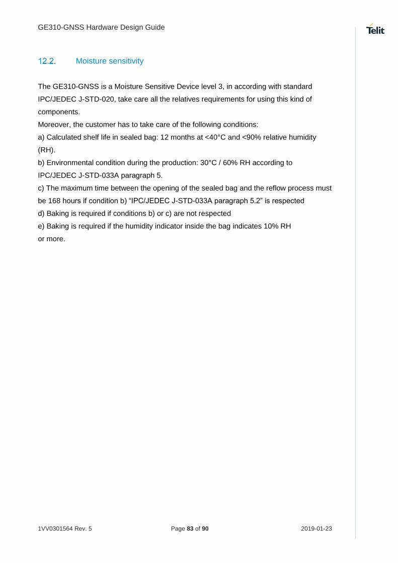
GE310-GNSS Hardware Design Guide
1VV0301564 Rev. 5 Page 83 of 90 2019-01-23
Moisture sensitivity
The GE310-GNSS is a Moisture Sensitive Device level 3, in according with standard
IPC/JEDEC J-STD-020, take care all the relatives requirements for using this kind of
components.
Moreover, the customer has to take care of the following conditions:
a) Calculated shelf life in sealed bag: 12 months at <40°C and <90% relative humidity
(RH).
b) Environmental condition during the production: 30°C / 60% RH according to
IPC/JEDEC J-STD-033A paragraph 5.
c) The maximum time between the opening of the sealed bag and the reflow process must
be 168 hours if condition b) “IPC/JEDEC J-STD-033A paragraph 5.2” is respected
d) Baking is required if conditions b) or c) are not respected
e) Baking is required if the humidity indicator inside the bag indicates 10% RH
or more.

GE310-GNSS Hardware Design Guide
1VV0301564 Rev. 5 Page 84 of 90 2019-01-23
13. CONFORMITY ASSESSMENT ISSUES
Approvals
GCF
RED
RoHS and REACH
Declaration of Conformity
The DoC is available here: https://www.telit.com/RED/

GE310-GNSS Hardware Design Guide
1VV0301564 Rev. 5 Page 85 of 90 2019-01-23
14. SAFETY RECOMMENDATIONS
READ CAREFULLY
Be sure the use of this product is allowed in the country and in the environment required.
The use of this product may be dangerous and has to be avoided in the following areas:
• Where it can interfere with other electronic devices in environments such as
hospitals, airports, aircrafts, etc.
• Where there is risk of explosion such as gasoline stations, oil refineries, etc. It is the
responsibility of the user to enforce the country regulation and the specific
environment regulation.
Do not disassemble the product; any mark of tampering will compromise the warranty
validity. We recommend following the instructions of the hardware user guides for correct
wiring of the product. The product has to be supplied with a stabilized voltage source and
the wiring has to be conformed to the security and fire prevention regulations. The product
has to be handled with care, avoiding any contact with the pins because electrostatic
discharges may damage the product itself. Same cautions have to be taken for the SIM,
checking carefully the instruction for its use. Do not insert or remove the SIM when the
product is in power saving mode.
The system integrator is responsible for the functioning of the final product; therefore, care
has to be taken to the external components of the module, as well as any project or
installation issue, because the risk of disturbing the LTE network or external devices or
having impact on the security. Should there be any doubt, please refer to the technical
documentation and the regulations in force. Every module has to be equipped with a proper
antenna with specific characteristics. The antenna has to be installed with care in order to
avoid any interference with other electronic devices and has to guarantee a minimum
distance from the body (20 cm). In case this requirement cannot be satisfied, the system
integrator has to assess the final product against the SAR regulation.
The European Community provides some Directives for the electronic equipment
introduced on the market. All of the relevant information is available on the European
Community website:
http://ec.europa.eu/enterprise/sectors/rtte/documents/
The text of the Directive 99/05 regarding telecommunication equipment is available,
while the applicable Directives (Low Voltage and EMC) are available at:
http://ec.europa.eu/enterprise/sectors/electrical/

GE310-GNSS Hardware Design Guide
1VV0301564 Rev. 5 Page 86 of 90 2019-01-23
15. REFERENCE TABLE OF RF BANDS CHARACTERISTICS
Mode Freq. Tx (MHz)
Freq. Rx (MHz)
Channels Tx-Rx Offset
PCS 1900 1850.2 ~ 1909.8 1930.2 ~ 1989.8 512 ~ 810 80 MHz
DCS 1800 1710 ~ 1785 1805 ~ 1880 512 ~ 885 95 MHz
GSM 850 824.2 ~ 848.8 869.2 ~ 893.8 128 ~ 251 45 MHz
EGSM 900 890 ~ 915 935 ~ 960 0 ~ 124 45 MHz
880 ~ 890 925 ~ 935 975 ~ 1023 45 MHz

GE310-GNSS Hardware Design Guide
1VV0301564 Rev. 5 Page 87 of 90 2019-01-23
16. ACRONYMS
TTSC Telit Technical Support Centre
USB Universal Serial Bus
HS High Speed
DTE Data Terminal Equipment
UMTS Universal Mobile Telecommunication System
WCDMA Wideband Code Division Multiple Access
HSDPA High Speed Downlink Packet Access
HSUPA High Speed Uplink Packet Access
UART Universal Asynchronous Receiver Transmitter
HSIC High Speed Inter Chip
SIM Subscriber Identification Module
SPI Serial Peripheral Interface
ADC Analog – Digital Converter
DAC Digital – Analog Converter
I/O Input Output
GPIO General Purpose Input Output
CMOS Complementary Metal – Oxide Semiconductor
MOSI Master Output – Slave Input

GE310-GNSS Hardware Design Guide
1VV0301564 Rev. 5 Page 88 of 90 2019-01-23
MISO Master Input – Slave Output
CLK Clock
MRDY Master Ready
SRDY Slave Ready
CS Chip Select
RTC Real Time Clock
PCB Printed Circuit Board
ESR Equivalent Series Resistance
VSWR Voltage Standing Wave Radio
VNA Vector Network Analyzer
TTFF Time to First Fix

GE310-GNSS Hardware Design Guide
1VV0301564 Rev. 5 Page 89 of 90 2019-01-23
17. DOCUMENT HISTORY
Revision Date Changes
0 2018-10-01 First emission – Preliminary
1 2018-10-30 Updated BT section
Added Power consumption values
2 2018-11-19 Updated Chapters 11 amd 12
Updatwd table in Chapter 3.1
3 2018-11-27 Updated Chapter 4.3.2.1, 4.3.4, 4.5, 5.3, 5.4.2, 5.5.1.2, 5.5.1.4
4 2019-01-16 Added Trace Port details
5 2019-01-23 Updated chapter 3.1, 3.2, 4.5 and 5.1
6 2019-04-02 Updated chapter 11, 11.5
Added GNSS performance data

[01.2
017]
Mod.0818 2017-01 Rev.0